KR101639574B1 - Image processing system supplying adaptive bank address and address mapping method thereof - Google Patents
Image processing system supplying adaptive bank address and address mapping method thereofDownload PDFInfo
- Publication number
- KR101639574B1 KR101639574B1KR1020090134573AKR20090134573AKR101639574B1KR 101639574 B1KR101639574 B1KR 101639574B1KR 1020090134573 AKR1020090134573 AKR 1020090134573AKR 20090134573 AKR20090134573 AKR 20090134573AKR 101639574 B1KR101639574 B1KR 101639574B1
- Authority
- KR
- South Korea
- Prior art keywords
- address
- bank
- tiles
- mapping
- image
- Prior art date
- Legal status (The legal status is an assumption and is not a legal conclusion. Google has not performed a legal analysis and makes no representation as to the accuracy of the status listed.)
- Active
Links
Images


Classifications
- G—PHYSICS
- G09—EDUCATION; CRYPTOGRAPHY; DISPLAY; ADVERTISING; SEALS
- G09G—ARRANGEMENTS OR CIRCUITS FOR CONTROL OF INDICATING DEVICES USING STATIC MEANS TO PRESENT VARIABLE INFORMATION
- G09G3/00—Control arrangements or circuits, of interest only in connection with visual indicators other than cathode-ray tubes
- G09G3/20—Control arrangements or circuits, of interest only in connection with visual indicators other than cathode-ray tubes for presentation of an assembly of a number of characters, e.g. a page, by composing the assembly by combination of individual elements arranged in a matrix no fixed position being assigned to or needed to be assigned to the individual characters or partial characters
- G—PHYSICS
- G06—COMPUTING OR CALCULATING; COUNTING
- G06F—ELECTRIC DIGITAL DATA PROCESSING
- G06F12/00—Accessing, addressing or allocating within memory systems or architectures
- G06F12/02—Addressing or allocation; Relocation
- G06F12/0223—User address space allocation, e.g. contiguous or non contiguous base addressing
- G06F12/0292—User address space allocation, e.g. contiguous or non contiguous base addressing using tables or multilevel address translation means
- G—PHYSICS
- G06—COMPUTING OR CALCULATING; COUNTING
- G06F—ELECTRIC DIGITAL DATA PROCESSING
- G06F12/00—Accessing, addressing or allocating within memory systems or architectures
- G06F12/02—Addressing or allocation; Relocation
- G06F12/06—Addressing a physical block of locations, e.g. base addressing, module addressing, memory dedication
- G06F12/0607—Interleaved addressing
- G—PHYSICS
- G09—EDUCATION; CRYPTOGRAPHY; DISPLAY; ADVERTISING; SEALS
- G09G—ARRANGEMENTS OR CIRCUITS FOR CONTROL OF INDICATING DEVICES USING STATIC MEANS TO PRESENT VARIABLE INFORMATION
- G09G5/00—Control arrangements or circuits for visual indicators common to cathode-ray tube indicators and other visual indicators
- G09G5/36—Control arrangements or circuits for visual indicators common to cathode-ray tube indicators and other visual indicators characterised by the display of a graphic pattern, e.g. using an all-points-addressable [APA] memory
- G09G5/39—Control of the bit-mapped memory
Landscapes
- Engineering & Computer Science (AREA)
- Theoretical Computer Science (AREA)
- Physics & Mathematics (AREA)
- General Physics & Mathematics (AREA)
- General Engineering & Computer Science (AREA)
- Computer Hardware Design (AREA)
- Memory System (AREA)
- Controls And Circuits For Display Device (AREA)
Abstract
Translated fromKoreanDescription
Translated fromKorean본 발명은 전자 장치에 관한 것으로, 좀 더 구체적으로는 이미지 포맷에 따라 적응적으로 뱅크 어드레스를 생성하는 디스플레이 시스템 및 그것의 어드레스 맵핑 방법에 관한 것이다.BACKGROUND OF THE
최근 들어서는, 노트북, 휴대폰, PDA, 디지털카메라 등과 같은 휴대형 정보기기의 사용이 급증하고 있다. 또한, 휴대형이 아니더라도 다양한 분야에서 다양한 목적으로 정보기기들이 사용되고 있다. 이들 정보기기들에는 정보의 표시 수단으로서 또는 사용자와의 인터페이싱을 위한 수단으로서 디스플레이 시스템이 포함된다. 정보기기들 각각의 디스플레이 시스템들은 용도나 목적에 따라 다양한 해상도와 품질의 이미지를 표시하게 될 것이다.In recent years, the use of portable information devices such as notebook computers, mobile phones, PDAs, and digital cameras has been rapidly increasing. In addition, although not portable, information devices are used for various purposes in various fields. These information devices include a display system as means for displaying information or as means for interfacing with a user. Information devices Each display system will display images of various resolutions and qualities depending on the purpose and purpose.
디스플레이 시스템은 디지털 이미지를 통하여 사용자(User)에게 정보를 표시하고 전달한다. 디지털 이미지는 문자 또는 숫자나, 그래프 및 그림 등의 형태로 제공될 수 있다. 많은 응용에서, 디지털 이미지들은 모니터(Monitor)나 프린 터(Printer)와 같은 디스플레이 장치에 표시됨으로써 사용자들에게 전달된다. 이미지들은 맵핑(Mapping) 메모리에 디지털 데이터의 형태로 저장되었다가, 일정한 조작을 거쳐 디스플레이 상에 나타나게 된다.The display system displays and transmits information to a user through a digital image. The digital image can be provided in the form of letters, numbers, graphs, pictures, and the like. In many applications, digital images are presented to users by being displayed on a display device such as a monitor or a printer. The images are stored in the form of digital data in a mapping memory, and then displayed on the display through a certain operation.
그러므로 디스플레이 시스템에서는 디스플레이의 데이터를 저장하는 맵핑 메모리가 필요하다. 그리고 디지털 형태로 저장된 데이터를 디스플레이 상에서 영상으로 표현하기 위해서는 맵핑(Mapping) 작업이 필요하다. 맵핑 작업은 맵핑 메모리 상의 특정 영역 데이터가 디스플레이 상의 특정 바이트(Byte)에 영상으로 처리되도록 한다. 그리고 맵핑 메모리로는 동기식 디램(SDRAM)과 같은 반도체 메모리 장치가 사용된다.Therefore, the display system requires a mapping memory for storing the data of the display. In order to display the data stored in the digital form on the display, a mapping operation is required. The mapping operation allows specific area data on the mapping memory to be processed into a specific byte (Byte) on the display. A semiconductor memory device such as synchronous DRAM (SDRAM) is used as the mapping memory.
이미지의 디스플레이 성능을 결정하는 요소들에는 마이크로프로세서의 속도, 메모리의 액세스 시간 등이 있다. 그리고 그 이외의 디스플레이 성능을 결정하는 요소들에는 디스플레이의 사이즈, 맵핑 메모리의 용량이나 어드레스 맵핑 방식 등이 있다.Factors that determine the display performance of an image include the speed of the microprocessor and the access time of the memory. Other factors that determine the display performance include the size of the display, the capacity of the mapping memory, and the address mapping method.
맵핑 메모리의 어드레스 맵핑 방식에는 라인 지향(Line Oriented) 방식과 타일 지향(Tile Oriented) 방식이 있다. 라인 지향 방식의 디스플레이 시스템은 디스플레이 상에 하나의 라인씩 나타나도록 순차적 순서에 따라 데이터를 발생하고 저장한다. 즉, 맵핑 메모리로의 데이터의 저장 및 맵핑 메모리로부터 디스플레이로의 데이터의 리드는 하나의 비트씩 및 하나의 라인씩 수행된다. 타일 지향 방식의 디스플레이 시스템은 디스플레이 상에 타일(Tile)이라고 불리우는 동일한 크기와 형태의 표시 단위로 맵핑 메모리에 데이터를 저장하고 읽어낸다. 타일들의 크기와 형 태는 시스템 설계자들 및 사용자들에 의하여 선택되는 요소들 중의 하나이다. 예를 들면, 이들 타일들은 정사각형 또는 직사각형이 될 수 있다.The address mapping method of the mapping memory includes a line-oriented method and a tile-oriented method. A line-oriented display system generates and stores data in a sequential order so that one line appears on the display. That is, the storage of data in the mapping memory and the reading of data from the mapping memory to the display are performed one bit at a time and one line at a time. The tile-oriented display system stores and reads data in the mapping memory in the same size and type of display unit called a tile on the display. The size and shape of tiles is one of the factors chosen by system designers and users. For example, these tiles can be square or rectangular.
타일 지향 방식의 디스플레이 시스템은 디스플레이 화면을 동시에 리프레쉬하므로, 동작 속도의 측면에서 이점을 가진다. 즉, 다수의 데이터 비트를 한 묶음으로 처리함으로써 리프레쉬 효율을 개선시킨다. 이와 같은 타일 중심의 디스플레이와 맵핑 작업을 수행하기 위해서는 많은 수를 데이터를 동시에 입출력할 수 있는 맵핑 메모리가 요구된다.The display system of the tile-oriented method refreshes the display screen at the same time, and thus has an advantage in terms of operation speed. That is, a plurality of data bits are processed in a bundle to improve the refresh efficiency. In order to perform the display and mapping operation of such a tile center, a mapping memory capable of simultaneously inputting / outputting a large number of data is required.
현재, 맵핑 메모리로 사용되는 동기식 디램(DRAM)에서는 독립적으로 액세스될 수 있는 복수의 뱅크들을 포함한다. 복수의 타일이 포함되는 특정 영역의 이미지 데이터를 맵핑 메모리에 저장할 때, 동일 뱅크의 서로 다른 행에 특정 영역의 이미지 데이터가 저장될 수 있다. 이 경우, 특정 영역의 이미지 데이터를 액세스하기 위해서는 선택된 뱅크에서 행 어드레스(Row address)의 전환이 필요하다. 따라서, 이미 열린 행에 대한 클로즈 사이클과 새로운 행을 열기 위한 오픈 사이클이 더 소요된다. 이러한 문제를 오픈-로-액세스(Open-Row-Access)라고 하며, 시스템의 성능 저하의 주된 요인으로 작용한다. 따라서, 오픈-로-액세스(Open-Row-Access) 문제를 해결할 수 있는 맵핑 방식이 필요하다. 또한, 다양한 포맷의 디스플레이 시스템들에 대해 적용될 수 있는 적응적이고 효율적인 맵핑 방식에 대한 요구가 절실한 실정이다.Presently, a synchronous DRAM (DRAM) used as a mapping memory includes a plurality of banks that can be independently accessed. When image data of a specific area including a plurality of tiles is stored in the mapping memory, image data of a specific area can be stored in different rows of the same bank. In this case, in order to access the image data of the specific area, it is necessary to switch the row address in the selected bank. Therefore, it takes more time for an open cycle to open a row and an open cycle to open a new row. This problem is called Open-Row-Access, which is a major factor in system performance degradation. Therefore, there is a need for a mapping scheme that can solve the open-row-access problem. There is also a need for an adaptive and efficient mapping scheme that can be applied to display systems of various formats.
본 발명의 목적은 어드레스 맵핑 방식을 적응적으로 선택하고 액세스 성능을 높일 수 있는 이미지 처리 시스템 및 그것의 어드레스 발생 방법을 제공하는 데 있다.An object of the present invention is to provide an image processing system and its address generation method capable of adaptively selecting an address mapping scheme and improving access performance.
상기 목적을 달성하기 위한 본 발명의 실시 예에 따른 디스플레이 시스템은, 이미지 데이터를 복수의 타일 단위로 표시하는 디스플레이, 상기 이미지 데이터를 상기 복수의 타일 단위로 저장하며, 복수의 타일들 각각을 복수의 뱅크들 중 어느 하나의 뱅크에 할당하는 맵핑 메모리, 그리고 상기 복수의 타일들 각각을 상기 복수의 뱅크들에 순차적으로 할당하기 위한 제 1 어드레스와, 상기 복수의 타일들 중 짝수 또는 홀수 행의 타일들에 할당되는 뱅크 어드레스를 인터리빙하기 위한 제 2 어드레스 중 어느 하나를 상기 맵핑 메모리에 제공하는 이미지 맵핑부를 포함한다.According to an aspect of the present invention, there is provided a display system for displaying image data in a plurality of tile units, storing the image data in units of a plurality of tiles, A first address for sequentially allocating each of the plurality of tiles to the plurality of banks and a first address for sequentially assigning tiles of even or odd rows among the plurality of tiles, And a second address for interleaving the bank address allocated to the address mapping unit.
상술한 목적을 달성하기 위한 본 발명의 실시 예에 따른 복수의 뱅크들을 포함하는 메모리에 이미지를 저장하기 위한 어드레스 맵핑 방법은, 상기 이미지를 복수의 타일들로 분할하고, 상기 복수의 타일들 각각을 상기 복수의 뱅크들에 순차적으로 할당하는 제 1 어드레스를 생성하는 단계, 상기 제 1 어드레스에 의해 상기 이미지상의 어느 하나의 타일과 상기 어느 하나의 타일에 인접하는 타일들이 동일한 뱅크에 할당되었는지를 검출하는 단계, 그리고 상기 이미지상의 어느 하나의 타일과 상기 어느 하나의 타일에 인접하는 타일들이 동일한 뱅크에 할당되는 것으로 검출되는 경우, 상기 제 1 어드레스의 뱅크 할당을 재설정한 제 2 어드레스를 생성하는 단계를 포함한다.According to an aspect of the present invention, there is provided an address mapping method for storing an image in a memory including a plurality of banks, the method including dividing the image into a plurality of tiles, The method comprising: generating a first address to be sequentially allocated to the plurality of banks; detecting, by the first address, whether one of the tiles on the image and tiles adjacent to the one tile are allocated to the same bank And generating a second address that resets the bank assignment of the first address when it is detected that any tile on the image and tiles adjacent to the tile are assigned to the same bank do.
본 발명의 실시 예에 따르면, 이미지 포맷에 따라 어드레스 맵핑 방식을 재설정할 수 있고, 액세스 속도를 높일 수 있는 이미지 처리 시스템을 구성할 수 있다.According to the embodiment of the present invention, the address mapping method can be reset according to the image format, and the image processing system capable of increasing the access speed can be configured.
앞의 일반적인 설명 및 다음의 상세한 설명 모두 예시적이라는 것이 이해되어야 하며, 청구된 발명의 부가적인 설명이 제공되는 것으로 여겨져야 한다. 참조 부호들이 본 발명의 바람직한 실시 예들에 상세히 표시되어 있으며, 그것의 예들이 참조 도면들에 표시되어 있다. 가능한 어떤 경우에도, 동일한 참조 번호들이 동일한 또는 유사한 부분을 참조하기 위해서 설명 및 도면들에 사용된다.It is to be understood that both the foregoing general description and the following detailed description are exemplary and should provide a further description of the claimed invention. Reference numerals are shown in detail in the preferred embodiments of the present invention, examples of which are shown in the drawings. Wherever possible, the same reference numbers are used in the description and drawings to refer to the same or like parts.
아래에서, 동기식 디램(SDRAM)이 본 발명의 특징 및 기능을 설명하기 위한 맵핑 메모리의 한 예로서 사용된다. 하지만, 이 기술 분야에 정통한 사람은 여기에 기재된 내용에 따라 본 발명의 다른 이점들 및 성능을 쉽게 이해할 수 있을 것이다. 예를 들면, 저장 매체로서 SRAM, PRAM, MRAM, ReRAM, FRAM, NOR 플래시 메모리 등이 사용될 수 있다. 또한, 본 발명은 다른 실시 예들을 통해 구현되거나 적용될 수 있을 것이다. 게다가, 상세한 설명은 본 발명의 범위, 기술적 사상 그리고 다른 목적으로부터 상당히 벗어나지 않고 관점 및 사용에 따라 수정되거나 변경될 수 있다.In the following, synchronous DRAM (SDRAM) is used as an example of a mapping memory for explaining the features and functions of the present invention. However, those skilled in the art will readily appreciate other advantages and capabilities of the present invention in accordance with the teachings herein. For example, SRAM, PRAM, MRAM, ReRAM, FRAM, NOR flash memory and the like can be used as the storage medium. Further, the present invention may be implemented or applied through other embodiments. Moreover, the detailed description can be modified or changed in accordance with the viewpoint and use without departing from the scope of the present invention, technical idea and other objects.
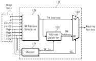
도 1은 본 발명의 실시 예에 따른 을 보여주는 블록도이다. 도 1을 참조하면, 디스플레이 시스템(1000)은 이미지 데이터와 어드레스를 제공하는 이미지 맵핑 부(100)와 맵핑 메모리(200), 그리고 디스플레이(300)를 포함한다.1 is a block diagram illustrating an embodiment of the present invention. Referring to FIG. 1, a
이미지 맵핑부(100)는 이미지 데이터를 생성하는 프로세서(110)와 어드레스 발생기(120)를 포함한다. 프로세서(110)는 입력되는 디지털 이미지를 디스플레이 상에서 복수의 타일들로 구분하고, 타일들 각각에 대응하는 이미지 데이터(Image data)를 생성한다. 만일, 사용자가 이미지상에서 특정 영역을 선택하면, 프로세서(110)는 전체 이미지의 크기와 타일 크기, 선택된 영역의 위치 및 크기에 관련된 이미지 데이터(Image data)를 어드레스 발생기(120)로 전달한다.The
어드레스 발생기(120)는 이미지 데이터(Image data)를 참조하여 맵핑 어드레스(SBFTM Address)를 생성한다. 어드레스 발생기(120)는 오픈-로-액세스(Open-Row-Access)와 같은 오버헤드 문제를 최소화하기 위하여 맵핑 어드레스(SBFTM Address)를 적응적 또는 선택적으로 생성한다. 어드레스 발생기(120)는 입력되는 이미지 데이터(Image Data)를 분석한다. 어드레스 발생기(120)는 분석 결과에 따라 맵핑 메모리(200)에 대한 복수의 맵핑 방식들 중 최적의 어드레스 맵핑 방식을 결정한다. 어드레스 발생기(120)는 결정된 최적의 어드레스 맵핑 방식에 따라 맵핑 어드레스(Mapping Address)를 생성하고, 맵핑 메모리(200)로 제공한다.The
맵핑 메모리(200)는 서로 독립적으로 액세스될 수 있는 복수의 뱅크를 포함한다. 뱅크에 있어서 하나의 행을 페이지(Page)라 한다. 각각의 페이지에는 앞서 설명된 하나의 타일에 대응하는 이미지 데이터가 저장될 수 있다. 하지만, 페이지와 타일의 관계는 여기에 국한되지는 않는다. 타일에 대응하는 데이터의 크기가 페이지보다 작을 수도 있다.The
디스플레이(300)에는 맵핑 메모리(200)에 저장되는 이미지 데이터가 영상으로 표시된다. 디스플레이(300)는 예를 들면, CRT 모니터, LCD 모니터와 같은 다양한 형태의 디스플레이 수단들을 포함할 수 있다.In the
도 2는 도 1의 어드레스 발생기(120)를 상세하게 보여주는 블록도이다. 도 2를 참조하면, 어드레스 발생기(120)는 타일 맵핑 어드레스 발생기(121), 어드레스 변환기(122), 어드레스 선택부(123), 검출기(124)를 포함한다.FIG. 2 is a block diagram showing the
타일 맵핑 어드레스 발생기(121)는 이미지 데이터(Image data)를 제공받아 타일 맵핑 어드레스(TM Address)로 변환한다. 타일 맵핑 어드레스 발생기(121)에 제공되는 이미지 데이터에는 선택된 특정 이미지 영역의 위치와 크기 정보(x, y, xsize, ysize) 그리고 전체 이미지의 크기 정보(ImgH, ImgV), 타일의 크기 정보(TileH, TileV)를 포함한다. 이미지 데이터를 참조하여, 타일 맵핑 어드레스 발생기(121)는 맵핑 메모리(200) 상에서 입력되는 이미지 데이터를 저장하기 위한 타일 어드레스를 생성한다.The tile
어드레스 변환기(122)는 타일 맵핑 어드레스 발생기(121)로부터 출력되는 타일 맵핑 어드레스(TM Address)를 뱅크 플립 어드레스(BF Address)로 변환한다. 어드레스 변환기(122)는 검출기(124)에 의해서 제공되는 뱅크 플립 인에이블(BF_En)신호에 따라 타일 맵핑 어드레스(TM Address)를 뱅크 플립 어드레스(BF Address)로 변환한다. 이러한 변환의 예는 후술하는 도 6에서 상세히 설명될 것이다.The
어드레스 선택부(123)는 검출기(124)로부터 제공되는 선택 신호(SEL)에 응답하여 타일 맵핑 어드레스(TM Address)와 뱅크 플립 어드레스(BF Address) 중 어느 하나를 선택한다. 타일 맵핑 어드레스(TM Address)와 뱅크 플립 어드레스(BF Address) 중 어드레스 선택부(123)에 의해 선택된 어드레스가 맵핑 메모리(200)의 어드레스로 제공될 것이다.The
검출기(124)는 입력되는 이미지 데이터(Image Data)를 참조하여, 어드레스 맵핑 방식을 선택한다. 검출기(124)는 이미지 데이터(Image Data)를 이용하여 해당하는 이미지의 포맷 또는 사이즈에 최적화되는 뱅크 어드레스의 맵핑 방식을 계산한다. 검출기(124)는 맵핑 메모리(200)에 포함되는 뱅크의 수, 페이지의 크기를 추가적으로 사용하여 뱅크 어드레스의 맵핑 방식을 선택하기 위한 계산을 수행할 수 있다. 검출기(124)는 다양한 사이즈 또는 포맷의 이미지에 대해서 적응적으로 적용될 수 있는 뱅크 어드레스의 맵핑 방식을 결정할 수 있다. 이러한 결정을 위하여, 검출기(124)는 이미지의 수평 크기에 수용 가능한 타일의 수(T value)를 계산한다. 검출기(124)는 계산 결과로 출력되는 타일 수(T value)를 참조하여 최적 성능을 나타내는 어드레스 맵핑 방식을 선택한다. 그리고 검출기(124)는 계산 결과를 참조하여 타일 맵핑(Tile Mapping: TM) 방식이 적절한지 또는 뱅크 플립 맵핑(Bank Flipping mapping:BF) 방식이 적절한지를 결정한다.The
이상의 도 2에서 기술된 어드레스 발생기(120)에 따르면, 어떤 포맷의 이미지에 대해서도 맵핑 메모리(200)의 구조에 최적화된 어드레스 맵핑이 가능하다. 그리고 어드레스 발생기(120)에 의하여 사용자가 이미지의 특정 영역을 선택하더라도, 동일 뱅크에서 서로 다른 행을 액세스해야하는 오픈-로-액세스와 같은 오버헤드를 차단할 수 있다.According to the
도 3은 도 1의 맵핑 메모리(200)의 메모리 영역을 간략히 보여주는 표이다. 도 3을 참조하면, 맵핑 메모리(200)의 메모리 영역은 복수의 뱅크(Bank)로 구분된다. 그리고 각각의 뱅크들은 m개(m은 자연수)의 행들과 n(n은 자연수)개의 열들로 이루어져 있다. 여기서, 하나의 뱅크에 포함되는 하나의 행을 페이지(Page)라 칭한다. 예를 들면, 빗금친 영역은 뱅크0(Bank0)의 행10(Row10)에 해당하는 페이지(Page)이다. 하나의 뱅크는 페이지 단위로 액세스될 수 있으며, 이러한 액세스를 페이지 모드 액세스라고도 한다.FIG. 3 is a table briefly showing a memory area of the
뱅크들 각각은 서로 독립적인 액세스를 지원한다. 즉, 뱅크0(Bank0)의 어느 하나의 행에 대한 읽기 동작중, 뱅크3(Bank3)의 다른 하나의 행에 대한 액세스가 가능하다. 따라서, 뱅크 어드레스가 전환되는 읽기 요청시에는 오버헤드가 발생하지 않는다.Each of the banks supports independent access to each other. In other words, during a read operation for any one row of the bank 0 (Bank 0), access to the other row of the bank 3 (Bank 3) is possible. Therefore, overhead does not occur at the time of the read request in which the bank address is switched.
그러나, 동일한 뱅크 내에서 어느 하나의 행에 대한 읽기 동작중, 다른 하나의 행에 대한 읽기 요청이 발생하면 상대적으로 큰 오버헤드가 발생한다. 왜냐하면, 현재 읽기 중인 행에 대한 클로즈 사이클과 읽기 요청된 다른 행에 대한 오픈 사이클이 추가되기 때문이다. 즉, 이 경우 오픈-로-액세스(Open-Row-Access)가 발생한다. 맵핑 메모리(200)에 이미지 데이터를 저장할 때, 이러한 문제를 최대한 회피할 수 있는 방식으로 뱅크 어드레스를 생성해야 한다. 즉, 동일 뱅크의 서로 다른 행에 할당되는 데이터를 다른 뱅크로 어드레스를 재배열하여 이러한 오버헤드를 감소시킬 필요가 있다.However, a relatively large overhead occurs when a read request for another row occurs during a read operation for any one row in the same bank. This is because a close cycle for the row currently being read and an open cycle for another row that is requested to be read are added. That is, in this case, open-row-access occurs. When storing image data in the
도 4a, 4b 4c, 그리고 4d는 도 2의 타일 맵핑 어드레스 발생기(121)에 의한 어드레스 발생 과정을 보여주는 도면들이다.4A, 4B, 4C, and 4D are diagrams showing an address generation process by the tile
도 4a에는 하나의 이미지(400)가 도시되어 있다. 이미지(400)를 구성하는 픽셀들 각각의 데이터는 맵핑 메모리(200)에 타일 단위로 저장될 것이다. 이를 위해서, 이미지(400)를 구성하는 픽셀 데이터는 복수의 타일 단위로 분할될 수 있다. 분할된 각각의 타일 단위의 픽셀 데이터는 타일 맵핑 어드레스 발생기(121)에 의해서 생성되는 맵핑 메모리(200) 상의 물리적 위치에 저장된다. 만일, 사용자가 이미지(400) 중에서 확대나 편집을 위해서 위치 (x, y) 및 사이즈 (xsize, ysize)를 가지는 영역을 선택하였다 가정하자. 선택 영역(410)의 픽셀 데이터는 하나의 타일에 포함될 수도 있지만, 복수의 타일들에 걸쳐서 맵핑될 수 있다. 본 발명의 실시 예에서는 선택 영역(410)에 대한 액세스 시에 오픈-로-액세스가 발생하지 않도록 타일 맵핑 또는 뱅크 플립 맵핑이 적용될 것이다.One
도 4b는 도 4a의 이미지(400)를 복수의 타일 단위로 분할한 예를 간략히 보여주는 도면이다. 타일 맵핑을 위해서, 이미지(400)는 수평으로 3분할, 수직으로 4분할되도록 구분된다. 그리고, 분할된 각각의 타일들에는 타일 번호들(①~⑫)이 할당된다. 이렇게 타일이 정의되면, 각각의 타일에 포함되는 픽셀 데이터들과 맵핑 메모리(200)의 페이지들이 맵핑된다. 타일들 각각의 화살표들은 맵핑 메모리(200)에 저장되기 위한 픽셀들의 어드레스 순서이다. 선택 영역(410)의 픽셀 데이터들은 4개의 타일들(④, ⑤, ⑦, ⑧)로 맵핑된다.FIG. 4B is a view showing an example of dividing the
도 4c는 분할된 각각의 타일들의 픽셀 데이터가 저장되는 맵핑 메모리(200)의 뱅크들간의 대응 관계를 보여주는 도면이다. 하나의 타일에 대응하는 픽셀 데이 터와 맵핑 메모리(200)의 페이지 용량이 동일하게 2KByte라 가정하자. 그러면, 타일(①)에 대응하는 픽셀 데이터들은 맵핑 메모리(200)의 뱅크0(Bank0)에 할당된다. 그리고 타일(②)는 뱅크1(Bank)에, 타일(③)은 뱅크2(Bank2)에, 타일(④)는 뱅크3(Bank3)에 할당된다. 이처럼, 타일 번호의 증가에 따라 뱅크들(Bank0~Bank3)이 순차적으로 그리고 주기적으로 할당된다. 하지만, 하나의 이미지를 12개의 타일로 분할하는 현재의 분할 방식에서 앞서 언급된 오픈-로-액세스와 같은 문제가 발생하지 않음을 알 수 있다.FIG. 4C is a diagram showing a correspondence relationship between the banks of the
도 4d는 도 4b의 타일들을 일직선으로 나열한 도면이다. 도면을 참조하면, 이미지상에서 어느 하나의 픽셀 어드레스는 좌표(0, 0)로부터의 거리에 의해서 유일(Unique)하게 정의될 수 있다. 하나의 타일 사이즈가 2KByte라 가정하면, ⓐ 픽셀의 위치는 14336(2KByte×7)로 나타낼 수 있다. 왜냐하면, ⓐ 픽셀의 이전에 7개의 타일들이 포함되어 있기 때문이다.FIG. 4D is a view showing the tiles of FIG. 4B in a straight line. Referring to the drawings, any one pixel address on the image can be uniquely defined by the distance from the coordinates (0, 0). Assuming that one tile size is 2KByte, the position of a pixel can be expressed as 14336 (2KBytes x 7). This is because there are seven tiles before the pixel.
이상의 도 4a 내지 도 4d에서 타일 맵핑 모드의 일례가 설명되었다. 도 4a 내지 도 4d에서는 이미지상의 하나의 행이 수용하는 타일의 수와 맵핑 메모리(200)의 뱅크 수가 다른 경우의 타일 맵핑 모드가 도시되었다. 이 경우에는 각각의 타일들에 뱅크 어드레스를 순차적으로 할당하더라도 이미지상에서 동일 열에 위치하는 타일들의 뱅크 어드레스가 동일해지는 문제가 심각하게 발생하지 않는다.An example of the tile mapping mode has been described in Figs. 4A to 4D. 4A to 4D illustrate a tile mapping mode in which the number of tiles received by one row on the image differs from the number of banks in the
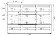
도 5는 하나의 이미지를 다른 타일 크기로 분할하는 타일 맵핑의 예를 보여준다. 도 5를 참조하면, 이미지(500)의 수평으로 분할되는 타일들의 수와 맵핑 메모리(200)의 뱅크 수가 동일한 경우를 보여준다.FIG. 5 shows an example of tile mapping for dividing one image into different tile sizes. Referring to FIG. 5, the number of tiles horizontally divided by the
사이즈 (256×128)의 이미지(500)에서 타일 사이즈가 (64×32)인 경우, 도시된 바와 같이 이미지(500) 상에서 동일 열에 위치하는 타일들(①, ⑤, ⑨, ⑬)은 동일한 뱅크에 맵핑된다. 따라서, 이미지(500) 상에서 특정 영역이 선택되었을 때, 동일 뱅크의 서로 다른 행을 액세스해야하는 오픈-로-액세스 문제가 발생할 확률이 다분하다. 예를 들면, 유저에 의해서 이미지 영역(510)이 선택되면, 맵핑 메모리(200)로부터 이미지 영역(510)에 대응하는 픽셀 데이터를 읽기 위해서는 뱅크2(Bank2) 및 뱅크3(Bank3)에 액세스해야 한다. 타일들(⑪, ⑮)에 대응하는 픽셀 데이터를 읽을 경우에, 맵핑 메모리(200)의 뱅크2(Bank2)에서 서로 다른 행들을 액세스해야 함을 의미한다. 이것은 타일 맵핑 모드에서 오픈-로-액세스 오버헤드가 불가피함을 의미한다.The tiles (①, ⑤, ⑨, ⑬) located in the same column on the
도 6은 타일 맵핑 모드에서 발생하는 문제를 해결하기 위한 방법을 간략히 보여주는 도면이다. 즉, 도 6은 도 2의 어드레스 변환기(122)에서 수행되는 뱅크 플립핑(Bank Flipping) 연산을 간략히 보여주는 블록도이다.6 is a diagram briefly showing a method for solving a problem occurring in a tile mapping mode. That is, FIG. 6 is a block diagram briefly showing a bank flipping operation performed in the
도 6을 참조하면, 각각의 타일들이 할당되는 뱅크들의 어드레스 (0, 1, 2, 3)가 타일 맵핑 모드에 대해서 도시되어 있다. 여기서 뱅크 어드레스는 설명의 편의를 위하여 10진 수로 나타내었다. 타일 맵핑 모드에서는, 이미지상에서 동일 열에 위치하는 타일들은 동일 뱅크들에 할당된다. 예를 들면, 첫 번째 열에 위치하는 타일들에 할당되는 뱅크 어드레스는 모두 0이다. 그리고 두 번째 열에 위치하는 타일들이 할당받는 뱅크 어드레스는 모두 1이다. 따라서, 타일 맵핑 모드에서는 오픈-로-액세스가 발생할 확률이 높다.Referring to FIG. 6, the addresses (0, 1, 2, 3) of the banks to which each tile is assigned are shown for the tile mapping mode. Here, the bank addresses are represented by decimal numbers for convenience of explanation. In the tile mapping mode, tiles located in the same column on the image are assigned to the same banks. For example, the bank addresses allocated to the tiles located in the first column are all zero. And the tiles located in the second column are all assigned bank addresses. Thus, there is a high probability that open-to-access will occur in the tile mapping mode.
상술한 상태에서, 본 발명의 어드레스 변환기(122, 도 2 참조)는 뱅크 플립핑 연산을 실행한다. 이미지 상에서 인접한 타일들은 서로 다른 뱅크 어드레스를 할당받도록 뱅크 어드레스를 특정 규칙에 따라 재할당하는 것이 뱅크 플립핑 연산이다. 뱅크 플립핑 연산을 위하여, 이미지 상에서 짝수 행에 대응하는 타일들의 뱅크 어드레스만 재할당하면 된다. 여기서, 짝수 행들의 타일들에 대해서 뱅크 플립핑 연산이 실시되는 것으로 설명되었으나, 본 발명은 이에 국한되지 않는다. 즉, 홀수 행들에 대응하는 타일들에 대해서만 뱅크 플립핑 연산이 수행될 수도 있다.In the above-described state, the address converter 122 (see Fig. 2) of the present invention executes the bank flip operation. It is a bank flip operation to reallocate the bank addresses according to a specific rule so that adjacent tiles on the image are assigned different bank addresses. For the bank flip operation, only the bank addresses of the tiles corresponding to the even rows in the image are reallocated. Here, it is described that the bank flipping operation is performed on the tiles of even rows, but the present invention is not limited to this. That is, the bank flip operation may be performed only on tiles corresponding to odd rows.
이러한 조작은 각각의 타일들이 할당되는 뱅크 어드레스의 최상위 비트(MSB)를 토글링하는 것으로 구현될 수 있다. 즉, 타일 맵핑 모드에서 '00'의 뱅크로 할당된 타일은 '10'의 뱅크로 그 할당이 전환된다. 타일 맵핑 모드에서 '01'의 뱅크로 할당된 타일은 '11'의 뱅크로 그 할당이 전환된다. 타일 맵핑 모드에서 '10'의 뱅크로 할당된 타일은 '00'의 뱅크로 그 할당이 전환된다. 타일 맵핑 모드에서 '11'의 뱅크로 할당된 타일은 '01'의 뱅크로 그 할당이 전환된다.This operation may be implemented by toggling the most significant bit (MSB) of the bank address to which each tile is assigned. That is, in the tile mapping mode, the tiles allocated to the bank of '00' are switched to the bank of '10 '. In the tile mapping mode, the tiles allocated to the bank of '01' are switched to the banks of '1 1'. In the tile mapping mode, the tiles allocated to the bank of '10' are switched to the bank of '0 0'. In the tile mapping mode, the tiles allocated to the bank of '11' are switched to the bank of '0 1'.
결과적으로, 타일 맵핑 모드에서 (0, 1, 2, 3)으로 뱅크 어드레스를 할당받은 타일들은 뱅크 플립핑 연산에 의해서 (2, 3, 0, 1)의 뱅크 어드레스로 변환된다. 따라서, 상호 인접하는 타일들 간에 동일한 뱅크에 어드레스가 할당되는 경우가 방지될 수 있다.As a result, tiles assigned bank addresses in (0, 1, 2, 3) in the tile mapping mode are converted into bank addresses of (2, 3, 0, 1) by the bank flip operation. Thus, it can be prevented that addresses are assigned to the same bank among mutually adjacent tiles.
도 7은 타일 맵핑 모드에서 뱅크 플립 맵핑 모드로 전환되었을 때의 효과를 보여주기 위한 블록도이다. 도 7을 참조하면, 타일 맵핑 모드에서는 이미지(600) 상에서 선택 영역(610)을 액세스하기 위해서는 동일 뱅크에서 서로 다른 행을 선택 해야 경우가 불가피하였다. 즉, 선택 영역(610)에 해당하는 데이터를 맵핑 메모리(200)에서 액세스하면, 타일들(⑪, ⑮)이 할당된 뱅크2(BANK2)의 서로 다른 행들을 액세스해야 한다.7 is a block diagram showing an effect of switching from the tile mapping mode to the bank flip mapping mode. Referring to FIG. 7, in the tile mapping mode, it is inevitable to select different rows in the same bank in order to access the
하지만, 뱅크 플립(BF) 모드로 어드레스가 변환되는 경우에는 맵핑 메모리(200)에 저장된 이미지(700) 상에서 선택 영역(710, 720)은 모두 다른 뱅크들에 할당되게 된다. 즉, 선택 영역의 일부(710)는 뱅크들(Bank2, Bank3)에 할당되고, 다른 일부(720)는 뱅크들(Bank0, Bank1)에 할당된다. 따라서, 선택 영역을 읽기 위해서 맵핑 메모리(200)에 액세스하더라도 동일 뱅크의 서로 다른 페이지들을 읽어야 하는 확률은 대폭 감소하게 된다.However, when the address is converted in the bank flip (BF) mode, the
이하에서는 동일 열에 동일 뱅크가 맵핑되는 경우를 방지하기 위해 뱅크 어드레스를 리맵핑하는 동작을 뱅크 인터리빙(Bank Interleaving)이라 칭하기로 한다. 타일 맵핑 모드(TM Mode)에서는 이미지 상에서 인접한 타일들의 픽셀 데이터가 맵핑 메모리(200, 도 1 참조)의 동일 뱅크에 저장될 수 있다. 즉, 이미지 상에서 동일 열에 포함되는 인접한 두 개의 타일이 맵핑 메모리(200)의 동일 뱅크에 할당되면 오픈-로-액세스가 발생할 확률이 높다.Hereinafter, the operation of remapping the bank address in order to prevent the same bank from being mapped to the same column will be referred to as bank interleaving. In the tile mapping mode (TM Mode), pixel data of adjacent tiles on the image can be stored in the same bank of the mapping memory 200 (see FIG. 1). That is, if two adjacent tiles included in the same column on the image are allocated to the same bank of the
이 경우에, 뱅크 플립 맵핑 모드(BF Mode)로 뱅크 어드레스를 변환하여 문제의 개선이 가능하다. 이미지 상에서 짝수 행들이나 또는 홀수 행들에 위치하는 타일들의 뱅크 어드레스가 플립핑(Flipping)되면, 뱅크 인터리빙(Bank Interleaving: BI)이 발생한다. 따라서, 이미지의 특정 영역을 처리하기 위하여 맵핑 메모리(200)에 액세스할 때, 동일 뱅크의 서로 다른 페이지를 연속해서 액세스해야 하는 확률 이 감소된다.In this case, the problem can be solved by converting the bank address in the bank flip mapping mode (BF Mode). Bank interleaving (BI) occurs when the bank addresses of tiles located on even or odd rows in the image are flipped. Thus, when accessing the
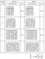
도 8은 타일 맵핑 또는 뱅크 플립 맵핑 모드에서 타일 수에 따른 뱅크 인터리빙(BI)의 정도를 보여주기 위한 표이다. 도 8을 참조하면, 뱅크 인터리빙의 정도는 타일, 이미지의 크기, 그리고 맵핑 메모리(200)의 페이지 사이즈에 따라서 상대적인 값으로 나타난다.8 is a table showing the degree of bank interleaving (BI) according to the number of tiles in the tile mapping or bank flip mapping mode. Referring to FIG. 8, the degree of bank interleaving is represented by a value relative to a tile, an image size, and a page size of the
이미지의 타일에 대한 상대적인 크기를 나타내는 인수(Factor) T는 이미지와 타일의 사이즈, 그리고 맵핑 메모리(200)의 페이지 사이즈와 관련된 값이다. T 값은 아래의 수학식 1로 정의될 수 있다.Factor T, which indicates the relative size of the image to the tile, is a value associated with the size of the image, tile, and page size of the

(단, ImgH는 이미지의 수평 사이즈, TileV는 타일의 수직 사이즈, Page Size는 맵핑 메모리의 페이지 사이즈를 나타낸다.)(Where ImgH is the horizontal size of the image, TileV is the vertical size of the tile, Page Size is the page size of the mapping memory).
설명의 편의를 위하여, 타일 사이즈가 (64×32), 맵핑 메모리(200)는 4개 뱅크 구조이며, 각 페이지들의 사이즈는 2KByte 구조로 가정한다. 그러면, T 값은 이미지의 하나의 행에 포함되는 타일의 수에 해당한다.For convenience of explanation, the tile size is (64 x 32), the
도면을 참조하여, T 값이 4인 경우를 살펴보자. 이 경우, 타일 맵핑 모드(TM Mode)에서는 이미지 상에서 동일 열에 인접한 타일들은 모두 동일한 뱅크에 맵핑되는 것으로 나타나 있다. 각 타일들 내부에 기재된 수는 맵핑되는 뱅크 어드레스를 나타낸다. 따라서, 오픈-로-액세스와 같은 문제가 발생할 확률이 매우 높다. 그리고 뱅크 인터리빙(BI)의 정도는 직관적으로도 최악(Worst)임을 인지할 수 있다.Referring to the drawings, let us consider a case where the T value is 4. In this case, in the tile mapping mode (TM Mode), tiles adjacent to the same column on the image are all mapped to the same bank. The number written within each tile represents the bank address to be mapped. Thus, there is a high probability that problems such as open-access will occur. And the degree of bank interleaving (BI) is intuitively worst (Worst).
반면에, T 값이 4인 뱅크 플립 맵핑 모드(BF Mode)에서는 어느 하나의 타일도 인접한 타일들이 동일한 뱅크에 맵핑된 것이 존재하지 않는다. 따라서, 오픈-로-액세스와 같은 문제가 발생할 확률이 현저히 낮다. 뱅크 인터리빙(BI)의 정도는 직관적으로도 최상(Best)임을 알 수 있다.On the other hand, in a bank flip mapping mode (BF Mode) with a T value of 4, no tile has adjacent tiles mapped to the same bank. Therefore, the probability of problems such as open-to-access is significantly lower. The degree of bank interleaving (BI) is intuitively the best.
T 값이 5인 경우, 즉 이미지의 하나의 행에 수용가능한 타일의 수가 5개인 경우를 살펴보자. 이 경우, 타일 맵핑 모드(TM Mode)에서는 T 값이 4인 때보다는 높은 뱅크 인터리빙 정도를 가지는 것을 볼 수 있다. 하지만, 맵핑되는 뱅크 어드레스가 대각선 방향으로 동일한 타일들이 존재한다. 따라서, T 값이 5인 때의 타일 맵핑 모드에서는 T 값이 4일 때보다는 뱅크 인터리빙의 정도가 향상되었다. 하지만, T 값이 5인 때의 타일 맵핑 모드에서는 개선의 여지가 여전히 존재한다. 또한, T 값이 5인 뱅크 플립 맵핑 모드(BF Mode)에서는, 타일 맵핑 모드와 유사한 정도의 뱅크 인터리빙(BI) 정도를 시각적으로 확인할 수 있다.Let's look at a case where the T value is 5, that is, the number of acceptable tiles in one row of the image is five. In this case, it can be seen that the tile mapping mode (TM Mode) has a higher degree of bank interleaving than that of T = 4. However, there are tiles in which the mapped bank addresses are diagonally identical. Therefore, in the tile mapping mode when the T value is 5, the degree of bank interleaving is improved as compared to when the T value is 4. However, there is still room for improvement in the tile mapping mode when the T value is 5. Further, in the bank flip mapping mode (BF Mode) in which the T value is 5, the degree of bank interleaving (BI) similar to the tile mapping mode can visually be confirmed.
T 값이 6인 경우, 즉 이미지의 하나의 행에 수용가능한 타일의 수가 6개인 경우를 살펴보자. 이 경우, 타일 맵핑 모드(TM Mode)에서는 어느 하나의 타일도 인접한 타일들이 동일한 뱅크에 맵핑된 것이 존재하지 않는다. 따라서, 오픈-로-액세스와 같은 문제가 발생할 확률이 현저히 낮다. 뱅크 인터리빙(BI)의 정도는 직관적으로도 최상(Best)임을 알 수 있다. 반면에, T 값이 6인 경우의 뱅크 플립 맵핑 모드(BF Mode)에서는, 이미지 상에서 동일 열에 인접한 타일들이 모두 동일한 뱅크에 맵핑되는 것으로 나타나 있다. 따라서, 뱅크 인터리빙(BI)의 정도는 직관적으로도 최악(Worst)임을 인지할 수 있다.Let's look at a case where the T value is 6, that is, the number of tiles that can be accommodated in one row of the image is 6. In this case, in the tile mapping mode (TM Mode), there is no one tile in which adjacent tiles are mapped to the same bank. Therefore, the probability of problems such as open-to-access is significantly lower. The degree of bank interleaving (BI) is intuitively the best. On the other hand, in the bank flip mapping mode (BF Mode) when the T value is 6, all tiles adjacent to the same column on the image are shown to be mapped to the same bank. Therefore, it can be recognized that the degree of bank interleaving (BI) is intuitively worst.
T 값이 7인 경우, 즉 이미지의 하나의 행에 수용가능한 타일의 수가 7개인 경우를 살펴보자. 이 경우, 타일 맵핑 모드(TM Mode)에서는 T 값이 6인 때보다는 낮은 뱅크 인터리빙(BI) 정도를 가지는 것을 볼 수 있다. 즉, 타일들의 맵핑되는 뱅크 어드레스가 대각선 방향으로 동일하다. 따라서, T 값이 7인 때의 타일 맵핑 모드에서는 T 값이 6일 때보다는 뱅크 인터리빙(BI)의 정도가 악화되었다. 또한, T 값이 7인 경우의 뱅크 플립 맵핑 모드(BF Mode)에서는, 타일 맵핑 모드와 유사한 정도의 뱅크 인터리빙(BI) 정도를 나타냄을 시각적으로 확인할 수 있다.Consider a case where the T value is 7, i.e., the number of acceptable tiles in one row of the image is 7. In this case, it can be seen that the tile mapping mode (TM Mode) has a lower level of bank interleaving (BI) than a case where the T value is 6. That is, the mapped bank addresses of the tiles are diagonally the same. Therefore, in the tile mapping mode when the T value is 7, the degree of bank interleaving (BI) is worse than when the T value is 6. In addition, in the bank flip mapping mode (BF Mode) when the T value is 7, it is visually confirmed that the degree of bank interleaving (BI) is similar to that of the tile mapping mode.
이상에서는, 이미지 사이즈에 따른 타일 맵핑 모드(TM Mode)와 뱅크 플립 맵핑 모드(BF Mode)의 뱅크 인터리빙 정도를 표를 통해서 살펴보았다. 결론적으로, 뱅크 인터리빙(BI)은 타일 맵핑 모드(TM Mode)와 뱅크 플립 맵핑 모드(BF Mode) 각각에 상보적인 크기로 나타남을 알 수 있다. 즉, 뱅크 인터리밍(BI)은 이미지, 타일, 맵핑 메모리(200)의 페이지의 사이즈에 따라서 타일 맵핑 모드(TM Mode)에서 더 바람직할 수도 있고, 뱅크 플립 맵핑 모드(BF Mode)에서 더 바람직할 수도 있다.In the above, the bank interleaving degree of the tile mapping mode (TM mode) and the bank flip mapping mode (BF mode) according to the image size is shown in the table. As a result, it can be seen that the bank interleaving (BI) is a complementary size to the tile mapping mode (TM mode) and the bank flip mapping mode (BF mode), respectively. That is, the bank interleaving BI may be more preferable in the tile mapping mode (TM Mode) depending on the size of the page of the image, the tile, and the
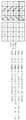
도 9a 및 도 9b는 뱅크 인터리빙(BI)의 크기를 수치로 정량화하기 위한 방법을 보여주는 도면들이다. 하나의 이미지에 대한 뱅크 인터리빙(BI)의 크기를 수치로 정량화한 값을 매트릭(Metric)이라 칭하기로 한다. 도 9a 및 도 9b는 도 8의 T 값이 4인 경우, 타일 맵핑 모드(TM Mode)와 뱅크 플립 맵핑 모드(BF Mode) 각각에 대한 매트릭(Metric)을 계산하는 과정을 보여준다.9A and 9B are diagrams showing a method for quantifying the size of the bank interleaving (BI) by numerical values. A value obtained by quantifying the size of the bank interleaving (BI) for one image with a numerical value will be referred to as a metric. FIGS. 9A and 9B show a process of calculating a metric for each of the tile mapping mode (TM Mode) and the bank flip mapping mode (BF Mode) when the T value is 4 in FIG.
우선, 어느 하나의 이미지에 포함되는 전체 타일들의 뱅크 인터리빙의 척도가 되는 매트릭(Metric)을 구하는 방법이 아래 수학식 2로 정의될 수 있다.First, a method for obtaining a metric that is a measure of bank interleaving of all tiles included in one image can be defined by the following equation (2).


(단, i는 이미지의 행, j는 이미지의 열)(Where i is the row of the image and j is the column of the image)
매트릭(Metric)을 구하기 위해서는 이미지에 포함되는 타일들 각각의 비교값(Compare)를 구해야 한다. 어느 하나의 타일에 대한 비교값(Compare)은 인접하는 타일들이 맵핑되는 뱅크 어드레스가 어느 하나의 타일과 동일한지 여부에 따라서 결정된다. 타일들에 대한 비교값들(Compare)이 도출되면, 전체 타일들의 비교값들을 합하고 평균을 구함으로써 매트릭(Metric)이 구해진다.In order to obtain a metric, a comparison value of each tile included in the image should be obtained. A comparison value for any one tile is determined according to whether the bank address to which adjacent tiles are mapped is the same as any one tile. When the comparison values for the tiles are derived, a metric is obtained by adding the comparison values of all the tiles and averaging the comparison values.
도면을 참조하여, 매트릭을 구하는 방법을 타일 맵핑 모드와 뱅크 플립 맵핑 모드들 각각에 대해서 설명하기로 한다. 도 9a를 참조하면, 타일 맵핑 모드(TM Mode)에서 1행 1열에 대응하는 타일의 비교값(Compare)은 1행 1열에 대응하는 타일의 뱅크 어드레스와 인접한 (1, 2), (2, 1), (2, 2)의 타일들 간의 뱅크 어드레스의 비교값들을 합산함으로써 구해진다. 즉, 어느 하나의 타일의 비교값(Compare)은 인접한 타일과 동일한 뱅크 어드레스이면 비교값은 0, 다른 뱅크 어드레스이면 1을 할당하여 합산해서 구한다.Referring to the drawings, a method of obtaining a matrix will be described for each of a tile mapping mode and a bank flip mapping mode. 9A, a comparison value (Compare) of a tile corresponding to the first row and the first column in the tile mapping mode (TM Mode) is (1, 2), (2, 1 ), And (2, 2), respectively. That is, if the comparison value Compare of any one tile is the same bank address as the adjacent tile, the comparison value is 0 and the other bank address is assigned 1, and are summed.
즉, 1행 1열에 대응하는 타일의 비교값(Compare)은 3개의 인접한 타일들과 비교하여 (1+0+1= 2)이라는 결과를 얻게 된다. 1행 2열에 대응하는 타일의 비교값(Compare)은 5개의 인접 타일들과의 비교값의 합(1+1+0+1+1= 4)으로 산출된다. 1행 3열에 대응하는 타일의 비교값(Compare)은 5개의 인접 타일들과의 비교값의 합(1+1+0+1+1= 4)으로 산출된다. 1행 4열에 대응하는 타일의 비교값(Compare)은 3개의 인접한 타일들과 비교하여 (1+0+1= 2)이라는 결과를 얻게 된다. 결과적으로, 1행의 타일들 각각의 비교값은 (2, 4, 4, 2)로 계산된다. 동일한 방식으로, 2행 및 3행의 비교값은 각각 (3, 6, 6, 3), 4행의 타일들 각각의 비교값은 (2, 4, 4, 2)로 계산된다.That is, the comparison value (Compare) of the tiles corresponding to the first row and the first column is (1 + 0 + 1 = 2) compared with the three adjacent tiles. The comparison value (Compare) of the tiles corresponding to the first row and the second column is calculated as the sum (1 + 1 + 0 + 1 + 1 = 4) of the comparison values with the five adjacent tiles. The comparison value (Compare) of the tiles corresponding to the first row and third column is calculated as the sum (1 + 1 + 0 + 1 + 1 = 4) of the comparison values with the five adjacent tiles. A comparison value of tiles corresponding to the first row and fourth column is compared with three adjacent tiles to obtain (1 + 0 + 1 = 2). As a result, the comparison value of each of the tiles in a row is calculated as (2, 4, 4, 2). In the same manner, the comparison values of the second row and the third row are respectively (3, 6, 6, 3) and the comparison values of the tiles of the fourth row are calculated as (2, 4, 4, 2).
타일들 각각의 비교값들을 합하면 60이 되고, 이 값을 전체 타일의 수(16)로 나누면 매트릭(Metric)으로 3.8이라는 값이 산출된다. 따라서, 타일 맵핑 모드(TM Mode)에서 매트릭(Metric)은 3.8이라는 상대적인 뱅크 인터리빙 크기를 가진다고 볼 수 있다.The sum of the comparison values of each tile is 60, and dividing this value by the total number of tiles (16) yields a value of 3.8 as a metric. Therefore, in the tile mapping mode (TM Mode), the metric has a relative bank interleaving size of 3.8.
도 9b를 참조하면, 뱅크 플립 맵핑 모드(BF Mode)에서 1행 1열에 대응하는 타일의 비교값(Compare)은 1행 1열에 대응하는 타일의 뱅크 어드레스와 인접한 (1, 2), (2, 1), (2, 2)의 타일들 간의 뱅크 어드레스의 비교값들을 합산함으로써 구해진다. 즉, 어느 하나의 타일의 비교값(Compare)은 인접한 타일과 동일한 뱅크 어드레스이면 비교값은 0, 다른 뱅크 어드레스이면 1을 할당하여 합산해서 구한다.9B, a comparison value (Compare) of the tiles corresponding to the first row and the first column in the bank flip mapping mode (BF Mode) is (1, 2), (2, 1), and (2, 2). That is, if the comparison value Compare of any one tile is the same bank address as the adjacent tile, the comparison value is 0 and the other bank address is assigned 1, and are summed.
즉, 1행 1열에 대응하는 타일의 비교값(Compare)은 3개의 인접한 타일들과 비교하여 (1+1+1= 3)이라는 결과를 얻게된다. 1행 2열에 대응하는 타일의 비교값(Compare)은 5개의 인접 타일들과의 비교값의 합(1+1+1+1+1= 5)으로 산출된다. 1행 3열에 대응하는 타일의 비교값(Compare)은 5개의 인접 타일들과의 비교값의 합(1+1+1+1+1= 5)으로 산출된다. 1행 4열에 대응하는 타일의 비교값(Compare)은 3개의 인접한 타일들과 비교하여 (1+1+1= 3)이라는 결과를 얻게된다. 결과적으로, 1행의 타일들 각각의 비교값은 (3, 5, 5, 3)로 계산된다. 동일한 방식으로, 2행 및 3행의 비교값은 각각 (5, 8, 8, 5), 4행의 타일들 각각의 비교값은 (3, 5, 5, 3)로 계산된다. 뱅크 플립 맵핑 모드(BF Mode)에서는 어느 하나의 타일도 인접한 타일 과 동일한 뱅크에 맵핑되지 않는다.That is, the comparison value (Compare) of the tiles corresponding to the first row and the first column is (1 + 1 + 1 = 3) compared with three adjacent tiles. The comparison value (Compare) of the tiles corresponding to the first row and the second column is calculated as the sum (1 + 1 + 1 + 1 + 1 = 5) of the comparison values with the five adjacent tiles. The comparison value (Compare) of the tiles corresponding to the first row and the third column is calculated as the sum (1 + 1 + 1 + 1 + 1 = 5) of the comparison values with the five adjacent tiles. The comparison value of the tile corresponding to the first row and fourth column is (1 + 1 + 1 = 3) compared with the three neighboring tiles. As a result, the comparison value of each of the tiles in a row is calculated as (3, 5, 5, 3). In the same manner, the comparison values of the second row and the third row are calculated as (5, 8, 8, 5), and the comparison values of the tiles of the fourth row are calculated as (3, 5, 5, 3). In the bank flip mapping mode (BF Mode), no tile is mapped to the same bank as the adjacent tile.
타일들 각각의 비교값들을 합하면 84가 되고, 이 값을 전체 타일의 수(16)로 나누면 매트릭(Metric)으로 5.3이라는 값이 산출된다. 따라서, 뱅크 플립 맵핑 모드(BF Mode)에서 매트릭(Metric)은 5.3의 뱅크 인터리빙 크기를 가진다고 볼 수 있다. 이것은 타일 맵핑 모드(TM Mode)의 3.8에 비하여 상대적으로 크므로, 뱅크 플립 맵핑 모드로 어드레스 변환을 수행하는 것이 바람직함을 의미한다.When the comparison values of the respective tiles are added, the value becomes 84, and dividing this value by the total number of tiles (16) yields a value of 5.3 as a metric. Therefore, in the bank flip mapping mode (BF Mode), the metric has a bank interleaving size of 5.3. This is relatively large compared to 3.8 of the tile mapping mode (TM Mode), which means that it is desirable to perform address translation in the bank flip mapping mode.
도 10 내지 도 11은 다양한 조건에서 T 값에 대한 매트릭(Metric) 값의 변화를 보여주는 그래프들이다. 도 10은 4개 뱅크(4-Bank), 2KByte 구조의 맵핑 메모리에서 타일 맵핑 모드(TM Mode)와 뱅크 플립 맵핑 모드(BF Mode) 각각의 매트릭(Metric) 값들을 보여준다. 점선으로 도시된 타일 맵핑 모드(TM Mode)의 매트릭(Metric)은 T 값이 (1, 3), (5, 7), (9, 11)에 분포하는 구간에서 뱅크 플립 맵 핑 모드(BF Mode)보다 높다. 따라서, 4개 뱅크(4-Bank), 2KByte 구조의 맵핑 메모리를 사용하는 경우, T 값이 (1, 3), (5, 7), (9, 11)에 분포하는 경우, 타일 맵핑 모드로 어드레스 맵핑을 수행하면 액세스 성능을 높일 수 있다.10 to 11 are graphs showing the change of the metric value for the T value under various conditions. FIG. 10 shows metric values of a tile mapping mode (TM Mode) and a bank flip mapping mode (BF Mode) in a mapping memory having a 4-bank (4-bank) structure and a 2-KByte structure. The metric of the tile mapping mode (TM Mode) indicated by the dotted line indicates the bank flip mapping mode (BF Mode) in the interval where the T value is distributed to (1, 3), (5, 7) ). Therefore, when a mapping memory having a 4-bank (4-bank) structure and a 2-KByte structure is used, when the T value is distributed in (1, 3), (5, 7) Address mapping can improve access performance.
반면, 4개 뱅크(4-Bank), 2KByte 구조의 맵핑 메모리에서 실선으로 도시된 뱅크 플립 맵핑 모드(BF Mode)에서의 매트릭(Metric)은 T 값이 (3, 5), (7, 9), (11, 13)에 분포하는 구간에서 상대적으로 뱅크 플립 맵핑 모드(BF Mode)보다 높다. 따라서, 4개 뱅크(4-Bank), 2KByte 구조의 맵핑 메모리를 사용하는 경우, T 값이 (3, 5), (7, 9), (11, 13)에 분포하는 경우, 타일 맵핑 모드를 뱅크 플립 맵핑 모드로 변환하는 것이 바람직하다.On the other hand, the metric in the bank flip mapping mode (BF Mode) shown by the solid line in the mapping memory of the 4-bank (4-bank) , And (11, 13) are relatively higher than the bank flip mapping mode (BF Mode). Therefore, in the case of using 4-bank (4-bank) and 2-KByte mapping memory, if the T value is distributed in (3, 5), (7, 9) It is preferable to switch to the bank flip mapping mode.
도 11은 8개 뱅크(8-Bank), 4KByte 구조의 맵핑 메모리에서 타일 맵핑 모드(TM Mode)와 뱅크 플립 맵핑 모드(BF Mode) 각각의 매트릭(Metric) 값들을 보여준다. 점선으로 도시된 타일 맵핑 모드(TM Mode)의 매트릭(Metric)은 T 값이 (2, 6), (10, 14)에 분포하는 구간에서 뱅크 플립 맵핑 모드(BF Mode)보다 높다. 따라서, 8개 뱅크(8-Bank), 4KByte 구조의 맵핑 메모리를 사용하는 경우, T 값이 (2, 6), (10, 14)에 분포하는 경우, 타일 맵핑 모드(TM Mode)로 어드레스 맵핑을 수행하면 액세스 성능을 높일 수 있다.FIG. 11 shows the metric values of the tile mapping mode (TM Mode) and the bank flip mapping mode (BF Mode) in the 8-bank (8-bank) and 4-KByte structure mapping memory, respectively. The metric of the tile mapping mode (TM Mode) shown by the dotted line is higher than the bank flip mapping mode (BF Mode) in the interval where the T value is distributed to (2, 6), (10, 14). Therefore, when the mapping memory having 8 banks (8-bank) and 4 KByte structure is used, when the T value is distributed to (2, 6), (10, 14) Can improve access performance.
반면, 8개 뱅크(8-Bank), 4KByte 구조의 맵핑 메모리에서 실선으로 도시된 뱅크 플립 맵핑 모드(BF Mode)에서의 매트릭(Metric)은 T 값이 (6, 10), (14, 18)에 분포하는 구간에서 상대적으로 뱅크 플립 맵핑 모드(BF Mode)보다 높다. 따라서, 4개 뱅크(8-Bank), 4KByte 구조의 맵핑 메모리를 사용하는 경우, T 값이 (6, 10), (14, 18)에 분포하는 경우, 타일 맵핑 모드(TM Mode)를 뱅크 플립 맵핑 모드(BF Mode)로 변환하는 것이 바람직하다.On the other hand, the metrics in the bank flip mapping mode (BF Mode) shown by the solid line in the mapping memory of the 8-bank (8-bank) and 4-kbyte structures have T values of (6, 10) Is relatively higher than the bank flip mapping mode (BF Mode). Therefore, when the mapping memory having four banks (8-Bank) and 4-KByte structure is used, when the T value is distributed to (6, 10) and (14, 18), the tile mapping mode Mapping mode (BF Mode).
여기서, 입력되는 특정 이미지 사이즈에서 타일 맵핑 모드(TM Mode)와 뱅크 플립 맵핑 모드(BF Mode) 중 어느 방식이 바람직한지를 결정하는 도 2의 검출기(124)의 기능을 보다 자세히 설명하기로 한다. 검출기(124)는 입력되는 이미지 데이터를 참조하여, T 값의 범위가 뱅크 플립 맵핑 모드(BF Mode)에 해당하는지, 또는 타일 맵핑 모드(TM Mode)에 해당하는지를 판단한다. 검출기(124)의 판단은 아래 수학식 3에 의거하여 수행된다.Here, the function of the

(# Banks는 맵핑 메모리의 뱅크 수, n은 임의의 자연수)(# Banks is the number of banks of the mapping memory, and n is an arbitrary natural number)
상술한 수학식 3의 조건에 일치하는 경우, 검출기(124)는 뱅크 플립 맵핑 모드(BF Mode)로 맵핑 메모리의 어드레스를 출력하도록 어드레스 변환기(122) 및 어드레스 선택부(123)를 제어한다.The
따라서 본 발명의 실시 예에 의한 어드레스 맵핑 방식에 따르면, 이미지의 사이즈와 맵핑 메모리의 구조에 최적화된 맵핑 모드를 선택할 수 있다. 그리고 본 발명의 실시 예에 따른 뱅크 인터리빙 방법에 의하면, 임의의 조건에서 적응적으로 뱅크 어드레스를 변환하여 최적의 액세스 성능의 보장이 가능하다.Therefore, according to the address mapping method according to the embodiment of the present invention, a mapping mode optimized for the size of the image and the structure of the mapping memory can be selected. According to the bank interleaving method according to the embodiment of the present invention, it is possible to adaptively perform bank address conversion under arbitrary conditions to ensure optimum access performance.
이상에서는 이미지 데이터를 맵핑 메모리에 저장하는 기술을 통해서 본 발명 의 사상이 기술되었다. 그러나 본 발명의 이점은 여기에만 국한되지 않는다. 임의의 데이터를 복수의 뱅크를 가지는 메모리에 저장하는 모든 저장 장치에 확대 적용이 가능하다.The idea of the present invention has been described above by means of a technique of storing image data in a mapping memory. However, the advantages of the present invention are not limited thereto. It is possible to apply the present invention to all storage devices that store arbitrary data in a memory having a plurality of banks.
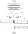
도 12는 본 발명의 실시 예에 따른 선택적 및 적응적으로 뱅크 어드레스를 플립핑하는 이미지 데이터의 맵핑 방법을 보여주는 순서도이다. 먼저, 이미지 데이터가 어드레스 발생기(120, 도 2 참조)에 입력되면, 본 발명의 실시 예에 따른 어드레스 맵핑 동작이 시작된다.FIG. 12 is a flowchart illustrating a method of mapping image data for selectively and adaptively flipping bank addresses according to an embodiment of the present invention. Referring to FIG. First, when image data is input to the address generator 120 (see FIG. 2), the address mapping operation according to the embodiment of the present invention starts.
단계 S110에서, 이미지 데이터(Image data)는 어드레스 발생기(120)에 전달된다. 이미지 데이터(Image data)에는 선택된 특정 이미지 영역의 위치(x, y)와 크기 정보(xsize, ysize) 그리고 전체 이미지의 크기 정보(ImgH, ImgV), 타일의 크기 정보(TileH, TileV) 등을 포함할 수 있다. 이 밖에도, 뱅크 플립핑의 필요성을 판단하기 위하여, 시스템-온-칩(SoC) 또는 모듈로 탑재되는 맵핑 메모리(200)의 사양도 더 제공될 수 있다.In step S110, the image data (Image data) is transferred to the
단계 S120에서, 상술한 이미지 데이터를 참조하여 이미지 데이터를 맵핑 메모리(200)에 저장하기 위한 타일 맵핑 어드레스(TM Address)가 생성된다. 타일 맵핑 어드레스(TM Address)는 이미지상의 타일들이 순차적으로 맵핑 메모리 상의 뱅크에 할당되는 뱅크 어드레스 할당 방식이다.In step S120, a tile mapping address (TM Address) for storing the image data in the
단계 S130에서, 검출기(124)는 의하여 뱅크 플립핑이 필요한지를 입력되는 이미지 데이터를 이용하여 계산하고 판단한다. 검출기(124)는 이미지 데이터(Image Data)를 이용하여 해당하는 이미지의 포맷 또는 사이즈에 최적화되는 뱅크 어드레 스의 맵핑 방식을 계산한다. 검출기(124)는 이미지 데이터로부터 이미지의 수평 크기에 수용 가능한 타일의 수(T value)를 계산한다. 검출기(124)는 계산 결과로 출력되는 타일 수(T value)가 타일 맵핑 모드에 대응하는 범위인지, 또는 뱅크 플립 맵핑 모드에 대응하는 범위에 속하는지 판단한다.In step S130, the
단계 S140에서, T 값이 뱅크 플립 맵핑 모드를 적용하기 위한 범위가 아닌 것으로 판단되면, 절차는 단계 S150으로 이동한다. 즉, 단계 S150에서 검출기(124)는 이미 타일 맵핑 어드레스 발생기(121)로부터 출력된 타일 맵핑 어드레스(TM address)를 맵핑 메모리(200)로 제공하도록 어드레스 선택부(123)를 제어한다.If it is determined in step S140 that the T value is not in the range for applying the bank flip mapping mode, the procedure moves to step S150. That is, in step S150, the
반면, 단계 S140에서 T 값이 뱅크 플립 맵핑 모드를 적용하기 위한 타당한 범위로 판단되면, 절차는 단계 S160으로 이동한다.On the other hand, if it is determined in step S140 that the T value is within a reasonable range for applying the bank flip mapping mode, the procedure moves to step S160.
단계 S160에서, 검출기(124)는 어드레스 변환기(122)를 활성화한다. 그러면, 어드레스 변환기(122)는 타일 맵핑 어드레스 발생기(121)로부터 출력된 타일 맵핑 어드레스(TM address)를 뱅크 플립핑을 위해서 재설정한다. 즉, 앞서 설명된 바와 같이, 어드레스 변환기(122)는 이미지상의 짝수 행에 위치하는 타일들의 뱅크 어드레스를 변경한다. 어드레스 변환기(122)는 타일 맵핑 어드레스(TM address) 상에서 짝수 행에 위치하는 타일들의 뱅크 어드레스의 최상위 비트(MSB)를 토글링시킨다. 그러면, 타일들 각각의 뱅크 인터리빙(BI)의 정도는 향상될 수 있다.In step S160, the
단계 S170에서, 검출기(124)는 어드레스 변환기(122)로부터 출력되는 뱅크 플립 맵핑 어드레스(BF Address)를 맵핑 메모리(200)로 제공하도록 어드레스 선택부(123)를 제어한다.The
이상에서와 같이 도면과 명세서에서 최적 실시 예가 개시되었다. 여기서 특정한 용어들이 사용되었으나, 이는 단지 본 발명을 설명하기 위한 목적에서 사용된 것이지 의미 한정이나 특허청구범위에 기재된 본 발명의 범위를 제한하기 위하여 사용된 것은 아니다. 그러므로 본 기술 분야의 통상의 지식을 가진 자라면 이로부터 다양한 변형 및 균등한 타 실시 예가 가능하다는 점을 이해할 것이다. 따라서, 본 발명의 진정한 기술적 보호 범위는 첨부된 특허청구범위의 기술적 사상에 의해 정해져야 할 것이다.As described above, an optimal embodiment has been disclosed in the drawings and specification. Although specific terms have been employed herein, they are used for purposes of illustration only and are not intended to limit the scope of the invention as defined in the claims or the claims. Therefore, those skilled in the art will appreciate that various modifications and equivalent embodiments are possible without departing from the scope of the present invention. Accordingly, the true scope of the present invention should be determined by the technical idea of the appended claims.
도 1은 본 발명의 일 실시 예의 디스플레이 시스템을 보여주는 블록도;1 is a block diagram illustrating a display system of an embodiment of the present invention;
도 2는 도 1에 도시된 어드레스 발생기를 보여주는 블록도;FIG. 2 is a block diagram showing the address generator shown in FIG. 1; FIG.
도 3은 도 1의 맵핑 메모리의 구조를 간략히 보여주는 테이블;FIG. 3 is a table briefly showing the structure of the mapping memory of FIG. 1; FIG.
도 4a 내지 도 4d는 본 발명의 타일 맵핑 모드를 보여주는 도면들;Figures 4A-4D illustrate the tile mapping mode of the present invention;
도 5는 이미지의 수평 성분에 포함되는 타일 수가 증가하는 경우의 타일 맵핑 모드의 예를 보여주는 도면;5 illustrates an example of a tile mapping mode when the number of tiles included in a horizontal component of an image increases;
도 6은 본 발명의 뱅크 플립핑 연산을 보여주는 도면;6 illustrates a bank flip operation of the present invention;
도 7은 타일 맵핑 모드와 뱅크 플립 맵핑 모드를 비교하여 보여주는 도면;FIG. 7 illustrates a comparison between a tile mapping mode and a bank flip mapping mode; FIG.
도 8은 다양한 이미지 포맷에서 타일 맵핑 모드 및 뱅크 플립 맵핑 모드의 뱅크 인터리빙(BI)의 크기를 시각적으로 보여주기 위한 도면;8 is a diagram for visually showing the sizes of bank interleaving (BI) in the tile mapping mode and the bank flip mapping mode in various image formats;
도 9a 및 도 9b는 뱅크 인터리빙의 크기를 정량화하기 위한 매트릭 연산의 방법을 타일 맵핑 모드 및 뱅크 플립 맵핑 모드 각각에 대해서 보여주는 도면들;FIGS. 9A and 9B are diagrams showing a method of a metric calculation for quantifying the size of a bank interleave for each of a tile mapping mode and a bank flip mapping mode; FIG.
도 10 및 도 11은 서로 다른 맵핑 메모리 사양에서 T 값에 따른 매트릭의 변화를 보여주는 그래프들; 그리고Figures 10 and 11 are graphs showing the change of the metric according to the T value in different mapping memory specifications; And
도 12는 본 발명의 실시 예에 따른 어드레스 맵핑 방법을 보여주는 순서도.12 is a flowchart showing an address mapping method according to an embodiment of the present invention;
Claims (10)
Translated fromKoreanPriority Applications (3)
| Application Number | Priority Date | Filing Date | Title |
|---|---|---|---|
| KR1020090134573AKR101639574B1 (en) | 2009-12-30 | 2009-12-30 | Image processing system supplying adaptive bank address and address mapping method thereof |
| US12/903,368US8817033B2 (en) | 2009-12-30 | 2010-10-13 | Method and apparatus for performing adaptive memory bank addressing |
| US14/452,586US9390007B2 (en) | 2009-12-30 | 2014-08-06 | Method and apparatus for performing adaptive memory bank addressing |
Applications Claiming Priority (1)
| Application Number | Priority Date | Filing Date | Title |
|---|---|---|---|
| KR1020090134573AKR101639574B1 (en) | 2009-12-30 | 2009-12-30 | Image processing system supplying adaptive bank address and address mapping method thereof |
Publications (2)
| Publication Number | Publication Date |
|---|---|
| KR20110077894A KR20110077894A (en) | 2011-07-07 |
| KR101639574B1true KR101639574B1 (en) | 2016-07-14 |
Family
ID=44186962
Family Applications (1)
| Application Number | Title | Priority Date | Filing Date |
|---|---|---|---|
| KR1020090134573AActiveKR101639574B1 (en) | 2009-12-30 | 2009-12-30 | Image processing system supplying adaptive bank address and address mapping method thereof |
Country Status (2)
| Country | Link |
|---|---|
| US (2) | US8817033B2 (en) |
| KR (1) | KR101639574B1 (en) |
Families Citing this family (21)
| Publication number | Priority date | Publication date | Assignee | Title |
|---|---|---|---|---|
| US20050131837A1 (en) | 2003-12-15 | 2005-06-16 | Sanctis Jeanne D. | Method, system and program product for communicating e-commerce content over-the-air to mobile devices |
| US8799553B2 (en)* | 2010-04-13 | 2014-08-05 | Apple Inc. | Memory controller mapping on-the-fly |
| JP5884037B2 (en)* | 2011-03-16 | 2016-03-15 | パナソニックIpマネジメント株式会社 | Data processing apparatus, data processing method, and data sharing system |
| KR20130122417A (en)* | 2012-04-30 | 2013-11-07 | 삼성전자주식회사 | Address generator of image processing device and operating method of address generator |
| US9146846B2 (en)* | 2012-09-14 | 2015-09-29 | Advanced Micro Devices, Inc. | Programmable physical address mapping for memory |
| KR101987160B1 (en) | 2012-09-24 | 2019-09-30 | 삼성전자주식회사 | Display driver integrated circuit, display system having the same, and display data processing method thereof |
| CN103680383B (en)* | 2012-09-24 | 2018-09-11 | 三星电子株式会社 | Display driver integrated circuit, display system and method for processing display data |
| US10949876B2 (en) | 2012-10-29 | 2021-03-16 | Overstock.Com, Inc. | System and method for management of email marketing campaigns |
| US9245496B2 (en)* | 2012-12-21 | 2016-01-26 | Qualcomm Incorporated | Multi-mode memory access techniques for performing graphics processing unit-based memory transfer operations |
| US11023947B1 (en) | 2013-03-15 | 2021-06-01 | Overstock.Com, Inc. | Generating product recommendations using a blend of collaborative and content-based data |
| US10810654B1 (en) | 2013-05-06 | 2020-10-20 | Overstock.Com, Inc. | System and method of mapping product attributes between different schemas |
| US10929890B2 (en) | 2013-08-15 | 2021-02-23 | Overstock.Com, Inc. | System and method of personalizing online marketing campaigns |
| US10872350B1 (en)* | 2013-12-06 | 2020-12-22 | Overstock.Com, Inc. | System and method for optimizing online marketing based upon relative advertisement placement |
| US20160299844A1 (en)* | 2015-04-08 | 2016-10-13 | Sandisk Enterprise Ip Llc | Mapping Logical Groups of Data to Physical Locations In Memory |
| KR102491622B1 (en) | 2015-11-17 | 2023-01-25 | 삼성전자주식회사 | Method for operating virtual address generator and method for operating system having the same |
| EP4137940A1 (en)* | 2017-03-20 | 2023-02-22 | Intel Corporation | Systems, methods, and apparatuses for tile matrix multiplication and accumulation |
| WO2019009870A1 (en) | 2017-07-01 | 2019-01-10 | Intel Corporation | Context save with variable save state size |
| US10303398B2 (en)* | 2017-10-26 | 2019-05-28 | Advanced Micro Devices, Inc. | Swizzling in 3D stacked memory |
| US11205179B1 (en) | 2019-04-26 | 2021-12-21 | Overstock.Com, Inc. | System, method, and program product for recognizing and rejecting fraudulent purchase attempts in e-commerce |
| US20210240524A1 (en)* | 2020-01-31 | 2021-08-05 | Qualcomm Incorporated | Methods and apparatus to facilitate tile-based gpu machine learning acceleration |
| KR102565238B1 (en)* | 2021-11-08 | 2023-08-09 | 제주대학교 산학협력단 | Address mapping apparatus and method considering shared memory and cache interleaving |
Citations (2)
| Publication number | Priority date | Publication date | Assignee | Title |
|---|---|---|---|---|
| US20080079744A1 (en) | 2006-06-20 | 2008-04-03 | Via Technologies, Inc. | Systems and Methods for Performing a Bank Swizzle Operation to Reduce Bank Collisions |
| US20090009523A1 (en) | 2006-10-26 | 2009-01-08 | Adrian Philip Wise | System for interleaved storage of video data |
Family Cites Families (14)
| Publication number | Priority date | Publication date | Assignee | Title |
|---|---|---|---|---|
| JPH03203124A (en)* | 1989-12-29 | 1991-09-04 | Hitachi Cable Ltd | Flame-retardant wires and cables |
| GB2277012B (en) | 1993-04-08 | 1997-06-18 | Sony Uk Ltd | Image data storage |
| US5815168A (en) | 1995-06-23 | 1998-09-29 | Cirrus Logic, Inc. | Tiled memory addressing with programmable tile dimensions |
| TW335472B (en)* | 1996-06-20 | 1998-07-01 | Cirus Logic Inc | Method and apparatus for transferring pixel data stored in a memory circuit |
| US5841446A (en) | 1996-11-01 | 1998-11-24 | Compaq Computer Corp. | Method and apparatus for address mapping of a video memory using tiling |
| US6310647B1 (en)* | 1997-04-15 | 2001-10-30 | Eastman Kodak Company | Image format for storing digital images and including multiple application segments |
| US5990912A (en)* | 1997-06-27 | 1999-11-23 | S3 Incorporated | Virtual address access to tiled surfaces |
| US6064407A (en) | 1998-04-30 | 2000-05-16 | Ati Technologies, Inc. | Method and apparatus for tiling a block of image data |
| US6484179B1 (en) | 1999-10-25 | 2002-11-19 | Oracle Corporation | Storing multidimensional data in a relational database management system |
| US6553552B1 (en) | 2000-01-27 | 2003-04-22 | National Semiconductor Corporation | Method of designing an integrated circuit memory architecture |
| JP3918145B2 (en)* | 2001-05-21 | 2007-05-23 | 株式会社ルネサステクノロジ | Memory controller |
| US7016418B2 (en) | 2001-08-07 | 2006-03-21 | Ati Technologies, Inc. | Tiled memory configuration for mapping video data and method thereof |
| US6888551B2 (en)* | 2001-12-07 | 2005-05-03 | Intel Corporation | Sparse refresh of display |
| US20080158601A1 (en)* | 2006-12-29 | 2008-07-03 | Steven Tu | Image memory tiling |
- 2009
- 2009-12-30KRKR1020090134573Apatent/KR101639574B1/enactiveActive
- 2010
- 2010-10-13USUS12/903,368patent/US8817033B2/enactiveActive
- 2014
- 2014-08-06USUS14/452,586patent/US9390007B2/enactiveActive
Patent Citations (2)
| Publication number | Priority date | Publication date | Assignee | Title |
|---|---|---|---|---|
| US20080079744A1 (en) | 2006-06-20 | 2008-04-03 | Via Technologies, Inc. | Systems and Methods for Performing a Bank Swizzle Operation to Reduce Bank Collisions |
| US20090009523A1 (en) | 2006-10-26 | 2009-01-08 | Adrian Philip Wise | System for interleaved storage of video data |
Also Published As
| Publication number | Publication date |
|---|---|
| US8817033B2 (en) | 2014-08-26 |
| US9390007B2 (en) | 2016-07-12 |
| US20110157200A1 (en) | 2011-06-30 |
| US20140347382A1 (en) | 2014-11-27 |
| KR20110077894A (en) | 2011-07-07 |
Similar Documents
| Publication | Publication Date | Title |
|---|---|---|
| KR101639574B1 (en) | Image processing system supplying adaptive bank address and address mapping method thereof | |
| US7805587B1 (en) | Memory addressing controlled by PTE fields | |
| CN100527099C (en) | Enhancing performance of a memory unit of a data processing device by separating reading and fetching functionalities | |
| US8493400B2 (en) | Memory device and memory control for controlling the same | |
| US10163180B2 (en) | Adaptive memory address scanning based on surface format for graphics processing | |
| US7932912B1 (en) | Frame buffer tag addressing for partitioned graphics memory supporting non-power of two number of memory elements | |
| KR100817057B1 (en) | Mapping method and video system for mapping pixel data included in same pixel data group to same bank address of memory | |
| EP0948777A1 (en) | Tiled linear host texture storage | |
| KR102002900B1 (en) | System on chip including memory management unit and memory address translation method thereof | |
| JP3639464B2 (en) | Information processing system | |
| JP2007034304A (en) | Method, graphics controller and image display system for efficiently rotating an image defined by an image matrix wherein each piece of image data corresponds to a particular image row and a particular image column of the image matrix | |
| US20080028151A1 (en) | Cache memory control method and cache memory apparatus | |
| EP3373237A1 (en) | Method and apparatus for scaling down a bayer domain image | |
| KR102516833B1 (en) | Memory apparatus and method for processing data the same | |
| CN104350523A (en) | Padding for multi-channel memory | |
| KR101801901B1 (en) | Memory device accessed in consideration of data locality and electronic system including the same | |
| US8205031B2 (en) | Memory management system and method thereof | |
| US6639603B1 (en) | Hardware portrait mode support | |
| JP2005228073A (en) | Image processing apparatus, microcomputer and electronic apparatus | |
| JP3001763B2 (en) | Image processing system | |
| KR102565238B1 (en) | Address mapping apparatus and method considering shared memory and cache interleaving | |
| US6275243B1 (en) | Method and apparatus for accelerating the transfer of graphical images | |
| EP2550639A1 (en) | Method and integrated circuit for image manipulation | |
| JP5605225B2 (en) | MEMORY CONTROL DEVICE, MEMORY MAPPING METHOD, AND PROGRAM | |
| KR920008266B1 (en) | Memory system for effective analyzation of image |
Legal Events
| Date | Code | Title | Description |
|---|---|---|---|
| PA0109 | Patent application | Patent event code:PA01091R01D Comment text:Patent Application Patent event date:20091230 | |
| PG1501 | Laying open of application | ||
| A201 | Request for examination | ||
| PA0201 | Request for examination | Patent event code:PA02012R01D Patent event date:20141230 Comment text:Request for Examination of Application Patent event code:PA02011R01I Patent event date:20091230 Comment text:Patent Application | |
| E902 | Notification of reason for refusal | ||
| PE0902 | Notice of grounds for rejection | Comment text:Notification of reason for refusal Patent event date:20151113 Patent event code:PE09021S01D | |
| E701 | Decision to grant or registration of patent right | ||
| PE0701 | Decision of registration | Patent event code:PE07011S01D Comment text:Decision to Grant Registration Patent event date:20160530 | |
| GRNT | Written decision to grant | ||
| PR0701 | Registration of establishment | Comment text:Registration of Establishment Patent event date:20160708 Patent event code:PR07011E01D | |
| PR1002 | Payment of registration fee | Payment date:20160711 End annual number:3 Start annual number:1 | |
| PG1601 | Publication of registration | ||
| FPAY | Annual fee payment | Payment date:20190628 Year of fee payment:4 | |
| PR1001 | Payment of annual fee | Payment date:20190628 Start annual number:4 End annual number:4 | |
| PR1001 | Payment of annual fee | Payment date:20200630 Start annual number:5 End annual number:5 | |
| PR1001 | Payment of annual fee | Payment date:20210628 Start annual number:6 End annual number:6 | |
| PR1001 | Payment of annual fee | Payment date:20220622 Start annual number:7 End annual number:7 | |
| PR1001 | Payment of annual fee | Payment date:20230621 Start annual number:8 End annual number:8 | |
| PR1001 | Payment of annual fee | Payment date:20240626 Start annual number:9 End annual number:9 | |
| PR1001 | Payment of annual fee | Payment date:20250624 Start annual number:10 End annual number:10 |