KR101618677B1 - Methods and apparatus for interfacing between a flash memory controller and a flash memory array - Google Patents
Methods and apparatus for interfacing between a flash memory controller and a flash memory arrayDownload PDFInfo
- Publication number
- KR101618677B1 KR101618677B1KR1020117002516AKR20117002516AKR101618677B1KR 101618677 B1KR101618677 B1KR 101618677B1KR 1020117002516 AKR1020117002516 AKR 1020117002516AKR 20117002516 AKR20117002516 AKR 20117002516AKR 101618677 B1KR101618677 B1KR 101618677B1
- Authority
- KR
- South Korea
- Prior art keywords
- flash memory
- edge
- cell
- data
- clock signal
- Prior art date
- Legal status (The legal status is an assumption and is not a legal conclusion. Google has not performed a legal analysis and makes no representation as to the accuracy of the status listed.)
- Expired - Fee Related
Links
Images


Classifications
- G—PHYSICS
- G11—INFORMATION STORAGE
- G11C—STATIC STORES
- G11C16/00—Erasable programmable read-only memories
- G11C16/02—Erasable programmable read-only memories electrically programmable
- G11C16/06—Auxiliary circuits, e.g. for writing into memory
- G11C16/10—Programming or data input circuits
- G—PHYSICS
- G11—INFORMATION STORAGE
- G11C—STATIC STORES
- G11C11/00—Digital stores characterised by the use of particular electric or magnetic storage elements; Storage elements therefor
- G11C11/56—Digital stores characterised by the use of particular electric or magnetic storage elements; Storage elements therefor using storage elements with more than two stable states represented by steps, e.g. of voltage, current, phase, frequency
- G11C11/5621—Digital stores characterised by the use of particular electric or magnetic storage elements; Storage elements therefor using storage elements with more than two stable states represented by steps, e.g. of voltage, current, phase, frequency using charge storage in a floating gate
- G11C11/5628—Programming or writing circuits; Data input circuits
- G—PHYSICS
- G11—INFORMATION STORAGE
- G11C—STATIC STORES
- G11C16/00—Erasable programmable read-only memories
- G11C16/02—Erasable programmable read-only memories electrically programmable
- G11C16/06—Auxiliary circuits, e.g. for writing into memory
- G11C16/34—Determination of programming status, e.g. threshold voltage, overprogramming or underprogramming, retention
- G11C16/3418—Disturbance prevention or evaluation; Refreshing of disturbed memory data
- G11C16/3427—Circuits or methods to prevent or reduce disturbance of the state of a memory cell when neighbouring cells are read or written
Landscapes
- Engineering & Computer Science (AREA)
- Computer Hardware Design (AREA)
- Read Only Memory (AREA)
Abstract
Translated fromKorean
Description
Translated fromKorean관련 출원의 상호 참조Cross reference of related application
본 출원은 본 명세서에 각각 참조로서 포함되어 있는 2008년 7월 1일 출원된 미국 가특허 출원 제 61/133,675호, 2008년 7월 3일 출원된 미국 가특허 출원 제 61/133,921호 및 2008년 7월 10일 출원된 미국 가특허 출원 제 61/134,688호를 우선권 주장한다.This application claims the benefit of U.S. Provisional Patent Application No. 61 / 133,675, filed July 1, 2008, and U.S. Patent Application No. 61 / 133,921, filed July 3, 2008, each of which is incorporated herein by reference. U.S. Provisional Patent Application No. 61 / 134,688, filed July 10, claims priority.
본 출원은 2009년 3월 11일 출원된 발명의 명칭이 "페이지간 섹터, 다중 페이지 코딩 및 페이지당 코딩을 갖는 다중 레벨 셀 플래시 메모리 디바이스 내에 데이터를 저장하기 위한 방법 및 장치(Methods and Apparatus for Storing Data in a Multi-Level Cell Flash Memory Device with Cross-Page Sectors, Multi-Page Coding and Per-Page Coding)"인 국제 특허 출원 제 PCT/US09/36810호와, 발명의 명칭이 "플래시 메모리 내의 판독측 셀간 간섭 완화를 위한 방법 및 장치(Methods and Apparatus for Read-Side Intercell Interference Mitigation in Flash Memories)"인 국제 특허 출원, "플래시 메모리 내의 기록측 셀간 간섭 완화를 위한 방법 및 장치(Methods and Apparatus for Write-Side Intercell Interference Mitigation in Flash Memories)"인 국제 특허 출원, 발명의 명칭이 "변조 코딩을 사용하는 셀간 간섭 완화를 위한 방법 및 장치(Methods and Apparatus for Intercell Interference Mitigation Using Modulation Coding)"인 국제 특허 출원 및 발명의 명칭이 "플래시 메모리 내의 소프트 디맵핑 및 셀간 간섭 완화를 위한 방법 및 장치(Methods and Apparatus for Soft Demapping and Intercell Interference Mitigation in Flash Memories)"인 국제 특허 출원에 관련되고, 이들 각각의 출원은 본 출원과 동일자로 출원되고 본 명세서에 참조로 포함되어 있다.This application claims the benefit of the filing date of Mar. 11, 2009, entitled " Methods and Apparatus for Storing " for Storing Data in Multilevel Cell Flash Memory Devices Having Inter-Page Sectors, Multi-Page Coding, International Patent Application No. PCT / US09 / 36810 entitled " Data in a Multi-Level Cell Flash Memory Device with Cross-Page Sectors, Multi-Page Coding and Per- International Patent Application entitled " Method and Apparatus for Read-Side Intercell Interference Mitigation in Flash Memories ", "Methods and Apparatus for Write- International Patent Application entitled " Side Intercell Interference Mitigation in Flash Memories ", entitled "Method and Apparatus for Interference Mitigation Using Modulation Coding & International Patent Application, entitled " Interference Mitigation Using Modulation Coding ", entitled " Methods and Apparatus for Soft Demapping and Intercell Interference Mitigation in Flash Memories " International Patent Application, each of which is filed on the same date as the present application and which is incorporated herein by reference.
발명의 분야Field of invention
본 발명은 일반적으로 플래시 메모리 디바이스에 관한 것으로서, 더 구체적으로는 이러한 플래시 메모리 디바이스 내의 제어기와 메모리 어레이 사이의 인터페이싱을 위한 기술에 관한 것이다.
The present invention relates generally to flash memory devices, and more particularly to techniques for interfacing between a controller and a memory array in such flash memory devices.
플래시 메모리 디바이스와 같은 다수의 메모리 디바이스는 데이터를 저장하기 위해 아날로그 메모리 셀을 사용한다. 각각의 메모리 셀은 스토리지 가치(storage value)라 또한 칭하는 아날로그 값을 저장한다. 스토리지 가치는 셀 내에 저장된 정보를 표현한다. 플래시 메모리 디바이스에서, 예를 들어 각각의 아날로그 메모리 셀은 통상적으로 특정 전압을 저장한다. 각각의 셀에 대한 가능한 아날로그 값의 범위는 통상적으로 임계 영역으로 분할되는데, 각각의 영역은 하나 이상의 데이터 비트값에 대응한다. 데이터는 원하는 하나 이상의 비트에 대응하는 공칭 아날로그 값을 기록함으로써 아날로그 메모리 셀에 기록된다.Many memory devices, such as flash memory devices, use analog memory cells to store data. Each memory cell stores an analog value, also referred to as a storage value. The storage value represents the information stored in the cell. In a flash memory device, for example, each analog memory cell typically stores a specific voltage. The range of possible analog values for each cell is typically divided into critical regions, where each region corresponds to one or more data bit values. Data is written to an analog memory cell by writing a nominal analog value corresponding to one or more desired bits.
단일 레벨 셀(SLC) 플래시 메모리 디바이스는 예를 들어 메모리 셀당 하나의 비트(또는 2개의 가능한 메모리 상태)를 저장한다. 다른 한편으로, 다중 레벨 셀(MLC) 플래시 메모리 디바이스는 메모리 셀당 2개 이상의 비트를 저장한다(즉, 각각의 셀은 4개 이상의 프로그램 가능한 상태를 가짐). 다중 레벨 셀 디바이스에서, 적어도 3개의 임계 레벨이 4개 이상의 상이한 임계 상태를 규정하기 위해 이용된다. 따라서, 개별 셀의 작동 범위는 증가된 수의 상태로 분할되고, 각각의 상태의 범위는 단일 레벨 셀 디바이스에 대한 것보다 작다. 따라서, 다중 레벨 셀 디바이스 내의 임의의 단일 비트의 신뢰성은 일반적으로 단일 레벨 셀 디바이스의 신뢰성보다 작다. 다중 레벨 코드의 더 상세한 설명을 위해, 예를 들어, 본 명세서에 참조로서 포함되어 있는 유. 왁스만(U. Wachsmann) 등의 "다중레벨 코드: 이론적인 개념 및 실용적인 디자인 규칙(Multilevel Codes: Theoretical Concepts and Practical Design Rules)", IEEE Trnas. on Information Theory, Vol. 45, NO. 5, 1361-91(1999년)을 참조하라.A single level cell (SLC) flash memory device stores, for example, one bit (or two possible memory states) per memory cell. On the other hand, a multi-level cell (MLC) flash memory device stores two or more bits per memory cell (i.e., each cell has four or more programmable states). In multi-level cell devices, at least three threshold levels are used to define four or more different threshold states. Thus, the operating range of an individual cell is divided into an increased number of states, and the range of each state is smaller than that for a single level cell device. Thus, the reliability of any single bit in a multi-level cell device is generally less than the reliability of a single level cell device. For a more detailed description of the multilevel code, for example, reference is made to U.S. Pat. U. Wachsmann et al., &Quot; Multilevel Codes: Theoretical Concepts and Practical Design Rules ", IEEE Trans. on Information Theory, Vol. 45, NO. 5, 1361-91 (1999).
플래시 메모리는 통상적으로, 플래시 메모리 어레이, 플래시 제어기 및 플래시 메모리와 플래시 제어기 사이의 통신을 위한 인터페이스를 포함한다. 개방 NAND 플래시 인터페이스 작업 그룹(ONFI)은 NAND 플래시 메모리 디바이스 및 이들과 통신하는 디바이스에 대한 개방 표준을 개발하는 산업 컨소시엄이다. ONFI는 NAND 플래시 칩에 대한 표준 인터페이스를 위한 사양을 생성하였다. ONFI 버전 2.0은 클럭 신호의 상승 및 하강 에지의 모두에 대해 데이터를 전달하기 위해 더블 데이터 레이트(DDR) 기술을 사용한다. ONFI 버전 2.0은 NAND 플래시 인터페이스의 데이터 전달 용량을 증가시키지만, 성능을 향상시킬 수 있는 추가의 정보를 전달하기 위한 추가의 대역폭을 제공하지 않는다.
미국 특허 공개 번호 2007/0189073은 비휘발성 메모리 디바이스 및 프로그래밍 프로세스를 개시하고, 이는 인접한 메모리 셀로 후속하는 프로그래밍 사이클에 대해 프로그래밍된 데이터를 고려하여 프로그래밍된 임계 전압 레벨을 조정함으로써 인접 플로팅 게이트 또는 비전도성 플로팅 노드 메모리 셀의 임계 게이트 전압에 대한 커플링 효과를 보상하는 것으로서, 커플링 효과는 셀에 대한 원하는 타겟 임계 전압을 야기한다. 본 발명의 일 실시예에서, 제 2 페이지의 직접 인접 메모리 셀로 기록되는 데이터/프로그래밍 레벨을 고려하여 제 1 페이지의 하나 이상의 메모리 셀의 프로그래밍 레벨을 더 높은 또는 더 낮은 임계 검증 타겟 전압으로 조정함으로써, 메모리 셀 커플링이 보상되며, 제 1 페이지와 제 2 페이지의 직접 인접 메모리 셀들 사이에서의 커플링은 제 1 페이지의 메모리 셀을 이들의 최종 타겟 프로그래밍 레벨에 이르게 할 것이다.
미국 특허 공개 번호 2004/0057284는 SCRAM 호환가능 인터페이스를 갖는 플래시 메모리 디바이스를 향상시키는 향상된 메모리 디바이스 및 아키텍처를 개시한다. 메모리 디바이스는 메모리의 아키텍처가 효율적인 플래시 메모리 구조를 내부적으로 구현하게 하는 가상 페이징 스킴을 이용한다. 외부적으로, 메모리는 내부 플래시 아키텍처를 SCRAM 호환가능 인터페이스 및 가상 아키텍처에 논리적으로 맵핑하여, 호환가능한 SCRAM 제어기 디바이스를 사용한 동작 및 메모리 액세스를 가능하게 한다. 클럭 신호의 상승 및 하강 에지를 모두 갖는 동기화에서 데이터가 메모리로부터의 입력 및 출력이 되게 하는 더블 데이터 레이트 인터페이스가 제공될 것이다.
Flash memory typically includes a flash memory array, a flash controller, and an interface for communication between the flash memory and the flash controller. The Open NAND Flash Interface Working Group (ONFI) is an industry consortium that develops open standards for NAND flash memory devices and devices that communicate with them. ONFI has created specifications for a standard interface for NAND flash chips. ONFI version 2.0 uses double data rate (DDR) technology to deliver data for both rising and falling edges of the clock signal. ONFI version 2.0 increases the data transfer capacity of the NAND flash interface, but does not provide additional bandwidth to carry additional information that can improve performance.
U.S. Patent Publication No. 2007/0189073 discloses a non-volatile memory device and a programming process that adjusts a programmed threshold voltage level to account for data programmed for a subsequent programming cycle to an adjacent memory cell, To compensate for the coupling effect on the threshold gate voltage of the node memory cell, the coupling effect results in the desired target threshold voltage for the cell. In one embodiment of the present invention, by adjusting the programming level of one or more memory cells of the first page to a higher or lower threshold verification target voltage in view of the data / programming level written to the direct memory cell of the second page, The memory cell coupling is compensated and the coupling between the direct neighbor memory cells of the first and second pages will cause the memory cells of the first page to reach their final target programming level.
U.S. Patent Publication No. 2004/0057284 discloses an improved memory device and architecture for enhancing a flash memory device having a SCRAM compatible interface. The memory device utilizes a virtual paging scheme that allows the architecture of the memory to implement an efficient flash memory structure internally. Externally, memory logically maps an internal flash architecture to an SCRAM compatible interface and a virtual architecture to enable operation and memory access using compatible SCRAM controller devices. A double data rate interface will be provided that allows data to be input and output from memory in synchronization with both rising and falling edges of the clock signal.
따라서, 플래시 메모리 디바이스 내의 제어기와 메모리 어레이 사이의 개량된 인터페이스에 대한 요구가 존재한다. 전송된 데이터에 대한 추가이 정보를 위한 추가의 대역폭을 제공하는 플래시 메모리 디바이스 내의 제어기와 메모리 어레이 사이의 개량된 인터페이스에 대한 또 다른 요구가 존재한다. 상당히 증가하는 전력 소산 또는 표면적 없이 추가의 대역폭을 제공하는 플래시 메모리 디바이스 내의 제어기와 메모리 어레이 사이의 개량된 인터페이스에 대한 추가의 요구가 존재한다.
Thus, there is a need for an improved interface between a controller and a memory array in a flash memory device. There is a further need for an improved interface between a controller and a memory array in a flash memory device that provides additional bandwidth for this information to be transmitted. There is a further need for an improved interface between the controller and the memory array in a flash memory device that provides significantly increased power dissipation or additional bandwidth without surface area.
일반적으로, 플래시 메모리 제어기와 플래시 메모리 어레이 사이의 인터페이싱을 위한 방법 및 장치가 제공된다. 본 발명의 일 양태에 따르면, 플래시 메모리 제어기와 플래시 메모리 어레이 사이에 사용을 위한 인터페이스가 제공된다. 인터페이스는 플래시 메모리 제어기와 플래시 메모리 어레이 사이에 통신 채널을 포함하고, 통신 채널은 클럭 신호의 제 1 에지 상의 플래시 메모리 어레이 내의 타겟 셀에 대한 데이터를 전달하고, 통신 채널은 클럭 신호의 제 2 에지 상의 타겟 셀에 대한 추가의 정보를 전달한다.Generally, a method and apparatus for interfacing between a flash memory controller and a flash memory array is provided. According to one aspect of the present invention, an interface is provided for use between a flash memory controller and a flash memory array. The interface includes a communication channel between the flash memory controller and the flash memory array, wherein the communication channel carries data for the target cell in the flash memory array on the first edge of the clock signal, and the communication channel is on the second edge of the clock signal And conveys additional information about the target cell.
예시적인 기록 액세스에 대해, 추가의 정보는 예를 들어 타겟 셀과 관련된 하나 이상의 공격자 셀에 대한 정보를 포함한다. 예를 들어, 하나 이상의 공격자 셀에 대한 정보는 하나 이상의 공격자 셀에 대한 프로그램 데이터의 하나 이상의 비트를 포함할 수 있다. 예시적인 판독 액세스에 대해, 추가의 정보는 예를 들어 제 1 에지 상에 전송된 타겟 셀에 대한 데이터에 대한 소프트 정보를 포함한다.For an exemplary write access, the additional information includes, for example, information about one or more attacker cells associated with the target cell. For example, information about one or more attacker cells may include one or more bits of program data for one or more attacker cells. For an exemplary read access, the additional information includes, for example, soft information about the data for the target cell transmitted on the first edge.
본 발명의 더 완전한 이해, 뿐만 아니라 본 발명의 다른 특징 및 장점은 이하의 상세한 설명 및 도면을 참조하여 얻어질 수 있다.
A more complete understanding of the present invention, as well as other features and advantages of the invention, can be obtained by reference to the following detailed description and drawings.
도 1은 통상의 플래시 메모리 시스템의 개략 블록 다이어그램.
도 2는 도 1의 예시적인 다중 레벨 셀 플래시 메모리에 대한 예시적인 임계 전압 분포를 도시하는 도면.
도 3은 다중 레벨 셀(MLC) 플래시 메모리 디바이스 내의 예시적인 플래시 셀 메모리의 아키텍쳐를 도시하는 도면.
도 4는 도 2의 전압 할당 체계에 대한 예시적인 2단 MLC 프로그래밍 체계를 도시하는 도면.
도 5(a) 및 도 5(b)는 집합적으로, 이웃하는 셀에 부과되는 ICI를 감소시키는 대안적인 MLC 프로그래밍 체계를 도시하는 도면.
도 6은 다중 레벨 셀(MLC) 플래시 메모리 디바이스 내의 예시적인 플래시 셀 어레이를 더 상세히 도시하는 도면.
도 7은 다수의 예시적인 공격자 셀로부터의 기생 캐패시턴스에 기인하여 타겟 셀에 대해 존재하는 ICI를 도시하는 도면.
도 8은 본 발명에 따른 제어기 기반 ICI 완화 기술을 통합하는 예시적인 플래시 메모리 시스템의 개략 블록 다이어그램.
도 9는 본 발명의 대안 실시예에 따른 메모리 기반 ICI 완화 기술을 통합하는 예시적인 플래시 메모리 시스템의 개략 블록 다이어그램.
도 10은 본 발명에 따른 기록 액세스를 위한 관련 파형을 도시하는 도면.
도 11은 본 발명에 따른 판독 액세스를 위한 관련 파형을 도시하는 도면.1 is a schematic block diagram of a conventional flash memory system.
2 is a diagram illustrating an exemplary threshold voltage distribution for the exemplary multilevel cell flash memory of FIG.
3 illustrates an architecture of an exemplary flash cell memory in a multi-level cell (MLC) flash memory device.
Figure 4 illustrates an exemplary two-stage MLC programming scheme for the voltage allocation scheme of Figure 2;
Figures 5 (a) and 5 (b) collectively show an alternative MLC programming scheme that reduces the ICI imposed on neighboring cells.
6 illustrates in further detail an exemplary flash cell array within a multilevel cell (MLC) flash memory device;
7 illustrates ICIs present for a target cell due to parasitic capacitances from a number of exemplary attacker cells;
Figure 8 is a schematic block diagram of an exemplary flash memory system incorporating a controller based ICI mitigation technique in accordance with the present invention.
9 is a schematic block diagram of an exemplary flash memory system incorporating a memory based ICI mitigation technique in accordance with an alternative embodiment of the present invention.
10 shows related waveforms for a write access according to the invention;
11 illustrates related waveforms for read access in accordance with the present invention.
본 발명은 플래시 메모리 제어기와 플래시 메모리 어레이 사이의 개량된 인터페이스를 제공한다. 개시된 인터페이스는 전력 소산 또는 표면적을 상당히 증가시키지 않고 전송된 데이터에 대한 추가의 정보에 대한 추가의 대역폭을 제공한다. 본 발명은 추가의 전송된 정보가 예를 들어 전송된 타겟 셀 데이터에 관련된 하나 이상의 인접 셀의 값 또는 전송된 데이터에 대한 소프트 정보를 포함하는 ICI 완화와 관련하여 예시되지만, 본 발명은 당 기술 분야의 숙련자에게 명백할 수 있는 바와 같이, 마찬가지로 다른 용례를 위한 추가의 정보를 전달하기 위해 적용될 수 있다. 본 발명의 일 양태에 따르면, 데이터는 클럭 신호의 제1 에지(상승 에지와 같은) 상에 전달되고, 전달된 데이터에 대한 추가의 정보는 클럭 신호의 제2 에지(하강 에지와 같은) 상에 전달된다.The present invention provides an improved interface between a flash memory controller and a flash memory array. The disclosed interface provides additional bandwidth for additional information about the transmitted data without significantly increasing power dissipation or surface area. Although the invention is illustrated in the context of ICI mitigation where additional transmitted information includes, for example, the value of one or more neighbor cells associated with the transmitted target cell data or soft information for the transmitted data, As will be apparent to those skilled in the art, as well as to convey additional information for other applications. According to one aspect of the invention, data is delivered on a first edge (such as a rising edge) of the clock signal and additional information on the transferred data is on a second edge (such as a falling edge) of the clock signal .
본 발명의 다양한 양태는 단일 레벨 셀 또는 다중 레벨 셀(MLC) NAND 플래시 메모리 디바이스와 같은 메모리 디바이스 내의 ICI를 완화하기 위한 신호 프로세싱 기술에 관한 것이다. 본 명세서에 사용될 때, 다중 레벨 셀 플래시 메모리는 각각의 메모리 셀이 2개 이상의 비트를 저장하는 메모리를 포함한다. 통상적으로, 하나의 플래시 셀 내에 저장된 다중 비트는 상이한 페이지에 속한다. 본 발명은 전압으로서 아날로그 값을 저장하는 메모리 셀을 사용하여 본 명세서에 예시되어 있지만, 본 발명은 당 기술 분야의 숙련자에게 명백할 수 있는 바와 같이, 저장된 데이터를 표현하기 위해 전압 또는 전류의 사용과 같은 플래시 메모리에 대한 임의의 저장 메커니즘과 함께 이용될 수 있다.Various aspects of the present invention are directed to signal processing techniques for mitigating ICI in memory devices such as single level cell or multi-level cell (MLC) NAND flash memory devices. As used herein, a multi-level cell flash memory includes a memory in which each memory cell stores two or more bits. Typically, the multiple bits stored in one flash cell belong to different pages. Although the present invention is illustrated herein using a memory cell that stores analog values as a voltage, the present invention is not limited to the use of voltages or currents to represent stored data, as is apparent to one skilled in the art, And may be used with any storage mechanism for the same flash memory.
도 1은 통상의 플래시 메모리 시스템(100)의 개략 블록 다이어그램이다. 도 1에 도시된 바와 같이, 예시적인 플래시 메모리 시스템(100)은 플래시 제어 시스템(110) 및 플래시 메모리 블록(160)을 포함한다. 예시적인 플래시 제어 시스템(110)은 플래시 제어기(120), 인코더/디코더 블록(140) 및 하나 이상의 버퍼(145)를 포함한다. 대안 실시예에서, 인코더/디코더 블록(140) 및 몇몇 버퍼(145)는 플래시 제어기(120) 내부에 구현될 수 있다. 인코더/디코더 블록(140) 및 버퍼(145)는 예를 들어 잘 알려진 상업적으로 입수 가능한 기술 및/또는 제품을 사용하여 구현될 수 있다.FIG. 1 is a schematic block diagram of a conventional
예시적인 플래시 메모리 블록(160)은 잘 알려진 상업적으로 입수 가능한 기술 및/또는 제품을 사용하여 각각 구현될 수 있는 메모리 어레이(170) 및 하나 이상의 버퍼(180)를 포함한다. 메모리 어레이(170)는 NAND 플래시 메모리, 상 변화 메모리(PCM), MRAM 메모리, NOR 플래시 메모리 또는 다른 비휘발성 플래시 메모리와 같은 단일 레벨 또는 다중 레벨 셀 플래시 메모리로서 실시될 수도 있다. 본 발명은 다중 레벨 셀 NAND 플래시 메모리와 관련하여 주로 예시되지만, 본 발명은 당 기술 분야의 숙련자에게 명백할 수 있는 바와 같이, 단일 레벨 셀 플래시 메모리 및 다른 비휘발성 메모리에 마찬가지로 적용될 수 있다.The exemplary
다중 레벨 셀 플래시 메모리Multi-level cell flash memory
다중 레벨 셀 NAND 플래시 메모리에서, 임계치 검출기는 통상적으로 특정 셀과 관련된 전압값을 사전 정의된 메모리 상태로 변환하도록 이용된다. 도 2는 본 명세서에 참조로서 포함되어 있는 미국 특허 제 6,522,580호의 교시에 기초하여 도 1의 예시적인 다중 레벨 셀 플래시 메모리(170)에 대한 예시적인 임계 전압 분포를 도시한다. 일반적으로, 셀의 임계 전압은 셀이 특정량의 전류를 전도하도록 셀에 인가될 필요가 있는 전압이다. 임계 전압은 셀 내에 저장된 데이터에 대한 척도이다.In a multilevel cell NAND flash memory, a threshold detector is typically used to convert a voltage value associated with a particular cell into a predefined memory state. FIG. 2 illustrates an exemplary threshold voltage distribution for the exemplary multilevel
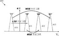
도 2에 도시된 예시적인 실시예에서, 각각의 저장 소자(storage element)는 각각의 메모리 셀 내에 2개의 비트의 데이터를 저장하기 위해 4개의 가능한 데이터 상태를 이용한다. 도 2는 각각의 피크가 하나의 상태에 대응하는 4개의 피크(210 내지 213)를 도시한다. 다중 레벨 셀 플래시 디바이스에서, 임계 전압 분포 그래프(200)의 상이한 피크(210 내지 213)는 셀 내에 2개의 비트를 저장하기 위해 사용된다.In the exemplary embodiment shown in FIG. 2, each storage element utilizes four possible data states to store two bits of data in each memory cell. Figure 2 shows four peaks 210-213 where each peak corresponds to one state. In multi-level cell flash devices, the different peaks 210-213 of the threshold
임계 전압 분포 그래프(200)의 피크(210 내지 213)는 대응하는 2진값으로 라벨링되어 있다. 따라서, 셀이 제 1 상태(210)에 있을 때, 이는 하위 비트[또한 최하위 비트(LSB)라 알려짐]에 대해 "1"을 상위 비트[또한 최상위 비트(MSB)라 알려짐]에 대해 "1"을 표현한다. 상태(210)는 일반적으로 셀의 초기의 비프로그래밍된 또는 소거된 상태이다. 마찬가지로, 셀이 제 2 상태(211)에 있을 때, 이는 하위 비트에 대해 "0"을, 상위 비트에 대해 "1"을 표현한다. 셀이 제 3 상태(212)에 있을 때, 이는 하위 비트에 대해 "0"을, 상위 비트에 대해 "0"을 표현한다. 마지막으로, 셀이 제 4 상태(213)에 있을 때, 이는 하위 비트에 대해 "1"을, 상위 비트에 대해 "0"을 표현한다.
임계 전압 분포(210)는 0 볼트 미만의 네거티브 임계 전압 레벨을 갖는 소거된 상태("11" 데이터 상태)에 있는 어레이 내의 셀의 임계 전압(Vt)의 분포를 표현한다. "10" 및 "00" 사용자 데이터를 각각 저장하는 메모리 셀의 임계 전압 분포(211, 212)는 각각 0 내지 1 볼트와 1 내지 2 볼트에 있는 것으로 도시되어 있다. 임계 전압 분포(213)는 판독 대역 전압의 2 내지 4.5 볼트 사이의 임계 전압 레벨 세트를 갖고 "01" 데이터로 프로그래밍되어 있는 셀의 분포를 나타낸다.The
따라서, 도 2의 예시적인 실시예에서, 0 볼트, 1 볼트 및 2 볼트는 각각의 레벨 또는 상태 사이의 전압 레벨 임계치로서 사용될 수 있다. 전압 레벨 임계치는 소정의 셀의 상태 또는 전압 레벨을 결정하기 위해 플래시 메모리(160)[예를 들어, 플래시 메모리(160) 내의 감지 회로]에 의해 사용된다. 플래시 메모리(160)는 전압 레벨 임계치에 대한 측정된 전압의 비교에 기초하여 각각의 셀에 하나 이상의 비트를 할당할 수 있고, 이들 비트는 이어서 플래시 제어 시스템(110)에 경판정으로서 전송된다. 추가로 또는 대안적으로, 소프트 정보를 사용하는 구현예에서, 플래시 메모리(160)는 측정된 전압 또는 측정된 전압의 정량화된 버전을 소프트 정보로서 플래시 제어 시스템(110)에 전송할 수 있고, 여기서 메모리 셀 내에 저장된 비트의 수보다 많은 수의 비트가 측정된 전압을 표현하는데 사용된다.Thus, in the exemplary embodiment of FIG. 2, zero volts, one volt, and two volts can be used as the voltage level threshold between each level or state. The voltage level threshold is used by the flash memory 160 (e.g., the sense circuit in the flash memory 160) to determine the state or voltage level of a given cell. The
셀은 통상적으로 잘 알려진 프로그램/검증 기술을 사용하여 프로그래밍된다. 일반적으로, 프로그램/검증 사이클 중에, 플래시 메모리(160)는 최소 타겟 임계 전압이 초과될 때까지 셀 트랜지스터 내에 전하를 저장하기 위해 증가하는 전압을 점진적으로 인가한다. 예를 들어, 도 2의 예에서 '10' 데이터 상태를 프로그래밍할 때, 플래시 메모리(160)는 0.4 V의 최소 타겟 임계 전압이 초과될 때까지 셀 트랜지스터 내에 전하를 저장하기 위해 증가하는 전압을 점진적으로 인가할 수 있다.The cells are typically programmed using well known program / verification techniques. Generally, during a program / verify cycle, the
이하에 더 설명되는 바와 같이, 단일의 메모리 셀 내에 저장된 2개의 비트의 각각은 상이한 페이지로부터 온다. 달리 말하면, 각각의 메모리 셀 내에 저장된 2개의 비트의 각각의 비트는 상이한 페이지 어드레스를 전달한다. 도 2에 도시된 우측 비트는 하위 페이지 어드레스가 입력될 때 액세스된다. 좌측 비트는 상위 페이지 어드레스가 입력될 때 액세스된다.As will be described further below, each of the two bits stored in a single memory cell comes from a different page. In other words, each bit of the two bits stored in each memory cell carries a different page address. The right bit shown in Fig. 2 is accessed when a lower page address is input. The left bit is accessed when the upper page address is input.
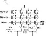
도 3은 다중 레벨 셀(MLC) 플래시 메모리 디바이스(160) 내의 예시적인 플래시 셀 어레이(300)의 아키텍쳐를 도시하고, 여기서 각각의 예시적인 셀은 통상적으로 2개의 비트를 저장하는 부유 게이트 트랜지스터에 대응한다. 도 3에서, 각각의 셀은 2개의 비트가 속하는 2개의 페이지에 대한 2개의 수와 관련된다. 예시적인 셀 어레이 섹션(300)은 워드라인 n 내지 n+2 및 4개의 비트라인을 나타낸다. 예시적인 플래시 셀 어레이(300)는 짝수 및 홀수 페이지로 분할되고, 여기서 예를 들어 짝수(숫자 0 및 2를 갖는 셀과 같은)를 갖는 셀은 짝수 페이지에 대응하고, 홀수(숫자 1 및 3을 갖는 셀과 같은)를 갖는 셀은 홀수 페이지에 대응한다. 워드라인 n은 예를 들어 짝수 비트라인 내에 짝수 페이지 0 및 2를 저장하고, 홀수 비트라인 내에 홀수 페이지 1 및 3을 저장한다.3 illustrates the architecture of an exemplary
게다가, 도 3은 짝수 또는 홀수 비트라인 셀이 선택되어 지시된 순서로 순차적으로(상향식) 프로그래밍되는 예시적인 프로그램 시퀀스를 지시한다. 숫자는 페이지가 프로그래밍되는 순서를 지시한다. 예를 들어, 페이지 0은 페이지 1 이전에 프로그램된다. 짝수 및 홀수 페이지의 프로그래밍의 추가의 설명을 위해, 예를 들어, 본 명세서에 참조로서 포함되어 있는 박기태(K. T. Park) 등의 "MLC NAND 플래시 메모리에 대한 일시적인 LSB 저장 및 병렬 MSB 프로그램 체계를 갖는 제로화 셀간 간섭 페이지 아키텍쳐", IEEE Journal of Solid State Circuits, Vol. 43, No. 4, 919-928(2008년 4월)을 참조하라.In addition, Figure 3 shows an exemplary program sequence in which even or odd bit line cells are selected and programmed sequentially (bottom-up) in the indicated order. The numbers indicate the order in which the pages are programmed. For example,
도 4는 도 2의 전압 할당 체계에 대한 예시적인 2단 MLC 프로그래밍 체계(400)를 도시한다. 도 4에 도시된 바와 같이, LSB 프로그램 단계 중에, 소거된 상태(410)에 있는 선택된 셀의 상태는 LSB가 0이면 최하위 프로그래밍된 상태(411)로 이동한다. 따라서, LSB 프로그래밍 단계에서, 메모리 셀은 소거된 상태 '11'로부터 '10'으로 프로그래밍된다. 다음, MSB 프로그램 단계 중에, 상태 '00'(412) 및 상태 '01'(413)은 이전의 LSB 데이터에 따라 순차적으로 형성된다. 일반적으로, MSB 프로그래밍 단계 중에, '10' 상태는 '00'으로 프로그래밍되고, 상태 '11'은 '01'로 프로그래밍된다.FIG. 4 illustrates an exemplary two-stage
도 4의 프로그래밍 체계(400)는 상태(410)로부터 상태(413)로의 상태의 변화와 관련된 최대 전압 시프트를 도시한다는 것이 주목된다. 다수의 프로그래밍 체계가 상태의 변화와 관련된 최대 전압 시프트를 감소시키고, 이에 의해 전압 시프트에 의해 발생된 ICI를 감소시키기 위해 제안되거나 제의되어 왔다.It is noted that the
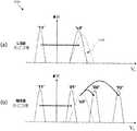
도 5(a) 및 도 5(b)는 집합적으로 이웃하는 셀 상에 부과된 ICI를 감소시키는 대안적인 MLC 프로그래밍 체계(500)를 도시한다. 도 5(a)에 도시된 바와 같이, LSB 프로그래밍 단계 중에, 메모리 셀은 SLC 프로그래밍과 유사한 방식으로 상태 '11'로부터 일시적인(또는 중간) 상태로서 상태 'x0'으로 프로그래밍된다. 동일한 워드라인 내의 이웃 셀이 또한 LSB 프로그래밍된 후에, ICI에 기인하여 도 5(a)의 피크(510)에 의해 도시된 바와 같이 분배가 가능하게는 확장된다. 그 후에, 도 5(b)에 도시된 MSB 프로그래밍 스테이지에서, 'x0' 상태는 입력 데이터 또는 다른 것에 대응하는 최종 데이터로서 '00' 및 '10'으로 프로그래밍되고, '11' 상태는 최종 '01' 상태로 프로그래밍된다. 일반적으로, '11' 셀을 제외한 모든 메모리 셀은 이웃하는 셀에 의해 발생되는 ICI가 상당히 감소될 수 있도록 LSB 데이터에 대한 일시적인 프로그래밍된 상태로부터 MSB 프로그래밍 상태에서 그 최종 상태로 재프로그래밍된다. 최종 상태의 셀은 최종 상태로 재프로그래밍되어 있기 때문에, 중간 상태에 있는 동안 경험되는 ICI를 겪지 않게 될 수 있다. 최종 상태의 셀은 단지 최종 상태에 있은 후에 경험된 ICI만을 겪게 될 수 있다. 전술된 바와 같이, 도 5(a) 및 도 5(b)의 다단계 프로그래밍 시퀀스는, 중간 프로그램 상태를 사용하여, 최대 전압 변화 및 따라서 이들 전압 변화에 의해 발생된 ICI를 감소시킨다. 예를 들어 MSB 프로그래밍 단계 중의 최대 전압 시프트는 각각 상태 '11'로부터 '01'로, 그리고 상태 'x0'으로부터 '10'으로의 전이와 관련된다는 것을 도 5에서 알 수 있다. 이들 전압 시프트는 도 4의 상태 '11'로부터 '01'로의 최대 전압 시프트보다 상당히 작다.Figures 5 (a) and 5 (b) collectively show an alternative
도 6은 다중 레벨 셀(MLC) 플래시 메모리 디바이스(130) 내의 예시적인 플래시 셀 어레이(600)를 더 상세히 도시한다. 도 6에 도시된 바와 같이, 플래시 셀 어레이(600)는 플래시 셀(ci)당 3개의 비트를 저장한다. 도 6은 하나의 블록에 대한 플래시 셀 어레이 아키텍쳐를 도시하고, 여기서 각각의 예시적인 셀은 통상적으로 3개의 비트를 저장하는 부유 게이트 트랜지스터에 대응한다. 예시적인 셀 어레이(600)는 m개의 워드라인 및 n개의 비트라인으로 이루어진다. 통상적으로, 현재의 다중 페이지 셀 플래시 메모리에서, 단일 셀 내의 비트는 상이한 페이지에 속한다. 도 6의 예에서, 각각의 셀에 대한 3개의 비트가 3개의 상이한 페이지에 대응하고, 각각의 워드라인은 3개의 페이지를 저장한다. 이하의 설명에서, 페이지 0, 1 및 2는 워드라인 내의 하위, 중간 및 상위 페이지 레벨이라 칭한다.6 shows an exemplary
전술된 바와 같이, 플래시 셀 어레이는 짝수 및 홀수 페이지로 더 분할될 수 있고, 여기서 예를 들어 짝수를 갖는 셀(도 6의 셀 2 및 4와 같은)은 짝수 페이지에 대응하고 홀수를 갖는 셀(도 6의 셀 1 및 3과 같은)은 홀수 페이지에 대응한다. 이 경우에, 페이지(페이지 0과 같은)는 짝수 셀 내의 짝수 페이지(짝수 페이지 0) 및 홀수 셀 내의 홀수 페이지(홀수 페이지 0)를 포함할 수 있다.As described above, the flash cell array can be further divided into even and odd pages, where for example a cell with an even number (such as
셀간 간섭Intercell interference
전술된 바와 같이, ICI는 셀들 사이의 기생 캐패시턴스의 결과이고, 일반적으로 가장 현저한 왜곡의 소스 중 하나로 고려된다. 도 7은 다수의 예시적인 공격자 셀(720)로부터의 기생 캐패시턴스에 기인하여 타겟 셀(710)에 대해 존재하는 ICI를 도시한다. 이하의 표기가 도 7에 이용되고 있다.As described above, ICI is the result of parasitic capacitance between cells and is generally considered to be one of the most significant sources of distortion. FIG. 7 shows the ICI present for the
WL: 워드라인,WL: word line,
BL: 비트라인,BL: bit line,
BLo: 홀수 비트라인BLo: odd bit line
BLe: 짝수 비트라인, 및BLe: an even bit line, and
C: 캐패시턴스.C: capacitance.
본 발명은 타겟 셀(710)이 프로그래밍된 후에 프로그래밍되는 공격자 셀(720)에 의해 ICI가 발생되는 것을 인식한다. ICI는 타겟 셀(710)의 전압(Vt)을 변경한다. 예시적인 실시예에서, "상향식" 프로그래밍 체계가 취해지고 워드라인 i 및 i+1 내의 인접 공격자 셀이 타겟 셀(710)에 대한 ICI를 발생시킨다. 블록의 이러한 상향식 프로그래밍에 의해, 하위 워드라인 i-1로부터의 ICI가 제거되고, 최대 5개의 이웃하는 셀이 도 7에 도시된 바와 같이 공격자 셀(720)로서 ICI에 기여한다. 그러나, 본 명세서에 개시된 기술은 당 기술 분야의 숙련자에 명백할 수 있는 바와 같이, 워드라인 i-1과 같은 다른 워드라인으로부터의 공격자 셀이 마찬가지로 ICI에 기여하는 경우에 보편화될 수 있다는 것이 주목된다. 워드라인 i-1, i 및 i+1로부터의 공격자 셀이 ICI에 기여하면, 최대 8개의 가장 근접한 이웃하는 셀이 고려될 필요가 있다. 타겟 셀로부터 멀리 이격된 다른 셀은 ICI에 대한 이들의 기여가 무시할 만하면, 무시될 수 있다. 일반적으로, 공격자 셀(720)은 소정의 타겟 셀(710) 이후에 프로그래밍되는 공격자 셀(720)을 식별하기 위해 프로그래밍 시퀀스 체계(상향식 또는 짝수/홀수 기술과 같은)를 분석함으로써 식별된다.The present invention recognizes that ICI is generated by the
타겟 셀(710) 상에 공격자 셀(720)에 의해 발생된 ICI는 예시적인 실시예에서 이하와 같이 모델링될 수 있는데,The ICI generated by the

여기서,

일반적으로, Vt는 셀 상에 저장되고 판독 작업 중에 얻어진 데이터를 표현하는 전압이다. Vt는 예를 들어 셀당 저장된 비트의 수보다 높은 정밀도를 갖는 소프트 전압값, 또는 셀당 저장된 비트의 수(예를 들어 3 비트/셀 플래시에 대해 3 비트)와 동일한 분해능을 갖는 하드 전압 레벨로 정량화된 값일 수 있다.Generally, Vt is the voltage stored on the cell and representing the data obtained during the read operation. Vt may be quantified as a soft voltage value with a precision that is higher than the number of bits stored per cell, or a hard voltage level with the same resolution as the number of bits stored per cell (e.g., 3 bits for 3 bits / cell flash) Lt; / RTI >
시스템 레벨 고려Consider system level
도 8은 본 발명에 따른 제어기 기반 ICI 완화 기술을 통합하는 예시적인 플래시 메모리 시스템(800)의 개략 블록 다이어그램이다. 도 8에 도시된 바와 같이, 예시적인 플래시 메모리 시스템(800)은 인터페이스(850)에 의해 접속된 플래시 제어 시스템(810) 및 플래시 메모리 블록(860)을 포함한다. 예시적인 플래시 제어 시스템(810)은 통상적으로 하나 이상의 집적 회로 상에 플래시 제어기(820) 및 판독 채널(825)을 포함한다. 예시적인 플래시 제어기(820)는 예를 들어 본 발명의 특징 및 기능을 지원하기 위해 본 명세서에서 수정된 바와 같이, 잘 알려진 상업적으로 입수 가능한 기술 및/또는 제품을 사용하여 구현될 수 있다.FIG. 8 is a schematic block diagram of an exemplary
예시적인 판독 채널(825)은 신호 프로세싱 유닛(830), 인코더/디코더 블록(840) 및 하나 이상의 버퍼(845)를 포함한다. 용어 "판독 채널"은 마찬가지로 기록 채널을 포함할 수 있다. 대안 실시예에서, 인코더/디코더 블록(840) 및 몇몇 버퍼(845)는 플래시 제어기(820) 내부에 구현될 수 있다. 인코더/디코더 블록(840) 및 버퍼(845)는 예를 들어 본 발명의 특징 및 기능을 제공하기 위해 본 명세서에서 수정되는 바와 같이 잘 알려진 상업적으로 입수 가능한 기술 및/또는 제품을 사용하여 구현될 수 있다.The
예시적인 신호 프로세싱 유닛(830)은 예를 들어 도 10 내지 도 12와 관련하여 이하에 더 설명되는 하나 이상의 ICI 완화 프로세스(835)를 구현하는 하나 이상의 프로세서를 포함한다. 게다가, 도 8에 도시된 다양한 블록 사이의 데이터 흐름은 또한 예를 들어 도 10 내지 도 12와 관련하여 이하에 더 설명된다. 일반적으로, 도 11 및 도 12와 관련하여 이하에 더 설명되는 바와 같이, 판독 작업 중에 ICI 완화를 수행하기 위해, 하나 이상의 ICI 완화 프로세스(835)는 하드 또는 소프트 판독값에 기초하여 새로운 판독값을 컴퓨팅한다. 마찬가지로, 도 10과 관련하여 이하에 더 설명되는 바와 같이, 기록 작업 중에 ICI 완화를 수행하기 위해, 하나 이상의 ICI 완화 프로세스(835)는 타겟 및 공격자 셀에 대한 프로그램 데이터에 기초하여 메모리 어레이(870) 내에 저장될 사전 보상된 프로그램 값을 생성한다.Exemplary
예시적인 플래시 메모리 블록(860)은 잘 알려진 상업적으로 입수 가능한 기술 및/또는 제품을 사용하여 각각 구현될 수 있는 메모리 어레이(870) 및 하나 이상의 버퍼(880)를 포함한다.Exemplary
도 10 및 도 11과 관련하여 이하에 더 설명되는 본 발명의 일 양태에 따르면, 예시적인 인터페이스(850)는 공격자 셀과 관련된 정보를 표현하는 값과 같은 통상의 플래시 메모리 시스템에 대한 추가의 정보를 전달할 필요가 있을 수 있다. 따라서, 인터페이스(850)는 통상의 플래시 메모리 시스템의 인터페이스보다 높은 용량(예를 들어, 더 많은 입력 또는 출력 핀) 또는 빠른 레이트를 가질 필요가 있을 수 있다.According to one aspect of the invention described further below in connection with Figures 10 and 11, the
기록 작업 중에, 인터페이스(850)는 통상적으로 페이지 또는 워드라인 레벨 액세스 기술을 사용하여 타겟 셀 내에 저장될 사전 보상된 프로그램 값을 전달한다. 예시적인 페이지 또는 워드라인 레벨 액세스 기술의 더 상세한 설명을 위해, 예를 들어 본 명세서에 참조로서 포함되어 있는 2009년 3월 11일 출원된 발명의 명칭이 "페이지간 섹터, 다중 페이지 코딩 및 페이지당 코딩을 갖는 다중 레벨 셀 플래시 메모리 디바이스 내에 데이터를 저장하기 위한 방법 및 장치"인 국제 특허 출원 제 PCT/US09/36810호를 참조하라. 통상적으로, 사전 보상된 프로그램 값의 수는 통상적으로 원래 프로그램 값의 수보다 크기 때문에, 원래 프로그램 값을 표현하기 위한 것보다 많은 비트가 사전 보상된 프로그램 값을 표현하기 위해 요구된다. 따라서, 기록측 ICI 완화를 위해, 인터페이스(850)는 통상의 인터페이스보다 많은 데이터를 전달할 필요가 있다.During a write operation, the
판독 작업 중에, 인터페이스(850)는 타겟 및 공격자 셀에 대해 메모리 어레이(870)로부터 얻어지고 있는 하드 및/또는 소프트 판독값을 전달한다. 예를 들어, 타겟 셀을 갖는 페이지에 대한 판독값에 추가하여, 상위/하위 워드라인 또는 이웃하는 짝수 또는 홀수 비트라인 내의 하나 이상의 인접 페이지에 대한 판독값은 인터페이스 버스를 통해 전달된다.During a read operation, the
도 8의 실시예에서, 개시된 기록측 또는 판독측 ICI 완화 기술은 통상적으로 최하위 영역을 성취하기 위해 논리 회로에 대해 최적화된 프로세스 기술에서 플래시 메모리 외부에서 구현된다. 그러나, 이는 인터페이스(850) 상에 전달되어야 하는 추가의 공격자 셀 데이터의 희생이다.In the embodiment of FIG. 8, the disclosed write-side or read-side ICI mitigation techniques are typically implemented outside the flash memory in a process technology that is optimized for logic circuits to achieve the lowermost region. However, this is a sacrifice of additional attacker cell data that must be delivered on
도 9는 본 발명의 대안 실시예에 따른 메모리 기반 ICI 완화 기술을 통합하는 예시적인 플래시 메모리 시스템(900)의 개략 블록 다이어그램이다. 도 9에 도시된 바와 같이, 예시적인 플래시 메모리 시스템(900)은 인터페이스(950)에 의해 접속된 플래시 제어 시스템(910) 및 플래시 메모리 블록(960)을 포함한다. 예시적인 플래시 제어 시스템(910)은 통상적으로 하나 이상의 집적 회로 상에 플래시 제어기(920) 및 선택적 판독 채널(925)을 포함한다. 예시적인 판독 채널(925)은 인코더/디코더 블록(940) 및 하나 이상의 버퍼(945)를 포함한다. 대안 실시예에서, 인코더/디코더 블록(940) 및 몇몇 버퍼(945)는 플래시 제어기(920) 내부에 구현될 수 있다. 예시적인 플래시 제어기(920)는 예를 들어 본 발명의 특징 및 기능을 지원하기 위해 본 명세서에서 수정된 바와 같은 잘 알려진 상업적으로 입수 가능한 기술 및/또는 제품을 사용하여 구현될 수 있다. 인코더/디코더 블록(940) 및 버퍼(945)는 잘 알려진 상업적으로 입수 가능한 기술 및/또는 제품을 사용하여 구현될 수 있다.9 is a schematic block diagram of an exemplary
예시적인 플래시 메모리 블록(960)은 잘 알려진 상업적으로 입수 가능한 기술 및/또는 제품을 사용하여 각각 구현될 수 있는 메모리 어레이(970) 및 하나 이상의 버퍼(980)를 포함한다. 게다가, 예시적인 플래시 메모리 블록(960)은 하나 이상의 ICI 완화 프로세스(990)를 구현하는 하나 이상의 프로세서를 포함하는 예시적인 신호 프로세싱 유닛(985)을 포함한다. 일반적으로, 판독 작업 중에 ICI 완화를 수행하기 위해, 하나 이상의 ICI 완화 프로세스(990)가 메모리 어레이(970)로부터 판독된 하드 또는 소프트 판독값에 기초하여 새로운 판독값을 컴퓨팅한다. 마찬가지로, 기록 작업 중에 ICI 완화를 수행하기 위해, 하나 이상의 ICI 완화 프로세스(990)는 타겟 및 공격자 셀에 대해 플래시 제어기(910)로부터 검색된 프로그램 데이터에 기초하여 사전 보상된 프로그램 값을 생성한다.The exemplary
도 10 및 도 11과 관련하여 이하에 더 설명되는 본 발명의 일 양태에 따르면, 예시적인 인터페이스(950)는 공격자 셀과 관련된 정보를 표현하는 값과 같은 통상의 플래시 메모리 시스템에 대한 추가의 정보를 전달할 필요가 있을 수 있다. 따라서, 인터페이스(950)는 통상의 플래시 메모리 시스템의 인터페이스보다 높은 용량(예를 들어, 더 많은 입력 또는 출력 핀) 또는 빠른 레이트를 가질 필요가 있다.According to one aspect of the invention described further below in connection with Figures 10 and 11, the
기록 작업 중에, 인터페이스(950)는 타겟 및 공격자 셀 내에 저장될 프로그램 데이터를 전달하고, 사전 보상된 프로그램 값이 플래시 메모리(960) 내부에서 컴퓨팅된다. 인터페이스(950)는 예를 들어 통상의 플래시 메모리 시스템에서와 같이 타겟 셀을 갖는 페이지에 대해 프로그램 데이터를, 게다가 공격자 셀을 갖는 인접 워드라인 또는 짝수 또는 홀수 비트 라인에 대해 프로그램 데이터를 전달할 수 있다. 통상적으로, 사전 보상된 프로그램 값을 표현하기 위한 것보다 적은 비트가 이 프로그램 데이터를 표현하는데 요구된다. 따라서, 기록측 ICI 완화에 대해, 인터페이스(950)는 통상적으로 인터페이스(850)보다 적은 대역폭을 필요로 할 수 있다. 그러나, 이는 통상적으로 논리 회로가 아니라 메모리에 대해 최적화되는 플래시 메모리를 제조하는데 사용된 메모리 프로세스 기술을 사용하여 메모리 내부에서 기록측 ICI 완화 프로세스를 구현하는 것을 희생한다.During the write operation, the
판독 작업 중에, 인터페이스(950)는 타겟 셀(들) 및 선택적으로 공격자 셀에 대해 ICI 완화 프로세스(990)에 의해 컴퓨팅되었던 새로운 하드 또는 소프트 판독값 또는 데이터를 전달한다. 통상적으로, 단일 판독 액세스에 대해 전달된 정보는 데이터의 페이지 또는 워드라인이다. 통상적으로 논리 회로가 아니라 메모리에 대해 최적화된 플래시 메모리를 제조하는데 사용된 메모리 프로세스 기술을 사용하여 메모리 내부에 판독측 ICI 완화 프로세스를 구현하는 것을 희생시켜, 타겟 셀에 대한 송신 데이터만이 인터페이스(950)의 대역폭 요건을 감소시킨다는 것이 주목된다.During the read operation, the
도 8 및 도 9의 ICI 완화 기술의 다양한 실시예에서 이용된 용량성 커플링 계수(kx, ky 및 kxy)는 플래시 제어 시스템(810, 910) 및/또는 플래시 메모리 블록(860, 960)에서 컴퓨팅될 수 있다는 것이 주목된다. 용량성 커플링 계수(kx, ky 및 kxy)가 각각의 인터페이스(850, 950)에 전달될 필요가 있을 수 있다. 용량성 커플링 계수는 적응성일 수 있고, 연속적인 임시의 또는 주기적인 기초로 업데이트될 수 있다는 것이 주목된다.The capacitive coupling coefficients (kx , ky and kxy ) used in the various embodiments of the ICI mitigation techniques of Figures 8 and 9 are determined by the
예시적인 ICI 완화 프로세스(835, 990)의 더 상세한 설명을 위해, 예를 들어 본 출원과 동일자로 각각 출원되어 본 명세서에 참조로서 포함되어 있는 발명의 명칭이 "플래시 메모리 내의 기록측 셀간 간섭 완화 방법 및 장치(Methods and Apparatus for Write-Side Intercell Interference Mitigation in Flash Memories)"인 PCT 특허 출원 제호 및 발명의 명칭이 "플래시 메모리 내의 판독측 셀간 간섭 완화 방법 및 장치(Methods and Apparatus for Read-Side Intercell Interference Mitigation in Flash Memories)"인 PCT 특허 출원 제호를 참조하라.For a more detailed description of exemplary ICI mitigation processes 835 and 990, for example, the name of the invention, each of which is assigned to the same assignee as the present application and is incorporated herein by reference, &Quot; PCT Patent Application ", which is a " Method and Apparatus for Write-Side Intercell Interference Mitigation in Flash Memories & PCT patent application entitled " Method and Apparatus for Read-Side Intercell Interference Mitigation in Flash Memories " See the issue.
개량된 인터페이스(850, 950)The
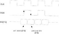
전술된 바와 같이, 본 발명은 플래시 메모리 제어기(820, 920)와 플래시 메모리 어레이(870, 970) 사이에 개량된 인터페이스(850, 950)를 제공한다. 본 발명의 일 양태에 따르면, 타겟 셀(710)에 대한 데이터는 클럭 신호의 제 1 에지(상승 에지와 같은) 상에 전달되고, 전달된 데이터에 대한 추가의 정보가 클럭 신호의 제 2 에지(하강 에지와 같은) 상에 전송된다. 개시된 인터페이스는 상당히 증가하는 전력 소산 또는 표면적 없이 전송된 데이터에 대한 추가의 정보를 위한 추가의 대역폭을 제공한다.As described above, the present invention provides an
일반적으로, 인터페이스(850, 950)는 예를 들어 본 발명의 특징 및 기능을 제공하도록 본 명세서에서 수정된 바와 같이, 본 명세서에 참조로서 포함되어 있는 ONFI 2.0 표준에 따라 구현될 수 있다. 이 방식으로 동일한 인터페이스(850, 950)가 소프트 데이터를 프로세싱하고 추가의 기록 데이터를 송신하는 능력 없이 레가시 플래시 제어기(820, 920)에 대해 사용될 수 있다. 레가시 플래시 제어기(820, 920)는 본 발명에 따라 하강 에지에 전송되는 추가의 데이터를 무시할 수 있다.In general, interfaces 850 and 950 may be implemented in accordance with the ONFI 2.0 standard, which is incorporated herein by reference, for example, as modified herein to provide features and functionality of the present invention. In this manner, the
전술된 바와 같이, ONFI 버전 2.0은 클럭 신호의 상승 및 하강 에지의 모두에 데이터를 전달하기 위해 더블 데이터 레이트(DDR) 기술을 사용한다. ONFI 버전 2.0은 NAND 플래시 인터페이스의 데이터 전달 용량을 증가시키지만, 성능을 개량할 수 있는 추가의 정보를 전달하기 위한 추가의 대역폭을 제공하지 않는다. 일 예시적인 실시예에서, 타겟 셀(710)을 위한 데이터는 클럭 신호의 제 1 에지(상승 에지와 같은) 상에 전달되고, 소프트 판독 데이터 및 인접 기록 데이터와 같은 전달된 데이터에 대한 추가의 정보는 클럭 신호의 제 2 에지(하강 에지와 같은) 상에 전달된다.As described above, ONFI version 2.0 uses a double data rate (DDR) technique to transfer data to both the rising and falling edges of the clock signal. ONFI version 2.0 increases the data transfer capacity of a NAND flash interface, but does not provide additional bandwidth to carry additional information to improve performance. In one exemplary embodiment, the data for the
A. 기록 액세스A. Historical Access
도 10은 본 발명에 따른 기록 액세스를 위한 관련 파형을 도시한다. 도 10에 도시된 바와 같이, 플래시 메모리의 DQ 버스 상의 데이터는 CLK 신호 또는 DQS(스트로브) 신호 또는 양자 모두를 사용하여 통상적으로 클럭킹된다. 일반적으로, DQS 신호가 가능화될 때, DQS 신호는 CLK 신호의 각각의 상승 에지 및 하강 에지에 각각 대응하는 상승 에지 및 하강 에지를 갖는다.Figure 10 shows a related waveform for a write access in accordance with the present invention. As shown in FIG. 10, data on the DQ bus of the flash memory is typically clocked using a CLK signal or a DQS (strobe) signal or both. In general, when the DQS signal is enabled, the DQS signal has a rising edge and a falling edge corresponding to the respective rising and falling edges of the CLK signal, respectively.
ONFI 버전 2.0은 클럭 신호의 상승 및 하강 에지의 모두에 데이터를 전달한다. 본 발명은 CLK 신호의 제 1 에지(상승 에지와 같은) 상의 타겟 셀(710)에 대한 데이터를 전달하고, 타겟 셀(710)에 대한 전달된 데이터에 대한 추가의 정보는 CLK 신호의 제 2 에지(하강 에지와 같은) 상에 전달된다. 기록 액세스에서, 하강 에지 상의 증가된 대역폭은 플래시 메모리 제어기(820, 920)로부터 플래시 메모리 어레이(870, 970)로 각각 추가의 정보(공격자 데이터 정보와 같은)를 전달하는데 사용될 수 있다. 일 예시적인 용례에서, 개량된 인터페이스(850, 950)는 ICI 완화를 위한 타겟 셀(710)의 공격자 셀(720)에 대한 정보의 전달을 가능하게 하는 추가의 대역폭을 제공한다. 예를 들어, CLK(또는 DQS) 신호의 하강 에지 상에 래칫된 데이터는 타겟 셀(710)에 대한 상위 인접 비트를 전달할 수 있고, 이는 셀간 간섭을 완화하기 위해 프로그래밍된 전압을 조정하도록 ICI 완화 프로세스(835, 990)에 의해 사용될 수 있다.ONFI version 2.0 transfers data to both the rising and falling edges of the clock signal. The invention conveys data for the
B. 판독 액세스B. Read Access
도 11은 본 발명에 따른 판독 액세스를 위한 관련 파형을 도시한다. 도 11에 도시된 바와 같이, 플래시 메모리의 DQ 버스 상의 데이터는 CLK 신호 또는 DQS(스트로브) 신호 또는 양자 모두를 사용하여 통상적으로 클럭킹된다. 일반적으로, DQS 신호가 가능화될 때, DQS 신호는 CLK 신호의 각각의 상승 에지 및 하강 에지에 각각 대응하는 상승 에지 및 하강 에지를 갖는다.11 shows a related waveform for a read access in accordance with the present invention. As shown in FIG. 11, data on the DQ bus of the flash memory is typically clocked using a CLK signal or a DQS (strobe) signal or both. In general, when the DQS signal is enabled, the DQS signal has a rising edge and a falling edge corresponding to the respective rising and falling edges of the CLK signal, respectively.
ONFI 버전 2.0은 클럭 신호의 상승 및 하강 에지의 모두에 데이터를 전달한다. 본 발명은 CLK 신호의 제 1 에지(상승 에지와 같은) 상의 타겟 셀(710)에 대한 데이터를 전달하고, 타겟 셀(710)에 대한 전달된 데이터에 대한 추가의 정보는 CLK 신호의 제 2 에지(하강 에지와 같은) 상에 전달된다. 판독 액세스에서, 하강 에지 상의 증가된 대역폭은 상승 에지 상에 전달되었던 타겟 셀(710)에 대한 하드 데이터와 관련된 타겟 셀(710)에 대한 소프트 데이터(예를 들어, 확률 정보)를 전달하는데 사용될 수 있다. 전달은 플래시 메모리 어레이(870, 970)로부터 플래시 메모리 제어기(820, 920)로 각각 이루어진다. 일 예시적인 용례에서, 개량된 인터페이스(850, 950)는 ICI 완화를 위한 타겟 셀(710)의 소프트 정보의 전달을 가능하게 하는 추가의 대역폭을 제공한다. 예를 들어, CLK(또는 DQS) 신호의 하강 에지 상에 래칫된 데이터는 타겟 셀(710)에 대한 소프트 데이터를 전달할 수 있고, 이는 개량된 에러 보정 및 셀간 간섭 완화를 위해 ICI 완화 프로세스(835, 990)에 의해 사용될 수 있다.ONFI version 2.0 transfers data to both the rising and falling edges of the clock signal. The invention conveys data for the
프로세스, 시스템 및 제조 물품 상세Process, system, and article of manufacture
본 명세서의 다수의 흐름도는 예시적인 단계의 순서를 설명하지만, 순서가 변경될 수 있는 것도 또한 본 발명의 실시예이다. 알고리즘의 다양한 치환은 본 발명의 대안 실시예로서 구현된다. 본 발명의 예시적인 실시예는 소프트웨어 프로그램 내의 프로세싱 단계에 대해 설명되었지만, 다양한 기능이 소프트웨어 프로그램 내의, 회로 소자 또는 상태 머신에 의해 하드웨어 내의, 또는 소프트웨어 및 하드웨어의 모두의 조합 내의 프로세싱 단계로서 디지털 도메인에서 구현될 수 있다. 이러한 소프트웨어는 예를 들어 디지털 신호 프로세서, 응용 특정 집적 회로, 마이크로 제어기 또는 범용 컴퓨터에서 구체화될 수 있다. 이러한 하드웨어 및 소프트웨어는 집적 회로 내에 구현된 회로 내에서 구체화될 수 있다.It is also an embodiment of the present invention that many of the flowcharts herein illustrate the sequence of exemplary steps, although the order may change. Various permutations of the algorithm are implemented as an alternative embodiment of the present invention. While the exemplary embodiments of the present invention have been described with respect to the processing steps in a software program, it is to be understood that the various functions may be embodied in a software program, as a processing step in hardware by a circuit element or state machine, Can be implemented. Such software may be embodied in, for example, a digital signal processor, an application specific integrated circuit, a microcontroller, or a general purpose computer. Such hardware and software may be embodied in circuitry embodied within an integrated circuit.
따라서, 본 발명의 기능은 이들 방법을 실시하기 위한 방법 및 장치의 형태로 구체화될 수 있다. 본 발명의 하나 이상의 양태는 예를 들어 저장 매체 내에 저장되고, 머신 내에 로딩되고 그리고/또는 머신에 의해 실행되거나 몇몇 전송 매체를 통해 전송되건간에 프로그램 코드의 형태로 구체화될 수 있고, 여기서 프로그램 코드가 컴퓨터와 같은 머신 내에 로딩되어 실행될 때, 머신은 본 발명을 실시하기 위한 장치가 된다. 범용 프로세서 상에서 구현될 때, 프로그램 코드 세그먼트는 프로세서와 조합하여 특정 논리 회로와 유사하게 작동하는 디바이스를 제공한다. 본 발명은 또한 집적 회로, 디지털 신호 프로세서, 마이크로프로세서 및 마이크로 제어기 중 하나 이상으로 구현될 수 있다.Accordingly, the functions of the present invention may be embodied in the form of methods and apparatus for practicing those methods. One or more aspects of the present invention may be embodied in the form of program code, for example, whether stored in a storage medium, loaded into a machine and / or executed by a machine or transmitted via some transmission medium, When loaded and executed in a machine such as a computer, the machine becomes an apparatus for practicing the present invention. When implemented on a general-purpose processor, the program code segment provides a device that, in combination with the processor, operates similarly to a particular logic circuit. The invention may also be implemented with one or more of an integrated circuit, a digital signal processor, a microprocessor, and a microcontroller.
당 기술 분야에 공지된 바와 같이, 본 명세서에 설명된 방법 및 장치는 그에 구체화된 컴퓨터 판독 가능 코드 수단을 갖는 컴퓨터 판독 가능 매체를 자체로 포함하는 제조 물품으로서 분배될 수 있다. 컴퓨터 판독 가능 프로그램 코드 수단은 컴퓨터 시스템과 함께, 본 명세서에 설명된 방법을 수행하거나 장치를 생성하기 위한 단계의 전체 또는 일부를 수행하도록 작동 가능하다. 컴퓨터 판독 가능 매체는 판독 가능 매체[예를 들어, 플로피 디스크, 하드 드라이브, 컴팩트 디스크, 메모리 카드, 반도체 디바이스, 칩, 응용 특정 집적 회로(ASIC)]일 수 있고, 또는 전송 매체(예를 들어, 시간 분할 다중 접속, 코드 분할 다중 접속 또는 다른 무선 주파수 채널을 사용하는 광 파이버, 월드와이드 웹, 케이블 또는 무선 채널을 포함하는 네트워크)일 수 있다. 컴퓨터 시스템과 함께 사용을 위해 적합한 정보를 저장할 수 있는 것으로 공지되거나 개발된 임의의 매체가 사용될 수 있다. 컴퓨터 판독 가능 코드 수단은 자기 매체 상의 자기 편차 또는 컴팩트 디스크의 표면 상의 높이 편차와 같은 명령 및 데이터를 컴퓨터가 판독하는 것을 가능하게 하기 위한 임의의 메커니즘이다.As is known in the art, the methods and apparatus described herein can be distributed as an article of manufacture that itself includes a computer-readable medium having computer-readable code means embodied therein. The computer readable program code means is operable with the computer system to perform all or part of the steps for performing the method described herein or for creating a device. The computer readable medium can be a readable medium (e.g., a floppy disk, a hard drive, a compact disk, a memory card, a semiconductor device, a chip, an application specific integrated circuit (ASIC) An optical fiber using a time division multiple access, a code division multiple access or other radio frequency channel, a network including a world wide web, a cable or a wireless channel). Any medium known or developed that can store information suitable for use with a computer system may be used. The computer readable code means is any mechanism for enabling a computer to read instructions and data such as magnetic deviations on magnetic media or height deviations on the surface of a compact disk.
본 명세서에 설명된 컴퓨터 시스템 및 서버는 본 명세서에 개시된 방법, 단계 및 기능을 구현하기 위한 관련 프로세서를 구성할 수 있는 메모리를 각각 포함한다. 메모리는 분배형 또는 로컬형일 수 있고, 프로세서는 분배형 또는 단일형일 수 있다. 메모리는 전기, 자기 또는 광학 메모리, 또는 이들 또는 다른 유형의 저장 디바이스의 임의의 조합으로서 구현될 수 있다. 더욱이, 용어 "메모리"는 관련 프로세서에 의해 액세싱되는 어드레스 가능한 공간 내의 어드레스로부터 판독되거나 그에 기록될 수 있는 임의의 정보를 포함하는데 충분히 광범위하게 해석되어야 한다. 이 정의에서, 네트워크 상의 정보는 관련 프로세서가 네트워크로부터 정보를 검색할 수 있기 때문에 메모리 내에 여전히 있다.The computer systems and servers described herein each include a memory capable of configuring an associated processor to implement the methods, steps, and functions disclosed herein. The memory may be distributed or local type, and the processor may be distributed or single type. The memory may be implemented as an electrical, magnetic or optical memory, or any combination of these or other types of storage devices. Moreover, the term "memory" should be interpreted broadly enough to include any information that can be read from or written to an address in an addressable space accessed by the associated processor. In this definition, information on the network is still in memory because the associated processor can retrieve information from the network.
본 명세서에 도시되고 설명된 실시예 및 변형예는 단지 본 발명의 원리의 예시이며 다양한 수정이 본 발명의 사상 및 범주로부터 벗어나지 않고 당 기술 분야의 숙련자들에 의해 구현될 수 있다는 것이 이해되어야 한다.
It is to be understood that the embodiments and variations illustrated and described herein are merely illustrative of the principles of the invention and that various modifications may be practiced by those skilled in the art without departing from the spirit and scope of the invention.
100: 플래시 메모리 시스템110: 제어 시스템
120: 플래시 제어기140: 인코더/디코더 블록
145: 버퍼160: 플래시 메모리 블록
170: 메모리 어레이180: 버퍼
600: 플래시 셀 어레이710: 타겟 셀
720: 공격자 셀800: 플래시 메모리 시스템
810: 제어 시스템820: 플래시 제어기
825: 판독 채널830: 신호 프로세싱 유닛
840: 인코더/디코더 블록845: 버퍼
860: 메모리 블록870: 메모리 어레이
880: 버퍼900: 플래시 메모리 시스템
910: 플래시 제어 시스템920: 플래시 제어기
925: 판독 채널940: 인코더/디코더 블록
945: 버퍼960: 플래시 메모리 블록
970: 메모리 어레이985: 신호 프로세싱 유닛100: flash memory system 110: control system
120: flash controller 140: encoder / decoder block
145: buffer 160: flash memory block
170: memory array 180: buffer
600: flash cell array 710: target cell
720: Attacker cell 800: flash memory system
810: Control system 820: Flash controller
825: Read channel 830: Signal processing unit
840: Encoder / decoder block 845: Buffer
860: memory block 870: memory array
880: buffer 900: flash memory system
910: flash control system 920: flash controller
925: Read channel 940: Encoder / decoder block
945: buffer 960: flash memory block
970: memory array 985: signal processing unit
Claims (15)
Translated fromKorean클럭 신호의 제 1 에지를 사용하여 상기 플래시 메모리 어레이 내의 타겟 셀(710)에 대한 데이터를 전송하는 단계와,
상기 클럭 신호의 제 2 에지를 사용하여 상기 타겟 셀에 대한 추가의 정보를 전송하는 단계를 포함하되,
상기 클럭 신호의 각각의 에지의 타입은 하강 에지 타입(a falling edge type) 및 상승 에지 타입(a rising edge type) 중 하나이고, 상기 클럭 신호의 제 1 에지의 타입은 상기 클럭 신호의 제 2 에지의 타입과는 상이하고, 상기 데이터는 상기 추가의 정보와는 상이한 타입인
플래시 메모리 제어기와 플래시 메모리 어레이 사이의 인터페이싱 방법.
A method of interfacing between a flash memory controller (120) and a flash memory array (160)
Transmitting data for a target cell (710) in the flash memory array using a first edge of a clock signal;
And transmitting additional information for the target cell using a second edge of the clock signal,
Wherein the type of each edge of the clock signal is one of a falling edge type and a rising edge type and the type of the first edge of the clock signal is a second edge of the clock signal, And the data is of a type different from the type of the additional information
A method for interfacing between a flash memory controller and a flash memory array.
상기 전송하는 단계들은 기록 액세스를 포함하고, 상기 추가의 정보는 상기 타겟 셀과 연관된 하나 이상의 공격자 셀(720)에 대한 정보를 포함하는
플래시 메모리 제어기와 플래시 메모리 어레이 사이의 인터페이싱 방법.
The method according to claim 1,
Wherein the transmitting steps comprise a write access and the further information includes information about one or more attacker cells (720) associated with the target cell
A method for interfacing between a flash memory controller and a flash memory array.
상기 하나 이상의 공격자 셀에 대한 상기 정보는 상기 하나 이상의 공격자 셀에 대한 프로그램 데이터의 하나 이상의 비트를 포함하는
플래시 메모리 제어기와 플래시 메모리 어레이 사이의 인터페이싱 방법.
3. The method of claim 2,
Wherein the information for the one or more attacker cells comprises one or more bits of program data for the one or more attacker cells
A method for interfacing between a flash memory controller and a flash memory array.
상기 전송하는 단계들은 판독 액세스를 포함하고, 상기 추가의 정보는 상기 제 1 에지 상에 전송된 상기 타겟 셀에 대한 상기 데이터를 위한 소프트 정보를 포함하는
플래시 메모리 제어기와 플래시 메모리 어레이 사이의 인터페이싱 방법.
The method according to claim 1,
Wherein the transmitting steps comprise read access and the further information includes soft information for the data for the target cell transmitted on the first edge
A method for interfacing between a flash memory controller and a flash memory array.
클럭 신호의 제 1 에지 상의 상기 플래시 메모리 어레이 내의 타겟 셀에 대한 데이터를 수신하는 단계와,
상기 클럭 신호의 제 2 에지 상의 상기 타겟 셀에 대한 추가의 정보를 수신하는 단계를 포함하되,
상기 클럭 신호의 각각의 에지의 타입은 하강 에지 타입 및 상승 에지 타입 중 하나이고, 상기 클럭 신호의 제 1 에지의 타입은 상기 클럭 신호의 제 2 에지의 타입과는 상이하고, 상기 데이터는 상기 추가의 정보와는 상이한 타입인
플래시 메모리 제어기와 플래시 메모리 어레이 사이의 인터페이싱 방법.
A method of interfacing between a flash memory controller and a flash memory array,
Receiving data for a target cell in the flash memory array on a first edge of a clock signal;
And receiving additional information about the target cell on a second edge of the clock signal,
Wherein the type of each edge of the clock signal is one of a falling edge type and a rising edge type, the type of the first edge of the clock signal being different from the type of the second edge of the clock signal, Of a type different from the information of
A method for interfacing between a flash memory controller and a flash memory array.
상기 수신하는 단계들은 기록 액세스를 포함하고, 상기 추가의 정보는 상기 타겟 셀과 연관된 하나 이상의 공격자 셀에 대한 정보를 포함하는
플래시 메모리 제어기와 플래시 메모리 어레이 사이의 인터페이싱 방법.
6. The method of claim 5,
Wherein the receiving steps comprise a write access and the further information includes information about one or more attacker cells associated with the target cell
A method for interfacing between a flash memory controller and a flash memory array.
상기 하나 이상의 공격자 셀에 대한 상기 정보는 상기 하나 이상의 공격자 셀에 대한 프로그램 데이터의 하나 이상의 비트를 포함하는
플래시 메모리 제어기와 플래시 메모리 어레이 사이의 인터페이싱 방법.
The method according to claim 6,
Wherein the information for the one or more attacker cells comprises one or more bits of program data for the one or more attacker cells
A method for interfacing between a flash memory controller and a flash memory array.
상기 수신하는 단계들은 판독 액세스를 포함하고, 상기 추가의 정보는 상기 제 1 에지로 전송된 상기 타겟 셀에 대한 상기 데이터를 위한 소프트 정보를 포함하는
플래시 메모리 제어기와 플래시 메모리 어레이 사이의 인터페이싱 방법.
6. The method of claim 5,
Wherein the receiving steps comprise read access and the further information comprises soft information for the data for the target cell transmitted to the first edge
A method for interfacing between a flash memory controller and a flash memory array.
상기 플래시 메모리 제어기와 상기 플래시 메모리 어레이 사이의 통신 채널을 포함하되,
상기 통신 채널은 클럭 신호의 제 1 에지로 상기 플래시 메모리 어레이 내의 타겟 셀에 대한 데이터를 전달하고, 상기 통신 채널은 상기 클럭 신호의 제 2 에지로 상기 타겟 셀에 대한 추가의 정보를 전달하며, 상기 클럭 신호의 각각의 에지의 타입은 하강 에지 타입 및 상승 에지 타입 중 하나이고, 상기 클럭 신호의 제 1 에지의 타입은 상기 클럭 신호의 제 2 에지의 타입과는 상이하고, 상기 데이터는 상기 추가의 정보와는 상이한 타입인
인터페이스.
An interface for interfacing between a flash memory controller and a flash memory array,
A communication channel between the flash memory controller and the flash memory array,
Wherein the communication channel carries data for a target cell within the flash memory array at a first edge of a clock signal and the communication channel conveys additional information about the target cell to a second edge of the clock signal, Wherein the type of each edge of the clock signal is one of a falling edge type and a rising edge type, the type of the first edge of the clock signal being different from the type of the second edge of the clock signal, Different types of information
interface.
추가의 정보는 상기 타겟 셀과 연관된 하나 이상의 공격자 셀에 대한 정보 및 상기 제 1 에지로 전송된 상기 타겟 셀에 대한 상기 데이터를 위한 소프트 정보 중 하나 이상을 포함하는
인터페이스.10. The method of claim 9,
Wherein the additional information includes at least one of information for one or more attacker cells associated with the target cell and soft information for the data for the target cell transmitted at the first edge
interface.
Applications Claiming Priority (6)
| Application Number | Priority Date | Filing Date | Title |
|---|---|---|---|
| US13367508P | 2008-07-01 | 2008-07-01 | |
| US61/133,675 | 2008-07-01 | ||
| US13392108P | 2008-07-07 | 2008-07-07 | |
| US61/133,921 | 2008-07-07 | ||
| US13468808P | 2008-07-10 | 2008-07-10 | |
| US61/134,688 | 2008-07-10 |
Publications (2)
| Publication Number | Publication Date |
|---|---|
| KR20110039310A KR20110039310A (en) | 2011-04-15 |
| KR101618677B1true KR101618677B1 (en) | 2016-05-09 |
Family
ID=40996674
Family Applications (1)
| Application Number | Title | Priority Date | Filing Date |
|---|---|---|---|
| KR1020117002516AExpired - Fee RelatedKR101618677B1 (en) | 2008-07-01 | 2009-06-30 | Methods and apparatus for interfacing between a flash memory controller and a flash memory array |
Country Status (8)
| Country | Link |
|---|---|
| US (1) | US8677056B2 (en) |
| EP (1) | EP2308054B1 (en) |
| JP (1) | JP5562329B2 (en) |
| KR (1) | KR101618677B1 (en) |
| CN (1) | CN102132349B (en) |
| IL (1) | IL210395A0 (en) |
| TW (1) | TWI470641B (en) |
| WO (1) | WO2010002943A1 (en) |
Families Citing this family (19)
| Publication number | Priority date | Publication date | Assignee | Title |
|---|---|---|---|---|
| US8504885B2 (en) | 2010-03-31 | 2013-08-06 | Lsi Corporation | Methods and apparatus for approximating a probability density function or distribution for a received value in communication or storage systems |
| US8429500B2 (en) | 2010-03-31 | 2013-04-23 | Lsi Corporation | Methods and apparatus for computing a probability value of a received value in communication or storage systems |
| US8775913B2 (en) | 2010-03-31 | 2014-07-08 | Lsi Corporation | Methods and apparatus for computing soft data or log likelihood ratios for received values in communication or storage systems |
| US9030870B2 (en)* | 2011-08-26 | 2015-05-12 | Micron Technology, Inc. | Threshold voltage compensation in a multilevel memory |
| CN104797264A (en) | 2012-10-09 | 2015-07-22 | 桑比欧公司 | Methods and compositions for treatment of retinal degeneration |
| US11249652B1 (en) | 2013-01-28 | 2022-02-15 | Radian Memory Systems, Inc. | Maintenance of nonvolatile memory on host selected namespaces by a common memory controller |
| US10445229B1 (en) | 2013-01-28 | 2019-10-15 | Radian Memory Systems, Inc. | Memory controller with at least one address segment defined for which data is striped across flash memory dies, with a common address offset being used to obtain physical addresses for the data in each of the dies |
| US9652376B2 (en) | 2013-01-28 | 2017-05-16 | Radian Memory Systems, Inc. | Cooperative flash memory control |
| TWI560549B (en)* | 2013-02-07 | 2016-12-01 | Winbond Electronics Corp | Access system |
| US9798613B2 (en) | 2013-12-27 | 2017-10-24 | Toshiba Memory Corporation | Controller of nonvolatile semiconductor memory |
| KR102211709B1 (en) | 2014-05-19 | 2021-02-02 | 삼성전자주식회사 | Non-volatile Memory System and Host Device improving a signal characteristic and Operating Method of thereof |
| KR102251809B1 (en) | 2014-05-28 | 2021-05-13 | 삼성전자주식회사 | Memory system, memory interface device and interfacing method in memory system |
| US10552085B1 (en) | 2014-09-09 | 2020-02-04 | Radian Memory Systems, Inc. | Techniques for directed data migration |
| US9542118B1 (en) | 2014-09-09 | 2017-01-10 | Radian Memory Systems, Inc. | Expositive flash memory control |
| US10552058B1 (en) | 2015-07-17 | 2020-02-04 | Radian Memory Systems, Inc. | Techniques for delegating data processing to a cooperative memory controller |
| KR102530789B1 (en)* | 2018-07-11 | 2023-05-11 | 에스케이하이닉스 주식회사 | Memory system and operating method of memory system |
| KR102733317B1 (en)* | 2019-04-15 | 2024-11-25 | 에스케이하이닉스 주식회사 | Memory system for interference compensation and operating method of memory system |
| US11175984B1 (en) | 2019-12-09 | 2021-11-16 | Radian Memory Systems, Inc. | Erasure coding techniques for flash memory |
| US11586385B1 (en) | 2020-05-06 | 2023-02-21 | Radian Memory Systems, Inc. | Techniques for managing writes in nonvolatile memory |
Citations (4)
| Publication number | Priority date | Publication date | Assignee | Title |
|---|---|---|---|---|
| US20040057284A1 (en) | 2001-08-13 | 2004-03-25 | Micron Technology, Inc. | DDR synchronous flash memory with virtual segment architecture |
| US20070189073A1 (en) | 2006-02-16 | 2007-08-16 | Micron Technology, Inc. | Programming method to reduce gate coupling interference for non-volatile memory |
| JP2007323731A (en) | 2006-05-31 | 2007-12-13 | Toshiba Corp | Semiconductor memory device |
| US20080019188A1 (en) | 2006-07-20 | 2008-01-24 | Yan Li | Nonvolatile Memory and Method for Compensating During Programming for Perturbing Charges of Neighboring Cells |
Family Cites Families (29)
| Publication number | Priority date | Publication date | Assignee | Title |
|---|---|---|---|---|
| JPH03142800A (en)* | 1989-10-27 | 1991-06-18 | Nec Corp | Electrically erasable and writable programmable read only memory |
| US5737748A (en)* | 1995-03-15 | 1998-04-07 | Texas Instruments Incorporated | Microprocessor unit having a first level write-through cache memory and a smaller second-level write-back cache memory |
| JPH11149786A (en)* | 1997-11-18 | 1999-06-02 | Matsushita Electric Ind Co Ltd | Non-volatile semiconductor memory |
| US6317842B1 (en)* | 1999-02-16 | 2001-11-13 | Qlogic Corporation | Method and circuit for receiving dual edge clocked data |
| US6467044B1 (en) | 1999-10-20 | 2002-10-15 | International Business Machines Corporation | On-board clock-control templates for testing integrated circuits |
| JP2002007200A (en)* | 2000-06-16 | 2002-01-11 | Nec Corp | Memory controller and operation switching method and interface device and semiconductor integrated chip and recording medium |
| JP2002093175A (en)* | 2000-09-08 | 2002-03-29 | Toshiba Microelectronics Corp | Semiconductor memory device |
| JP3875570B2 (en)* | 2001-02-20 | 2007-01-31 | 株式会社東芝 | Data writing method for semiconductor memory device and semiconductor memory device |
| JP4398962B2 (en)* | 2001-02-20 | 2010-01-13 | 株式会社東芝 | Data writing method for semiconductor memory device |
| JP2002251886A (en)* | 2001-02-22 | 2002-09-06 | Seiko Instruments Inc | Serial input/output memory |
| JP2002334588A (en)* | 2001-05-11 | 2002-11-22 | Seiko Epson Corp | Program method for nonvolatile semiconductor memory device |
| JP4005000B2 (en)* | 2003-07-04 | 2007-11-07 | 株式会社東芝 | Semiconductor memory device and data writing method. |
| US7752380B2 (en)* | 2003-07-31 | 2010-07-06 | Sandisk Il Ltd | SDRAM memory device with an embedded NAND flash controller |
| JP5156932B2 (en)* | 2004-03-31 | 2013-03-06 | ラウンド ロック リサーチ、エルエルシー | Signal timing reconstruction in integrated circuits. |
| JP4410188B2 (en)* | 2004-11-12 | 2010-02-03 | 株式会社東芝 | Data writing method for semiconductor memory device |
| KR101293365B1 (en)* | 2005-09-30 | 2013-08-05 | 모사이드 테크놀로지스 인코퍼레이티드 | Memory with output control |
| EP1946325A1 (en)* | 2005-11-10 | 2008-07-23 | SanDisk Corporation | Reverse coupling effect with timing information |
| JP2007157234A (en)* | 2005-12-05 | 2007-06-21 | Matsushita Electric Ind Co Ltd | Memory system |
| KR100673026B1 (en)* | 2006-01-24 | 2007-01-24 | 삼성전자주식회사 | Programming method of flash memory to compensate for reduction of read margin due to high temperature stress |
| JP4157562B2 (en)* | 2006-01-31 | 2008-10-01 | 株式会社東芝 | Semiconductor integrated circuit device |
| JP4157563B2 (en)* | 2006-01-31 | 2008-10-01 | 株式会社東芝 | Semiconductor integrated circuit device |
| JP2007226853A (en)* | 2006-02-21 | 2007-09-06 | Toshiba Corp | Multi-chip package |
| WO2007127678A2 (en) | 2006-04-24 | 2007-11-08 | Sandisk Corporation | High-performance flash memory data transfer |
| WO2007132456A2 (en)* | 2006-05-12 | 2007-11-22 | Anobit Technologies Ltd. | Memory device with adaptive capacity |
| JP4976764B2 (en)* | 2006-07-05 | 2012-07-18 | 株式会社東芝 | Semiconductor memory device |
| KR101048834B1 (en)* | 2006-07-20 | 2011-07-13 | 샌디스크 코포레이션 | Coupling Compensation During Programming |
| EP2052389A4 (en)* | 2006-08-05 | 2009-08-19 | Benhov Gmbh Llc | Solid state storage element and method |
| JP4784466B2 (en)* | 2006-10-04 | 2011-10-05 | 三菱電機株式会社 | Video information playback method |
| US8984249B2 (en)* | 2006-12-20 | 2015-03-17 | Novachips Canada Inc. | ID generation apparatus and method for serially interconnected devices |
- 2009
- 2009-06-30USUS13/001,300patent/US8677056B2/enactiveActive
- 2009-06-30CNCN200980132504.6Apatent/CN102132349B/ennot_activeExpired - Fee Related
- 2009-06-30KRKR1020117002516Apatent/KR101618677B1/ennot_activeExpired - Fee Related
- 2009-06-30JPJP2011516837Apatent/JP5562329B2/ennot_activeExpired - Fee Related
- 2009-06-30WOPCT/US2009/049328patent/WO2010002943A1/enactiveApplication Filing
- 2009-06-30EPEP09774393.4Apatent/EP2308054B1/ennot_activeNot-in-force
- 2009-07-01TWTW98122265Apatent/TWI470641B/ennot_activeIP Right Cessation
- 2010
- 2010-12-30ILIL210395Apatent/IL210395A0/enunknown
Patent Citations (4)
| Publication number | Priority date | Publication date | Assignee | Title |
|---|---|---|---|---|
| US20040057284A1 (en) | 2001-08-13 | 2004-03-25 | Micron Technology, Inc. | DDR synchronous flash memory with virtual segment architecture |
| US20070189073A1 (en) | 2006-02-16 | 2007-08-16 | Micron Technology, Inc. | Programming method to reduce gate coupling interference for non-volatile memory |
| JP2007323731A (en) | 2006-05-31 | 2007-12-13 | Toshiba Corp | Semiconductor memory device |
| US20080019188A1 (en) | 2006-07-20 | 2008-01-24 | Yan Li | Nonvolatile Memory and Method for Compensating During Programming for Perturbing Charges of Neighboring Cells |
Also Published As
| Publication number | Publication date |
|---|---|
| EP2308054A1 (en) | 2011-04-13 |
| US20110138114A1 (en) | 2011-06-09 |
| WO2010002943A1 (en) | 2010-01-07 |
| TWI470641B (en) | 2015-01-21 |
| JP5562329B2 (en) | 2014-07-30 |
| US8677056B2 (en) | 2014-03-18 |
| CN102132349B (en) | 2015-06-17 |
| EP2308054B1 (en) | 2016-04-13 |
| IL210395A0 (en) | 2011-03-31 |
| CN102132349A (en) | 2011-07-20 |
| KR20110039310A (en) | 2011-04-15 |
| JP2011528154A (en) | 2011-11-10 |
| TW201007766A (en) | 2010-02-16 |
Similar Documents
| Publication | Publication Date | Title |
|---|---|---|
| KR101618677B1 (en) | Methods and apparatus for interfacing between a flash memory controller and a flash memory array | |
| KR101671313B1 (en) | Methods and apparatus for read-side intercell interference mitigation in flash memories | |
| JP5496198B2 (en) | Method and apparatus for programming multiple program values for each signal level in flash memory | |
| EP3273443A1 (en) | A method of operating a memory | |
| JP2012504820A (en) | Method and apparatus for soft data generation of memory device based on performance factor adjustment | |
| CN103098029A (en) | Dynamic Optimization of Background Memory System Interface |
Legal Events
| Date | Code | Title | Description |
|---|---|---|---|
| PA0105 | International application | St.27 status event code:A-0-1-A10-A15-nap-PA0105 | |
| PG1501 | Laying open of application | St.27 status event code:A-1-1-Q10-Q12-nap-PG1501 | |
| R18-X000 | Changes to party contact information recorded | St.27 status event code:A-3-3-R10-R18-oth-X000 | |
| A201 | Request for examination | ||
| E13-X000 | Pre-grant limitation requested | St.27 status event code:A-2-3-E10-E13-lim-X000 | |
| P11-X000 | Amendment of application requested | St.27 status event code:A-2-2-P10-P11-nap-X000 | |
| P13-X000 | Application amended | St.27 status event code:A-2-2-P10-P13-nap-X000 | |
| PA0201 | Request for examination | St.27 status event code:A-1-2-D10-D11-exm-PA0201 | |
| E902 | Notification of reason for refusal | ||
| PE0902 | Notice of grounds for rejection | St.27 status event code:A-1-2-D10-D21-exm-PE0902 | |
| E701 | Decision to grant or registration of patent right | ||
| PE0701 | Decision of registration | St.27 status event code:A-1-2-D10-D22-exm-PE0701 | |
| PR0701 | Registration of establishment | St.27 status event code:A-2-4-F10-F11-exm-PR0701 | |
| PR1002 | Payment of registration fee | St.27 status event code:A-2-2-U10-U12-oth-PR1002 Fee payment year number:1 | |
| PG1601 | Publication of registration | St.27 status event code:A-4-4-Q10-Q13-nap-PG1601 | |
| PR1001 | Payment of annual fee | St.27 status event code:A-4-4-U10-U11-oth-PR1001 Fee payment year number:4 | |
| PR1001 | Payment of annual fee | St.27 status event code:A-4-4-U10-U11-oth-PR1001 Fee payment year number:5 | |
| PR1001 | Payment of annual fee | St.27 status event code:A-4-4-U10-U11-oth-PR1001 Fee payment year number:6 | |
| PC1903 | Unpaid annual fee | St.27 status event code:A-4-4-U10-U13-oth-PC1903 Not in force date:20220430 Payment event data comment text:Termination Category : DEFAULT_OF_REGISTRATION_FEE | |
| PC1903 | Unpaid annual fee | St.27 status event code:N-4-6-H10-H13-oth-PC1903 Ip right cessation event data comment text:Termination Category : DEFAULT_OF_REGISTRATION_FEE Not in force date:20220430 |