KR101616190B1 - Manufacturing method of transitor using selective print of dopant - Google Patents
Manufacturing method of transitor using selective print of dopantDownload PDFInfo
- Publication number
- KR101616190B1 KR101616190B1KR1020140090254AKR20140090254AKR101616190B1KR 101616190 B1KR101616190 B1KR 101616190B1KR 1020140090254 AKR1020140090254 AKR 1020140090254AKR 20140090254 AKR20140090254 AKR 20140090254AKR 101616190 B1KR101616190 B1KR 101616190B1
- Authority
- KR
- South Korea
- Prior art keywords
- dopant
- semiconductor layer
- semiconductor
- layer
- type
- Prior art date
- Legal status (The legal status is an assumption and is not a legal conclusion. Google has not performed a legal analysis and makes no representation as to the accuracy of the status listed.)
- Active
Links
Images


Classifications
- H—ELECTRICITY
- H10—SEMICONDUCTOR DEVICES; ELECTRIC SOLID-STATE DEVICES NOT OTHERWISE PROVIDED FOR
- H10K—ORGANIC ELECTRIC SOLID-STATE DEVICES
- H10K71/00—Manufacture or treatment specially adapted for the organic devices covered by this subclass
- H10K71/10—Deposition of organic active material
- H10K71/12—Deposition of organic active material using liquid deposition, e.g. spin coating
- H10K71/13—Deposition of organic active material using liquid deposition, e.g. spin coating using printing techniques, e.g. ink-jet printing or screen printing
- H10K71/135—Deposition of organic active material using liquid deposition, e.g. spin coating using printing techniques, e.g. ink-jet printing or screen printing using ink-jet printing
- H—ELECTRICITY
- H10—SEMICONDUCTOR DEVICES; ELECTRIC SOLID-STATE DEVICES NOT OTHERWISE PROVIDED FOR
- H10K—ORGANIC ELECTRIC SOLID-STATE DEVICES
- H10K71/00—Manufacture or treatment specially adapted for the organic devices covered by this subclass
- H10K71/30—Doping active layers, e.g. electron transporting layers
- H—ELECTRICITY
- H01—ELECTRIC ELEMENTS
- H01L—SEMICONDUCTOR DEVICES NOT COVERED BY CLASS H10
- H01L21/00—Processes or apparatus adapted for the manufacture or treatment of semiconductor or solid state devices or of parts thereof
- H01L21/02—Manufacture or treatment of semiconductor devices or of parts thereof
- H01L21/04—Manufacture or treatment of semiconductor devices or of parts thereof the devices having potential barriers, e.g. a PN junction, depletion layer or carrier concentration layer
- H01L21/0405—Manufacture or treatment of semiconductor devices or of parts thereof the devices having potential barriers, e.g. a PN junction, depletion layer or carrier concentration layer the devices having semiconductor bodies comprising semiconducting carbon, e.g. diamond, diamond-like carbon
- H01L21/041—Making n- or p-doped regions
- H—ELECTRICITY
- H01—ELECTRIC ELEMENTS
- H01L—SEMICONDUCTOR DEVICES NOT COVERED BY CLASS H10
- H01L21/00—Processes or apparatus adapted for the manufacture or treatment of semiconductor or solid state devices or of parts thereof
- H01L21/02—Manufacture or treatment of semiconductor devices or of parts thereof
- H01L21/04—Manufacture or treatment of semiconductor devices or of parts thereof the devices having potential barriers, e.g. a PN junction, depletion layer or carrier concentration layer
- H01L21/34—Manufacture or treatment of semiconductor devices or of parts thereof the devices having potential barriers, e.g. a PN junction, depletion layer or carrier concentration layer the devices having semiconductor bodies not provided for in groups H01L21/18, H10D48/04 and H10D48/07, with or without impurities, e.g. doping materials
- H01L21/38—Diffusion of impurity materials, e.g. doping materials, electrode materials, into or out of a semiconductor body, or between semiconductor regions
- H—ELECTRICITY
- H10—SEMICONDUCTOR DEVICES; ELECTRIC SOLID-STATE DEVICES NOT OTHERWISE PROVIDED FOR
- H10D—INORGANIC ELECTRIC SEMICONDUCTOR DEVICES
- H10D30/00—Field-effect transistors [FET]
- H10D30/01—Manufacture or treatment
- H—ELECTRICITY
- H10—SEMICONDUCTOR DEVICES; ELECTRIC SOLID-STATE DEVICES NOT OTHERWISE PROVIDED FOR
- H10D—INORGANIC ELECTRIC SEMICONDUCTOR DEVICES
- H10D62/00—Semiconductor bodies, or regions thereof, of devices having potential barriers
- H10D62/80—Semiconductor bodies, or regions thereof, of devices having potential barriers characterised by the materials
- H10D62/83—Semiconductor bodies, or regions thereof, of devices having potential barriers characterised by the materials being Group IV materials, e.g. B-doped Si or undoped Ge
- H10D62/8303—Diamond
- H—ELECTRICITY
- H10—SEMICONDUCTOR DEVICES; ELECTRIC SOLID-STATE DEVICES NOT OTHERWISE PROVIDED FOR
- H10D—INORGANIC ELECTRIC SEMICONDUCTOR DEVICES
- H10D99/00—Subject matter not provided for in other groups of this subclass
- H—ELECTRICITY
- H10—SEMICONDUCTOR DEVICES; ELECTRIC SOLID-STATE DEVICES NOT OTHERWISE PROVIDED FOR
- H10D—INORGANIC ELECTRIC SEMICONDUCTOR DEVICES
- H10D30/00—Field-effect transistors [FET]
- H10D30/60—Insulated-gate field-effect transistors [IGFET]
- H10D30/67—Thin-film transistors [TFT]
- H10D30/674—Thin-film transistors [TFT] characterised by the active materials
- H10D30/6741—Group IV materials, e.g. germanium or silicon carbide
- H—ELECTRICITY
- H10—SEMICONDUCTOR DEVICES; ELECTRIC SOLID-STATE DEVICES NOT OTHERWISE PROVIDED FOR
- H10D—INORGANIC ELECTRIC SEMICONDUCTOR DEVICES
- H10D30/00—Field-effect transistors [FET]
- H10D30/60—Insulated-gate field-effect transistors [IGFET]
- H10D30/67—Thin-film transistors [TFT]
- H10D30/674—Thin-film transistors [TFT] characterised by the active materials
- H10D30/6755—Oxide semiconductors, e.g. zinc oxide, copper aluminium oxide or cadmium stannate
- H—ELECTRICITY
- H10—SEMICONDUCTOR DEVICES; ELECTRIC SOLID-STATE DEVICES NOT OTHERWISE PROVIDED FOR
- H10D—INORGANIC ELECTRIC SEMICONDUCTOR DEVICES
- H10D62/00—Semiconductor bodies, or regions thereof, of devices having potential barriers
- H10D62/80—Semiconductor bodies, or regions thereof, of devices having potential barriers characterised by the materials
- H10D62/86—Semiconductor bodies, or regions thereof, of devices having potential barriers characterised by the materials being Group II-VI materials, e.g. ZnO
- H10D62/864—Semiconductor bodies, or regions thereof, of devices having potential barriers characterised by the materials being Group II-VI materials, e.g. ZnO further characterised by the dopants
- H—ELECTRICITY
- H10—SEMICONDUCTOR DEVICES; ELECTRIC SOLID-STATE DEVICES NOT OTHERWISE PROVIDED FOR
- H10D—INORGANIC ELECTRIC SEMICONDUCTOR DEVICES
- H10D62/00—Semiconductor bodies, or regions thereof, of devices having potential barriers
- H10D62/80—Semiconductor bodies, or regions thereof, of devices having potential barriers characterised by the materials
- H10D62/881—Semiconductor bodies, or regions thereof, of devices having potential barriers characterised by the materials being a two-dimensional material
- H10D62/882—Graphene
- H—ELECTRICITY
- H10—SEMICONDUCTOR DEVICES; ELECTRIC SOLID-STATE DEVICES NOT OTHERWISE PROVIDED FOR
- H10K—ORGANIC ELECTRIC SOLID-STATE DEVICES
- H10K10/00—Organic devices specially adapted for rectifying, amplifying, oscillating or switching; Organic capacitors or resistors having potential barriers
- H10K10/40—Organic transistors
- H10K10/46—Field-effect transistors, e.g. organic thin-film transistors [OTFT]
- H10K10/462—Insulated gate field-effect transistors [IGFETs]
- H10K10/464—Lateral top-gate IGFETs comprising only a single gate
- H—ELECTRICITY
- H10—SEMICONDUCTOR DEVICES; ELECTRIC SOLID-STATE DEVICES NOT OTHERWISE PROVIDED FOR
- H10K—ORGANIC ELECTRIC SOLID-STATE DEVICES
- H10K10/00—Organic devices specially adapted for rectifying, amplifying, oscillating or switching; Organic capacitors or resistors having potential barriers
- H10K10/40—Organic transistors
- H10K10/46—Field-effect transistors, e.g. organic thin-film transistors [OTFT]
- H10K10/462—Insulated gate field-effect transistors [IGFETs]
- H10K10/484—Insulated gate field-effect transistors [IGFETs] characterised by the channel regions
Landscapes
- Engineering & Computer Science (AREA)
- Manufacturing & Machinery (AREA)
- Physics & Mathematics (AREA)
- Condensed Matter Physics & Semiconductors (AREA)
- General Physics & Mathematics (AREA)
- Computer Hardware Design (AREA)
- Microelectronics & Electronic Packaging (AREA)
- Power Engineering (AREA)
- Thin Film Transistor (AREA)
Abstract
Translated fromKoreanDescription
Translated fromKorean본 발명은 도펀트의 선택적 인쇄에 따른 트랜지스터 제조방법에 관한 것으로 보다 상세하게는 도펀트를 반도체층상에 형성하는 도펀트의 선택적 인쇄에 따른 트랜지스터 제조방법에 관한 것이다.
The present invention relates to a method of manufacturing a transistor according to selective printing of a dopant, and more particularly, to a method of manufacturing a transistor by selective printing of a dopant for forming a dopant on a semiconductor layer.
최근 들어 플렉시블 디스플레이(flexible display)가 많은 관심을 받고 있다. 사람들은 어디서나 가지고 다닐 수 있으면서도 좀 더 큰 화면을 원하기 때문에 접거나 구부리는 말 수 있는(rollable) 디스플레이의 개발이 요구되고 있다. 또한 용액 공정 및 롤투롤(roll to roll) 공정이 가능해지면 이러한 플렉시블 디스플레이를 보다 낮은 제조 원가로 생산할 수 있게 된다. 이를 위해서는 플라스틱이나 스테인리스 스틸과 같이 휠 수 있는 기판을 사용하고 공정온도를 300℃ 이하의 온도로 낮출 필요가 있다. 이러한 낮은 온도에서 제작이 가능한 구동 회로용 트랜지스터로 최근 유기박막트랜지스터(organic thin film transistor; OTFT)가 활발히 연구되고 있다.In recent years, flexible displays have attracted much attention. Because people want to have a bigger screen that they can carry with them everywhere, there is a need for the development of foldable and bendable rollable displays. In addition, as the solution process and the roll-to-roll process become possible, such a flexible display can be produced at a lower manufacturing cost. For this purpose, it is necessary to use a substrate that can be made of plastic, such as stainless steel, and to lower the process temperature to a temperature of 300 ° C or lower. Recently, an organic thin film transistor (OTFT) has been actively studied as a transistor for a driving circuit capable of fabricating at such a low temperature.
한편 고해상도와 저전력 구동을 위해서는 능동형(AM matrix) 구동방식이 필요한데 현재 사용되고 있는 실리콘과 같은 무기 박막트랜지스터는 그 제조온도가 높고, 휘거나 늘렸을 때 쉽게 깨어지기 때문에 플렉서블과 스트레쳐블 디스플레이에 적용하기에는 한계가 있으며 용액공정이 불가능하여 다른 물질과 섞어서 사용하는데 한계가 있다. 따라서 저온에서 쉽게 제조할 수 있고 용액공정이 가능하며 휘거나 구부렸을 때도 견딜 수 있는 유기박막 트랜지스터 (Organic Thin Film Transistor, OTFT)와 대한 연구가 활발히 진행되고 있다.On the other hand, active matrix (AM matrix) driving method is required for high resolution and low power driving. Inorganic thin film transistors such as silicon currently used are high in manufacturing temperature and easily broken when they are bent or stretched. There is a limit and there is a limitation in using it mixed with other materials because solution process is impossible. Therefore, researches have been actively conducted on an organic thin film transistor (OTFT) which can be easily manufactured at a low temperature, can perform a solution process, and can withstand bending or bending.
유기박막트랜지스터는 이러한 차세대 디스플레이 장치의 구동소자로서 활발한 연구가 진행되고 있을 뿐 아니라 개별물품단위의 인식에 응용될 수 있는 RFID (Radio Frequency Identification Tag, 무선인식단말소자) 태그 제작에도 응용될 수 있을 것으로 기대된다. 유기박막트랜지스터는 반도체층으로 실리콘막 대신에 유기반도체막을 사용하는 것으로, 유기막의 재료에 따라 올리코티오펜(oligothiophene), 펜타센(pentacene) 등과 같은 저분자 유기물 박막트랜지스터와 폴리티오펜(polythiophene) 계열 등과 같은 고분자 유기물 박막트랜지스터로 분류된다.Organic thin film transistors can be applied to the fabrication of RFID (Radio Frequency Identification Tag) tags, which are actively studied as driving elements of such next generation display devices, and can be applied to individual product unit recognition It is expected. The organic thin film transistor uses an organic semiconductor film instead of a silicon film as a semiconductor layer. Depending on the material of the organic film, the organic thin film transistor includes a low-molecular organic thin film transistor such as oligothiophene or pentacene, a polythiophene- Polymer organic thin film transistor.
한편, 이러한 박막트랜지스터의 반도체층 상에는 도펀트를 주입하는 공정이 이루어지는 데, 종래에 기술에서는 주로 도펀트를 진공기반의 열증착기술에 의해서 고진공 챔버에서 증착하여 도펀트를 유기반도체 박막위에 도포 하는 기술이거나 용액상태로 만들어진 도펀트를 유기반도체 박막위에 스핀코팅의 공정을 통해서 도포하는 기술이었다.In the conventional technology, a dopant is deposited on the organic semiconductor thin film by depositing the dopant in a high vacuum chamber by a vacuum-based thermal deposition technique, or a method of applying the dopant on the organic semiconductor thin film, Was applied to the organic semiconductor thin film through a spin coating process.
반도체용 도펀트를 이용해서 반도체를 도핑하는 기술을 여러기관에서 연구를 수행하고 있지만, 이러한 도핑기술의 대부분은 고진공 챔버에서 증착하여 도펀트를 유기반도체 박막위에 도포 하는 기술이거나 용액상태로 만들어진 도펀트를 유기반도체 박막위에 스핀코팅의 공정을 통해서 도포하는 기술이 대부분이다.Many of the techniques for doping semiconductors using semiconductor dopants have been studied in various organizations. However, most of these doping techniques are techniques for depositing dopants on organic semiconductor thin films by depositing them in a high vacuum chamber, Most of the techniques are applied to the thin film through a spin coating process.
이에 따라 기판 상에 성질이 다른 반도체가 형성되었을 때 각기 다른 도펀트를 형성하는 데는 각각의 다른 도펀트를 주입하는 데 있어서 기술적인 주입하는 어려움이 있었다.
Accordingly, when semiconductors having different properties are formed on the substrate, it has been difficult to inject different dopants into different dopants in order to form different dopants.
본 발명의 목적은 트랜지스터에 있어서 반도체층에 선택적인 도펀트 인쇄가 가능한 트랜지스터 제조방법을 제공하는 데 있다.It is an object of the present invention to provide a transistor manufacturing method capable of selective dopant printing on a semiconductor layer in a transistor.
본 발명의 다른 목적은 안정화된 소자를 제공할 수 있는 트랜지스터 제조방법을 제공하는 데 있다.It is another object of the present invention to provide a method of manufacturing a transistor capable of providing a stabilized device.
본 발명의 다른 목적은 트랜지스터에 있어서 반도체층의 특정 영역에 도펀트를 선택적으로 도핑하여 소자 성능을 향상시킬 수 있는 트랜지스터 제조방법을 제공하는 데 있다.
It is another object of the present invention to provide a transistor manufacturing method capable of improving device performance by selectively doping a dopant to a specific region of a semiconductor layer in a transistor.
상기 목적을 달성하기 위해 본 발명은 트랜지스터의 제조를 위해 기판 상에 반도체층을 형성하며, 상기 반도체층상에 도펀트를 형성하되, 상기 도펀트의 형성은 잉크젯 프린팅을 이용하여 n형 도펀트 또는 p형 도펀트를 선택적으로 인쇄하는 것을 특징으로 하는 도펀트의 선택적 인쇄에 따른 트랜지스터 제조방법을 제공한다.According to an aspect of the present invention, there is provided a method for manufacturing a transistor, comprising: forming a semiconductor layer on a substrate; forming a dopant on the semiconductor layer, wherein the dopant is formed using an n-type dopant or a p- Wherein the dopant is selectively printed by selectively printing the dopant.
또한 본 발명의 상기 도펀트는 n형 도펀트로 CsF(Cesium Fluoride), BEDT-TTF (bis(ethylenedithio)-tetrathiafulvalene), TTN (tetrathianaphthacene), CoCp2 (bis(cyclopentadienyl)-cobalt(II)), Cr2(hpp)4 (chromium with the anion of 1,3,4,6,7,8-hexahydro-2H-pyrimido[1,2-a]pyrimidine (hpp)), W2(hpp)4 (tungsten with the anion of 1,3,4,6,7,8-hexahydro-2H-pyrimido[1,2-a]pyrimidine (hpp)), pyronin B chloride, acridine orange base [3,6-bis(dimethylamino)acridine (AOB)], leuco bases like leuco crystal violet (LCV), (nDMBI) (4-(1,3-dimethyl-2,3-dihydro-1H-benzoimidazol-2 yl)phenyl)dimethylamine, (o-MeO-DMBI-I) 2-(2-methoxyphenyl)-1,3-dimethyl-1H-benzoimidazol-3-ium iodide 중에서 1이상 선택되며, p형 도펀트로 F4-TCNQ (2,3,5,6-tetrafluoro-7,7,8,8-tetracyanoquinodimethane), F2-HCNQ (3,6-difluoro-2,5,7,7,8,8-hexacyanoquinodimethane), MoO3 (Molybdenum trioxide), WO3 (Tungsten trioxide) 중에서 1이상 선택되는 것을 특징으로 하는 트랜지스터 제조방법을 제공한다.The dopant of the present invention may be an n-type dopant such as CsF (Cesium Fluoride), BEDT-TTF bis (ethylenedithio) -tetrathiafulvalene, TTN (tetrathianaphthacene), CoCp2 (bis (cyclopentadienyl) ) 4 (chromium with the anion of 1,3,4,6,7,8-hexahydro-2H-pyrimido [1,2-a] pyrimidine (hpp)), W2 (hpp) 4 (tungsten with the anion of 1 (3,6-bis (dimethylamino) acridine (AOB)), pyronin B chloride, acridine orange base, and 3,4,6,7,8,8- hexahydro-2H- pyrimido [ , (o-MeO-DMBI-I), leuco bases like leuco crystal violet (LCV), (nDMBI) (4- (1,3- 1, 2-methoxyphenyl-1,3-dimethyl-1H-benzoimidazol-3-ium iodide, and as a p-type dopant, F4-TCNQ (2,3,5,6-tetrafluoro- 8,8-tetracyanoquinodimethane), F2-HCNQ (3,6-difluoro-2,5,7,7,8,8-hexacyanoquinodimethane), MoO3 (Molybdenum trioxide), WO3 (tungsten trioxide) A method of manufacturing a transistor is to provide.
또한 본 발명의 상기 n형 도펀트 또는 p형 도펀트는 클로로벤젠(Chlorobenzene), 클로로포름(Chloroform), 트리클로로벤젠(Trichlorobenzene), 테트라히드로퓨란(Tetrahydrofuran), 디클로로벤젠(Dichlorobenzene), 디클로로에탄(Dichloroethane) 중 어느 하나의 용매로 녹여 잉크젯 프린팅에 이용하는 것을 특징으로 하는 것을 특징으로 하는 트랜지스터 제조방법을 제공한다.The n-type dopant or the p-type dopant of the present invention can be used as a dopant in the form of chlorobenzene, chloroform, trichlorobenzene, tetrahydrofuran, dichlorobenzene, And the solvent is dissolved in any one of the solvents to be used for inkjet printing.
또한 본 발명의 반도체층 중에서 도펀트가 포함되어 있는 부분에서의 도펀트의 양은 0.5질량% ~ 1.0질량%인 것을 특징으로 하는 트랜지스터 제조방법을 제공한다.And the amount of the dopant in the dopant-containing portion of the semiconductor layer of the present invention is 0.5% by mass to 1.0% by mass.
또한 본 발명은 기판을 준비하는 단계; 상기 기판위에 소스/드레인 전극을 형성시키는 S/D전극형성단계; 상기 소스/드레인 전극 상에 반도체층을 형성시키는 반도체층 형성단계; 상기 반도체층에 도펀트층을 형성하는 단계; 상기 반도체층 상에 절연층을 형성하는 절연층 형성단계; 및 상기 절연층 상이 게이트 전극을 형성시키는 게이트전극 형성단계를 포함하되, 상기 도펀트층 형성은 잉크젯 프린팅을 이용하여 반도체층 상에 인쇄를 통해 선택적으로 형성하는 것을 특징으로 하는 트랜지스터 제조방법을 제공한다.The present invention also provides a method of manufacturing a semiconductor device, comprising: preparing a substrate; An S / D electrode forming step of forming a source / drain electrode on the substrate; A semiconductor layer forming step of forming a semiconductor layer on the source / drain electrodes; Forming a dopant layer in the semiconductor layer; An insulating layer forming step of forming an insulating layer on the semiconductor layer; And forming a gate electrode on the insulating layer, wherein the dopant layer is selectively formed on the semiconductor layer by printing using inkjet printing.
또한 본 발명의 상기 도펀트는 n형 도펀트로 CsF(Cesium Fluoride), BEDT-TTF (bis(ethylenedithio)-tetrathiafulvalene), TTN (tetrathianaphthacene), CoCp2 (bis(cyclopentadienyl)-cobalt(II)), Cr2(hpp)4 (chromium with the anion of 1,3,4,6,7,8-hexahydro-2H-pyrimido[1,2-a]pyrimidine (hpp)), W2(hpp)4 (tungsten with the anion of 1,3,4,6,7,8-hexahydro-2H-pyrimido[1,2-a]pyrimidine (hpp)), pyronin B chloride, acridine orange base [3,6-bis(dimethylamino)acridine (AOB)], leuco bases like leuco crystal violet (LCV), (nDMBI) (4-(1,3-dimethyl-2,3-dihydro-1H-benzoimidazol-2 yl)phenyl)dimethylamine, (o-MeO-DMBI-I) 2-(2-methoxyphenyl)-1,3-dimethyl-1H-benzoimidazol-3-ium iodide 중에서 1이상 선택되며, p형 도펀트로는 F4-TCNQ (2,3,5,6-tetrafluoro-7,7,8,8-tetracyanoquinodimethane), F2-HCNQ (3,6-difluoro-2,5,7,7,8,8-hexacyanoquinodimethane), MoO3 (Molybdenum trioxide), WO3 (Tungsten trioxide) 중에서 1이상 선택되는 것을 특징으로 하는 트랜지스터 제조방법을 제공한다.The dopant of the present invention may be an n-type dopant such as CsF (Cesium Fluoride), BEDT-TTF bis (ethylenedithio) -tetrathiafulvalene, TTN (tetrathianaphthacene), CoCp2 (bis (cyclopentadienyl) ) 4 (chromium with the anion of 1,3,4,6,7,8-hexahydro-2H-pyrimido [1,2-a] pyrimidine (hpp)), W2 (hpp) 4 (tungsten with the anion of 1 (3,6-bis (dimethylamino) acridine (AOB)), pyronin B chloride, acridine orange base, and 3,4,6,7,8,8- hexahydro-2H- pyrimido [ , (o-MeO-DMBI-I), leuco bases like leuco crystal violet (LCV), (nDMBI) (4- (1,3- 1 or more is selected from 2- (2-methoxyphenyl) -1,3-dimethyl-1H-benzoimidazol-3-ium iodide, and the p-type dopant is F4-TCNQ (2,3,5,6-tetrafluoro- , 8,8-tetracyanoquinodimethane), F2-HCNQ (3,6-difluoro-2,5,7,7,8,8-hexacyanoquinodimethane), MoO3 (Molybdenum trioxide), WO3 (tungsten trioxide) A method of manufacturing a transistor Provided.
또한 본 발명의 상기 n형 도펀트 또는 p형 도펀트는 클로로벤젠(Chlorobenzene), 클로로포름(Chloroform), 트리클로로벤젠(Trichlorobenzene), 테트라히드로퓨란(Tetrahydrofuran), 디클로로벤젠(Dichlorobenzene), 디클로로에탄(Dichloroethane) 중 어느 하나의 용매로 녹여 잉크젯 프린팅에 이용하는 것을 특징으로 하는 것을 특징으로 하는 트랜지스터 제조방법을 제공한다.The n-type dopant or the p-type dopant of the present invention can be used as a dopant in the form of chlorobenzene, chloroform, trichlorobenzene, tetrahydrofuran, dichlorobenzene, And the solvent is dissolved in any one of the solvents to be used for inkjet printing.
또한 본 발명은 도펀트층 형성단계에서 도펀트의 양은 0.5질량% ~ 1.0질량%가 포함된 것을 특징으로 하는 트랜지스터 제조방법을 제공한다.Also, the present invention provides a transistor fabrication method, wherein the amount of the dopant in the dopant layer formation step is 0.5% by mass to 1.0% by mass.
또한 본 발명의 상기 반도체층은 유기반도체, 금속산화물 반도체 및 탄소화합물 반도체 중 어느 하나로 이루어지는 것을 특징으로 하는 트랜지스터 제조방법을 제공한다.The present invention also provides a method of manufacturing a transistor, wherein the semiconductor layer is formed of an organic semiconductor, a metal oxide semiconductor, or a carbon compound semiconductor.
또한 본 발명의 상기 유기반도체는 양쪽성 유기반도체, n형 유기반도체 및 p형 유기반도체 중 어느 하나로 이루어지며, 상기 양쪽성 유기반도체는 PCBM([6,6]-phenyl-C61-butyric acid methyl ester), P(NDI2OD-T2) (Naphthalene-bis(dicarboximide) bithiophene), F8BT (poly[(9,9-di-n-octylfluorenyl-2,7-diyl)-alt-(benzo[2,1,3]thiadiazol-4,8-diyl)]), PFO (poly(9,9-dioctylfluorene)), DPPT-TT(diketopyrrolo-pyrrole-bithiophene) 및 PTVPhI-Eh (poly(thienylenevinylene-cophthalimide) functionalized with dodecyl at the imide nitrogen) 중 어느하나로 선택되고, 상기 n형 반도체는 아센계 물질, 완전 불화된 아센계 물질, 부분 불화된 아센계 물질, 부분 불화된 올리고티오펜(oligothiophene)계 물질, 플러렌(fullerene)계 물질, 치환기를 갖는 플러렌계 물질, 완전 불화된 프탈로시아닌(phthalocyanine)계 물질, 부분 불화된 프탈로시아닌계 물질, 페릴렌 테트라카르복실릭 디이미드(perylene tetracarboxylic diimide)계 물질, 페릴렌 테트라카르복실 디안하이드라이드(perylene tetracarboxylic dianhydride)계 물질, 나프탈렌 테트라카르복실릭 디이미드(naphthalene tetracarboxylic diimide)계 물질 및 나프탈렌 테트라카르복실릭 디안하이드라이드(naphthalene tetracarboxylic dianhydride)계 물질 중에서 어느 하나로 선택되며, 상기 p형 유기반도체는 아센(acene), 폴리-티에닐렌비닐렌(poly-thienylenevinylene), 폴리-3-헥실티오펜(poly-3-hexylthiophen), 알파-헥사티에닐렌(α-hexathienylene), 나프탈렌(naphthalene), 알파-6-티오펜(α-6-thiophene), 알파-4-티오펜 (α-4-thiophene), 루브렌(rubrene), 폴리티오펜(polythiophene), 폴리파라페닐렌비닐렌 (polyparaphenylenevinylene), 폴리파라페닐렌(polyparaphenylene), 폴리티오펜비닐렌(polythiophenevinylene), 폴리티오펜-헤테로고리방향족 공중합체(polythiophene-heterocyclicaromatic copolymer), 트리아릴아민(triarylamine) 중에서 어느하나로 선택되는 것을 특징으로 하는 트랜지스터 제조방법을 제공한다.In addition, the organic semiconductor of the present invention is made of any one of an amphoteric organic semiconductor, an n-type organic semiconductor, and a p-type organic semiconductor, and the amphoteric organic semiconductor is a PCBM ([6,6] -phenyl-C61-butyric acid methyl ester ), P (NDI2OD-T2) (Naphthalene-bis (dicarboximide) bithiophene), F8BT (poly [(9,9-di-n-octylfluorenyl-2,7- ] thiadiazol-4,8-diyl)], PFO (poly (9,9-dioctylfluorene)), DPPT-TT (diketopyrrolopyrrole-bithiophene) and PTVPhI- Eh (poly (thienylenevinylene-cophthalimide) functionalized with dodecyl at the wherein the n-type semiconductor is selected from the group consisting of an acetal material, a fully fluorinated acetal material, a partially fluorinated acetal material, a partially fluorinated oligothiophene material, a fullerene material, , Substituted fullerene-based materials, fully fluorinated phthalocyanine-based materials, partially fluorinated phthalocyanine-based materials, perylene tetracarboxylic A perylene tetracarboxylic dianhydride-based material, a perylene tetracarboxylic dianhydride-based material, a naphthalene tetracarboxylic diimide-based material, and a naphthalene tetracarboxylic dianhydride-based material naphthalene tetracarboxylic dianhydride, and the p-type organic semiconductor is selected from the group consisting of acene, poly-thienylenevinylene, poly-3-hexylthiophen, Alpha-hexathienylene, naphthalene, alpha-6-thiophene, alpha-4-thiophene, rubrene, Polythiophenes such as polythiophene, polyparaphenylenevinylene, polyparaphenylene, polythiophenevinylene, polythiophene-heterocyclicarnide, and polythiophene- wherein the dopant is selected from the group consisting of an omatic copolymer and a triarylamine.
또한 본 발명의 상기 금속산화물 반도체는 아연산화물(ZnOx), 인듐산화물(InOx), 인듐갈륨아연산화물(IGZO), 인듐주석산화물(ITO) 산화물 중 어느 하나로 선택되는 것을 특징으로 하는 트랜지스터 제조방법을 제공한다.The metal oxide semiconductor of the present invention is selected from any one of zinc oxide (ZnOx), indium oxide (InOx), indium gallium zinc oxide (IGZO), and indium tin oxide (ITO) do.
또한 본 발명의 상기 탄소화합물 반도체는 반도체성 탄소나노튜브(CNT) 또는 그래핀(Graphene) 나노리본으로부터 선택되는 트랜지스터 제조방법을 제공한다.
Also, the carbon compound semiconductor of the present invention provides a method of manufacturing a transistor selected from semiconducting carbon nanotubes (CNT) or graphene nanoribbons.
본 발명에 따른 도펀트의 선택적 인쇄에 따른 트랜지스터 제조방법은 잉크젯 프린팅을 통해서 모든 영역에 도펀트를 도포하는 것이 아닌 원하는 부분에만 선택적인 도펀트 인쇄가 가능하여, OTFTs의 반도체층에서 실제 채널영역만 선택적 도핑이 가능하다.According to the method of manufacturing a transistor according to the selective printing of a dopant according to the present invention, selective dopant printing can be performed only on a desired portion, rather than applying dopant to all regions through inkjet printing, so that only the actual channel region in the semiconductor layer of the OTFTs is selectively doped It is possible.
본 발명에 따른 도펀트의 선택적 인쇄에 따른 트랜지스터 제조방법은 트랜지스터에 있어서 반도체층의 특정 영역에 도펀트를 선택적으로 도핑함으로써 소자 성능을 향상시킬 수 있는 효과가 있다.
The method of manufacturing a transistor according to the selective printing of a dopant according to the present invention has an effect of improving device performance by selectively doping a dopant in a specific region of a semiconductor layer in a transistor.
도 1 및 도 2는 본 발명의 일실시예에 따른 트랜지스터의 제조 공정을 개략적으로 나타낸 것이다.
도 3은 반도체층에 포함되는 도펀트의 양에 따른 이동도 추이 및 전압 변화를 나타낸 것이다.
도 4는 본 발명의 일실시예에 따라 제조된 CMOS 인버터와 도펀트를 인쇄하지 않은 CMOS 인버터의 성능을 비교한 그래프이다.
도 5는 실시예 1, 실시예 4 및 비교예 1의 트랜지스터에서 n채널 및 p채널의 성능을 나타낸 것이다.
도 6은 실시예 1 내지 실시예 6 및 비교예 1의 트랜지스터의 성능을 나타낸 것이다.1 and 2 schematically show a manufacturing process of a transistor according to an embodiment of the present invention.
3 shows the mobility and the voltage change according to the amount of the dopant included in the semiconductor layer.
4 is a graph comparing the performance of a CMOS inverter manufactured according to an embodiment of the present invention and a CMOS inverter not having a dopant printed thereon.
5 shows the performance of n-channel and p-channel in the transistors of Example 1, Example 4, and Comparative Example 1. FIG.
6 shows the performance of the transistors of Examples 1 to 6 and Comparative Example 1.
이하 본 발명에 첨부된 도면을 참조하여 본 발명을 상세히 설명하기로 한다. 우선, 도면들 중, 동일한 구성요소 또는 부품들은 가능한 한 동일한 참조부호를 나타내고 있음에 유의하여야 한다. 본 발명을 설명함에 있어, 관련된 공지기능 혹은 구성에 대한 구체적인 설명은 본 발명의 요지를 모호하지 않게 하기 위하여 생략한다.DETAILED DESCRIPTION OF THE PREFERRED EMBODIMENTS Hereinafter, the present invention will be described in detail with reference to the accompanying drawings. First, it should be noted that, in the drawings, the same components or parts have the same reference numerals as much as possible. In the following description of the present invention, a detailed description of known functions and configurations incorporated herein will be omitted so as to avoid obscuring the subject matter of the present invention.
본 명세서에서 사용되는 정도의 용어 “약”, “실질적으로” 등은 언급된 의미에 고유한 제조 및 물질 허용오차가 제시될 때 그 수치에서 또는 그 수치에 근접한 의미로 사용되고, 본 발명의 이해를 돕기 위해 정확하거나 절대적인 수치가 언급된 개시 내용을 비양심적인 침해자가 부당하게 이용하는 것을 방지하기 위해 사용된다.The terms " about ", " substantially ", etc. used to the extent that they are used herein are intended to be taken to mean an approximation of, or approximation to, the numerical values of manufacturing and material tolerances inherent in the meanings mentioned, Accurate or absolute numbers are used to help prevent unauthorized exploitation by unauthorized intruders of the referenced disclosure.
본 발명의 트랜지스터는 TGBC(Top Gate Bottom Contact)구조로 설명하고 있지만, 이에 한정되는 것은 아니며 BGTC(Bottom Gate Top Contact)구조 등에서도 적용될 수 있다.
Although the transistor of the present invention is described as a top gate bottom contact (TGBC) structure, the present invention is not limited thereto and may be applied to a BGTC (bottom gate top contact) structure.
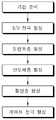
도 1 및 도 2는 본 발명의 일실시예에 따른 트랜지스터의 제조 공정을 개략적으로 나타낸 것이다.1 and 2 schematically show a manufacturing process of a transistor according to an embodiment of the present invention.
탑게이트 형태의 트랜지스터는 기판을 제공하고, 상기 기판 상에 서로 이격되게 소스/드레인 전극을 형성시킨 후, 상기 소스/드레인 전극을 덮도록 반도체층을 형성하고, 상기 반도체층 위에 도펀트층을 형성하며, 상기 도펀트층 상에 절연층을 형성하고, 상기 절연층 상의 일부 영역에 게이트 전극을 형성하는 단계로 구성된다.The top gate type transistor provides a substrate, a source / drain electrode is formed on the substrate so as to be spaced apart from each other, a semiconductor layer is formed to cover the source / drain electrode, a dopant layer is formed on the semiconductor layer Forming an insulating layer on the dopant layer, and forming a gate electrode on a partial region of the insulating layer.
본 발명의 트랜지스터는 n형 반도체 및 p형 반도체가 동시에 구성되는 CMOS 인버터 디바이스에 이용될 수 있다.The transistor of the present invention can be used in a CMOS inverter device in which an n-type semiconductor and a p-type semiconductor are simultaneously formed.
도 1을 참조하면, 기판을 제공하고, 상기 기판 상에 서로 이격되어 있는 소스/드레인 전극을 형성한다.Referring to FIG. 1, a substrate is provided, and source / drain electrodes spaced from each other are formed on the substrate.
상기 기판은 유리와 같은 투명 기판, 실리콘 기판, 플라스틱 기판 또는 금속 포일 기판 등 유연한 기판을 사용할 수 있다. 플라스틱 기판의 예로는 폴리에테르술폰(polyethersulphone), 폴리아크릴레이트(polyacrylate), 폴리에테르 이미드(polyetherimide), 폴리에틸렌 나프탈레이트(polyethyelenen napthalate), 폴리에틸렌테레프탈레이드(polyethyeleneterepthalate), 폴리페닐렌 설파이드(polyphenylene sulfide), 폴리아릴레이트(polyallylate), 폴리이미드(polyimide), 폴리카보네이트(polycarbonate), 셀룰로오스 트리 아세테이트(cellulose triacetate) 및 셀룰로오스 아세테이트 프로피오네이트(cellulose acetate propinoate)등을 이용할 수 있다.The substrate may be a flexible substrate such as a transparent substrate such as glass, a silicon substrate, a plastic substrate, or a metal foil substrate. Examples of plastic substrates include, but are not limited to, polyethersulphone, polyacrylate, polyetherimide, polyethyelenen napthalate, polyethyeleneterepthalate, polyphenylene sulfide, Polyallylate, polyimide, polycarbonate, cellulose triacetate, cellulose acetate propinoate, and the like can be used.
상기 소스/드레인 전극은 Au, Al, Ag, Mg, Ca, Yb, Cs-ITO 또는 이들의 합금 중에서 선택되는 단일층으로 형성될 수 있으며, 기판과의 접착성을 향상시키기 위하여 Ti, Cr 또는 Ni과 같은 접착 금속층을 더욱 포함하여 다중층으로 형성될 수 있다. 또한 그라핀(graphene), 카본나노튜브(CNT), PEDOT:PSS 전도성 고분자 실버나노와이어(silver nanowire) 등을 이용하여 기존의 금속보다 탄성에 더욱 유연한 소자를 제조할 수 있으며 위 물질들을 잉크로 사용하여 잉크젯 프린팅 또는 스프레이 등의 인쇄공정을 이용하여 소스/드레인 전극을 제조할 수 있다. 이러한 인쇄공정을 통해서 소스/드레인 전극을 형성하며 진공공정을 배제할 수 있어서 제조비용의 절감효과를 기대할 수 있다.The source / drain electrodes may be formed of a single layer selected from Au, Al, Ag, Mg, Ca, Yb, Cs-ITO or alloys thereof. In order to improve adhesion with the substrate, And may further include an adhesive metal layer such as a metal layer. In addition, by using graphene, carbon nanotube (CNT), PEDOT: PSS conductive polymer silver nanowire, etc., it is possible to fabricate a more flexible device than the existing metal and use the above materials as ink A source / drain electrode can be manufactured using a printing process such as inkjet printing or spraying. Since the source / drain electrodes are formed through the printing process and the vacuum process can be eliminated, the manufacturing cost can be expected to be reduced.
상기 소스/드레인 전극 상에는 반도체층을 형성할 수 있다. 상기 반도체층은 유기반도체, 금속산화물 반도체, 탄소화합물 반도체 중 어느 하나로 이루어질 수 있다.A semiconductor layer may be formed on the source / drain electrodes. The semiconductor layer may be formed of any one of an organic semiconductor, a metal oxide semiconductor, and a carbon compound semiconductor.
상기 유기반도체는 양쪽성 유기반도체, n형 유기반도체 또는 p형 유기반도체를 이용할 수 있다.The organic semiconductor may be an amphoteric organic semiconductor, an n-type organic semiconductor, or a p-type organic semiconductor.
상기 양쪽성 유기반도체로는 PCBM([6,6]-phenyl-C61-butyric acid methyl ester), P(NDI2OD-T2) (Naphthalene-bis(dicarboximide) bithiophene), F8BT (poly[(9,9-di-n-octylfluorenyl-2,7-diyl)-alt-(benzo[2,1,3]thiadiazol-4,8-diyl)]), PFO (poly(9,9-dioctylfluorene)), DPPT-TT(diketopyrrolo-pyrrole-bithiophene) 및 PTVPhI-Eh (poly(thienylenevinylene-cophthalimide) functionalized with dodecyl at the imide nitrogen) 중 어느하나를 이용할 수 있다.Examples of the amphiphilic organic semiconductor include PCBM ([6,6] -phenyl-C61-butyric acid methyl ester), P (NDI2OD-T2) (Naphthalene-bis (dicarboximide) bithiophene), F8BT (poly [ di-n-octylfluorenyl-2,7-diyl) -tallow- (benzo [2,1,3] thiadiazol-4,8-diyl)], PFO (poly (9,9-dioctylfluorene) (diketopyrrolopyrrole-bithiophene) and PTVPhI-Eh (poly (thienylenevinylene-cophthalimide) functionalized with dodecyl at the imide nitrogen).
상기 n형 반도체는 아센계 물질, 완전 불화된 아센계 물질, 부분 불화된 아센계 물질, 부분 불화된 올리고티오펜(oligothiophene)계 물질, 플러렌(fullerene)계 물질, 치환기를 갖는 플러렌계 물질, 완전 불화된 프탈로시아닌(phthalocyanine)계 물질, 부분 불화된 프탈로시아닌계 물질, 페릴렌 테트라카르복실릭 디이미드(perylene tetracarboxylic diimide)계 물질, 페릴렌 테트라카르복실 디안하이드라이드(perylene tetracarboxylic dianhydride)계 물질, 나프탈렌 테트라카르복실릭 디이미드(naphthalene tetracarboxylic diimide)계 물질 또는 나프탈렌 테트라카르복실릭 디안하이드라이드(naphthalene tetracarboxylic dianhydride)계 물질 중에서 어느 하나를 선택할 수 있다. 여기서 상기 아센(acene)계 물질은 안트라센, 테트라센, 펜타센, 페릴렌 또는 코노렌 중에서 선택될 수 있다.The n-type semiconductor may be selected from the group consisting of an acetal material, a completely fluorinated acetal material, a partially fluorinated acetal material, a partially fluorinated oligothiophene material, a fullerene material, a substituent fullerene material, A perfluorinated tetracarboxylic dianhydride-based material, a perylene tetracarboxylic dianhydride-based material, a naphthalene tetra-carboxylic acid dianhydride-based material, a fluorinated tetracarboxylic dianhydride- A naphthalene tetracarboxylic dianhydride-based material or a naphthalene tetracarboxylic dianhydride-based material may be selected. Here, the acene-based material may be selected from anthracene, tetracene, pentacene, perylene, or quinoline.
또한 상기 p형 유기반도체는 아센(acene), 폴리-티에닐렌비닐렌(poly-thienylenevinylene), 폴리-3-헥실티오펜(poly-3-hexylthiophen), 알파-헥사티에닐렌(α-hexathienylene), 나프탈렌(naphthalene), 알파-6-티오펜(α-6-thiophene), 알파-4-티오펜 (α-4-thiophene), 루브렌(rubrene), 폴리티오펜(polythiophene), 폴리파라페닐렌비닐렌 (polyparaphenylenevinylene), 폴리파라페닐렌(polyparaphenylene), 폴리티오펜비닐렌(polythiophenevinylene), 폴리티오펜-헤테로고리방향족 공중합체(polythiophene-heterocyclicaromatic copolymer), 트리아릴아민(triarylamine)을 포함하는 물질 또는 이들의 유도체 중에서 선택될 수 있는 데, 여기서 상기 아센족 물질은 펜타센(pentacene), 페릴렌(perylene), 테트라센(tetracene) 또는 안트라센(anthracene) 중에서 어느 하나이다.The p-type organic semiconductor may be one selected from the group consisting of acene, poly-thienylenevinylene, poly-3-hexylthiophen, alpha -hexathienylene, Naphthalene, alpha-6-thiophene, alpha-4-thiophene, rubrene, polythiophene, polyparaphenylene A material comprising polyparaphenylenevinylene, polyparaphenylene, polythiophenevinylene, polythiophene-heterocyclicaromatic copolymer, triarylamine or the like, And the derivatives thereof may be selected from the group consisting of pentacene, perylene, tetracene, and anthracene.
또한, 상기 금속산화물 반도체는 아연산화물(ZnOx), 인듐산화물(InOx), 인듐갈륨아연산화물(IGZO), 인듐주석산화물(ITO) 중 어느 하나로 선택될 수 있다.The metal oxide semiconductor may be selected from any one of zinc oxide (ZnOx), indium oxide (InOx), indium gallium zinc oxide (IGZO), and indium tin oxide (ITO).
또한, 상기 탄소화합물 반도체는 반도체성 탄소나노튜브(CNT) 또는 그래핀(Graphene) 나노리본으로부터 이용할 수 있다.
In addition, the carbon compound semiconductor may be used from semiconducting carbon nanotubes (CNTs) or graphene nanoribbons.
상기 반도체층은 스핀코팅, 스프레이(Spray), 잉크젯(Inkjet), 플렉소그라피(Flexography), 스크린(Screen), DipCoating 및 Gravure 등의 방법을 통해 소스/드레인 전극위에 형성된다. 이는 전극 상 및 기판의 국부적인 영역에 패턴을 형성할 수 있으며, 유기반도체층 형성 후 반도체 결정성 및 안정성 등의 소자 성능을 향상시키기 위해 열처리나 광학적 노출(exposure) 등을 시행할 수 있다.
The semiconductor layer is formed on the source / drain electrodes by a method such as spin coating, spraying, inkjet, flexography, screen, Dip Coating, and Gravure. This can form a pattern on the electrode and a local area of the substrate. After the formation of the organic semiconductor layer, heat treatment or optical exposure can be performed to improve device performance such as semiconductor crystallinity and stability.
다음으로 본 발명은 유기반도체층이 형성된 부위에 선택적으로 일부분에 도펀트를 형성할 수 있다.(도펀트층 형성단계)Next, the present invention can selectively form a dopant on a portion where the organic semiconductor layer is formed (dopant layer forming step).
도펀트층의 형성은 도펀트를 포함한 용매가 반도체층을 녹여 반도체층의 일부분을 차지하는 영역을 도펀트층으로 형성되는 것을 의미한다.The formation of the dopant layer means that the solvent including the dopant dissolves the semiconductor layer to form a dopant layer in a region occupying a part of the semiconductor layer.
이때 반도체층의 일부분에 도펀트를 형성하기 위해서 잉크젯 프린팅을 이용한다.At this time, inkjet printing is used to form a dopant in a part of the semiconductor layer.
잉크젯 프린팅으로 전극, 반도체층의 형성 등 소자를 형성하는 기술은 다수 이용되었으나, 본 발명에서는 필요없는 부위를 제거하는 소위 도펀트층 형성 공정은 용매를 잉크로 하는 잉크젯 프린팅으로 도펀트를 형성할 수 있다.Many techniques for forming an electrode and a semiconductor layer by ink jet printing have been used. In the present invention, a so-called dopant layer forming process for removing unnecessary portions can form a dopant by inkjet printing using a solvent as an ink.
본 발명은 상기 잉크젯 프린팅으로 도펀트층을 형성할 수 있는 데, 국소부위만을 형성할 수 있어서 현재 잉크젯 프린팅을 이용하여 기술적으로 가능한 영역까지 국소적으로 실시할 수 있다. 작게는 1㎛ 내외에서 크게는 원하는 영역까지 도펀트층의 형성이 가능하다. 바람직하게는 1㎛ 내지 10mm 의 크기를 갖도록 도펀트층을 형성할 수 있다. 반도체층 상에 도펀트층을 선택적으로 형성하기 위해서는 다른 인쇄공정을 이용하기는 기술적으로 힘들고, 잉크젯 프린팅 기법만으로 이러한 공정을 실시할 수 있다.
In the present invention, the dopant layer can be formed by the inkjet printing, and only a local region can be formed. Thus, the present invention can be locally performed to a technically possible region using inkjet printing. It is possible to form the dopant layer from about 1 mu m to as large as the desired region. The dopant layer may be formed to have a size of preferably 1 to 10 mm. In order to selectively form a dopant layer on the semiconductor layer, it is technically difficult to use another printing process, and such a process can be performed only by an inkjet printing technique.
본 발명에 있어서 도펀트로 이용할 수 있는 물질은 n형 도펀트 또는 p형 도펀트를 이용할 수 있다.In the present invention, an n-type dopant or a p-type dopant can be used as the dopant.
n형 도펀트로는 CsF(Cesium Fluoride), BEDT-TTF (bis(ethylenedithio)-tetrathiafulvalene), TTN (tetrathianaphthacene), CoCp2 (bis(cyclopentadienyl)-cobalt(II)), Cr2(hpp)4 (chromium with the anion of 1,3,4,6,7,8-hexahydro-2H-pyrimido[1,2-a]pyrimidine (hpp)), W2(hpp)4 (tungsten with the anion of 1,3,4,6,7,8-hexahydro-2H-pyrimido[1,2-a]pyrimidine (hpp)), pyronin B chloride, acridine orange base [3,6-bis(dimethylamino)acridine (AOB)], leuco bases like leuco crystal violet (LCV), (nDMBI) (4-(1,3-dimethyl-2,3-dihydro-1H-benzoimidazol-2 yl)phenyl)dimethylamine, (o-MeO-DMBI-I) 2-(2-methoxyphenyl)-1,3-dimethyl-1H-benzoimidazol-3-ium iodide 등을 이용할 수 있다.Examples of the n-type dopant include CsF (Cesium Fluoride), BEDT-TTF (bis (ethylenedithio) -tetrathiafulvalene), TTN (tetrathianaphthacene), CoCp2 (bis (cyclopentadienyl) -cobalt anion of 1,3,4,6,7,8-hexahydro-2H-pyrimido [1,2-a] pyrimidine (hpp)), W2 (hpp) 4 (tungsten with the anion of 1,3,4,6 , 7,8-hexahydro-2 H -pyrimido [1,2-a] pyrimidine (hpp)), pyronin B chloride, acridine orange base [3,6-bis (dimethylamino) acridine (AOB)], leuco bases like leuco crystal (LCV), (nDMBI) (4- (1,3-dimethyl-2,3-dihydro-1H-benzoimidazol-2-yl) phenyl) dimethylamine, 2- (2-methoxyphenyl) ) -1,3-dimethyl-1H-benzoimidazol-3-ium iodide.
p형 도펀트로는 F4-TCNQ (2,3,5,6-tetrafluoro-7,7,8,8-tetracyanoquinodimethane), F2-HCNQ (3,6-difluoro-2,5,7,7,8,8-hexacyanoquinodimethane), MoO3 (Molybdenum trioxide), WO3 (Tungsten trioxide) 등을 이용할 수 있다.Examples of the p-type dopant include F4-TCNQ (2,3,5,6-tetrafluoro-7,7,8,8-tetracyanoquinodimethane), F2-HCNQ (3,6-difluoro-2,5,7,7,8- 8-hexacyanoquinodimethane), MoO3 (Molybdenum trioxide), WO3 (tungsten trioxide), and the like.
한편 도펀트를 잉크젯 프린팅을 이용하여 인쇄하려면, 도펀트를 녹일 수 있는 용매가 필요한 데, 상기 용매의 특징은 도펀트를 모두 녹일 수 있으며, 반도체층의 일부를 녹이는 것이 바람직하다.On the other hand, in order to print a dopant using inkjet printing, a solvent capable of dissolving a dopant is required. The solvent is characterized in that it can dissolve all of the dopant and dissolve a part of the semiconductor layer.
사용가능한 용매로는 클로로벤젠(Chlorobenzene), 클로로포름(Chloroform), 트리클로로벤젠(Trichlorobenzene), 테트라히드로퓨란(Tetrahydrofuran), 디클로로벤젠(Dichlorobenzene), 디클로로에탄(Dichloroethane) 등과 같은 용매를 이용할 수 있다.Examples of usable solvents include solvents such as chlorobenzene, chloroform, trichlorobenzene, tetrahydrofuran, dichlorobenzene, and dichloroethane.
잉크젯으로 프린팅 할 때 도펀트가 용매에 혼합되는 비율은 0.5mg/ml ~ 1.5mg/ml%인 것이 바람직하다.The proportion of the dopant mixed with the solvent when printing with an inkjet is preferably 0.5 mg / ml to 1.5 mg / ml%.
일반적으로 반도체에 비해 도펀트의 비율이 0.5mg/ml보다 작을 때에는 효과적으로 도핑이 이루어지지 않아 소자성능의 변화가 일어나지 않을 수 있거나 미비할 수 있으며, 도펀트의 비율이 1.5mg/ml를 초과할 때에는 반도체 박막의 결정성에 악영향을 끼쳐 소자의 성능을 감소시키거나, 전도도가 너무 상승해 트랜지스터로 동작을 하는데 문제가 될 수 있다.
Generally, when the ratio of the dopant is less than 0.5 mg / ml as compared with the semiconductor, doping is not effectively performed, and the device performance may or may not change. When the dopant ratio exceeds 1.5 mg / ml, The crystallinity of the device may be adversely affected to reduce the performance of the device, or the conductivity may become too high to operate as a transistor.
도 2를 참조하면, CMOS 인버터 디바이스를 제조하는 경우 전극상에 반도체층을 형성하고 반도체층의 일부에 도펀트를 형성할 수 있는 데, 2곳의 S/D 전극 사이 반도체층상에 도펀트를 형성할 수 있다. 도 2에서 보는 바와 같이 한곳의 S/D 전극 사이 반도체층상에는 n형 도펀트를 다른 한곳의 S/D 전극 사이 반도체층상에는 p형 도펀트를 인쇄할 수 있는 데, 도펀트를 녹일 수 있는 용매를 반도체상에 인쇄하여 반도체층을 일부 녹도록 하여 도펀트가 반도체층에 혼합되도록 하는 것이 바람직하다.Referring to FIG. 2, when a CMOS inverter device is manufactured, a semiconductor layer may be formed on an electrode and a dopant may be formed on a part of the semiconductor layer. A dopant may be formed on the semiconductor layer between two S / have. 2, an n-type dopant can be printed on one semiconductor layer between the S / D electrodes and a p-type dopant can be printed on the other semiconductor layer between the S / D electrodes. The solvent capable of dissolving the dopant can be printed on the semiconductor layer So that the semiconductor layer is partially melted so that the dopant is mixed with the semiconductor layer.
반도체층 중에서 도펀트가 포함되어 있는 부분에서의 도펀트의 양은 0.5질량% ~ 1.0질량%인 것이 바람직하다.The amount of the dopant in the portion of the semiconductor layer containing the dopant is preferably 0.5% by mass to 1.0% by mass.
반도체층 중에서 도펀트가 포함되어 있는 부분에서의 도펀트의 양은 0.5질량% ~ 1.0질량%인 것이 바람직하다.The amount of the dopant in the portion of the semiconductor layer containing the dopant is preferably 0.5% by mass to 1.0% by mass.
도펀트의 양이 0.5질량% ~ 1.0질량%일 때 소자의 성능이 우수하게 되는 데, 반도체 박막의 결정성에 악영향을 끼치지 않으며 우수한 전도도가 나타나게 된다.
When the amount of the dopant is 0.5% by mass to 1.0% by mass, the performance of the device is excellent, and the crystalline property of the semiconductor thin film is not adversely affected and excellent conductivity is exhibited.
도 3은 반도체층에 포함되는 도펀트의 양에 따른 이동도 추이 및 전압 변화를 나타낸 것이다.3 shows the mobility and the voltage change according to the amount of the dopant included in the semiconductor layer.
도 3의 (a)는 n도핑과 p도핑으로 인하여 변화하는 전자와 정공의 전하이동도의 추이를 나타내고, (b)는 이에 따른 시작전압 (Von)의 변화를 나타낸다.3 (a) shows the change in the charge mobility of electrons and holes that change due to n-doping and p-doping, and FIG. 3 (b) shows the change in the start voltage Von.
도 3의 (a)에서 볼 수 있듯이 도핑을 하지 않았을 때에는 전하와 정공의 이동도가 비슷한 양방향성 전달 특성을 나타낸다. 그러나 n도핑을 하였을 경우에는 n형 특성이 증가하는 반면 p형 특성이 감소하여 n형 트랜지스터 특성을 보이게 된다. 또한 p형 도펀트를 첨가하였을 때는 p형 특성이 증가하는 반면 n형 특성이 감소하여 p형 트랜지스터 특성을 보인다.As shown in FIG. 3 (a), when doping is not performed, the charge and hole mobility show a similar bi-directional transfer characteristic. However, when n-doping is performed, the n-type characteristics are increased, while the p-type characteristics are decreased to show the characteristics of the n-type transistor. In addition, when p type dopant is added, the p type characteristics are increased while the n type characteristics are decreased to show the characteristics of p type transistors.
또한 도 3의 (b)에서 알 수 있듯이, 도핑으로 인하여 트랜지스터의 시작 전압을 조절할 수 있다. n형 도펀트의 양이 증가할수록 n형 트랜지스터의 시작전압이 낮아지고, p형 도펀트의 양이 증가할 수록 p형 트랜지스터의 시작전압이 낮아진다. 즉 도펀트의 유형과 양을 조절을 통하여 트랜지스터의 성능을 원하는 방향으로 변화시킬 수 있다.
Also, as can be seen from FIG. 3 (b), the start voltage of the transistor can be adjusted by doping. As the amount of the n-type dopant increases, the starting voltage of the n-type transistor decreases. As the amount of the p-type dopant increases, the starting voltage of the p-type transistor decreases. That is, by adjusting the type and amount of the dopant, the performance of the transistor can be changed to a desired direction.
한편, 상기 도펀트층이 인쇄된 유기반도체층 상의 전면에 걸쳐서는 절연층을 형성할 수 있다. (절연층 형성단계)On the other hand, an insulating layer may be formed over the entire surface of the organic semiconductor layer on which the dopant layer is printed. (Insulating layer forming step)
유기절연층 또는 무기절연층의 단일막 또는 다층막으로 포함되거나 유-무기 하이브리드 막으로 포함된다. 상기 유기절연층으로는 폴리메타아크릴레이트 (PMMA, polymethylmethacrylate), 폴리스타이렌(PS, polystyrene), 페놀계 고분자, 아크릴계 고분자, 폴리이미드와 같은 이미드계 고분자, 아릴에테르계 고분자, 아마이드계 고분자, 불소계 고분자, p자일리렌계 고분자, 비닐알콜계 고분자, 파릴렌(parylene) 중에서 1이상 선택될 수 있다. 상기 무기절연층으로는 실리콘 산화막, 실리콘 질화막, Al2O3, Ta2O5, BST, PZT 중에서 1이상 선택될 수 있다.An organic insulating layer or an inorganic insulating layer, or as a organic-inorganic hybrid film. The organic insulating layer may be an imide polymer such as polymethylmethacrylate (PMMA), polystyrene (PS), a phenolic polymer, an acrylic polymer, or a polyimide, an arylether polymer, an amide polymer, p-xylylene-based polymer, vinyl alcohol-based polymer, and parylene. The inorganic insulating layer may be at least one selected from the group consisting of a silicon oxide film, a silicon nitride film, Al2 O3 , Ta2 O5 , BST and PZT.
상기 절연층 상의 일부영역에는 게이트 전극을 형성할 수 있다. (게이트 전극 형성단계)A gate electrode may be formed on a part of the insulating layer. (Gate electrode forming step)
상기 게이트 전극은 알루미늄(Al), 알루미늄 합금(Al-alloy), 몰리브덴(Mo), 몰리브덴 합금(Mo-alloy), 실버나노와이어(silver nanowire), 갈륨인듐유태틱(gallium indium eutectic), PEDOT;PSS 중에서 선택되는 어느 하나로 형성할 수 있다. 상기 게이트 전극은 위 물질들을 잉크로 사용하여 잉크젯 프린팅 또는 스프레이 등의 인쇄공정을 이용하여 게이트 전극을 제조할 수 있다. 이러한 인쇄공정을 통해서 게이트 전극을 형성하며 진공공정을 배제할 수 있어서 제조비용의 절감효과를 기대할 수 있다.The gate electrode may be formed of one selected from the group consisting of aluminum (Al), aluminum alloy (Al), molybdenum (Mo), molybdenum alloy, silver nanowire, gallium indium eutectic, PEDOT; PSS and the like. The gate electrode can be manufactured using a printing process such as inkjet printing or spraying using the above materials as an ink. Since the gate electrode is formed through the printing process and the vacuum process can be eliminated, the manufacturing cost can be expected to be reduced.
이로써 본 발명의 일실시예에 따른 트랜지스터를 완성할 수 있다.
Thus, the transistor according to an embodiment of the present invention can be completed.
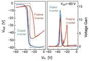
도 4는 본 발명의 일실시예에 따라 제조된 CMOS 인버터와 도펀트를 인쇄하지 않은 CMOS 인버터의 성능을 비교한 그래프이다.4 is a graph comparing the performance of a CMOS inverter manufactured according to an embodiment of the present invention and a CMOS inverter not having a dopant printed thereon.
도 4는 CMOS 인버터의 전압-전달특성(왼쪽)과 전압이익특성(오른쪽)을 각각 나타낸다. 도핑을 하지 않은 것은 그래프에서 주황색으로 표현하였는 데 이경우 Vin= -60V 일 때와 0V일 때 전압손실이 각각 5V 와 20V 이상이 나타났다. 이는 큰 전력 손실 [P(전력손실) = V (전압) * I (전류)]과 낮은 전압 여유 (Noise Margin)을 가져오게 된다. 또한 큰 히스테리시스를 보이는데 이러한 소자는 실제로 회로에 사용될 때 안정성 등에 문제가 될 수 있다.4 shows voltage-transfer characteristics (left) and voltage gain characteristics (right) of a CMOS inverter, respectively. In the case of Vin = -60V and 0V, the voltage loss was 5V and 20V or more, respectively. This results in a large power loss [P (power loss) = V (voltage) * I (current)] and a low voltage margin (noise margin). They also exhibit large hysteresis, which can be a problem with stability when actually used in a circuit.
이에 반해 잉크젯 프린팅으로 도핑이 이루어진 본 발명은 그래프에서 파란색으로 표현하였는 데, 이 경우 도핑을 하지 않는 인버터의 그래프에 비해 Vin = -60V 일 때와 0V 일 때 전압손실이 거의 0에 가깝게 낮으며, 히스테리시스가 없는 좋은 인버터 특성을 나타내고 있다. 또한 전압이익특성에서도 도핑을 한 경우 약 14 로써 도핑을 하지 않은 인버터에 비해 높은 값을 보이는 것을 관찰할 수 있다.
On the other hand, in the present invention in which the doping is performed by ink-jet printing, the voltage is expressed in blue in the graph. In this case, when Vin = -60 V and 0 V, the voltage loss is nearly zero, It shows good inverter characteristics without hysteresis. Also, the voltage gain characteristic is about 14 in the case of doping, which is higher than that of the non-doped inverter.
이하, 본 발명의 구체적인 실시예에 대하여 자세히 설명한다.Hereinafter, specific embodiments of the present invention will be described in detail.
실시예 1Example 1
기판준비 및 전극형성Substrate preparation and electrode formation
트랜지스터를 제조하는 데 있어, 기판을 준비하고, 상기 기판 상에 소스/드레인 전극을 형성한다.
In fabricating the transistor, a substrate is prepared and a source / drain electrode is formed on the substrate.
반도체층 형성Semiconductor layer formation
유기반도체층 형성은 유기반도체인 PCBM을 이용하여 유기반도체층을 형성하였다. 유기반도체층의 형성은 S전극과 D전극을 모두 덮도록 반도체층을 형성하였다.
The organic semiconductor layer was formed using PCBM, which is an organic semiconductor. In forming the organic semiconductor layer, a semiconductor layer was formed so as to cover both the S electrode and the D electrode.
도펀트층 형성Dopant layer formation
도펀트의 형성을 위해서 용매 클로로벤젠을 준비하여 n형 도펀트를 혼합하여 n형 도펀트 용액을 제조한다. n형 도펀트로는 CsF(Cesium Fluoride)를 이용하며, 도펀트의 농도가 각각 1mg/ml가 되도록 제조하였다.A solvent chlorobenzene is prepared for the formation of a dopant and an n-type dopant is mixed to prepare an n-type dopant solution. As the n-type dopant, CsF (Cesium Fluoride) was used and the dopant concentration was 1 mg / ml.
이를 잉크젯 프린팅을 이용하여 반도체층상에 인쇄를 하는 데, S전극 및 D전극의 중간영역의 반도체층상에 n형 도펀트인 CsF를 이용하여 도펀트층을 형성하였다. 잉크젯 프린팅시 지름은 약 50㎛가 되도록 인쇄하여 도펀트를 도핑하였다.In printing on the semiconductor layer using inkjet printing, a dopant layer was formed using CsF as an n-type dopant on the semiconductor layer in the middle region between the S electrode and the D electrode. In the case of inkjet printing, the diameter was printed to be about 50 탆 and the dopant was doped.
도펀트가 주입되는 반도체층의 도펀트양이 1.0질량%가 되도록 하여 도펀트층을 형성하였다. 이의 제어는 잉트젯 프린팅으로 주입하는 용액의 양을 제어함으로써 조절할 수 있다.
The dopant layer was formed such that the dopant amount of the semiconductor layer into which the dopant was injected was 1.0% by mass. Its control can be controlled by controlling the amount of solution injected by the inkjet printing.
절연층 형성Insulation layer formation
유기반도체층을 포함하여 기판 상부에 형성하는 데, 절연층은 폴리스티렌(PS)를 이용하여 스핀코팅을 이용하여 절연층을 형성하였다.
The organic insulating layer is formed on the substrate including the organic semiconductor layer, and the insulating layer is formed by using spin coating using polystyrene (PS).
게이트 전극 형성Gate electrode formation
절연층 상부의 일부영역에는 게이트 전극을 형성을 형성하는 데, 알루미늄(Al)을 증착에 의하여 형성하였다.Aluminum (Al) was formed by evaporation to form a gate electrode in a part of the upper part of the insulating layer.
상기와 같은 단계를 거쳐 제조한 트랜지스터를 제조하였다.
The transistor fabricated through the above steps was fabricated.
실시예 2 및 실시예 3Examples 2 and 3
실시예 1과 각각 동일하게 실시하되,The same procedure as in Example 1 was repeated,
도펀트층 형성단계에서 도펀트가 주입되는 반도체층의 n형 도펀트인 CsF 도펀트양이 0.5질량%(실시예 2), 0.1질량%(실시예 3)가 되도록 하였다.
The amount of the CsF dopant as the n-type dopant in the semiconductor layer into which the dopant is to be doped was 0.5 mass% (Example 2) and 0.1 mass% (Example 3) in the dopant layer forming step.
실시예 4Example 4
실시예 1과 동일하게 트랜지스터를 제조하되,A transistor was fabricated in the same manner as in Example 1,
도펀트층 형성단계에서 S전극 및 D전극의 중간영역의 반도체층상에 p형 도펀트인 F4-TCNQ를 이용하여 도펀트층을 형성하였다.In the dopant layer formation step, a dopant layer was formed using F4-TCNQ, which is a p-type dopant, on the semiconductor layer in the middle region between the S electrode and the D electrode.
도펀트가 주입되는 반도체층의 도펀트양은 1.0질량%가 되도록 하여 도펀트층을 형성하였다.
The dopant layer was formed so that the amount of the dopant of the semiconductor layer into which the dopant was injected was 1.0% by mass.
실시예 5 및 실시예 6Examples 5 and 6
실시예 4와 각각 동일하게 실시하되,The procedure of Example 4 was repeated,
도펀트층 형성단계에서 도펀트가 주입되는 반도체층의 p형 도펀트인 F4-TCNQ 도펀트양이 0.5질량%(실시예 5), 0.1질량%(실시예 6)가 되도록 하였다.
The amount of the dopant F4-TCNQ, which is the p-type dopant of the semiconductor layer into which the dopant is implanted, is 0.5% by mass (Example 5) and 0.1% by mass (Example 6) in the dopant layer forming step.
비교예 1Comparative Example 1
실시예 1과 동일하게 실시하되, 잉크젯 프린팅을 이용한 도펀트층의 형성없이 박막트랜지서터를 제조하였다.
A thin film transistor was fabricated in the same manner as in Example 1 except that a dopant layer was not formed by inkjet printing.
도 5는 실시예 1, 실시예 4 및 비교예 1의 트랜지스터에서 n채널 및 p채널의 성능을 나타낸 것이다.5 shows the performance of n-channel and p-channel in the transistors of Example 1, Example 4, and Comparative Example 1. FIG.
도 5의 (a)와 (b)는 도펀트를 첨가하기 전의 유기박막 트랜지스터의 p형과 n형의 아웃풋 특성을 나타내고, (c) 는 p형 도펀트가 1.0질랑% 첨가되어진 p형 아웃풋 특성, (d)는 n형 도펀트가 1.0질랑% 첨가되어진 n형 아웃풋 특성을 나타낸다. (a) 와 (b) 그래프에서 알 수 있듯이 도핑이되지 않은 트랜지스터의 경우 드레인 전압 (Vd) 가 낮을 때 전류가 선형적으로 증가하지 못하고 S 자 모양으로 증가하는데 이는 전극과 반도체간의 접촉저항이 높기 때문에 발생하는 안좋은 현상이다. 반면 도핑이 되어진 (c) 와 (d)의 경우에는, Vd가 낮을 때 전류가 선형적으로 증가하며, 도핑이 되지 않았었을 때 비해서 전류가 더 많이 흐르는 것을 알 수 있다. 이는 도핑으로 인해 접촉저항이 상당히 개선되었으며, 반도체 안의 전하의 양이 증가하였기 때문에 소자의 향상이 되었다는 것을 알 수 있다.
5 (a) and 5 (b) show the p-type and n-type output characteristics of the organic thin film transistor before the addition of the dopant, (c) shows the p-type output characteristics with the p- d) shows n-type output characteristics in which 1.0% by weight of n-type dopant is added. As can be seen from the graphs (a) and (b), when the drain voltage (Vd) is low, the current does not increase linearly but increases in S shape. This is a bad phenomenon that occurs. On the other hand, in cases (c) and (d) in which the doping is performed, the current increases linearly when Vd is low, and the current flows more than when doping is not performed. It can be seen that the contact resistance was significantly improved by doping and the device was improved because the amount of charge in the semiconductor was increased.
도 6은 실시예 1 내지 실시예 6 및 비교예 1의 트랜지스터의 성능을 나타낸 것이다.6 shows the performance of the transistors of Examples 1 to 6 and Comparative Example 1.
도 6은 실시예 1 내지 실시예 6 및 비교예 1의 트랜지스터의 전달특성 성능을 비교한 그래프이다. (a)는 n형 도펀트가 첨가된 실시예 1 내지 실시예 3의 p형 특성, (b)는 n형 도펀트가 첨가된 실시예 1 내지 실시예 3의 n형 특성을 나타내며, (c)는 p형 도펀트가 첨가된 실시예 4 내지 실시예 6의 p형 특성, 그리고 (d)는 p형 도펀트가 첨가된 실시예 4 내지 실시예 6의 n형 특성이다.6 is a graph comparing the transfer characteristic performances of the transistors of Embodiments 1 to 6 and Comparative Example 1. FIG. (a) shows p-type characteristics of Examples 1 to 3 in which an n-type dopant is added, (b) shows n-type characteristics of Examples 1 to 3 in which an n-type dopant is added, the p-type characteristics of Examples 4 to 6 in which the p-type dopant was added, and (d) the n-type characteristics of Examples 4 to 6 in which the p-type dopant was added.
도 6의 (a)와 (b)에서 알 수 있듯이, n형 도펀트의 양이 증가할수록 p형 특성에서의 전류는 점점 감소하며, 반대로 n형 특성에서의 전류는 점점 증가하게 된다. 또한 도 6의 (c)와 (d)에서 알 수 있듯이, p형 도펀트가 증가할수록 p형 특성의 전류는 조금 증가하고, 반대로 n형특성은 크게 감소한다. 즉 첨가되는 n형 도펀트의 양이 증가할수록 n형 특성이 좋아지며, p형 도펀트의 양이 증가할록 p형 특성이 좋아지게 됨을 알 수 있다.
As can be seen from FIGS. 6 (a) and 6 (b), as the amount of the n-type dopant increases, the current in the p-type characteristic decreases gradually, while the current in the n-type characteristic increases. As can be seen from (c) and (d) of FIG. 6, as the p-type dopant increases, the current of the p-type current increases slightly and conversely the n-type current decreases. That is, as the amount of the n-type dopant to be added increases, the n-type property improves, and the p-type property to improve the amount of the p-type dopant is improved.
이상에서 설명한 본 발명은 전술한 실시예 및 첨부된 도면에 의해 한정되는 것은 아니고, 본 발명의 기술적 사상을 벗어나지 않는 범위 내에서 여러 가지 치환, 변형 및 변경이 가능함은 본 발명이 속하는 기술분야에서 통상의 지식을 가진 자에게 있어서 명백할 것이다.
It will be apparent to those skilled in the art that various modifications and variations can be made in the present invention without departing from the spirit or scope of the inventions. It will be clear to those who have knowledge of.
Claims (12)
Translated fromKorean상기 도펀트의 형성은 반도체층 형성 후 잉크젯 프린팅을 이용하여 n형 도펀트 또는 p형 도펀트를 선택적으로 인쇄하여 상기 반도체층의 일부분을 차지하도록 하는 데, 상온에서 도펀트를 포함한 용매가 반도체층을 녹여 반도체층의 일부분을 차지하도록 하며,
상기 도펀트는 n형 도펀트로 CsF(Cesium Fluoride), BEDT-TTF (bis(ethylenedithio)-tetrathiafulvalene), TTN (tetrathianaphthacene), CoCp2 (bis(cyclopentadienyl)-cobalt(II)), Cr2(hpp)4 (chromium with the anion of 1,3,4,6,7,8-hexahydro-2H-pyrimido[1,2-a]pyrimidine (hpp)), W2(hpp)4 (tungsten with the anion of 1,3,4,6,7,8-hexahydro-2H-pyrimido[1,2-a]pyrimidine (hpp)), pyronin B chloride, acridine orange base [3,6-bis(dimethylamino)acridine (AOB)], leuco bases like leuco crystal violet (LCV), (nDMBI) (4-(1,3-dimethyl-2,3-dihydro-1H-benzoimidazol-2 yl)phenyl)dimethylamine, (o-MeO-DMBI-I) 2-(2-methoxyphenyl)-1,3-dimethyl-1H-benzoimidazol-3-ium iodide 중에서 1이상 선택되며,
p형 도펀트로 F2-HCNQ (3,6-difluoro-2,5,7,7,8,8-hexacyanoquinodimethane), MoO3 (Molybdenum trioxide), WO3 (Tungsten trioxide) 중에서 1이상 선택되는 것을 특징으로 하는 트랜지스터 제조방법.
Forming a semiconductor layer on a substrate for the fabrication of a transistor, forming a dopant on the semiconductor layer,
The dopant is formed by selectively printing an n-type dopant or a p-type dopant by using inkjet printing after forming a semiconductor layer to occupy a portion of the semiconductor layer. At room temperature, a solvent containing a dopant melts the semiconductor layer, , ≪ / RTI >
The dopant may be an n-type dopant selected from the group consisting of CsF (Cesium Fluoride), BEDT-TTF bis (ethylenedithio) -tetrathiafulvalene, TTN tetracathianaphthacene, CoCp2 bis (cyclopentadienyl) (2-a) pyrimidine (hpp)), W2 (hpp) 4 (tungsten with the anion of 1,3,4 , 6,7,8-hexahydro-2H-pyrimido [1,2-a] pyrimidine (hpp)), pyronin B chloride, acridine orange base [3,6-bis (dimethylamino) acridine (LCV), (nDMBI) (4- (1,3-dimethyl-2,3-dihydro-1H-benzoimidazol-2yl) phenyl) dimethylamine, (o- -methoxyphenyl) -1,3-dimethyl-1H-benzoimidazol-3-ium iodide,
wherein at least one of p-type dopant is selected from among 3,6-difluoro-2,5,7,7,8,8-hexacyanoquinodimethane, MoO3 and WO3 (tungsten trioxide) Gt;
상기 n형 도펀트 또는 p형 도펀트는 클로로벤젠(Chlorobenzene), 클로로포름(Chloroform), 트리클로로벤젠(Trichlorobenzene), 테트라히드로퓨란(Tetrahydrofuran), 디클로로벤젠(Dichlorobenzene), 디클로로에탄(Dichloroethane) 중 어느 하나의 용매로 녹여 잉크젯 프린팅에 이용하는 것을 특징으로 하는 것을 특징으로 하는 트랜지스터 제조방법.
The method according to claim 1,
The n-type dopant or the p-type dopant may be at least one selected from the group consisting of chlorobenzene, chloroform, trichlorobenzene, tetrahydrofuran, dichlorobenzene, and dichloroethane , And is used for ink-jet printing.
반도체층 중에서 도펀트가 포함되어 있는 부분에서의 도펀트의 양은 0.5질량% ~ 1.0질량%인 것을 특징으로 하는 트랜지스터 제조방법.
The method according to claim 1,
Wherein an amount of the dopant in the portion of the semiconductor layer containing the dopant is 0.5% by mass to 1.0% by mass.
상기 기판위에 소스/드레인 전극을 형성시키는 S/D전극형성단계;
상기 소스/드레인 전극 상에 반도체층을 형성시키는 반도체층 형성단계;
상기 반도체층의 일부에 도펀트층을 형성하는 단계;
상기 반도체층 상에 절연층을 형성하는 절연층 형성단계; 및
상기 절연층 상에 게이트 전극을 형성시키는 게이트전극 형성단계를 포함하되,
상기 도펀트층 형성은 잉크젯 프린팅을 이용하여 반도체층 상에 인쇄를 통해 선택적으로 형성하되, 반도체층 형성 후 도펀트를 선택적으로 인쇄하여 상기 반도체층의 일부분을 차지하도록 하는 데, 상온에서 도펀트를 포함한 용매가 반도체층을 녹여 반도체층의 일부분을 차지하도록 하며,
상기 도펀트층에 형성되는 도펀트는 n형 도펀트로 CsF(Cesium Fluoride), BEDT-TTF (bis(ethylenedithio)-tetrathiafulvalene), TTN (tetrathianaphthacene), CoCp2 (bis(cyclopentadienyl)-cobalt(II)), Cr2(hpp)4 (chromium with the anion of 1,3,4,6,7,8-hexahydro-2H-pyrimido[1,2-a]pyrimidine (hpp)), W2(hpp)4 (tungsten with the anion of 1,3,4,6,7,8-hexahydro-2H-pyrimido[1,2-a]pyrimidine (hpp)), pyronin B chloride, acridine orange base [3,6-bis(dimethylamino)acridine (AOB)], leuco bases like leuco crystal violet (LCV), (nDMBI) (4-(1,3-dimethyl-2,3-dihydro-1H-benzoimidazol-2 yl)phenyl)dimethylamine, (o-MeO-DMBI-I) 2-(2-methoxyphenyl)-1,3-dimethyl-1H-benzoimidazol-3-ium iodide 중에서 1이상 선택되며,
p형 도펀트로 F2-HCNQ (3,6-difluoro-2,5,7,7,8,8-hexacyanoquinodimethane), MoO3 (Molybdenum trioxide), WO3 (Tungsten trioxide) 중에서 1이상 선택되는 것을 특징으로 하는 트랜지스터 제조방법.
Preparing a substrate;
An S / D electrode forming step of forming a source / drain electrode on the substrate;
A semiconductor layer forming step of forming a semiconductor layer on the source / drain electrodes;
Forming a dopant layer on a part of the semiconductor layer;
An insulating layer forming step of forming an insulating layer on the semiconductor layer; And
And forming a gate electrode on the insulating layer,
The dopant layer is selectively formed on the semiconductor layer by printing using inkjet printing. The dopant is selectively printed after the semiconductor layer is formed to occupy a portion of the semiconductor layer. Dissolving the semiconductor layer to occupy a portion of the semiconductor layer,
The dopant to be formed in the dopant layer may be an n-type dopant such as CsF (Cesium Fluoride), BEDT-TTF (bis (ethylenedithio) -tetrathiafulvalene), TTN (tetrathianaphthacene), CoCp2 (bis (cyclopentadienyl) (hpp) 4 (chromium with the anion of 1,3,4,6,7,8-hexahydro-2H-pyrimido [1,2-a] pyrimidine 1,3,6,7,8-hexahydro-2H-pyrimido [1,2-a] pyrimidine (hpp)), pyronin B chloride, acridine orange base [3,6- bis (dimethylamino) acridine ), leuco bases like leuco crystal violet (LCV), (nDMBI) (4- (1,3-dimethyl-2,3-dihydro-1H-benzoimidazol- ) 2- (2-methoxyphenyl) -1,3-dimethyl-1H-benzoimidazol-3-ium iodide,
wherein at least one of p-type dopant is selected from among 3,6-difluoro-2,5,7,7,8,8-hexacyanoquinodimethane, MoO3 and WO3 (tungsten trioxide) Gt;
상기 n형 도펀트 또는 p형 도펀트는 클로로벤젠(Chlorobenzene), 클로로포름(Chloroform), 트리클로로벤젠(Trichlorobenzene), 테트라히드로퓨란(Tetrahydrofuran), 디클로로벤젠(Dichlorobenzene), 디클로로에탄(Dichloroethane) 중 어느 하나의 용매로 녹여 잉크젯 프린팅에 이용하는 것을 특징으로 하는 것을 특징으로 하는 트랜지스터 제조방법.
6. The method of claim 5,
The n-type dopant or the p-type dopant may be at least one selected from the group consisting of chlorobenzene, chloroform, trichlorobenzene, tetrahydrofuran, dichlorobenzene, and dichloroethane , And is used for ink-jet printing.
도펀트층 형성단계에서 도펀트의 양은 0.5질량% ~ 1.0질량%가 포함된 것을 특징으로 하는 트랜지스터 제조방법.
6. The method of claim 5,
Wherein the amount of the dopant in the dopant layer formation step is from 0.5 mass% to 1.0 mass%.
상기 반도체층은 유기반도체, 금속산화물 반도체 및 탄소화합물 반도체 중 어느 하나로 이루어지는 것을 특징으로 하는 트랜지스터 제조방법.
6. The method of claim 5,
Wherein the semiconductor layer is made of any one of an organic semiconductor, a metal oxide semiconductor, and a carbon compound semiconductor.
상기 유기반도체는 양쪽성 유기반도체, n형 유기반도체 및 p형 유기반도체 중 어느 하나로 이루어지며,
상기 양쪽성 유기반도체는 PCBM([6,6]-phenyl-C61-butyric acid methyl ester), P(NDI2OD-T2) (Naphthalene-bis(dicarboximide) bithiophene), F8BT (poly[(9,9-di-n-octylfluorenyl-2,7-diyl)-alt-(benzo[2,1,3]thiadiazol-4,8-diyl)]), PFO (poly(9,9-dioctylfluorene)), DPPT-TT(diketopyrrolo-pyrrole-bithiophene) 및 PTVPhI-Eh (poly(thienylenevinylene-cophthalimide) functionalized with dodecyl at the imide nitrogen) 중 어느하나로 선택되고,
상기 n형 유기 반도체는 아센계 물질, 완전 불화된 아센계 물질, 부분 불화된 아센계 물질, 부분 불화된 올리고티오펜(oligothiophene)계 물질, 플러렌(fullerene)계 물질, 치환기를 갖는 플러렌계 물질, 완전 불화된 프탈로시아닌(phthalocyanine)계 물질, 부분 불화된 프탈로시아닌계 물질, 페릴렌 테트라카르복실릭 디이미드(perylene tetracarboxylic diimide)계 물질, 페릴렌 테트라카르복실 디안하이드라이드(perylene tetracarboxylic dianhydride)계 물질, 나프탈렌 테트라카르복실릭 디이미드(naphthalene tetracarboxylic diimide)계 물질 및 나프탈렌 테트라카르복실릭 디안하이드라이드(naphthalene tetracarboxylic dianhydride)계 물질 중에서 어느 하나로 선택되며,
상기 p형 유기반도체는 아센(acene), 폴리-티에닐렌비닐렌(poly-thienylenevinylene), 폴리-3-헥실티오펜(poly-3-hexylthiophen), 알파-헥사티에닐렌(α-hexathienylene), 나프탈렌(naphthalene), 알파-6-티오펜(α-6-thiophene), 알파-4-티오펜 (α-4-thiophene), 루브렌(rubrene), 폴리티오펜(polythiophene), 폴리파라페닐렌비닐렌 (polyparaphenylenevinylene), 폴리파라페닐렌(polyparaphenylene), 폴리티오펜비닐렌(polythiophenevinylene), 폴리티오펜-헤테로고리방향족 공중합체(polythiophene-heterocyclicaromatic copolymer), 트리아릴아민(triarylamine) 중에서 어느하나로 선택되는 것을 특징으로 하는 트랜지스터 제조방법.
10. The method of claim 9,
Wherein the organic semiconductor is made of any one of an amphoteric organic semiconductor, an n-type organic semiconductor and a p-type organic semiconductor,
The amphiphilic organic semiconductor may be selected from the group consisting of PCBM ([6,6] -phenyl-C61-butyric acid methyl ester), P (NDI2OD-T2) (Naphthalene-bis (dicarboximide) bithiophene), F8BT -n-octylfluorenyl-2,7-diyl) -tallow- (benzo [2,1,3] thiadiazol-4,8-diyl)], PFO (poly (9,9-dioctylfluorene)), DPPT- diketopyrrolo-pyrrole-bithiophene) and PTVPhI-Eh (poly (thienylenevinylene-cophthalimide) functionalized with dodecyl at the imide nitrogen)
The n-type organic semiconductor may be selected from the group consisting of an acetone-based material, a completely fluorinated acetal-based material, a partially fluorinated acetal-based material, a partially fluorinated oligothiophene- based material, a fullerene- A partially fluorinated phthalocyanine-based material, a perylene tetracarboxylic diimide-based material, a perylene tetracarboxylic dianhydride-based material, a naphthalene-based material, a perylene tetracarboxylic dianhydride- A naphthalene tetracarboxylic dianhydride-based material and a naphthalene tetracarboxylic dianhydride-based material, wherein the naphthalene tetracarboxylic dianhydride-
The p-type organic semiconductor may be one selected from the group consisting of acene, poly-thienylenevinylene, poly-3-hexylthiophen, alpha -hexathienylene, naphthalene, alpha-6-thiophene, alpha-4-thiophene, rubrene, polythiophene, polyparaphenylene vinyl A compound selected from any one of polyparaphenylenevinylene, polyparaphenylene, polythiophenevinylene, polythiophene-heterocyclicaromatic copolymer, and triarylamine. Wherein the transistor is fabricated.
상기 금속산화물 반도체는 아연산화물(ZnOx), 인듐산화물(InOx), 인듐갈륨아연산화물(IGZO), 인듐주석산화물(ITO) 산화물 중 어느 하나로 선택되는 것을 특징으로 하는 트랜지스터 제조방법.10. The method of claim 9,
Wherein the metal oxide semiconductor is selected from any one of zinc oxide (ZnOx), indium oxide (InOx), indium gallium zinc oxide (IGZO), and indium tin oxide (ITO) oxide.
상기 탄소화합물 반도체는 반도체성 탄소나노튜브(CNT) 또는 그래핀(Graphene) 나노리본으로부터 선택되는 트랜지스터 제조방법.10. The method of claim 9,
Wherein the carbon compound semiconductor is selected from semiconducting carbon nanotubes (CNT) or graphene nanoribbons.
Priority Applications (3)
| Application Number | Priority Date | Filing Date | Title |
|---|---|---|---|
| KR1020140090254AKR101616190B1 (en) | 2014-07-17 | 2014-07-17 | Manufacturing method of transitor using selective print of dopant |
| US15/320,750US9997709B2 (en) | 2014-07-17 | 2015-07-14 | Method for manufacturing transistor according to selective printing of dopant |
| PCT/KR2015/007283WO2016010332A1 (en) | 2014-07-17 | 2015-07-14 | Method for manufacturing transistor according to selective printing of dopant |
Applications Claiming Priority (1)
| Application Number | Priority Date | Filing Date | Title |
|---|---|---|---|
| KR1020140090254AKR101616190B1 (en) | 2014-07-17 | 2014-07-17 | Manufacturing method of transitor using selective print of dopant |
Publications (2)
| Publication Number | Publication Date |
|---|---|
| KR20160010690A KR20160010690A (en) | 2016-01-28 |
| KR101616190B1true KR101616190B1 (en) | 2016-05-13 |
Family
ID=55078753
Family Applications (1)
| Application Number | Title | Priority Date | Filing Date |
|---|---|---|---|
| KR1020140090254AActiveKR101616190B1 (en) | 2014-07-17 | 2014-07-17 | Manufacturing method of transitor using selective print of dopant |
Country Status (3)
| Country | Link |
|---|---|
| US (1) | US9997709B2 (en) |
| KR (1) | KR101616190B1 (en) |
| WO (1) | WO2016010332A1 (en) |
Families Citing this family (4)
| Publication number | Priority date | Publication date | Assignee | Title |
|---|---|---|---|---|
| CN105932160B (en)* | 2016-06-07 | 2018-05-11 | 河北工业大学 | A kind of organic photovoltaic elements and preparation method thereof |
| US10490746B2 (en)* | 2017-03-01 | 2019-11-26 | Palo Alto Research Center Incorporated | Selective surface modification of OTFT source/drain electrode by ink jetting F4TCNQ |
| US10466193B2 (en) | 2017-03-01 | 2019-11-05 | Palo Alto Research Center Incorporated | Printed gas sensor |
| KR102306476B1 (en)* | 2020-04-06 | 2021-09-30 | 고려대학교 산학협력단 | Two dimensional semiconductor transistor with reduced hysteresis and manufacturing method thereof |
Family Cites Families (4)
| Publication number | Priority date | Publication date | Assignee | Title |
|---|---|---|---|---|
| JPH11251259A (en) | 1998-03-04 | 1999-09-17 | Seiko Epson Corp | Method for introducing impurities into semiconductor layer, and method for manufacturing thin film transistor and semiconductor device |
| KR101357167B1 (en)* | 2010-12-23 | 2014-02-11 | 한국과학기술원 | Method for manufacturing the highly efficient organic thin film transistors |
| KR20120100241A (en)* | 2011-03-03 | 2012-09-12 | 인하대학교 산학협력단 | Thin film transistor and manufacturing method thereof, and plat panel display apparatus |
| KR101218925B1 (en)* | 2011-08-09 | 2013-01-21 | 성균관대학교산학협력단 | Method of forming a graphene nano-ribbon and method of manufacturing a transistor using the same |
- 2014
- 2014-07-17KRKR1020140090254Apatent/KR101616190B1/enactiveActive
- 2015
- 2015-07-14USUS15/320,750patent/US9997709B2/enactiveActive
- 2015-07-14WOPCT/KR2015/007283patent/WO2016010332A1/enactiveApplication Filing
Non-Patent Citations (1)
| Title |
|---|
| Applied Physics Letters, 104권, 2014년 4월, 153303 |
Also Published As
| Publication number | Publication date |
|---|---|
| US20170200889A1 (en) | 2017-07-13 |
| US9997709B2 (en) | 2018-06-12 |
| WO2016010332A1 (en) | 2016-01-21 |
| KR20160010690A (en) | 2016-01-28 |
Similar Documents
| Publication | Publication Date | Title |
|---|---|---|
| Leydecker et al. | Organic-based inverters: basic concepts, materials, novel architectures and applications | |
| Baeg et al. | Controlled charge transport by polymer blend dielectrics in top-gate organic field-effect transistors for low-voltage-operating complementary circuits | |
| JP5428104B2 (en) | Organic semiconductor composition | |
| CA2612033C (en) | Organic thin film transistor with dual layer electrodes | |
| CN102017209A (en) | Organic thin film transistors | |
| KR20160112030A (en) | Thin-film transistor having dual gate electrode | |
| US20170141319A1 (en) | Carbon nanotube interlayer, manufacturing method thereof, and thin film transistor using the same | |
| KR101616190B1 (en) | Manufacturing method of transitor using selective print of dopant | |
| Guo et al. | Insights into the device structure, processing and material design for an organic thin-film transistor towards functional circuit integration | |
| Huang et al. | Orthogonal ambipolar semiconductor nanostructures for complementary logic gates | |
| WO2009157284A1 (en) | Organic field effect transistor | |
| US20110031475A1 (en) | Semiconductor Composition | |
| US8981358B2 (en) | Organic insulating layer composition, method of forming organic insulating layer, and organic thin film transistor including the organic insulating layer | |
| US20100041861A1 (en) | Semiconducting polymers | |
| JP2010045327A (en) | Method of locally crystallizing organic thin film and method of manufacturing organic thin-film transistor using the same | |
| KR101577900B1 (en) | Thin-film transistor using sectional etching and preparing there of | |
| JP5715664B2 (en) | Organic semiconductor composition | |
| JP5445533B2 (en) | Semiconductor device, optical device and sensor device | |
| KR101101479B1 (en) | Organic thin film transistor with improved charge injection property and manufacturing method thereof | |
| KR101113166B1 (en) | Organic phototransistor | |
| Lee et al. | OFETs: Basic concepts and material designs | |
| Han et al. | Effect of gate electrode conductivity on operation frequency of inkjet-printed complementary polymer ring oscillators | |
| KR20150052763A (en) | Thin film transistor and method of manufacturing the same and electronic device including the thin film transistor | |
| JP4923434B2 (en) | Semiconductor device, optical device and sensor device | |
| KR102331101B1 (en) | Mixed contact interlayer and using method thereof |
Legal Events
| Date | Code | Title | Description |
|---|---|---|---|
| A201 | Request for examination | ||
| PA0109 | Patent application | Patent event code:PA01091R01D Comment text:Patent Application Patent event date:20140717 | |
| PA0201 | Request for examination | ||
| E902 | Notification of reason for refusal | ||
| PE0902 | Notice of grounds for rejection | Comment text:Notification of reason for refusal Patent event date:20150921 Patent event code:PE09021S01D | |
| PG1501 | Laying open of application | ||
| PE0701 | Decision of registration | Patent event code:PE07011S01D Comment text:Decision to Grant Registration Patent event date:20160415 | |
| GRNT | Written decision to grant | ||
| PR0701 | Registration of establishment | Comment text:Registration of Establishment Patent event date:20160421 Patent event code:PR07011E01D | |
| PR1002 | Payment of registration fee | Payment date:20160421 End annual number:3 Start annual number:1 | |
| PG1601 | Publication of registration | ||
| FPAY | Annual fee payment | Payment date:20190329 Year of fee payment:4 | |
| PR1001 | Payment of annual fee | Payment date:20190329 Start annual number:4 End annual number:4 | |
| PR1001 | Payment of annual fee | Payment date:20200330 Start annual number:5 End annual number:5 | |
| PR1001 | Payment of annual fee | Payment date:20210330 Start annual number:6 End annual number:6 | |
| PR1001 | Payment of annual fee | Payment date:20220330 Start annual number:7 End annual number:7 | |
| PR1001 | Payment of annual fee | Payment date:20230328 Start annual number:8 End annual number:8 | |
| PR1001 | Payment of annual fee | Payment date:20240326 Start annual number:9 End annual number:9 | |
| PR1001 | Payment of annual fee | Payment date:20250326 Start annual number:10 End annual number:10 |