KR101611643B1 - Semiconductor device - Google Patents
Semiconductor deviceDownload PDFInfo
- Publication number
- KR101611643B1 KR101611643B1KR1020117009849AKR20117009849AKR101611643B1KR 101611643 B1KR101611643 B1KR 101611643B1KR 1020117009849 AKR1020117009849 AKR 1020117009849AKR 20117009849 AKR20117009849 AKR 20117009849AKR 101611643 B1KR101611643 B1KR 101611643B1
- Authority
- KR
- South Korea
- Prior art keywords
- insulating film
- antenna
- chip
- conductive shield
- layer
- Prior art date
- Legal status (The legal status is an assumption and is not a legal conclusion. Google has not performed a legal analysis and makes no representation as to the accuracy of the status listed.)
- Expired - Fee Related
Links
Images


Classifications
- H—ELECTRICITY
- H01—ELECTRIC ELEMENTS
- H01L—SEMICONDUCTOR DEVICES NOT COVERED BY CLASS H10
- H01L23/00—Details of semiconductor or other solid state devices
- H01L23/58—Structural electrical arrangements for semiconductor devices not otherwise provided for, e.g. in combination with batteries
- H01L23/64—Impedance arrangements
- H01L23/645—Inductive arrangements
- G—PHYSICS
- G06—COMPUTING OR CALCULATING; COUNTING
- G06K—GRAPHICAL DATA READING; PRESENTATION OF DATA; RECORD CARRIERS; HANDLING RECORD CARRIERS
- G06K19/00—Record carriers for use with machines and with at least a part designed to carry digital markings
- G06K19/06—Record carriers for use with machines and with at least a part designed to carry digital markings characterised by the kind of the digital marking, e.g. shape, nature, code
- G06K19/067—Record carriers with conductive marks, printed circuits or semiconductor circuit elements, e.g. credit or identity cards also with resonating or responding marks without active components
- G06K19/07—Record carriers with conductive marks, printed circuits or semiconductor circuit elements, e.g. credit or identity cards also with resonating or responding marks without active components with integrated circuit chips
- G06K19/077—Constructional details, e.g. mounting of circuits in the carrier
- G06K19/07749—Constructional details, e.g. mounting of circuits in the carrier the record carrier being capable of non-contact communication, e.g. constructional details of the antenna of a non-contact smart card
- H—ELECTRICITY
- H01—ELECTRIC ELEMENTS
- H01L—SEMICONDUCTOR DEVICES NOT COVERED BY CLASS H10
- H01L23/00—Details of semiconductor or other solid state devices
- H01L23/58—Structural electrical arrangements for semiconductor devices not otherwise provided for, e.g. in combination with batteries
- H01L23/60—Protection against electrostatic charges or discharges, e.g. Faraday shields
- H—ELECTRICITY
- H01—ELECTRIC ELEMENTS
- H01L—SEMICONDUCTOR DEVICES NOT COVERED BY CLASS H10
- H01L23/00—Details of semiconductor or other solid state devices
- H01L23/58—Structural electrical arrangements for semiconductor devices not otherwise provided for, e.g. in combination with batteries
- H01L23/64—Impedance arrangements
- H01L23/642—Capacitive arrangements
- H—ELECTRICITY
- H01—ELECTRIC ELEMENTS
- H01L—SEMICONDUCTOR DEVICES NOT COVERED BY CLASS H10
- H01L2223/00—Details relating to semiconductor or other solid state devices covered by the group H01L23/00
- H01L2223/58—Structural electrical arrangements for semiconductor devices not otherwise provided for
- H01L2223/64—Impedance arrangements
- H01L2223/66—High-frequency adaptations
- H01L2223/6661—High-frequency adaptations for passive devices
- H01L2223/6677—High-frequency adaptations for passive devices for antenna, e.g. antenna included within housing of semiconductor device
- H—ELECTRICITY
- H01—ELECTRIC ELEMENTS
- H01L—SEMICONDUCTOR DEVICES NOT COVERED BY CLASS H10
- H01L2924/00—Indexing scheme for arrangements or methods for connecting or disconnecting semiconductor or solid-state bodies as covered by H01L24/00
- H01L2924/0001—Technical content checked by a classifier
- H01L2924/0002—Not covered by any one of groups H01L24/00, H01L24/00 and H01L2224/00
- H—ELECTRICITY
- H01—ELECTRIC ELEMENTS
- H01L—SEMICONDUCTOR DEVICES NOT COVERED BY CLASS H10
- H01L2924/00—Indexing scheme for arrangements or methods for connecting or disconnecting semiconductor or solid-state bodies as covered by H01L24/00
- H01L2924/10—Details of semiconductor or other solid state devices to be connected
- H01L2924/11—Device type
- H01L2924/12—Passive devices, e.g. 2 terminal devices
- H01L2924/1204—Optical Diode
- H01L2924/12044—OLED
Landscapes
- Engineering & Computer Science (AREA)
- Physics & Mathematics (AREA)
- General Physics & Mathematics (AREA)
- Computer Hardware Design (AREA)
- Microelectronics & Electronic Packaging (AREA)
- Power Engineering (AREA)
- Condensed Matter Physics & Semiconductors (AREA)
- Theoretical Computer Science (AREA)
- Semiconductor Integrated Circuits (AREA)
Abstract
Translated fromKoreanDescription
Translated fromKorean본 발명은 무선 통신에 의해 데이터의 교신이 가능한 무선 칩 등의 반도체 장치에 관한 것이다.The present invention relates to a semiconductor device such as a wireless chip capable of communicating data by wireless communication.
최근, 인터넷의 보급으로, IT(Information Technology)는 전 세계에 보급되고, 사회를 변혁시키고 있다. 특히, 최근에는 유비쿼터스 정보 사회로 일컬어지듯이 언제, 어디에서나, 네트워크에 액세스할 수 있는 환경이 발달되어 오고 있다. 이러한 환경에서, 개개의 대상물에 ID(식별 번호)를 부여함으로써, 그 대상물의 이력을 명확히 하고, 생산 및 관리 등에 이용될 수 있는 개별 식별 기술이 주목받고 있다. 구체적으로, 무선 칩(ID 태그, IC 태그, IC 칩, RF 태그(radio frequency), 무선 태그, 전자 태그라고도 함) 등의 RFIDs(radio frequency identification)가 기업, 시장 등에서 시험적으로 도입되기 시작했다. 이러한 무선 칩 등의 반도체 장치는 카드 등에 탑재되고, 반도체 장치는 최근 여러 분야에 응용되는 것이 제안되고 있다(예를 들어, 특허 문헌 1).Recently, with the spread of the Internet, information technology (IT) has been spreading around the world and transforming society. Especially, in recent years, as described in the ubiquitous information society, the environment where the network can be accessed anytime and anywhere has been developed. In this environment, an individual identification technique that can be used for production and management, etc., has been attracting attention by giving an ID (identification number) to each object, clarifying the history of the object, and the like. Specifically, radio frequency identification (RFID) such as a radio chip (an ID tag, an IC tag, an IC chip, an RF tag, a radio tag, or an electronic tag) . Such a semiconductor device such as a wireless chip is mounted on a card or the like, and a semiconductor device has recently been proposed to be applied to various fields (for example, Patent Document 1).
상기 반도체 장치 시장의 확대에 수반하여, 그 형상 및 특성 등에서 다양한 요구가 있다. 예를 들어, 형상에 관한 요구로서는 더 소형화, 박형화 등을 들 수 있다. 또한, 특성에 관한 요구로서는, 강도 및 정전 파괴(electrostatic discharge)에 대한 내성의 강화 등의 신뢰성에 관계되는 것을 들 수 있다.With the expansion of the semiconductor device market, there are various demands in its shape and characteristics. For example, the demand for the shape is further reduced in size and thickness. In addition, the requirements relating to the characteristics include those relating to reliability such as strength and resistance to electrostatic discharge.
그러나 일반적으로는 상기 반도체 장치의 소형화, 박형화 및 신뢰성 향상의 양립은 매우 곤란하다.However, in general, it is very difficult to make both of the miniaturization, thinning, and reliability improvement of the semiconductor device.
예를 들어 IC 칩의 소형화를 위한 수단으로서, 안테나와 IC 칩을 서로 겹쳐 배치하는 방법이 있다. 그러나, 일반적으로, 무선 칩에서 안테나와 IC 칩을 서로 겹쳐서 배치한 경우, 안테나와 IC 칩 사이의 기생 용량으로 인해 집적 회로가 오 작동을 일으킬 우려가 있다.For example, as a means for downsizing the IC chip, there is a method in which the antenna and the IC chip are superimposed on each other. However, in general, when the antenna and the IC chip are overlapped with each other in the wireless chip, the parasitic capacitance between the antenna and the IC chip may cause the integrated circuit to malfunction.
또한, 상기 반도체 장치에서, 외부로부터의 정전 파괴는 반도체 장치를 박형화 및 소형화함에 따라 심각한 문제가 된다. 이에 따라, 제조 공정 및 검사 종료 후 반도체 장치를 제품으로서 사용할 때까지 생산성의 저하등을 초래할 우려가 있다.In addition, in the above-described semiconductor device, electrostatic destruction from the outside becomes a serious problem as the semiconductor device is made thin and miniaturized. Thus, there is a fear that productivity will be lowered until the semiconductor device is used as a product after the manufacturing process and the inspection.
상기 문제점의 관점에서, 본 발명의 목적은 박형화 및 소형화를 달성하면서, 외부 스트레스 및 정전 파괴에 대한 내성의 강화에 의해 신뢰성을 향상시킨 반도체 장치를 제공하는 것이다.SUMMARY OF THE INVENTION In view of the above problems, an object of the present invention is to provide a semiconductor device which achieves thinning and miniaturization while improving reliability by enhancing resistance to external stress and electrostatic breakdown.
본 발명의 실시 형태는 전술한 목적을 달성하기 위해서, 이하의 구성을 갖는 무선 칩을 제공한다.In order to achieve the above object, an embodiment of the present invention provides a wireless chip having the following configuration.
본 발명의 실시 형태에 따르면, 집적 회로와 공진 용량 소자부를 구비한 IC 칩과, IC 칩 위에 구비된 안테나와, 절연막을 개재해서 안테나를 적어도 일부 겹치도록 구비된 도전성 차폐체가 포함된다. 안테나와, 안테나 위의 절연막과, 절연막위의 도전성 차폐체의 적층 구조로 용량 소자가 형성된다.According to the embodiment of the present invention, an IC chip having an integrated circuit and a resonance capacitor element portion, an antenna provided on the IC chip, and a conductive shielding body provided so as to overlap at least a part of the antenna via an insulating film are included. A capacitive element is formed by a laminated structure of an antenna, an insulating film on the antenna, and a conductive shield on the insulating film.
본 발명의 실시 형태에 따르면, 도전성 차폐체와, 도전성 차폐체 위에 구비된 절연막과, 절연막 위에 구비되고 집적 회로와 공진 용량 소자부를 구비한 IC 칩과, IC 칩 위에 구비된 안테나가 포함된다. 도전성 차폐체와 안테나는 절연막 및 IC 칩을 개재하여 서로 적어도 일부 겹치도록 구비된다. 도전성 차폐체, 절연막 및 안테나의 적층 구조로 용량 소자가 형성된다.According to the embodiment of the present invention, an IC chip including an electrically conductive shield, an insulating film provided on the electrically conductive shield, an insulating film, an integrated circuit and a resonance capacitor element, and an antenna provided on the IC chip are included. The conductive shield and the antenna are provided so as to overlap each other at least partially via the insulating film and the IC chip. A capacitor is formed by a laminated structure of a conductive shield, an insulating film, and an antenna.
본 발명의 실시 형태에 따르면, 집적 회로와 공진 용량 소자부를 구비한 IC 칩과, IC 칩 위에 구비된 안테나와, IC 칩 및 안테나를 둘러싸도록 구비된 절연막과, 절연막을 둘러싸도록 구비된 도전성 차폐체가 포함된다. 안테나, 절연막 및 도전성 차폐체의 적층 구조로 용량 소자가 형성된다.According to the embodiment of the present invention, there is provided an IC chip including an IC chip having an integrated circuit and a resonance capacitor element portion, an antenna provided on the IC chip, an insulating film provided so as to surround the IC chip and the antenna, and a conductive shielding body surrounding the insulating film . A capacitor is formed by a laminated structure of an antenna, an insulating film, and a conductive shield.
본 발명의 실시 형태에 따르면, 공진 용량 소자부는 배선을 갖고, 공진 용량 소자부와 절연막과 도전성 차폐체의 적층 구조로 용량 소자가 형성된다.According to the embodiment of the present invention, the resonance capacitor element portion has wiring, and the capacitor element is formed by a laminated structure of the resonance capacitor element portion, the insulating film, and the conductive shielding body.
본 발명의 실시 형태에 따르면, 제1 도전성 차폐체와, 제1 도전성 차폐체 위에 구비된 제1 절연막과, 제1 절연막 위에 구비된 집적 회로와, 공진 용량 소자부를 구비한 IC 칩과, IC 칩 위에 구비된 안테나와, 안테나 위에 구비된 제2 절연막과, 제2 절연막 위에 구비된 제2 도전성 차폐체가 포함된다. 제1 도전성 차폐체와 안테나는 제1 절연막 및 IC 칩을 개재하여 서로 적어도 일부 겹치도록 구비된다. 제2 도전성 차폐체와 안테나는 제2 절연막을 개재해서 서로 적어도 일부 겹치도록 구비된다. 제1 도전성 차폐체와 제1 절연막과 안테나의 적층 구조로 용량 소자가 형성되고, 제2 도전성 차폐체와 제2 절연막과 안테나의 적층 구조로 다른 용량 소자가 형성된다.According to the embodiment of the present invention, there is provided a semiconductor device comprising: a first conductive shield, a first insulating film provided on the first conductive shield, an integrated circuit provided on the first insulating film, an IC chip provided with a resonance capacitor element, A second insulating film provided on the antenna, and a second conductive shield provided on the second insulating film. The first conductive shield and the antenna are provided so as to overlap each other at least partially via the first insulating film and the IC chip. The second conductive shield and the antenna are provided so as to overlap each other at least partially via the second insulating film. A capacitive element is formed by a laminated structure of the first conductive shield, the first insulating film, and the antenna, and another capacitive element is formed by the laminated structure of the second conductive shield, the second insulating film, and the antenna.
본 발명의 실시 형태에 따르면, 공진 용량 소자부는 배선을 갖고, 공진 용량 소자부와 제1 절연막과 제1 도전성 차폐체의 적층 구조로 용량 소자가 형성되고, 제2 공진 용량 소자부와 제2 절연막과 제2 도전성 차폐체의 적층 구조로 다른 용량 소자가 형성된다.According to the embodiment of the present invention, the resonance capacitor element portion has a wiring, a capacitor element is formed by a laminated structure of the resonance capacitor element portion, the first insulating film, and the first conductive shield, and the second resonance capacitor element portion and the second insulating film And another capacitive element is formed by a laminated structure of the second conductive shield.
본 발명의 실시 형태에 따른 절연막은 충격 확산층을 포함한다.An insulating film according to an embodiment of the present invention includes a shock diffusion layer.
본 발명의 실시 형태에 따른 제1 절연막 및 제2 절연막은 충격 확산층을 포함한다.The first insulating film and the second insulating film according to the embodiment of the present invention include an impact diffusion layer.
본 발명의 실시 형태에 따른 충격 확산층은 섬유체에 유기 수지가 함침된(impregnated) 구조체이다.The impact diffusion layer according to the embodiment of the present invention is a structure impregnated with an organic resin in a fibrous body.
본 발명의 실시 형태를 사용함으로써, 도전성 차폐체와 안테나 사이에 용량 소자가 형성되고, 도전성 차폐체를 제공하지 않는 경우와 비교하여, 칩 내에 형성되는 공진 용량 소자부의 용량 소자의 수를 감소시킬 수 있다. 이에 따라, 무선 칩의 크기와 IC 칩의 크기를 축소할 수 있고, IC 칩 및 무선 칩 내의 한정된 면적을 효과적으로 이용할 수 있다. 또한, IC 칩 및 무선 칩의 크기를 축소할 수 있기 때문에, 전류 소비를 저감할 수 있고, 이에 따라 통신 거리가 단축되는 것을 방지할 수 있다.By using the embodiment of the present invention, it is possible to reduce the number of capacitive elements of the resonance capacitor element portion formed in the chip, as compared with the case where the capacitance element is formed between the conductive shield body and the antenna and the conductive shield body is not provided. Accordingly, the size of the wireless chip and the size of the IC chip can be reduced, and the limited area within the IC chip and the wireless chip can be effectively utilized. Further, since the size of the IC chip and the wireless chip can be reduced, the current consumption can be reduced, and accordingly the communication distance can be prevented from being shortened.
또한, 도전성 차폐체를 사용함으로써, 정전기에 대한 내성 및 무선 칩이 소형화될 때 현저한 문제가 되는 무선 칩의 물리적 강도가 강화될 수 있다.Further, by using the conductive shield, the physical strength of the wireless chip, which is a serious problem when the wireless chip is miniaturized, can be strengthened against static electricity.
첨부된 도면에서,
도 1a 및 도 1b는 본 발명의 실시 형태의 무선 칩의 구조를 도시한 도면(실시 형태 1).
도 2a 및 도 2b는 본 발명의 실시 형태의 무선 칩의 구조를 도시한 도면(실시 형태 2).
도 3a 및 도 3b는 본 발명의 실시 형태의 무선 칩의 구조를 도시한 도면(실시 형태 3).
도 4a 및 도 4b는 본 발명의 실시 형태의 무선 칩의 구조를 도시한 도면(실시 형태 4).
도 5a 및 도 5b는 본 발명의 실시 형태의 무선 칩의 구조를 도시한 도면(실시 형태 5).
도 6a 내지 도 6d는 본 발명의 실시 형태의 무선 칩의 제조 공정을 도시한 도면(실시 형태 6).
도 7a 내지 도 7c는 본 발명의 실시 형태의 무선 칩의 제조 공정을 도시한 도면(실시 형태 7).
도 8a 내지 도 8g는 본 발명의 실시 형태의 무선 칩의 응용 예를 도시한 도면(실시 형태 8).
도 9는 IC 칩내 공진 용량에 대한 공진 주파수의 측정 결과를 도시한 도면(실시예 1).
도 10은 IC 칩내 공진 용량에 대한 공진 주파수의 측정 결과를 도시한 도면(실시예 1).In the accompanying drawings,
1A and 1B are diagrams showing a structure of a wireless chip according to an embodiment of the present invention (Embodiment 1).
2A and 2B are diagrams showing a structure of a wireless chip according to an embodiment of the present invention (Embodiment 2).
Figs. 3A and 3B are diagrams showing a structure of a wireless chip according to an embodiment of the present invention (Embodiment 3). Fig.
4A and 4B are diagrams showing a structure of a wireless chip according to an embodiment of the present invention (Embodiment 4).
5A and 5B are diagrams showing a structure of a wireless chip according to an embodiment of the present invention (Embodiment 5).
6A to 6D are diagrams showing a manufacturing process of a wireless chip according to an embodiment of the present invention (Embodiment 6).
7A to 7C are diagrams showing a manufacturing process of a wireless chip according to an embodiment of the present invention (Embodiment 7).
8A to 8G are diagrams showing an application example of a wireless chip according to an embodiment of the present invention (Embodiment 8).
Fig. 9 is a view showing a measurement result of the resonance frequency with respect to the resonance capacity in the IC chip (Embodiment 1). Fig.
Fig. 10 is a view showing a measurement result of the resonance frequency with respect to the resonance capacity in the IC chip (Example 1). Fig.
본 발명의 실시 형태 및 실시예는 도면을 참조해서 구체적으로 설명한다. 그러나, 본 발명은 이하의 설명에 한정되지 않고, 그 이유는 본 발명의 기술사상 및 그 범위 내에서 그 형태 및 상세를 다양하게 변경 및 변형할 수 있는 것은 당업자라면 용이하게 이해할 수 있기 때문이다. 따라서, 본 발명은 이하의 실시 형태 및 실시예의 기재 내용에 한정해서 해석되는 것은 아니다. 또한, 이하로 설명하는 본 발명의 구성에서, 공통의 참조 번호는 도면 전체에 걸쳐 동일한 부분을 나타낸다는 것을 이해해야 한다. 또한, 도시된 개소 이외에도 용량 소자가 형성되어 있으나, 대표적인 용량 소자 이외의 용량 소자에 대해서는 도시되지 않는다.Embodiments and embodiments of the present invention will be described in detail with reference to the drawings. However, the present invention is not limited to the following description, and it is easily understood by those skilled in the art that various changes and modifications can be made in the form and detail of the technical idea of the present invention and its range. Therefore, the present invention should not be construed as being limited to the description of the following embodiments and examples. It is to be understood that, in the constitution of the present invention described below, common reference numerals denote the same parts throughout the drawings. Although capacitors are formed in addition to those shown in the figures, capacitor capacitors other than representative capacitors are not shown.
또한, 하기 실시 형태에서, 본 발명을 사용한 구성예의 일부에 관해서 도면을 사용해서 설명한다.In the following embodiments, a part of the configuration example using the present invention will be described with reference to the drawings.
(실시 형태 1)(Embodiment 1)
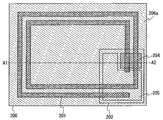
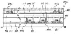
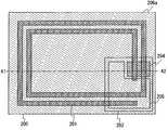
도 1a의 무선 칩(200)의 구조를 설명한다. 도 1b는 도 1a의 무선 칩(200)에서의 A1-A2 선을 따라 절취한 단면이다.The structure of the
도 1a 및 도 1b에 도시한 바와 같이, 본 실시 형태에서 나타내는 무선 칩(200)은 동일 기판(203) 위에 적층된 안테나(201)와 IC 칩(202)을 포함한다. 안테나(201)와 IC 칩(202)의 절연막을 개재해서 서로 적어도 일부 겹치도록 배치된다. IC 칩(202)은 용량 소자(220)를 구비하는 칩 내의 공진 용량 소자부(204)와, 전원 발생 수단, 제어 수단 및 메모리 수단 등을 포함하는 로직부(205)를 포함한다. 또한, 안테나(201)의 양단부는 로직부(205)의 집적 회로(207)와 전기적으로 접속된다. 또한, 도전성 차폐체(206a)는 보호막(213)과 충격 확산층(214a) 등의 절연막을 개재해서 안테나(201)에 겹치도록 배치되어, 도전성 차폐체(206a)가 무선 칩(200)의 최상부 표면 위에 구비된다.1A and 1B, the
본 실시 형태에서는 용량 소자(215a)가 안테나(201) 및 도전성 차폐체(206a)를 포함하고, 도전성 차폐체(206a)가 기판(203) 위에 구비되는 구성에 관해서 설명한다.A configuration in which the
집적 회로(207)는 불순물 영역을 각각 포함하는 반도체막(208a, 208b)과, 게이트 절연막(209)을 개재하여 반도체막(208a, 208b) 위에 구비된 게이트 전극(210)과, 게이트 전극(210)을 덮도록 구비된 제1 층간 절연막(211)과, 제1 층간 절연막(211) 위에 구비되고 또한, 반도체막(208a, 208b)의 불순물 영역과 전기적으로 접속하는 소스 및 드레인 전극(212)을 적어도 포함한다.The
또한, 집적 회로(207)에 접속되는 안테나(201)는 제2 층간 절연막(216)을 개재하여 배치된다. 도전성 차폐체(206a)는 보호막(213)과 충격 확산층(214a)을 사이에 두고 안테나(201) 위에 배치된다. 또한, 도전성 차폐체(206a)는 안테나(201)에 물리적으로 접속되지 않는다.Further, the
상기 구성에 의해, 도전성 차폐체(206a)와 안테나(201)는, 보호막(213)과 충격 확산층(214a)을 사이에 두고 전극으로 기능하고, 용량 소자(215a)를 형성한다.The
이어서, 상기 구성의 제조 방법에 관해서 이하로 간단하게 설명한다.Next, a manufacturing method of the above-described configuration will be briefly described below.
우선, 기판(203)을 준비한다. 기판(203)으로서, 예를 들어 바륨 붕규산 유리나, 알루미노 붕규산 유리 등의 유리 기판, 석영 기판, 세라믹 기판 등을 사용할 수 있다. 이와 달리, 스테인리스 스틸을 포함하는 금속 기판 또는 반도체 기판의 표면에 절연막을 형성한 반도체 기판을 사용해도 좋다. 플라스틱 등의 가요성을 갖는 합성 수지로 이루어지는 기판은 일반적으로 상술한 기판과 비교해서 내열 온도가 낮지만, 제조 공정동안 처리 온도에 견딜 수 있는 것이라면 사용하는 것이 가능하다. 또한, 기판(203)의 표면을 CMP법 등의 연마에 의해 평탄화해 두어도 좋다.First, the
이어서, 기판(203) 위에 로직부(205)에 포함되는 집적 회로(207)를 형성한다. 집적 회로(207)는 적어도 반도체막(208a, 208b)과, 반도체막(208a, 208b) 위에 게이트 절연막(209)을 개재하여 구비된 게이트 전극(210)과, 게이트 전극(210)을 덮도록 구비된 제1 층간 절연막(211)과, 제1 층간 절연막(211) 위에 구비된 소스 및 드레인 전극(212)을 갖는다. 또한, 용량 소자(220)는 집적 회로(207)에 포함된 소자와 동일한 공정을 사용하고, 마찬가지 방식으로 형성할 수 있기 때문에, 여기에서는 설명을 생략한다.The
반도체막(208a, 208b)은 비정질 반도체, 비정질 상태와 결정 상태가 혼재한 반도체, 0.5nm 내지 20nm 크기의 결정립을 관찰할 수 있는 미세결정 반도체 및 결정성 반도체로부터 선택된 어느 상태를 가져도 좋다. 본 실시 형태에서는 비정질 반도체막을 형성하고, 가열 처리에 의해 결정화하여 반도체막(208a, 208b)을 얻는다. 가열 처리는 로, 레이저 조사, 레이저광 대신 램프로부터 발광된 광의 조사(램프 어닐) 또는 이들을 조합해서 행할 수 있다.The
이어서, 반도체막(208a, 208b)을 덮도록 게이트 절연막(209)을 형성한다. 게이트 절연막(209)에는 예를 들어 산화 규소, 질화 규소, 질화 산화 규소 등의 임의의 것을 사용해서 단층 구조 또는 적층 구조를 갖도록 형성할 수 있다. 성막은 플라즈마 CVD법, 스퍼터링법 등에 의해 행해질 수 있다.Next, a
계속해서, 각각의 반도체막(208a, 208b) 위에 게이트 절연막(209)을 개재하여 게이트 전극(210)을 형성한다. 게이트 전극(210)은 단층 구조로 형성해도 좋고, 복수의 금속막의 적층 구조로 형성해도 좋다. 게이트 전극(210)은 CVD법이나 스퍼터링법에 의해, 탄탈(Ta), 텅스텐(W), 티타늄(Ti), 몰리브덴(Mo), 알루미늄(Al), 구리(Cu), 크롬(Cr), 네오디뮴(Nd)으로부터 선택된 원소 또는 상기 원소를 주성분으로 하는 합금 재료 또는 화합물 재료를 이용하여 형성할 수 있다. 본 실시 형태에서는 제1 도전층과 제2 도전층을 이 순서대로 적층시키고, 각각 질화 탄탈 및 텅스텐(W)을 사용한다.Subsequently, the
이어서, 마스크로서 패터닝된 게이트 전극(210) 또는 레지스트를 사용하여, 반도체막(208a, 208b)에 n형 또는 p형의 도전성을 부여하는 불순물을 선택적으로 첨가한다. 각각의 반도체막(208a, 208b)은 채널 형성 영역 및 불순물 영역(소스 영역, 드레인 영역, LDD 영역을 포함함)을 갖고, 첨가되는 불순물 원소의 도전성에 의해 n 채널형 박막 트랜지스터(이하, "n 채널형 TFT"라고도 함) 또는 p 채널형 박막 트랜지스터(이하, "p 채널형 TFT"라고도 함)를 얻을 수 있다.Next, an impurity imparting n-type conductivity or p-type conductivity is selectively added to the
도 1b에서는, n 채널형 TFT는 게이트 전극(210)의 측면에 측벽을 갖는다. n 채널형 TFT의 반도체막(208b)에 n형의 도전성을 부여하는 불순물이 선택적으로 첨가되어 소스 영역, 드레인 영역 및 LDD 영역이 형성된다. 한편, p 채널형 TFT의 반도체막(208a)에 p형의 도전성을 부여하는 불순물이 선택적으로 첨가되어 소스 영역 및 드레인 영역이 형성된다. 본 실시 형태에서는 게이트 전극(210)의 측면에 측벽을 형성하고, n 채널형 TFT에 선택적으로 LDD 영역을 형성하지만, 본 발명의 실시 형태는 이 구조에 한정되지 않는다. p 채널형 TFT에 LDD 영역을 형성해도 좋고, p 채널형 TFT에 측벽을 설치하지 않아도 좋다. 이와 달리, n 채널형 TFT와 p 채널형 TFT를 상보적 방식으로 사용하는 CMOS 구조를 채용할 수도 있다.In Fig. 1B, the n-channel TFT has a side wall on the side surface of the
이어서, 게이트 전극(210)을 덮도록 제1 층간 절연막(211)을 형성한다. 제1 층간 절연막(211)은 산화 규소(SiOx), 질화 규소(SiNx), 산화 질화 규소(SiOxNy)(x>y), 질화 산화 규소(SiNxOy)(x>y) 등의 산소 또는 질소를 함유한 절연막의 단층 구조 또는 이들의 적층 구조를 갖도록 형성될 수 있다. 이와 달리, 에폭시 수지, 아크릴 수지, 페놀 수지, 노볼락 수지, 멜라민 수지, 우레탄 수지 또는 실리콘 수지 등의 수지 재료를 사용할 수 있다. 이와 달리, 벤조시클로부텐, 파릴렌, 불화 아릴렌 에테르 또는 폴리이미드 등의 유기 재료, 실록산계 중합체 등의 중합에 의해 얻어지는 화합물 재료, 수용성 단독중합체와 수용성 공중합체를 포함하는 조성물 재료 등을 사용해서 제1 층간 절연막(211)을 형성해도 좋다.Next, a first
그 후, 제1 층간 절연막(211) 위에 소스 및 드레인 전극(212)을 형성한다. 소스 및 드레인 전극(212)은 반도체막(208a, 208b)의 불순물 영역과 전기적으로 접속한다. 도 1b에서는 소스 및 드레인 전극(212)과 같은 재료를 사용해서 배선을 형성한다. 소스 및 드레인 전극(212), 배선으로는 CVD법이나 스퍼터링법 등에 의해, 알루미늄(Al), 텅스텐(W), 티타늄(Ti), 탄탈(Ta), 몰리브덴(Mo), 니켈(Ni), 백금(Pt), 구리(Cu), 금(Au), 은(Ag), 망간(Mn), 네오디뮴(Nd), 탄소(C), 실리콘(Si)로부터 선택된 원소 또는 이들 원소를 주성분으로 하는 합금 재료 또는 화합물 재료를 사용하여, 단층 구조 또는 적층 구조를 갖도록 형성된다. 알루미늄을 주성분으로 하는 합금 재료는 예를 들어, 알루미늄을 주성분으로 한 니켈을 포함하는 재료 또는 알루미늄을 주성분으로 하고 니켈과, 탄소와 규소 중 한쪽 또는 양쪽을 포함하는 합금 재료이다. 소스 및 드레인 전극(212), 및 배선은 예를 들어, 배리어막과, 알루미늄 실리콘(Al-Si)막과 배리어막의 적층 구조, 배리어막과, 알루미늄 실리콘(Al-Si)막과 질화티타늄 막과, 배리어막의 적층 구조를 갖도록 형성될 수 있다. 또한, 배리어막은 티타늄, 티타늄의 질화물, 몰리브덴 또는 몰리브덴의 질화물로 이루어지는 박막이다. 알루미늄 및 알루미늄 실리콘은 저항값이 낮고 저렴하기 때문에, 소스 및 드레인 전극(212), 배선을 형성하는 재료로서 적절하다. 상층과 하층용으로 배리어막을 형성하면, 알루미늄 및 알루미늄 실리콘의 힐록 발생(hillock formation)을 방지할 수 있다. 환원성이 높은 원소인 티타늄으로 배리어막을 형성하면, 반도체막(208a, 208b) 위에 얇은 자연 산화막이 형성될 때에도, 이 자연 산화막을 환원하여, 반도체막(208a, 208b)과의 접촉을 향상시킬 수 있다.Thereafter, source and drain
계속해서, 소스 및 드레인 전극(212) 및 배선을 덮도록 제2 층간 절연막(216)을 형성한다. 제2 층간 절연막(216)은 상기 제1 층간 절연막(211)용의 재료 중 어느 하나를 사용해서 형성할 수 있다.Subsequently, a second
그 후, 제2 층간 절연막(216) 위에 안테나(201)를 형성하고, 안테나(201)위에 보호막(213)을 형성하고, 보호막(213) 위에 충격 확산층(214a)을 형성하고, 충격 확산층(214a) 위에 도전성 차폐체(206a)를 형성함으로써, 무선 칩(200)이 완성된다. 안테나(201)는 CVD법, 스퍼터링법, 스크린 인쇄법 또는 액적 토출법 등에 의해 도전성 재료를 사용해서 단층 구조 또는 적층 구조를 갖도록 형성된다. 도전성 재료는 알루미늄(Al), 티타늄(Ti), 은(Ag), 구리(Cu), 금(Au), 니켈(Ni)로 선택된 원소 또는 이들 원소를 주성분으로 하는 합금 재료 또는 화합물 재료로부터 선택된 원소이다. 보호막(213)은 상기 제1 층간 절연막(211)용 재료 중 임의의 재료를 사용해서 형성할 수 있다. 또한, 도 1a 및 도 1b에서는 2번 권취된 코일 안테나(201)를 용량 소자(215a)의 한쪽의 전극으로 사용했지만, 본 발명의 실시 형태는 이것에 한정되지 않고, 1번 또는 복수회 권취된 안테나를 용량 소자(215a)의 한쪽의 전극으로서 사용해도 좋다. 또한, 충격 확산층(214a)은 예를 들어, 섬유체에 유기 수지를 함침시킨 구조체 등을 사용할 수 있다. 이 경우, 보호막(213)에 충격 확산층(214a)을 접착시켜도 좋다. 또한, 도전성 차폐체(206a)는 스퍼터링법, 플라즈마 CVD법 또는 증착법 등의 건식법과, 도포법, 인쇄법, 액적 토출법(잉크젯법) 등의 습식법에 의해 형성할 수 있다.Thereafter, an
또한, 본 실시 형태에서는 용량 소자(215a)의 2개의 전극 중 한쪽은 안테나(201)이고, 다른 쪽은 도전성 차폐체(206a)이며, 안테나(201)와 도전성 차폐체(206a) 사이에 보호막(213)과 충격 확산층(214a)을 설치한 경우를 나타냈지만, 본 실시 형태는 이것에 한정되지 않는다. 전극 사이에 보호막(213)만을 설치하는 구성이어도 좋고, 충격 확산층(214a)만을 설치하는 구성이어도 좋다. 또한, 여기서 설명한 보호막과 충격 확산층 이외에 절연막을 배치해도 좋다. 즉, 용량 소자를 형성할 수 있으면, 본 실시 형태에서 설명한 구성 이외의 임의의 다른 구조를 채용할 수 있다.In this embodiment, one of the two electrodes of the
상기 구성으로, 도전성 차폐체(206a)와 안테나(201) 사이에 용량 소자(215a)가 형성되고, 도전성 차폐체(206a)를 배치하지 않는 경우와 비교해서, 칩 내에 형성되는 공진 용량 소자부(204)의 용량 소자(220)에서의 용량 소자의 수를 감소시킬 수 있다. 이에 따라, 무선 칩(200)의 크기와 IC 칩(202)의 크기를 축소할 수 있고, IC 칩 및 무선 칩 내의 한정된 면적을 효과적으로 활용할 수 있다. 또한, IC 칩 및 무선 칩의 크기를 축소할 수 있기 때문에, 소비 전류를 저감할 수 있고, 따라서 통신 거리의 저하를 방지할 수 있다. 또한, 도전성 차폐체(206a)를 사용함으로써, 정전기에 대한 내성 및 무선 칩이 소형화될 때 현저한 문제가 되는 무선 칩의 물리적 강도를 강화할 수 있다.The resonance
(실시 형태 2)(Embodiment 2)
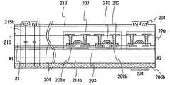
본 실시 형태에서는, 상기 실시 형태와는 다른 구조를 갖는 무선 칩(200)이 도면을 참조하여 설명한다. 구체적으로는, 용량 소자(215b)의 2개의 전극 중 하나로서 안테나(201)가 구비되고, 다른 쪽의 전극으로서 도전성 차폐체(206b)를 기판(203)의 아래에 배치하는 구성에 관해서 설명한다.In the present embodiment, a
도 2a의 무선 칩(200)의 구성을 나타낸다. 도 2b는 도 2a의 무선 칩(200)의 A1-A2 선을 따라 절취한 단면이다.2A shows a configuration of the
도 2a 및 도 2b는 용량 소자(215b)의 2개의 전극 중 안테나(201)를 한쪽의 전극으로서 설치하고, 다른 쪽의 전극으로서 도전성 차폐체(206b)를 기판(203) 아래에 배치하는 구성을 도시한다. 본 실시 형태에서 설명하는 무선 칩(200)은 동일 기판(203) 위에 적층된 안테나(201)와 IC 칩(202)을 포함하고, 안테나(201)와 IC 칩(202)은 절연막을 개재해서 서로 적어도 일부 겹치도록 배치한다. IC 칩(202)은 용량 소자(220)를 구비하는 칩 내의 공진 용량 소자부(204)와, 전원 발생 수단, 제어 수단 및 메모리 수단 등을 포함하는 로직부(205)를 갖고 있다. 또한, 안테나(201)의 양단부는 로직부(205)의 집적 회로(207)와 전기적으로 접속된다. 또한, 안테나(201)와 도전성 차폐체(206b)는 기판(203), 제1 층간 절연막(211), 제2 층간 절연막(216), 보호막(213), 충격 확산층(214b) 등을 개재하여 배치한다. 또한, 도전성 차폐체(206b)는 무선 칩(200)의 최하층에 설치한다.2A and 2B show a configuration in which the
또한, 집적 회로(207)에 접속되는 안테나(201)는 상기 실시 형태와 마찬가지로, 제2 층간 절연막(216)을 개재하여 배치된다. 본 실시 형태에서는 기판(203) 밑에 충격 확산층(214b)을 형성하고, 충격 확산층(214b) 아래에 도전성 차폐체(206b)를 형성한다. 도전성 차폐체(206b)는 안테나(201)에 물리적으로 접속되지 않는다.The
본 실시 형태에서는 도전성 차폐체(206b)와 안테나(201)가 기판(203), 제1 층간 절연막(211), 제2 층간 절연막(216), 충격 확산층(214b)을 개재하여 전극으로 기능하고, 용량 소자(215b)를 형성한다.The
또한, 본 실시 형태에서는 용량 소자(215b)의 2개의 전극의 한쪽이 안테나(201)이며, 다른 쪽이 도전성 차폐체(206b)이고, 안테나(201)와 도전성 차폐체(206b) 사이에 기판(203), 제1 층간 절연막(211), 제2 층간 절연막(216), 보호막(213), 충격 확산층(214b) 등을 설치한 경우를 설명했지만, 본 발명의 실시 형태는 이것에 한정되는 않는다. 용량 소자를 형성할 수 있으면, 본 실시 형태에서 설명한 구성 이외의 임의의 다른 구성을 형성할 수 있다.In this embodiment, one of the two electrodes of the
상기 구성으로, 도전성 차폐체(206b)와 안테나(201) 사이에 용량 소자(215b)가 형성되고, 도전성 차폐체(206b)를 배치하지 않는 경우와 비교해서, 칩 내에 형성되는 것이 요구되는 공진 용량 소자부(204)의 용량 소자(220)의 용량 소자 수를 감소시킬 수 있다. 이에 따라, 무선 칩(200)의 크기와 IC 칩(202)의 크기를 축소 할 수 있고, IC 칩 및 무선 칩 내의 한정된 면적을 효과적으로 활용할 수 있다. 또한, IC 칩 및 무선 칩의 크기를 축소할 수 있기 때문에, 소비 전류를 저감할 수 있고, 이에 따라 통신 거리의 저하를 방지할 수 있다. 또한, 도전성 차폐체(206b)를 사용함으로써, 정전기에 대한 내성 및 무선 칩이 소형화될 때 현저한 문제가 되는 무선 칩의 물리적 강도를 강화할 수 있다. 또한, 도전성 차폐체(206b)를 안테나 위에 설치하고 있지 않기 때문에, 실시 형태 1에서 설명한 구성과 비교해서 R/W로부터 전송되는 반송파 또는 진폭 변조파의 수신을 방해하지 않고, 양호한 통신 정밀도를 확보할 수 있다.In the above configuration, as compared with the case where the
(실시 형태 3)(Embodiment 3)
본 실시 형태에서는, 상기 실시 형태 1 및 2와는 다른 구성을 갖는 무선 칩(200)이 도면을 사용해서 설명된다. 구체적으로는, 무선 칩(200)은 용량 소자(215a)와 용량 소자(215c)를 갖는다. 용량 소자(215a)는 실시 형태 1과 마찬가지의 구성을 갖고, 안테나(201)와 보호막(213)과 충격 확산층(214a)과 도전성 차폐체(206a)의 적층 구조를 갖도록 형성된다. 또한, 용량 소자(215c)를 형성하는 2개의 전극 중 안테나(201)를 한쪽의 전극으로서 설치하고, 다른 쪽의 전극으로서 기판(203) 위에 설치한 도전성 차폐체(206a) 및 기판(203) 아래에 설치한 도전성 차폐체(206b)의 양쪽을 배치하는 구성에 관해서 설명한다.In this embodiment, a
도 3a의 무선 칩(200)의 구성을 나타낸다. 도 3b는 도 3a의 무선 칩(200)의 A1-A2 선을 따라 절취한 단면이다.3A shows the configuration of the
도 3a 및 도 3b는 용량 소자(215a)와 용량 소자(215c)를 갖는 구성을 도시한다. 용량 소자(215a)는 실시 형태 1과 같은 구성이기 때문에, 여기서는 설명을 생략한다. 용량 소자(215c)의 2개의 전극 중 안테나(201)를 한쪽의 전극으로서 설치하고, 기판(203) 위에 설치하는 도전성 차폐체(206a) 및 기판(203) 아래에 설치하는 도전성 차폐체(206b) 양쪽을 다른 쪽의 전극으로서 배치하는 구성이 설명된다. 본 실시 형태에서 설명하는 무선 칩(200)은 동일 기판(203) 위에 적층된 안테나(201)와 IC 칩(202)을 포함한다. 안테나(201)와 IC 칩(202)은 절연막을 개재해서 적어도 일부 겹쳐지도록 배치한다. IC 칩(202)은 용량 소자(220)를 구비하는 칩 내의 공진 용량 소자부(204)와, 전원 발생 수단, 제어 수단 및 메모리 수단 등을 포함하는 로직부(205)를 갖고 있다. 또한, 안테나(201)의 양단부는 로직부(205)의 집적 회로(207)에 전기적으로 접속된다. 또한, 안테나(201)와 도전성 차폐체(206a)는 보호막(213)과 충격 확산층(214a) 등의 절연막을 개재하여 배치해서 무선 칩(200)의 최상부 표면에 구비된다. 또한, 안테나(201)와 도전성 차폐체(206b)는 기판(203), 제1 층간 절연막(211), 제2 층간 절연막(216), 보호막(213) 및 충격 확산층(214b) 등을 개재해서 설치한다. 또한, 도전성 차폐체(206b)는 무선 칩(200)의 최하층에 설치한다.3A and 3B show a configuration having a
또한, 집적 회로(207)에 접속되는 안테나(201)는 제2 층간 절연막(216)을 개재하여 배치된다. 도전성 차폐체(206a) 및 도전성 차폐체(206b)는 안테나(201)에 물리적으로 접속되지 않는다.Further, the
본 실시 형태에서는 기판 상면에 배치한 도전성 차폐체(206a)와 안테나(201)가 보호막(213), 충격 확산층(214a)을 개재하여 전극으로 기능하여, 공진 용량 소자를 형성한다. 또한, 기판 하면에 배치한 도전성 차폐체(206b)와 안테나(201)가 기판, 제1 층간 절연막(211), 제2 층간 절연막(216), 충격 확산층(214b)을 개재하여 전극으로 기능하여, 공진 용량 소자를 형성한다. 즉, 용량 소자(215c)는 도전성 차폐체(206a)와 안테나(201) 사이에서 형성된 공진 용량 소자와, 도전성 차폐체(206b)와 안테나(201)의 사이에서 형성된 공진 용량 소자를 포함한다.In the present embodiment, the
따라서, 본 실시 형태에서 상술한 실시 형태보다도 많은 공진 용량 소자가 형성되기 때문에, 상술한 실시 형태보다도 칩 내의 공진 용량 소자부(204)의 용량 소자(220)의 용량 소자 수를 감소시킬 수 있다. 또한, 도전성 차폐체(206a)와 도전성 차폐체(206b) 사이에 IC 칩(202)을 개재하기 때문에, 상기 실시 형태보다도 또한, 무선 칩의 물리적 강도를 강화할 수 있다.Therefore, the number of capacitive elements of the
또한, 본 실시 형태에서 설명한 구성이 반드시 채용되지는 않는다. 용량 소자를 형성할 수 있으면, 보호막과 충격 확산층 이외에 절연층을 배치해도 좋고, 보호막과 충격 확산층을 배치하지 않아도 좋다.The configuration described in this embodiment is not necessarily employed. If a capacitive element can be formed, an insulating layer may be disposed in addition to the protective film and the shock-diffusing layer, or the protective film and the shock-diffusing layer may not be disposed.
(실시 형태 4)(Fourth Embodiment)
본 실시 형태에서는 상기 실시 형태와는 다른 구성을 갖는 무선 칩(200)이 도면을 사용해서 설명된다. 구체적으로는 용량 소자(215d, 215f)의 2개의 전극 중, 안테나(201)를 한쪽의 전극으로서 설치하고, 도전성 차폐체(206c)를 다른 쪽의 전극으로서 설치하여 무선 칩(200)에 포함된 다른 요소를 둘러싸도록 하는 구성에 관해서 설명한다.In the present embodiment, a
도 4a의 무선 칩(200)의 구성을 설명한다. 도 4b는 도 4a의 무선 칩(200)의 A1-A2 선을 따라 절취한 단면이다.The configuration of the
도 4a 및 도 4b는 각각의 용량 소자(215d, 215f)의 2개의 전극 중 안테나(201)를 한쪽의 전극으로서 설치하고, 다른 쪽의 전극으로서 구비된 도전성 차폐체(206c)를 배치하여 무선 칩(200)에 포함된 다른 요소를 둘러싸도록 하는 구성에 관해서 도시한다. 본 실시 형태에서 설명된 무선 칩(200)은 동일 기판(203) 위에 적층된 안테나(201)와 IC 칩(202)을 포함한다. 안테나(201)와 IC 칩(202)은 절연막을 개재해서 서로 적어도 일부 겹치도록 배치한다. IC 칩(202)은 용량 소자(220)를 구비하는 칩 내의 공진 용량 소자부(204)와, 전원 발생 수단, 제어 수단 및 메모리 수단 등을 포함하는 로직부(205)를 갖고 있다. 또한, 안테나(201)의 양단부는 로직부(205)의 집적 회로(207)에 전기적으로 접속된다. 또한, 안테나(201)와 도전성 차폐체(206c)는 보호막(213)이나 충격 확산층(214a, 214b) 등의 절연막을 개재해서 배치한다. 또한, 도전성 차폐체(206c)는 무선 칩(200)의 최외주 주위에 설치한다.4A and 4B show a case where the
또한, 집적 회로(207)에 접속되는 안테나(201)는 제2 층간 절연막(216)을 개재하여 배치된다. 도전성 차폐체(206c)는 안테나(201)에 물리적으로 접속되지 않는다.Further, the
상기 구성에서는 안테나(201)를 둘러싼 도전성 차폐체(206c)를 사용하여 공진 용량 소자가 형성되기 때문에, 본 실시 형태에서 형성되는 용량 소자(215d)를 정확하게 도시하는 것은 매우 곤란하다. 도 4에는 예를 들어 공진 용량 소자가 형성되는 개소에 용량 소자(215d)를 도시했다.In the above configuration, since the resonance capacitor element is formed using the
또한, IC 칩의 둘레에 도전성 차폐체(206c)를 설치하고 안테나(201)와 도전성 차폐체(206c)를 사용하여 용량 소자(215d, 215f)를 형성할 수 있는 구성이면, 본 실시 형태에 개시한 구성에 한정되지 않는다.If the
상기 구성으로, 상술한 실시 형태와 비교해서, 많은 공진 용량 소자를 형성할 수 있다. 또한, 임의의 상술한 실시 형태를 본 실시 형태와 조합함으로써, 물리적 강도를 향상시킬 수 있다.With the above configuration, a large number of resonance capacitors can be formed as compared with the above-described embodiments. In addition, by combining any of the above-described embodiments with the present embodiment, the physical strength can be improved.
(실시 형태 5)(Embodiment 5)
본 실시 형태에서는 상기 실시 형태와는 다른 구성을 갖는 무선 칩(200)이 도면을 사용해서 설명된다. 구체적으로는, 안테나(201)와 도전성 차폐체(206a)를 전극으로 한 용량 소자(215a) 외에, 칩 내의 공진 용량 소자부(204)의 넓게 형성한 배선(217)과 도전성 차폐체(206a)를 전극으로 한 용량 소자(215e)를 설치하는 구성에 관해서 설명한다.In the present embodiment, a
도 5a의 무선 칩(200)의 구성을 도시한다. 도 5b는 도 5a의 무선 칩(200)의 A1-A2 선을 따라 절취한 단면이다.5A shows a configuration of the
도 5a 및 도 5b는 용량 소자(215e)의 2개의 용량 소자 중 한쪽이 전극으로서 안테나(201) 및 도전성 차폐체(206a)를 갖고, 다른 쪽이 전극으로서 칩 내의 공진 용량 소자부(204)의 넓게 형성한 배선(217) 및 도전성 차폐체(206a)를 갖는 구성에 관해서 도시한다. 또한, 배선(217)은 소스 및 드레인 전극(212)과 동일 층에서 동일한 공정을 통해 형성될 수 있기 때문에, 특별한 공정을 필요로 하지 않는다.5A and 5B show that one of the two capacitive elements of the
본 실시 형태에서 설명하는 무선 칩(200)은 동일 기판(203) 위에 적층된 안테나(201)와 IC 칩(202)을 포함한다. 안테나(201)와 IC 칩(202)은 절연막을 개재해서 적어도 일부 겹치도록 배치된다. IC 칩(202)은 칩 내의 공진 용량 소자부(204)와, 전원 발생 수단, 제어 수단 및 메모리 수단 등을 포함하는 로직부(205)를 갖고 있다. 또한, 안테나(201)의 양단부는 로직부(205)의 집적 회로(207)에 전기적으로 접속된다. 또한, 배선(217)과 도전성 차폐체(206a)는 보호막(213)과 충격 확산층(214a) 및 제2 층간 절연막(216) 등의 절연막을 개재해서 배치하고, 도전성 차폐체(206a)는 무선 칩(200)의 최상부 표면에 구비된다.The
또한, 집적 회로(207)에 접속되는 안테나(201)는 제2 층간 절연막(216)을 개재하여 배치되고, 도전성 차폐체(206a)는 보호막(213)과 충격 확산층(214a)을 개재하여 안테나(201) 위에 배치된다. 도전성 차폐체(206a)는 안테나(201)에 물리적으로 접속되지 않는다.The
본 실시 형태에서 형성되는 용량 소자(215e)는 실시 형태 1과 마찬가지로 안테나(201)와 도전성 차폐체(206a)를 전극으로 한 용량 소자를 포함하고, 배선(217)이 넓게 형성된 칩 내의 공진 용량 소자부(204)의 배선(217)과 도전성 차폐체(206a)를 전극으로 한 용량 소자를 포함한다.The
또한, 여기에서는 실시 형태 1과 마찬가지로 최상부 표면에 도전성 차폐체(206a)를 설치하는 구성을 나타냈지만, 본 실시 형태는 상기 실시 형태 2 내지 실시 형태 4의 임의의 구성과도 자유롭게 조합해서 실시하는 것이 가능하다. 또한, 용량 소자(215e)가 형성될 수 있으면, 본 실시 형태에서 설명한 구조에 한정되는 것이 아니다.Although the configuration in which the
상기 구성으로, 도전성 차폐체(206a)를 배치하지 않는 경우에 비하여 칩 내 용량 소자를 저감시킬 수 있어 무선 칩(200)의 크기 및 IC 칩(202)의 크기를 축소하고, IC 칩의 한정된 면적을 효과적으로 이용하고, 소비 전류를 저감하고, 통신 거리의 저하를 방지할 수 있다. 또한, 도전성 차폐체(206a)를 사용함으로써, 정전기에 대한 내성 및 무선 칩이 소형화될 때 현저한 문제가 되는 무선 칩의 물리적 강도도 강화시킬 수 있다.With the above configuration, the capacitance in the chip can be reduced as compared with the case where the
또한, 상술한 실시 형태 1 내지 실시 형태 4에 본 구성을 조합함으로써, 본 구성을 채용하지 않는 실시 형태 1 내지 실시형태4와 비교해서 보다 많은 용량 소자를 형성할 수 있다.In addition, by combining this structure with the above-described
(실시 형태 6)(Embodiment 6)
본 실시 형태에서는 반도체 장치를 신뢰성이 높고, 높은 수율을 갖게 제조하는 방법에 대해서 도 6a 내지 도 6d를 참조하여 설명한다. 또한, 상술한 실시 형태 1 내지 실시 형태 5에서 기판을 갖는 구성이 설명되었지만, 본 실시 형태에서는 기판을 박리한 반도체 장치의 제조 방법에 대해서 설명한다. 또한, 상기 실시 형태 1 내지 실시 형태 5는 본 실시 형태와 자유롭게 조합하는 것이 가능하다. 또한, 본 실시 형태에서는 반도체 장치의 일례로서 CMOS(complementary metal oxide semiconductor)에 관해서 설명한다.In this embodiment, a method of manufacturing a semiconductor device with high reliability and high yield will be described with reference to FIGS. 6A to 6D. In addition, although the structure having the substrate in the above-described first to fifth embodiments has been described, the manufacturing method of the semiconductor device in which the substrate is peeled off will be described in this embodiment. Further, the first to fifth embodiments can be freely combined with the present embodiment. In this embodiment, a CMOS (complementary metal oxide semiconductor) will be described as an example of a semiconductor device.
박리층(901)을 개재하여 기판(900) 위에 트랜지스터(902, 903), 용량 소자(904), 절연층(905)이 구비되어, 반도체 집적 회로(910)가 형성된다(도 6a 참조). 또한, 본 실시 형태에서는 IC 칩 내에 형성되는 공진 용량 소자를 사용한 용량 소자를 형성하기 때문에, 용량 소자(904)는 종래의 용량 소자와 비교해서 작게 할 수 있다.
트랜지스터(902, 903)는 박막 트랜지스터이며, 각각은 소스 및 드레인 영역, 저농도 불순물 영역, 채널 형성 영역, 게이트 절연층, 게이트 전극, 소스 및 드레인 전극으로서 기능하는 배선을 갖는다. 소스 및 드레인 영역은 소스 및 드레인 전극으로서 기능하는 배선과 접하고, 전기적으로 접속된다.Each of the
트랜지스터(902)는 n 채널형 트랜지스터이며, 소스 또는 드레인 영역 및 저농도 불순물 영역에는 n형 도전성을 부여하는 불순물 원소(예를 들어 인(P)이나 비소(As) 등)를 포함한다. 트랜지스터(903)는 p 채널형 트랜지스터이며, 소스 또는 드레인 영역 및 저농도 불순물 영역에는 p형 도전성을 부여하는 불순물 원소(예를 들어 붕소(B), 알루미늄(Al)이나 갈륨(Ga) 등)를 포함한다.The
용량 소자(904)는 트랜지스터(902, 903)와 같은 공정으로 형성되고, 한쪽의 전극은 반도체층, 다른 쪽의 전극은 게이트 전극으로 형성된다. 이 경우, 용량값을 효율적으로 확보하기 위해서, 게이트 전극층을 형성하기 전에, 용량 소자(904)에 포함된 반도체층에 불순물 원소를 첨가해 두어도 좋다. 이 공정을 통해, 게이트 전극층의 하층 영역에 배치된 반도체층에도 불순물 원소가 첨가되고, 이에 따라 용량 소자(904)가 효율적으로 용량 소자로서 기능할 수 있다.The
이어서, 도전막을 사용하여 절연층(905) 위에 안테나(911)가 형성되고, 안테나(911) 위에 보호막(912)을 형성한다. 안테나(911)는 반도체 집적 회로에 전기적으로 접속된다. 도 6a에서, 안테나(911)는 용량 소자(904)의 한쪽의 전극에 전기적으로 접속된다.Subsequently, an
계속해서, 보호막(912) 위에 충격 확산층(920)을 형성한다. 충격 확산층(920)으로서, 예를 들어 섬유체(921)에 유기 수지(922)를 함침시킨 구조체가 사용될 수 있다.Subsequently, an
보호막(912)과 충격 확산층(920)을 함께 접착한 후, 계면으로서 박리층(901)을 따라 반도체 집적 회로(910), 안테나(911) 및 보호막(912)이 기판(900)으로부터 분리된다. 따라서, 반도체 집적 회로(910), 안테나(911) 및 보호막(912)은 충격 확산층(920)측에 구비된다(도 6b 참조).The semiconductor integrated
구체적으로 도시하지는 않았지만, 보호막(912)과 충격 확산층(920)의 접착에 대해서는 접착제, 압착 접합 또는 가열 압착 접착을 사용하여 행해질 수 있다.Although not specifically shown, adhesion between the
그 후, 박리층(901)을 개재하여 반도체 집적 회로(910)의 노출 박리면에 충격 확산층(930)을 접착하여, 반도체 집적 회로(910), 안테나(911) 및 보호막(912)을 충격 확산층(920)과 충격 확산층(930) 사이에 끼움 지지한다(도 6c 참조).Thereafter, the
충격 확산층(930)으로서, 충격 확산층(920)의 경우와 마찬가지로, 예를 들어 섬유체(931)에 유기 수지(932)를 함침시킨 구조체를 사용해도 좋다.A structure obtained by impregnating the
구체적으로 도시하고 있지 않지만, 충격 확산층(920) 및 충격 확산층(930)은 평면 방향으로 배열되도록 반도체 집적 회로(910), 안테나(911), 보호막(912)을 포함하는 복수의 구조체를 끼움 지지한다. 분단함으로써, 반도체 집적 회로(910), 안테나(911) 및 보호막(912)이 충격 확산층(920)과 충격 확산층(930) 사이에 끼움 지지된 구조를 각각 갖는 개별적인 반도체 집적 회로 칩을 제조한다. 분단의 수단으로서는 물리적으로 분단할 수 있으면 특별히 한정되지 않지만, 바람직한 일례로서, 본 실시 형태에서는 분단 선을 따라 레이저광을 조사함으로써 분단한다.Although not specifically shown, the shock-absorbing
레이저광을 조사해서 분단함으로써, 반도체 집적 회로 칩의 분단면(941, 942)에서 충격 확산층(920) 및 충격 확산층(930)이 용융하여, 함께 융착된다. 이에 따라, 개개의 반도체 집적 회로 칩은 반도체 집적 회로(910), 안테나(911) 및 보호막(912)이 충격 확산층(920) 및 충격 확산층(930)과 전체적으로 밀봉되는 구조를 갖는다(도 6d 참조).By irradiating the laser light and cutting it, the
여기에서는 구체적으로 도시하지 않지만, 반도체 집적 회로(910), 안테나(911) 및 보호막(912)의 전체면을 보다 양호하게 덮기 위해서, 충격 확산층(920) 및 충격 확산층(930)보다 외측 또는 내측에 절연체를 더 설치해도 좋다.Although not shown in detail here, in order to better cover the entire surface of the semiconductor integrated
마지막으로, 도 7a에 도시한 바와 같이 도전성 차폐체(1101)를 설치해서, 본 실시 형태의 반도체 장치가 완성된다. 또한, 도 7a에서는 실시 형태 4에서 설명한 구성과 마찬가지로 외측 전체를 덮도록 도전성 차폐체(1101)를 형성한 것을 예시하고 있지만, 임의의 다른 실시 형태로서 예시한 구조를 채용할 수 있다. 또한, 도 7a에서는 도전성 차폐체(1101)는 반도체 집적 회로 칩의 상면, 하면, 측면을 덮도록 형성된다. 도전성 차폐체(1101)는 상면 및 측면의 일부에 도전성 차폐체를 형성한 후, 반도체 집적 회로를 뒤집어서 하면 및 측면의 일부에 도전성 차폐체를 형성함으로써, 전체면을 덮도록 형성하면 좋다.Finally, as shown in Fig. 7A, the
도전성 차폐체(1101)는 R/W로부터 전송되는 반송파 또는 진폭 변조파의 수신을 최대한 방해하지 않는 정도로 충분히 작은 막 두께로 형성하면 좋다.The
또한, 도 7b에 도시한 바와 같이, 도전성 차폐체(1102)를 충격 확산층보다 내측에 설치하여, 반도체 집적 회로의 전체면을 덮도록 형성해도 좋다. 이렇게 반도체 집적 회로의 전체면을 덮도록 도전성 차폐체(1102)를 형성하기 위해서는 반도체 집적 회로를 충격 확산층들 사이에서 끼움 지지하여 접착하기 전에, 분단에 의해 개개의 반도체 집적 회로 칩을 형성할 필요가 있지만, 반드시 이 형태가 채용되는 것은 아니다. 예를 들어, 반도체 집적 회로 칩을 충격 확산층에서 끼움 지지하여 접착하기 전에, 반도체 집적 회로의 상면 및 하면에 도전성 차폐체를 형성해 두고, 충격 확산층에서 끼움 지지하여 접착한 후, 레이저광을 조사해서 분단하면, 분단면에서 도전성 차폐체가 용융하고, 반도체 집적 회로의 측면을 상하로부터 용착해서 덮는 방법이 채용될 수 있다.Alternatively, as shown in Fig. 7B, the
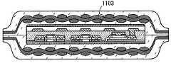
도 7c는 도전성 차폐체(1103)가 충격 확산층의 내측에 구비되어, 반도체 집적 회로의 한쪽 면에 형성한 예이다. 본 예에서는 실시 형태 1과 마찬가지로 도전성 차폐체(1103)가 안테나측에 형성되어 있으나, 도전성 차폐체(1103)는 실시 형태 2와 같이 박리면측에 형성해도 좋다.7C shows an example in which the
도전성 차폐체를 반도체 집적 회로의 한쪽 면에 형성함으로써, 도전성 차폐체가 R/W로부터 전송되는 반송파 또는 진폭 변조파의 수신을 방해하지 않아, 양호한 통신 정밀도를 확보할 수 있다.By forming the conductive shield on one surface of the semiconductor integrated circuit, the conductive shield does not interfere with the reception of the carrier wave or the amplitude-modulated wave transmitted from the R / W, thereby ensuring good communication accuracy.
이러한 형성 방법에 의해, 반도체 집적 회로를 개재해서 충격 확산층을 설치하고 있기 때문에, 제조 공정에서도 외부 스트레스나 응력에 의한 반도체 집적 회로의 파손이나 특성 불량 등의 악영향을 방지할 수 있다. 따라서 신뢰성을 높고, 수율이 높은 반도체 장치를 제조할 수 있다.According to such a forming method, since the impact diffusion layer is provided via the semiconductor integrated circuit, adverse effects such as breakage of the semiconductor integrated circuit due to external stress or stress and defective characteristics can be prevented in the manufacturing process. Therefore, a semiconductor device with high reliability and high yield can be manufactured.
또한, 본 실시 형태에 따라 제조한 반도체 장치는 가요성의 충격 확산층을 사용함으로써, 가요성이 있을 수 있다.Further, the semiconductor device manufactured according to the present embodiment may be flexible by using a flexible shock-absorbing layer.
트랜지스터(902, 903) 및 용량 소자(904)에 포함된 반도체층은 다음의 물질 중 임의의 물질 즉, 실란이나 게르만으로 대표되는 반도체 재료 가스를 사용해서 기상 성장법이나 스퍼터링법에 의해 제조되는 비정질 반도체, 비정질 반도체를 광 에너지나 열 에너지를 이용해서 결정화시켜 형성된 다결정 반도체, 또는 미세결정(세미 아몰퍼스라도도 함) 반도체를 사용해서 형성될 수 있다. 반도체층은 스퍼터링법, LPCVD법 또는 플라즈마 CVD법 등에 의해 형성될 수 있다.The semiconductor layers included in the
미세결정 반도체막은 깁스(Gibbs) 자유에너지를 고려하면 비정질과 단결정의 중간적인 준안정 상태에 속하는 것이다. 즉, 미세결정 반도체막은 자유 에너지면에서 안정된 제3 상태를 갖는 반도체이며, 단거리 질서(short range order)를 갖고 격자 왜곡을 갖는다. 기둥 형상 또는 바늘 형상 결정이 기판 표면에 대하여 법선 방향으로 성장한다. 미세결정 반도체의 대표예인 미세결정 실리콘의 라만 스펙트럼은 단결정 실리콘의 라만 스펙트럼의 피크를 나타내는 520cm-1보다도 낮은 파수로 시프트한다. 즉, 단결정 실리콘을 나타내는 520cm-1과 아몰퍼스 실리콘을 나타내는 480cm-1 사이에 미세결정 실리콘의 라만 스펙트럼의 피크가 있다. 또한, 미세결정 반도체막은 댕글링 결합(dangling bonds)을 종료시키기 위해 수소 또는 할로겐을 적어도 1 원자% 포함한다. 또한, 헬륨, 아르곤, 크립톤 또는 네온 등의 희가스(rare gas) 원소를 포함시켜서 격자 왜곡을 더 촉진시킴으로써, 안정성이 향상되고 양호한 미세결정 반도체막이 얻어질 수 있다.Considering the Gibbs free energy, the microcrystalline semiconductor film belongs to an intermediate metastable state between amorphous and single crystals. That is, the microcrystalline semiconductor film is a semiconductor having a third state that is stable in terms of free energy, has short-range order, and has lattice distortion. Columnar or needle-like crystals grow in the normal direction with respect to the substrate surface. The Raman spectrum of the microcrystalline silicon, which is a typical example of the microcrystalline semiconductor, shifts to a wave number lower than 520 cm-1 , which indicates the peak of the Raman spectrum of the single crystal silicon. In other words, the peak of the Raman spectrum of the microcrystalline silicon between 480cm-1 and 520cm-1 showing the amorphous silicon indicates a single crystalline silicon. In addition, the microcrystalline semiconductor film contains at least 1 atomic% of hydrogen or halogen to terminate the dangling bonds. Further, by including a rare gas element such as helium, argon, krypton, or neon to further promote lattice distortion, stability can be improved and a good microcrystalline semiconductor film can be obtained.
이 미세결정 반도체막은 주파수가 몇십 MHz 내지 몇백 MHz의 고주파 플라즈마 CVD법 또는 주파수가 1GHz 이상의 마이크로파 플라즈마 CVD 장치에 의해 형성될 수 있다. 미세결정 반도체막은 대표적으로는 SiH4, Si2H6, SiH2Cl2, SiHCl3, SiCl4, SiF4등의 수소화 규소를 수소로 희석해서 형성할 수 있다. 이와 달리, 수소화 규소 및 수소에 더하여, 헬륨, 아르곤, 크립톤, 네온으로부터 선택된 일종 또는 복수종의 희가스 원소로 희석해서 미세결정 반도체막을 형성할 수 있다. 이 경우, 수소화 규소에 대한 수소의 유량비를 5:1 내지 200:1, 바람직하게는 50:1 내지 150:1, 더욱 바람직하게는 100:1로 설정할 수 있다.This microcrystalline semiconductor film can be formed by a high frequency plasma CVD method with a frequency of several tens MHz to several hundred MHz or a microwave plasma CVD apparatus with a frequency of 1 GHz or more. Typically, the microcrystalline semiconductor film can be formed by diluting hydrogenated silicon such as SiH4 , Si2 H6 , SiH2 Cl2 , SiHCl3 , SiCl4 , and SiF4 with hydrogen. Alternatively, in addition to silicon hydride and hydrogen, a microcrystalline semiconductor film can be formed by diluting with one or more rare gas elements selected from helium, argon, krypton, and neon. In this case, the flow rate ratio of hydrogen to silicon hydride can be set to 5: 1 to 200: 1, preferably 50: 1 to 150: 1, more preferably 100: 1.
아몰퍼스 반도체로서는 대표적으로 수소화 아몰퍼스 실리콘, 결정성 반도체로서는 대표적으로 폴리 실리콘(다결정 실리콘) 등을 들 수 있다. 폴리 실리콘의 예로서는 800℃ 이상의 프로세스 온도에서 형성되는 폴리 실리콘을 주재료로서 사용한 소위 고온 폴리 실리콘과, 600℃ 이하의 프로세스 온도에서 형성되는 폴리 실리콘을 주재료로서 사용한 소위 저온 폴리 실리콘, 및 결정화를 촉진하는 원소 등을 사용하여 비정질 실리콘을 결정화시킨 폴리 실리콘 등이 포함된다. 물론, 전술한 바와 같이, 미세결정 반도체 또는 반도체층의 일부에 결정 상을 포함하는 반도체를 사용할 수도 있다.Representative examples of the amorphous semiconductor include hydrogenated amorphous silicon, and typical examples of the crystalline semiconductor include polysilicon (polycrystalline silicon). Examples of the polysilicon include so-called high-temperature polysilicon using polysilicon formed at a process temperature of 800 ° C or higher as a main material, so-called low-temperature polysilicon using polysilicon formed at a process temperature of 600 ° C or lower as a main material, And polysilicon in which amorphous silicon is crystallized by using the above-mentioned material. Of course, as described above, a semiconductor containing a crystal phase may be used for a part of the microcrystalline semiconductor or the semiconductor layer.
또한, 반도체의 재료로서는 실리콘(Si), 게르마늄(Ge) 등의 단체의 이외에 GaAs, InP, SiC, ZnSe, GaN, SiGe 등과 같은 화합물 반도체도 사용할 수 있다. 이와 달리, 산화물 반도체인 산화아연(ZnO), 산화주석(SnO2), 산화마그네슘 아연, 산화갈륨, 인듐 산화물 및 상기 산화물 반도체 중 임의로 구성되는 산화물 반도체 등을 사용할 수 있다. 예를 들어, ZnO, 인듐 산화물 및 산화갈륨으로 구성되는 산화물 반도체가 사용될 수 있다. 또한, ZnO를 반도체층에 사용하는 경우, 게이트 절연층은 Y2O3, Al2O3, TiO2, 및 이들 중 임의의 것의 적층 등을 사용하여 형성되는 것이 바람직하다. 게이트 전극층, 소스 전극층 및 드레인 전극층으로서는 인듐 주석 산화물(ITO), Au, Ti 등을 사용하면 좋다. 이와 달리, ZnO에 In이나 Ga 등을 첨가하여 사용할 수도 있다.As the material of the semiconductor, compound semiconductors such as GaAs, InP, SiC, ZnSe, GaN, SiGe and the like may be used in addition to the single body of silicon (Si) or germanium (Ge) Alternatively, oxide semiconductors arbitrarily composed of zinc oxide (ZnO), tin oxide (SnO2 ), zinc oxide, gallium oxide, indium oxide and the oxide semiconductor, which are oxide semiconductors, can be used. For example, an oxide semiconductor composed of ZnO, indium oxide, and gallium oxide may be used. When ZnO is used for the semiconductor layer, it is preferable that the gate insulating layer is formed by using Y2 O3 , Al2 O3 , TiO2 , or a lamination of any of them. As the gate electrode layer, the source electrode layer, and the drain electrode layer, indium tin oxide (ITO), Au, Ti, or the like may be used. Alternatively, In or Ga may be added to ZnO.
반도체층에 대해 결정성 반도체층을 사용하는 경우, 결정성 반도체층은 다양한 방법(레이저 결정화법, 열 결정화법 및 니켈 등의 결정화를 촉진하는 원소를 사용한 열 결정화법 등) 중 임의의 방법에 의해 형성될 수 있다. 또한, 미세결정 반도체를 레이저 조사해서 결정화하고, 결정성을 높일 수도 있다. 결정화를 촉진하는 원소를 도입하지 않는 경우에는, 비정질 규소막에 레이저광을 조사하기 전에, 질소 분위기에서 1시간동안 500℃의 온도로 비정질 규소막을 가열함으로써 비정질 규소막의 함유 수소 농도가 1× 10²⁰atoms/cm3 이하가 될까지 수소가 방출된다. 이것은 수소를 많이 포함한 비정질 규소막에 레이저광을 조사하면 비정질 규소막이 파괴되기 때문이다.When a crystalline semiconductor layer is used for the semiconductor layer, the crystalline semiconductor layer can be formed by any of various methods (laser crystallization method, thermal crystallization method, thermal crystallization method using an element promoting crystallization such as nickel, etc.) . Further, the microcrystalline semiconductor can be crystallized by laser irradiation to increase the crystallinity. Does not introduce an element for promoting crystallization, the amorphous before irradiation with a laser beam to the silicon film, the concentration of hydrogen-containing amorphous silicon film is 1 × 10²⁰ heated film amorphous silicon to a temperature of 500 ℃ for one hour in a nitrogen atmosphere atoms / cm <3 >. This is because the amorphous silicon film is destroyed when laser light is irradiated on the amorphous silicon film containing a large amount of hydrogen.
비정질 반도체층에 금속 원소의 도입 방법으로는 금속 원소를 비정질 반도체층의 표면 또는 그 내부에 도입할 수 있는 방법이면 특별히 한정되지 않는다. 예를 들어, 스퍼터링법, CVD법, 플라즈마 처리법(플라즈마 CVD법도 포함), 흡착법, 또는 금속염의 용액을 도포하는 방법을 사용할 수 있다. 이들 중 용액을 사용하는 방법은 간단해서, 금속 원소의 농도 조정이 용이하다고 하는 점에서 유용하다. 이때, 비정질 반도체층의 표면의 습윤성을 개선하여 비정질 반도체층의 표면 전체에 수용액이 확산되도록 위해, 산소 분위기에서의 UV 광의 조사, 열산화법, 히드록시 라디칼을 포함하는 오존수 또는 과산화수소에 의한 처리 등에 의해, 산화막을 형성하는 것이 바람직하다.The method of introducing the metal element into the amorphous semiconductor layer is not particularly limited as long as the method can introduce the metal element into the surface of the amorphous semiconductor layer or into the amorphous semiconductor layer. For example, a sputtering method, a CVD method, a plasma processing method (including a plasma CVD method), an adsorption method, or a method of applying a solution of a metal salt can be used. Of these, the method of using the solution is simple, and is useful in that it is easy to adjust the concentration of the metal element. At this time, in order to improve the wettability of the surface of the amorphous semiconductor layer and to diffuse the aqueous solution over the entire surface of the amorphous semiconductor layer, irradiation with UV light in an oxygen atmosphere, thermal oxidation, treatment with ozone water containing hydrogen radical or hydrogen peroxide , It is preferable to form an oxide film.
또한, 비정질 반도체층을 결정화하고, 결정성 반도체층을 형성하는 결정화 공정에서, 비정질 반도체층에 결정화를 촉진하는 원소(촉매 원소 또는 금속 원소라고도 함)를 첨가하고, 열처리(550℃ 내지 750℃에서 3분 내지 24시간)에 의해 결정화를 행해도 된다. 결정화를 촉진하는 원소로서는 철(Fe), 니켈(Ni), 코발트(Co), 루테늄(Ru), 로듐(Rh), 팔라듐(Pd), 오스뮴(Os), 이리듐(Ir), 백금(Pt), 구리(Cu) 및 금(Au)과 같은 하나 이상의 원소일 수 있다.Further, in the crystallization step of crystallizing the amorphous semiconductor layer and forming the crystalline semiconductor layer, an element for promoting crystallization (also referred to as a catalytic element or a metal element) is added to the amorphous semiconductor layer and heat treatment (at 550 캜 to 750 캜 3 minutes to 24 hours). Examples of the element that promotes crystallization include Fe, Ni, Co, Ru, Rh, Pd, Os, Ir, , Copper (Cu), and gold (Au).
결정화를 촉진하는 원소를 결정성 반도체층으로부터 제거 또는 경감하기 위해서, 불순물 원소를 포함하는 반도체층이 결정성 반도체층에 접하여 형성되고, 게터링 싱크로서 기능하게 된다. 불순물 원소로서는 n형을 부여하는 불순물 원소, p형을 부여하는 불순물 원소나 희가스 원소 등을 사용할 수 있고, 예를 들어 인(P), 질소(N), 비소(As), 안티몬(Sb), 비스무트(Bi), 붕소(B), 헬륨(He), 네온(Ne), 아르곤(Ar), Kr(크립톤), Xe(크세논) 중 하나 이상을 사용할 수 있다. 결정화를 촉진하는 원소를 포함하는 결정성 반도체층에, 희가스 원소를 포함하는 반도체층을 형성하고, 열처리(550℃ 내지 750℃에서 3분 내지 24시간)를 행한다. 결정성 반도체층에 포함되는 결정화를 촉진하는 원소는 희가스 원소를 포함하는 반도체층으로 이동하여, 결정성 반도체층에 포함된 결정화를 촉진하는 원소는 제거 또는 경감된다. 그 후, 게터링 싱크로서 기능하는 희가스 원소를 포함하는 반도체층을 제거한다.A semiconductor layer containing an impurity element is formed in contact with the crystalline semiconductor layer so as to function as a gettering sink in order to remove or reduce an element for promoting crystallization from the crystalline semiconductor layer. As the impurity element, for example, phosphorus (P), nitrogen (N), arsenic (As), antimony (Sb), and antimony can be used as the impurity element which imparts n type, impurity element which gives p type, At least one of Bi, Boron, He, Ne, Ar, Kr, and Xe can be used. A semiconductor layer containing a rare-gas element is formed on a crystalline semiconductor layer containing an element for promoting crystallization, and a heat treatment (550 to 750 ° C for 3 minutes to 24 hours) is performed. The element for promoting crystallization included in the crystalline semiconductor layer moves to the semiconductor layer containing the rare gas element and the element for promoting crystallization included in the crystalline semiconductor layer is removed or reduced. Thereafter, the semiconductor layer containing the rare-gas element serving as a gettering sink is removed.
비정질 반도체층은 열처리와 레이저광 조사의 조합에 의해 결정화되거나 또는 열처리와 레이저광 조사 중 하나가 복수회 행해질 수도 있다.The amorphous semiconductor layer may be crystallized by a combination of heat treatment and laser light irradiation, or one of heat treatment and laser light irradiation may be performed plural times.
결정성 반도체층을 직접 기판에 플라즈마법에 의해 형성해도 좋다. 이와 달리, 플라즈마법을 사용하여, 결정성 반도체층을 선택적으로 기판 위에 형성해도 좋다.The crystalline semiconductor layer may be directly formed on the substrate by a plasma method. Alternatively, the crystalline semiconductor layer may be selectively formed on the substrate using a plasma method.
게이트 절연층은 산화 규소를 사용해서 형성할 수 있고, 또는 산화 규소와 질화 규소를 포함하는 적층 구조를 갖도록 형성할 수도 있다. 게이트 절연층은 플라즈마 CVD법이나 감압 CVD법에 의해 절연막을 퇴적함으로써 형성해도 좋고, 플라즈마 처리에 의한 고상 산화 또는 고상 질화에 의해 형성해도 좋다. 이는, 단결정 반도체층을 플라즈마 처리에 의해 산화 또는 질화함으로써 형성하는 게이트 절연층이 치밀하고 절연 내압(withstand voltage)이 높고 신뢰성이 우수하기 때문이다. 예를 들어, 아산화질소(N2O)를 Ar로 1 내지 3배(유량비)만큼 희석하고, 10 내지 30Pa의 압력에서 3kW 내지 5kW의 마이크로파(2.45GHz) 전력을 인가해서 반도체층의 표면을 산화 또는 질화시킨다. 이 처리에 의해, 1nm 내지 10nm(바람직하게는 2nm 내지 6nm)의 두께를 가진 절연막을 형성한다. 또한, 아산화질소(N2O)와 실란(SiH4)을 도입하고, 10 내지 30Pa의 압력에서 3 내지 5kW의 마이크로파(2.45GHz) 전력을 인가해서 기상 성장법에 의해 산화 질화 규소막을 형성해서 게이트 절연층을 형성한다. 고상 반응과 기상 성장법에 의한 반응을 조합함으로써, 계면 준위 밀도가 낮고 절연 내압이 우수한 게이트 절연층을 형성할 수 있다.The gate insulating layer may be formed using silicon oxide, or may be formed to have a laminated structure including silicon oxide and silicon nitride. The gate insulating layer may be formed by depositing an insulating film by a plasma CVD method or a low pressure CVD method, or may be formed by solid-state oxidation or solid-state nitridation by plasma treatment. This is because the gate insulating layer formed by oxidizing or nitriding the single crystal semiconductor layer by the plasma treatment is dense, the withstand voltage is high, and the reliability is excellent. For example, nitrous oxide (N2 O) is diluted with Ar to 1 to 3 times (flow rate ratio) and microwave power of 3 kW to 5 kW (2.45 GHz) is applied at a pressure of 10 to 30 Pa to oxidize the surface of the semiconductor layer Or nitrided. By this treatment, an insulating film having a thickness of 1 nm to 10 nm (preferably 2 nm to 6 nm) is formed. Further, a silicon oxynitride film is formed by a vapor phase growth method by introducing nitrous oxide (N2 O) and silane (SiH4 ) and applying a microwave (2.45 GHz) power of 3 to 5 kW at a pressure of 10 to 30 Pa, Thereby forming an insulating layer. By combining the solid phase reaction and the reaction by the vapor phase growth method, a gate insulating layer having a low interfacial level density and excellent dielectric strength can be formed.
게이트 절연층으로서, 이산화 지르코늄, 산화 하프늄, 이산화 티타늄, 5산화탄탈 등의 고유전율 재료를 사용해도 좋다. 게이트 절연층용으로 고유전율 재료를 사용함으로써, 게이트 누설 전류를 저감할 수 있다.As the gate insulating layer, a high dielectric constant material such as zirconium dioxide, hafnium oxide, titanium dioxide, or tantalum pentoxide may be used. By using a high dielectric constant material for the gate insulating layer, the gate leakage current can be reduced.
게이트 전극층은 CVD법, 스퍼터링법, 액적 토출법등을 사용해서 형성할 수 있다. 게이트 전극층은 Ag, Au, Cu, Ni, Pt, Pd, Ir, Rh, W, Al, Ta, Mo, Cd, Zn, Fe, Ti, Si, Ge, Zr, Ba로부터 선택된 원소 또는 상기 원소들 어느 하나를 주성분으로 포함하는 합금 재료 또는 화합물 재료로 형성하면 좋다. 이와 달리, 인 등의 불순물 원소를 도핑한 다결정 규소막에 의해 대표되는 반도체막이나, AgPdCu 합금을 사용해도 좋다. 또한, 단층 구조 또는 복수층의 구조를 채용할 수 있고, 예를 들어, 질화 텅스텐 막과 몰리브덴 막의 2층 구조로 해도 좋고, 막 두께 50nm의 텅스텐 막, 막 두께 500nm의 알루미늄과 실리콘(Al-Si)의 합금막, 막 두께 30nm의 질화 티타늄 막을 순차 적층한 3층 구조로 해도 좋다. 또한, 3층 구조의 경우, 제1 도전막으로서 텅스텐 막 대신에 질화 텅스텐막을 사용해도 좋고, 제2 도전막으로서 알루미늄과 실리콘의 합금(Al-Si)막 대신에 알루미늄과 티타늄(Al-Ti)의 합금막을 사용해도 좋고, 제3 도전막으로서 질화티타늄 막 대신에 티타늄막을 사용해도 좋다.The gate electrode layer can be formed by using a CVD method, a sputtering method, a droplet discharge method, or the like. The gate electrode layer may be formed of an element selected from Ag, Au, Cu, Ni, Pt, Pd, Ir, Rh, W, Al, Ta, Mo, Cd, Zn, Fe, Ti, Si, Ge, Zr, It may be formed of an alloy material or a compound material containing one as a main component. Alternatively, a semiconductor film typified by a polycrystalline silicon film doped with an impurity element such as phosphorus or an AgPdCu alloy may be used. For example, a tungsten film having a thickness of 50 nm, aluminum having a thickness of 500 nm and silicon (Al-Si (Al-Si)) having a thickness of 500 nm may be used, ), And a titanium nitride film having a thickness of 30 nm are successively laminated on one another. In the case of the three-layer structure, a tungsten nitride film may be used instead of the tungsten film as the first conductive film, and aluminum and titanium (Al-Ti) may be used instead of the aluminum- Or a titanium film may be used instead of the titanium nitride film as the third conductive film.
게이트 전극층으로서, 가시광에 대하여 투광성을 갖는 투광성의 재료를 사용할 수도 있다. 투광성의 도전 재료로서는 인듐 주석 산화물(ITO), 산화 규소를 포함하는 인듐 주석 산화물(ITSO), 유기 인듐, 유기 주석, 산화 아연 등을 사용할 수 있다. 이와 달리, 산화 아연(ZnO)을 포함하는 인듐 아연 산화물(IZO), 산화 아연(ZnO),갈륨(Ga)을 도프한 ZnO, 산화 주석(SnO2), 산화 텅스텐을 포함하는 인듐 산화물, 산화 텅스텐을 포함하는 인듐 아연 산화물, 산화 티타늄을 포함하는 인듐 산화물, 산화 티타늄을 포함하는 인듐 주석 산화물 등도 사용해도 좋다.As the gate electrode layer, a light-transmitting material having a light-transmitting property with respect to visible light may be used. As the light-transmitting conductive material, indium tin oxide (ITO), indium tin oxide containing silicon oxide (ITSO), organic indium, organotin, zinc oxide and the like can be used. Alternatively, indium oxide including indium zinc oxide (IZO), zinc oxide (ZnO), gallium (Ga) -doped ZnO, tin oxide (SnO2 ), indium oxide including tungsten oxide, tungsten oxide Indium oxide containing titanium oxide, indium tin oxide containing titanium oxide, or the like may also be used.
게이트 전극층을 형성하는데 에칭 가공이 필요한 경우, 마스크를 형성하고, 건식 에칭 또는 습식 에칭을 행할 수 있다. ICP(inductively coupled plasma: 유도 결합형 플라즈마) 에칭법을 사용하고 에칭 조건(코일형의 전극에 인가되는 전력량, 기판측의 전극에 인가되는 전력량, 기판측의 전극 온도 등)을 적절히 조절함으로써, 전극층을 테이퍼 형상으로 에칭할 수 있다. 또한, 에칭용 가스로서는 Cl2, BCl3, SiCl4 또는 CCl4등을 대표로 하는 염소계 가스, CF4, SF6 또는 NF3등을 대표로 하는 불소계 가스 또는 O2를 적절히 사용할 수 있다.When an etching process is required to form the gate electrode layer, a mask can be formed, and dry etching or wet etching can be performed. (Inductively coupled plasma (ICP)) etching method and appropriately adjusting the etching conditions (the amount of power applied to the coil-shaped electrode, the amount of power applied to the electrode on the substrate side, the electrode temperature on the substrate side, and the like) Can be etched in a tapered shape. As the etching gas, Cl2 , BCl3 , SiCl4 or CCl4 Chlorine-based gas represented by CF4 , SF6 or NF3 Or fluorine-based gas represented by O2 or O2 can be suitably used.
본 실시 형태에서는 트랜지스터 구조로서 단일 게이트 구조를 설명했지만, 이와 달리 더블 게이트 구조 등의 멀티 게이트 구조를 채용할 수 있다. 이 경우, 반도체층의 위, 아래에 게이트 전극층을 설치할 수 있고, 또는 반도체층의 한쪽 측(위 또는 아래)에만 복수 게이트 전극층을 설치할 수도 있다.In the present embodiment, a single gate structure is described as a transistor structure, but a multi-gate structure such as a double gate structure can be adopted. In this case, a gate electrode layer may be provided above or below the semiconductor layer, or a plurality of gate electrode layers may be provided only on one side (upper or lower) of the semiconductor layer.
이와 달리, 트랜지스터의 소스 영역 및 드레인 영역 위에 실리사이드를 설치하여도 좋다. 실리사이드는 반도체층의 소스 영역 및 드레인 영역 위에 도전막을 형성하고, 가열 처리, GRTA법, LRTA법 등에 의해, 노출된 소스 및 드레인 영역의 반도체층의 규소와 도전막을 반응시켜서 형성한다. 이와 달리, 레이저 조사나 램프를 이용한 광 조사에 의해 실리사이드를 형성해도 좋다. 실리사이드를 형성하는 도전막의 재료로서는 티타늄(Ti), 니켈(Ni), 텅스텐(W), 몰리브덴(Mo), 코발트(Co), 지르코늄(Zr), 하프늄(Hf), 탄탈(Ta), 바나듐(V), 네오디뮴(Nd), 크롬(Cr), 백금(Pt), 팔라듐(Pd) 중 임의의 것이 사용될 수 있다.Alternatively, silicide may be provided on the source region and the drain region of the transistor. The silicide is formed by forming a conductive film on the source region and the drain region of the semiconductor layer and reacting the silicon of the semiconductor layer of the exposed source and drain regions with the conductive film by heat treatment, GRTA method, LRTA method or the like. Alternatively, the silicide may be formed by laser irradiation or light irradiation using a lamp. As a material of the conductive film for forming the silicide, a conductive material such as titanium (Ti), nickel (Ni), tungsten (W), molybdenum (Mo), cobalt (Co), zirconium (Zr), hafnium (Hf), tantalum V), neodymium (Nd), chromium (Cr), platinum (Pt), and palladium (Pd).
소스 전극층 또는 드레인 전극층으로서 기능하는 배선층은 PVD법, CVD법, 증착법 등에 의해 도전막을 성막한 후, 이 도전막을 원하는 형상으로 에칭해서 형성할 수 있다. 이와 달리, 인쇄법, 전해 도금법 등에 의해, 소정의 장소에 선택적으로 배선층을 형성할 수 있다. 이와 달리, 리플로우법 또는 다마신법을 사용해도 좋다. 배선층의 재료로서는 Ag, Au, Cu, Ni, Pt, Pd, Ir, Rh, W, Al, Ta, Mo, Cd, Zn, Fe, Ti, Zr 또는 Ba 등의 금속, Si 또는 Ge 등의 반도체 또는 그 합금, 또는 그 질화물을 사용해서 형성하면 좋다. 이와 달리, 투광성의 재료도 사용할 수 있다.The wiring layer serving as the source electrode layer or the drain electrode layer can be formed by forming a conductive film by a PVD method, a CVD method, a vapor deposition method, or the like, and then etching the conductive film into a desired shape. Alternatively, the wiring layer can be selectively formed at a predetermined place by a printing method, an electrolytic plating method, or the like. Alternatively, a reflow method or a damascene method may be used. As the material of the wiring layer, a metal such as Ag, Au, Cu, Ni, Pt, Pd, Ir, Rh, W, Al, Ta, Mo, Cd, Zn, Fe, Ti, Zr or Ba, The alloy, or the nitride thereof. Alternatively, a translucent material may be used.
또한, 투광성의 도전성 재료로서, 인듐 주석 산화물(ITO), 산화 규소를 포함하는 인듐 주석 산화물(ITSO), 산화 아연(ZnO)을 포함하는 인듐 아연 산화물(IZO), 산화 아연(ZnO), 갈륨(Ga)을 도프한 ZnO, 산화 주석(SnO2), 산화 텅스텐을 포함하는 인듐 산화물, 산화 텅스텐을 포함하는 인듐 아연 산화물, 산화 티타늄을 포함하는 인듐 산화물, 산화 티타늄을 포함하는 인듐 주석 산화물 등을 사용할 수 있다.As the transparent conductive material, indium tin oxide (ITO), indium tin oxide (ITSO) containing silicon oxide, indium zinc oxide (IZO), zinc oxide (ZnO), gallium Indium oxide containing tungsten oxide, indium zinc oxide containing tungsten oxide, indium oxide containing titanium oxide, indium tin oxide containing titanium oxide, or the like can be used, for example, ZnO, tin oxide (SnO2 ) doped with Ga .
도전성 차폐체를 형성하는 재료로서는 도전체 또는 반도체가 바람직하고, 예를 들어 금속막, 금속 산화물막, 반도체막 또는 금속 질화물막 등을 들 수 있다. 구체적인 재료로서는 티타늄, 몰리브덴, 텅스텐, 알루미늄, 구리, 은, 금, 니켈, 백금, 팔라듐, 이리듐, 로듐, 탄탈, 카드뮴, 아연, 철, 실리콘, 게르마늄, 지르코늄, 바륨으로부터 선택된 원소 또는 상기 원소들 중 어느 하나를 주성분으로 하는 합금 재료, 화합물 재료, 질화물 재료, 산화물 재료 등을 사용할 수 있다.As the material for forming the conductive shield, a conductor or a semiconductor is preferable, and for example, a metal film, a metal oxide film, a semiconductor film, a metal nitride film, or the like can be given. Specific examples of the material include an element selected from titanium, molybdenum, tungsten, aluminum, copper, silver, gold, nickel, platinum, palladium, iridium, rhodium, tantalum, cadmium, zinc, iron, silicon, germanium, zirconium, An alloy material, a compound material, a nitride material, an oxide material, or the like, which contains any one of them as a main component, can be used.
질화물 재료로서는 질화 탄탈, 질화 티타늄 등을 사용할 수 있다.As the nitride material, tantalum nitride, titanium nitride, or the like can be used.
산화물 재료로서는 인듐 주석 산화물(ITO), 산화 규소를 포함하는 인듐 주석 산화물(ITSO), 유기 인듐, 유기 주석, 산화아연 등을 사용할 수 있다. 이와 달리, 산화 아연(ZnO)을 포함하는 인듐 아연 산화물(IZO), 산화 아연(ZnO), 갈륨(Ga)을 포함하는 ZnO, 산화 주석(SnO2), 산화 텅스텐을 포함하는 인듐 산화물, 산화 텅스텐을 포함하는 인듐 아연 산화물, 산화 티타늄을 포함하는 인듐 산화물, 산화 티타늄을 포함하는 인듐 주석 산화물(ITO)등도 사용해도 좋다.As the oxide material, indium tin oxide (ITO), indium tin oxide containing silicon oxide (ITSO), organic indium, organotin, zinc oxide and the like can be used. Alternatively, indium zinc oxide (IZO) containing zinc oxide (ZnO), zinc oxide (ZnO), ZnO containing gallium (Ga), tin oxide (SnO2 ), indium oxide containing tungsten oxide, Indium oxide containing titanium oxide, indium tin oxide (ITO) containing titanium oxide, or the like may also be used.
이와 달리, 반도체에 불순물 원소 등을 첨가해서 도전성을 부여한 반도체막등을 사용할 수 있다. 예를 들어, 인 등의 불순물 원소를 도핑한 다결정 규소막을 사용할 수 있다.Alternatively, a semiconductor film to which conductivity is imparted by adding an impurity element or the like to the semiconductor can be used. For example, a polycrystalline silicon film doped with an impurity element such as phosphorus can be used.
또한, 이와 달리, 도전성 차폐체로서, 도전성 고분자(도전성 중합체라고도 함)를 사용해도 좋다. 도전성 고분자로서는 소위 π 전자 공액계 도전성 고분자가 사용할 수 있다. 예를 들어, 폴리아닐린 및/또는 그의 유도체, 폴리피롤 및/또는 그의 유도체, 폴리티오펜 및/또는 그의 유도체, 및 이들의 2종 이상의 공중합체 등을 들 수 있다.Alternatively, as the conductive shield, a conductive polymer (also referred to as a conductive polymer) may be used. As the conductive polymer, a so-called? Electron conjugated conductive polymer can be used. For example, polyaniline and / or a derivative thereof, polypyrrole and / or a derivative thereof, polythiophene and / or a derivative thereof, and copolymers of two or more thereof.
공액 도전성 고분자의 구체예로서는 폴리피롤, 폴리(3-메틸피롤), 폴리(3-부틸피롤), 폴리(3-옥틸피롤), 폴리(3-데실피롤), 폴리(3,4-디메틸피롤), 폴리(3,4-디부틸피롤), 폴리(3-히드록시피롤), 폴리(3-메틸-4-히드록시피롤), 폴리(3-메톡시피롤), 폴리(3-에톡시피롤), 폴리(3-옥톡시피롤), 폴리(3-카르복실피롤), 폴리(3- 메틸-4-카르복실피롤), 폴리N-메틸피롤, 폴리티오펜, 폴리(3-메틸티오펜), 폴리(3-부틸티오펜), 폴리(3-옥틸티오펜), 폴리(3-데실티오펜), 폴리(3-도데실티오펜), 폴리(3-메톡시티오펜), 폴리(3-에톡시티오펜), 폴리(3-옥톡시티오펜), 폴리(3-카르복실티오펜), 폴리(3-메틸-4-카르복실 티오펜), 폴리(3,4-에틸렌디옥시티오펜), 폴리아닐린, 폴리(2-메틸아닐린), 폴리(2-옥틸아닐린), 폴리(2-이소부틸아닐린), 폴리(3-이소부틸아닐린), 폴리(2-아닐린 술폰산), 폴리(3-아닐린 술폰산) 등을 들 수 있다.Specific examples of the conjugated conductive polymer include polypyrrole, poly (3-methylpyrrole), poly (3-butylpyrrole), poly (3-octylpyrrole) , Poly (3-methoxypyrrole), poly (3-hydroxypyrrole), poly Poly (3-methylpyrrole), poly (N-methylpyrrole), polythiophene, poly (3-methyl (3-methylthiophene), poly (3-methylthiophene), poly (3-methylthiophene) (3-ethoxythiophene), poly (3-octoxythiophene), poly (3-carboxylthiophene) Poly (3-isobutyl aniline), poly (2-anilinesulfonic acid), poly (3-isobutyryl aniline), poly - Aniline sulfonic acid), and the like.
도전성 고분자를 포함하는 도전성 차폐체에는 유기 수지나 도펀트(할로겐, 루이스산, 무기산, 유기산, 전이 금속 할로겐화물, 유기 시아노 화합물, 비이온성 계면 활성제 등)를 포함시켜도 좋다.Organic resin or dopant (halogen, Lewis acid, inorganic acid, organic acid, transition metal halide, organic cyano compound, nonionic surfactant, etc.) may be included in the conductive shielding material containing the conductive polymer.
도전성 차폐체는 스퍼터링법, 플라즈마 CVD법 또는 증착법 등의 건식법, 도포법, 인쇄법 또는 액적 토출법(잉크젯법) 등의 습식법에 의해 형성할 수 있다.The conductive shielding member can be formed by a wet method such as a dry method such as a sputtering method, a plasma CVD method, or a vapor deposition method, a coating method, a printing method, or a droplet discharging method (inkjet method).
(실시 형태 7)(Seventh Embodiment)
본 발명의 실시 형태에 따르면, 무선 태그(이하, 무선 칩, 무선 프로세서 또는 무선 메모리라고도 함)로서 기능하는 반도체 장치를 형성할 수 있다. 본 발명의 실시 형태에 따른 반도체 장치의 용도 범위는 광범위에 걸쳐 비접촉으로 대상물의 이력 등을 명확히 하고, 생산 및 관리 등에 이용되는 대상물이면 어떤 것에도 적용할 수 있다. 예를 들어, 지폐, 동전, 유가 증권류, 증서류, 무기명 채권류, 포장용 용기류, 서적류, 기록 매체, 신변품, 차량류, 식품류, 의류, 보건 용품류, 생활 용품류, 약품류 및 전자 기기 등에 합체될 수 있다. 이들의 예에 관해서 도 8a 내지 8g를 참조해서 설명한다.According to the embodiment of the present invention, a semiconductor device functioning as a wireless tag (hereinafter also referred to as a wireless chip, a wireless processor, or a wireless memory) can be formed. The range of application of the semiconductor device according to the embodiment of the present invention can be applied to any object that is used for production and management and the like in which the history of the object or the like is clarified in a non-contact manner over a wide range. For example, paper money, coins, securities, certificates, bearer bonds, packing containers, books, recording media, personal belongings, vehicles, foods, clothing, health goods, household goods, And the like. Examples of these will be described with reference to Figs. 8A to 8G.
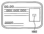
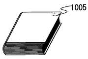
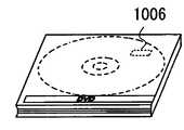
지폐 및 동전은 시장에서 유통되는 화폐이며, 특정한 지역에서 화폐와 같이 통용하는 것(금권), 기념 코인 등을 포함한다. 유가 증권류는 수표, 증권, 약속 어음 등을 포함하고, 프로세서 회로를 갖는 칩(1001)을 설치할 수 있다(도 8a 참조). 증서류는 운전면허증, 주민등록증 등을 가리키고, 프로세서 회로를 갖는 칩(1002)을 설치할 수 있다(도 8b 참조). 신변품은 가방, 안경 등을 포함하고, 프로세서 회로를 갖는 칩(1003)을 설치할 수 있다(도 8c 참조). 무기명 채권류는 우표, 라이스 쿠폰, 각종 상품권 등을 가리킨다. 포장용 용기류는 도시락 등의 포장지, 플라스틱 병 등을 가리키고, 프로세서 회로를 갖는 칩(1004)을 설치할 수 있다(도 8d 참조). 서적류는 서적, 책 등을 가리키고, 프로세서 회로를 갖는 칩(1005)을 설치할 수 있다(도 8e 참조). 기록 매체는 DVD 소프트웨어, 비디오 테이프 등을 가리키고, 프로세서 회로를 갖는 칩(1006)을 설치할 수 있다(도 8f 참조). 차량류는 자전거 등의 차량, 선박 등을 가리키고, 프로세서 회로를 갖는 칩(1007)을 설치할 수 있다(도 8g 참조). 식품류는 식료품, 음료 등을 가리킨다. 의류는 의복, 신발 등을 가리킨다. 보건 용품류는 의료 기구, 건강 기구 등을 가리킨다. 생활 용품류는 가구, 조명 기구 등을 가리킨다. 약품류는 의약품, 농약 등을 가리킨다. 전자 기기는 액정 표시 장치, EL 표시 장치, 텔레비전 세트(텔레비전 수상기, 박형 텔레비전 수상기), 휴대 전화 등을 가리킨다.Banknotes and coins are money that is circulated in the market, including money (pennies) and commemorative coins in certain areas. The securities include securities, promissory notes and the like, and a
이러한 반도체 장치는 물품의 표면에 부착하거나 물품에 매립해서 설치할 수 있다. 예를 들어, 책의 경우에는 반도체 장치를 책에 매립하면 좋고, 유기 수지로 이루어지는 패키지의 경우에는 반도체 장치를 유기 수지에 매립하면 좋다.Such a semiconductor device can be attached to the surface of the article or embedded in the article. For example, in the case of a book, a semiconductor device may be embedded in a book, and in the case of a package made of an organic resin, a semiconductor device may be embedded in an organic resin.
상술한 바와 같이, 포장용 용기류, 기록 매체, 신변품, 식품류, 의류, 생활 용품류, 전자 기기 등에 반도체 장치를 설치함으로써, 검사 시스템이나 렌탈점의 시스템 등의 효율화를 향상시킬 수 있다. 또한, 차량류에 반도체 장치를 설치함으로써, 위조나 도난을 방지할 수 있다. 또한, 동물 등의 생물에게 반도체 장치를 매립함으로써, 개개의 생물을 용이하게 식별할 수 있다. 예를 들어, 가축 등의 생물에게 센서를 구비한 반도체 장치를 이식/부착함으로써, 출생년이나 성별 또는 종류 등은 물론 현재 체온 등의 건강 상태를 용이하게 관리하는 것이 가능하게 된다.As described above, the efficiency of the inspection system, the rental point system, and the like can be improved by installing the semiconductor device in packaging containers, recording media, personal effects, foods, clothes, household goods, In addition, by installing a semiconductor device in a vehicle, it is possible to prevent forgery or theft. Further, by embedding a semiconductor device in an organism such as an animal, individual organisms can be easily identified. For example, by implanting / attaching a semiconductor device provided with a sensor to a creature such as a livestock, it becomes possible to easily manage a health state such as a current body temperature as well as a birth year, a sex, or a kind.
또한, 본 실시 형태는 실시 형태 1 내지 실시 형태 7 및 실시예1 중 어느 것과 적절히 조합하여 실시하는 것이 가능하다.The present embodiment can be implemented in any combination of any of
[실시예1][Example 1]
실시예1에서는 실시 형태 3에서 설명한, 도전성 차폐체를 IC 칩의 상하 양면에 설치하는 구조를 갖는 무선 칩과, 도전성 차폐체를 설치하지 않은 무선 칩을 형성하고, IC 칩의 공진 용량을 측정하여 비교한 결과에 대해서 설명한다.
도 9는 본 발명의 실시 형태에 따른 도전성 차폐체를 구비한 무선 칩과, 도전성 차폐체를 갖지 않은 종래의 무선 칩의 IC 칩 내의 공진 용량에 대한 공진 주파수의 측정 결과를 나타내고 있다. 각각의 무선 칩은 6mm의 크기(안테나의 최외주의 일단부로부터 타단부까지의 길이)를 갖는 안테나를 구비한다. 종축에 공진 주파수(MHz)를, 횡축에 칩 내의 공진 용량(pF)을 도시한다.Fig. 9 shows the results of measurement of the resonance frequency with respect to the resonance capacities in the IC chip of the conventional radio chip having no conductive shield and the radio chip having the conductive shield according to the embodiment of the present invention. Each of the wireless chips has an antenna having a size of 6 mm (the length from the one end to the other end of the outermost periphery of the antenna). The resonance frequency (MHz) on the ordinate, and the resonance capacitance (pF) in the chip on the abscissa.
또한, 이 경우에 측정에 사용되는 안테나는 선 폭이 135μm, 선간 거리가 5μm, 코일수가 15이다. 또한, 이 경우에 측정에 사용한 안테나는 Al을 사용하여, 5μm의 두께로 형성된다. IC 칩의 칩 내의 공진 용량의 조건을 24, 32 및 42pF로 하여, 본 발명의 실시 형태에 따른 도전성 차폐체를 갖는 무선 칩과, 도전성 차폐체를 갖고 있지 않은 종래의 무선 칩에 대해서 측정을 행했다.In this case, the antenna used for the measurement has a line width of 135 mu m, a line-to-line distance of 5 mu m, and a coil number of 15. In this case, the antenna used for the measurement is formed to a thickness of 5 mu m using Al. Measurements were conducted on a wireless chip having a conductive shield according to an embodiment of the present invention and a conventional wireless chip having no conductive shield, with the resonance capacitance conditions of the IC chip being 24, 32, and 42 pF.
예를 들어 원하는 공진 주파수가 13.5MHz인 경우, 본 발명의 실시 형태에 따른 도전성 차폐체를 갖는 무선 칩에 필요한 칩 내의 공진 용량은 약 29pF이다. 한편, 도전성 차폐체를 갖지 않는 무선 칩에 필요한 칩 내의 공진 용량은 약 35pF이다.For example, when the desired resonance frequency is 13.5 MHz, the resonance capacitance in a chip required for a wireless chip having a conductive shield according to the embodiment of the present invention is about 29 pF. On the other hand, the resonance capacity in a chip required for a wireless chip without a conductive shield is about 35 pF.
즉, 도전성 차폐체를 설치함으로써, 칩 내의 공진 용량을 약 6pF 저감할 수 있다.That is, by providing the conductive shield, the resonance capacity in the chip can be reduced by about 6 pF.
이어서, 안테나 크기가 8mm(안테나의 최외주의 일단부로부터 타단부까지의 길이)인 무선 칩의 IC 칩 내의 공진 용량에 대한 공진 주파수의 측정 결과를 도 10에 나타낸다. 또한, 종축에 공진 주파수를, 횡축에 칩 내의 공진 용량을 도시한다.10 shows the result of measurement of the resonance frequency with respect to the resonance capacity of the IC chip of the radio chip whose antenna size is 8 mm (the length from one end to the other end of the outermost periphery of the antenna). The ordinate indicates the resonance frequency, and the abscissa indicates the resonance capacitance in the chip.
또한, 이 경우 측정에 사용한 안테나는 선 폭이 105μm, 선간 거리가 5μm, 코일수가 17이다. 안테나는 Al을 사용하여, 5μm의 두께로 형성된다. IC 칩의 칩 내의 공진 용량의 조건을 20, 28 및 38pF로 하여, 본 발명의 실시 형태에 따른 도전성 차폐체를 갖는 무선 칩과, 도전성 차폐체를 갖고 있지 않은 종래의 무선 칩에 대해서 측정을 행했다.In this case, the antenna used for measurement has a line width of 105 mu m, a line-to-line distance of 5 mu m, and a number of coils of 17. The antenna is formed to a thickness of 5 mu m using Al. Measurement was performed on a wireless chip having a conductive shield according to the embodiment of the present invention and a conventional wireless chip having no conductive shield, with the conditions of the resonance capacities in the chip of the IC chip being 20, 28 and 38 pF.
예를 들어 원하는 공진 주파수가 13.5MHz인 경우, 본 발명의 실시 형태에 따른 도전성 차폐체를 갖는 무선 칩에 필요한 칩 내의 공진 용량은 약 24pF이다. 한편, 도전성 차폐체를 갖지 않는 무선 칩에 필요한 칩 내의 공진 용량은 약 35pF이다.For example, when the desired resonance frequency is 13.5 MHz, the resonance capacity in a chip required for a wireless chip having a conductive shield according to the embodiment of the present invention is about 24 pF. On the other hand, the resonance capacity in a chip required for a wireless chip without a conductive shield is about 35 pF.
즉, 도전성 차폐체를 설치함으로써, 칩 내의 공진 용량을 약 11pF 저감할 수 있다.That is, by providing the conductive shield, the resonance capacity in the chip can be reduced by about 11 pF.
상기 도 9 및 도 10에 도시한 측정 결과에 따르면, 도전성 차폐체를 설치함으로써, IC 칩 내의 공진 용량을 저감할 수 있고, 이는 IC 칩의 소형화를 유도한다는 것을 알았다.According to the measurement results shown in Figs. 9 and 10, it was found that the resonance capacity in the IC chip can be reduced by providing the conductive shield, which leads to miniaturization of the IC chip.
200: 무선 칩
201: 안테나
202: IC 칩
203: 기판
204: 공진 용량 소자부
205: 로직부
206a: 도전성 차폐체
206b: 도전성 차폐체
206c: 도전성 차폐체
207: 집적 회로
208: 결정성 반도체막
208a: 반도체막
208b: 반도체막
209: 게이트 절연막
210: 게이트 전극
211: 층간 절연막
212: 소스 또는 드레인 전극
213: 보호막
214a: 충격 확산층
214b: 충격 확산층
215a: 용량 소자
215b: 용량 소자
215c: 용량 소자
215d: 용량 소자
215e: 용량 소자
216: 층간 절연막
217: 배선
900: 기판
901: 박리층
902: 트랜지스터
903: 트랜지스터
904: 용량 소자
905: 절연층
910: 반도체 집적 회로
911: 안테나
912: 보호막
920: 충격 확산층
930: 충격 확산층
921: 섬유체
931: 섬유체
922: 유기 수지
932: 유기 수지
941: 분단면
1001-1007: 칩
1101-1103: 도전성 차폐체200: Wireless chip
201: antenna
202: IC chip
203: substrate
204: resonance capacitor element section
205:
206a: Conductive shield
206b: conductive shield
206c: conductive shield
207: Integrated Circuit
208: crystalline semiconductor film
208a: semiconductor film
208b: semiconductor film
209: Gate insulating film
210: gate electrode
211: interlayer insulating film
212: source or drain electrode
213: Shield
214a: Impact diffusion layer
214b: Impact diffusion layer
215a: Capacitive element
215b: Capacitive element
215c: Capacitive element
215d: Capacitive element
215e: Capacitive element
216: interlayer insulating film
217: Wiring
900: substrate
901: peeling layer
902: transistor
903: Transistor
904: Capacitive element
905: insulating layer
910: Semiconductor integrated circuit
911: Antenna
912: Shield
920: Impact diffusion layer
930: Impact diffusion layer
921: Fibers
931: Fibers
922: Organic resin
932: organic resin
941:
1001-1007: Chip
1101-1103: Conductive shield
Claims (25)
Translated fromKorean도전성 차폐체;
상기 도전성 차폐체 위에 구비된 제1 절연막;
배선을 포함하는 공진 용량 소자부와 집적 회로를 구비하고, 상기 제1 절연막 위에 구비된 IC 칩;
상기 IC 칩 위에 구비된 안테나; 및
상기 안테나 위에 구비된 제2 절연막;
을 포함하고,
상기 도전성 차폐체와 상기 안테나는 상기 제1 절연막을 개재하여 서로 적어도 일부가 겹치도록 구비되고,
상기 도전성 차폐체와 상기 안테나는 상기 제2 절연막을 개재하여 서로 적어도 일부가 겹치도록 구비되고,
상기 배선, 상기 제2 절연막 및 상기 도전성 차폐체는 용량 소자를 구성하고,
상기 도전성 차폐체는 상기 IC 칩을 둘러싸도록 구비되는, 반도체 장치.A semiconductor device comprising:
Conductive shield;
A first insulating layer provided on the conductive shield;
An IC chip provided on the first insulating film, the IC chip having a resonance capacitor element portion including wiring and an integrated circuit;
An antenna provided on the IC chip; And
A second insulating layer provided on the antenna;
/ RTI >
Wherein the conductive shield and the antenna are provided so that at least a part thereof overlaps each other via the first insulating film,
Wherein the conductive shield and the antenna are provided so that at least a part thereof overlaps each other via the second insulating film,
The wiring, the second insulating film, and the conductive shield constitute a capacitive element,
And the conductive shield member is provided so as to surround the IC chip.
도전성 차폐체;
상기 도전성 차폐체 위에 구비된 제1 절연막;
집적 회로를 구비하고, 상기 제1 절연막 위에 구비된 IC 칩;
상기 IC 칩 위에 구비된 안테나; 및
상기 안테나 위에 구비된 제2 절연막
을 포함하고,
상기 도전성 차폐체와 상기 안테나는 상기 제1 절연막을 개재하여 서로 적어도 일부가 겹치도록 구비되고,
상기 도전성 차폐체와 상기 안테나는 상기 제2 절연막을 개재하여 서로 적어도 일부가 겹치도록 구비되고,
상기 도전성 차폐체, 상기 제1 절연막 및 상기 안테나는 제1 용량 소자를 구성하고,
상기 도전성 차폐체, 상기 제2 절연막 및 상기 안테나는 제2 용량 소자를 구성하고,
상기 도전성 차폐체는 상기 IC 칩을 둘러싸도록 구비되는, 반도체 장치.A semiconductor device comprising:
Conductive shield;
A first insulating layer provided on the conductive shield;
An IC chip provided on the first insulating film and having an integrated circuit;
An antenna provided on the IC chip; And
The second insulating film
/ RTI >
Wherein the conductive shield and the antenna are provided so that at least a part thereof overlaps each other via the first insulating film,
Wherein the conductive shield and the antenna are provided so that at least a part thereof overlaps each other via the second insulating film,
The conductive shield, the first insulating film, and the antenna constitute a first capacitor,
The conductive shield, the second insulating film, and the antenna constitute a second capacitor,
And the conductive shield member is provided so as to surround the IC chip.
상기 제1 절연막과 상기 제2 절연막은 각각 충격 확산층을 포함하는, 반도체 장치.The method according to claim 1 or 4,
Wherein the first insulating film and the second insulating film each include an impurity diffusion layer.
상기 충격 확산층은, 섬유체에 유기 수지가 함침된(impregnated) 구조체인, 반도체 장치.6. The method of claim 5,
Wherein the impact diffusion layer is a structure in which a fibrous body is impregnated with an organic resin.
집적 회로를 구비한 IC 칩;
상기 IC 칩 위에 구비된 안테나; 및
절연막을 개재하여 상기 안테나와 적어도 일부 겹치도록 구비된 도전성 차폐체
를 포함하고,
상기 안테나, 상기 안테나 위의 상기 절연막, 및 상기 절연막 위의 상기 도전성 차폐체는 제1 용량 소자를 구성하고,
상기 도전성 차폐체는 상기 IC 칩을 둘러싸도록 구비되는, 반도체 장치.A semiconductor device comprising:
An IC chip having an integrated circuit;
An antenna provided on the IC chip; And
And a conductive shielding member provided so as to overlap at least a part of the antenna with an insulating film interposed therebetween.
Lt; / RTI >
Wherein the antenna, the insulating film on the antenna, and the conductive shield on the insulating film constitute a first capacitor,
And the conductive shield member is provided so as to surround the IC chip.
도전성 차폐체;
상기 도전성 차폐체 위에 구비된 절연막;
집적 회로를 구비하고, 상기 절연막 위에 구비된 IC 칩; 및
상기 IC 칩 위에 구비된 안테나
를 포함하고,
상기 도전성 차폐체와 상기 안테나는 상기 절연막을 개재하여 서로 적어도 일부가 겹치도록 구비되고,
상기 도전성 차폐체, 상기 절연막 및 상기 안테나는 제1 용량 소자를 구성하고,
상기 도전성 차폐체는 상기 IC 칩을 둘러싸도록 구비되는, 반도체 장치.A semiconductor device comprising:
Conductive shield;
An insulating film provided on the conductive shield;
An IC chip provided on the insulating film and having an integrated circuit; And
The antenna provided on the IC chip
Lt; / RTI >
Wherein the conductive shield member and the antenna are provided so that at least a part thereof overlaps each other via the insulating film,
The conductive shield, the insulating film, and the antenna constitute a first capacitor,
And the conductive shield member is provided so as to surround the IC chip.
집적 회로를 구비한 IC 칩;
상기 IC 칩 위에 구비된 안테나;
상기 안테나 위에 구비된 절연막; 및
상기 IC 칩을 둘러싸도록 구비된 도전성 차폐체
를 포함하고,
상기 안테나, 상기 절연막 및 상기 도전성 차폐체는 제1 용량 소자를 구성하는, 반도체 장치.A semiconductor device comprising:
An IC chip having an integrated circuit;
An antenna provided on the IC chip;
An insulating film provided on the antenna; And
And a conductive shielding member
Lt; / RTI >
Wherein the antenna, the insulating film, and the conductive shield constitute a first capacitor.
상기 IC 칩은 공진 용량 소자부를 더 구비하는, 반도체 장치.The method according to any one of claims 7, 11 and 15,
Wherein the IC chip further comprises a resonance capacitor element part.
상기 공진 용량 소자부는 배선을 포함하고,
상기 공진 용량 소자부, 상기 절연막 및 상기 도전성 차폐체는 제2 용량 소자를 구성하는, 반도체 장치.17. The method of claim 16,
Wherein the resonance capacitor element portion includes a wiring,
Wherein the resonance capacitor element portion, the insulating film, and the conductive shield member constitute a second capacitor element.
상기 절연막은 충격 확산층을 포함하는, 반도체 장치.The method according to any one of claims 7, 11 and 15,
Wherein the insulating film includes an impurity diffusion layer.
제1 절연막;
집적 회로를 구비하고, 상기 제1 절연막 위에 구비된 IC 칩;
상기 IC 칩 위에 구비된 층간 절연막;
상기 층간 절연막 위에 구비된, 코일 형상을 갖는 안테나;
상기 안테나 위에 구비된 제2 절연막; 및
상기 제2 절연막 위에 있는 제1 부분, 및 상기 제1 절연막 아래에 있는 제2 부분을 포함하는 도전성 차폐체
를 포함하고,
상기 도전성 차폐체의 상기 제2 부분과 상기 안테나는, 상기 제1 절연막을 개재하여 서로 적어도 일부가 겹치도록 구비되고,
상기 도전성 차폐체의 상기 제1 부분과 상기 안테나는, 상기 제2 절연막을 개재하여 서로 적어도 일부가 겹치도록 구비되고,
상기 도전성 차폐체의 상기 제2 부분, 상기 제1 절연막 및 상기 안테나는 제1 용량 소자를 구성하고,
상기 도전성 차폐체의 상기 제1 부분, 상기 제2 절연막 및 상기 안테나는 제2 용량 소자를 구성하고,
상기 도전성 차폐체는 상기 IC 칩을 둘러싸도록 구비되는, 반도체 장치.A semiconductor device comprising:
A first insulating film;
An IC chip provided on the first insulating film and having an integrated circuit;
An interlayer insulating film provided on the IC chip;
An antenna having a coil shape provided on the interlayer insulating film;
A second insulating layer provided on the antenna; And
A first portion on the second insulating film, and a second portion under the first insulating film,
Lt; / RTI >
The second portion of the conductive shield and the antenna are provided so that at least a part thereof overlaps each other via the first insulating film,
Wherein the first portion of the conductive shield and the antenna are provided so that at least a part thereof overlaps each other via the second insulating film,
The second portion of the conductive shield, the first insulating film, and the antenna constitute a first capacitor,
The first portion of the conductive shield, the second insulating film, and the antenna constitute a second capacitor,
And the conductive shield member is provided so as to surround the IC chip.
제1 절연막;
집적 회로를 구비하고, 상기 제1 절연막의 상면 위에 구비된 IC 칩;
상기 IC 칩 위에 구비된 층간 절연막;
상기 층간 절연막 위에 구비된, 코일 형상을 갖는 안테나;
상기 안테나 위에 구비된 제2 절연막; 및
상기 제2 절연막의 상면 위에 있는 제1 부분, 상기 제1 절연막의 하면 아래에 있는 제2 부분, 및 상기 제1 절연막의 측면 및 상기 제2 절연막의 측면과 접하는 제3 부분을 포함하는 도전성 차폐체
를 포함하고,
상기 안테나, 상기 제2 절연막, 및 상기 도전성 차폐체의 상기 제1 부분은 제1 용량 소자를 구성하고,
상기 도전성 차폐체는 상기 IC 칩을 둘러싸도록 구비되는, 반도체 장치.A semiconductor device comprising:
A first insulating film;
An IC chip provided on an upper surface of the first insulating film, the IC chip having an integrated circuit;
An interlayer insulating film provided on the IC chip;
An antenna having a coil shape provided on the interlayer insulating film;
A second insulating layer provided on the antenna; And
And a third portion that is in contact with a side surface of the first insulating film and a side surface of the second insulating film, and a second portion that is on the upper surface of the second insulating film, a second portion that is below the lower surface of the first insulating film,
Lt; / RTI >
Wherein the antenna, the second insulating film, and the first portion of the conductive shield constitute a first capacitor,
And the conductive shield member is provided so as to surround the IC chip.
상기 IC 칩은 트랜지스터를 포함하고,
상기 트랜지스터는 산화물 반도체층을 포함하는, 반도체 장치.21. The method according to claim 19 or 20,
Wherein the IC chip includes a transistor,
Wherein the transistor comprises an oxide semiconductor layer.
상기 제1 절연막과 상기 도전성 차폐체의 상기 제2 부분 사이의 제1 충격 확산층; 및
상기 제2 절연막과 상기 도전성 차폐체의 상기 제1 부분 사이의 제2 충격 확산층을 더 포함하는, 반도체 장치.21. The method according to claim 19 or 20,
A first shock-absorbing layer between the first insulating film and the second portion of the conductive shield; And
And a second impurity diffusion layer between the second insulating film and the first portion of the conductive shield.
상기 제1 충격 확산층과 상기 제2 충격 확산층 각각은, 섬유체에 유기 수지가 함침된 구조체인, 반도체 장치.23. The method of claim 22,
Wherein each of the first impact diffusion layer and the second impact diffusion layer is a structure in which a fibrous body is impregnated with an organic resin.
상기 IC 칩은 공진 용량 소자부를 더 구비하는, 반도체 장치.21. The method of claim 20,
Wherein the IC chip further comprises a resonance capacitor element part.
상기 공진 용량 소자부는 배선을 포함하고,
상기 공진 용량 소자부, 상기 제2 절연막, 및 상기 도전성 차폐체의 상기 제1 부분은 제2 용량 소자를 구성하는, 반도체 장치.25. The method of claim 24,
Wherein the resonance capacitor element portion includes a wiring,
Wherein the resonance capacitor element portion, the second insulating film, and the first portion of the conductive shield constitute a second capacitor element.
Applications Claiming Priority (2)
| Application Number | Priority Date | Filing Date | Title |
|---|---|---|---|
| JPJP-P-2008-256056 | 2008-10-01 | ||
| JP2008256056 | 2008-10-01 |
Publications (2)
| Publication Number | Publication Date |
|---|---|
| KR20110066956A KR20110066956A (en) | 2011-06-17 |
| KR101611643B1true KR101611643B1 (en) | 2016-04-11 |
Family
ID=42056503
Family Applications (1)
| Application Number | Title | Priority Date | Filing Date |
|---|---|---|---|
| KR1020117009849AExpired - Fee RelatedKR101611643B1 (en) | 2008-10-01 | 2009-09-07 | Semiconductor device |
Country Status (5)
| Country | Link |
|---|---|
| US (1) | US9196593B2 (en) |
| JP (1) | JP5637672B2 (en) |
| KR (1) | KR101611643B1 (en) |
| TW (1) | TWI478311B (en) |
| WO (1) | WO2010038599A1 (en) |
Families Citing this family (9)
| Publication number | Priority date | Publication date | Assignee | Title |
|---|---|---|---|---|
| PH12012500375A1 (en)* | 2009-08-26 | 2012-10-22 | Toppan Printing Co Ltd | Contactless communication medium |
| JP5501174B2 (en)* | 2009-09-17 | 2014-05-21 | 株式会社半導体エネルギー研究所 | Semiconductor device |
| JP6283558B2 (en) | 2014-04-22 | 2018-02-21 | 新光電気工業株式会社 | Passive element substrate |
| JP2015216072A (en) | 2014-05-13 | 2015-12-03 | 株式会社ジャパンディスプレイ | Organic EL device and manufacturing method thereof |
| JP6560610B2 (en)* | 2015-12-18 | 2019-08-14 | 株式会社ジャパンディスプレイ | Display device |
| US11073958B2 (en)* | 2016-01-29 | 2021-07-27 | Sharp Kabushiki Kaisha | Antenna device |
| JP6762004B2 (en)* | 2016-03-11 | 2020-09-30 | 国立大学法人九州工業大学 | Semiconductor integrated circuit equipment and its manufacturing method |
| JP7199174B2 (en)* | 2018-07-26 | 2023-01-05 | 東京エレクトロン株式会社 | Etching method |
| JP6546711B1 (en)* | 2019-04-10 | 2019-07-17 | 株式会社エスケーエレクトロニクス | Non-contact information carrier |
Citations (3)
| Publication number | Priority date | Publication date | Assignee | Title |
|---|---|---|---|---|
| JP2006108654A (en)* | 2004-09-09 | 2006-04-20 | Semiconductor Energy Lab Co Ltd | Radio chip |
| JP2007005778A (en)* | 2005-05-27 | 2007-01-11 | Semiconductor Energy Lab Co Ltd | Semiconductor device |
| JP2007241999A (en)* | 2006-02-08 | 2007-09-20 | Semiconductor Energy Lab Co Ltd | Semiconductor device |
Family Cites Families (179)
| Publication number | Priority date | Publication date | Assignee | Title |
|---|---|---|---|---|
| US4373163A (en)* | 1980-07-14 | 1983-02-08 | I.D. Engineering, Inc. | Loop antenna for security systems |
| JPS60198861A (en) | 1984-03-23 | 1985-10-08 | Fujitsu Ltd | Thin film transistor |
| JPH0244256B2 (en) | 1987-01-28 | 1990-10-03 | Kagaku Gijutsucho Mukizaishitsu Kenkyushocho | INGAZN2O5DESHIMESARERUROTSUHOSHOKEINOSOJOKOZOOJUSURUKAGOBUTSUOYOBISONOSEIZOHO |
| JPH0244258B2 (en) | 1987-02-24 | 1990-10-03 | Kagaku Gijutsucho Mukizaishitsu Kenkyushocho | INGAZN3O6DESHIMESARERUROTSUHOSHOKEINOSOJOKOZOOJUSURUKAGOBUTSUOYOBISONOSEIZOHO |
| JPH0244260B2 (en) | 1987-02-24 | 1990-10-03 | Kagaku Gijutsucho Mukizaishitsu Kenkyushocho | INGAZN5O8DESHIMESARERUROTSUHOSHOKEINOSOJOKOZOOJUSURUKAGOBUTSUOYOBISONOSEIZOHO |
| JPS63210023A (en) | 1987-02-24 | 1988-08-31 | Natl Inst For Res In Inorg Mater | Compound having a hexagonal layered structure represented by InGaZn↓4O↓7 and its manufacturing method |
| JPH0244262B2 (en) | 1987-02-27 | 1990-10-03 | Kagaku Gijutsucho Mukizaishitsu Kenkyushocho | INGAZN6O9DESHIMESARERUROTSUHOSHOKEINOSOJOKOZOOJUSURUKAGOBUTSUOYOBISONOSEIZOHO |
| JPH0244263B2 (en) | 1987-04-22 | 1990-10-03 | Kagaku Gijutsucho Mukizaishitsu Kenkyushocho | INGAZN7O10DESHIMESARERUROTSUHOSHOKEINOSOJOKOZOOJUSURUKAGOBUTSUOYOBISONOSEIZOHO |
| DE69032210D1 (en) | 1989-01-25 | 1998-05-07 | Asahi Chemical Ind | PRE-IMPREGNATED COMPOSITE MOLDS AND PRODUCTION OF A COMPOSITE MOLD |
| DE3907757A1 (en) | 1989-03-10 | 1990-09-13 | Mtu Muenchen Gmbh | PROTECTIVE FILM |
| JPH05190582A (en) | 1992-01-08 | 1993-07-30 | Oki Electric Ind Co Ltd | Resin sealed semiconductor device and manufacture thereof |
| JPH05251705A (en) | 1992-03-04 | 1993-09-28 | Fuji Xerox Co Ltd | Thin-film transistor |
| US5677045A (en) | 1993-09-14 | 1997-10-14 | Hitachi, Ltd. | Laminate and multilayer printed circuit board |
| JP3364081B2 (en) | 1995-02-16 | 2003-01-08 | 株式会社半導体エネルギー研究所 | Method for manufacturing semiconductor device |
| US5757456A (en) | 1995-03-10 | 1998-05-26 | Semiconductor Energy Laboratory Co., Ltd. | Display device and method of fabricating involving peeling circuits from one substrate and mounting on other |
| JP3406727B2 (en) | 1995-03-10 | 2003-05-12 | 株式会社半導体エネルギー研究所 | Display device |
| JP3479375B2 (en) | 1995-03-27 | 2003-12-15 | 科学技術振興事業団 | Metal oxide semiconductor device in which a pn junction is formed with a thin film transistor made of a metal oxide semiconductor such as cuprous oxide, and methods for manufacturing the same |
| US6323550B1 (en) | 1995-06-06 | 2001-11-27 | Analog Devices, Inc. | Package for sealing an integrated circuit die |
| KR100394896B1 (en) | 1995-08-03 | 2003-11-28 | 코닌클리케 필립스 일렉트로닉스 엔.브이. | A semiconductor device including a transparent switching element |
| JP3468954B2 (en) | 1995-12-01 | 2003-11-25 | 日立化成工業株式会社 | IC card |
| US5679975A (en) | 1995-12-18 | 1997-10-21 | Integrated Device Technology, Inc. | Conductive encapsulating shield for an integrated circuit |
| JP3625598B2 (en) | 1995-12-30 | 2005-03-02 | 三星電子株式会社 | Manufacturing method of liquid crystal display device |
| JPH10129165A (en) | 1996-03-15 | 1998-05-19 | Hitachi Maxell Ltd | Information carrier and method of manufacturing the same |
| JP2809200B2 (en) | 1996-06-03 | 1998-10-08 | 日本電気株式会社 | Method for manufacturing semiconductor device |
| US6482495B1 (en) | 1996-09-04 | 2002-11-19 | Hitachi Maxwell, Ltd. | Information carrier and process for production thereof |
| JPH1092980A (en) | 1996-09-13 | 1998-04-10 | Toshiba Corp | Wireless card and method of manufacturing the same |
| FR2755303A1 (en)* | 1996-10-25 | 1998-04-30 | Gemplus Sca | SHIELDED MAGNETIC FIELD ANTENNA IN A PRINTED CIRCUIT |
| JPH10181261A (en) | 1996-12-20 | 1998-07-07 | Dainippon Printing Co Ltd | Non-contact IC card |
| JPH10198778A (en) | 1997-01-14 | 1998-07-31 | Rohm Co Ltd | Ic card |
| JPH10211784A (en) | 1997-01-31 | 1998-08-11 | Denso Corp | Ic card and its manufacture |
| JP3500908B2 (en) | 1997-04-28 | 2004-02-23 | 松下電器産業株式会社 | Card reader |
| JPH11317475A (en) | 1998-02-27 | 1999-11-16 | Canon Inc | Semiconductor encapsulant resin and semiconductor element |
| JPH11353440A (en) | 1998-06-09 | 1999-12-24 | Kyodo Printing Co Ltd | Capacitors and contactless IC cards |
| JP4170454B2 (en) | 1998-07-24 | 2008-10-22 | Hoya株式会社 | Article having transparent conductive oxide thin film and method for producing the same |
| JP2000150861A (en) | 1998-11-16 | 2000-05-30 | Tdk Corp | Oxide thin film |
| JP3276930B2 (en) | 1998-11-17 | 2002-04-22 | 科学技術振興事業団 | Transistor and semiconductor device |
| TW484101B (en) | 1998-12-17 | 2002-04-21 | Hitachi Ltd | Semiconductor device and its manufacturing method |
| JP2000231619A (en) | 1999-02-10 | 2000-08-22 | Nippon Telegr & Teleph Corp <Ntt> | Contact type IC card |
| US6224965B1 (en) | 1999-06-25 | 2001-05-01 | Honeywell International Inc. | Microfiber dielectrics which facilitate laser via drilling |
| TW460731B (en) | 1999-09-03 | 2001-10-21 | Ind Tech Res Inst | Electrode structure and production method of wide viewing angle LCD |
| JP4423779B2 (en) | 1999-10-13 | 2010-03-03 | 味の素株式会社 | Epoxy resin composition, adhesive film and prepreg using the composition, multilayer printed wiring board using the same, and method for producing the same |
| JP4495295B2 (en) | 2000-03-15 | 2010-06-30 | 株式会社日立製作所 | Method for preventing unauthorized use of securities and system for preventing unauthorized use of securities |
| JP4347496B2 (en) | 2000-03-31 | 2009-10-21 | 共同印刷株式会社 | Method for producing reversible thermosensitive recording medium |
| JP2002043516A (en) | 2000-07-19 | 2002-02-08 | Toshiba Microelectronics Corp | Semiconductor device and memory device |
| JP4302859B2 (en) | 2000-08-04 | 2009-07-29 | 日立化成工業株式会社 | Non-contact IC tag |
| JP4089858B2 (en) | 2000-09-01 | 2008-05-28 | 国立大学法人東北大学 | Semiconductor device |
| KR20020038482A (en) | 2000-11-15 | 2002-05-23 | 모리시타 요이찌 | Thin film transistor array, method for producing the same, and display panel using the same |
| JP4565595B2 (en) | 2001-02-16 | 2010-10-20 | トッパン・フォームズ株式会社 | Non-contact type antenna for data transceiver and its capacitance adjustment method |
| JP3997731B2 (en) | 2001-03-19 | 2007-10-24 | 富士ゼロックス株式会社 | Method for forming a crystalline semiconductor thin film on a substrate |
| JP2002289859A (en) | 2001-03-23 | 2002-10-04 | Minolta Co Ltd | Thin film transistor |
| JP3939504B2 (en)* | 2001-04-17 | 2007-07-04 | カシオ計算機株式会社 | Semiconductor device, method for manufacturing the same, and mounting structure |
| TW564471B (en) | 2001-07-16 | 2003-12-01 | Semiconductor Energy Lab | Semiconductor device and peeling off method and method of manufacturing semiconductor device |
| JP4027740B2 (en) | 2001-07-16 | 2007-12-26 | 株式会社半導体エネルギー研究所 | Method for manufacturing semiconductor device |
| JP4090716B2 (en) | 2001-09-10 | 2008-05-28 | 雅司 川崎 | Thin film transistor and matrix display device |
| JP3925839B2 (en) | 2001-09-10 | 2007-06-06 | シャープ株式会社 | Semiconductor memory device and test method thereof |
| JP4164562B2 (en) | 2002-09-11 | 2008-10-15 | 独立行政法人科学技術振興機構 | Transparent thin film field effect transistor using homologous thin film as active layer |
| WO2003040441A1 (en) | 2001-11-05 | 2003-05-15 | Japan Science And Technology Agency | Natural superlattice homologous single crystal thin film, method for preparation thereof, and device using said single crystal thin film |
| JP2003141486A (en) | 2001-11-08 | 2003-05-16 | Oji Paper Co Ltd | Non-contact IC card and method of manufacturing the same |
| KR100430001B1 (en) | 2001-12-18 | 2004-05-03 | 엘지전자 주식회사 | Manufacturing method of multi-layer pcb, pad fabricating method of multi-layer pcb, semiconductor pkg manufacturing method using multi-layer pcb |
| JP4083486B2 (en) | 2002-02-21 | 2008-04-30 | 独立行政法人科学技術振興機構 | Method for producing LnCuO (S, Se, Te) single crystal thin film |
| CN1445821A (en) | 2002-03-15 | 2003-10-01 | 三洋电机株式会社 | Forming method of ZnO film and ZnO semiconductor layer, semiconductor element and manufacturing method thereof |
| JP3933591B2 (en) | 2002-03-26 | 2007-06-20 | 淳二 城戸 | Organic electroluminescent device |
| US7339187B2 (en) | 2002-05-21 | 2008-03-04 | State Of Oregon Acting By And Through The Oregon State Board Of Higher Education On Behalf Of Oregon State University | Transistor structures |
| JP2004022625A (en) | 2002-06-13 | 2004-01-22 | Murata Mfg Co Ltd | Semiconductor device and method of manufacturing the semiconductor device |
| US7485489B2 (en) | 2002-06-19 | 2009-02-03 | Bjoersell Sten | Electronics circuit manufacture |
| EP1514307A1 (en) | 2002-06-19 | 2005-03-16 | Sten Bjorsell | Electronics circuit manufacture |
| US7105868B2 (en) | 2002-06-24 | 2006-09-12 | Cermet, Inc. | High-electron mobility transistor with zinc oxide |
| US7132311B2 (en) | 2002-07-26 | 2006-11-07 | Intel Corporation | Encapsulation of a stack of semiconductor dice |
| JP2004094492A (en) | 2002-08-30 | 2004-03-25 | Konica Minolta Holdings Inc | Ic card |
| JP4012025B2 (en) | 2002-09-24 | 2007-11-21 | 大日本印刷株式会社 | Manufacturing method of film with microstructure and film with microstructure |
| US7067843B2 (en) | 2002-10-11 | 2006-06-27 | E. I. Du Pont De Nemours And Company | Transparent oxide semiconductor thin film transistors |
| JP4004929B2 (en)* | 2002-10-31 | 2007-11-07 | トッパン・フォームズ株式会社 | Non-contact type data receiving / transmitting body and capacitance adjusting method thereof |
| JP4166105B2 (en) | 2003-03-06 | 2008-10-15 | シャープ株式会社 | Semiconductor device and manufacturing method thereof |
| JP2004273732A (en) | 2003-03-07 | 2004-09-30 | Sharp Corp | Active matrix substrate and manufacturing method thereof |
| JP4828088B2 (en) | 2003-06-05 | 2011-11-30 | 凸版印刷株式会社 | IC tag |
| JP2004364199A (en)* | 2003-06-06 | 2004-12-24 | Sony Corp | Antenna module and portable communication terminal equipped therewith |
| JP4108633B2 (en) | 2003-06-20 | 2008-06-25 | シャープ株式会社 | THIN FILM TRANSISTOR, MANUFACTURING METHOD THEREOF, AND ELECTRONIC DEVICE |
| US7262463B2 (en) | 2003-07-25 | 2007-08-28 | Hewlett-Packard Development Company, L.P. | Transistor including a deposited channel region having a doped portion |
| US7566010B2 (en)* | 2003-12-26 | 2009-07-28 | Semiconductor Energy Laboratory Co., Ltd. | Securities, chip mounting product, and manufacturing method thereof |
| WO2005074030A1 (en) | 2004-01-30 | 2005-08-11 | Semiconductor Energy Laboratory Co., Ltd. | Semiconductor device |
| US7282782B2 (en) | 2004-03-12 | 2007-10-16 | Hewlett-Packard Development Company, L.P. | Combined binary oxide semiconductor device |
| US7297977B2 (en) | 2004-03-12 | 2007-11-20 | Hewlett-Packard Development Company, L.P. | Semiconductor device |
| US7145174B2 (en) | 2004-03-12 | 2006-12-05 | Hewlett-Packard Development Company, Lp. | Semiconductor device |
| CN1998087B (en) | 2004-03-12 | 2014-12-31 | 独立行政法人科学技术振兴机构 | Amorphous oxide and thin film transistor |
| EP1589797A3 (en) | 2004-04-19 | 2008-07-30 | Matsushita Electric Industrial Co., Ltd. | Manufacturing method of laminated substrate, and manufacturing apparatus of semiconductor device for module and laminated substrate for use therein |
| WO2005119781A1 (en) | 2004-06-02 | 2005-12-15 | Semiconductor Energy Laboratory Co., Ltd. | Laminating system |
| US7211825B2 (en) | 2004-06-14 | 2007-05-01 | Yi-Chi Shih | Indium oxide-based thin film transistors and circuits |
| US7534702B2 (en) | 2004-06-29 | 2009-05-19 | Semiconductor Energy Laboratory Co., Ltd. | Method for manufacturing a semiconductor device |
| US7591863B2 (en) | 2004-07-16 | 2009-09-22 | Semiconductor Energy Laboratory Co., Ltd. | Laminating system, IC sheet, roll of IC sheet, and method for manufacturing IC chip |
| WO2006022169A1 (en) | 2004-08-23 | 2006-03-02 | Semiconductor Energy Laboratory Co., Ltd. | Wireless chip and manufacturing method thereof |
| JP2006100760A (en) | 2004-09-02 | 2006-04-13 | Casio Comput Co Ltd | Thin film transistor and manufacturing method thereof |
| WO2006028195A1 (en)* | 2004-09-09 | 2006-03-16 | Semiconductor Energy Laboratory Co., Ltd. | Wireless chip |
| WO2006038438A2 (en) | 2004-09-14 | 2006-04-13 | Oji Paper Co | Reversible thermal recording material, and communication medium having display layer and recording material |
| US7285501B2 (en) | 2004-09-17 | 2007-10-23 | Hewlett-Packard Development Company, L.P. | Method of forming a solution processed device |
| US7298084B2 (en) | 2004-11-02 | 2007-11-20 | 3M Innovative Properties Company | Methods and displays utilizing integrated zinc oxide row and column drivers in conjunction with organic light emitting diodes |
| US7829444B2 (en) | 2004-11-10 | 2010-11-09 | Canon Kabushiki Kaisha | Field effect transistor manufacturing method |
| EP2453481B1 (en) | 2004-11-10 | 2017-01-11 | Canon Kabushiki Kaisha | Field effect transistor with amorphous oxide |
| US7791072B2 (en) | 2004-11-10 | 2010-09-07 | Canon Kabushiki Kaisha | Display |
| AU2005302964B2 (en) | 2004-11-10 | 2010-11-04 | Canon Kabushiki Kaisha | Field effect transistor employing an amorphous oxide |
| KR100953596B1 (en) | 2004-11-10 | 2010-04-21 | 캐논 가부시끼가이샤 | Light emitting device |
| US7863611B2 (en) | 2004-11-10 | 2011-01-04 | Canon Kabushiki Kaisha | Integrated circuits utilizing amorphous oxides |
| US7453065B2 (en) | 2004-11-10 | 2008-11-18 | Canon Kabushiki Kaisha | Sensor and image pickup device |
| CN101099165A (en)* | 2005-01-11 | 2008-01-02 | 富士通株式会社 | IC tag storing case |
| US7579224B2 (en) | 2005-01-21 | 2009-08-25 | Semiconductor Energy Laboratory Co., Ltd. | Method for manufacturing a thin film semiconductor device |
| TWI505473B (en) | 2005-01-28 | 2015-10-21 | Semiconductor Energy Lab | Semiconductor device, electronic device, and method of manufacturing semiconductor device |
| TWI445178B (en) | 2005-01-28 | 2014-07-11 | Semiconductor Energy Lab | Semiconductor device, electronic device, and method of manufacturing semiconductor device |
| US7858451B2 (en) | 2005-02-03 | 2010-12-28 | Semiconductor Energy Laboratory Co., Ltd. | Electronic device, semiconductor device and manufacturing method thereof |
| US7948171B2 (en) | 2005-02-18 | 2011-05-24 | Semiconductor Energy Laboratory Co., Ltd. | Light emitting device |
| US20060197092A1 (en) | 2005-03-03 | 2006-09-07 | Randy Hoffman | System and method for forming conductive material on a substrate |
| US8681077B2 (en) | 2005-03-18 | 2014-03-25 | Semiconductor Energy Laboratory Co., Ltd. | Semiconductor device, and display device, driving method and electronic apparatus thereof |
| US7544967B2 (en) | 2005-03-28 | 2009-06-09 | Massachusetts Institute Of Technology | Low voltage flexible organic/transparent transistor for selective gas sensing, photodetecting and CMOS device applications |
| US7645478B2 (en) | 2005-03-31 | 2010-01-12 | 3M Innovative Properties Company | Methods of making displays |
| US8300031B2 (en) | 2005-04-20 | 2012-10-30 | Semiconductor Energy Laboratory Co., Ltd. | Semiconductor device comprising transistor having gate and drain connected through a current-voltage conversion element |
| DE102005021825A1 (en) | 2005-05-11 | 2006-11-16 | Infineon Technologies Ag | Semiconductor memory device e.g. dynamic RAM, for writing/reading of information bits of charge storable/readable on trench condenser, has conductive shielding device formed between two parallely arranged bit lines and spaced from bit lines |
| US7923796B2 (en) | 2005-05-27 | 2011-04-12 | Semiconductor Energy Laboratory Co., Ltd. | Semiconductor device including resonance circuit |
| JP2007005782A (en) | 2005-05-27 | 2007-01-11 | Semiconductor Energy Lab Co Ltd | Semiconductor device and manufacturing method of semiconductor device |
| US7566971B2 (en) | 2005-05-27 | 2009-07-28 | Semiconductor Energy Laboratory Co., Ltd. | Semiconductor device and manufacturing method thereof |
| US7868320B2 (en)* | 2005-05-31 | 2011-01-11 | Semiconductor Energy Laboratory Co., Ltd. | Semiconductor device and manufacturing method thereof |
| JP2006344849A (en) | 2005-06-10 | 2006-12-21 | Casio Comput Co Ltd | Thin film transistor |
| US7402506B2 (en) | 2005-06-16 | 2008-07-22 | Eastman Kodak Company | Methods of making thin film transistors comprising zinc-oxide-based semiconductor materials and transistors made thereby |
| US7691666B2 (en) | 2005-06-16 | 2010-04-06 | Eastman Kodak Company | Methods of making thin film transistors comprising zinc-oxide-based semiconductor materials and transistors made thereby |
| US7507618B2 (en) | 2005-06-27 | 2009-03-24 | 3M Innovative Properties Company | Method for making electronic devices using metal oxide nanoparticles |
| US7727859B2 (en) | 2005-06-30 | 2010-06-01 | Semiconductor Energy Laboratory Co., Ltd | Semiconductor device and manufacturing method thereof |
| KR100711890B1 (en) | 2005-07-28 | 2007-04-25 | 삼성에스디아이 주식회사 | OLED display and manufacturing method thereof |
| JP2007059128A (en) | 2005-08-23 | 2007-03-08 | Canon Inc | Organic EL display device and manufacturing method thereof |
| JP2007059821A (en) | 2005-08-26 | 2007-03-08 | Shinko Electric Ind Co Ltd | Method for manufacturing wiring board |
| JP5116225B2 (en) | 2005-09-06 | 2013-01-09 | キヤノン株式会社 | Manufacturing method of oxide semiconductor device |
| JP4280736B2 (en) | 2005-09-06 | 2009-06-17 | キヤノン株式会社 | Semiconductor element |
| JP2007073705A (en) | 2005-09-06 | 2007-03-22 | Canon Inc | Oxide semiconductor channel thin film transistor and method for manufacturing the same |
| JP4850457B2 (en) | 2005-09-06 | 2012-01-11 | キヤノン株式会社 | Thin film transistor and thin film diode |
| EP1770788A3 (en) | 2005-09-29 | 2011-09-21 | Semiconductor Energy Laboratory Co., Ltd. | Semiconductor device having oxide semiconductor layer and manufacturing method thereof |
| CN101278398B (en) | 2005-09-30 | 2010-09-29 | 株式会社半导体能源研究所 | Method for manufacturing semiconductor device |
| WO2007043602A1 (en) | 2005-10-14 | 2007-04-19 | Semiconductor Energy Laboratory Co., Ltd. | Semiconductor device and communication system using the semiconductor device |
| JP4907292B2 (en) | 2005-10-14 | 2012-03-28 | 株式会社半導体エネルギー研究所 | Semiconductor device and communication system using the semiconductor device |
| JP5037808B2 (en) | 2005-10-20 | 2012-10-03 | キヤノン株式会社 | Field effect transistor using amorphous oxide, and display device using the transistor |
| CN101577231B (en) | 2005-11-15 | 2013-01-02 | 株式会社半导体能源研究所 | Semiconductor device and method of manufacturing the same |
| TWI292281B (en) | 2005-12-29 | 2008-01-01 | Ind Tech Res Inst | Pixel structure of active organic light emitting diode and method of fabricating the same |
| US7867636B2 (en) | 2006-01-11 | 2011-01-11 | Murata Manufacturing Co., Ltd. | Transparent conductive film and method for manufacturing the same |
| JP4977478B2 (en) | 2006-01-21 | 2012-07-18 | 三星電子株式会社 | ZnO film and method of manufacturing TFT using the same |
| JP4251185B2 (en) | 2006-01-23 | 2009-04-08 | ソニー株式会社 | Manufacturing method of semiconductor integrated circuit card |
| US7576394B2 (en) | 2006-02-02 | 2009-08-18 | Kochi Industrial Promotion Center | Thin film transistor including low resistance conductive thin films and manufacturing method thereof |
| DE602007013478D1 (en)* | 2006-02-08 | 2011-05-12 | Semiconductor Energy Lab | RFID device |
| US7977169B2 (en) | 2006-02-15 | 2011-07-12 | Kochi Industrial Promotion Center | Semiconductor device including active layer made of zinc oxide with controlled orientations and manufacturing method thereof |
| KR20070101595A (en) | 2006-04-11 | 2007-10-17 | 삼성전자주식회사 | ZnO TFT |
| US20070252928A1 (en) | 2006-04-28 | 2007-11-01 | Toppan Printing Co., Ltd. | Structure, transmission type liquid crystal display, reflection type display and manufacturing method thereof |
| JP2008040904A (en) | 2006-08-08 | 2008-02-21 | Hitachi Ltd | RFID tag and reading method thereof |
| TWI431726B (en) | 2006-06-01 | 2014-03-21 | Semiconductor Energy Lab | Non-volatile semiconductor memory device |
| JP5028033B2 (en) | 2006-06-13 | 2012-09-19 | キヤノン株式会社 | Oxide semiconductor film dry etching method |
| EP2038818B1 (en) | 2006-06-26 | 2014-10-15 | Semiconductor Energy Laboratory Co., Ltd. | Paper including semiconductor device and manufacturing method thereof |
| JP4609797B2 (en) | 2006-08-09 | 2011-01-12 | Nec液晶テクノロジー株式会社 | Thin film device and manufacturing method thereof |
| JP4999400B2 (en) | 2006-08-09 | 2012-08-15 | キヤノン株式会社 | Oxide semiconductor film dry etching method |
| KR101381359B1 (en) | 2006-08-31 | 2014-04-04 | 가부시키가이샤 한도오따이 에네루기 켄큐쇼 | Clock generation circuit and semiconductor device including the same |
| JP5063256B2 (en) | 2006-08-31 | 2012-10-31 | 株式会社半導体エネルギー研究所 | Clock generation circuit, counter circuit included in clock generation circuit, and semiconductor device |
| JP4332545B2 (en) | 2006-09-15 | 2009-09-16 | キヤノン株式会社 | Field effect transistor and manufacturing method thereof |
| JP5164357B2 (en) | 2006-09-27 | 2013-03-21 | キヤノン株式会社 | Semiconductor device and manufacturing method of semiconductor device |
| JP4274219B2 (en) | 2006-09-27 | 2009-06-03 | セイコーエプソン株式会社 | Electronic devices, organic electroluminescence devices, organic thin film semiconductor devices |
| US7622371B2 (en) | 2006-10-10 | 2009-11-24 | Hewlett-Packard Development Company, L.P. | Fused nanocrystal thin film semiconductor and method |
| US7772021B2 (en) | 2006-11-29 | 2010-08-10 | Samsung Electronics Co., Ltd. | Flat panel displays comprising a thin-film transistor having a semiconductive oxide in its channel and methods of fabricating the same for use in flat panel displays |
| JP2008140684A (en) | 2006-12-04 | 2008-06-19 | Toppan Printing Co Ltd | Color EL display and manufacturing method thereof |
| KR101303578B1 (en) | 2007-01-05 | 2013-09-09 | 삼성전자주식회사 | Etching method of thin film |
| US8207063B2 (en) | 2007-01-26 | 2012-06-26 | Eastman Kodak Company | Process for atomic layer deposition |
| US8009050B2 (en) | 2007-02-02 | 2011-08-30 | Semiconductor Energy Laboratory Co., Ltd. | Wireless system, semiconductor device, and communication device |
| EP1970951A3 (en) | 2007-03-13 | 2009-05-06 | Semiconductor Energy Laboratory Co., Ltd. | Semiconductor device and manufacturing method thereof |
| EP2372756A1 (en) | 2007-03-13 | 2011-10-05 | Semiconductor Energy Laboratory Co, Ltd. | Semiconductor device and manufacturing method thereof |
| KR100851215B1 (en) | 2007-03-14 | 2008-08-07 | 삼성에스디아이 주식회사 | Thin film transistor and organic light emitting display device using same |
| EP1976001A3 (en) | 2007-03-26 | 2012-08-22 | Semiconductor Energy Laboratory Co., Ltd. | Method for manufacturing semiconductor device |
| US7795613B2 (en) | 2007-04-17 | 2010-09-14 | Toppan Printing Co., Ltd. | Structure with transistor |
| KR101325053B1 (en) | 2007-04-18 | 2013-11-05 | 삼성디스플레이 주식회사 | Thin film transistor substrate and manufacturing method thereof |
| KR20080094300A (en) | 2007-04-19 | 2008-10-23 | 삼성전자주식회사 | Thin film transistors and methods of manufacturing the same and flat panel displays comprising thin film transistors |
| KR101334181B1 (en) | 2007-04-20 | 2013-11-28 | 삼성전자주식회사 | Thin Film Transistor having selectively crystallized channel layer and method of manufacturing the same |
| CN101663762B (en) | 2007-04-25 | 2011-09-21 | 佳能株式会社 | Oxynitride semiconductor |
| KR101345376B1 (en) | 2007-05-29 | 2013-12-24 | 삼성전자주식회사 | Fabrication method of ZnO family Thin film transistor |
| EP2001047A1 (en) | 2007-06-07 | 2008-12-10 | Semiconductor Energy Laboratory Co, Ltd. | Semiconductor device |
| EP2019425A1 (en) | 2007-07-27 | 2009-01-28 | Semiconductor Energy Laboratory Co., Ltd. | Semiconductor device and method for manufacturing the same |
| US8202365B2 (en) | 2007-12-17 | 2012-06-19 | Fujifilm Corporation | Process for producing oriented inorganic crystalline film, and semiconductor device using the oriented inorganic crystalline film |
| WO2009139282A1 (en) | 2008-05-12 | 2009-11-19 | Semiconductor Energy Laboratory Co., Ltd. | Semiconductor device and method for manufacturing semiconductor device |
| CN102037556B (en) | 2008-05-23 | 2016-02-10 | 株式会社半导体能源研究所 | Semiconductor device |
| JP4623179B2 (en) | 2008-09-18 | 2011-02-02 | ソニー株式会社 | Thin film transistor and manufacturing method thereof |
| JP5451280B2 (en) | 2008-10-09 | 2014-03-26 | キヤノン株式会社 | Wurtzite crystal growth substrate, manufacturing method thereof, and semiconductor device |
- 2009
- 2009-09-07KRKR1020117009849Apatent/KR101611643B1/ennot_activeExpired - Fee Related
- 2009-09-07WOPCT/JP2009/065970patent/WO2010038599A1/enactiveApplication Filing
- 2009-09-22TWTW098131934Apatent/TWI478311B/ennot_activeIP Right Cessation
- 2009-09-28USUS12/567,946patent/US9196593B2/ennot_activeExpired - Fee Related
- 2009-09-30JPJP2009226638Apatent/JP5637672B2/ennot_activeExpired - Fee Related
Patent Citations (3)
| Publication number | Priority date | Publication date | Assignee | Title |
|---|---|---|---|---|
| JP2006108654A (en)* | 2004-09-09 | 2006-04-20 | Semiconductor Energy Lab Co Ltd | Radio chip |
| JP2007005778A (en)* | 2005-05-27 | 2007-01-11 | Semiconductor Energy Lab Co Ltd | Semiconductor device |
| JP2007241999A (en)* | 2006-02-08 | 2007-09-20 | Semiconductor Energy Lab Co Ltd | Semiconductor device |
Also Published As
| Publication number | Publication date |
|---|---|
| TW201030930A (en) | 2010-08-16 |
| JP5637672B2 (en) | 2014-12-10 |
| US20100078787A1 (en) | 2010-04-01 |
| WO2010038599A1 (en) | 2010-04-08 |
| KR20110066956A (en) | 2011-06-17 |
| JP2010109351A (en) | 2010-05-13 |
| US9196593B2 (en) | 2015-11-24 |
| TWI478311B (en) | 2015-03-21 |
Similar Documents
| Publication | Publication Date | Title |
|---|---|---|
| KR101611643B1 (en) | Semiconductor device | |
| JP5460912B2 (en) | RFID tag | |
| TWI480806B (en) | Semiconductor device and wireless tag using the same | |
| US8698220B2 (en) | Semiconductor device having concentration difference of impurity element in semiconductor films | |
| JP5767690B2 (en) | Semiconductor device | |
| JP5937144B2 (en) | Bias circuit | |
| KR101628013B1 (en) | Semiconductor device and rfid tag using the semiconductor device | |
| WO2010035625A1 (en) | Semi conductor device | |
| US8540161B2 (en) | Semiconductor device and method for manufacturing the same |
Legal Events
| Date | Code | Title | Description |
|---|---|---|---|
| PA0105 | International application | St.27 status event code:A-0-1-A10-A15-nap-PA0105 | |
| E13-X000 | Pre-grant limitation requested | St.27 status event code:A-2-3-E10-E13-lim-X000 | |
| P11-X000 | Amendment of application requested | St.27 status event code:A-2-2-P10-P11-nap-X000 | |
| P13-X000 | Application amended | St.27 status event code:A-2-2-P10-P13-nap-X000 | |
| PG1501 | Laying open of application | St.27 status event code:A-1-1-Q10-Q12-nap-PG1501 | |
| P11-X000 | Amendment of application requested | St.27 status event code:A-2-2-P10-P11-nap-X000 | |
| P13-X000 | Application amended | St.27 status event code:A-2-2-P10-P13-nap-X000 | |
| PA0201 | Request for examination | St.27 status event code:A-1-2-D10-D11-exm-PA0201 | |
| D13-X000 | Search requested | St.27 status event code:A-1-2-D10-D13-srh-X000 | |
| D14-X000 | Search report completed | St.27 status event code:A-1-2-D10-D14-srh-X000 | |
| E902 | Notification of reason for refusal | ||
| PE0902 | Notice of grounds for rejection | St.27 status event code:A-1-2-D10-D21-exm-PE0902 | |
| P11-X000 | Amendment of application requested | St.27 status event code:A-2-2-P10-P11-nap-X000 | |
| P13-X000 | Application amended | St.27 status event code:A-2-2-P10-P13-nap-X000 | |
| E701 | Decision to grant or registration of patent right | ||
| PE0701 | Decision of registration | St.27 status event code:A-1-2-D10-D22-exm-PE0701 | |
| GRNT | Written decision to grant | ||
| PR0701 | Registration of establishment | St.27 status event code:A-2-4-F10-F11-exm-PR0701 | |
| PR1002 | Payment of registration fee | St.27 status event code:A-2-2-U10-U12-oth-PR1002 Fee payment year number:1 | |
| PG1601 | Publication of registration | St.27 status event code:A-4-4-Q10-Q13-nap-PG1601 | |
| PR1001 | Payment of annual fee | St.27 status event code:A-4-4-U10-U11-oth-PR1001 Fee payment year number:4 | |
| PC1903 | Unpaid annual fee | St.27 status event code:A-4-4-U10-U13-oth-PC1903 Not in force date:20200406 Payment event data comment text:Termination Category : DEFAULT_OF_REGISTRATION_FEE | |
| PC1903 | Unpaid annual fee | St.27 status event code:N-4-6-H10-H13-oth-PC1903 Ip right cessation event data comment text:Termination Category : DEFAULT_OF_REGISTRATION_FEE Not in force date:20200406 |