KR101610040B1 - Electroluminescent Display with Initial Nonuniformity Compensation - Google Patents
Electroluminescent Display with Initial Nonuniformity CompensationDownload PDFInfo
- Publication number
- KR101610040B1 KR101610040B1KR1020117008892AKR20117008892AKR101610040B1KR 101610040 B1KR101610040 B1KR 101610040B1KR 1020117008892 AKR1020117008892 AKR 1020117008892AKR 20117008892 AKR20117008892 AKR 20117008892AKR 101610040 B1KR101610040 B1KR 101610040B1
- Authority
- KR
- South Korea
- Prior art keywords
- transistor
- electrode
- lead
- subpixels
- voltage
- Prior art date
- Legal status (The legal status is an assumption and is not a legal conclusion. Google has not performed a legal analysis and makes no representation as to the accuracy of the status listed.)
- Active
Links
- 238000000034methodMethods0.000claimsabstractdescription41
- 238000012360testing methodMethods0.000claimsabstractdescription6
- 238000005259measurementMethods0.000claimsdescription32
- 239000011159matrix materialSubstances0.000claimsdescription12
- 229910021420polycrystalline siliconInorganic materials0.000claimsdescription4
- 229920005591polysiliconPolymers0.000claimsdescription4
- 230000008878couplingEffects0.000claimsdescription2
- 238000010168coupling processMethods0.000claimsdescription2
- 238000005859coupling reactionMethods0.000claimsdescription2
- YTAHJIFKAKIKAV-XNMGPUDCSA-N[(1R)-3-morpholin-4-yl-1-phenylpropyl] N-[(3S)-2-oxo-5-phenyl-1,3-dihydro-1,4-benzodiazepin-3-yl]carbamateChemical compoundO=C1[C@H](N=C(C2=C(N1)C=CC=C2)C1=CC=CC=C1)NC(O[C@H](CCN1CCOCC1)C1=CC=CC=C1)=OYTAHJIFKAKIKAV-XNMGPUDCSA-N0.000claims1
- 238000001914filtrationMethods0.000claims1
- 230000008569processEffects0.000description11
- 230000008901benefitEffects0.000description7
- 230000008859changeEffects0.000description7
- 238000010586diagramMethods0.000description7
- 238000006243chemical reactionMethods0.000description4
- 238000013459approachMethods0.000description3
- 238000012937correctionMethods0.000description3
- 230000006870functionEffects0.000description3
- 239000000758substrateSubstances0.000description3
- 239000010409thin filmSubstances0.000description3
- 230000000007visual effectEffects0.000description3
- 230000032683agingEffects0.000description2
- 229910021417amorphous siliconInorganic materials0.000description2
- 239000003990capacitorSubstances0.000description2
- 230000015556catabolic processEffects0.000description2
- 238000006731degradation reactionMethods0.000description2
- 230000000694effectsEffects0.000description2
- 238000005516engineering processMethods0.000description2
- 239000000463materialSubstances0.000description2
- 238000012545processingMethods0.000description2
- 240000000278Syzygium polyanthumSpecies0.000description1
- XLOMVQKBTHCTTD-UHFFFAOYSA-NZinc monoxideChemical compound[Zn]=OXLOMVQKBTHCTTD-UHFFFAOYSA-N0.000description1
- 230000003466anti-cipated effectEffects0.000description1
- 238000004422calculation algorithmMethods0.000description1
- 238000004364calculation methodMethods0.000description1
- 239000003086colorantSubstances0.000description1
- 230000001186cumulative effectEffects0.000description1
- 238000013479data entryMethods0.000description1
- 230000007547defectEffects0.000description1
- 230000008021depositionEffects0.000description1
- 230000002431foraging effectEffects0.000description1
- 230000001788irregularEffects0.000description1
- 230000007774longtermEffects0.000description1
- 238000004519manufacturing processMethods0.000description1
- 238000000691measurement methodMethods0.000description1
- 239000002096quantum dotSubstances0.000description1
- 238000004088simulationMethods0.000description1
- 239000007787solidSubstances0.000description1
- 235000013599spicesNutrition0.000description1
- 230000009466transformationEffects0.000description1
Images


Classifications
- G—PHYSICS
- G09—EDUCATION; CRYPTOGRAPHY; DISPLAY; ADVERTISING; SEALS
- G09G—ARRANGEMENTS OR CIRCUITS FOR CONTROL OF INDICATING DEVICES USING STATIC MEANS TO PRESENT VARIABLE INFORMATION
- G09G3/00—Control arrangements or circuits, of interest only in connection with visual indicators other than cathode-ray tubes
- G09G3/20—Control arrangements or circuits, of interest only in connection with visual indicators other than cathode-ray tubes for presentation of an assembly of a number of characters, e.g. a page, by composing the assembly by combination of individual elements arranged in a matrix no fixed position being assigned to or needed to be assigned to the individual characters or partial characters
- G09G3/22—Control arrangements or circuits, of interest only in connection with visual indicators other than cathode-ray tubes for presentation of an assembly of a number of characters, e.g. a page, by composing the assembly by combination of individual elements arranged in a matrix no fixed position being assigned to or needed to be assigned to the individual characters or partial characters using controlled light sources
- G09G3/30—Control arrangements or circuits, of interest only in connection with visual indicators other than cathode-ray tubes for presentation of an assembly of a number of characters, e.g. a page, by composing the assembly by combination of individual elements arranged in a matrix no fixed position being assigned to or needed to be assigned to the individual characters or partial characters using controlled light sources using electroluminescent panels
- G09G3/32—Control arrangements or circuits, of interest only in connection with visual indicators other than cathode-ray tubes for presentation of an assembly of a number of characters, e.g. a page, by composing the assembly by combination of individual elements arranged in a matrix no fixed position being assigned to or needed to be assigned to the individual characters or partial characters using controlled light sources using electroluminescent panels semiconductive, e.g. using light-emitting diodes [LED]
- G09G3/3208—Control arrangements or circuits, of interest only in connection with visual indicators other than cathode-ray tubes for presentation of an assembly of a number of characters, e.g. a page, by composing the assembly by combination of individual elements arranged in a matrix no fixed position being assigned to or needed to be assigned to the individual characters or partial characters using controlled light sources using electroluminescent panels semiconductive, e.g. using light-emitting diodes [LED] organic, e.g. using organic light-emitting diodes [OLED]
- G09G3/3225—Control arrangements or circuits, of interest only in connection with visual indicators other than cathode-ray tubes for presentation of an assembly of a number of characters, e.g. a page, by composing the assembly by combination of individual elements arranged in a matrix no fixed position being assigned to or needed to be assigned to the individual characters or partial characters using controlled light sources using electroluminescent panels semiconductive, e.g. using light-emitting diodes [LED] organic, e.g. using organic light-emitting diodes [OLED] using an active matrix
- G09G3/3233—Control arrangements or circuits, of interest only in connection with visual indicators other than cathode-ray tubes for presentation of an assembly of a number of characters, e.g. a page, by composing the assembly by combination of individual elements arranged in a matrix no fixed position being assigned to or needed to be assigned to the individual characters or partial characters using controlled light sources using electroluminescent panels semiconductive, e.g. using light-emitting diodes [LED] organic, e.g. using organic light-emitting diodes [OLED] using an active matrix with pixel circuitry controlling the current through the light-emitting element
- G—PHYSICS
- G09—EDUCATION; CRYPTOGRAPHY; DISPLAY; ADVERTISING; SEALS
- G09G—ARRANGEMENTS OR CIRCUITS FOR CONTROL OF INDICATING DEVICES USING STATIC MEANS TO PRESENT VARIABLE INFORMATION
- G09G2300/00—Aspects of the constitution of display devices
- G09G2300/08—Active matrix structure, i.e. with use of active elements, inclusive of non-linear two terminal elements, in the pixels together with light emitting or modulating elements
- G09G2300/0809—Several active elements per pixel in active matrix panels
- G09G2300/0819—Several active elements per pixel in active matrix panels used for counteracting undesired variations, e.g. feedback or autozeroing
- G—PHYSICS
- G09—EDUCATION; CRYPTOGRAPHY; DISPLAY; ADVERTISING; SEALS
- G09G—ARRANGEMENTS OR CIRCUITS FOR CONTROL OF INDICATING DEVICES USING STATIC MEANS TO PRESENT VARIABLE INFORMATION
- G09G2320/00—Control of display operating conditions
- G09G2320/02—Improving the quality of display appearance
- G09G2320/0233—Improving the luminance or brightness uniformity across the screen
- G—PHYSICS
- G09—EDUCATION; CRYPTOGRAPHY; DISPLAY; ADVERTISING; SEALS
- G09G—ARRANGEMENTS OR CIRCUITS FOR CONTROL OF INDICATING DEVICES USING STATIC MEANS TO PRESENT VARIABLE INFORMATION
- G09G2320/00—Control of display operating conditions
- G09G2320/02—Improving the quality of display appearance
- G09G2320/0285—Improving the quality of display appearance using tables for spatial correction of display data
- G—PHYSICS
- G09—EDUCATION; CRYPTOGRAPHY; DISPLAY; ADVERTISING; SEALS
- G09G—ARRANGEMENTS OR CIRCUITS FOR CONTROL OF INDICATING DEVICES USING STATIC MEANS TO PRESENT VARIABLE INFORMATION
- G09G2320/00—Control of display operating conditions
- G09G2320/02—Improving the quality of display appearance
- G09G2320/029—Improving the quality of display appearance by monitoring one or more pixels in the display panel, e.g. by monitoring a fixed reference pixel
- G09G2320/0295—Improving the quality of display appearance by monitoring one or more pixels in the display panel, e.g. by monitoring a fixed reference pixel by monitoring each display pixel
- G—PHYSICS
- G09—EDUCATION; CRYPTOGRAPHY; DISPLAY; ADVERTISING; SEALS
- G09G—ARRANGEMENTS OR CIRCUITS FOR CONTROL OF INDICATING DEVICES USING STATIC MEANS TO PRESENT VARIABLE INFORMATION
- G09G2320/00—Control of display operating conditions
- G09G2320/04—Maintaining the quality of display appearance
- G09G2320/043—Preventing or counteracting the effects of ageing
- G09G2320/045—Compensation of drifts in the characteristics of light emitting or modulating elements
- G—PHYSICS
- G09—EDUCATION; CRYPTOGRAPHY; DISPLAY; ADVERTISING; SEALS
- G09G—ARRANGEMENTS OR CIRCUITS FOR CONTROL OF INDICATING DEVICES USING STATIC MEANS TO PRESENT VARIABLE INFORMATION
- G09G2320/00—Control of display operating conditions
- G09G2320/06—Adjustment of display parameters
- G09G2320/0693—Calibration of display systems
Landscapes
- Engineering & Computer Science (AREA)
- Physics & Mathematics (AREA)
- Computer Hardware Design (AREA)
- General Physics & Mathematics (AREA)
- Theoretical Computer Science (AREA)
- Control Of Indicators Other Than Cathode Ray Tubes (AREA)
- Electroluminescent Light Sources (AREA)
- Control Of El Displays (AREA)
Abstract
Translated fromKoreanDescription
Translated fromKorean본 발명은 고체상태 전계발광 평판 디스플레이에 관한 것으로, 보다 상세하게는 디스플레이와 같은 다양한 구성부품들의 특징 차(差)를 보상하는 방법을 갖는 그러한 디스플레이에 관한 것이다.The present invention relates to a solid state electroluminescent flat panel display, and more particularly to such a display having a method of compensating for differences in the characteristics of various components such as a display.
전계발광(EL) 디바이스는 수년간 알려져 왔고 최근에 상업용 디스플레이 디바이스에 사용되어 왔다. 이런 디바이스는 능동 매트릭스 및 수동 매트릭스 제어방식 모두를 이용하고 복수의 서브픽셀들을 이용할 수 있다. 각 서브픽셀은 EL 이미터와 상기 EL 이미터를 통해 전류를 보내기 위한 드라이브 트랜지스터를 포함한다. 서브픽셀은 일반적으로 각 서브픽셀에 대해 행렬 어드레스를 갖고 데이터 값이 서브픽셀에 연결된 2차원 어레이로 배열되어 있다. 다른 컬러의 서브픽셀, 가령, 적색, 녹색, 청색 및 백색이 픽셀을 형성하기 위해 그룹화된다. EL 디스플레이는 코팅가능한 무기 발광다이오드, 양자도트, 및 유기 발광다이오드(OLED)를 포함한 다양한 이미터 기술로 제조될 수 있다. 그러나, 이런 디스플레이는 디스플레이의 품질을 제한하는 여러 가지 결함들로 불리하다. 특히, OLED 디스플레이는 디스플레이 양단에 걸친 서브픽셀들에서 시각적 불균일성으로 불리하다. 이들 불균일성은 디스플레이내 EL 이미터와, 능동 매트릭스 디스플레이에 대해, EL 이미터를 구동시키는데 사용되는 박막 트랜지스터에서의 가변성 모두가 원인일 수 있다. 도 5는 픽셀들 간의 특징 차를 나타내는 서브픽셀 휘도의 예시적인 히스토그램을 도시한 것이다. 모든 서브픽셀들은 동일 수준으로 구동되므로 동일한 휘도를 가져야 한다. 도 5에 도시된 바와 같이, 결과적으로 발생한 휘도는 어느 한 방향으로 20%씩 변한다. 이는 디스플레이 성능에 허용될 수 없다.Electroluminescent (EL) devices have been known for years and have been used in commercial display devices recently. Such a device utilizes both active matrix and passive matrix control schemes and may utilize a plurality of sub-pixels. Each sub-pixel includes an EL emitter and a drive transistor for sending a current through the EL emitter. A subpixel is typically arranged in a two-dimensional array having a matrix address for each subpixel and data values connected to the subpixels. Sub-pixels of different colors, such as red, green, blue and white, are grouped to form pixels. EL displays can be fabricated with a variety of emitter technologies including coated inorganic light emitting diodes, quantum dots, and organic light emitting diodes (OLEDs). However, such a display is disadvantageous to various defects that limit the quality of the display. In particular, OLED displays are disadvantageous to visual non-uniformity in subpixels across the display. These non-uniformities may be due to both the EL emitters in the display and the variability in the thin film transistors used to drive the EL emitters for active matrix displays. FIG. 5 illustrates an exemplary histogram of sub-pixel luminance representing feature differences between pixels. All subpixels must be of the same brightness level since they are driven to the same level. As shown in Fig. 5, the resulting luminance changes by 20% in either direction. This is not acceptable for display performance.
저온 폴리실리콘(LTPS)과 같은 몇몇 트랜지스터 기술은 가변 이동도와 디스플레이의 표면 양단에 걸리는 임계전압을 갖는 드라이브 트랜지스터를 제공할 수 있다(쿠오(Kuo), 유에(Yue), ed. Thin Film Transistors: Materials and Processes, vol. 2: Polycrystalline Thin Film Transistors. Boston: Kluwer Academic Publishers, 2004년, 페이지 412). 이것이 불쾌한 시각적 불균일성을 만든다. 또한, 불균일한 OLED 재료의 증착으로 효율이 변경되고 또한 불쾌한 불균일성이 야기되는 이미터가 제조될 수 있다. 이들 불균일성은 패널이 최종 사용자에 판매될 때 있기 때문에 초기 불균일성이라 한다.Several transistor technologies, such as low temperature polysilicon (LTPS), can provide drive transistors with variable mobility and threshold voltages across the surface of the display (Kuo, Yue, ed. Thin Film Transistors: Materials and Processes, vol. 2: Polycrystalline Thin Film Transistors, Boston: Kluwer Academic Publishers, 2004, page 412). This creates unpleasant visual irregularities. In addition, emitters can be fabricated that change the efficiency due to the deposition of non-uniform OLED materials and also cause uncomfortable non-uniformities. These non-uniformities are called initial non-uniformities because the panel is sold to the end user.
디스플레이내 각 픽셀의 성능을 측정하고 그런 후 픽셀의 성능을 교정해 디스플레이 전반에 걸쳐 더 균일한 출력을 제공하도록 하는 것이 종래 기술에 공지되어 있다. 이시주키 등(Ishizuki et al.)의 미국특허출원 공개공보 No. 2003/0122813 A1은 불규칙한 휘도가 없는 고품질의 이미지를 제공하기 위한 디스플레이 패널 구동 디바이스와 구동 방법을 개시하고 있다. 흐르는 발광 구동전류가 측정되는 동시에 각 픽셀은 연이어 그리고 별개로 광을 방출한다. 그런 후, 측정된 구동전류 값을 기초로 각 입력 픽셀 데이터에 대한 휘도가 교정된다. 또 다른 태양에 따르면, 구동전류 값이 기설정된 기준전류와 같도록 구동전압이 조절된다. 또 다른 태양에서, 전류가 측정되는 동시에 디스플레이 패널의 누설전류에 해당하는 오프세트 전류가 구동전압 발생회로로부터 출력된 전류에 추가되고, 최종 발생한 전류가 각각의 픽셀 부분에 제공된다. 측정 기술은 반복되며, 이에 따라 느려진다. 또한, 이 기술은 노화를 보상하지만 초기 불균일성을 보상하지 않는다.It is known in the art to measure the performance of each pixel in the display and then calibrate the performance of the pixel to provide a more uniform output throughout the display. See, for example, Ishizuki et al., U.S. patent application publication no. 2003/0122813 A1 discloses a display panel driving device and a driving method for providing a high-quality image without irregular brightness. At the same time as the flowing light emission driving current is measured, each pixel emits light successively and separately. Then, the luminance for each input pixel data is corrected based on the measured drive current value. According to another aspect, the driving voltage is adjusted so that the driving current value is equal to the preset reference current. In another aspect, an offset current corresponding to the leakage current of the display panel is added to the current output from the drive voltage generating circuit while the current is measured, and a final generated current is provided to each pixel portion. The measurement technique is iterative and slowed accordingly. In addition, this technique compensates for aging but does not compensate for initial non-uniformity.
발명의 명칭이 "Matrix Display with Matched Solid-State Pixels"인 살람(Salam)의 미국특허 No. 6,081,073은 픽셀에서 휘도 가변성을 줄이기 위한 프로세스 및 제어회로를 갖는 디스플레이 매트릭스를 기술하고 있다. 이 특허는 디스플레이내 가장 약한 픽셀의 밝기와 각 픽셀의 밝기 간의 비(比)를 기초로 각 픽셀에 대한 선형 스케일링법의 사용을 기술하고 있다 그러나, 이 접근은 동적범위와 디스플레이 밝기에 있어 전반적인 저하 및 픽셀이 동작될 수 있는 비트 깊이의 저하와 가변을 초래한다.U.S. Pat. No. 5,201,508 to Salam, entitled " Matrix Display with Matched Solid-State Pixels ". No. 6,081,073 describes a display matrix having a process and control circuit for reducing luminance variability in a pixel. This patent describes the use of a linear scaling method for each pixel based on the ratio between the brightness of the weakest pixel in the display and the brightness of each pixel. However, this approach does not reduce the overall degradation in dynamic range and display brightness And the degradation and variability of the bit depth at which the pixel can be operated.
발명의 명칭이 "Methods of improving display uniformity of organic light emitting displays by calibrating individual pixel" 인 팬(Fan)의 미국특허 No. 6,473,065 Bl은 OLED의 디스플레이 불균일성을 향상시키는 방법을 기술하고 있다. OLED의 디스플레이 불균일성을 향상시키기 위해, 모든 유기발광 소자들의 디스플레이 특징들이 측정되고, 해당하는 유기발광 소자의 측정된 디스플레이 특징들로부터 각 유기발광 소자들에 대한 캘리브레이션 파라미터가 얻어진다. 각 유기발광 소자의 캘리브레이션 파라미터는 캘리브레이션 메모리(calibration memory)에 저장된다. 상기 기술은 참조표와 계산회로의 결합을 이용해 균일성 교정을 실행한다. 그러나, 상술한 접근은 각 픽셀에 대한 완전한 특징을 제공하는 참조표 또는 디바이스 컨트롤러내 보상회로를 필요로 한다. 이는 고가이고 대부분의 애플리케이션에서 비실용적일 수 있다.U.S. Pat. No. 5,204,305 to Fan, entitled " Methods of Improving Display Uniformity of Organic Light Emitting Displays by Calibrating Individual Pixels ". No. 6,473,065 B1 describes a method for improving the display non-uniformity of an OLED. In order to improve the display non-uniformity of the OLED, the display characteristics of all the organic light-emitting devices are measured, and the calibration parameters for each organic light-emitting device are obtained from the measured display characteristics of the corresponding organic light-emitting device. The calibration parameters of each organic light emitting device are stored in a calibration memory. The technique performs uniformity correction using a combination of a look-up table and a calculation circuit. However, the approach described above requires a reference table or a compensation circuit in the device controller that provides a complete feature for each pixel. This is expensive and can be impractical for most applications.
발명의 명칭이 "Method and apparatus for calibrating display devices and automatically compensating for loss in their efficiency over time"인 쉔 등(Shen et al.)의 미국특허 No. 6,414,661 Bl은 픽셀에 가해진 누적 구동전류를 기초로 각 픽셀의 광출력 효율에서 감쇠를 계산 및 예측함으로써 OLED 디스플레이 디바이스내 개개의 유기발광 다이오드의 발광효율에 있어 장기간 변화를 보상하고 각 픽셀에 대해 다음 구동전류에 가해지는 교정 계수를 도출하는 방법 및 관련 시스템을 기술하고 있다. 이 특허는 복수의 동일 크기의 서브면적을 갖는 이미지들을 획득하기 위한 카메라의 사용을 기술하고 있다. 이런 공정은 시간소모적이고 복수의 서브면적 이미지를 획득하기 위해 기계적 고정물들을 필요로 한다.No. 5,504,203 to Shen et al., Entitled " Method and Apparatus for Calibrating Display Devices and Automatically Compensating for Losses in Their Efficiency Over Time. " 6,414,661 B1 calculates and predicts the attenuation in the light output efficiency of each pixel based on the cumulative drive current applied to the pixel to compensate for the long term variation in the luminous efficiency of the individual organic light emitting diodes in the OLED display device, Describes a method and related system for deriving a calibration coefficient applied to a current. This patent describes the use of a camera to obtain images having a plurality of equal-sized sub-areas. Such a process is time consuming and requires mechanical fixtures to obtain multiple subarea images.
카사이 등(Kasai et al.)의 미국특허출원 No. 2005/0007392 A1은 복수의 교란요인들에 해당하는 교정 프로세싱을 실행함으로써 디스플레이 품질을 안정화하는 전자광학 디바이스를 기술하고 있다. 그레이스케일 특징 발생유닛은 변환 테이블에 대해 픽셀들의 그레이스케일을 정의하는 디스플레이 데이터의 그레이스케일 특징을 바꿈으로써 얻은 그레이스케일 특징을 갖는 변환 데이터를 발생하고, 변환표의 설명 컨텐츠는 교정 요인들을 포함한다. 그러나, 이런 방법은 많은 LUTs를 필요로 하며, 그 모두가 어떤 주어진 시간에 프로세싱을 수행하도록 사용되지 않으며, 이런 LUTs를 정주시키는 방법을 설명하지 않는다.See Kasai et al., U.S. Pat. 2005/0007392 A1 describes an electro-optic device that stabilizes display quality by performing calibration processing corresponding to a plurality of disturbance factors. The grayscale characteristic generating unit generates conversion data having a grayscale characteristic obtained by changing a grayscale characteristic of display data defining a grayscale of pixels for the conversion table, and the description content of the conversion table includes calibration factors. However, this method requires many LUTs, all of which are not used to perform processing at any given time and do not explain how to set these LUTs.
구(Gu)의 미국특허 No 6,897,842 B2는 제어가능하게 디스플레이(예컨대, 디스플레이 소자들의 어레이를 형성하는 복수의 디스플레이 소자들)를 구동시키기 위한 펄스폭변조(PWM) 방식을 이용하는 것을 기술하고 있다. 비균일 펄스 인터벌 클록(interval clock)은 균일 펄스 인터벌 클록에서 발생되고, 그런 후 디스플레이 소자들의 어레이 중 하나 이상의 디스플레이 소자들을 제어가능하게 구동시키기 위해 구동신호의 폭과 선택적으로 진폭을 변조시키는데 사용된다. 초기 불균일성에 대한 보상과 결부하여 감마 교정이 제공된다. 그러나 이 기술은 수동 매트릭스 디스플레이에만 적용가능하면 통상적으로 사용되는 고성능의 능동 매트릭스 디스플레이에 적용되지 않는다.U.S. Patent No. 6,897,842 B2 of Gu describes using a pulse width modulation (PWM) scheme to controllably drive a display (e.g., a plurality of display elements forming an array of display elements). A non-uniform pulse interval clock is generated at a uniform pulse interval clock and is then used to modulate the width and optionally the amplitude of the drive signal to controllably drive one or more display elements of the array of display elements. Gamma correction is provided in conjunction with compensation for initial non-uniformity. However, this technique does not apply to the high performance active matrix displays commonly used if only passive matrix displays are applicable.
따라서, 전계발광 디스플레이내 구성요소들 간의 차이를 보상하고 특히 이런 디스플레이의 초기 불균일성을 보상하기 위한 더 완벽한 접근이 필요하다.Thus, there is a need for a more complete approach to compensate for the differences between the components in the electroluminescent display and in particular to compensate for the initial non-uniformity of such displays.
따라서, 본 발명의 목적은 복수의 전계발광(EL) 서브픽셀의 특징 차를 보상하는 것이다.Accordingly, it is an object of the present invention to compensate for the feature differences of a plurality of electroluminescent (EL) subpixels.
이 목적은This purpose
(a) 제 1 전극, 제 2 전극, 및 게이트 전극을 갖는 드라이브 트랜지스터를 복수의 EL 서브픽셀 각각에 제공하는 단계와,(a) providing a drive transistor having a first electrode, a second electrode, and a gate electrode to each of a plurality of EL subpixels,
(b) 제 1 전압소스를 각 드라이브 트랜지스터의 제 1 전극에 선택적으로 연결하기 위해 제 1 전압소스와 제 1 스위치를 제공하는 단계와,(b) providing a first voltage source and a first switch to selectively connect a first voltage source to a first electrode of each drive transistor,
(c) 각각의 드라이브 트랜지스터의 제 2 전극에 연결된 각 EL 서브픽셀에 EL 이미터를 제공하고, 각 EL 이미터를 제 2 전압소스에 선택적으로 연결시키기 위해 제 2 전압소스 및 제 2 스위치를 제공하는 단계와,(c) providing an EL emitter for each EL sub-pixel coupled to a second electrode of each drive transistor, and providing a second voltage source and a second switch for selectively coupling each EL emitter to a second voltage source , ≪ / RTI &
(d) 제 1 전극과 제 2 전극을 갖는 리드아웃 트랜지스터를 각 EL 서브픽셀에 제공하고 각각의 리드아웃 트랜지스터의 제 1 전극을 각각의 드라이브 트랜지스터의 제 2 전극에 연결하는 단계와,(d) providing a lead-out transistor having a first electrode and a second electrode to each EL sub-pixel and connecting a first electrode of each lead-out transistor to a second electrode of each drive transistor,
(e) 전류소스를 각 리드아웃 트랜지스터의 제 2 전극에 선택적으로 연결하기 위해 전류소스와 제 3 스위치를 제공하는 단계와,(e) providing a current source and a third switch to selectively connect a current source to a second electrode of each lead-out transistor,
(f) 전류싱크를 각 리드아웃 트랜지스터의 제 2 전극에 선택적으로 연결하기 위해 전류싱크와 제 4 스위치를 제공하는 단계와,(f) providing a current sink and a fourth switch to selectively connect a current sink to a second electrode of each lead-out transistor,
(g) EL 서브픽셀과 해당 드라이브 트랜지스터, 리드아웃 트랜지스터 및 EL 이미터를 선택하는 단계와,(g) selecting the EL sub-pixel and the drive transistor, the lead-out transistor and the EL emitter,
(h) 선택된 드라이브 트랜지스터의 게이트 전극에 테스트 전압을 제공하고, 선택된 리드아웃 트랜지스터의 제 2 전극에 연결된 전압측정회로를 제공하는 단계와,(h) providing a test voltage to a gate electrode of a selected drive transistor and providing a voltage measurement circuit coupled to a second electrode of the selected lead-out transistor,
(i) 제 1 및 제 4 스위치를 닫고 제 2 및 제 3 스위치를 열어, 전압측정회로를 이용해 선택된 리드아웃 트랜지스터의 제 2 전극에서의 전압을 측정하여 선택된 드라이브 트랜지스터의 특징을 나타내는 대응하는 제 1 신호를 제공하는 단계와,(i) closing the first and fourth switches and opening the second and third switches, measuring the voltage at the second electrode of the selected lead-out transistor using the voltage measurement circuit to determine the corresponding first Providing a signal,
(j) 제 1 및 제 4 스위치를 열고 제 2 및 제 3 스위치를 닫아, 전압측정회로를 이용해 선택된 리드아웃 트랜지스터의 제 2 전극에서의 전압을 측정하여 선택된 EL 이미터의 특징을 나타내는 대응하는 제 2 신호를 제공하는 단계와,(j) opening the first and fourth switches, closing the second and third switches, measuring the voltage at the second electrode of the selected lead-out transistor using the voltage measurement circuit, 2 signal,
(k) 복수의 EL 서브픽셀에서 각각의 남아 있는 EL 서브픽셀에 대해 단계 g 내지 j를 반복하는 단계와,(k) repeating steps g to j for each remaining EL subpixel in the plurality of EL subpixels,
(l) 복수의 EL 서브픽셀의 특징 차를 보상하기 위해 각 서브픽셀에 대한 제 1 및 제 2 신호를 이용하는 단계를 포함하는 복수의 전계발광(EL) 서브픽셀의 특징 차를 보상하는 방법에 의해 달성된다.(1) using a first and a second signal for each subpixel to compensate for a feature difference of a plurality of EL subpixels by a method of compensating feature differences of a plurality of electroluminescent (EL) subpixels .
본 발명의 이점은 발광소자 사용 또는 동작시간의 연속측정을 누적하기 위한 고가의 또는 복잡한 회로를 필요로 하지 않고도 EL 디스플레이를 구성하는 EL 서브픽셀의 특징 차와 특히 디스플레이의 초기 불균일성을 보상하는 전계발광(EL) 디스플레이이다. 본 발명의 다른 이점은 간단한 전압측정회로를 이용한다는 것이다. 본 발명의 다른 이점은 모든 전압을 측정함으로써 전류를 측정하는 방법보다 변화에 더 민감하다는 것이다. 본 발명의 다른 이점은 드라이브 트랜지스터 특성의 변화를 보상함으로써 OLED 변화에 대한 보상이 수행될 수 있고, 이에 따라 완전한 보상방안을 제공한다는 것이다. 본 발명의 다른 이점은 측정 및 보상의 양 측면(OLED 및 드라이브 트랜지스터)이 양쪽을 혼동하지 않고 빨리 수행될 수 있다는 것이다. 이는 이점적으로 보상측정에서 증가된 신호 대 잡음비를 제공한다. 본 발명의 다른 이점은 단일 셀렉트 라인이 데이터 입력 및 데이터 리드아웃을 가능하게 하는데 사용될 수 있다는 것이다. 본 발명의 다른 이점은 서브픽셀에서 드라이브 트랜지스터와 EL 이미터의 특징들의 보상과 묘사가 특정 서브픽셀에 고유하고 개방회로 또는 단락회로일 수 있는 다른 서브픽셀에 의해 영향받지 않는다는 것이다.An advantage of the present invention is that it is possible to provide an EL display device capable of realizing the characteristics of the EL subpixel constituting the EL display without using an expensive or complicated circuit for accumulating the continuous use of the light emitting element or the operation time, (EL) display. Another advantage of the present invention is the use of a simple voltage measurement circuit. Another advantage of the present invention is that it is more sensitive to variations than the method of measuring current by measuring all voltages. Another advantage of the present invention is that compensation for changes in OLEDs can be performed by compensating for changes in drive transistor characteristics, thereby providing a complete compensation scheme. Another advantage of the present invention is that both aspects of measurement and compensation (OLED and drive transistor) can be performed quickly without confusing both. This advantageously provides an increased signal-to-noise ratio in the compensation measurements. Another advantage of the present invention is that a single select line can be used to enable data entry and data lead-out. Another advantage of the present invention is that the compensation and description of the features of the drive transistor and the EL emitter in the subpixel are not affected by other subpixels that are specific to a particular subpixel and can be open circuit or short circuit.
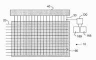
도 1은 본 발명의 실시에 사용될 수 있는 전계발광(EL) 디스플레이의 일실시예의 개략도이다.
도 2는 본 발명의 실시에 사용될 수 있는 EL 서브픽셀의 일실시예의 개략도이다.
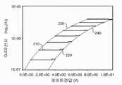
도 3은 2개의 EL 서브픽셀의 특징 차의 디바이스 전류에 대한 영향을 도시한 도표이다.
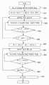
도 4는 본 발명의 방법의 일실예의 블록도이다.
도 5는 픽셀들 간의 특징 차를 나타낸 픽셀 휘도의 히스토그램이다.Figure 1 is a schematic diagram of one embodiment of an electroluminescent (EL) display that may be used in the practice of the present invention.
2 is a schematic diagram of one embodiment of an EL subpixel that may be used in the practice of the present invention.
3 is a chart showing the effect of the feature difference of two EL subpixels on the device current.
4 is a block diagram of one embodiment of a method of the present invention.
FIG. 5 is a histogram of pixel luminance showing characteristic differences between pixels. FIG.
도 1을 참조하면, 본 발명의 실시예에 사용될 수 있는 전계발광(EL) 디스플레이의 일실시예의 개략도가 도시되어 있다. EL 디스플레이(10)는 행렬로 배열된 기설정된 개수의 EL 서브픽셀들(60)의 어레이를 포함한다. 행렬은 도 1에 도시된 것과는 다르게 지향될 수 있음에 유의하라; 예컨대, 행렬은 90도로 회전될 수 있다. EL 디스플레이(10)는 복수의 셀렉트 라인(20)을 포함하고, EL 서브픽셀(60)의 각 행은 셀렉트 라인(20)을 갖는다. EL 디스플레이(10)는 복수의 리드아웃 라인(30)을 포함하고, EL 서브픽셀(60)의 각 열은 리드아웃 라인(30)을 갖는다. 각 리드아웃 라인(30)은 스위치 블록(30)에 연결되어 있고, 스위치 블록은 캘리브레이션 공정동안 리드아웃 라인(30)을 전류소스(160) 또는 전류싱크(165)에 연결시킨다. 도면을 명확히 하기 위해 미도시하였으나, 각 행의 EL 서브픽셀(60)은 또한 해당기술분야에 잘 알려진 데이터 라인을 갖는다. 복수의 리드아웃 라인(30)은 하나 이상의 멀티플렉서(40)에 연결되어 있고, 멀티플렉서는 명백한 바와 같이 EL 서브픽셀(60)로부터 신호의 병렬/순차적 리드아웃을 허용한다. 멀티플렉서(40)는 EL 디스플레이(10)와 동일한 구조의 일부가 될 수 있거나, EL 디스플레이(10)로부터 연결 또는 분리될 수 있는 별도의 구조가 될 수 있다.Referring to Figure 1, a schematic diagram of one embodiment of an electroluminescent (EL) display that may be used in embodiments of the present invention is shown. The
도 2를 참조하면, 본 발명의 실시예에 사용될 수 있는 EL 서브픽셀의 일실시예의 개략도가 도시되어 있다. EL 서브픽셀(60)은 EL 이미터(50), 드라이브 트랜지스터(70), 커패시터(75), 리드아웃 트랜지스터(80), 및 셀렉트 트랜지스터(90)를 포함한다. 각각의 트랜지스터는 제 1 전극, 제 2 전극 및 게이트 전극을 갖는다. 제 1 전압소스(140)가 제 1 스위치(110)에 의해 드라이브 트랜지스터(70)의 제 1 전극에 선택적으로 연결되며, 제 1 스위치는 EL 디스플레이 기판 또는 별도의 구조물에 위치될 수 있다. 연결은 소자들이 직접 연결되거나 또 다른 구성요소, 예컨대, 스위치, 다이오드, 또는 또 다른 트랜지스터를 통해 전기연결되는 것을 의미한다. 드라이브 트랜지스터(70)의 제 2 전극은 EL 이미터(50)에 연결되고, 제 2 전압소스(150)는 제 2 스위치(120)에 의해 EL 이미터(50)에 선택적으로 연결될 수 있으며, 제 2 스위치는 EL 디스플레이 기판에서 떨어져 있을 수 있다. 적어도 하나의 제 1 스위치와 제 2 스위치(120)가 EL 디스플레이용으로 제공된다. EL 디스플레이가 다수의 전력구동 픽셀 서브그루핑을 갖는다면 추가적인 제 1 및 제 2 스위치가 제공될 수 있다. 통상적인 디스플레이 모드에서, 제 1 및 제 2 스위치는 닫히는 반면, (후술된) 다른 스위치들은 개방된다. 드라이브 트랜지스터(70)의 게이트 전극은 트랜지스터(90)를 선택하도록 연결되어 해당기술분야에 잘 알려진 바와 같이 트랜지스터(70)를 구동하도록 데이터 라인(35)으로부터 데이터를 선택적으로 제공한다. 셀렉트 라인(20)은 EL 서브픽셀(60)의 행에 있는 셀렉트 트랜지스터(90)의 게이트 전극에 연결되어 있다. 셀렉트 트랜지스터(90)의 게이트 전극은 리드아웃 트랜지스터(80)의 게이트 전극에 연결되어 있다.Referring to Figure 2, a schematic diagram of one embodiment of an EL subpixel that may be used in an embodiment of the present invention is shown. The
리드아웃 트랜지스터(80)의 제 1 전극은 드라이브 트랜지스터(70)의 제 2 전극과 EL 이미터(50)에 연결되어 있다. 리드아웃 라인(30)은 서브픽셀(60)의 열에 있는 리드아웃 트랜지스터(80)의 제 2 전극에 연결되어 있다. 리드아웃 라인(30)은 스위치 블록(130)에 연결되어 있다. 한 스위치 블록(130)은 EL 서브픽셀(60)의 각 열에 제공된다. 스위치 블록(130)은 제 3 스위치(S3)와 제 4 스위치(S4), 및 노컨넥트 상태(NC)를 포함한다. 제 3 및 제 4 스위치가 각각의 엔티티일 수 있는 반면, 상기 스위치들은 결코 동시에 이런 식으로 닫히지 않으므로, 스위치 블록(130)은 2개 스위치들의 편리한 실시예를 제공한다. 제 3 스위치는 전류소스(160)가 리드아웃 트랜지스터(80)의 제 2 전극에 선택적으로 연결되게 한다. 제 3 스위치에 의한 연결시 전류소스(160)는 기설정된 일정 전류가 EL 서브픽셀(60)로 흐르게 한다. 제 4 스위치는 전류싱크(165)가 리드아웃 트랜지스터(80)의 제 2 전극에 선택적으로 연결되게 한다. 제 4 스위치에 의한 연결시, 전류싱크(165)는 기설정된 데이터 값이 데이터 라인(35)에 가해지면 기설정된 일정 전류가 EL 서브픽셀(60)로 흐르게 한다. 스위치 블록(130), 전류소스(160) 및 전류싱크(165)는 EL 디스플레이 기판상에 또는 밖에 위치될 수 있다.The first electrode of the
복수의 EL 서브픽셀을 포함한 EL 디스플레이에서, 단일 전류소스와 전류싱크가 각각 제 3 및 제 4 스위치를 통해 복수의 EL 서브픽셀에 있는 각각의 리드아웃 트랜지스터의 제 2 전극에 선택적으로 연결된다. 리드아웃 트랜지스터의 제 2 전극이 어떤 소정의 순간에 선택적으로 하나의 전류소스 또는 하나의 전류싱크에 선택적으로 연결되거나 어디에도 연결되지 않는다면, 하나 이상의 전류소스 또는 전류싱크가 이용될 수 있다.In an EL display including a plurality of EL subpixels, a single current source and a current sink are selectively connected to the second electrode of each of the lead-out transistors in the plurality of EL subpixels through the third and fourth switches, respectively. At least one current source or current sink may be used if the second electrode of the lead-out transistor is selectively connected to one current source or one current sink, or not connected anywhere, at any given moment.
리드아웃 트랜지스터(80)의 제 2 전극은 또한 전압측정회로(170)에 연결되며, 상기 회로는 전압을 측정해 EL 서브픽셀(60)의 특징을 나타내는 신호를 제공한다. 전압측정회로(170)는 전압 측정을 디지털신호로 변환하는 아날로그-디지털 컨버터(185)와 프로세서(190)를 포함한다. 아날로그-디지털 변환기(185)로부터의 신호가 프로세서(190)로 보내진다. 전압측정회로(170)는 또한 전압측정을 저장하기 위한 메모리(195)와 필요하다면 저역통과필터(180)를 포함할 수 있다. 전압측정회로(170)는 멀티플렉서 출력라인(45)과 멀티플렉서(40)를 통해 EL 서브픽셀(60)의 기설정된 개수로부터 전압을 순차적으로 판독하기 위한 복수의 리드아웃 라인(30)과 리드아웃 트랜지스터(80)에 연결될 수 있다. 복수의 멀티플렉서(40)가 있다면, 각각은 자신의 멀티플렉서 출력라인(45)을 가질 수 있다. 따라서, 기설정된 개수의 EL 서브픽셀(60)이 동시에 구동될 수 있다. 복수의 멀티플렉서(40)는 다양한 멀티플렉서(40)로부터 전압의 병렬식 리드아웃을 허용하는 반면, 각 멀티플렉서(40)는 부착된 리드아웃 라인(30)의 순차적 리드아웃을 허용한다. 이를 본 명세서에서 병렬/순차 프로세스라 한다.The second electrode of the lead-
프로세서(190)는 또한 컨트롤 라인(95)과 디지털-아날로그 컨버터(155)에 의해 데이터 라인(35)에 연결될 수 있다. 따라서, 프로세서(190)는 본 명세서에 기술된 측정 프로세스 동안 데이터 라인(35)에 기설정된 데이터 값을 제공할 수 있다. 프로세서(190)는 또한 85의 데이터를 통해 디스플레이 데이터를 수용할 수 있고 본 명세서에 상술한 바와 같이 변화에 대한 보상을 제공할 수 있어, 디스플레이 프로세스 동안 데이터 라인(35)에 보상된 데이터를 제공할 수 있다.The
도 1에 도시된 실시예는 비역전 NMOS 서브픽셀이다. 해당기술분야에 공지된 다른 형태가 본 발명에 이용될 수 있다. 각 트랜지스터(70,80,90)는 N채널 또는 P채널일 수 있고, EL 이미터(50)는 역전 또는 비역전 배열로 드라이브 트랜지스터(70)에 연결될 수 있다. EL 이미터(50)는 탕 등(Tang et al.)의 미국특허 No. 4,769,292 및 반슬리케 등(VanSlyke et al.)의 미국특허 No. 5,061,569에 개시되었으나 이에 국한되지 않는 유기발광 다이오드(OLED) 이미터 또는 해당기술분야에 공지된 다른 이미터 타입일 수 있다. EL 이미터(50)가 OLED 이미터이면, EL 서브픽셀(60)은 OLED 서브픽셀이고, EL 디스플레이(10)는 OLED 디스플레이이다. 드라이브 트랜지스터(70)와 다른 트랜지스터(80,90)는 저온 폴리실리콘(LTPS), 아연산화물(ZnO), 또는 비정질 실리콘(a-Si) 트랜지스터일 수 있거나 해당기술분야에 공지된 또 다른 타입의 트랜지스터이다.The embodiment shown in Figure 1 is a non-inverting NMOS subpixel. Other forms known in the art may be used in the present invention. Each
EL 서브픽셀(60)의 드라이브 트랜지스터(70)와 같은 트랜지스터는 임계전압(Vth) 및 이동도(μ)를 포함한 특징을 갖는다. 드라이브 트랜지스터(70)의 게이트 전극에 대한 전압은 제 1 및 제 2 전극 간에 큰 전류 흐름을 가능하게 하도록 임계전압보다 더 커야 한다. 이동도는 트랜지스터가 도전될 때 전류량에 관계 있다. 저온 폴리실리콘(LTPS)의 트랜지스터 뒷면과 함께 디스플레이 사용시, 디스플레이내 모든 트랜지스터들이 동일한 임계전압(Vth) 또는 이동도 값을 가질 필요는 없다. EL 서브픽셀(60)에서 다양한 드라이브 트랜지스터들의 특징들 간에 차이로 인해 모든 드라이브 트랜지스터들이 동일한 게이트-소스 전압(Vgs)에 의해 구동될 때 디스플레이의 표면에 걸쳐 출력된 광이 시각적으로 불균일해 질 수 있다. 이런 불균일성은 디스플레이의 다른 부분에서 휘도와 컬러 밸런스의 차이를 포함할 수 있다. 이런 문제를 방지하기 위해 임계전압 및 이동도에서 이런 차이를 보상하는 것이 바람직하다. 또한, 효율 또는 저항과 같은 EL 이미터(50)의 특징에서 차이가 있을 수 있어, 또한 시각적 불균일성을 야기할 수 있다.Transistors such as
본 발명은 임의의 소정 시간에서 특징 및 결과적으로 발생한 불균일성에서 차이를 보상할 수 있다. 그러나, 불균일성은 특히 최초로 디스플레이를 보는 최종 사용자에게 불쾌할 수 있다. EL 디스플레이의 동작수명은 최종사용자가 디스플레이 상에 이미지를 최초로 볼 때의 시간으로부터 디스플레이가 폐기되는 시간까지이다. 초기 불균일성은 디스플레이의 동작수명의 시작시에 있는 임의의 불균일성이다. 본 발명은 EL 디스플레이의 동작수명이 시작되기 전에 측정을 함으로써 초기 불균일성을 이점적으로 보상할 수 있다. 측정은 디스플레이 생산의 일부로서 공장에서 행해질 수 있다. 측정은 또한 디스플레이에 첫 이미지가 나타나기 전에 EL 디스플레이를 포함한 제품을 최초로 작동시킨 후 취해질 수 있다. 이는 최종사용자가 먼저 볼때 디스플레이가 고품질의 이미지를 최종사용자에게 나타내게 하므로, 디스플레이의 첫인상이 마음에 들게 된다.The present invention can compensate for differences in the non-uniformities that occur in character and consequently at any given time. However, non-uniformity can be particularly uncomfortable to the end-user viewing the display for the first time. The operating lifetime of the EL display is from the time when the end user first views the image on the display to the time the display is discarded. The initial non-uniformity is any non-uniformity at the beginning of the operational life of the display. The present invention can advantageously compensate for the initial non-uniformity by making measurements before the operating life of the EL display begins. Measurements can be made at the factory as part of display production. Measurements can also be taken after the first operation of the product, including the EL display, before the first image appears on the display. This allows the display to display a high quality image to the end user when viewed first by the end user, so that the first impression of the display is appreciated.
도 3을 참조하면, 또는 EL 서브픽셀 전류에 대한 2개의 EL 이미터 또는 드라이브 트랜지스터, 또는 모두의 특징에 있어 차이의 영향을 나타낸 도표가 도시되어 있다. 도 3의 가로좌표는 드라이브 트랜지스터(70)에서 게이트 전압을 나타낸다. 세로좌표는 EL 이미터(50)를 통과한 전류의 10을 밑으로 한 로그이다. 제 1 EL 서브픽셀(I-V) 특징(230)과 제 2 EL 서브픽셀(I-V) 특징(240)은 2개의 다른 EL 서브픽셀(60)에 대한 I-V 곡선을 나타낸다. 바람직한 전류를 얻기 위해 특징(230)보다 더 큰 전압이 특징(240)에 요구된다; 즉, 곡선은 양(ΔV)만큼 오른쪽으로 이동되어 있다. ΔV는 도시된 바와 같이 임계전압(ΔVth, 210)의 변화와 EL 이미터 저항(ΔVEL, 220)의 변화로부터 발생한 EL 전압의 변화의 합이다. 이 변화로 특징(230 및 240)을 각각 갖는 서브픽셀들 간에 광 방출이 불균일해진다: 주어진 게이트 전압은 전류를 잘 제어하지 못하므로 특징(230)보다 특징(240)에서 밝기가 떨어진다.Referring to FIG. 3, there is shown a diagram illustrating the effect of differences in the characteristics of two EL emitters or drive transistors, or both, for an EL sub-pixel current. The abscissa of FIG. 3 represents the gate voltage at the
EL 전류(또한 드라이브 트랜지스터를 통하는 드레인-소스 전류), EL 전압 및 임계전압 간의 관계는 다음과 같다:The relationship between the EL current (also the drain-source current through the drive transistor), the EL voltage and the threshold voltage is as follows:

여기서, W는 TFT 채널폭이고, L은 TFT 채널길이이며, μ는 TFT 이동도이고, C0는 단위면적당 산화물 커패시턴스이며, Vg는 게이트 전압이고, Vg3는 드라이브 트랜지스터의 게이트와 소스 간의 전압차이다. 간략히 하기 위해, Vg3에 대한 μ의 의존성을 무시한다. 따라서, 특징(230 및 240)을 갖는 서브픽셀로부터 동일한 전류를 만들기 위해, Vth 및 VEL의 차를 보상해야 한다. 따라서 모든 변화를 측정하는 것이 바람직하다.Here, W is the TFT Channel Width, L is the TFT Channel Length, μ is a TFT mobility is, C0 is a per unit area of the oxide capacitance, Vg is the gate voltage, Vg3 is the voltage between the gate and the source of the drive transistor It's a car. For the sake of simplicity, the dependence of μ on Vg3 is neglected. Thus, to make the same current from subpixels with
도 4와 또한 도 2를 참조하면, 본 발명의 방법의 일실시예의 블록도가 도시되어 있다. 기설정된 테스트 전압(Vdata)이 데이터 라인(35)에 제공된다(단계 310). 제 1 스위치(110)가 닫히고 제 2 스위치(120)가 열린다. 제 4 스위치가 닫히고 제 3 스위치가 열린다. 즉, 스위치 블록(130)이 S4로 전환된다(단계 315). 셀렉트 라인(20)은 선택된 행에 대해 활성화되어 테스트 전압을 드라이브 트랜지스터(70)의 게이트 전극에 제공하고 선택된 EL 서브픽셀에 있는 리드아웃 트랜지스터(80)를 온시킨다(단계 320). 이는 선택된 EL 픽셀의 드라이브 트랜지스터, 리드아웃 트랜지스터 및 EL 이미터를 선택한다. 따라서 전류는 제 1 전압소스(140)로부터 드라이브 트랜지스터(70)를 통해 전류싱크(165)로 흐른다. Vdata의 인가로 인해 드라이브 트랜지스터(70)를 통해 최종 발생한 전류 미만이 되도록 전류싱크(165)를 통한 전류(Itestsk) 값이 선택된다; 일반적인 값은 1 내지 5 마이크로암페어 범위이며 특정한 특정세트에서 취해진 모든 측정들에 대해 일정하다. 선택된 Vdata 값은 모든 이런 측정에 대해 일정하고 따라서 심지어 디스플레이의 수명 동안 예상된 노화 후에도 전류싱크(165)에서의 전류보다 더 큰 드라이브 트랜지스터(70)를 지나는 전류를 명령할 정도로 충분해야 한다. 그러므로, 드라이브 트랜지스터(70)를 통과한 전류의 제한 값은 전류싱크(165)에 의해 완전히 제어되며, 이는 드라이브 트랜지스터(70)를 통해 동일하다. Vdata 값은 기지의 또는 기설정된 전류-전압 및 드라이브 트랜지스터(70)의 노화 특징을 바탕으로 선택될 수 있다. 이 과정에서 하나 이상의 측정값이 사용될 수 있다. 예컨대, 1, 2, 및 3 마이크로암페어로 측정을 하도록 선택될 수 있다. 가장 큰 테스트 전류보다 적지 않은 전류를 명령하기에 충분한 Vdata 값이 사용되어야 한다. 전압측정회로(170)는 이는 선택된 리드아웃 트랜지스터(80)의 제 2 전극에서의 전압(Vout)인 리드아웃 라인(30)상에 전압을 측정하는데 사용되며, 드라이브 트랜지스터(70)의 임계전압(Vth)을 포함해 선택된 드라이브 트랜지스터(70)의 특징을 나타내는 해당하는 제 1 신호(V1)를 제공한다(단계 325). EL 디스플레이가 복수의 EL 서브픽셀을 포함하고 측정된 행에서 추가 EL 서브픽셀들이 있으면, 복수의 리드아웃 라인(30)에 연결된 멀티플렉서(40)는 전압측정회로(170)가 기설정된 개수의 EL 서브픽셀들, 예컨대, 행에서 있는 모든 서브픽셀들로부터 제 1 신호(V1)를 순차적으로 리드아웃하도록 사용될 수 있다(단계 330). 디스플레이가 충분히 크면, 복수의 멀티플렉서들을 필요로 할 수 있고, 제 1 신호가 병렬/순차 프로세스에 제공될 수 있다. 피측정 서브픽셀들의 행들이 추가로 있으면(단계 335), 다른 셀렉트 라인에 의해 다른 행이 선택되고, 측정이 반복된다.Referring to Figure 4 and also Figure 2, a block diagram of one embodiment of the method of the present invention is shown. A predetermined test voltage (Vdata ) is provided to the data line 35 (step 310). The
각 서브픽셀에서 보상 전압은 아래에 의해 관계될 수 있다The compensation voltage at each subpixel can be related by

여기서 Vgs(Itestsk)는 드레인-소스 전류(Ids)가 Itestsk와 같도록 트랜지스터(70)를 구동시기 위해 인가되어야 하는 게이트-소스 전압이다. 이 전압 값은 리드아웃 트랜지스터(80)의 제 2 전극에서의 전압(V1을 제공하도록 읽혀지는 Vout)이 수학식 2를 충족하도록 조절되게 한다. 상술한 조건 하에서, Vdata는 세트 값이고 Vread는 일정한 것으로 가정할 수 있다. Vgs는 전류싱크(165)에 의해 설정된 전류 값과 드라이브 트랜지스터(70)의 전류-전압 특징에 의해 제어되고, 드라이브 트랜지스터의 임계전압의 다른 값들에 대해서 다르다. 이동도 변화를 보상하기 위해, V1의 2개 값들이 다른 Itestsk 값에서 취해져야 한다.Here, Vgs(Itestsk) is the drain-source voltage - gate to source current (Ids) is to be applied to the
전류싱크(165)에 대해 선택된 값들에 따라 각 서브픽셀에 대해 첫신호(V1) 값이 기록될 수 있다. 그런 후, 최대 V1(이와 같이, 최소 Vgs(Itestsk) 및 그러한 최소 Vth)을 갖는 서브픽셀이 측정된 서브픽셀의 모집단으로부터 제 1 타겟신호(V1target)로서 선택된다. 대안으로, 모든 V1 값들의 최소 또는 평균 또는 당업자에 명백한 다른 함수들의 결과들이 V1target으로서 선택될 수 있다. 그런 후, 각 서브픽셀에 대해 측정된 제 1 신호 V1는 첫 타겟 신호 V1target와 비교되어 각 서브픽셀에 대해 다음과 같이 델타 ΔV1을 형성할 수 있다:The value of the first signal (V1 ) may be written for each subpixel according to the values selected for the

ΔV1은 각 서브픽셀과 타겟 사이에 임계전압 차를 나타낸다.ΔV1 represents a threshold voltage difference between each subpixel and the target.
본 발명은 하나의 EL 서브픽셀은 비교할 게 없으면 특징에서 전혀 차이가 없기 때문에 복수의 EL 서브픽셀에만 적용되는 것에 유의하라. 즉, 하나의 EL 서브픽셀, V1=V1target에 대해, ΔV1은 항상 0이다.Note that the present invention is applied to only a plurality of EL subpixels since there is no difference in characteristics when one EL subpixel is not compared. That is, for one EL subpixel, V1 = V1target,? V1 is always zero.
EL 이미터를 측정하기 위해 도 4를 다시 참조하면, 제 1 스위치(110)가 열리고 제 2 스위치(120)가 닫힌다. 스위치 블록(130)이 S3로 전환됨으로써, 제 4 스위치가 열리고 제 3 스위치는 닫힌다(단계 340). 셀렉트 라인(20)은 셀렉트 행을 활성화시켜 리드아웃 트랜지스터(70)를 온시킨다(단계 345). 전류 Itestsu가 이에 따라 전류 소스(160)로부터 EL 이미터(50)를 통해 제 2 전압소스(150)로 흐른다. 전류 소스(160)를 통한 전류 값은 EL 이미터(50)를 지나는 가능한 최대 전류보다 적게 선택된다; 일반적인 값은 1에서 5 마이크로암페어 범위에 있고 특별한 측정 세트로 취한 모든 측정들에 대해 일정하다. 하나 이상의 측정값이 이 과정에서 사용될 수 있다. 예컨대, 1, 2, 및 3 마이크로암페어로 측정하도록 선택할 수 있다. 전압측정회로(170)가 리드아웃라인(30)을 측정하는데 사용될 수 있고, 리드아웃라인은 선택된 리드아웃 트랜지스터(80)의 제 2 전극에서 전압 Vout이며, 선택된 EL 이미터(50)의 특징을 나타내는 제 2 신호 V2를 제공한다(단계 350). 피측정 행에서 추가 EL 서브픽셀이 있으면, 복수의 리드아웃 라인(30)에 연결된 멀티플렉서(40)가 사용될 수 있어 전압측정회로(70)가 기설정된 EL 서브픽셀, 예컨대, 행에 있는 모든 서브픽셀에 대해, 순차적으로 제 2 신호(V2)를 리드아웃하게 한다(단계 355). 디스플레이가 충분히 크면, 복수의 멀티플렉서들을 필요로 할 수 있고, 제 2 신호가 병렬/순차 프로세스로 제공될 수 있다. EL 디스플레이(10)에서 측정될 추가 서브픽셀 행이 있으면, 단계(345 내지 355)가 각 행에 대해 반복된다(단계 360).Referring again to FIG. 4 for measuring the EL emitter, the
각 서브픽셀에서 구성요소들의 전압은 다음에 의해 연관될 수 있다:The voltage of the components in each subpixel can be related by:

이들 전압 값으로 인해 리드아웃 트랜지스터(80)의 제 2 전극에서 전압이 수학식 4를 이행하도록 조절된다. 상술한 조건 하에서, CV는 설정 값이고 Vread는 상수로 가정될 수 있다. VEL은 전류소스(160)와 EL 이미터(50)의 전류 전압특징에 의해 설정된 전류값으로 제어된다. VEL은 다른 EL 이미터들(50)에 대해 달라질 수 있다.Due to these voltage values, the voltage at the second electrode of the
제 2 신호(V2) 값은 각각 서브픽셀들에 대해 전류소스(60)에 대해 설정된 값들로 기록될 수 있다. 그런 후, 최소 VEL을 갖는 서브픽셀(즉, 측정된 최소 V2)이 측정된 서브픽셀의 모집단으로부터 제 2 타겟 신호(V2target)로서 선택된다. 대안으로, 모든 V2 값의 최대 또는 평균 또는 당업자에 명백한 다른 함수의 결과들이 V2target으로서 선택될 수 있다. 그런 후, 각 서브픽셀에 대해 측정된 제 2 신호(V2)는 다음과 같이 델타 ΔV2를 이루도록 제 2 타겟신호(V2target)와 비교할 수 있다:The value of the second signal (V2 ) may be written with the values set for the

ΔV2는 각 서브픽셀과 타겟 간에 EL 이미터 전압의 차를 나타낸다.ΔV2 represents the difference between the EL emitter voltage between each subpixel and the target.
복수의 EL 서브픽셀에서 각 EL 서브픽셀 측정시, 도 4에 도시된 바와 같이, 제 1 신호가 모든 EL 서브픽셀에 대해 판독되고 그런 후 제 2 신호가 모든 EL 서브픽셀에 대해 판독될 수 있다. 그러나, 측정은 인터리브될 수 있다. 제 1 및 제 2 신호가 복수의 EL 서브픽셀들에 있는 모든 EL 서브픽셀들에 대해 판독될 때까지, 제 1 신호가 제 1 EL 서브픽셀로부터 판독되고 그런 후 제 2 신호가 제 1 EL 서브픽셀에 대해 판독되며, 제 2 신호가 제 2 EL 서브픽셀로부터 판독되고, 그런 후 제 2 신호가 제 2 EL 서브픽셀에 대해 등등 판독될 수 있다.During each EL subpixel measurement in a plurality of EL subpixels, a first signal can be read for all EL subpixels and then a second signal can be read for all EL subpixels, as shown in FIG. However, the measurements can be interleaved. The first signal is read from the first EL subpixel and then the second signal is read from the first EL subpixel until the first and second signals are read for all the EL subpixels in the plurality of EL subpixels, And the second signal is read out from the second EL subpixel, and then the second signal can be read out for the second EL subpixel and so on.
각 EL 서브픽셀의 제 1 및 제 2 신호에서 델타 ΔV1 및 ΔV2는 각각 EL 디스플레이와 같은 복수의 EL 서브픽셀에서 다른 EL 서브픽셀(60)의 특징 차를 보상하는데 사용될 수 있다(단계 370). 다수의 서브픽셀들 간의 전류 차를 보상하기 위해, (ΔV1과 관련된)ΔVth 및 (ΔV2와 관련된)ΔVEL에 대한 교정을 하는게 필요하다.In the first and second signal of each EL sub-pixel delta ΔV1 and ΔV2 may be used to compensate for the characteristic difference of the other EL sub-pixels 60 in a plurality of EL subpixels, such as each of the EL display (step 370) . In order to compensate a current difference between a plurality of subpixels, it would need to calibration for ΔVEL (related to ΔV2) ΔVth and (related to ΔV1).
EL 서브픽셀(60)의 특징 차를 보상하기 위해, 다음 형태의 수식에서 제 1 및 제 2 신호의 델타를 사용할 수 있다:To compensate for the feature difference of the

여기서 ΔVdata는 선택된 Vdata에 의해 특징된 소정의 휘도를 유지하는데 필요한 드라이브 트랜지스터(70)의 게이트 전극에 대한 오프세트 전압이고, f1(ΔV1)은 임계전압 차에 대한 보상이며, f2(ΔV2)는 EL 저항의 차에 대한 보상이다. ΔV1은 수학식 3에 주어져 있고, ΔV2는 수학식 5에 주어져 있다. 예컨대, EL 디스플레이는 컨트롤러를 포함할 수 있어, 각 EL 이미터에 대한 오프세트 전압을 계산하기 위한 참조표 또는 알고리즘을 포함할 수 있다. 예컨대, f1은 드라이브 트랜지스터의 Ids가 Vgs-Vth에 의해 결정되므로 소정의 Vth 변화 ΔV1가 같은 양만큼 (대략 Vg와 같은) Vdata를 변경함으로써 보상될 수 있기 때문에 선형함수일 수 있다. 구동 트랜지스터의 제 2 단자에 연결된 EL 이미터를 갖는 실시예에서, f2는 또한 유사한 이유로 선형함수일 수 있다: 전압 소스의 변경은 같은 양만큼 Vgs를 변경한다. 더 복잡한 경우, 시스템은 SPICE 시뮬레이션과 같이 당업자에 알려진 기술에 의해 모델화될 수 있고, f1 및 f2는 사전계산된 값의 참조표로서 구현될 수 있다. 이동도 변화를 보상하기 위해, 다른 Itestsk 값에서 2개의 측정된 V1 값이 모든 서브픽셀의 I-V 곡선의 평균, 최소, 또는 최대로서 선택된 기준 I-V 곡선상에 각 서브픽셀에 대해 I-V 곡선을 맵핑하는 오프세트와 이득을 결정하기 위해 사용될 수 있다. 오프세트와 이득은 기준 곡선상의 Vdata를 변환 곡선상의 같은 전압으로 변환하는데 사용될 수 있다. 이 선형변환은 Vth와 이동도 차를 동시에 고려할 수 있다.Where ΔVdata is the offset voltage for the gate electrode of the
오프세트 전압 ΔVdata은 드라이드 트랜지스터(70)의 임계전압과 이동도 및 EL 이미터(50)의 저항의 차로 인한 전류 차의 교정을 제공하도록 계산된다. 이는 완전한 보상 방식을 제공한다. 이들 변화는 출력광을 소정의 공칭 휘도값으로 교정하기 위해 콘트롤러에 적용될 수 있다. EL 이미터에 인가된 신호를 제어함으로써, 일정한 출력 휘도와 소정 휘도에서 증가된 수명을 갖는 EL 이미터가 달성된다. 이 방법은 디스플레이에서 각 EL 이미터에 대한 교정을 제공하기 때문에, 복수의 EL 서브픽셀의 특징 차를 보상하고 따라서 복수의 EL 서브픽셀을 갖는 EL 디스플레이의 초기 비균일성을 보상할 수 있다.The offset voltage? Vdata is calculated to provide correction of the difference in current due to the difference between the threshold voltage and the mobility of the
10 EL 디스플레이
20 셀렉트 라인
30 리드아웃 라인
35 데이터 라인
40 멀티플렉서
45 멀티플렉서 출력라인
50 EL 이미터
60 EL 서브픽셀
70 드라이브 트랜지스터
75 커패시터
80 리드아웃 트랜지스터
85 데이터 인
90 셀렉트 트랜지스터
95 컨트롤 라인
110 제 1 스위치
120 제 2 스위치
130 스위치 블록
140 제 1 전압소스
150 제 2 전압소스
155 디지털-아날로그 컨버터
160 전류소스
165 전류싱크
170 전압측정회로
180 저역통과필터
185 아날로그-디지털 컨버터
190 프로세서
195 메모리
210 ΔVth
220 ΔVEL
230 제 1 EL 서브필셀 I-V 특징
240 제 2 EL 서브필셀 I-V 특징
310 단계
315 단계
320 단계
325 단계
330 단계
335 단계
340 단계
350 단계
355 결정단계
360 결정단계
370 단계10 EL display
20 Select Line
30 lead out line
35 data lines
40 multiplexer
45 Multiplexer Output Lines
50 EL emitter
60 EL subpixel
70 drive transistor
75 capacitors
80 lead-out transistor
85 data in
90 select transistor
95 control lines
110 first switch
120 second switch
130 switch block
140 first voltage source
150 second voltage source
155 digital to analog converters
160 Current Source
165 Current sink
170 voltage measurement circuit
180 low-pass filter
185 Analog to Digital Converters
190 Processor
195 Memory
210 ΔVth
220 ΔVEL
230 1st EL Sub-Fill Cell IV Features
240 2nd EL Sub-Fill Cell IV Features
355 determination step
360 decision step
Claims (11)
Translated fromKorean(b) 제 1 전압소스를 각 드라이브 트랜지스터의 제 1 전극에 선택적으로 연결하기 위해 제 1 전압소스와 제 1 스위치를 제공하는 단계와,
(c) 각각의 드라이브 트랜지스터의 제 2 전극에 연결된 각 EL 서브픽셀에 EL 이미터를 제공하고, 각 EL 이미터를 제 2 전압소스에 선택적으로 연결시키기 위해 제 2 전압소스 및 제 2 스위치를 제공하는 단계와,
(d) 제 1 전극과 제 2 전극을 갖는 리드아웃 트랜지스터를 각 EL 서브픽셀에 제공하고 각각의 리드아웃 트랜지스터의 제 1 전극을 각각의 드라이브 트랜지스터의 제 2 전극에 연결하는 단계와,
(e) 전류소스를 각 리드아웃 트랜지스터의 제 2 전극에 선택적으로 연결하기 위해 전류소스와 제 3 스위치를 제공하는 단계와,
(f) 전류싱크를 각 리드아웃 트랜지스터의 제 2 전극에 선택적으로 연결하기 위해 전류싱크와 제 4 스위치를 제공하는 단계와,
(g) EL 서브픽셀과 해당 드라이브 트랜지스터, 리드아웃 트랜지스터 및 EL 이미터를 선택하는 단계와,
(h) 선택된 드라이브 트랜지스터의 게이트 전극에 테스트 전압을 제공하고, 선택된 리드아웃 트랜지스터의 제 2 전극에 연결된 전압측정회로를 제공하는 단계와,
(i) 제 1 및 제 4 스위치를 닫고 제 2 및 제 3 스위치를 열어, 전압측정회로를 이용해 선택된 리드아웃 트랜지스터의 제 2 전극에서의 전압을 측정하여 선택된 드라이브 트랜지스터의 특징을 나타내는 대응하는 제 1 신호를 제공하는 단계와,
(j) 제 1 및 제 4 스위치를 열고 제 2 및 제 3 스위치를 닫아, 전압측정회로를 이용해 선택된 리드아웃 트랜지스터의 제 2 전극에서의 전압을 측정하여 선택된 EL 이미터의 특징을 나타내는 대응하는 제 2 신호를 제공하는 단계와,
(k) 복수의 EL 서브픽셀에서 각각의 남아 있는 EL 서브픽셀에 대해 단계 g 내지 j를 반복하는 단계와,
(l) 복수의 EL 서브픽셀의 특징 차를 보상하기 위해 각 서브픽셀에 대한 제 1 및 제 2 신호를 이용하는 단계를 포함하는 복수의 전계발광(EL) 서브픽셀의 특징 차를 보상하는 방법.(a) providing a drive transistor having a first electrode, a second electrode, and a gate electrode to each of a plurality of EL subpixels,
(b) providing a first voltage source and a first switch to selectively connect a first voltage source to a first electrode of each drive transistor,
(c) providing an EL emitter for each EL sub-pixel coupled to a second electrode of each drive transistor, and providing a second voltage source and a second switch for selectively coupling each EL emitter to a second voltage source , ≪ / RTI &
(d) providing a lead-out transistor having a first electrode and a second electrode to each EL sub-pixel and connecting a first electrode of each lead-out transistor to a second electrode of each drive transistor,
(e) providing a current source and a third switch to selectively connect a current source to a second electrode of each lead-out transistor,
(f) providing a current sink and a fourth switch to selectively connect a current sink to a second electrode of each lead-out transistor,
(g) selecting the EL sub-pixel and the drive transistor, the lead-out transistor and the EL emitter,
(h) providing a test voltage to a gate electrode of a selected drive transistor and providing a voltage measurement circuit coupled to a second electrode of the selected lead-out transistor,
(i) closing the first and fourth switches and opening the second and third switches, measuring the voltage at the second electrode of the selected lead-out transistor using the voltage measurement circuit to determine the corresponding first Providing a signal,
(j) opening the first and fourth switches, closing the second and third switches, measuring the voltage at the second electrode of the selected lead-out transistor using the voltage measurement circuit, 2 signal,
(k) repeating steps g to j for each remaining EL subpixel in the plurality of EL subpixels,
(l) using first and second signals for each subpixel to compensate for a feature difference of a plurality of EL subpixels.
전압측정회로는 선택된 리드아웃 트랜지스터의 제 2 전극에서의 측정된 전압을 디지털 신호로 변환하는 아날로그-디지털 컨버터를 포함하는 복수의 전계발광(EL) 서브픽셀의 특징 차를 보상하는 방법.The method according to claim 1,
A voltage measurement circuit includes an analog-to-digital converter for converting a measured voltage at a second electrode of a selected lead-out transistor into a digital signal.
전압측정회로는 상기 디지털 신호를 필터링하는 저역통과필터를 더 포함하는 복수의 전계발광(EL) 서브픽셀의 특징 차를 보상하는 방법.3. The method of claim 2,
Wherein the voltage measurement circuit further comprises a low-pass filter for filtering the digital signal.
단계 g 내지 j는 기설정된 개수의 EL 서브픽셀들이 동시에 구동되는 동안 EL 서브픽셀의 기설정된 개수에 대하여 수행되는 복수의 전계발광(EL) 서브픽셀의 특징 차를 보상하는 방법.The method according to claim 1,
Wherein steps g to j compensate for a feature difference of a plurality of electroluminescent (EL) subpixels performed for a predetermined number of EL subpixels while a predetermined number of EL subpixels are simultaneously driven.
단계 j는 EL 서브픽셀의 특징 차를 보상하기 위해 각각의 복수의 EL 서브픽셀에 대해 측정된 제 1 및 제 2 신호를 제 1 및 제 2 타겟신호 각각과 비교하는 단계를 포함하는 복수의 전계발광(EL) 서브픽셀의 특징 차를 보상하는 방법.The method according to claim 1,
Step j comprises comparing the first and second signals measured for each of the plurality of EL subpixels with each of the first and second target signals to compensate for the feature difference of the EL subpixels, (EL) subpixel.
EL 서브픽셀은 행렬로 배열되고,
단계 f 이후, 행에서 셀렉트 트랜지스터의 게이트 전극에 연결된 셀렉트 라인을 각 행에 그리고, 열에서 리드아웃 트랜지스터의 제 2 전극에 연결된 리드아웃 라인을 각 열에 제공하는 단계를 더 포함하는 복수의 전계발광(EL) 서브픽셀의 특징 차를 보상하는 방법.The method according to claim 1,
EL subpixels are arranged in a matrix,
Further comprising the step of providing in each column a lead-out line connected to the gate electrode of the select transistor in each row, and a lead-out line connected in series to the second electrode of the lead-out transistor, EL) subpixel.
단계 l 이후, 기설정된 개수의 EL 서브픽셀에 대해 제 1 및 제 2 신호를 순차적으로 리드아웃하기 위해 복수의 리드아웃 라인에 연결된 멀티플렉서를 이용하는 단계를 더 포함하는 복수의 전계발광(EL) 서브픽셀의 특징 차를 보상하는 방법.The method according to claim 6,
Further comprising using a multiplexer coupled to the plurality of lead-out lines to sequentially lead out the first and second signals for a predetermined number of EL subpixels after step l, The method comprising:
단계 c 이후, 드라이브 트랜지스터의 게이트 전극에 연결된 셀렉트 트랜지스터를 제공하는 단계를 더 포함하고, 셀렉트 트랜지스터의 게이트 전극은 리드아웃 트랜지스터의 게이트 전극에 연결되는 복수의 전계발광(EL) 서브픽셀의 특징 차를 보상하는 방법.The method according to claim 1,
Further comprising the step of providing a select transistor connected to the gate electrode of the drive transistor after step c, wherein the gate electrode of the select transistor has a feature difference of a plurality of electroluminescent (EL) subpixels connected to the gate electrode of the readout transistor How to compensate.
각 EL 이미터는 OLED 이미터이고, 각 EL 서브픽셀은 OLED 서브픽셀인 복수의 전계발광(EL) 서브픽셀의 특징 차를 보상하는 방법.The method according to claim 1,
Each EL emitter is an OLED emitter, and each EL sub-pixel is an OLED sub-pixel.
각 드라이브 트랜지스터는 저온 폴리실리콘 드라이브 트랜지스터인 복수의 전계발광(EL) 서브픽셀의 특징 차를 보상하는 방법.The method according to claim 1,
Wherein each drive transistor is a low temperature polysilicon driver transistor.
복수의 EL 서브픽셀은 EL 디스플레이를 포함하고, EL 디스플레이의 동작수명 전에 단계 g 내지 k의 측정이 취해지는 복수의 전계발광(EL) 서브픽셀의 특징 차를 보상하는 방법.The method according to claim 1,
Wherein the plurality of EL subpixels comprise an EL display and the measurements of steps g through k are taken before the operating lifetime of the EL display.
Applications Claiming Priority (2)
| Application Number | Priority Date | Filing Date | Title |
|---|---|---|---|
| US12/258,388 | 2008-10-25 | ||
| US12/258,388US8299983B2 (en) | 2008-10-25 | 2008-10-25 | Electroluminescent display with initial nonuniformity compensation |
Publications (2)
| Publication Number | Publication Date |
|---|---|
| KR20110074986A KR20110074986A (en) | 2011-07-05 |
| KR101610040B1true KR101610040B1 (en) | 2016-04-07 |
Family
ID=41503566
Family Applications (1)
| Application Number | Title | Priority Date | Filing Date |
|---|---|---|---|
| KR1020117008892AActiveKR101610040B1 (en) | 2008-10-25 | 2009-10-21 | Electroluminescent Display with Initial Nonuniformity Compensation |
Country Status (7)
| Country | Link |
|---|---|
| US (1) | US8299983B2 (en) |
| EP (1) | EP2351009A1 (en) |
| JP (1) | JP2012507041A (en) |
| KR (1) | KR101610040B1 (en) |
| CN (1) | CN102203846B (en) |
| TW (1) | TWI449017B (en) |
| WO (1) | WO2010047791A1 (en) |
Families Citing this family (28)
| Publication number | Priority date | Publication date | Assignee | Title |
|---|---|---|---|---|
| JP5355080B2 (en) | 2005-06-08 | 2013-11-27 | イグニス・イノベイション・インコーポレーテッド | Method and system for driving a light emitting device display |
| US8427075B2 (en)* | 2008-12-12 | 2013-04-23 | Microchip Technology Incorporated | Constant current output sink or source |
| US9886899B2 (en) | 2011-05-17 | 2018-02-06 | Ignis Innovation Inc. | Pixel Circuits for AMOLED displays |
| US9351368B2 (en)* | 2013-03-08 | 2016-05-24 | Ignis Innovation Inc. | Pixel circuits for AMOLED displays |
| US10713986B2 (en)* | 2011-05-20 | 2020-07-14 | Ignis Innovation Inc. | System and methods for extraction of threshold and mobility parameters in AMOLED displays |
| KR101493226B1 (en) | 2011-12-26 | 2015-02-17 | 엘지디스플레이 주식회사 | Method and apparatus for measuring characteristic parameter of pixel driving circuit of organic light emitting diode display device |
| KR101992904B1 (en) | 2012-12-21 | 2019-06-26 | 엘지디스플레이 주식회사 | Organic light emitting diode display device and driving method the same |
| CA2894717A1 (en) | 2015-06-19 | 2016-12-19 | Ignis Innovation Inc. | Optoelectronic device characterization in array with shared sense line |
| KR101978780B1 (en)* | 2013-04-01 | 2019-05-16 | 엘지디스플레이 주식회사 | Image Quality Compensation Device And Method Of Organic Light Emitting Display |
| WO2015012566A1 (en)* | 2013-07-23 | 2015-01-29 | 네오뷰코오롱 주식회사 | Brightness deviation compensation apparatus and compensation method of display device |
| CN105339998B (en)* | 2013-07-30 | 2017-09-08 | 夏普株式会社 | Display device and its driving method |
| KR102053444B1 (en)* | 2013-11-06 | 2019-12-06 | 엘지디스플레이 주식회사 | Organic Light Emitting Display And Mobility Compensation Method Thereof |
| KR101661016B1 (en)* | 2013-12-03 | 2016-09-29 | 엘지디스플레이 주식회사 | Organic Light Emitting Display and Image Quality Compensation Method Of The Same |
| JPWO2015122365A1 (en)* | 2014-02-17 | 2017-03-30 | 凸版印刷株式会社 | Thin film transistor array device, EL device, sensor device, driving method of thin film transistor array device, driving method of EL device, and driving method of sensor device |
| JP6232595B2 (en)* | 2014-04-23 | 2017-11-22 | 株式会社Joled | Display device and control method thereof |
| CN104021755B (en)* | 2014-05-22 | 2016-09-07 | 京东方科技集团股份有限公司 | A kind of image element circuit, its driving method and display device |
| JP2016009165A (en)* | 2014-06-26 | 2016-01-18 | ローム株式会社 | Electro-optic device, method for measuring characteristic of electro-optic device, and semiconductor chip |
| CN104157242A (en)* | 2014-08-18 | 2014-11-19 | 成都晶砂科技有限公司 | OLED display digital modulation method |
| KR102263574B1 (en)* | 2014-10-01 | 2021-06-11 | 삼성디스플레이 주식회사 | Display device |
| CN105895020B (en)* | 2016-06-02 | 2019-07-02 | 深圳市华星光电技术有限公司 | OLED display drive system and OLED display driving method |
| CN106441820B (en)* | 2016-11-23 | 2019-07-26 | 深圳Tcl新技术有限公司 | Display screen homogeneity testing method and system |
| US10984713B1 (en)* | 2018-05-10 | 2021-04-20 | Apple Inc. | External compensation for LTPO pixel for OLED display |
| KR102033734B1 (en)* | 2019-07-10 | 2019-10-17 | 엘지디스플레이 주식회사 | Display Device |
| KR102050717B1 (en)* | 2019-07-10 | 2019-12-02 | 엘지디스플레이 주식회사 | Display Device |
| US12142207B2 (en) | 2020-03-31 | 2024-11-12 | Apple, Inc. | Configurable pixel uniformity compensation for OLED display non-uniformity compensation based on scaling factors |
| KR102748791B1 (en)* | 2020-04-16 | 2025-01-02 | 삼성전자주식회사 | Display mudule and driving method of the display module |
| KR102805633B1 (en)* | 2020-07-23 | 2025-05-13 | 주식회사 엘엑스세미콘 | Display driving apparatus |
| KR20240107880A (en)* | 2022-12-30 | 2024-07-09 | 엘지디스플레이 주식회사 | Light emitting display apparatus |
Citations (2)
| Publication number | Priority date | Publication date | Assignee | Title |
|---|---|---|---|---|
| US20080252568A1 (en) | 2007-04-10 | 2008-10-16 | Oh-Kyong Kwon | Organic light emitting display and driving method thereof |
| US20080315788A1 (en) | 2007-06-22 | 2008-12-25 | Levey Charles I | Oled display with aging and efficiency compensation |
Family Cites Families (18)
| Publication number | Priority date | Publication date | Assignee | Title |
|---|---|---|---|---|
| US6081073A (en) | 1995-12-19 | 2000-06-27 | Unisplay S.A. | Matrix display with matched solid-state pixels |
| US6473065B1 (en) | 1998-11-16 | 2002-10-29 | Nongqiang Fan | Methods of improving display uniformity of organic light emitting displays by calibrating individual pixel |
| US6414661B1 (en)* | 2000-02-22 | 2002-07-02 | Sarnoff Corporation | Method and apparatus for calibrating display devices and automatically compensating for loss in their efficiency over time |
| US6456016B1 (en)* | 2001-07-30 | 2002-09-24 | Intel Corporation | Compensating organic light emitting device displays |
| US6897842B2 (en) | 2001-09-19 | 2005-05-24 | Intel Corporation | Nonlinearly mapping video date to pixel intensity while compensating for non-uniformities and degradations in a display |
| SG120888A1 (en)* | 2001-09-28 | 2006-04-26 | Semiconductor Energy Lab | A light emitting device and electronic apparatus using the same |
| US7274363B2 (en) | 2001-12-28 | 2007-09-25 | Pioneer Corporation | Panel display driving device and driving method |
| JP4036142B2 (en) | 2003-05-28 | 2008-01-23 | セイコーエプソン株式会社 | Electro-optical device, driving method of electro-optical device, and electronic apparatus |
| GB0320503D0 (en)* | 2003-09-02 | 2003-10-01 | Koninkl Philips Electronics Nv | Active maxtrix display devices |
| US6995519B2 (en)* | 2003-11-25 | 2006-02-07 | Eastman Kodak Company | OLED display with aging compensation |
| DE102004022424A1 (en) | 2004-05-06 | 2005-12-01 | Deutsche Thomson-Brandt Gmbh | Circuit and driving method for a light-emitting display |
| CA2504571A1 (en) | 2005-04-12 | 2006-10-12 | Ignis Innovation Inc. | A fast method for compensation of non-uniformities in oled displays |
| TWI402790B (en) | 2004-12-15 | 2013-07-21 | Ignis Innovation Inc | Method and system for programming, calibrating and driving a light-emitting element display |
| TWI450247B (en) | 2006-02-10 | 2014-08-21 | Ignis Innovation Inc | Method and system for pixel circuit displays |
| US20080048951A1 (en) | 2006-04-13 | 2008-02-28 | Naugler Walter E Jr | Method and apparatus for managing and uniformly maintaining pixel circuitry in a flat panel display |
| TWI343042B (en)* | 2006-07-24 | 2011-06-01 | Au Optronics Corp | Light-emitting diode (led) panel and driving method thereof |
| US8199074B2 (en)* | 2006-08-11 | 2012-06-12 | Chimei Innolux Corporation | System and method for reducing mura defects |
| US8217867B2 (en)* | 2008-05-29 | 2012-07-10 | Global Oled Technology Llc | Compensation scheme for multi-color electroluminescent display |
- 2008
- 2008-10-25USUS12/258,388patent/US8299983B2/enactiveActive
- 2009
- 2009-10-21CNCN200980142078.4Apatent/CN102203846B/enactiveActive
- 2009-10-21EPEP09741057Apatent/EP2351009A1/ennot_activeWithdrawn
- 2009-10-21WOPCT/US2009/005724patent/WO2010047791A1/enactiveApplication Filing
- 2009-10-21KRKR1020117008892Apatent/KR101610040B1/enactiveActive
- 2009-10-21JPJP2011533173Apatent/JP2012507041A/enactivePending
- 2009-10-23TWTW098136038Apatent/TWI449017B/enactive
Patent Citations (2)
| Publication number | Priority date | Publication date | Assignee | Title |
|---|---|---|---|---|
| US20080252568A1 (en) | 2007-04-10 | 2008-10-16 | Oh-Kyong Kwon | Organic light emitting display and driving method thereof |
| US20080315788A1 (en) | 2007-06-22 | 2008-12-25 | Levey Charles I | Oled display with aging and efficiency compensation |
Also Published As
| Publication number | Publication date |
|---|---|
| US8299983B2 (en) | 2012-10-30 |
| US20100103082A1 (en) | 2010-04-29 |
| CN102203846A (en) | 2011-09-28 |
| JP2012507041A (en) | 2012-03-22 |
| TW201216245A (en) | 2012-04-16 |
| WO2010047791A1 (en) | 2010-04-29 |
| KR20110074986A (en) | 2011-07-05 |
| EP2351009A1 (en) | 2011-08-03 |
| CN102203846B (en) | 2014-01-08 |
| TWI449017B (en) | 2014-08-11 |
Similar Documents
| Publication | Publication Date | Title |
|---|---|---|
| KR101610040B1 (en) | Electroluminescent Display with Initial Nonuniformity Compensation | |
| JP5443504B2 (en) | Method for providing drive transistor control signal to drive transistor | |
| KR101419450B1 (en) | Electroluminescent Display with Compensation of Efficiency Variations | |
| TWI381351B (en) | Apparatus for providing drive transistor control signals to gate electrodes of drive transistors inan electroluminescent panel | |
| KR101267900B1 (en) | Digital-Drive Electroluminescent Display with Aging Compensation | |
| US8665295B2 (en) | Electroluminescent display initial-nonuniformity-compensated drve signal | |
| KR101253717B1 (en) | Elecctoluminescent display having compensated analog signal for activating the driving transistor | |
| US20070290947A1 (en) | Method and apparatus for compensating aging of an electroluminescent display |
Legal Events
| Date | Code | Title | Description |
|---|---|---|---|
| PA0105 | International application | Patent event date:20110419 Patent event code:PA01051R01D Comment text:International Patent Application | |
| PG1501 | Laying open of application | ||
| A201 | Request for examination | ||
| PA0201 | Request for examination | Patent event code:PA02012R01D Patent event date:20140924 Comment text:Request for Examination of Application | |
| E902 | Notification of reason for refusal | ||
| PE0902 | Notice of grounds for rejection | Comment text:Notification of reason for refusal Patent event date:20150918 Patent event code:PE09021S01D | |
| E701 | Decision to grant or registration of patent right | ||
| PE0701 | Decision of registration | Patent event code:PE07011S01D Comment text:Decision to Grant Registration Patent event date:20160323 | |
| GRNT | Written decision to grant | ||
| PR0701 | Registration of establishment | Comment text:Registration of Establishment Patent event date:20160401 Patent event code:PR07011E01D | |
| PR1002 | Payment of registration fee | Payment date:20160404 End annual number:3 Start annual number:1 | |
| PG1601 | Publication of registration | ||
| PR1001 | Payment of annual fee | Payment date:20190322 Start annual number:4 End annual number:4 | |
| PR1001 | Payment of annual fee | Payment date:20200320 Start annual number:5 End annual number:5 | |
| PR1001 | Payment of annual fee | Payment date:20210319 Start annual number:6 End annual number:6 | |
| PR1001 | Payment of annual fee | Payment date:20220325 Start annual number:7 End annual number:7 |