KR101609727B1 - Thin film transistor substrate and method of fabricating thereof - Google Patents
Thin film transistor substrate and method of fabricating thereofDownload PDFInfo
- Publication number
- KR101609727B1 KR101609727B1KR1020080128678AKR20080128678AKR101609727B1KR 101609727 B1KR101609727 B1KR 101609727B1KR 1020080128678 AKR1020080128678 AKR 1020080128678AKR 20080128678 AKR20080128678 AKR 20080128678AKR 101609727 B1KR101609727 B1KR 101609727B1
- Authority
- KR
- South Korea
- Prior art keywords
- oxide
- layer pattern
- active layer
- buffer layer
- thin film
- Prior art date
- Legal status (The legal status is an assumption and is not a legal conclusion. Google has not performed a legal analysis and makes no representation as to the accuracy of the status listed.)
- Active
Links
- 239000000758substrateSubstances0.000titleclaimsabstractdescription20
- 239000010409thin filmSubstances0.000titleabstractdescription83
- 238000004519manufacturing processMethods0.000titleabstractdescription14
- 239000000463materialSubstances0.000claimsabstractdescription95
- 238000000034methodMethods0.000claimsdescription31
- 229910010421TiNxInorganic materials0.000claimsdescription19
- 229910052782aluminiumInorganic materials0.000claimsdescription19
- 239000011701zincSubstances0.000claimsdescription17
- 229910052802copperInorganic materials0.000claimsdescription14
- -1HfInZnOInorganic materials0.000claimsdescription11
- 238000001039wet etchingMethods0.000claimsdescription11
- 229910005265GaInZnOInorganic materials0.000claimsdescription10
- 229910052735hafniumInorganic materials0.000claimsdescription10
- 238000004544sputter depositionMethods0.000claimsdescription10
- 238000006243chemical reactionMethods0.000claimsdescription9
- 229910052733galliumInorganic materials0.000claimsdescription9
- 229910052738indiumInorganic materials0.000claimsdescription9
- 239000007789gasSubstances0.000claimsdescription8
- 238000001312dry etchingMethods0.000claimsdescription7
- 229910052725zincInorganic materials0.000claimsdescription7
- HCHKCACWOHOZIP-UHFFFAOYSA-NZincChemical compound[Zn]HCHKCACWOHOZIP-UHFFFAOYSA-N0.000claimsdescription3
- APFVFJFRJDLVQX-UHFFFAOYSA-Nindium atomChemical compound[In]APFVFJFRJDLVQX-UHFFFAOYSA-N0.000claimsdescription2
- 230000007547defectEffects0.000abstractdescription11
- 239000010410layerSubstances0.000description139
- 239000010408filmSubstances0.000description70
- 230000000052comparative effectEffects0.000description26
- 238000003860storageMethods0.000description25
- 229920002120photoresistant polymerPolymers0.000description24
- XLOMVQKBTHCTTD-UHFFFAOYSA-NZinc monoxideChemical compound[Zn]=OXLOMVQKBTHCTTD-UHFFFAOYSA-N0.000description21
- 239000010936titaniumSubstances0.000description19
- 238000005530etchingMethods0.000description16
- 239000004065semiconductorSubstances0.000description14
- 239000010949copperSubstances0.000description12
- 229910052751metalInorganic materials0.000description10
- 239000002184metalSubstances0.000description10
- 239000011787zinc oxideSubstances0.000description10
- QTBSBXVTEAMEQO-UHFFFAOYSA-NAcetic acidChemical compoundCC(O)=OQTBSBXVTEAMEQO-UHFFFAOYSA-N0.000description9
- KRHYYFGTRYWZRS-UHFFFAOYSA-NFluoraneChemical compoundFKRHYYFGTRYWZRS-UHFFFAOYSA-N0.000description9
- NBIIXXVUZAFLBC-UHFFFAOYSA-NPhosphoric acidChemical compoundOP(O)(O)=ONBIIXXVUZAFLBC-UHFFFAOYSA-N0.000description6
- 229910021417amorphous siliconInorganic materials0.000description6
- 239000004973liquid crystal related substanceSubstances0.000description6
- 229910052750molybdenumInorganic materials0.000description6
- 230000001681protective effectEffects0.000description6
- XAGFODPZIPBFFR-UHFFFAOYSA-NaluminiumChemical compound[Al]XAGFODPZIPBFFR-UHFFFAOYSA-N0.000description5
- 229910052719titaniumInorganic materials0.000description5
- ZOKXTWBITQBERF-UHFFFAOYSA-NMolybdenumChemical compound[Mo]ZOKXTWBITQBERF-UHFFFAOYSA-N0.000description4
- 239000011651chromiumSubstances0.000description4
- 239000004020conductorSubstances0.000description4
- 239000011259mixed solutionSubstances0.000description4
- 229910052715tantalumInorganic materials0.000description4
- VYZAMTAEIAYCRO-UHFFFAOYSA-NChromiumChemical compound[Cr]VYZAMTAEIAYCRO-UHFFFAOYSA-N0.000description3
- 229910001182Mo alloyInorganic materials0.000description3
- GRYLNZFGIOXLOG-UHFFFAOYSA-NNitric acidChemical compoundO[N+]([O-])=OGRYLNZFGIOXLOG-UHFFFAOYSA-N0.000description3
- 229910052581Si3N4Inorganic materials0.000description3
- 229910000147aluminium phosphateInorganic materials0.000description3
- 238000005229chemical vapour depositionMethods0.000description3
- 229910052804chromiumInorganic materials0.000description3
- 239000008367deionised waterSubstances0.000description3
- 229910021641deionized waterInorganic materials0.000description3
- 238000000151depositionMethods0.000description3
- 239000011733molybdenumSubstances0.000description3
- QPJSUIGXIBEQAC-UHFFFAOYSA-Nn-(2,4-dichloro-5-propan-2-yloxyphenyl)acetamideChemical compoundCC(C)OC1=CC(NC(C)=O)=C(Cl)C=C1ClQPJSUIGXIBEQAC-UHFFFAOYSA-N0.000description3
- 229910052759nickelInorganic materials0.000description3
- 229910017604nitric acidInorganic materials0.000description3
- HQVNEWCFYHHQES-UHFFFAOYSA-Nsilicon nitrideChemical compoundN12[Si]34N5[Si]62N3[Si]51N64HQVNEWCFYHHQES-UHFFFAOYSA-N0.000description3
- 239000000126substanceSubstances0.000description3
- 229910052718tinInorganic materials0.000description3
- XLYOFNOQVPJJNP-UHFFFAOYSA-NwaterChemical compoundOXLYOFNOQVPJJNP-UHFFFAOYSA-N0.000description3
- RYGMFSIKBFXOCR-UHFFFAOYSA-NCopperChemical compound[Cu]RYGMFSIKBFXOCR-UHFFFAOYSA-N0.000description2
- YCKRFDGAMUMZLT-UHFFFAOYSA-NFluorine atomChemical compound[F]YCKRFDGAMUMZLT-UHFFFAOYSA-N0.000description2
- 229910005555GaZnOInorganic materials0.000description2
- VEXZGXHMUGYJMC-UHFFFAOYSA-NHydrochloric acidChemical compoundClVEXZGXHMUGYJMC-UHFFFAOYSA-N0.000description2
- VYPSYNLAJGMNEJ-UHFFFAOYSA-NSilicium dioxideChemical compoundO=[Si]=OVYPSYNLAJGMNEJ-UHFFFAOYSA-N0.000description2
- QAOWNCQODCNURD-UHFFFAOYSA-NSulfuric acidChemical compoundOS(O)(=O)=OQAOWNCQODCNURD-UHFFFAOYSA-N0.000description2
- ATJFFYVFTNAWJD-UHFFFAOYSA-NTinChemical compound[Sn]ATJFFYVFTNAWJD-UHFFFAOYSA-N0.000description2
- RTAQQCXQSZGOHL-UHFFFAOYSA-NTitaniumChemical compound[Ti]RTAQQCXQSZGOHL-UHFFFAOYSA-N0.000description2
- 229910007717ZnSnOInorganic materials0.000description2
- 239000011149active materialSubstances0.000description2
- 238000004458analytical methodMethods0.000description2
- QVGXLLKOCUKJST-UHFFFAOYSA-Natomic oxygenChemical compound[O]QVGXLLKOCUKJST-UHFFFAOYSA-N0.000description2
- 230000008021depositionEffects0.000description2
- 238000010586diagramMethods0.000description2
- 238000002149energy-dispersive X-ray emission spectroscopyMethods0.000description2
- 239000011737fluorineSubstances0.000description2
- 229910052731fluorineInorganic materials0.000description2
- AMGQUBHHOARCQH-UHFFFAOYSA-Nindium;oxotinChemical compound[In].[Sn]=OAMGQUBHHOARCQH-UHFFFAOYSA-N0.000description2
- 229910044991metal oxideInorganic materials0.000description2
- 150000004706metal oxidesChemical class0.000description2
- 239000001301oxygenSubstances0.000description2
- 229910052760oxygenInorganic materials0.000description2
- 238000000623plasma-assisted chemical vapour depositionMethods0.000description2
- 238000001556precipitationMethods0.000description2
- 229910052814silicon oxideInorganic materials0.000description2
- 229910052709silverInorganic materials0.000description2
- 239000002356single layerSubstances0.000description2
- 239000000243solutionSubstances0.000description2
- GUVRBAGPIYLISA-UHFFFAOYSA-Ntantalum atomChemical compound[Ta]GUVRBAGPIYLISA-UHFFFAOYSA-N0.000description2
- YVTHLONGBIQYBO-UHFFFAOYSA-Nzinc indium(3+) oxygen(2-)Chemical compound[O--].[Zn++].[In+3]YVTHLONGBIQYBO-UHFFFAOYSA-N0.000description2
- 229910001316Ag alloyInorganic materials0.000description1
- 229910000838Al alloyInorganic materials0.000description1
- BQCADISMDOOEFD-UHFFFAOYSA-NSilverChemical compound[Ag]BQCADISMDOOEFD-UHFFFAOYSA-N0.000description1
- 229910001069Ti alloyInorganic materials0.000description1
- 238000007792additionMethods0.000description1
- AZDRQVAHHNSJOQ-UHFFFAOYSA-NalumaneChemical class[AlH3]AZDRQVAHHNSJOQ-UHFFFAOYSA-N0.000description1
- 238000004380ashingMethods0.000description1
- 229910052790berylliumInorganic materials0.000description1
- 230000000903blocking effectEffects0.000description1
- 239000005388borosilicate glassSubstances0.000description1
- 239000003990capacitorSubstances0.000description1
- 239000000470constituentSubstances0.000description1
- 230000001934delayEffects0.000description1
- 230000006866deteriorationEffects0.000description1
- 230000005684electric fieldEffects0.000description1
- 239000011521glassSubstances0.000description1
- 229910052737goldInorganic materials0.000description1
- 229910052742ironInorganic materials0.000description1
- 238000004020luminiscence typeMethods0.000description1
- 150000002739metalsChemical class0.000description1
- 238000002156mixingMethods0.000description1
- 229910052758niobiumInorganic materials0.000description1
- 230000003287optical effectEffects0.000description1
- 238000002161passivationMethods0.000description1
- 230000000737periodic effectEffects0.000description1
- 230000000704physical effectEffects0.000description1
- 238000005546reactive sputteringMethods0.000description1
- 239000004332silverSubstances0.000description1
- 239000010944silver (metal)Substances0.000description1
- 239000005361soda-lime glassSubstances0.000description1
- 230000007704transitionEffects0.000description1
- 238000002834transmittanceMethods0.000description1
Images


Classifications
- H—ELECTRICITY
- H10—SEMICONDUCTOR DEVICES; ELECTRIC SOLID-STATE DEVICES NOT OTHERWISE PROVIDED FOR
- H10D—INORGANIC ELECTRIC SEMICONDUCTOR DEVICES
- H10D86/00—Integrated devices formed in or on insulating or conducting substrates, e.g. formed in silicon-on-insulator [SOI] substrates or on stainless steel or glass substrates
- G—PHYSICS
- G02—OPTICS
- G02F—OPTICAL DEVICES OR ARRANGEMENTS FOR THE CONTROL OF LIGHT BY MODIFICATION OF THE OPTICAL PROPERTIES OF THE MEDIA OF THE ELEMENTS INVOLVED THEREIN; NON-LINEAR OPTICS; FREQUENCY-CHANGING OF LIGHT; OPTICAL LOGIC ELEMENTS; OPTICAL ANALOGUE/DIGITAL CONVERTERS
- G02F1/00—Devices or arrangements for the control of the intensity, colour, phase, polarisation or direction of light arriving from an independent light source, e.g. switching, gating or modulating; Non-linear optics
- G02F1/01—Devices or arrangements for the control of the intensity, colour, phase, polarisation or direction of light arriving from an independent light source, e.g. switching, gating or modulating; Non-linear optics for the control of the intensity, phase, polarisation or colour
- G02F1/13—Devices or arrangements for the control of the intensity, colour, phase, polarisation or direction of light arriving from an independent light source, e.g. switching, gating or modulating; Non-linear optics for the control of the intensity, phase, polarisation or colour based on liquid crystals, e.g. single liquid crystal display cells
- G02F1/133—Constructional arrangements; Operation of liquid crystal cells; Circuit arrangements
- G02F1/136—Liquid crystal cells structurally associated with a semi-conducting layer or substrate, e.g. cells forming part of an integrated circuit
- G02F1/1362—Active matrix addressed cells
- G02F1/1368—Active matrix addressed cells in which the switching element is a three-electrode device
- H—ELECTRICITY
- H10—SEMICONDUCTOR DEVICES; ELECTRIC SOLID-STATE DEVICES NOT OTHERWISE PROVIDED FOR
- H10D—INORGANIC ELECTRIC SEMICONDUCTOR DEVICES
- H10D30/00—Field-effect transistors [FET]
- H10D30/01—Manufacture or treatment
- H10D30/021—Manufacture or treatment of FETs having insulated gates [IGFET]
- H10D30/031—Manufacture or treatment of FETs having insulated gates [IGFET] of thin-film transistors [TFT]
- H—ELECTRICITY
- H10—SEMICONDUCTOR DEVICES; ELECTRIC SOLID-STATE DEVICES NOT OTHERWISE PROVIDED FOR
- H10D—INORGANIC ELECTRIC SEMICONDUCTOR DEVICES
- H10D30/00—Field-effect transistors [FET]
- H10D30/60—Insulated-gate field-effect transistors [IGFET]
- H10D30/67—Thin-film transistors [TFT]
- H10D30/6704—Thin-film transistors [TFT] having supplementary regions or layers in the thin films or in the insulated bulk substrates for controlling properties of the device
- H10D30/6713—Thin-film transistors [TFT] having supplementary regions or layers in the thin films or in the insulated bulk substrates for controlling properties of the device characterised by the properties of the source or drain regions, e.g. compositions or sectional shapes
- H—ELECTRICITY
- H10—SEMICONDUCTOR DEVICES; ELECTRIC SOLID-STATE DEVICES NOT OTHERWISE PROVIDED FOR
- H10D—INORGANIC ELECTRIC SEMICONDUCTOR DEVICES
- H10D30/00—Field-effect transistors [FET]
- H10D30/60—Insulated-gate field-effect transistors [IGFET]
- H10D30/67—Thin-film transistors [TFT]
- H10D30/6729—Thin-film transistors [TFT] characterised by the electrodes
- H10D30/6737—Thin-film transistors [TFT] characterised by the electrodes characterised by the electrode materials
- H—ELECTRICITY
- H10—SEMICONDUCTOR DEVICES; ELECTRIC SOLID-STATE DEVICES NOT OTHERWISE PROVIDED FOR
- H10D—INORGANIC ELECTRIC SEMICONDUCTOR DEVICES
- H10D30/00—Field-effect transistors [FET]
- H10D30/60—Insulated-gate field-effect transistors [IGFET]
- H10D30/67—Thin-film transistors [TFT]
- H10D30/674—Thin-film transistors [TFT] characterised by the active materials
- H10D30/6755—Oxide semiconductors, e.g. zinc oxide, copper aluminium oxide or cadmium stannate
- H—ELECTRICITY
- H10—SEMICONDUCTOR DEVICES; ELECTRIC SOLID-STATE DEVICES NOT OTHERWISE PROVIDED FOR
- H10D—INORGANIC ELECTRIC SEMICONDUCTOR DEVICES
- H10D64/00—Electrodes of devices having potential barriers
- H10D64/60—Electrodes characterised by their materials
- H10D64/62—Electrodes ohmically coupled to a semiconductor
- H—ELECTRICITY
- H10—SEMICONDUCTOR DEVICES; ELECTRIC SOLID-STATE DEVICES NOT OTHERWISE PROVIDED FOR
- H10D—INORGANIC ELECTRIC SEMICONDUCTOR DEVICES
- H10D86/00—Integrated devices formed in or on insulating or conducting substrates, e.g. formed in silicon-on-insulator [SOI] substrates or on stainless steel or glass substrates
- H10D86/40—Integrated devices formed in or on insulating or conducting substrates, e.g. formed in silicon-on-insulator [SOI] substrates or on stainless steel or glass substrates characterised by multiple TFTs
- H10D86/421—Integrated devices formed in or on insulating or conducting substrates, e.g. formed in silicon-on-insulator [SOI] substrates or on stainless steel or glass substrates characterised by multiple TFTs having a particular composition, shape or crystalline structure of the active layer
- H10D86/423—Integrated devices formed in or on insulating or conducting substrates, e.g. formed in silicon-on-insulator [SOI] substrates or on stainless steel or glass substrates characterised by multiple TFTs having a particular composition, shape or crystalline structure of the active layer comprising semiconductor materials not belonging to the Group IV, e.g. InGaZnO
- H—ELECTRICITY
- H10—SEMICONDUCTOR DEVICES; ELECTRIC SOLID-STATE DEVICES NOT OTHERWISE PROVIDED FOR
- H10D—INORGANIC ELECTRIC SEMICONDUCTOR DEVICES
- H10D86/00—Integrated devices formed in or on insulating or conducting substrates, e.g. formed in silicon-on-insulator [SOI] substrates or on stainless steel or glass substrates
- H10D86/40—Integrated devices formed in or on insulating or conducting substrates, e.g. formed in silicon-on-insulator [SOI] substrates or on stainless steel or glass substrates characterised by multiple TFTs
- H10D86/441—Interconnections, e.g. scanning lines
- H—ELECTRICITY
- H10—SEMICONDUCTOR DEVICES; ELECTRIC SOLID-STATE DEVICES NOT OTHERWISE PROVIDED FOR
- H10D—INORGANIC ELECTRIC SEMICONDUCTOR DEVICES
- H10D86/00—Integrated devices formed in or on insulating or conducting substrates, e.g. formed in silicon-on-insulator [SOI] substrates or on stainless steel or glass substrates
- H10D86/40—Integrated devices formed in or on insulating or conducting substrates, e.g. formed in silicon-on-insulator [SOI] substrates or on stainless steel or glass substrates characterised by multiple TFTs
- H10D86/60—Integrated devices formed in or on insulating or conducting substrates, e.g. formed in silicon-on-insulator [SOI] substrates or on stainless steel or glass substrates characterised by multiple TFTs wherein the TFTs are in active matrices
- H—ELECTRICITY
- H10—SEMICONDUCTOR DEVICES; ELECTRIC SOLID-STATE DEVICES NOT OTHERWISE PROVIDED FOR
- H10D—INORGANIC ELECTRIC SEMICONDUCTOR DEVICES
- H10D99/00—Subject matter not provided for in other groups of this subclass
Landscapes
- Physics & Mathematics (AREA)
- Nonlinear Science (AREA)
- Engineering & Computer Science (AREA)
- Microelectronics & Electronic Packaging (AREA)
- Mathematical Physics (AREA)
- Chemical & Material Sciences (AREA)
- Crystallography & Structural Chemistry (AREA)
- General Physics & Mathematics (AREA)
- Optics & Photonics (AREA)
- Thin Film Transistor (AREA)
Abstract
Translated fromKoreanDescription
Translated fromKorean본 발명은 박막 트랜지스터 표시판 및 이의 제조 방법에 관한 것으로, 보다 상세하게는 전기적 특성이 향상되고 외관 불량이 감소된 산화물 박막 트랜지스터 표시판 및 이의 제조 방법에 관한 것이다.The present invention relates to a thin film transistor panel and a method of manufacturing the same, and more particularly, to an oxide thin film transistor panel having improved electrical characteristics and reduced appearance defects and a method of manufacturing the same.
액정 표시 장치(Liquid Crystal Display : LCD)는 현재 가장 널리 사용되고 있는 평판 표시 장치(Flat Panel Display : FPD) 중 하나로서, 전극이 형성되어 있는 두 장의 기판과 그 사이에 삽입되어 있는 액정층으로 이루어져, 전극에 전압을 인가하여 액정층의 액정 분자들을 재배열시킴으로써 투과되는 빛의 양을 조절하는 표시 장치이다.Description of the Related Art [0002] Liquid crystal displays (LCDs) are one of the most widely used flat panel displays (FPDs), and are composed of two substrates on which electrodes are formed and a liquid crystal layer interposed therebetween, And a voltage is applied to the electrodes to rearrange the liquid crystal molecules in the liquid crystal layer, thereby controlling the amount of light transmitted.
박막 트랜지스터 표시판에는 전원의 온/오프 시 전하를 공급 및 차단할 수 있는 액티브층 패턴이 요구된다. 현재, 수소화 비정질 규소(hydrogenated amorphous silicon, a-Si:H)를 액티브층 패턴으로 폭넓게 사용하고 있다.The thin film transistor display panel is required to have an active layer pattern capable of supplying and blocking electric charges when the power is turned on / off. At present, hydrogenated amorphous silicon (a-Si: H) is widely used as an active layer pattern.
또한, 박막 트랜지스터 표시판의 신호 지연을 감소시키기 위해 박막 트랜지스터 표시판에 사용되는 배선 재료로 저항이 낮을 물질을 사용하는 것이 연구되고 있다.Further, in order to reduce the signal delay of the thin film transistor display panel, it has been studied to use a material having a low resistance as the wiring material used in the thin film transistor panel.
수소화 비정질 규소의 경우 전하 이동도 및 온/오프 전류비가 상대적으로 낮은 문제가 있다. 또한 수소화 비정질 규소의 광학 밴드 갭(optical band gap)이 작아 백라이트 유닛으로부터 누설 광전류가 발생하고 댕글링 본드(dangling bond)의 증가로 인한 잔상이 발생함으로써 박막 트랜지스터 표시판의 특성이 열화될 수 있다.In the case of hydrogenated amorphous silicon, there is a problem that the charge mobility and on / off current ratio are relatively low. In addition, since the optical band gap of hydrogenated amorphous silicon is small, a leakage photocurrent is generated from the backlight unit and a residual image due to an increase in dangling bond is generated, so that characteristics of the thin film transistor display panel may be deteriorated.
액티브층 패턴으로 산화물 반도체를 사용하고, 데이터 배선으로 저저항 물질을 사용하여 누선 전류 및 신호 지연을 감소시킬 수 있으나, 이 경우 액티브층 패턴에 포함된 물질과 데이터 배선에 포함된 물질이 서로 반응하여 데이터 배선의 표면이 돌출되는 불량이 발생할 수 있다.An oxide semiconductor is used as an active layer pattern and a low resistance material is used as a data line to reduce a luminescence current and a signal delay. In this case, a material contained in the active layer pattern reacts with a material included in the data wiring Defects may occur in which the surface of the data wiring protrudes.
본 발명이 이루고자 하는 기술적 과제는 전기적 특성이 향상되고 외관 불량이 감소된 박막 트랜지스터 표시판을 제공하는 것이다.SUMMARY OF THE INVENTION The present invention provides a thin film transistor display panel having improved electrical characteristics and reduced appearance defects.
본 발명이 이루고자 하는 다른 기술적 과제는 전기적 특성이 향상되고 외관 불량이 감소된 박막 트랜지스터 표시판의 제조 방법을 제공하는 것이다.According to another aspect of the present invention, there is provided a method of manufacturing a thin film transistor display panel having improved electrical characteristics and reduced appearance defects.
본 발명의 기술적 과제들은 이상에서 언급한 기술적 과제들로 제한되지 않으며, 언급되지 않은 또 다른 기술적 과제들은 아래의 기재로부터 당업자에게 명확하게 이해될 수 있을 것이다.The technical objects of the present invention are not limited to the above-mentioned technical problems, and other technical subjects not mentioned can be clearly understood by those skilled in the art from the following description.
상기 기술적 과제를 달성하기 위한 본 발명의 일 실시예에 따른 박막 트랜지 스터 표시판은, 절연 기판 상에 형성된 게이트 배선과, 상기 게이트 배선 상에 형성되고 제1 물질의 산화물을 포함하는 산화물 액티브층 패턴과, 상기 산화물 액티브층 패턴 상에 상기 산화물 액티브층 패턴과 직접 접촉하도록 배치되고 제2 물질을 포함하는 버퍼층 패턴과, 상기 버퍼층 패턴 상에 상기 게이트 배선과 교차하도록 형성된 데이터 배선을 포함하되, 상기 제1 물질의 산화물의 제1 깁스 자유 에너지는 상기 제2 물질의 산화물의 제2 깁스 자유에너지보다 작다.According to an aspect of the present invention, there is provided a thin film transistor display panel including gate wirings formed on an insulating substrate, an oxide active layer pattern formed on the gate wirings and including an oxide of a first material, A buffer layer pattern disposed on the oxide active layer pattern so as to be in direct contact with the oxide active layer pattern and including a second material, and a data wiring formed on the buffer layer pattern so as to intersect the gate wiring, The first Gibbs free energy of the oxide of the first material is less than the second Gibbs free energy of the oxide of the second material.
상기 기술적 과제를 달성하기 위한 본 발명의 다른 실시예에 따른 박막 트랜지스터 표시판은, 절연 기판 상에 형성된 게이트 배선과, 상기 게이트 배선 상에 형성되고 Hf 또는 Ga 중에서 선택된 어느 하나 및 InZnO을 포함하는 산화물 액티브층 패턴과, 상기 산화물 액티브층 패턴 상에 상기 산화물 액티브층 패턴과 직접 접촉하도록 배치되고 TiNx 또는 Mo을 포함하는 버퍼층 패턴과, 상기 버퍼층 패턴 상에 상기 게이트 배선과 교차하도록 형성된 데이터 배선을 포함하되, 상기 Hf 또는 Ga의 산화물, In의 산화물, 및 Zn의 산화물의 제1 깁스 자유 에너지는 상기 TiNx의 산화물 또는 Mo의 산화물의 제2 깁스 자유에너지보다 작다.According to another aspect of the present invention, there is provided a thin film transistor display panel including gate wirings formed on an insulating substrate, oxide wirings formed on the gate wirings and formed of any one selected from Hf and Ga, A buffer layer pattern disposed on the oxide active layer pattern in direct contact with the oxide active layer pattern and including TiNx or Mo; and a data wiring formed on the buffer layer pattern so as to intersect the gate wiring, The first Gibbs free energy of the oxide of Hf or Ga, the oxide of In, and the oxide of Zn is smaller than the second Gibbs free energy of the oxide of TiNx or the oxide of Mo.
상기 다른 기술적 과제를 달성하기 위한 본 발명의 일 실시예에 따른 박막 트랜지스터 표시판의 제조 방법은, 절연 기판 상에 형성된 게이트 배선을 제공하는 단계와, 상기 게이트 배선 상에 제1 물질의 산화물을 포함하는 산화물 액티브층 패턴, 상기 산화물 액티브층 패턴 상에 상기 산화물 액티브층 패턴과 직접 접촉하고 제2 물질을 포함하는 버퍼층 패턴, 및 상기 버퍼층 패턴 상에 상기 게이트 배선과 교차하도록 데이터 배선을 형성하는 단계를 포함하되, 상기 제1 물질의 산화물의 제1 깁스 자유 에너지는 상기 제2 물질의 산화물의 제2 깁스 자유에너지보다 작다.According to another aspect of the present invention, there is provided a method of manufacturing a thin film transistor panel, comprising: providing a gate line formed on an insulating substrate; An oxide active layer pattern, a buffer layer pattern directly contacting the oxide active layer pattern on the oxide active layer pattern and including a second material, and forming a data line so as to intersect the gate wiring on the buffer layer pattern Wherein the first Gibbs free energy of the oxide of the first material is less than the second Gibbs free energy of the oxide of the second material.
상기 다른 기술적 과제를 달성하기 위한 본 발명의 다른 실시예에 따른 박막 트랜지스터 표시판의 제조 방법은, 절연 기판 상에 형성된 게이트 배선을 제공하는 단계와, 상기 게이트 배선 상에 Hf 또는 Ga 중에서 선택된 어느 하나 및 InZnO을 포함하는 산화물 액티브층 패턴, 상기 산화물 액티브층 패턴 상에 상기 산화물 액티브층 패턴과 직접 접촉하고 TiNx 또는 Mo을 포함하는 버퍼층 패턴, 상기 버퍼층 패턴 상에 상기 게이트 배선과 교차하도록 데이터 배선을 형성하는 단계를 포함하되, 상기 Hf 또는 Ga의 산화물, In의 산화물, 및 Zn의 산화물의 제1 깁스 자유 에너지는 상기 TiNx의 산화물 또는 Mo의 산화물의 제2 깁스 자유에너지보다 작다.According to another aspect of the present invention, there is provided a method of manufacturing a thin film transistor panel, comprising: providing a gate wiring formed on an insulating substrate; A buffer layer pattern directly contacting the oxide active layer pattern on the oxide active layer pattern and containing TiNx or Mo, a data line formed on the buffer layer pattern so as to cross the gate line, Wherein the first Gibbs free energy of the oxide of Hf or Ga, the oxide of In, and the oxide of Zn is smaller than the second Gibbs free energy of the oxide of TiNx or the oxide of Mo.
본 발명의 기타 구체적인 사항들은 상세한 설명 및 도면들에 포함되어 있다.Other specific details of the invention are included in the detailed description and drawings.
본 발명의 이점 및 특징, 그리고 그것들을 달성하는 방법은 첨부되는 도면과 함께 상세하게 후술되어 있는 실시예들을 참조하면 명확해질 것이다. 그러나 본 발명은 이하에서 개시되는 실시예들에 한정되는 것이 아니라 서로 다른 다양한 형태로 구현될 것이며, 단지 본 실시예들은 본 발명의 개시가 완전하도록 하며, 본 발명이 속하는 기술분야에서 통상의 지식을 가진 자에게 발명의 범주를 완전하게 알려주기 위해 제공되는 것이며, 본 발명은 청구항의 범주에 의해 정의될 뿐이다. 따라서, 몇몇 실시예에서, 잘 알려진 공정 단계들, 잘 알려진 소자 구조 및 잘 알려진 기술들은 본 발명이 모호하게 해석되는 것을 피하기 위하여 구체적으로 설명되지 않는다. 명세서 전체에 걸쳐 동일 참조 부호는 동일 구성 요소를 지칭한다.BRIEF DESCRIPTION OF THE DRAWINGS The advantages and features of the present invention, and the manner of achieving them, will be apparent from and elucidated with reference to the embodiments described hereinafter in conjunction with the accompanying drawings. The present invention may, however, be embodied in many different forms and should not be construed as being limited to the embodiments set forth herein. Rather, these embodiments are provided so that this disclosure will be thorough and complete, and will fully convey the scope of the invention to those skilled in the art. Is provided to fully convey the scope of the invention to those skilled in the art, and the invention is only defined by the scope of the claims. Thus, in some embodiments, well known process steps, well known device structures, and well-known techniques are not specifically described to avoid an undesirable interpretation of the present invention. Like reference numerals refer to like elements throughout the specification.
공간적으로 상대적인 용어인 "아래(below)", "아래(beneath)", "하부(lower)", "위(above)", "상부(upper)" 등은 도면에 도시되어 있는 바와 같이 하나의 소자 또는 구성 요소들과 다른 소자 또는 구성 요소들과의 상관관계를 용이하게 기술하기 위해 사용될 수 있다. 공간적으로 상대적인 용어는 도면에 도시되어 있는 방향에 더하여 사용시 또는 동작시 소자의 서로 다른 방향을 포함하는 용어로 이해되어야 한다. 예를 들면, 도면에 도시되어 있는 소자를 뒤집을 경우, 다른 소자의 "아래(below)"또는 "아래(beneath)"로 기술된 소자는 다른 소자의 "위(above)"에 놓여질 수 있다. 따라서, 예시적인 용어인 "아래"는 아래와 위의 방향을 모두 포함할 수 있다. 소자는 다른 방향으로도 배향될 수 있고, 이에 따라 공간적으로 상대적인 용어들은 배향에 따라 해석될 수 있다.The terms spatially relative, "below", "beneath", "lower", "above", "upper" May be used to readily describe a device or a relationship of components to other devices or components. Spatially relative terms should be understood to include, in addition to the orientation shown in the drawings, terms that include different orientations of the device during use or operation. For example, when inverting an element shown in the figures, an element described as "below" or "beneath" of another element may be placed "above" another element. Thus, the exemplary term "below" can include both downward and upward directions. The elements can also be oriented in different directions, so that spatially relative terms can be interpreted according to orientation.
본 명세서에서 사용된 용어는 실시예들을 설명하기 위한 것이며 본 발명을 제한하고자 하는 것은 아니다. 본 명세서에서, 단수형은 문구에서 특별히 언급하지 않는한 복수형도 포함한다. 명세서에서 사용되는 "포함한다(comprises)" 및/또는 "포함하는(comprising)"은 언급된 구성요소, 단계, 동작 및/또는 소자는 하나 이상의 다른 구성요소, 단계, 동작 및/또는 소자의 존재 또는 추가를 배제하지 않는다.The terminology used herein is for the purpose of illustrating embodiments and is not intended to be limiting of the present invention. In the present specification, the singular form includes plural forms unless otherwise specified in the specification. It is noted that the terms "comprises" and / or "comprising" used in the specification are intended to be inclusive in a manner similar to the components, steps, operations, and / Or additions.
다른 정의가 없다면, 본 명세서에서 사용되는 모든 용어(기술 및 과학적 용어를 포함)는 본 발명이 속하는 기술분야에서 통상의 지식을 가진 자에게 공통적으로 이해될 수 있는 의미로 사용될 수 있을 것이다. 또 일반적으로 사용되는 사전에 정의되어 있는 용어들은 명백하게 특별히 정의되어 있지 않은 한 이상적으로 또는 과도하게 해석되지 않는다.Unless defined otherwise, all terms (including technical and scientific terms) used herein may be used in a sense commonly understood by one of ordinary skill in the art to which this invention belongs. Also, commonly used predefined terms are not ideally or excessively interpreted unless explicitly defined otherwise.
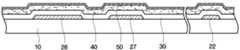
이하, 도 1a 및 도 1b를 참조하여, 본 발명의 제1 및 제2 실시예에 따른 박막 트랜지스터 표시판에 대하여 상세히 설명한다. 도 1a는 본 발명의 제1 및 제2 실시예에 따른 박막 트랜지스터 표시판의 배치도이다. 도 1b는 도 1a의 A-A'선을 따라 자른 본 발명의 제1 및 제2 실시예에 따른 박막 트랜지스터 표시판의 단면도이다.Hereinafter, the thin film transistor panel according to the first and second embodiments of the present invention will be described in detail with reference to FIGS. 1A and 1B. FIG. 1A is a layout diagram of a thin film transistor panel according to first and second embodiments of the present invention. 1B is a cross-sectional view of a thin film transistor panel according to the first and second embodiments of the present invention, taken along the line A-A 'in FIG. 1A.
도 1a 및 도 1b를 참조하면, 박막 트랜지스터 표시판은 소다석회유리(soda lime glass) 또는 보로 실리케이트 유리 등의 유리 또는 플라스틱 등으로 이루어진 절연 기판(10) 상에 형성된 박막 트랜지스터 등 다양한 소자들을 포함한다.1A and 1B, the thin film transistor display panel includes various elements such as a thin film transistor formed on an
절연 기판(10) 위에는 게이트 신호를 전달하는 게이트 배선(22, 26)이 형성되어 있다. 게이트 배선(22, 26)은 일 방향, 예를 들어 가로 방향으로 뻗어 있는 게이트선(22)과, 게이트선(22)으로부터 돌출되어 돌기 형태로 형성된 박막 트랜지스터의 게이트 전극(26)을 포함한다.On the
그리고 절연 기판(10) 위에는 공통 전압(common voltage)을 전달하고 스토리지 전극(27) 및 스토리지선(28)을 포함하는 스토리지 배선(27, 28)이 형성되어 있다. 스토리지선(28)은 게이트선(22)과 실질적으로 평행하게 가로 방향으로 형성될 수 있다. 스토리지 전극(27)은 스토리지선(28)보다 폭이 넓게 형성될 수 있다. 스토리지 전극(27)은 후술할 화소 전극(82)과 연결된 드레인 전극 확장부(67)와 중첩되어 화소의 전하 보존 능력을 향상시키는 스토리지 커패시터를 이룬다.
이와 같은 스토리지 배선(27, 28)의 모양 및 배치 등은 다양한 형태로 변형될 수 있으며, 화소 전극(82)과 게이트선(22)의 중첩으로 발생하는 스토리지 커패 시턴스가 충분할 경우 스토리지 배선(27, 28)이 형성되지 않을 수도 있다.The shape and arrangement of the
게이트 배선(22, 26) 및 스토리지 배선(27, 28)은 알루미늄(Al)과 알루미늄 합금 등 알루미늄 계열의 금속, 은(Ag)과 은 합금 등 은 계열의 금속, 구리(Cu)와 구리 합금 등 구리 계열의 금속, 몰리브덴(Mo)과 몰리브덴 합금 등 몰리브덴 계열의 금속, 크롬(Cr), 티타늄(Ti), 탄탈륨(Ta) 등으로 이루어질 수 있다. 또한, 게이트 배선(22, 26), 스토리지 전극(27) 및 스토리지선(28)은 물리적 성질이 다른 두 개의 도전막(미도시)을 포함하는 다중막 구조를 가질 수 있다. 이 중 한 도전막은 게이트 배선(22, 26) 및 스토리지 전극(27) 및 스토리지선(28)의 신호 지연이나 전압 강하를 줄일 수 있도록 낮은 비저항(resistivity)의 금속, 예를 들면 알루미늄 계열 금속, 은 계열 금속, 구리 계열 금속 등으로 이루어진다. 이와는 달리, 다른 도전막은 다른 물질, 특히 산화 아연(ZnO), ITO(indium tin oxide) 및 IZO(indium zinc oxide)와의 접촉 특성이 우수한 물질, 이를테면 몰리브덴 계열 금속, 크롬, 티타늄, 탄탈륨 등으로 이루어진다. 이러한 조합의 좋은 예로는 크롬 하부막과 알루미늄 상부막 및 알루미늄 하부막과 몰리브덴 상부막을 들 수 있다. 다만, 본 발명은 이에 한정되지 않으며, 게이트 배선(22, 26), 스토리지 배선(27, 28)은 다양한 여러 가지 금속과 도전체로 만들어질 수 있다.The
절연 기판(10), 게이트 배선(22, 26), 스토리지 배선(27, 28)의 위에는 예를 들어 산화 규소(SiOx) 또는 질화 규소(SiNx) 등으로 이루어진 게이트 절연막(30)이 형성되어 있다.A
게이트 절연막(30) 위에는 Zn, In, Ga, Sn 및 이들의 조합에서 선택된 물질 의 산화물로 이루어진 산화물 액티브층 패턴(42, 44)이 형성되어 있다. 산화물 액티브층 패턴(42, 44)에서 '액티브'란 구동 전류 인가시 전기적 특성을 가지게 되는 활성 물질을 의미하며, 반도체 및 금속 산화물 등을 모두 포함한다. 본 발명의 실시예들에 따른 산화물 액티브층 패턴(42, 44)은 적어도 하나의 제1 물질을 포함하며, 제1 물질의 산화물을 포함할 수 있다. 제1 물질은 아연 또는 인듐을 포함할 수 있다. 구체적으로 본 발명의 실시예들에 따른 산화물 액티브층 패턴(42, 44)은 예를 들어 InZnO, InGaO, InSnO, ZnSnO, GaSnO, GaZnO, GaZnSnO, GaInZnO, HfInZnO, 및 ZnO로 이루어진 군으로부터 선택된 어느 하나의 물질로 이루어질 수 있다.On the
본 발명의 실시예들에 따른 산화물 액티브층 패턴(42, 44)의 제1 물질의 산화물은 제1 깁스 자유 에너지(Gibbs free energy)를 가진다. 제1 깁스 자유 에너지는 후술하는 버퍼층 패턴(52, 55, 56, 57)에 포함된 제2 물질의 산화물이 가지는 제2 깁스 자유 에너지보다 작을 수 있다. 이에 대하여 이후에 상세히 설명한다.The oxide of the first material of the oxide
이러한 산화물 액티브층 패턴(42, 44)은 수소화 비정질 규소에 비하여 전하의 유효 이동도(effective mobility)가 2 내지 100배 정도 크고, 온/오프 전류비가 105 내지 108 의 값을 가짐으로써 뛰어난 반도체 특성을 가지고 있다. 또한 산화물 액티브층 패턴(42, 44)의 경우, 밴드갭(band gap)이 약 3.0 내지 3.5eV 이므로 가시광에 대하여 누설 광전류가 발생하지 않는다. 따라서 산화물 박막 트랜지스터의 순간 잔상을 방지할 수 있고, 산화물 박막 트랜지스터 하부에 광차단막을 형성할 필요가 없으므로 박막 트랜지스터 표시판의 개구율을 높일 수 있다. 산화물 반도체 의 특성을 향상시키기 위해 주기율표상의 3족, 4족, 5족 또는 전이원소가 추가로 포함될 수 있다. 또한, 산화물 액티브층 패턴(42, 44)은 비정질 상태이지만 높은 전하의 유효 이동도를 가지고 있고, 기존 비정질 규소의 제조 공정을 그대로 적용할 수 있어서 대면적 표시 장치에 대하여 적용할 수 있다.The oxide
산화물 액티브층 패턴(42, 44)과 데이터 배선(62, 65, 66, 67)의 패턴 형상은 서로 상이하거나 동일할 수 있다. 즉, 산화물 액티브층 패턴(42, 44) 게이트 전극(26)과 소스 전극(65) 및 드레인 전극(66)이 오버랩되는 부위에만 형성되어 섬형(island type) 형상을 가질 수 있다. 또한, 산화물 반도체 패턴(42, 44)은 산화물 박막 트랜지스터의 채널 영역을 제외하고는 후술할 데이터 배선(62, 65, 66, 67)과 실질적으로 동일한 형상을 가지는 선형(linear type) 형상을 가질 수도 있다.Pattern shapes of the oxide
산화물 액티브층 패턴(42, 44)의 상부에는 산화물 액티브층 패턴(42, 44)과 직접 접촉하도록 배치되고 제2 물질을 포함하는 버퍼층 패턴(52, 55, 56, 57)이 형성되어 있다. 버퍼층 패턴(52, 55, 56, 57)은 데이터 배선(62, 65, 66, 67)과 산화물 액티브층 패턴(42, 44)의 접촉 저항을 감소시키는 오믹 콘택층(ohmic contact layer)으로서 기능한다. 또한, 버퍼층 패턴(52, 55, 56, 57)은 산화물 액티브층 패턴(42, 44)에 포함되는 제1 물질이 환원되어 데이터 배선(62, 65, 66, 67)으로 석출되는 것을 방지하는 역할을 한다. 한편, 버퍼층 패턴(52, 55, 56, 57)에 포함되는 제2 물질은 제1 물질이 환원되어 버퍼층 패턴(52, 55, 56, 57)으로 석출되는 것을 방지할 수 있는 물질로부터 선택된다.On the oxide
이에 대하여 상세히 설명하면, 상술한 바와 같이 산화물 액티브층 패턴(42, 44)에 포함되는 제1 물질의 산화물이 가지는 제1 깁스 자유 에너지는 버퍼층 패턴(52, 55, 56, 57)에 포함된 제2 물질의 산화물이 가지는 제2 깁스 자유 에너지보다 작도록 선택한다. 다시 말해, 제1 물질과 산소의 결합력은 제2 물질과 산소의 결합력보다 작도록 산화물 액티브층 패턴(42, 44)에 포함되는 제1 물질과 버퍼층 패턴(52, 55, 56, 57)의 제2 물질이 선택된다.As described above, the first Gibbs free energy of the oxide of the first material contained in the oxide
구체적으로 제2 물질은 TiNx(x는 자연수), Mo, a-ITO, 및 IZO로 이루어진 군으로부터 선택된 어느 하나일 수 있다. 이들 제2 물질의 산화물의 제2 깁스 자유 에너지는 산화물 액티브층 패턴(42, 44)에 포함되는 제1 물질의 산화물이 가지는 제1 깁스 자유 에너지보다 크다. 예를 들어, 제1 물질의 산화물이 HfInZnO이고, 제2 물질이 TiNx인 경우 Hf의 산화물(HfO2), In의 산화물(InO2), 및 Zn의 산화물(ZnO)의 제1 깁스 자유 에너지는 모두 TiNx의 산화물의 제2 깁스 자유에너지보다 작다. 이에 따라, Hf, In, Zn 등의 제1 물질 중 어느 것도 버퍼층 패턴(52, 55, 56, 57)과 반응하여 버퍼층 패턴(52, 55, 56, 57)이나 데이터 배선(62, 65, 66, 67)측으로 석출되지 않고, 안정한 상태를 유지한다. 이에 반해, 후술하는 제1 비교예의 Ti 등을 제2 물질로 사용하여 버퍼층 패턴(52, 55, 56, 57)을 형성한 경우 In, Zn 등의 제1 물질이 버퍼층 패턴(52, 55, 56, 57)으로 석출되어 데이터 배선(62, 65, 66, 67)이 볼록하게 돌출되는 등의 외관 불량이 발생한다.Specifically, the second material may be any one selected from the group consisting of TiNx (x is a natural number), Mo, a-ITO, and IZO. The second Gibbs free energy of the oxides of these second materials is greater than the first Gibbs free energy of the oxides of the first material contained in the oxide
제1 및 제2 깁스 자유 에너지는 온도에 따라 달라질 수 있으며, 공정 온도 증가에 따라 깁스 자유 에너지가 급격하게 커지는 물질, 예를 들어 In 등의 경우를 고려하여 산화물 액티브층 패턴(42, 44), 버퍼층 패턴(52, 55, 56, 57), 및 데이터 배선(62, 65, 66, 67)은 낮은 온도에서 패턴을 형성할 수 있는 물질로부터 선택한다.The first and second Gibbs free energies may be varied depending on the temperature and the oxide
버퍼층 패턴(52, 55, 56, 57)의 두께는 50 ~ 1000Å, 바람직하게는 50 ~ 300Å인 것이 바람직하다. 버퍼층 패턴(52, 55, 56, 57)을 50Å 미만의 두께로 형성하는 경우 공정 수행이 어려울 수 있으며, 1000Å을 초과하는 두께로 형성하는 경우 저항 특성이 열화될 수 있다.The thickness of the
버퍼층 패턴(52, 55, 56, 57) 위에는 데이터 배선(62, 65, 66, 67)이 형성되어 있다. 데이터 배선(62, 65, 66, 67)은 예를 들어 세로 방향으로 형성되어 게이트선(22)과 교차하여 화소를 정의하는 데이터선(62)과, 데이터선(62)으로부터 분지되어 산화물 액티브층 패턴(42, 44)의 상부까지 연장되어 있는 소스 전극(65)과, 소스 전극(65)과 분리되어 있으며 게이트 전극(26) 또는 산화물 박막 트랜지스터의 채널부를 중심으로 소스 전극(65)과 대향하도록 산화물 액티브층 패턴(42, 44) 상부에 형성되어 있는 드레인 전극(66)과, 드레인 전극(66)으로부터 연장되어 스토리지 전극(27)과 중첩하는 넓은 면적의 드레인 전극 확장부(67)를 포함한다.On the
이러한 데이터 배선(62, 65, 66, 67)은 도 1b에 도시한 바와 같이 버퍼층 패턴(52, 55, 56, 57)과 직접 접촉하여 오믹 컨택(Ohmic contact)을 형성할 수 있다. 버퍼층 패턴(52, 55, 56, 57)이 오믹 컨택의 역할을 수행하므로 데이터 배선(62, 65, 66, 67)은 저저항 물질로 이루어진 단일층일 수 있다. 예를 들어 데이터 배 선(62, 65, 66, 67)은 Cu, Al, 또는 Ag로 이루어질 수 있다.The data lines 62, 65, 66 and 67 may be in direct contact with the
다만, 오믹 컨택 특성을 향상시키기 위해 데이터 배선(62, 65, 66, 67)은 Ni, Co, Ti, Ag, Cu, Mo, Al, Be, Nb, Au, Fe, Se, 또는 Ta 등으로 이루어진 단일막 또는 다중막 구조를 가질 수 있다. 다중막 구조의 예로는 Ta/Al, Ta/Al, Ni/Al, Co/Al, Mo(Mo 합금)/Cu, Mo(Mo 합금)/Cu, Ti(Ti 합금)/Cu, TiN(TiN 합금)/Cu, Ta(Ta 합금)/Cu, TiOx/Cu 등과 같은 이중막 또는 Ti/Al/Ti, Ta/Al/Ta, Ti/Al/TiN, Ta/Al/TaN, Ni/Al/Ni, Co/Al/Co 등과 같은 삼중막을 들 수 있다.The data lines 62, 65, 66, and 67 are formed of Ni, Co, Ti, Ag, Cu, Mo, Al, Be, Nb, Au, Fe, Se, Ta, or the like in order to improve the ohmic contact characteristics. May have a single-layer or multi-layer structure. Examples of the multilayer structure include Ta / Al, Ta / Al, Ni / Al, Co / Al, Mo (Mo alloy) / Cu, Mo (Mo alloy) / Cu, Ti (Ti alloy) / Cu, TiN Ti / Al / Ti, Ta / Al / TiN, Ta / Al / TaN, Ni / Al / Ni, Co / Al / Co, and the like.
소스 전극(65)은 산화물 액티브층 패턴(42, 44)과 적어도 일부분이 중첩되고, 드레인 전극(66)은 산화물 박막 트랜지스터의 채널부를 중심으로 소스 전극(65)과 대향하며 산화물 액티브층 패턴(42, 44)과 적어도 일부분이 중첩된다.The source electrode 65 overlaps at least a part of the oxide
데이터 배선(62, 65, 66, 67) 및 산화물 액티브층 패턴(42, 44) 상에는 보호막(70)이 형성되어 있다. 보호막(70)은 무기막 또는 유기막으로 형성될 수 있으며 산화물 반도체 패턴(44)을 보호하기 위하여 하부 무기막과 상부 유기막의 이중막 구조를 가질 수도 있다.A
박막 트랜지스터 표시판의 개구율을 향상시키기 위해 게이트 배선(22, 26) 및 데이터 배선(62, 65, 66, 67)은 모두 ITO(Indium Tin Oxide), IZO(Indium Zinc Oxide), 또는 AZO(Al doped zinc oxide) 등의 투명 전도성 물질로 이루어질 수도 있다.The gate wirings 22 and 26 and the data wirings 62 and 65 and 66 and 67 are formed of ITO (indium tin oxide), IZO (indium zinc oxide), or AZO (Al doped zinc) to improve the aperture ratio of the thin film transistor panel oxide) or the like.
보호막(70)에는 드레인 전극 확장부(67)를 드러내는 컨택홀(77)이 형성되어 있다. 보호막(70) 위에는 컨택홀(77)을 통하여 드레인 전극(66)과 전기적으로 연결 되는 화소 전극(82)이 형성되어 있다.The
화소 전극(82)은 ITO 또는 IZO 등의 투명 도전체 또는 알루미늄 등의 반사성 도전체로 이루어질 수 있다. 화소 전극(82)은 콘택홀(77)을 통하여 드레인 전극 확장부(67)와 전기적으로 연결되어 있다. 데이터 전압이 인가된 화소 전극(82)은 공통 전극 표시판(미도시)의 공통 전극(250)과 함께 전계를 생성함으로써 박막 트랜지스터 표시판과 공통 전극 표시판 사이에 개재된 액정층(미도시)의 액정 분자들을 회전시킨다.The
이하, 도 2a 내지 도 8c를 참조하여, 본 발명의 제1 및 제2 실시예에 따른 박막 트랜지스터 표시판과 비교예들의 박막 트랜지스터 표시판을 비교하여 설명한다. 도 2a 및 도 2b는 본 발명의 제1 실시예에 따른 박막 트랜지스터 표시판과 제1 비교예에 따른 박막 트랜지스터 표시판의 데이터 배선의 외관을 비교하여 나타낸 사진이다. 도 3은 제1 비교예에 따른 박막 트랜지스터 표시판의 데이터 배선의 외관을 확대하여 나타낸 사진이다. 도 4는 제1 비교예에 따른 박막 트랜지스터 표시판의 데이터 배선의 성분을 분석한 그래프이다. 도 5a 및 도 5b는 본 발명의 제1 실시예에 따른 박막 트랜지스터 표시판과 제1 비교예에 따른 박막 트랜지스터 표시판의 전압-전류 특성을 나타낸 그래프이다. 도 6a 내지 도 6c는 본 발명의 제2 실시예에 따른 박막 트랜지스터 표시판에 포함되는 산화물 반도체 패턴과 버퍼층 패턴의 반응 여부를 나타낸 그래프이다. 도 7a 내지 도 7c는 본 발명의 제1 비교예에 따른 박막 트랜지스터 표시판에 포함되는 산화물 반도체 패턴과 버퍼층 패턴의 반응 여부를 나타낸 그래프이다. 도 8a 내지 도 8c는 본 발명의 제2 비교예에 따른 박막 트랜지스터 표시판에 포함되는 산화물 반도체 패턴과 데이터 배선의 반응 여부를 나타낸 그래프이다.Hereinafter, the thin film transistor panel according to the first and second embodiments of the present invention and the thin film transistor panel according to the comparative example will be described with reference to FIGS. 2A to 8C. FIGS. 2A and 2B are photographs showing the appearance of data lines of the thin film transistor panel according to the first embodiment of the present invention and the thin film transistor panel according to the first comparative example. 3 is an enlarged photograph of the appearance of the data line of the thin film transistor panel according to the first comparative example. 4 is a graph showing the analysis of the data line components of the thin film transistor panel according to the first comparative example. 5A and 5B are graphs showing voltage-current characteristics of the thin film transistor panel according to the first embodiment of the present invention and the thin film transistor panel according to the first comparative example. FIGS. 6A to 6C are graphs showing the reaction between the oxide semiconductor pattern and the buffer layer pattern included in the thin film transistor panel according to the second embodiment of the present invention. 7A to 7C are graphs showing the reaction between the oxide semiconductor pattern and the buffer layer pattern included in the thin film transistor panel according to the first comparative example of the present invention. 8A to 8C are graphs showing the reaction between the oxide semiconductor pattern and the data line included in the thin film transistor panel according to the second comparative example of the present invention.
도 2a를 참조하면, 본 발명의 제1 실시예의 박막 트랜지스터 표시판의 데이터 배선(62, 65, 66, 67)의 표면은 패턴에 돌출부가 생성되거나 패턴이 박리되는 등의 불량이 거의 발생하지 않는다. 본 발명의 제1 실시예의 박막 트랜지스터 표시판은, 예를 들어 산화물 액티브층 패턴(42, 44)으로 HfInZnO를, 버퍼층 패턴(52, 55, 56, 57)으로 TiNx를, 데이터 배선(62, 65, 66, 67)으로 Cu 또는 Al을 사용한 것으로, Hf의 산화물(HfO2), In의 산화물(InO2), 및 Zn의 산화물(ZnO) 등의 제1 물질의 산화물의 제1 깁스 자유 에너지가 모두 TiNx의 산화물 즉, 제2 물질의 산화물의 제2 깁스 자유에너지보다 작아 산화물 액티브층 패턴(42, 44)이 안정하므로 산화물 액티브층 패턴(42, 44)을 구성하는 제1 물질들이 버퍼층 패턴(52, 55, 56, 57)이나 데이터 배선(62, 65, 66, 67)측으로 석출되지 않아 불량이 나타나지 않는다.2A, the surface of the data lines 62, 65, 66, and 67 of the thin film transistor panel according to the first embodiment of the present invention hardly causes defects such as protrusions on the patterns or peeling off of the patterns. The thin film transistor panel according to the first embodiment of the present invention is a thin film transistor panel in which HfInZnO is used as the oxide
도 2b를 참조하면, 본 발명의 제1 비교예에 따른 박막 트랜지스터 표시판의 데이터 배선(62, 65, 66, 67)의 표면은 패턴에 돌출부가 생성되거나 패턴이 박리되는 등의 불량이 발생한 검은색 점들을 확인할 수 있다. 본 발명의 제1 비교예에 따른 박막 트랜지스터 표시판은 산화물 액티브층 패턴(42, 44)으로 HfInZnO를, 버퍼층 패턴(52, 55, 56, 57)으로 Ti를, 데이터 배선(62, 65, 66, 67)으로 Cu를 사용한 것이다. 이 경우 Hf의 산화물(HfO2), In의 산화물(InO2), 및 Zn의 산화물(ZnO)의 제 1 깁스 자유 에너지 중 적어도 하나는 Ti의 산화물의 제2 깁스 자유에너지보다 크다. 따라서, Hf, In, Zn 등의 제1 물질 중 적어도 하나의 산화물은 버퍼층 패턴(52, 55, 56, 57)을 구성하는 제2 물질 즉, Ti와 반응하여 버퍼층 패턴(52, 55, 56, 57)이나 데이터 배선(62, 65, 66, 67)측으로 석출되며, 이는 외관 불량으로 나타난다.2B, the surfaces of the data lines 62, 65, 66, and 67 of the thin film transistor panel according to the first comparative example of the present invention are formed in black (black) in which defects such as protrusions are formed in the patterns, You can see the points. In the thin film transistor panel according to the first comparative example of the present invention, HfInZnO as the oxide
도 3을 참조하면, 제1 비교예의 박막 트랜지스터 표시판의 데이터 배선에 산화물 액티브층 패턴을 구성하는 물질이 석출되어 돌출된 모습을 확인할 수 있다. 이는 데이터 배선과 화소 전극의 접촉 특성을 약화시키고 저항을 증가시킬 수 있으며, 누설 전류를 발생시킬 수 있다.Referring to FIG. 3, it can be seen that the material of the oxide active layer pattern is deposited and protruded on the data line of the thin film transistor panel of the first comparative example. This can weaken the contact characteristics between the data line and the pixel electrode, increase the resistance, and generate a leakage current.
도 4를 참조하면, 제1 비교예의 박막 트랜지스터 표시판의 데이터 배선에는 산화물 액티브층 패턴의 제1 물질들이 석출된 것을 확인할 수 있다. 도 4는 제1 비교예의 박막 트랜지스터 표시판의 데이터 배선을 EDX(Energy Dispersive X-ray spectroscopy)로 측정한 것으로 X 선의 에너지 총량에 대하여 석출된 제1 물질들의 량을 나타낸 것이다. 도 4에서 x축은 X 선의 에너지 총량(eV)을 y축은 석출된 각 성분의 원자 단위의 세기(a.u : atomic unit)를 의미한다.Referring to FIG. 4, it can be seen that the first materials of the oxide active layer pattern are deposited on the data lines of the thin film transistor panel of the first comparative example. FIG. 4 is a graph showing the amount of the first substances precipitated with respect to the total amount of energy of X-rays measured by EDX (Energy Dispersive X-ray spectroscopy) of the data line of the thin film transistor panel of the first comparative example. In FIG. 4, the x-axis represents the total energy amount (eV) of the X-ray, and the y-axis represents the atomic unit (au) of each component of the precipitated component.
도 4에서 측정된 각 원소의 석출량을 정량적으로 나타내면 하기 표 1과 같다.The amount of precipitation of each element measured in FIG. 4 is quantitatively shown in Table 1 below.
(표 1)(Table 1)
상기 표 1을 참조하면, 제1 비교예의 산화물 액티브층 패턴을 구성하는 제1 물질 중, 특히 In이 많이 석출된 것을 확인할 수 있다. 이는 In 산화물의 제1 깁스 에너지가 Ti 산화물의 제2 깁스 에너지보다 커서 In이 버퍼층 패턴을 구성하는 제2 물질과 반응하고, 환원된 In이 버퍼층 패턴 및 데이터 배선으로 석출되었기 때문이다.Referring to Table 1, it can be seen that a large amount of In was precipitated out of the first materials constituting the oxide active layer pattern of the first comparative example. This is because the first Gibbs energy of the In oxide is larger than the second Gibbs energy of the Ti oxide so that In reacts with the second material constituting the buffer layer pattern and the reduced In is precipitated in the buffer layer pattern and the data wiring.
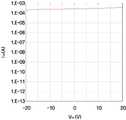
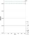
도 5a를 참조하면, 본 발명의 제1 실시예에 따른 박막 트랜지스터 표시판은 게이트 전압(VGS)가 증가함에 따라 소스-드레인 전류(Ids)가 증가하여 박막 트랜지스터의 특징을 가짐을 확인할 수 있다. 그러나, 도 5b를 참조하면, 제1 비교예의 박막 트랜지스터 표시판은 게이트 전압(VGS)가 증가하더라도 소스-드레인 전류(Ids)가 일정하여 박막 트랜지스터의 특징을 나타내지 않음을 확인할 수 있다. 따라서, 제1 비교예와 같이 산화물 액티브층 패턴(42, 44)으로 HfInZnO를, 버퍼층 패턴(52, 55, 56, 57)으로 Ti를 사용하면 박막 트랜지스터 표시판으로 사용될 수 없다.Referring to FIG. 5A, the thin film transistor display panel according to the first embodiment of the present invention increases the source-drain current Ids as the gate voltage VGS increases, and thus has characteristics of the thin film transistor. However, referring to FIG. 5B, it can be seen that the source-drain current Ids is constant even when the gate voltage VGS increases, and the characteristics of the thin film transistor are not shown in the thin film transistor panel of the first comparative example. HfInZnO as the oxide
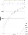
도 6a 내지 도 6c를 참조하면, 본 발명의 제2 실시예에 따른 박막 트랜지스터 표시판의 산화물 액티브층 패턴(42, 44)을 구성하는 제1 물질의 산화물은 버퍼층 패턴(52, 55, 56, 57)을 구성하는 제2 물질과 반응하지 않을 확인할 수 있다.6A to 6C, oxides of the first material constituting the oxide
본 발명의 제2 실시예에 따른 박막 트랜지스터 표시판은, 예를 들어 산화물 액티브층 패턴(42, 44)으로 GaInZnO, HfInZnO, 또는 ZnO를, 버퍼층 패턴(52, 55, 56, 57)으로 Mo를, 데이터 배선(62, 65, 66, 67)으로 Cu 또는 Al을 사용한 것이다. 도 6a, 도 6b, 및 도 6c는 각각 산화물 액티브층 패턴(42, 44)의 제1 물질의 산화물로 GaInZnO, HfInZnO, 및 ZnO를 사용하고, 제2 물질로 충분량의 Mo을 사용하여 제1 물질의 산화물과 제2 물질의 반응 여부를 확인한 것이다. 도 6a 내지 도 8c에서 Ga:In:Zn의 몰비는 2:2:1로, Hf:In:Zn의 몰비는 0.23:2:2로 설정하였다. 도 6a 내지 도 6c에서 확인할 수 있는 바와 같이 고온 영역에서 Mo 산화물의 증가가 확인되지만 저온 영역에서는 관찰되지 않으며, Hf, Ga, In 등 제1 물질의 석출량은 미미하거나 없는 것을 확인할 수 있다. Zn의 경우 저온 영역에서의 석출량은 미미한 것을 확인할 수 있다. 따라서, 상술한 제1 물질 및 제2 물질을 포함하는 본 발명의 제2 실시예의 박막 트랜지스터 표시판은 산화물 액티브층 패턴(42, 44)에 포함된 제1 물질이 버퍼층 패턴(52, 55, 56, 57) 또는 데이터 배선(62, 65, 66, 67)으로 석출되지 않고 균일한 데이터 배선(62, 65, 66, 67) 표면을 제공한다.The thin film transistor panel according to the second embodiment of the present invention can be formed by using GaInZnO, HfInZnO or ZnO as the oxide
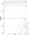
본 발명의 제1 비교예에 따른 박막 트랜지스터 표시판은, 예를 들어 산화물 액티브층 패턴으로 GaInZnO, HfInZnO, 또는 ZnO를, 버퍼층 패턴으로 Ti를, 데이터 배선으로 Cu 또는 Al을 사용한 것이다. 도 7a, 도 7b, 및 도 7c는 각각 산화물 액티브층 패턴의 제1 물질의 산화물로 GaInZnO, HfInZnO, 및 ZnO를 사용하고, 제2 물질로 충분량의 Ti를 사용하여 제1 물질의 산화물과 제2 물질의 반응 여부를 확인한 것이다. 도 7a 내지 도 7c에서 확인할 수 있는 바와 같이 저온 영역 및 고온 영역 에서 Ti 산화물의 증가가 확인된다. 또한 Hf를 제외하고 Ga, In 등 제1 물질이 다량 석출됨을 확인할 수 있다. 따라서, 상술한 제1 물질 및 제2 물질을 포함하는 본 발명의 제1 비교예의 박막 트랜지스터 표시판은 산화물 액티브층 패턴에 포함된 제1 물질이 버퍼층 패턴 또는 데이터 배선으로 석출되어 불량을 일으키고 박막 트랜지스터 표시판으로 사용할 수 없다.The thin film transistor panel according to the first comparative example of the present invention uses, for example, GaInZnO, HfInZnO, or ZnO as the oxide active layer pattern, Ti as the buffer layer pattern, and Cu or Al as the data wiring. Figs. 7a, 7b and 7c are graphs respectively showing the results of using GaInZnO, HfInZnO, and ZnO as oxides of the first material of the oxide active layer pattern, and using oxides of the first material and Ti It confirms whether the substance is reacting. As can be seen from Figs. 7A to 7C, an increase in Ti oxide is confirmed in the low-temperature region and the high-temperature region. In addition, it can be confirmed that a large amount of the first substance such as Ga and In is precipitated except Hf. Accordingly, in the thin film transistor panel according to the first comparative example of the present invention including the first material and the second material, the first material included in the oxide active layer pattern is deposited on the buffer layer pattern or the data line to cause defects, Can not be used.
본 발명의 제2 비교예에 따른 박막 트랜지스터 표시판은, 예를 들어 산화물 액티브층 패턴으로 GaInZnO, HfInZnO, 또는 ZnO를 사용하고, 버퍼층 패턴(52, 55, 56, 57)을 사용하지 않으며, 데이터 배선으로 Al을 사용한 것이다. 도 8a, 도 8b, 및 도 8c는 각각 산화물 액티브층 패턴의 제1 물질의 산화물로 GaInZnO, HfInZnO, 및 ZnO를 사용하고, 충분량의 Ti를 사용하여 제1 물질의 산화물과 Ti의 반응 여부를 확인한 것이다. 도 8a 내지 도 8c에서 확인할 수 있는 바와 같이 저온 영역 및 고온 영역에서 Al 산화물의 증가가 확인된다. 또한 Hf, Ga, In 등 제1 물질이 다량 석출됨을 확인할 수 있다. 따라서, 상술한 제1 물질 및 Al 을 포함하는 본 발명의 제1 비교예의 박막 트랜지스터 표시판은 산화물 액티브층 패턴(42, 44)에 포함된 제1 물질이 데이터 배선으로 석출되어 불량을 일으키고 박막 트랜지스터 표시판으로 사용할 수 없다.The thin film transistor panel according to the second comparative example of the present invention is a thin film transistor panel in which GaInZnO, HfInZnO, or ZnO is used as an oxide active layer pattern and the
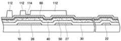
이하, 도 1b 및 도 9 내지 도 19를 참조하여, 본 발명의 제3 실시예에 따른 박막 트랜지스터 표시판에 대하여 상세히 설명한다. 도 9 내지 도 18은 본 발명의 제3 실시예에 따른 박막 트랜지스터 표시판의 제조 방법을 공정 단계별로 나타낸 단면도이다. 도 19는 본 발명의 제3 실시예에 따른 박막 트랜지스터 표시판의 제조 방법 중 공정 조건을 나타낸 그래프이다.Hereinafter, a thin film transistor panel according to a third embodiment of the present invention will be described in detail with reference to FIG. 1B and FIGS. 9 to 19. FIG. 9 to 18 are cross-sectional views illustrating a method of manufacturing a thin film transistor panel according to a third embodiment of the present invention. 19 is a graph showing process conditions in a method of manufacturing a thin film transistor panel according to the third embodiment of the present invention.
먼저, 도 9에 도시된 바와 같이, 절연 기판(10) 위에 게이트 배선용 금속막(미도시)을 적층한 후, 이를 패터닝하여 게이트선(22), 게이트 전극(26), 스토리지 전극(27), 스토리지선(28)을 포함하는 게이트 배선(22, 26, 27, 28)을 형성한다.9, a metal film for gate wirings (not shown) is deposited on the insulating
여기서 게이트선(22), 게이트 전극(26), 스토리지 전극(27) 및 스토리지선(28)을 포함하는 게이트 배선(22, 26, 27, 28)을 형성하기 위해 스퍼터링(sputtering)법을 이용할 수 있다. 스퍼터링은 200℃ 이하의 저온 공정에서 수행하며, 이러한 저온의 스퍼터링 방식으로 게이트 배선(22, 26, 27, 28)을 형성함으로써 예를 들어 소다석회유리로 이루어진 절연 기판(10)의 열화를 방지할 수 있다. 이어서, 이들 도전막을 습식 식각 또는 건식 식각하여 패터닝한다. 습식 식각의 경우, 인산, 질산, 초산 등의 식각액을 사용할 수 있다.Here, a sputtering method can be used to form the gate wirings 22, 26, 27, and 28 including the
이어서, 절연 기판(10) 및 게이트 배선(22, 26, 27, 28)의 위에 질화 규소(SiNx) 등으로 이루어진 게이트 절연막(30)을 예를 들어, 플라즈마 강화 화학 기상 증착법(Plasma Enhanced CVD, PECVD) 또는 리액티브 스퍼터링(reactive sputtering)을 이용하여 증착한다. 절연 기판(10)이 열적 내성이 약한 물질로 이루어진 경우 게이트 절연막(30) 형성시에도 130℃ 이하의 저온 공정을 이용하는 것이 바람직함은 물론이다.A
이어서, 예를 들어, 스퍼터링 또는 화학 기상 증착법을 이용하여 게이트 절연막(30) 위에 산화물 액티브층(40)을 증착한다. 산화물 액티브층(40)에서 '액티브'란 구동 전류 인가시 전기적 특성을 가지게 되는 활성 물질을 의미하며, 반도체 및 금속 산화물 등을 모두 포함한다. 산화물 액티브층(40)은 제1 물질의 산화물 예를 들어 InZnO, InGaO, InSnO, ZnSnO, GaSnO, GaZnO, GaZnSnO, GaInZnO, HfInZnO, 및 ZnO로 이루어진 군으로부터 선택된 어느 하나의 물질로 이루어질 수 있다.Then, an oxide
이어서, 도 10 및 도 20을 참조하면, 예를 들어 스퍼터링 또는 화학 기상 증착법을 이용하여 산화물 액티브층(40) 위에 버퍼층(50)을 증착한다. 본 실시예의 버퍼층(50)은 제2 물질을 포함하며, 제2 물질은 예를 들어 TiNx, Mo, a-ITO, 및 IZO로 이루어진 군으로부터 선택된 어느 하나일 수 있다. 제1 물질의 산화물의 제1 깁스 자유 에너지는 제2 물질의 산화물의 제2 깁스 자유에너지보다 작다. 버퍼층(50)의 형성은 Ar 및 N2를 반응 가스로 이용하여 Ti를 스퍼터링함으로써 이루어질 수 있다. 이 경우 Ar 및 N2의 유량비는 Ar : N2의 유량비는 20 : 80 내지 5 : 95일 수 있다. 도 20에서 확인하 수 있는 바와 같이 이와 같이 증착하면 TiNx로 이루어진 버퍼층(50)을 형성할 수 있다.10 and 20, a
이어서, 도 11을 참조하면, 버퍼층(50) 상에 데이터 배선용 도전막(60)을 예를 들어, 스퍼터링을 이용하여 증착한다. 이어서 데이터 배선용 도전막(60)의 상부에 포토레지스트막(110)을 도포한다. 본 실시예의 데이터 배선용 도전막(60)은 본 발명의 제1 실시예에 따른 데이터 배선(미도시)의 구성 물질과 동일하며, Al 또는 Cu를 포함할 수 있다. 데이터 배선용 도전막(60)은 80 내지 100℃의 저온에서 증착한다. 이와 같이 저온에서 데이터 배선용 도전막(60)을 형성하는 경우 산화물 반도체층(40)과 버퍼층(50)의 반응이 방지되어 산화물 반도체층(40)에 포함된 제1 물질이 데이터 배선용 도전막(60)측으로 석출되지 않는다.Next, referring to FIG. 11, a
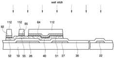
이어서, 도 12를 참조하면, 마스크를 통하여 포토레지스트막(110)에 빛을 조사한 후 현상하여, 포토레지스트막 패턴(112, 114)을 형성한다. 이때 포토레지스트막 패턴(112, 114) 중에서 박막 트랜지스터의 채널부, 즉 소스 전극(도 15의 65 참조)과 드레인 전극(도 15의 66 참조) 사이에 위치한 토레지스트막 패턴(114)은 데이터 배선부, 즉 데이터 배선이 형성될 부분에 위치한 포토레지스트막 패턴(112)보다 두께가 얇게 되도록 하며, 채널부와 데이터 배선부를 제외한 기타 부분의 포토레지스트막은 모두 제거한다. 이 때 채널부에 남아 있는 포토레지스트막 패턴(114)의 두께와 데이터 배선부에 남아 있는 포토레지스트막 패턴(112)의 두께의 비는 후술할 식각 공정에서의 공정 조건에 따라 다를 수 있다.12, the
이와 같이, 위치에 따라 포토레지스트막의 두께를 달리하는 방법으로 여러 가지가 있을 수 있으며, 빛 투과량을 조절하기 위하여 주로 슬릿(slit), 격자 형태의 패턴 또는 반투명막을 이용한 마스크를 사용할 수 있다. 또한 리플로우가 가능한 물질로 이루어진 포토레지스트막을 이용하여 빛이 완전히 투과할 수 있는 부분과 빛이 완전히 투과할 수 없는 부분으로 나뉘어진 통상적인 마스크로 노광한 다음 현상하고 리플로우시켜 포토레지스트막이 잔류하지 않는 부분으로 포토레지스트막의 일부를 흘러내리도록 함으로써 이러한 얇은 두께의 포토레지스트막 패턴(114)을 형성할 수도 있다.As described above, there may be various methods of varying the thickness of the photoresist film depending on the position, and a mask using a slit, a lattice pattern, or a semi-transparent film may be used to adjust the light transmittance. In addition, a photoresist film made of a reflowable material is used to expose the photoresist film with a conventional mask, which is divided into a portion through which light can be completely transmitted and a portion through which light can not be completely transmitted, and then developed and reflowed to leave a photoresist film The
이어서, 도 12 및 도 13을 참조하면 포토레지스트막 패턴(112, 114)을 식각마스크로 이용하여 데이터 배선용 도전막(60)을 식각한다. 이러한 식각은 습식 식각 또는 건식 식각을 이용할 수 있다. 습식 식각의 경우 인산, 질산 및 초산의 혼 합액, 불산(HF) 및 탈이온수(deionized water)의 혼합액 등의 식각액을 사용할 수 있다. 이렇게 하면, 데이터선(62) 및 소스/드레인용 도전막 패턴(64)만이 남고 이를 제외한 기타 부분의 데이터 배선용 도전막(60)은 모두 제거되어 그 하부의 산화물 액티브층(40)이 노출된다. 이 때 남은 데이터선(62) 및 소스/드레인용 도전막 패턴(64)은 소스 전극(도 15의 65 참조) 및 드레인 전극(도 15의 66 참조)이 분리되지 않고 연결되어 있는 점을 제외하면 데이터 배선(도 15의 62, 65, 66, 67 참조)의 형태와 동일하다.Next, referring to FIGS. 12 and 13, the data wiring
이어서, 도 13 및 도 14를 참조하면, 포토레지스트막 패턴(112, 114)을 에치백(etch-back)하여 채널부의 포토레지스트막 패턴(114)을 제거한다. 이어서 애싱(ashing)을 통하여 채널부의 소스/드레인용 도전막 패턴(64) 표면에 남아 있는 포토레지스트막 잔재를 제거한다. 이어서, 포토레지스트막 패턴(112)을 식각 마스크로 이용하여 채널부의 소스/드레인용 도전막 패턴(64)을 습식 식각 또는 건식 식각한다. 습식 식각의 경우 예를 들어 인산, 질산 및 초산의 혼합액, 불산(HF) 및 탈이온수(deionized water)의 혼합액 등의 식각액을 사용할 수 있다. 이렇게 하면, 소스 전극(65)과 드레인 전극(66)이 분리되면서 데이터 배선(62, 65, 66, 67)이 완성된다. 포토레지스트막 패턴(112)을 식각 마스크로 하여 버퍼층(50)에 대한 식각을 진행하여 버퍼층 패턴(52, 55, 56, 57)을 형성한다. 본 실시예의 버퍼층(50)의 식각은 건식 식각으로 진행될 수 있다. 이 경우 식각 가스로 버퍼층(50)에 대한 식각 선택비가 높아 산화물 액티브층(40)은 식각되지 않는 것을 사용한다. 이러한 예로 SF6와 O2의 혼합가스 또는 Cl2와 O2의 혼합 가스가 적합하게 예시된다. 이와 같 이 버퍼층(50)을 건식 식각하여 미완성 버퍼층 패턴(51, 52)을 형성함으로써 산화물 액티브층(40)에 대한 손상이 감소한다.Next, referring to FIGS. 13 and 14, the
이어서, 도 15를 참조하면, 산화물 액티브층(40)에 대한 식각을 진행하여 산화물 액티브층 패턴(42, 44)을 형성한다. 이 경우 산화물 액티브층(40)만 식각되고 게이트 절연막(30)은 식각되지 않는 것이 바람직하다. 이러한 식각은 습식 식각 또는 건식 식각을 이용할 수 있다. 습식 식각의 경우 불산(HF), 황산, 염산 및 이들의 조합에 탈이온수를 혼합한 식각액을 사용할 수 있다. 건식 식각의 경우, 불소 계열의 식각 가스, 예를 들어 CHF3, CF4 등을 사용할 수 있다. 구체적으로 불소 계열의 식각 가스에 Ar 또는 He이 함유된 식각 가스를 사용할 수 있다. 채널부의 산화물 액티브층 패턴(44)의 일부도 소정의 두께만큼 제거할 수도 있다.15, the etching for the oxide
이어서 도 15 및 도 16을 참조하면, 데이터 배선(62, 65, 66, 67) 상에 남아 있는 포토레지스트막 패턴(112)을 제거한다.15 and 16, the
이어서, 도 16 및 도 17을 참조하면, 산화물 액티브층 패턴(42, 44) 및 데이터 배선(62, 65, 66, 67) 상에 질화 규소로 이루어진 보호막을 형성한다. 보호막(70)은, 예를 들어 반응성 화학 기상 증착법을 이용하여 증착할 수 있다.16 and 17, a protective film made of silicon nitride is formed on the oxide
이어서, 도 18에 도시된 바와 같이, 보호막(70)을 사진 식각하여 드레인 전극 확장부(67)를 드러내는 콘택홀(77)을 형성한다.Then, as shown in FIG. 18, the
마지막으로, 예를 들어 ITO, IZO 등과 같은 투명 도전체 또는 반사성 도전체를 증착하고 사진 식각하여 드레인 전극 확장부(67)와 연결된 화소 전극(82)을 형 성하여 도 1b의 박막 트랜지스터 표시판을 완성한다.Finally, a transparent conductor such as ITO, IZO, or the like is deposited and photolithographically etched to form a
이어서, 도 1b 및 도 20을 참조하여, 본 발명의 제4 실시예에 따른 박막 트랜지스터 표시판에 대하여 설명한다. 도 20은 본 발명의 제4 실시예에 따른 박막 트랜지스터 표시판의 제조 방법을 나타낸 단면도이다.Next, a thin film transistor panel according to a fourth embodiment of the present invention will be described with reference to FIG. 1B and FIG. 20 is a cross-sectional view illustrating a method of manufacturing a thin film transistor panel according to a fourth embodiment of the present invention.
먼저, 도 9에 도시한 바와 같은 공정을 거쳐 산화물 액티브층(40)을 형성한다.First, an oxide
이어서, 도 10을 참조하면, 제2 물질로 Mo를 포함하는 버퍼층(50)을 산화물 액티브층(40)을 형성한다.Next, referring to FIG. 10, a
이어서, 도 11 내지 도 13에 도시한 공정을 수행한다.Then, the processes shown in Figs. 11 to 13 are performed.
이어서, 도 20을 참조하면, 습식 식각법을 이용하여 버퍼층(50)을 식각하여 버퍼층 패턴(52, 55, 56, 57)을 형성한다. 이 경우 산화물 액티브층(40)에 손상이 감소되도록 높은 선택비를 가진 물질을 식각 물질로 사용한다. 소스/드레인용 도전막 패턴(64)과 버퍼층(50)의 식각은 동일한 식각액을 이용하여 연속적으로 수행될 수도 있다.Next, referring to FIG. 20, the
이상 첨부된 도면을 참조하여 본 발명의 실시예들을 설명하였지만, 본 발명이 속하는 기술분야에서 통상의 지식을 가진 자는 본 발명이 그 기술적 사상이나 필수적인 특징을 변경하지 않고서 다른 구체적인 형태로 실시될 수 있다는 것을 이해할 수 있을 것이다. 그러므로 이상에서 기술한 실시예들은 모든 면에서 예시적인 것이며 한정적이 아닌 것으로 이해해야만 한다.While the present invention has been described in connection with what is presently considered to be practical exemplary embodiments, it is to be understood that the invention is not limited to the disclosed embodiments, but, on the contrary, You will understand. It is therefore to be understood that the above-described embodiments are illustrative in all aspects and not restrictive.
도 1a는 본 발명의 제1 및 제2 실시예에 따른 박막 트랜지스터 표시판의 배치도이다.1A is a layout diagram of a thin film transistor panel according to first and second embodiments of the present invention.
도 1b는 도 1a의 A-A'선을 따라 자른 본 발명의 제1 및 제2 실시예에 따른 박막 트랜지스터 표시판의 단면도이다.1B is a cross-sectional view of a thin film transistor panel according to the first and second embodiments of the present invention, taken along the line A-A 'in FIG. 1A.
도 2a 및 도 2b는 본 발명의 제1 실시예에 따른 박막 트랜지스터 표시판과 제1 비교예에 따른 박막 트랜지스터 표시판의 데이터 배선의 외관을 비교하여 나타낸 사진이다.FIGS. 2A and 2B are photographs showing the appearance of data lines of the thin film transistor panel according to the first embodiment of the present invention and the thin film transistor panel according to the first comparative example.
도 3은 제1 비교예에 따른 박막 트랜지스터 표시판의 데이터 배선의 외관을 확대하여 나타낸 사진이다.3 is an enlarged photograph of the appearance of the data line of the thin film transistor panel according to the first comparative example.
도 4는 제1 비교예에 따른 박막 트랜지스터 표시판의 데이터 배선의 성분을 분석한 그래프이다.4 is a graph showing the analysis of the data line components of the thin film transistor panel according to the first comparative example.
도 5a 및 도 5b는 본 발명의 제1 실시예에 따른 박막 트랜지스터 표시판과 제1 비교예에 따른 박막 트랜지스터 표시판의 전압-전류 특성을 나타낸 그래프이다.5A and 5B are graphs showing voltage-current characteristics of the thin film transistor panel according to the first embodiment of the present invention and the thin film transistor panel according to the first comparative example.
도 6a 내지 도 6c는 본 발명의 제2 실시예에 따른 박막 트랜지스터 표시판에 포함되는 산화물 반도체 패턴과 버퍼층 패턴의 반응 여부를 나타낸 그래프이다.FIGS. 6A to 6C are graphs showing the reaction between the oxide semiconductor pattern and the buffer layer pattern included in the thin film transistor panel according to the second embodiment of the present invention.
도 7a 내지 도 7c는 본 발명의 제1 비교예에 따른 박막 트랜지스터 표시판에 포함되는 산화물 반도체 패턴과 버퍼층 패턴의 반응 여부를 나타낸 그래프이다.7A to 7C are graphs showing the reaction between the oxide semiconductor pattern and the buffer layer pattern included in the thin film transistor panel according to the first comparative example of the present invention.
도 8a 내지 도 8c는 본 발명의 제2 비교예에 따른 박막 트랜지스터 표시판에 포함되는 산화물 반도체 패턴과 데이터 배선의 반응 여부를 나타낸 그래프이다.8A to 8C are graphs showing the reaction between the oxide semiconductor pattern and the data line included in the thin film transistor panel according to the second comparative example of the present invention.
도 9 내지 도 18은 본 발명의 제3 실시예에 따른 박막 트랜지스터 표시판의 제조 방법을 공정 단계별로 나타낸 단면도이다.9 to 18 are cross-sectional views illustrating a method of manufacturing a thin film transistor panel according to a third embodiment of the present invention.
도 19는 본 발명의 제3 실시예에 따른 박막 트랜지스터 표시판의 제조 방법 중 공정 조건을 나타낸 그래프이다.19 is a graph showing process conditions in a method of manufacturing a thin film transistor panel according to the third embodiment of the present invention.
도 20은 본 발명의 제4 실시예에 따른 박막 트랜지스터 표시판의 제조 방법을 나타낸 단면도이다.20 is a cross-sectional view illustrating a method of manufacturing a thin film transistor panel according to a fourth embodiment of the present invention.
(도면의 주요부분에 대한 부호의 설명) DESCRIPTION OF THE REFERENCE NUMERALS (S)
10: 절연 기판22: 게이트선10: insulating substrate 22: gate line
26: 게이트 전극27: 스토리지 전극26: gate electrode 27: storage electrode
28: 스토리지선30: 게이트 절연막28: Stagger line 30: Gate insulating film
40: 산화물 액티브층42, 44: 산화물 액티브층 패턴40: oxide
60: 데이터 배선용 도전막62: 데이터선60: conductive film for data wiring 62: data line
64: 소스/드레인용 도전막 패턴65: 소스 전극64: conductive film pattern for source / drains 65: source electrode
66: 드레인 전극67: 드레인 전극 확장부66: drain electrode 67: drain electrode extension part
70: 보호막77: 콘택홀70: Shielding film 77: Contact hole
82: 화소 전극110: 포토레지스트막82: pixel electrode 110: photoresist film
112, 114: 포토레지스트막 패턴112 and 114: photoresist film pattern
Claims (22)
Translated fromKoreanPriority Applications (2)
| Application Number | Priority Date | Filing Date | Title |
|---|---|---|---|
| KR1020080128678AKR101609727B1 (en) | 2008-12-17 | 2008-12-17 | Thin film transistor substrate and method of fabricating thereof |
| US12/498,816US8035110B2 (en) | 2008-12-17 | 2009-07-07 | Thin-film transistor substrate having oxide active layer patterns and method of fabricating the same |
Applications Claiming Priority (1)
| Application Number | Priority Date | Filing Date | Title |
|---|---|---|---|
| KR1020080128678AKR101609727B1 (en) | 2008-12-17 | 2008-12-17 | Thin film transistor substrate and method of fabricating thereof |
Publications (2)
| Publication Number | Publication Date |
|---|---|
| KR20100070081A KR20100070081A (en) | 2010-06-25 |
| KR101609727B1true KR101609727B1 (en) | 2016-04-07 |
Family
ID=42239429
Family Applications (1)
| Application Number | Title | Priority Date | Filing Date |
|---|---|---|---|
| KR1020080128678AActiveKR101609727B1 (en) | 2008-12-17 | 2008-12-17 | Thin film transistor substrate and method of fabricating thereof |
Country Status (2)
| Country | Link |
|---|---|
| US (1) | US8035110B2 (en) |
| KR (1) | KR101609727B1 (en) |
Families Citing this family (21)
| Publication number | Priority date | Publication date | Assignee | Title |
|---|---|---|---|---|
| US8247276B2 (en) | 2009-02-20 | 2012-08-21 | Semiconductor Energy Laboratory Co., Ltd. | Thin film transistor, method for manufacturing the same, and semiconductor device |
| KR101810699B1 (en) | 2009-06-30 | 2018-01-25 | 가부시키가이샤 한도오따이 에네루기 켄큐쇼 | Method for manufacturing semiconductor device |
| KR102011616B1 (en) | 2009-06-30 | 2019-08-16 | 가부시키가이샤 한도오따이 에네루기 켄큐쇼 | Method for manufacturing semiconductor device |
| KR101320229B1 (en)* | 2009-07-27 | 2013-10-21 | 가부시키가이샤 고베 세이코쇼 | Wiring structure and display apparatus having wiring structure |
| TWI467770B (en)* | 2009-10-26 | 2015-01-01 | Prime View Int Co Ltd | Display and its thin film transistor array substrate and thin film transistor |
| KR101370301B1 (en) | 2009-11-20 | 2014-03-05 | 가부시키가이샤 한도오따이 에네루기 켄큐쇼 | Method for manufacturing semiconductor device |
| WO2011065243A1 (en) | 2009-11-28 | 2011-06-03 | Semiconductor Energy Laboratory Co., Ltd. | Semiconductor device and manufacturing method thereof |
| KR101700882B1 (en)* | 2010-05-20 | 2017-02-01 | 삼성디스플레이 주식회사 | Oxide semiconductor thin film transistor |
| US9209314B2 (en)* | 2010-06-16 | 2015-12-08 | Semiconductor Energy Laboratory Co., Ltd. | Field effect transistor |
| WO2012002040A1 (en)* | 2010-07-01 | 2012-01-05 | Semiconductor Energy Laboratory Co., Ltd. | Driving method of liquid crystal display device |
| KR20250021395A (en)* | 2010-07-02 | 2025-02-12 | 가부시키가이샤 한도오따이 에네루기 켄큐쇼 | Semiconductor device and manufacturing method thereof |
| US8797303B2 (en) | 2011-03-21 | 2014-08-05 | Qualcomm Mems Technologies, Inc. | Amorphous oxide semiconductor thin film transistor fabrication method |
| US9379254B2 (en) | 2011-11-18 | 2016-06-28 | Qualcomm Mems Technologies, Inc. | Amorphous oxide semiconductor thin film transistor fabrication method |
| KR101987688B1 (en)* | 2011-12-13 | 2019-06-12 | 엘지디스플레이 주식회사 | Method of fabricating array substrate |
| CN103018990B (en)* | 2012-12-14 | 2015-12-02 | 京东方科技集团股份有限公司 | A kind of array base palte and its preparation method and liquid crystal indicator |
| CN103022149B (en)* | 2012-12-14 | 2015-06-10 | 京东方科技集团股份有限公司 | Thin film transistor, array base plate, manufacturing method and display device |
| KR102077506B1 (en)* | 2013-10-30 | 2020-02-14 | 미쯔비시 가스 케미칼 컴파니, 인코포레이티드 | Etching liquid and etching method for oxide consisting essentially of zinc, tin and oxygen |
| KR102128276B1 (en)* | 2014-02-17 | 2020-06-30 | 미쯔비시 가스 케미칼 컴파니, 인코포레이티드 | Liquid composition for etching oxides comprising indium, zinc, tin, and oxygen and etching method |
| KR101636146B1 (en)* | 2014-09-16 | 2016-07-07 | 한양대학교 산학협력단 | Thin film transistor, and method of fabricating the same |
| CN104916703B (en) | 2015-05-07 | 2018-07-31 | 京东方科技集团股份有限公司 | A kind of oxide thin film transistor, array substrate and display device |
| TWI666767B (en)* | 2018-08-31 | 2019-07-21 | 友達光電股份有限公司 | Active device substrate |
Family Cites Families (19)
| Publication number | Priority date | Publication date | Assignee | Title |
|---|---|---|---|---|
| US5327001A (en)* | 1987-09-09 | 1994-07-05 | Casio Computer Co., Ltd. | Thin film transistor array having single light shield layer over transistors and gate and drain lines |
| KR100960687B1 (en)* | 2003-06-24 | 2010-06-01 | 엘지디스플레이 주식회사 | Etch solution for collective etching of a double metal layer containing copper (or copper alloy layer) |
| KR100939560B1 (en)* | 2003-06-30 | 2010-01-29 | 엘지디스플레이 주식회사 | Array substrate for LCD and manufacturing method |
| JP4596977B2 (en)* | 2005-05-20 | 2010-12-15 | 株式会社 日立ディスプレイズ | Organic light emitting display |
| JP5078246B2 (en) | 2005-09-29 | 2012-11-21 | 株式会社半導体エネルギー研究所 | Semiconductor device and manufacturing method of semiconductor device |
| KR101350609B1 (en)* | 2005-12-30 | 2014-01-10 | 엘지디스플레이 주식회사 | Thin film transistor array substrate and manufacturing method of the same |
| KR20070109521A (en)* | 2006-05-11 | 2007-11-15 | 삼성전자주식회사 | A thin film transistor substrate, a liquid crystal display panel including the same, and a manufacturing method of the liquid crystal display panel |
| KR101278477B1 (en)* | 2006-11-07 | 2013-06-24 | 삼성디스플레이 주식회사 | Metod of fabricating thin film transistor substrate |
| KR20080043092A (en) | 2006-11-13 | 2008-05-16 | 삼성전자주식회사 | Thin film transistor substrate and its manufacturing method |
| KR101365673B1 (en)* | 2006-11-24 | 2014-02-21 | 삼성디스플레이 주식회사 | Thin film transistor, thin film transistor substrate including the same and menufacturing method thereof |
| KR101425635B1 (en) | 2006-11-29 | 2014-08-06 | 삼성디스플레이 주식회사 | Oxide thin film transistor substrate manufacturing method and oxide thin film transistor substrate |
| KR100858821B1 (en)* | 2007-05-11 | 2008-09-17 | 삼성에스디아이 주식회사 | A thin film transistor, a method of manufacturing the same, and an organic light emitting display device including the thin film transistor and a method of manufacturing the same |
| KR101345378B1 (en)* | 2007-05-17 | 2013-12-24 | 삼성전자주식회사 | Fabrication method of ZnO family Thin film transistor |
| KR20090009612A (en)* | 2007-07-20 | 2009-01-23 | 엘지디스플레이 주식회사 | Inorganic insulating film formation method through sputtering |
| CN101364603A (en)* | 2007-08-10 | 2009-02-11 | 北京京东方光电科技有限公司 | A TFT array substrate structure and manufacturing method thereof |
| KR101414043B1 (en)* | 2007-12-04 | 2014-07-21 | 삼성디스플레이 주식회사 | Thin film transistor substrate |
| TWI360708B (en)* | 2007-12-17 | 2012-03-21 | Au Optronics Corp | Pixel structure, display panel, elecro-optical app |
| KR101425131B1 (en)* | 2008-01-15 | 2014-07-31 | 삼성디스플레이 주식회사 | Display substrate and display device comprising the same |
| KR101408962B1 (en)* | 2008-07-01 | 2014-06-17 | 삼성디스플레이 주식회사 | Method of manufacturing transistor and method of manufacturing organic electroluminescence display using the same |
- 2008
- 2008-12-17KRKR1020080128678Apatent/KR101609727B1/enactiveActive
- 2009
- 2009-07-07USUS12/498,816patent/US8035110B2/enactiveActive
Also Published As
| Publication number | Publication date |
|---|---|
| US8035110B2 (en) | 2011-10-11 |
| KR20100070081A (en) | 2010-06-25 |
| US20100148169A1 (en) | 2010-06-17 |
Similar Documents
| Publication | Publication Date | Title |
|---|---|---|
| KR101609727B1 (en) | Thin film transistor substrate and method of fabricating thereof | |
| KR101542840B1 (en) | Thin film transistor substrate and method of fabricating thereof | |
| US9954006B2 (en) | Thin film transistor array substrate and method of manufacturing the same | |
| KR101412761B1 (en) | Thin film transistor substrate and manufacturing method thereof | |
| KR101497425B1 (en) | Liquid crystal display device and manufacturing method thereof | |
| KR101489652B1 (en) | Thin film transistor substrate and manufacturing method thereof | |
| US20080176364A1 (en) | Method of manufacturing thin film transistor substrate | |
| US8778722B2 (en) | TFT substrate and method for producing TFT substrate | |
| US9520419B2 (en) | Thin film transistor array substrate and manufacturing method thereof | |
| US20100155721A1 (en) | Thin film transistor array substrate and method of fabricating the same | |
| KR101579453B1 (en) | Thin film transistor substrate and method of fabricating thereof | |
| KR101600887B1 (en) | Thin film transistor substrate and method of fabricating thereof | |
| KR101571124B1 (en) | Thin film transistor display panel and manufacturing method thereof | |
| KR101743111B1 (en) | Thin film transistor and method for manufacturing the same | |
| KR20100075058A (en) | Thin film transistor array substrate and method thereof | |
| KR20100070085A (en) | Thin film transistor substrate and method of fabricating thereof | |
| KR20100070086A (en) | Thin film transistor substrate and method of fabricating thereof | |
| KR20140081413A (en) | Thin film transistor array panel and manufacturing method thereof | |
| KR101463032B1 (en) | Thin film transistor array substrate and method of fabricating the same |
Legal Events
| Date | Code | Title | Description |
|---|---|---|---|
| PA0109 | Patent application | Patent event code:PA01091R01D Comment text:Patent Application Patent event date:20081217 | |
| PG1501 | Laying open of application | ||
| N231 | Notification of change of applicant | ||
| PN2301 | Change of applicant | Patent event date:20120913 Comment text:Notification of Change of Applicant Patent event code:PN23011R01D | |
| A201 | Request for examination | ||
| PA0201 | Request for examination | Patent event code:PA02012R01D Patent event date:20131210 Comment text:Request for Examination of Application Patent event code:PA02011R01I Patent event date:20081217 Comment text:Patent Application | |
| E902 | Notification of reason for refusal | ||
| PE0902 | Notice of grounds for rejection | Comment text:Notification of reason for refusal Patent event date:20150305 Patent event code:PE09021S01D | |
| E90F | Notification of reason for final refusal | ||
| PE0902 | Notice of grounds for rejection | Comment text:Final Notice of Reason for Refusal Patent event date:20150811 Patent event code:PE09021S02D | |
| E701 | Decision to grant or registration of patent right | ||
| PE0701 | Decision of registration | Patent event code:PE07011S01D Comment text:Decision to Grant Registration Patent event date:20160104 | |
| PR0701 | Registration of establishment | Comment text:Registration of Establishment Patent event date:20160331 Patent event code:PR07011E01D | |
| PR1002 | Payment of registration fee | Payment date:20160401 End annual number:3 Start annual number:1 | |
| PG1601 | Publication of registration | ||
| FPAY | Annual fee payment | Payment date:20190304 Year of fee payment:4 | |
| PR1001 | Payment of annual fee | Payment date:20190304 Start annual number:4 End annual number:4 | |
| FPAY | Annual fee payment | Payment date:20200227 Year of fee payment:5 | |
| PR1001 | Payment of annual fee | Payment date:20200227 Start annual number:5 End annual number:5 | |
| PR1001 | Payment of annual fee | Payment date:20210302 Start annual number:6 End annual number:6 | |
| PR1001 | Payment of annual fee | Payment date:20220302 Start annual number:7 End annual number:7 | |
| PR1001 | Payment of annual fee | Payment date:20250224 Start annual number:10 End annual number:10 |