KR101604664B1 - Method for producing concave-convex substrate using sol-gel method, sol solution used in same, method for producing organic el element using same, and organic el element obtained thereby - Google Patents
Method for producing concave-convex substrate using sol-gel method, sol solution used in same, method for producing organic el element using same, and organic el element obtained therebyDownload PDFInfo
- Publication number
- KR101604664B1 KR101604664B1KR1020147009079AKR20147009079AKR101604664B1KR 101604664 B1KR101604664 B1KR 101604664B1KR 1020147009079 AKR1020147009079 AKR 1020147009079AKR 20147009079 AKR20147009079 AKR 20147009079AKR 101604664 B1KR101604664 B1KR 101604664B1
- Authority
- KR
- South Korea
- Prior art keywords
- coating film
- substrate
- mold
- roll
- organic
- Prior art date
- Legal status (The legal status is an assumption and is not a legal conclusion. Google has not performed a legal analysis and makes no representation as to the accuracy of the status listed.)
- Expired - Fee Related
Links
Images


Classifications
- B—PERFORMING OPERATIONS; TRANSPORTING
- B29—WORKING OF PLASTICS; WORKING OF SUBSTANCES IN A PLASTIC STATE IN GENERAL
- B29C—SHAPING OR JOINING OF PLASTICS; SHAPING OF MATERIAL IN A PLASTIC STATE, NOT OTHERWISE PROVIDED FOR; AFTER-TREATMENT OF THE SHAPED PRODUCTS, e.g. REPAIRING
- B29C59/00—Surface shaping of articles, e.g. embossing; Apparatus therefor
- B29C59/02—Surface shaping of articles, e.g. embossing; Apparatus therefor by mechanical means, e.g. pressing
- B29C59/04—Surface shaping of articles, e.g. embossing; Apparatus therefor by mechanical means, e.g. pressing using rollers or endless belts
- B29C59/046—Surface shaping of articles, e.g. embossing; Apparatus therefor by mechanical means, e.g. pressing using rollers or endless belts for layered or coated substantially flat surfaces
- B—PERFORMING OPERATIONS; TRANSPORTING
- B29—WORKING OF PLASTICS; WORKING OF SUBSTANCES IN A PLASTIC STATE IN GENERAL
- B29C—SHAPING OR JOINING OF PLASTICS; SHAPING OF MATERIAL IN A PLASTIC STATE, NOT OTHERWISE PROVIDED FOR; AFTER-TREATMENT OF THE SHAPED PRODUCTS, e.g. REPAIRING
- B29C59/00—Surface shaping of articles, e.g. embossing; Apparatus therefor
- B29C59/02—Surface shaping of articles, e.g. embossing; Apparatus therefor by mechanical means, e.g. pressing
- B29C59/04—Surface shaping of articles, e.g. embossing; Apparatus therefor by mechanical means, e.g. pressing using rollers or endless belts
- B—PERFORMING OPERATIONS; TRANSPORTING
- B29—WORKING OF PLASTICS; WORKING OF SUBSTANCES IN A PLASTIC STATE IN GENERAL
- B29C—SHAPING OR JOINING OF PLASTICS; SHAPING OF MATERIAL IN A PLASTIC STATE, NOT OTHERWISE PROVIDED FOR; AFTER-TREATMENT OF THE SHAPED PRODUCTS, e.g. REPAIRING
- B29C59/00—Surface shaping of articles, e.g. embossing; Apparatus therefor
- B29C59/02—Surface shaping of articles, e.g. embossing; Apparatus therefor by mechanical means, e.g. pressing
- B29C59/022—Surface shaping of articles, e.g. embossing; Apparatus therefor by mechanical means, e.g. pressing characterised by the disposition or the configuration, e.g. dimensions, of the embossments or the shaping tools therefor
- B—PERFORMING OPERATIONS; TRANSPORTING
- B29—WORKING OF PLASTICS; WORKING OF SUBSTANCES IN A PLASTIC STATE IN GENERAL
- B29C—SHAPING OR JOINING OF PLASTICS; SHAPING OF MATERIAL IN A PLASTIC STATE, NOT OTHERWISE PROVIDED FOR; AFTER-TREATMENT OF THE SHAPED PRODUCTS, e.g. REPAIRING
- B29C59/00—Surface shaping of articles, e.g. embossing; Apparatus therefor
- B29C59/02—Surface shaping of articles, e.g. embossing; Apparatus therefor by mechanical means, e.g. pressing
- B29C59/026—Surface shaping of articles, e.g. embossing; Apparatus therefor by mechanical means, e.g. pressing of layered or coated substantially flat surfaces
- H—ELECTRICITY
- H01—ELECTRIC ELEMENTS
- H01L—SEMICONDUCTOR DEVICES NOT COVERED BY CLASS H10
- H01L21/00—Processes or apparatus adapted for the manufacture or treatment of semiconductor or solid state devices or of parts thereof
- H01L21/02—Manufacture or treatment of semiconductor devices or of parts thereof
- H01L21/027—Making masks on semiconductor bodies for further photolithographic processing not provided for in group H01L21/18 or H01L21/34
- H—ELECTRICITY
- H05—ELECTRIC TECHNIQUES NOT OTHERWISE PROVIDED FOR
- H05B—ELECTRIC HEATING; ELECTRIC LIGHT SOURCES NOT OTHERWISE PROVIDED FOR; CIRCUIT ARRANGEMENTS FOR ELECTRIC LIGHT SOURCES, IN GENERAL
- H05B33/00—Electroluminescent light sources
- H05B33/10—Apparatus or processes specially adapted to the manufacture of electroluminescent light sources
- H—ELECTRICITY
- H10—SEMICONDUCTOR DEVICES; ELECTRIC SOLID-STATE DEVICES NOT OTHERWISE PROVIDED FOR
- H10K—ORGANIC ELECTRIC SOLID-STATE DEVICES
- H10K50/00—Organic light-emitting devices
- H—ELECTRICITY
- H10—SEMICONDUCTOR DEVICES; ELECTRIC SOLID-STATE DEVICES NOT OTHERWISE PROVIDED FOR
- H10K—ORGANIC ELECTRIC SOLID-STATE DEVICES
- H10K50/00—Organic light-emitting devices
- H10K50/80—Constructional details
- H10K50/85—Arrangements for extracting light from the devices
- H—ELECTRICITY
- H10—SEMICONDUCTOR DEVICES; ELECTRIC SOLID-STATE DEVICES NOT OTHERWISE PROVIDED FOR
- H10K—ORGANIC ELECTRIC SOLID-STATE DEVICES
- H10K50/00—Organic light-emitting devices
- H10K50/80—Constructional details
- H10K50/85—Arrangements for extracting light from the devices
- H10K50/858—Arrangements for extracting light from the devices comprising refractive means, e.g. lenses
- H—ELECTRICITY
- H10—SEMICONDUCTOR DEVICES; ELECTRIC SOLID-STATE DEVICES NOT OTHERWISE PROVIDED FOR
- H10K—ORGANIC ELECTRIC SOLID-STATE DEVICES
- H10K71/00—Manufacture or treatment specially adapted for the organic devices covered by this subclass
- H—ELECTRICITY
- H10—SEMICONDUCTOR DEVICES; ELECTRIC SOLID-STATE DEVICES NOT OTHERWISE PROVIDED FOR
- H10K—ORGANIC ELECTRIC SOLID-STATE DEVICES
- H10K71/00—Manufacture or treatment specially adapted for the organic devices covered by this subclass
- H10K71/20—Changing the shape of the active layer in the devices, e.g. patterning
- H—ELECTRICITY
- H10—SEMICONDUCTOR DEVICES; ELECTRIC SOLID-STATE DEVICES NOT OTHERWISE PROVIDED FOR
- H10K—ORGANIC ELECTRIC SOLID-STATE DEVICES
- H10K71/00—Manufacture or treatment specially adapted for the organic devices covered by this subclass
- H10K71/40—Thermal treatment, e.g. annealing in the presence of a solvent vapour
- B—PERFORMING OPERATIONS; TRANSPORTING
- B29—WORKING OF PLASTICS; WORKING OF SUBSTANCES IN A PLASTIC STATE IN GENERAL
- B29C—SHAPING OR JOINING OF PLASTICS; SHAPING OF MATERIAL IN A PLASTIC STATE, NOT OTHERWISE PROVIDED FOR; AFTER-TREATMENT OF THE SHAPED PRODUCTS, e.g. REPAIRING
- B29C35/00—Heating, cooling or curing, e.g. crosslinking or vulcanising; Apparatus therefor
- B29C35/02—Heating or curing, e.g. crosslinking or vulcanizing during moulding, e.g. in a mould
- B29C35/04—Heating or curing, e.g. crosslinking or vulcanizing during moulding, e.g. in a mould using liquids, gas or steam
- B29C35/045—Heating or curing, e.g. crosslinking or vulcanizing during moulding, e.g. in a mould using liquids, gas or steam using gas or flames
- B29C2035/046—Heating or curing, e.g. crosslinking or vulcanizing during moulding, e.g. in a mould using liquids, gas or steam using gas or flames dried air
- B—PERFORMING OPERATIONS; TRANSPORTING
- B29—WORKING OF PLASTICS; WORKING OF SUBSTANCES IN A PLASTIC STATE IN GENERAL
- B29C—SHAPING OR JOINING OF PLASTICS; SHAPING OF MATERIAL IN A PLASTIC STATE, NOT OTHERWISE PROVIDED FOR; AFTER-TREATMENT OF THE SHAPED PRODUCTS, e.g. REPAIRING
- B29C35/00—Heating, cooling or curing, e.g. crosslinking or vulcanising; Apparatus therefor
- B29C35/02—Heating or curing, e.g. crosslinking or vulcanizing during moulding, e.g. in a mould
- B29C35/08—Heating or curing, e.g. crosslinking or vulcanizing during moulding, e.g. in a mould by wave energy or particle radiation
- B29C35/0805—Heating or curing, e.g. crosslinking or vulcanizing during moulding, e.g. in a mould by wave energy or particle radiation using electromagnetic radiation
- B29C2035/0822—Heating or curing, e.g. crosslinking or vulcanizing during moulding, e.g. in a mould by wave energy or particle radiation using electromagnetic radiation using IR radiation
- B—PERFORMING OPERATIONS; TRANSPORTING
- B29—WORKING OF PLASTICS; WORKING OF SUBSTANCES IN A PLASTIC STATE IN GENERAL
- B29C—SHAPING OR JOINING OF PLASTICS; SHAPING OF MATERIAL IN A PLASTIC STATE, NOT OTHERWISE PROVIDED FOR; AFTER-TREATMENT OF THE SHAPED PRODUCTS, e.g. REPAIRING
- B29C35/00—Heating, cooling or curing, e.g. crosslinking or vulcanising; Apparatus therefor
- B29C35/02—Heating or curing, e.g. crosslinking or vulcanizing during moulding, e.g. in a mould
Landscapes
- Engineering & Computer Science (AREA)
- Mechanical Engineering (AREA)
- Manufacturing & Machinery (AREA)
- Physics & Mathematics (AREA)
- Optics & Photonics (AREA)
- Condensed Matter Physics & Semiconductors (AREA)
- General Physics & Mathematics (AREA)
- Computer Hardware Design (AREA)
- Microelectronics & Electronic Packaging (AREA)
- Power Engineering (AREA)
- Electroluminescent Light Sources (AREA)
- Shaping Of Tube Ends By Bending Or Straightening (AREA)
Abstract
Translated fromKoreanDescription
Translated fromKorean본 발명은 미세 패턴을 가지는 기판을 전사(轉寫) 롤을 사용하여 제조하는 방법 및 이를 사용한 유기 EL 소자의 제조 방법 및 그로부터 얻어진 유기 EL 소자에 관한 것이며, 더욱 상세하게는, 미세 패턴을 가지는 기판을 전사 롤을 사용하여 졸겔법으로 제조하는 방법, 그 제조 방법에 사용하는 졸 용액, 및 그 제조 방법을 이용한 유기 EL 소자의 제조 방법과 이로부터 얻어진 유기 EL 소자에 관한 것이다.BACKGROUND OF THE
반도체 집적 회로와 같은 미세 패턴을 형성하는 방법으로서, 리소그래피법이 알려져 있다. 리소그래피법으로 형성되는 패턴의 해상도는, 광원의 파장이나 광학계의 개구 수에 의존하고 있고, 최근의 미세화 디바이스의 수요에 부응하기 위해, 더욱 단파장의 광원이 요구되고 있다. 그러나, 단파장 광원은 고가이며, 그 개발은 용이하지 않고, 그러한 단파장 광을 투과하는 광학 재료의 개발도 필요하다. 또한, 종래의 리소그래피법으로 대면적의 패턴을 제조하는 것은, 대형의 광학 소자를 필요로 하므로, 기술적으로도 경제적인 면에서도 곤란을 수반한다. 그러므로, 대면적을 가지는 원하는 패턴을 형성하는 신규한 방법이 검토되고 있다.As a method of forming a fine pattern such as a semiconductor integrated circuit, a lithography method is known. The resolution of the pattern formed by the lithography method depends on the wavelength of the light source and the numerical aperture of the optical system, and a light source with a shorter wavelength is required in order to meet the demand of recent micromachining devices. However, the short-wavelength light source is expensive and its development is not easy, and it is also necessary to develop an optical material that transmits such short-wavelength light. In addition, manufacturing a large-area pattern by a conventional lithography method requires a large-sized optical element, which is accompanied with a difficulty both technically and economically. Therefore, a novel method of forming a desired pattern having a large area has been studied.
종래의 리소그래피 장치를 사용하지 않고, 미세 패턴을 형성하는 방법으로서 나노임프린트법(nanoimprint method)이 알려져 있다. 나노임프린트법은 수지를 몰드(형, 型)와 기판으로 끼워넣음으로써 나노미터 오더(nanometer-order)의 패턴을 전사할 수 있는 기술이며, 사용 재료에 의해, 열 나노임프린트법, 광 나노임프린트법 등이 검토되고 있다. 이 중, 광 나노임프린트법은, i) 수지층의 도포, ii) 몰드에 의한 프레스, iii) 광 경화 및 iv) 이형(離型)의 4단계로 이루어지고, 이와 같은 단순한 프로세스로 나노 사이즈의 가공을 실현할 수 있는 점에서 우수하다. 특히, 수지층은 광 조사에 의해 경화되는 광 경화성 수지를 사용하므로, 패턴 전사 단계에 걸리는 시간이 짧고, 높은 처리량(throughput)을 기대할 수 있다. 그러므로, 반도체 디바이스뿐만 아니라, 유기 EL 소자나 LED 등의 광학 부재, MEMS, 바이오칩 등 많은 분야에서 실용화가 기대되고 있다.As a method of forming a fine pattern without using a conventional lithographic apparatus, a nanoimprint method is known. The nanoimprint method is a technology that can transfer a nanometer-order pattern by sandwiching a resin between a mold and a substrate. The nanoimprint method can be classified into a thermal nanoimprint method, a photo nanoimprint method Etc. are under consideration. Among them, the photo-nanoimprinting method is composed of four steps of i) applying a resin layer, ii) pressing by a mold, iii) photocuring, and iv) releasing. It is excellent in that it can realize processing. Particularly, since the resin layer uses a photocurable resin that is cured by light irradiation, the time required for the pattern transferring step is short and a high throughput can be expected. Therefore, practical use is expected not only in semiconductor devices but also in many fields such as organic EL devices, optical members such as LEDs, MEMS, and biochips.
그러나, 상기와 같은 광경화성 수지는 일반적으로 내열성이 낮고, 고온으로 분해나 황변(黃變)이 발생한다. 따라서, 후속하는 단계에 고온 처리가 있으면 미세 패턴을 가지는 막이 분해될 우려가 있다. 또한, 광 경화성 수지는 유리 기판에의 밀착성이 낮고, 또한 패턴 전사된 수지층을 유기 EL 소자 등의 소자에 사용한 경우, 수지층으로부터 불순물이 용출(溶出)하여 소자에 악영향을 줄 우려가 있다.However, the photo-curing resin as described above generally has low heat resistance and decomposes to high temperature and yellowing occurs. Therefore, if there is a high-temperature treatment in the subsequent step, the film having a fine pattern may be decomposed. In addition, the photocurable resin has low adhesion to a glass substrate, and when a pattern-transferred resin layer is used for an element such as an organic EL element, impurities may elute from the resin layer and adversely affect the element.
또한, 열 나노프린트법으로서는, 예를 들면, 특허문헌 1에 기재된 바와 같이, 요철 패턴이 형성된 평면형의 전사 면을 가지는 형을 준비하고, 열가소성을 가지는 기재(基材)(피가공물)를 가열하여 연화시켜, 상기 전사 면을 가압하여 누른 후, 그 상태로 냉각한 후 형(型)을 기재로부터 떼어냄으로써 반전 패턴을 전사하는 방법이 알려져 있다. 열 나노임프린트법은, 상기와 같은 간편한 방법으로 나노 레벨의 전사를 실현할 수 있고, 피전사 기재의 선택성이 넓다는 장점이 있다.As a thermal nano-printing method, for example, as described in
그러나, 열 나노임프린트법은, 일반적으로 높은 프레스압이 필요하며, 가열·냉각 사이클에 시간을 요하므로, 높은 생산성이 필요한 경우에는 적합하지 않고, 또한, 열 가소성 수지를 가열 연화시켜 전사를 행하기 때문에, 피전사물은 성형 온도 이상의 고온에 노출되는 경우에는, 패턴이 변형되어 사용할 수 없을 우려가 있는 등 내열성에 문제가 있다.However, the thermo-nanoimprint method generally requires a high press pressure and takes a long time in the heating and cooling cycle. Therefore, the thermo-nanoimprint method is not suitable when high productivity is required. Further, Therefore, when the transfer object is exposed to a high temperature higher than the molding temperature, there is a problem in that the pattern is deformed and can not be used, such as heat resistance.
내열성을 개선하는 방법으로서, 열 경화성 재료를 사용한 나노임프린트법을 들 수 있다. 예를 들면, 특허 문헌 2에 기재된 바와 같이, 레지스트막을 기판에 도포하고, 평판형의 몰드에 의해 프레스한 후, 히터에 의해 레지스트막을 경화시키는 방법이 알려져 있다. 특히 무기계(無機系)의 졸겔 재료를 사용한 나노임프린트 성형물은 내열성이 높고, 고온 처리를 행해도 문제가 생길 우려가 적다. 그러나, 졸겔 재료를 사용한 프레스법에도 다음과 같은 문제가 있다. 평판형 몰드와 기재, 스테이지 각각에서 열팽창 계수가 상이하므로, 선팽창 계수의 차이에 의해 성형품에 전사되는 표면 형상의 어긋남이 발생한다. 이것을 억제하기 위해, 열팽창을 흡수하는 수단이나 장시간의 가열·냉각 프로세스가 필요하다. 또한, 프레스에 사용하는 평판형 몰드의 중심 부분의 용매가 쉽게 증발하지 않기 때문에, 중심 부분에 전사 불량이 생기거나, 면 내에서의 경화 상태가 상이한 것에 기인한 전사 불균일이 생긴다. 또한, 용매의 돌비(突沸)에 의해 가스가 발생하고, 패턴 내에 기포가 생기거나, 가스 자국(가스의 탈출구 자취)이 남는 것이 있다. 이와 같은 문제는, 특히, 전사 패턴을 대면적화할 때 현저해진다. 용매는 코팅막(coating film)의 단부로부터 증발하여 가지만, 용매를 완전히 증발시키기 위해 저온(예를 들면, 120℃)으로 장시간의 가열 프로세스가 필요하여, 생산성을 저하시키게 된다. 또한, 평판형 몰드에서는, 몰드면 내를 동시에 균일하게 프레스할 필요가 있기 때문에, 비교적 큰 전사 압력이 필요해지므로, 전사 패턴을 대면적화한 경우에는, 면 내를 균일하고도 큰 압력으로 프레스하는 것이 곤란하였다. 또한, 몰드를 박리하려면 수직 방향으로 몰드를 끌어올리기 위해 큰 박리력이 필요하며, 박리 시에 몰드와 졸겔 재료 사이에서 졸겔 재료층의 층내(層內) 파괴가 일어나, 패턴이 흐트러질(붕괴될) 우려도 있었다. 이와 같이, 대면적에 평판형 몰드를 사용하여 프레스 전사하는 데는 많은 문제가 있었다.As a method for improving the heat resistance, a nanoimprint method using a thermosetting material can be mentioned. For example, as disclosed in
한편, 평판 형 몰드를 사용하는 프레스법 대신에, 특허문헌 3에 기재된 같은 원통형의 미세 요철 패턴을 가지는 복제용 원판과 프레스 롤(press roll)을 사용한 롤 프레스법이 알려져 있다. 롤 프로세스는 평판형 몰드를 사용하는 경우에 비해, 몰드와 코팅막 사이의 접촉 면적이 작으므로, 상기한 몇 가지 문제는 해소될 것으로 생각된다. 그러나, 졸겔 재료를 사용한 롤 프레스법에도, 다음과 같은 문제가 있었다. 졸겔 재료를 사용하는 가공에서는, 원료 용액으로부터 출발하고, 가수분해, 축중합(縮重合) 반응 등의 화학반응에 의해, 졸을 거쳐 겔을 생성하고, 열처리를 함으로써 내부에 남아있는 용매를 제거하여, 더욱 치밀화를 촉진시킴으로써 유리나 세라믹스를 얻고 있다. 그런데, 겔 상태에서의 용매의 증발의 경시(經時) 변화가 빠르기 때문에, 졸 용액의 도포에서부터 롤 프레스에 의한 요철 패턴의 압압(押壓)까지의 치밀한 제어를 행하지 않으면, 요철 깊이가 얕아지거나 전사 패턴을 얻을 수 없는 등의 불량이 생겼다.On the other hand, in place of the pressing method using a flat plate mold, a roll pressing method using a duplicating original plate and a press roll having the same cylindrical fine uneven pattern described in
그래서, 본 발명의 목적은 졸겔 재료를 사용하여 롤 프레스법에 의해 미세한 요철 패턴을 가지는 기판을 높은 효율로 또한 확실하게 제조하는 방법을 제공하는 것에 있다. 본 발명의 다른 목적은 내구성(耐久性) 및 내광성(耐光性)이 우수한 유기 EL 소자를 제공하는 것에 있다. 본 발명의 또 다른 목적은 본 발명의 기판의 제조 방법에 바람직한 졸 용액을 제공하는 것에 있다.It is therefore an object of the present invention to provide a method for producing a substrate having a fine uneven pattern by a roll press method using a sol-gel material with high efficiency and reliability. Another object of the present invention is to provide an organic EL device excellent in durability and light resistance. It is still another object of the present invention to provide a sol solution which is preferable for the method for producing a substrate of the present invention.
본 발명의 제1 태양에 따르면, 요철 패턴을 가지는 기판을 제조하는 방법으로서,According to the first aspect of the present invention, there is provided a method of manufacturing a substrate having a concavo-
기판 위에 실리카 전구체를 포함하는 졸 용액을 도포하여 코팅막을 형성하는 단계;Coating a sol solution including a silica precursor on a substrate to form a coating film;
상기 코팅막을 건조시키는 단계;Drying the coating film;
상기 건조한 코팅막에, 요철 패턴을 가지는 몰드를 압압(押壓) 롤에 의해 가압하여 요철 패턴을 코팅막에 압압하는 단계;Pressing the mold having the concavo-convex pattern on the dried coating film by a pressing roll to press the concavo-convex pattern on the coating film;
상기 몰드를 코팅막으로부터 박리하는 단계; 및Peeling the mold from the coating film; And
상기 요철 패턴이 전사된 코팅막을 소성하는 단계를 포함하고,And firing the coating film on which the concavo-convex pattern is transferred,
상기 건조 단계에서, 코팅막을 100℃에서 소성했을 때의 건조 중량에 대한 코팅막의 중량의 중량비가 1.4∼8.8이 되도록 건조시키는 것을 특징으로 하는 요철 패턴을 가지는 기판을 제조하는 방법이 제공된다.Wherein the weight ratio of the weight of the coating film to the weight of the coating film when the coating film is baked at 100 ° C is 1.4 to 8.8 in the drying step.
본 발명의 방법의 상기 요철 패턴을 코팅막에 압압하는 단계에서, 상기 건조한 코팅막을 가열하면서, 상기 코팅막에 요철 패턴을 가지는 몰드를 압압 롤(press roll)에 의해 가압해도 된다. 또한, 상기 건조한 코팅막을 가열하는 경우에는, 상기 건조 단계에서, 코팅막을 100℃에서 소성했을 때의 건조 중량에 대한 코팅막의 중량의 중량비가 1.4∼4.5가 되도록 건조할 수 있다. 또한, 상기 건조한 코팅막을 가열하는 경우에는, 상기 압압 롤이 히터를 구비할 수 있다. 이 경우, 압압 롤이 상기 히터에 의해 40∼150℃로 가열될 수 있다.In the step of pressing the concavo-convex pattern of the method of the present invention onto the coating film, the mold having the concavo-convex pattern on the coating film may be pressed by a press roll while heating the dried coating film. When the dried coating film is heated, the coating film may be dried to a weight ratio of the coating film to the dry weight when the coating film is fired at 100 ° C in the drying step to be 1.4 to 4.5. When the dried coating film is heated, the pressing roll may include a heater. In this case, the pressing roll can be heated to 40 to 150 DEG C by the heater.
본 발명의 방법에 있어서, 졸 용액은, 1종류 또는 복수 종류의 금속 알콕시드을 포함하는 것이 바람직하고, 또한 졸 용액은 TEOS(테트라에톡시실란)와 MTES(메틸트리에톡시실란)의 혼합물을 포함하는 것이 바람직하다.In the method of the present invention, the sol solution preferably contains one or more metal alkoxides, and the sol solution includes a mixture of TEOS (tetraethoxysilane) and MTES (methyltriethoxysilane) .
본 발명의 방법에 있어서, 기판 측의 코팅막으로부터 몰드의 박리를 용이하게 하기 위해, 요철 패턴을 코팅막에 압압한 후, 몰드를 박리하기 전에 코팅막을 가(假)소성하는 단계를 포함하는 것이 바람직하다.In the method of the present invention, in order to facilitate peeling of the mold from the coating film on the substrate side, it is preferable to include a step of temporarily baking the coating film after peeling the mold after pressing the concavo-convex pattern on the coating film .
상기 박리 단계에 있어서, 몰드의 코팅막으로부터의 박리를 용이하게 하기 위해, 박리 롤을 사용하는 것이 바람직하고, 특히 가열된 박리 롤을 사용함으로써 한층 박리가 용이해진다.In the peeling step, it is preferable to use a peeling roll in order to facilitate peeling of the mold from the coating film. Particularly, by using a heated peeling roll, peeling can be easily performed.
상기 요철 패턴상의 요철의 평균 피치는 100∼900㎚, 특히 100∼600㎚의 범위이며, 요철의 평균 높이는 20∼200㎚의 범위로 할 수 있다. 또한, 상기 요철 패턴을 가지는 몰드는, 가요성이 있는 몰드로 할 수 있다. 가요성이 있는 몰드의 경우, 생산성을 향상시키는 관점에서, 기판의 길이보다 긴 장척(長尺)형의 몰드면 되고, 상기 장척형의 몰드를 송출하는 송출 롤과 권취하는 권취 롤을 사용하여, 상기 장척형의 몰드를 반송시키면서 압압 롤로 몰드를 상기 코팅막에 가압할 수 있다.The average pitch of the irregularities on the irregular pattern is in the range of 100 to 900 nm, particularly 100 to 600 nm, and the average height of the irregularities can be in the range of 20 to 200 nm. Further, the mold having the concavo-convex pattern may be a flexible mold. In the case of a flexible mold, from the viewpoint of improving productivity, it is possible to use a feed roll for feeding the elongated mold and a take-up roll for taking up the long mold, which is longer than the length of the substrate, The mold can be pressed to the coating film by the pressure roll while conveying the elongated mold.
본 발명의 제2 태양에 따르면, 제1 태양의 요철 패턴을 가지는 기판을 제조하는 방법을 이용하여 요철 표면을 가지는 회절 격자 기판을 제작하고, 상기 회절 격자 기판의 요철 표면 위에, 투명 전극, 유기층 및 금속 전극을 순차적으로 적층하여 유기 EL 소자를 제조하는 것을 특징으로 하는 유기 EL 소자의 제조 방법이 제공된다.According to a second aspect of the present invention, there is provided a diffraction grating substrate having a concavo-convex surface by using a method of manufacturing a substrate having a concavo-convex pattern of the first aspect, And a metal electrode are successively laminated on a substrate to produce an organic EL device.
본 발명의 제3 태양에 따르면, 제2 태양에 의해 얻어진, 요철 표면을 가지는 회절 격자 기판 위에 투명 전극, 유기층 및 금속 전극을 포함하는 유기 EL 소자로서, 상기 회절 격자 기판이, 요철 패턴이 없는 상기 기판과 그 위에 직접 형성된 요철 패턴을 가지는 실리카층으로 이루어지는 것을 특징으로 하는 유기 EL 소자가 제공된다. 이 경우, 상기 기판은 무기 재료로 형성된 기판으로 할 수 있다.According to a third aspect of the present invention, there is provided an organic EL device comprising a transparent electrode, an organic layer and a metal electrode on a diffraction grating substrate having a roughened surface obtained by the second aspect, There is provided an organic EL device characterized by comprising a substrate and a silica layer having an uneven pattern formed directly on the substrate. In this case, the substrate may be a substrate formed of an inorganic material.
본 발명의 제4 태양에 따르면, 제1 태양의 제조 방법에 사용되는 졸 용액(졸겔 용액)이 제공된다.According to a fourth aspect of the present invention, there is provided a sol solution (sol-gel solution) used in the production method of the first aspect.
본 발명에 의하면, 비교적 대면적의 코팅막을 100℃에서 소성했을 때의 건조 중량에 대한 코팅막의 중량의 중량비가 1.4∼8.8의 범위가 되도록 코팅막을 건조함으로써, 건조 단계에 계속되는 압압 롤에 의한 몰드에서 코팅막으로의 요철 패턴의 전사를 확실하고도 단시간에 행할 수 있다. 그러므로, 비교적 대면적인 미세한 요철 패턴을 가지는 코팅막이 형성된 기판을 높은 수율로 생산할 수 있다. 또한, 압압 단계를 코팅막을 가열하면서 행함으로써 수율을 한층 향상시킬 수 있다. 또한, 기판의 요철 패턴은 졸겔 프로세스에 의해 실리카로부터 형성되어 있으므로, 본 발명의 방법에 의해 얻어진 기판은 유기 EL 소자를 제조할 때의 고온 프로세스에도 견딜 수 있는 기판이다. 또한, 본 발명에 의해 제조된 유기 EL 소자는 내구성 및 내광성이 우수하다.According to the present invention, by drying the coating film so that the weight ratio of the weight of the coating film to the dry weight when the coating film of a relatively large area is baked at 100 ° C is in the range of 1.4 to 8.8, The transfer of the concavo-convex pattern to the coating film can be reliably performed in a short time. Therefore, a substrate on which a coating film having a relatively large surface irregularity pattern is formed can be produced with high yield. In addition, the yield can be further improved by performing the pressing step while heating the coating film. Further, since the concavo-convex pattern of the substrate is formed from silica by the sol-gel process, the substrate obtained by the method of the present invention is a substrate which can withstand the high-temperature process in manufacturing the organic EL device. Further, the organic EL device manufactured by the present invention has excellent durability and light resistance.
도 1은 본 발명의 요철 패턴을 가지는 기판의 제조 방법을 나타낸 흐름도이다.
도 2는 졸 용액을 유리 기판 위에 바 코터(bar coater)를 사용하여 도포한 후의 경과 시간과 코팅막의 건조 중량에 대한 경과 시간마다 코팅막의 중량비의 관계를 나타낸 그래프이다.
도 3은 가요성이 있는 몰드를 롤 프로세스로 제조하는 장치의 개념도이다.
도 4는 가열 압압에 의해 요철 패턴을 가지는 기판을 제조하는 방법을 나타낸 흐름도이다.
도 5는 본 발명의 방법을 실시하기 위해 사용하는 장치의 개념도이다.
도 6은 본 발명의 방법을 실시하기 위해 사용하는 다른 장치의 개념도이다.
도 7은 가열 압압을 사용하는 방법을 실시하기 위해 사용하는 장치의 개념도이다.
도 8은 가열 압압을 사용하는 방법을 실시하기 위해 사용하는 다른 장치의 개념도이다.
도 9는 가열 압압을 사용하는 방법을 실시하기 위해 사용하는 다른 장치의 개념도이다.
도 10은 가열 압압을 사용하는 방법을 실시하기 위해 사용하는 다른 장치의 개념도이다.
도 11은 가열 압압을 사용하는 방법을 실시하기 위해 사용하는 다른 장치의 개념도이다.
도 12는 가열 압압을 사용하는 방법을 실시하기 위해 사용하는 다른 장치의 개념도이다.
도 13은 유기 EL 소자의 단면 구조를 나타낸 도면이다.
도 14는 실시예에서 사용한 몰드의 개략 구조를 나타내고, 도 14 (a)는 몰드의 평면도, 도 14 (b)는 1개의 패턴이 3분할된 평면 구조, 도 14 (c)는 400㎚의 피치의 분할 패턴의 단면도를 각각 나타낸다.
도 15는 실시예 2에서의 졸 용액을 유리 기판 위에 스핀 코터를 사용하여 도포한 후의 경과 시간과 코팅막의 건조 중량에 대한 경과 시간마다 코팅막의 중량비의 관계를 나타낸 그래프이다.
도 16은 실시예 5에서의 졸 용액을 유리 기판 위에 스핀 코터를 사용하여 도포한 후의 경과 시간과 코팅막의 건조 중량에 대한 경과 시간마다 코팅막의 중량의 비의 관계를 나타낸 그래프이다.BRIEF DESCRIPTION OF THE DRAWINGS FIG. 1 is a flowchart showing a method of manufacturing a substrate having a concavo-convex pattern according to the present invention.
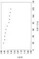
2 is a graph showing the relationship between the elapsed time after the sol solution is applied on a glass substrate by using a bar coater and the weight ratio of the coating film with elapsed time with respect to the dry weight of the coating film.
3 is a conceptual diagram of an apparatus for producing a flexible mold in a roll process.
4 is a flowchart showing a method of manufacturing a substrate having a concavo-convex pattern by heating and pressing.
5 is a conceptual diagram of an apparatus used for carrying out the method of the present invention.
6 is a conceptual diagram of another apparatus used for carrying out the method of the present invention.
7 is a conceptual diagram of an apparatus used for carrying out a method of using heat pressing.
Fig. 8 is a conceptual diagram of another device used to implement a method using heat pressing.
Fig. 9 is a conceptual diagram of another device used to implement a method using heat pressing.
Fig. 10 is a conceptual diagram of another device used to implement a method using heat pressing.
11 is a conceptual diagram of another apparatus used for carrying out the method using the heat pressing.
Fig. 12 is a conceptual diagram of another apparatus used for carrying out a method using heat pressing.
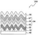
13 is a diagram showing a cross-sectional structure of an organic EL device.
14 (a) is a plan view of a mold, Fig. 14 (b) is a plan view in which one pattern is divided into three parts, Fig. 14 (c) Sectional view of the divided pattern of FIG.
15 is a graph showing the relationship between the elapsed time after coating the sol solution in Example 2 using a spin coater on a glass substrate and the weight ratio of the coating film at elapsed time with respect to the dry weight of the coating film.
16 is a graph showing the relationship between the elapsed time after coating of the sol solution in Example 5 with a spin coater on a glass substrate and the ratio of the weight of the coating film to the elapsed time with respect to the dry weight of the coating film.
이하, 본 발명의 요철 패턴을 가지는 기판의 형성 방법의 실시 형태에 대하여 도면을 참조하면서 설명한다.DESCRIPTION OF THE PREFERRED EMBODIMENTS Hereinafter, embodiments of a method of forming a substrate having a concavo-convex pattern according to the present invention will be described with reference to the drawings.
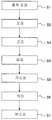
본 발명의 요철 패턴을 가지는 기판의 형성 방법은, 도 1에 나타낸 바와 같이, 주로, 졸 용액(졸겔 용액라고도 함)을 조제하는 용액 조제 단계(S1), 조제된 졸 용액을 기판에 도포하는 도포 단계(S2), 기판에 도포된 졸 용액의 코팅막을 건조시키는 건조 단계(S3), 소정 시간 건조한 코팅막에, 전사 패턴이 형성된 몰드를 가압하는 압압 단계(S4), 몰드가 가압된 코팅막을 가소성(假燒成)하는 가소성 단계(S5), 몰드를 코팅막으로부터 박리하는 박리 단계(S6), 및 코팅막을 본(本)소성하는 본소성 단계(S7)를 가진다. 이하, 각각의 단계에 대하여 차례로 설명한다.As shown in Fig. 1, a method of forming a substrate having a concavo-convex pattern according to the present invention includes a solution preparing step (S1) for preparing a sol solution (also referred to as a sol-gel solution), a coating step A pressing step (S4) of pressing a mold having a transfer pattern on a coating film that has been dried for a predetermined time, a pressing step (S4) of pressing the pressed coating film on the substrate, (S6) for peeling the mold from the coating film, and a final firing step (S7) for firing the coating film. Hereinafter, each step will be described in turn.
[졸 용액 조제 단계][Preparation step of sol solution]
본 발명에서는, 졸겔법에 의해 패턴이 전사되는 코팅막을 형성하기 위해, 최초에 졸 용액을 조제한다. 예를 들면, 기판 위에, 실리카를 졸겔법으로 합성하는 경우에는, 금속 알콕시드(실리카 전구체)의 졸 용액을 조제한다. 실리카의 전구체로서, 테트라메톡시 실란(TMOS), 테트라에톡시 실란(TEOS), 테트라-i-프로폭시 실란, 테트라-n-프로폭시 실란, 테트라-i-부톡시시란, 테트라-n-부톡시 실란, 테트라-sec-부톡시 실란, 테트라-t-부톡시 실란 등의 테트라알콕시드 모노머나; 메틸 트리메톡시 실란, 에틸 트리메톡시 실란, 프로필 트리메톡시 실란, 이소프로필 트리메톡시 실란, 페닐 트리메톡시 실란, 메틸 트리에톡시 실란(MTES), 에틸 트리에톡시 실란, 프로필 트리에톡시 실란, 이소프로필 트리에톡시 실란, 페닐 트리에톡시 실란, 메틸 트리프로폭시 실란, 에틸 트리프로폭시 실란, 프로필 트리프로폭시 실란, 이소프로필 트리프로폭시 실란, 페닐 트리프로폭시 실란, 메틸 트리이소프로폭시 실란, 에틸 트리이소프로폭시 실란, 프로필 트리이소프로폭시 실란, 이소프로필 트리이소프로폭시 실란, 페닐 트리이소프로폭시 실란 등의 트리알콕시드 모노머나; 이들 모노머를 소량 중합한 폴리머, 상기 재료의 일부에 관능기나 폴리머를 도입한 것을 특징으로 하는 복합재료 등의 금속 알콕시드를 들 수 있다. 또한, 금속 아세틸 아세토네이트, 금속 카르복실레이트, 옥시 염화물, 염화물이나, 이들 혼합물 등을 들 수 있지만, 이들에 한정되지 않는다. 또한, 금속종으로서는, Si 이외에 Ti, Sn, Al, Zn, Zr, In 등이나, 이들의 혼합물 등을 들 수 있지만 이들에 한정되지 않는다. 상기 산화 금속의 전구체를 적절히 혼합한 것을 사용할 수도 있다.In the present invention, in order to form a coating film to which a pattern is transferred by the sol-gel method, a sol solution is first prepared. For example, when a silica is synthesized on a substrate by a sol-gel method, a sol solution of a metal alkoxide (silica precursor) is prepared. As precursors of silica, tetramethoxysilane (TMOS), tetraethoxysilane (TEOS), tetra-i-propoxysilane, tetra-n-propoxysilane, tetra-i-butoxy silane, tetra- Butoxy silane, tetra-sec-butoxy silane and tetra-t-butoxy silane; But are not limited to, methyltrimethoxysilane, ethyltrimethoxysilane, propyltrimethoxysilane, isopropyltrimethoxysilane, phenyltrimethoxysilane, methyltriethoxysilane (MTES), ethyltriethoxysilane, propyltriethoxy But are not limited to, silane, isopropyltriethoxysilane, phenyltriethoxysilane, methyltripropoxysilane, ethyltripropoxysilane, propyltripropoxysilane, isopropyltripropoxysilane, phenyltripropoxysilane, methyltriisopropane Trialkoxydimonomers such as foxy silane, ethyl triisopropoxysilane, propyltriisopropoxysilane, isopropyltriisopropoxysilane, and phenyltriisopropoxysilane; A polymer obtained by polymerizing a small amount of these monomers, and a composite material characterized by introducing a functional group or a polymer into a part of the above material. In addition, examples thereof include, but are not limited to, metal acetylacetonate, metal carboxylate, oxychloride, chloride, and mixtures thereof. Examples of the metal species include Si, Ti, Sn, Al, Zn, Zr, In, etc. in addition to Si, and mixtures thereof. A mixture of the precursors of the metal oxides appropriately may be used.
TEOS와 MTES의 혼합물을 사용하는 경우에는, 이들 혼합비는, 예를 들면, 몰비로 1:1로 할 수 있다. 이 졸 용액은 가수분해 및 중축합 반응을 하게 함으로써 비정질 실리카를 생성한다. 합성 조건으로서 용액의 pH를 조정하기 위해, 염산 등의 산 또는 암모니아 등의 알칼리를 첨가한다. pH는 4 이하 또는 10 이상이 바람직하다. 또한, 가수분해를 행하기 위해 물을 첨가해도 된다. 첨가하는 물의 양은 금속 알콕시드종(種)에 대해 몰비로 1.5배 이상으로 할 수 있다.In the case of using a mixture of TEOS and MTES, these mixing ratios can be, for example, 1: 1 in a molar ratio. This sol solution causes hydrolysis and polycondensation reaction to produce amorphous silica. As a synthesis condition, an acid such as hydrochloric acid or an alkali such as ammonia is added to adjust the pH of the solution. The pH is preferably 4 or less or 10 or more. In addition, water may be added for hydrolysis. The amount of water to be added can be 1.5 times or more as a molar ratio to the metal alkoxide species (species).
용매로서는, 예를 들면, 메탄올, 에탄올, 이소프로필 알코올(IPA), 부탄올 등의 알코올류; 헥산, 헵탄, 옥탄, 데칸, 시클로헥산 등의 지방족 탄화수소류; 벤젠, 톨루엔, 크실렌, 메시틸렌 등의 방향족 탄화수소류; 디에틸 에테르, 테트라하이드로 퓨란, 디옥산 등의 에테르류; 아세톤, 메틸 에틸 케톤, 이소포론, 시클로헥사논 등의 케톤류; 부톡시 에틸 에테르, 헥실 옥시 에틸 알코올, 메톡시-2-프로판올, 벤질 옥시 에탄올 등의 에테르 알코올류; 에틸렌 글리콜, 프로필렌 글리콜 등의 글리콜류; 에틸렌 글리콜 디메틸 에테르, 디에틸렌 글리콜 디메틸 에테르, 프로필렌 글리콜 모노메틸 에테르 아세테이트 등의 글리콜 에테르류; 초산 에틸(ethyl acetate), 젖산 에틸(ethyl lactate), γ-부티로락톤 등의 에스테르류; 페놀, 클로로 페놀 등의 페놀류; N,N-디메틸포름아미드, N,N-디메틸아세트 아미드, N-메틸 피롤리돈 등의 아미드류; 클로로포름, 염화 메틸렌, 테트라클로로 에탄, 모노클로로벤젠, 디클로로 벤젠 등의 할로겐계 용매; 이황화 탄소 등의 함(含)헤테로 원소 화합물; 물; 및 이들의 혼합 용매를 들 수 있다. 특히, 에탄올 및 이소프로필 알코올이 바람직하고, 또한 그것들에 물을 혼합한 것도 바람직하다.As the solvent, for example, alcohols such as methanol, ethanol, isopropyl alcohol (IPA) and butanol; Aliphatic hydrocarbons such as hexane, heptane, octane, decane and cyclohexane; Aromatic hydrocarbons such as benzene, toluene, xylene, and mesitylene; Ethers such as diethyl ether, tetrahydrofuran and dioxane; Ketones such as acetone, methyl ethyl ketone, isophorone, and cyclohexanone; Ether alcohols such as butoxyethyl ether, hexyloxyethyl alcohol, methoxy-2-propanol and benzyloxyethanol; Glycols such as ethylene glycol and propylene glycol; Glycol ethers such as ethylene glycol dimethyl ether, diethylene glycol dimethyl ether and propylene glycol monomethyl ether acetate; Esters such as ethyl acetate, ethyl lactate and? -Butyrolactone; Phenols such as phenol and chlorophenol; Amides such as N, N-dimethylformamide, N, N-dimethylacetamide and N-methylpyrrolidone; Halogenated solvents such as chloroform, methylene chloride, tetrachloroethane, monochlorobenzene, and dichlorobenzene; Containing hetero-element compounds such as carbon disulfide; water; And mixed solvents thereof. Particularly, ethanol and isopropyl alcohol are preferable, and it is also preferable to mix them with water.
첨가물로서는, 점도 조정을 위한 폴리에틸렌 글리콜, 폴리에틸렌 옥시드, 하이드록시 프로필 셀룰로오스, 폴리비닐 알코올이나; 용액 안정제인 트리에탄올 아민 등의 알칸올 아민; 아세틸아세톤 등의 β-디케톤, β-케토 에스테르, 포름 아미드, 디메틸 포름 아미드, 디옥산 등의 임의의 첨가제를 사용할 수 있다.Examples of additives include polyethylene glycol, polyethylene oxide, hydroxypropylcellulose, and polyvinyl alcohol for adjusting viscosity; Alkanolamines such as triethanolamine as a solution stabilizer; And any of various additives such as? -Diketone such as acetylacetone,? -Ketoester, formamide, dimethylformamide, dioxane and the like can be used.
또한, 첨가제로서 하기와 같은 계면활성제를 포함해도 된다. 예를 들면, 탄화수소계 계면활성제, 불소계 계면활성제, 실리콘계 계면활성제 등을 들 수 있다. 탄화수소계 계면활성제로서는, 알킬 벤젠 술폰산염계, 고급 알코올 황산 에스테르 염계, 폴리옥시 에틸렌 알킬 에테르 유산염계, α-술포 지방산 에스테르계, α-올레핀 술폰산염계, 모노알킬 인산 에스테르염계, 알칸 술폰산염계, 알킬 트리메틸 암모늄염계, 디알킬 디메틸 암모늄염계, 알킬 디메틸 벤질 암모늄염계, 아민염계, 알킬 아미노 지방산염계, 알킬 아민 옥시드계, 폴리옥시 에틸렌 알킬 에테르계, 폴리옥시 에틸렌 알킬 페놀 에테르계, 알킬 글루코시드계, 폴리옥시 에틸렌 지방산 에스테르계 등을 들 수 있다.As the additive, the following surfactant may be included. Examples thereof include hydrocarbon surfactants, fluorinated surfactants, silicone surfactants and the like. Examples of the hydrocarbon surfactants include alkylbenzenesulfonate salts, higher alcohol sulfate salts, polyoxyethylene alkyl ether sulfate salts,? -Sulfo fatty acid ester salts,? -Olefin sulfonate salts, monoalkyl phosphate ester salts, alkane sulfonate salts, Alkylamines such as ammonium salts, dialkyldimethylammonium salts, alkyldimethylbenzylammonium salts, amine salts, alkylamino fatty acid salts, alkylamine oxides, polyoxyethylene alkyl ethers, polyoxyethylene alkylphenol ethers, alkyl glucosides, Polyoxyethylene fatty acid esters and the like.
[도포 단계][Application step]
상기한 바와 같이 조제한 졸 용액을 기판 위에 도포한다. 기판으로서, 유리나 석영, 실리콘 기판 등의 무기 재료로 이루어지는 기판이나; 폴리에틸렌 테레프탈레이트(PET), 폴리에틸렌 나프탈레이트(PEN), 폴리카보네이트(PC), 시클로올레핀 폴리머(COP), 폴리메틸 메타크릴레이트(PMMA), 폴리스티렌(PS), 폴리이미드(PI), 폴리아릴레이트 등의 수지 기판을 사용할 수 있다. 기판은 투명해도 불투명해도 된다. 이 기판으로부터 얻어진 요철 패턴 기판을 후술하는 유기 EL 소자의 제조에 사용하고 있으면, 기판은 내열성, UV광 등에 대한 내광성을 구비하는 기판이 바람직하다. 이 관점에서, 기판으로서, 유리나 석영, 실리콘 기판 등의 무기 재료로 이루어지는 기판이 더욱 바람직하다. 기판 위에는 밀착성을 향상시키기 위하여, 표면 처리나 이(易)접착층을 형성하는 등을 해도 되고, 수분이나 산소 등의 기체의 침입을 방지하는 목적으로, 가스 배리어층을 형성하는 등을 해도 된다. 도포 방법으로서, 바코팅법, 스핀 코팅법, 스프레이 코팅법, 딥핑(dipping) 코팅법, 다이(die) 코팅법, 잉크젯법 등의 임의의 도포 방법을 이용할 수 있지만, 비교적 대면적의 기판에 졸 용액을 균일하게 도포 가능한 것, 졸 용액이 겔화하기 전에 신속하게 도포를 완료시킬 수 있는 점에서 보면, 바코팅법, 다이 코팅법 및 스핀 코팅법이 바람직하다. 그리고, 후의 단계에서 졸겔 재료층에 의한 원하는 요철 패턴이 형성되므로, 기판 표면(표면 처리나 이접착층이 있는 경우에는 그것들도 포함하여)은 평탄하면 되고, 이 기판 자체는 원하는 요철 패턴을 갖지 않는다.The sol solution prepared as described above is applied onto the substrate. As the substrate, a substrate made of an inorganic material such as glass, quartz, or silicon substrate; (PET), polyethylene naphthalate (PEN), polycarbonate (PC), cycloolefin polymer (COP), polymethylmethacrylate (PMMA), polystyrene (PS), polyimide (PI), polyarylate Or the like can be used. The substrate may be transparent or opaque. If the concavo-convex pattern substrate obtained from this substrate is used in the production of an organic EL device to be described later, the substrate is preferably a substrate having heat resistance and light resistance against UV light. From this viewpoint, as the substrate, a substrate made of an inorganic material such as glass, quartz, or silicon substrate is more preferable. A surface treatment or an adhesive layer may be formed on the substrate in order to improve the adhesion, or a gas barrier layer may be formed for the purpose of preventing intrusion of gas such as moisture or oxygen. As a coating method, any coating method such as a bar coating method, a spin coating method, a spray coating method, a dipping coating method, a die coating method, and an ink jet method can be used. However, A bar coating method, a die coating method and a spin coating method are preferable from the viewpoint that the solution can be uniformly applied and that the application can be completed quickly before the sol solution gels. Then, a desired concave-convex pattern is formed by the sol-gel material layer in a later step, so that the surface of the substrate (including the surface treatment or the adhesive layer if any) is flat and the substrate itself does not have a desired concavo-convex pattern.
[건조 단계][Drying step]
도포 단계 후, 도포한 코팅막(이하, 적절히, "졸겔 재료층"이라고도 함) 중의 용매를 증발시키기 위해 기판을 대기중 또는 감압 하에서 유지한다. 이 유지 시간이 짧으면 코팅막의 점도가 너무 낮아 후속의 전사 단계에서 전사를 할 수 없고, 유지 시간이 길면 전구체의 중합 반응이 너무 진행되어 전사 단계에서 전사를 할 수 없게 된다. 또한, 유지 온도로서, 10∼100℃의 범위에서 일정 온도가 바람직하고, 10∼30℃의 범위에서 일정 온도가 더욱 바람직하다. 유지 온도가 이 범위보다 높으면, 압압 단계 전에 코팅막의 겔화 반응이 급속히 진행하기 때문에 바람직하지 않고, 유지 온도가 이 범위보다 낮으면, 압압 단계 전의 코팅막의 겔화 반응이 늦어, 생산성이 저하해 바람직하지 않다. 이상과 같이, 유지 온도나 유지 시간에 의해 건조 상황이 변화되므로, 건조 단계에서의 유지 조건을 정밀하게 관리할 필요가 있다. 졸 용액을 도포한 후, 용매의 증발이 진행하는 동시에 전구체의 중합 반응도 진행하여, 졸 용액의 점도 등의 물성도 단시간에 변화한다. 용매의 증발량은 졸 용액 조제 시에 사용하는 용매량(졸 용액의 농도)에도 의존한다. 그러므로, 전사에 바람직한 상태를 평가하는 척도가 요구된다.After the application step, the substrate is kept in the air or under reduced pressure to evaporate the solvent in the applied coating film (hereinafter referred to as "sol-gel material layer " If the retention time is short, the viscosity of the coating film is too low to be transferred in the subsequent transfer step. If the retention time is long, the polymerization reaction of the precursor proceeds too much, and the transfer can not be performed in the transfer step. The holding temperature is preferably a constant temperature in the range of 10 to 100 占 폚, and more preferably in the range of 10 to 30 占 폚. When the holding temperature is higher than this range, the gelling reaction of the coating film rapidly proceeds before the pressing step. If the holding temperature is lower than this range, the gelling reaction of the coating film before the pressing step is delayed, . As described above, since the drying condition changes depending on the holding temperature and the holding time, it is necessary to precisely control the holding condition in the drying step. After the sol solution is applied, the evaporation of the solvent proceeds and the polymerization reaction of the precursor proceeds, and the physical properties such as the viscosity of the sol solution also change in a short time. The evaporation amount of the solvent also depends on the amount of solvent (concentration of the sol solution) used in preparing the sol solution. Therefore, a measure for evaluating a desirable state for transcription is required.
본 발명자는 후속의 전사 단계에서의 몰드에 의한 압압을 최적화하기 위해 다음과 같은 관점에서 건조 단계를 관리하는 것으로 하였다. 실리카 전구체의 가수분해·축중합 반응의 경우, 일반적으로, 탈알코올 반응이 일어나기 때문에, 졸 용액 중에 알코올이 생성된다. 또한, 졸 용액 중에는 용매로서 알코올과 같은 휘발성 용매가 사용되고 있다. 즉, 졸 용액 중에는, 가수분해 과정에서 생성한 알코올과, 용매로서 존재한 알코올이 포함되고, 이들을 건조 단계에서 제거함으로써 졸겔 반응이 진행된다. 졸 용액을 유리 기판 위에 바 코터를 사용하여 도포한 후, 용매가 코팅막으로부터 증발할 때의 시간과 증발량을 조사하여 보면, 도 2에 나타낸 바와 같은 결과가 되는 것을 알았다. 즉, 도포 직후부터 용매의 증발이 급속히 시작되어, 지수 함수적으로 증발량이 줄어들고, 소정 시간 후에는 거의 변화하지 않게 된다. 코팅막의 중량이 변화하지 않게 되면, 막 중의 잔존 알코올 용매는 거의 존재하지 않는다고 생각된다. 그러므로, 이때의 코팅막의 중량을 측정함으로써 코팅막 중의 잔존 알코올량을 산출할 수 있고, 그 결과, 졸겔 반응의 진행을 정량화할 수 있다. 코팅막의 중량이 변화하지 않게 될 때의 중량 a에 대해 도포 후 t 시간의 코팅막의 중량을 b(t)로 하여, 전사가 가능해지는 중량 변화 b(t)/a를 구함으로써, 건조 단계의 척도로 할 수 있다. 후술하는 실시예에서 보면, 전구체로서 TEOS와 MTES의 혼합물을 사용하는 경우에는, 패턴을 전사할 수 있는 범위가 1.4≤b(t)/a≤8.8인 것이 바람직하다. b(t)/a가 1.4 미만이면, 코팅막이 단단해져 패턴 전사를 할 수 없다. b(t)/a가 8.8을 넘으면, 용매의 증발이 불충분해 코팅막이 과도하게 유연한 상태이므로, 후속의 전사 단계와 같이 몰드와 코팅막이 접하는 시간이 짧은 경우에는, 몰드를 박리할 때 코팅막 파괴가 일어날 우려가 있든지, 또는 전혀 패턴을 전사할 수 없다. 특히, 후술하는 압압 단계에 있어서 코팅막을 가열하면서 압압하는 경우에는, 건조 단계와 압압 롤을 통과하는 사이의 짧은 시간에 코팅막을 경화시키기 때문에, 건조 단계에 있어서 용매를 충분히 증발시킬 필요가 있는 이유에서, b(t)/a는 1.4≤b(t)/a≤4.5인 것이 바람직하다. 코팅막에 포함되는 용매의 증발이 불충분해 코팅막이 과도하게 유연한 상태이었거나, 또한 b(t)/a가 4.0을 넘으면, 코팅막의 유동성이 높으므로, 패턴 전사 시의 압력으로 액이 전사부 이외로 쉽게 흘러나오게 되어 제조 라인을 오염시킬 가능성이 있으므로, 1.4≤b(t)/a≤4.0인 것이 더욱 바람직하다.The present inventor has managed to manage the drying step in view of the following in order to optimize the pressing by the mold in the subsequent transfer step. In the case of the hydrolysis / condensation polymerization of the silica precursor, alcohol is generally generated in the sol solution because a debOHol reaction occurs. A volatile solvent such as alcohol is used as a solvent in the sol solution. That is, the sol solution contains the alcohol generated in the hydrolysis process and the alcohol present as the solvent, and the sol-gel reaction proceeds by removing them in the drying step. When the sol solution was coated on a glass substrate by using a bar coater, the time and evaporation amount of the solvent evaporated from the coating film were investigated, and the results as shown in Fig. 2 were obtained. That is, the evaporation of the solvent starts rapidly immediately after the application, the amount of evaporation decreases exponentially, and little change occurs after a predetermined time. If the weight of the coating film does not change, it is considered that the remaining alcohol solvent in the film hardly exists. Therefore, by measuring the weight of the coating film at this time, the amount of alcohol remaining in the coating film can be calculated, and as a result, the progress of the sol-gel reaction can be quantified. By determining the weight change b (t) / a in which the transfer is possible, the weight a of the coating film when the weight of the coating film does not change is b (t), the weight of the coating film at time t after coating, . In the examples described below, when a mixture of TEOS and MTES is used as the precursor, it is preferable that the range in which the pattern can be transferred is 1.4? B (t) / a? 8.8. If b (t) / a is less than 1.4, the coating film becomes hard and pattern transfer can not be performed. If b (t) / a exceeds 8.8, the evaporation of the solvent is insufficient and the coating film is in an excessively flexible state. Therefore, when the contact time between the mold and the coating film is short as in the subsequent transferring step, There is a risk of it happening, or you can not transfer the pattern at all. Particularly, in the case of pressing the coating film while heating the coating film in a pressing step to be described later, since the coating film is cured in a short time between the drying step and the pressure roll, it is necessary to sufficiently evaporate the solvent in the drying step , b (t) / a is preferably 1.4? b (t) / a? 4.5. If the coating film is in an excessively flexible state due to insufficient evaporation of the solvent contained in the coating film or b (t) / a exceeds 4.0, the fluidity of the coating film is high, It is more preferable that 1.4? B (t) / a? 4.0 is satisfied because there is a possibility of contaminating the production line.
상기 코팅막의 중량 변화 b(t)/a는, 예비 실험에 의해 도포 후의 졸 용액의 중량 변화를 경과 시간마다 구함으로써 미리 기록하여 둔다. 그리고, 상기 졸 용액의 중량 변화 b(t)/a가 상기 범위에 포함되는 값을 선택하고, 그 값에 상당하는 경과 시간(t)을 건조 단계에서의 유지 시간으로서 설정할 수 있다.The weight change b (t) / a of the coating film is previously recorded by obtaining a change in weight of the sol solution after coating by the elapsed time by a preliminary experiment. Then, a value in which the weight change b (t) / a of the sol solution is included in the above range can be selected, and the elapsed time (t) corresponding to the value can be set as the holding time in the drying step.
[압압 단계][Pressing step]
상기와 같이 하여 설정된 경과 시간 후에, 소정의 미세 요철 패턴이 형성된 몰드를 압압 롤에 의해 코팅막에 가압한다. 압압 롤을 사용한 롤 프로세스에서는, 프레스식과 비교하여 다음과 같은 장점이 있다. i) 몰드와 코팅막이 접하는 시간이 짧으므로, 몰드나 기판 및 기판을 설치하는 스테이지 등의 열팽창계수의 차에 의한 패턴 흐트러짐을 방지할 수 있다. ii) 롤 프로세스이므로, 생산성이 향상되고, 또한 장척의 몰드를 사용함으로써 생산성을 한층 향상시킬 수 있다. iii) 겔 용액 중의 용매의 돌비(突沸)에 의해 패턴 중에 가스의 기포가 발생하거나, 가스 자국이 남는 것을 방지할 수 있다. iv) 기판(코팅막)과 선 접촉하므로, 전사 압력 및 박리력을 줄일 수 있고, 대면적화에 대응하기 쉽다. v) 압압 시에 기포를 포함시키지 않는다.After the elapsed time set as described above, the mold having the predetermined fine concavo-convex pattern formed therein is pressed against the coating film by the pressing roll. In the roll process using the pressing roll, there are the following advantages as compared with the press type. i) Since the contact time between the mold and the coating film is short, it is possible to prevent the pattern from being disturbed by the difference in thermal expansion coefficient between the mold and the stage on which the substrate and the substrate are provided. ii) Since it is a roll process, productivity is improved, and productivity can be further improved by using a long mold. iii) It is possible to prevent gas bubbles from being generated in the pattern due to the boiling of the solvent in the gel solution, or gas marks can be prevented from remaining. iv) Since it is in line contact with the substrate (coating film), the transfer pressure and the peeling force can be reduced, and it is easy to cope with the large-sized. v) Do not include air bubbles when pressing.
압압 롤(전사 롤)은 임의의 것을 사용할 수 있지만, 표면에 에틸렌-프로필렌-디엔 고무(EPDM)나 실리콘 고무, 니트릴 고무, 불소 고무, 아크릴 고무, 클로로프렌 고무 등의 수지 재료의 피막을 가지는 롤이 바람직하다. 또한, 압압 롤에 의해 가해진 압력에 저항하기 위해, 압압 롤에 대향해 기판을 사이에 두도록 한 지지 롤을 설치해도 되고, 또는 기판을 지지하는 지지대를 설치해도 된다.Any roll can be used, and a roll having a film of a resin material such as ethylene-propylene-diene rubber (EPDM), silicone rubber, nitrile rubber, fluorine rubber, acrylic rubber or chloroprene rubber, desirable. Further, in order to resist the pressure applied by the pressing roll, a supporting roll may be provided so as to place the substrate therebetween in opposition to the pressing roll, or a supporting base for supporting the substrate may be provided.
몰드를 압압 롤에 의해 가압할 때, 몰드를 기판의 코팅막 면에 피복하여, 코팅막 면에 서로 마주보고 압압 롤을 회전 이동시킬 수 있다. 또는, 몰드가 압압 롤의 외주에 미리 권취되어 있는 롤을 사용해도 된다. 압압을 할 때, 롤 온도는 10℃∼150℃로 일정하게 유지할 수 있다.When the mold is pressed by the pressing roll, the mold may be coated on the coating film side of the substrate, and the pressing roll may be rotationally moved on the coating film side so as to face each other. Alternatively, a roll in which the mold is previously wound on the outer periphery of the pressing roll may be used. When the pressure is applied, the roll temperature can be kept constant at 10 ° C to 150 ° C.
압압 롤을 사용하여 몰드를 코팅막에 가압할 때, 코팅막을 가열하면서 몰드를 코팅막에 가압해도 된다(적절히, "가열 압압"이라고 함). 코팅막을 가열하면서 몰드를 코팅막에 가압됨으로써, 필름을 접합하는 반대 측으로부터, 가열에 의해 발생하는 가스가 코팅막과 필름의 사이에 머무르지 않고 시스템 밖으로 도피할 수 있어 보이드(void)가 쉽게 생기지 않는다는 효과가 있다. 또한, 가열 압압에 의해, 몰드의 압압에서부터 박리까지의 시간을 단축할 수 있는 동시에, 후술하는 가소성 단계를 압압 단계에서 실행할 수 있다(즉, 가소성 단계를 생략할 수도 있다). 코팅막을 가열하는 방법으로서, 예를 들면, 가열을 압압 롤을 통해 행해도 되거나, 코팅막을 직접 또는 기판 측으로부터 가열해도 된다. 가열을 압압 롤을 통해 행하는 경우에는, 압압 롤(전사 롤)의 내부에 가열 수단을 설치해도 되고, 임의의 가열 수단을 사용할 수 있다. 압압 롤의 내부에 가열 히터를 구비하는 것이 바람직하지만, 압압 롤과는 별개의 히터를 구비하고 있어도 된다. 어쨌든 코팅막을 가열하면서 압압이 가능하면, 어떠한 압압 롤을 사용해도 된다.When the mold is pressed onto the coating film by using the pressing roll, the mold may be pressed against the coating film while heating the coating film (appropriately referred to as "heat pressing"). Since the mold is pressed against the coating film while heating the coating film, the gas generated by the heating can escape from the system without staying between the coating film and the film from the side opposite to the side where the film is adhered, . Further, the time from the pressing to the peeling of the mold can be shortened by heating and pressing, and at the same time, the plasticizing step to be described later can be carried out in the pressing step (that is, the plasticizing step may be omitted). As a method of heating the coating film, for example, heating may be performed through a pressing roll, or the coating film may be heated directly or from the substrate side. When the heating is performed through the pressing roll, heating means may be provided inside the pressing roll (transfer roll), or arbitrary heating means may be used. It is preferable that a heating heater is provided inside the pressing roll, but a heater separate from the pressing roll may be provided. However, any pressure roll may be used as long as the pressure can be applied while heating the coating film.
가열 압압 시의 코팅막의 가열 온도는 40℃∼150℃로 할 수 있고, 압압 롤을 사용하여 가열하는 경우에는 압압 롤의 가열 온도는, 마찬가지로 40℃∼150℃로 할 수 있다. 이와 같이 압압 롤을 가열함으로써, 몰드에 의해 압압을 한 코팅막으로부터 몰드를 바로 박리할 수 있어, 생산성을 향상시킬 수 있다. 코팅막 또는 압압 롤의 가열 온도가, 40℃ 미만에서는 코팅막으로부터의 몰드의 신속한 박리를 기대할 수 없고, 150℃를 넘으면 사용하는 용매가 급격하게 증발하고, 요철 패턴의 전사가 불충분해질 우려가 있다. 그리고, 압압 롤의 아래에 구비하는(후술하는) 지지 롤 도, 예를 들면 40∼150℃로 가열해도 된다. 그리고, 코팅막을 가열하는 수단으로서 압압 롤을 가열할 뿐 아니라 후술하는 바와 같은 다양한 구체적 형태를 채용할 수 있다.The heating temperature of the coating film under heating and pressing can be 40 to 150 占 폚. When heating is performed using a pressing roll, the heating temperature of the pressing roll can be set to 40 to 150 占 폚 in the same manner. By heating the pressure roll in this way, the mold can be directly peeled off from the coating film pressed by the mold, and productivity can be improved. If the heating temperature of the coating film or the pressing roll is less than 40 ° C, rapid release of the mold from the coating film can not be expected. If the heating temperature exceeds 150 ° C, the solvent used may evaporate rapidly, and the transfer of the concavo-convex pattern may become insufficient. The supporting roll (to be described later) provided under the pressing roll may also be heated to, for example, 40 to 150 占 폚. As the means for heating the coating film, not only the pressing roll is heated but also various concrete forms as described later can be adopted.
[압압 단계에서 사용하는 몰드와 그 제조 방법][Mold used in the pressing step and its manufacturing method]
본 발명에서 사용하는 몰드란, 필름형 몰드와 같이 가요성이 있는 몰드를 의미한다. 예를 들면, 실리콘 수지, 폴리에틸렌 테레프탈레이트(PET), 폴리에틸렌 나프탈레이트(PEN), 폴리카보네이트(PC), 시클로올레핀 폴리머(COP), 폴리메틸 메타크릴레이트(PMMA), 폴리스티렌(PS), 폴리이미드(PI), 폴리아릴레이트와 같은 유기 재료나; 니켈, 동, 알루미늄과 같은 금속 재료나; 유리와 같은 무기 재료 등으로 형성되지만, 재료는 한정되지 않고, 임의의 재료의 것을 사용할 수 있다. 또한, 요철 패턴은 상기 재료에 직접 형성되어 있어도 되고, 상기 재료를 기재로 하여 또 다른 재료로 형성해도 된다. 다른 재료로서는, 광경화성 수지나, 열경화성 수지, 열가소성 수지를 사용할 수 있다. 기재와 다른 재료 사이에는, 밀착성을 높이기 위해 표면 처리나 이(易)접착 처리를 행해도 된다. 또한, 필요에 따라, 이들 요철 패턴면 위에 이형 처리를 행해도 된다. 몰드에 형성하는 패턴은, 임의의 형상을 임의의 방법으로 형성할 수 있다. 그리고, 전술한 가열 압압을 행하는 경우에는, 가열 온도에 견딜 수 있는 재료로 형성된 몰드를 사용할 수 있다.The mold used in the present invention means a mold having flexibility such as a film mold. For example, a silicone resin, a polyethylene terephthalate (PET), a polyethylene naphthalate (PEN), a polycarbonate (PC), a cycloolefin polymer (COP), polymethylmethacrylate (PMMA), polystyrene (PS) (PI), polyarylate; Metal materials such as nickel, copper and aluminum; An inorganic material such as glass, and the like, but the material is not limited and any material can be used. The uneven pattern may be formed directly on the material, or may be formed of another material using the material as a base. As other materials, a photo-curable resin, a thermosetting resin, and a thermoplastic resin can be used. Between the base material and another material, a surface treatment or an easy adhesion treatment may be performed to improve the adhesion. If necessary, a mold releasing treatment may be performed on these uneven pattern surfaces. The pattern to be formed on the mold can be formed into an arbitrary shape by an arbitrary method. In the case of carrying out the above-described heating and pressing, a mold formed of a material which can withstand the heating temperature can be used.
유기 EL용 회절 격자 기판에 사용하는 경우에는, 예를 들면, 본 출원인 등에 의한 특허출원 제2011-006487호에 기재된 블록 공중합체의 자체 조직화(마이크로 상분리, mcrophase separation)를 이용하는 방법(이하, 적절히 "BCP(Block Copolymer) 법"이라고 함)이나, 본 출원인등에 의한 WO2011/007878 A1에 개시된 증착막 위의 폴리머막을 가열·냉각함으로써 폴리머 표면의 주름에 의한 요철을 형성하는 방법(이하, 적절히 "BKL(Buckling)법"이라고 함)을 사용하는 것이 바람직하다. BCP법 및 BKL법 대신에, 포토리소그래피법으로 형성해도 된다. BCP법으로 패턴을 형성하는 경우, 패턴을 형성하는 재료는 임의의 재료를 사용할 수 있지만, 폴리스티렌과 같은 스티렌계 폴리머; 폴리메틸 메타크릴레이트와 같은 폴리 알킬 메타크릴레이트; 폴리에틸렌 옥시드, 폴리부타디엔, 폴리이소프렌, 폴리비닐 피리딘, 및 폴리락트산으로 이루어지는 군으로부터 선택되는 2종의 조합으로 이루어지는 블록 공중합체가 바람직하다.In the case of use in a diffraction grating substrate for an organic EL, for example, a method (self-organizing method) using self-organization (mcrophase separation) of a block copolymer described in Patent Application No. 2011-006487 by the present applicant (Hereinafter referred to as " BCP (Block Copolymer) Method ") or by a method of heating and cooling the polymer film on the vapor deposition film disclosed in WO2011 / 007878 A1 by the present applicant or the like to form concave- ) Method ") is preferably used. Instead of the BCP method and the BKL method, a photolithography method may be used. When a pattern is formed by the BCP method, any material can be used as a material for forming the pattern, but a styrenic polymer such as polystyrene; Polyalkyl methacrylates such as polymethyl methacrylate; A block copolymer comprising a combination of two kinds selected from the group consisting of polyethylene oxide, polybutadiene, polyisoprene, polyvinylpyridine, and polylactic acid is preferable.
몰드의 미세 패턴의 요철의 피치 및 높이는 임의이지만, 예를 들면, 가시 영역의 광을 산란 또는 회절시키는 용도로 전사 패턴을 사용하는 경우에는, 요철의 평균 피치로서는, 100∼900㎚, 특히 100∼600㎚ 또는 200∼900㎚의 범위에 있는 것이 바람직하고, 200∼600㎚의 범위인 것이 더욱 바람직하다. 요철의 평균 피치가 상기 하한 미만에서는, 가시광의 파장에 대하여 피치가 너무 작아지므로, 요철에 의한 광의 회절이 생기지 않게 되는 경향이 있고, 다른 한편, 상한을 넘으면, 회절각이 작아져, 회절 격자와 같은 광학 소자로서의 기능을 잃어 버리는 경향이 있다. 요철의 평균 높이는 20∼200㎚의 범위인 것이 바람직하고, 50∼150㎚의 범위인 것이 더욱 바람직하다. 요철의 평균 높이가 상기 하한 미만에서는, 가시광의 파장에 대하여 높이가 너무 낮기 때문에 필요한 회절이 생기지 않게 되는 경향이 있고, 다른 한편, 상한을 넘으면, 예를 들면, 유기 EL 소자의 광인출용의 광학 소자로서 사용한 경우에, EL층 내부의 전계 분포가 불균일하게 되어 특정한 개소(箇所)에 전계가 집중됨으로써 누설(leak)이 쉽게 생기게 되거나, 수명이 짧아지는 경향이 있다.For example, when a transfer pattern is used for scattering or diffracting light in the visible region, the average pitch of the concavities and convexities is preferably 100 to 900 nm, more preferably 100 to 900 nm, 600 nm or 200 to 900 nm, and more preferably 200 to 600 nm. When the average pitch of the concavities and convexities is less than the lower limit, the pitch becomes too small with respect to the wavelength of the visible light, so that the light diffraction due to the unevenness tends not to occur. On the other hand, when the average pitch exceeds the upper limit, The function as the same optical element tends to be lost. The average height of the unevenness is preferably in the range of 20 to 200 nm, more preferably in the range of 50 to 150 nm. When the average height of the concavities and convexities is less than the above lower limit, since the height is too low with respect to the wavelength of the visible light, necessary diffraction tends not to occur. On the other hand, when the average height exceeds the upper limit, When used as an element, the electric field distribution inside the EL layer becomes nonuniform, and the electric field is concentrated at a specific point (location), so that leakage tends to occur easily or the life is shortened.
패턴의 모형(母型)을 BCP법이나 BKL법에 의해 형성한 후, 다음과 같이 하여 전기 주조법(電氣鑄造法) 등에 의해, 패턴을 더 전사한 몰드를 형성할 수 있다. 최초에, 전기 주조 처리를 위한 도전층되는 시드층(seed layer)을, 무전해 도금, 스퍼터 또는 증착 등에 의해 패턴을 가지는 모형 위에 형성할 수 있다. 시드층은 후속의 전기 주조 단계에서의 전류 밀도를 균일하게 하여 후속의 전기 주조 단계에 의해 퇴적되는 금속층의 두께를 일정하게 하기 위해 10㎚ 이상이 바람직하다. 시드층의 재료로서, 예를 들면, 니켈, 동, 금, 은, 백금, 티탄, 코발트, 주석, 아연, 크롬, 금·코발트 합금, 금·니켈 합금, 붕소·니켈 합금, 땜납, 동·니켈·크롬 합금, 주석 니켈 합금, 니켈·팔라듐 합금, 니켈·코발트·인 합금, 또는 이들 합금 등을 사용할 수 있다. 다음에, 시드층 상에 전기 주조(전계 도금)에 의해 금속층을 퇴적시킨다. 금속층의 두께는, 예를 들면, 시드층의 두께를 포함하여 전체로 10∼3000㎛의 두께로 할 수 있다. 전기 주조에 의해 퇴적시키는 금속층의 재료로서, 시드층으로서 사용할 수 있는 상기 금속종 중 어느 하나를 사용할 수 있다. 금속 기판의 몰드로서의 내마모성이나, 박리성 등의 관점에서는, 니켈이 바람직하고, 이 경우, 시드층에 대해도 니켈을 사용하는 것이 바람직하다. 형성한 금속층은 후속의 몰드의 형성을 위한 수지층의 가압, 박리 및 세정 등의 처리의 용이성의 점에서, 적절한 경도 및 두께를 가지는 것이 바람직하다.After the pattern of the pattern is formed by the BCP method or the BKL method, a mold may be formed by further transferring the pattern by an electroforming method or the like as follows. First, a seed layer to be a conductive layer for an electroforming process can be formed on a pattern having a pattern by electroless plating, sputtering, vapor deposition or the like. The seed layer is preferably 10 nm or more in order to make the current density at the subsequent electroforming step uniform and to make the thickness of the metal layer deposited by the subsequent electroforming step uniform. As the material of the seed layer, for example, a metal such as nickel, copper, gold, silver, platinum, titanium, cobalt, tin, zinc, chromium, gold-cobalt alloy, gold-nickel alloy, Chromium alloys, tin nickel alloys, nickel-palladium alloys, nickel-cobalt-phosphorus alloys, and alloys thereof. Next, a metal layer is deposited on the seed layer by electroforming (electric plating). The thickness of the metal layer can be, for example, 10 to 3000 占 퐉 as a whole including the thickness of the seed layer. As the material of the metal layer to be deposited by electroforming, any of the above metal species that can be used as the seed layer can be used. Nickel is preferable from the viewpoints of abrasion resistance as a mold of the metal substrate, peelability, etc. In this case, it is preferable to use nickel for the seed layer. The formed metal layer preferably has appropriate hardness and thickness in terms of easiness of processing such as pressing, peeling and cleaning of the resin layer for forming a subsequent mold.
상기와 같이 하여 얻어진 시드층을 포함하는 금속층을, 요철 구조를 가지는 모형으로부터 박리하여 금속 기판을 얻는다. 박리 방법은 물리적으로 벗겨도 상관없고, 패턴을 형성하는 재료를, 그것들을 용해하는 유기용매, 예를 들면, 톨루엔, 테트라하이드로 퓨란(THF), 클로로포름 등을 사용하여 용해하여 제거해도 된다. 금속 기판을 모형으로부터 박리할 때, 잔류하고 있는 재료 성분을 세정에 의해 제거할 수 있다. 세정 방법으로서는, 계면활성제 등을 사용한 습식 세정이나 자외선이나 플라즈마를 사용한 건식 세정을 사용할 수 있다. 또한, 예를 들면, 점착제나 접착제를 사용하여 잔류하고 있는 재료 성분을 부착 제거하는 등을 해도 된다. 이와 같이 하여 모형으로부터 패턴이 전사된 금속 기판을 얻을 수 있다.The metal layer including the seed layer thus obtained is peeled off from the model having the concavo-convex structure to obtain a metal substrate. The peeling method may be physically peeled off, and the material forming the pattern may be removed by dissolving them using an organic solvent dissolving them, for example, toluene, tetrahydrofuran (THF), chloroform or the like. When the metal substrate is peeled from the model, the remaining material components can be removed by cleaning. As the cleaning method, wet cleaning using a surfactant or the like or dry cleaning using ultraviolet rays or plasma can be used. Further, for example, a residual material component may be removed by adhesion using a pressure-sensitive adhesive or an adhesive. In this manner, a metal substrate onto which a pattern is transferred from the pattern can be obtained.
이 금속 기판을 사용하여, 금속 기판의 요철 구조(패턴)를 필름형의 지지 기판에 전사함으로써 필름형 몰드와 같이 가요성이 있는 몰드를 제작할 수 있다. 예를 들면, 경화성 수지를 지지 기판에 도포한 후, 금속 기판의 요철 구조를 수지층에 가압하면서 수지층을 경화시킨다. 지지 기판으로서, 예를 들면, 유리 등의 무기 재료로 이루어지는 기재; 실리콘 수지, 폴리에틸렌 테레프탈레이트(PET), 폴리에틸렌 나프탈레이트(PEN), 폴리카보네이트(PC), 시클로올레핀 폴리머(COP), 폴리메틸 메타크릴레이트(PMMA), 폴리스티렌(PS), 폴리이미드(PI), 폴리아릴레이트 등의 유기 재료로 이루어지는 기재; 니켈, 동, 알루미늄 등의 금속 재료를 들 수 있다. 또한, 지지 기판의 두께는, 1∼500㎛의 범위로 할 수 있다.By using this metal substrate and transferring the concavo-convex structure (pattern) of the metal substrate to the film-like support substrate, it is possible to produce a flexible mold like the film-type mold. For example, after a curable resin is applied to a support substrate, the resin layer is cured while pressing the concavo-convex structure of the metal substrate against the resin layer. As the supporting substrate, for example, a substrate made of an inorganic material such as glass; (PET), polyethylene naphthalate (PEN), polycarbonate (PC), cycloolefin polymer (COP), polymethylmethacrylate (PMMA), polystyrene (PS), polyimide (PI) A substrate made of an organic material such as polyarylate; Nickel, copper, and aluminum. The thickness of the supporting substrate may be in the range of 1 to 500 mu m.
경화성 수지로서는, 예를 들면, 에폭시계, 아크릴계, 메타크릴계, 비닐 에테르계, 옥세탄계, 우레탄계, 멜라민계, 우레아계, 폴리에스테르계, 페놀계, 가교형(架橋型) 액정계, 불소계, 실리콘계 등의 각종 수지를 들 수 있다. 경화성 수지의 두께는 0.5∼500㎛의 범위인 것이 바람직하다. 두께가 상기 하한 미만에서는, 경화 수지층의 표면에 형성되는 요철의 높이가 불충분해지고 쉽고, 상기 상한을 넘으면, 경화 시에 생기는 수지의 체적 변화의 영향이 커져 요철 형상을 양호하게 형성할 수 없게 될 가능성이 있다.Examples of the curable resin include epoxy, acrylic, methacrylic, vinyl ether, oxetane, urethane, melamine, urea, polyester, phenol, Silicone, and the like. The thickness of the curable resin is preferably in the range of 0.5 to 500 mu m. If the thickness is less than the lower limit described above, the height of the irregularities formed on the surface of the cured resin layer becomes insufficient, and if the thickness exceeds the upper limit, the influence of the volume change of the resin caused upon curing becomes large, There is a possibility.
경화성 수지를 도포하는 방법으로서는, 예를 들면, 스핀 코팅법, 스프레이 코팅법, 딥 코팅법, 적하법, 그라비아 인쇄법, 스크린 인쇄법, 철판(凸版) 인쇄법, 다이 코팅법, 커텐 코팅법, 잉크젯법, 스퍼터법 등의 각종 코팅 방법을 채용할 수 있다. 또한, 경화성 수지를 경화시키는 조건으로서는, 사용하는 수지의 종류에 따라 상이하지만, 예를 들면, 경화 온도가 실온∼250℃의 범위이며, 경화 시간이 0.5분∼3시간의 범위인 것이 바람직하다. 또한, 자외선이나 전자선과 같은 에너지선을 조사함으로써 경화시키는 방법이어도 되고, 그 경우에는, 조사량은 20mJ/cm2∼5 J/cm2의 범위인 것이 바람직하다.Examples of the method of applying the curable resin include a spin coating method, a spray coating method, a dip coating method, a dropping method, a gravure printing method, a screen printing method, an iron plate printing method, a die coating method, Various coating methods such as an ink jet method and a sputtering method may be employed. The conditions for curing the curable resin differ depending on the type of the resin to be used. For example, it is preferable that the curing temperature is in the range of room temperature to 250 캜, and the curing time is in the range of 0.5 minutes to 3 hours. In addition, it may be a method of curing by irradiating energy rays such as ultraviolet rays or electron beams. In this case, the irradiation dose is preferably inthe range of 20 mJ / cm2 to 5 J / cm2 .
이어서, 경화 후의 경화 수지층으로부터 금속 기판을 분리한다. 금속 기판을 분리하는 방법으로서는, 기계적인 박리법에 한정되지 않고, 공지의 방법을 채용할 수 있다. 이와 같이 하여 지지 기판 위에 요철이 형성된 경화 수지층을 가지는 수지 필름으로 이루어지는 몰드를 얻을 수 있다.Subsequently, the metal substrate is separated from the cured resin layer after curing. The method for separating the metal substrate is not limited to the mechanical peeling method, but a known method can be employed. In this manner, a mold made of a resin film having a cured resin layer having concavities and convexities on the support substrate can be obtained.
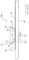
금속 기판을 사용하여 필름형 몰드와 같이 가요성이 있는 몰드를 제작하는 롤프로세스의 일례를 도 3에 나타낸다. 도 3에 나타낸 롤 프로세스 장치(70)는, PET와 같은 기판 필름(80)의 반송 시스템과, 반송 중의 기판 필름(80)에 UV 경화성 수지를 도포하는 다이 코터(82)와, 다이 코터(82)의 하류 측에 위치하여 패턴을 전사하는 금속 롤(금속 몰드)(90)과, 기판 필름(80)을 사이에 두고 금속 롤(90)과 대향하여 설치되어 기판 필름(80)에 UV 광을 조사하는 조사 광원(85)을 주로 구비한다. 금속 롤(90)은, 금속 롤 표면에 직접 패턴이 형성된 것이어도 되고, 상기 금속 기판을 롤 위에 감아 고정한 것이어도 되고, 또한, 원통형의 금속 기판을 제작하고, 이것을 롤에 끼워넣어 고정한 것 등이어도 된다. 반송 시스템은 기판 필름(80)을 송출하는 필름 송출 롤(72)과, 금속 롤(90)의 상류 및 하류 측에 각각 배치되어 기판 필름을 금속 롤(90)에 부세(付勢)하는 닙롤(nip roll)(74)과, 박리 롤(76)과, 패턴이 전사된 기판 필름(80)을 권취하는 권취 롤(78)을 가진다. 필름 송출 롤(72)에 권취된 기판 필름(80)은 필름 송출 롤(80)의 회전에 의해 하류 측에 송출되면 다이 코터(82)에 의해 UV 경화성 수지(84)가 기판 필름(80)의 상면에 소정의 두께로 도포된다. 이 기판 필름(80)의 UV 경화성 수지(84)에 닙롤(74)에 의해 금속 롤(90)이 가압되어 금속 롤(90)의 요철 패턴이 전사되고, 그와 동시 또는 그 직후에 조사 광원(85)으로부터의 UV 광이 조사되어 UV 경화성 수지(84)가 경화된다. 경화한 패턴을 가지는 UV 경화성 수지 부가 기판 필름(87)은 박리 롤(76)에 의해 금속 롤(90)로부터 떼어진 후, 권취 롤(78)에 의해 권취된다. 이와 같이 하여, 장척의 가요성이 있는 몰드를 얻을 수 있다. 이와 같은 장척의 몰드는, 본 발명에 따르는 압압 롤을 사용한 전사 프로세스(나노 임프린트)에 적합하게 된다.An example of a roll process for producing a flexible mold such as a film-type mold using a metal substrate is shown in Fig. The
[가소성 단계][Step of plasticity]
코팅막(졸겔 재료층)에 몰드를 가압한 후, 코팅막을 가소성해도 된다. 가소성함으로써 코팅막의 겔화를 진행시켜, 패턴을 고화(固化)하고, 박리 시에 쉽게 흐트러지지 않게 한다. 가소성을 행하는 경우에는, 대기중에서 40∼150℃의 온도로 가열하는 것이 바람직하다. 그리고, 가소성은 반드시 행할 필요는 없다. 그리고, 도 4에 압압 단계에서 가열 압압을 행하는 경우의 프로세스를 나타낸다.After the mold is pressed onto the coating film (sol-gel material layer), the coating film may be calcined. The gelation of the coating film is promoted by baking, and the pattern is solidified, so that it is not easily disturbed at the time of peeling. In the case of performing the plasticity, it is preferable to heat it to 40 to 150 DEG C in the air. The plasticity is not necessarily required. Fig. 4 shows a process in the case of performing heating and pressing in the pressing step.
[박리 단계][Peeling step]
압압 단계 또는 가소성 단계 후의 코팅막(졸겔 재료층)으로부터 몰드를 박리한다. 전술한 바와 같이 롤을 사용하므로, 플레이트형 몰드에 비해 박리력은 작아도 되고, 코팅막이 몰드에 잔류하지 않고 용이하게 몰드를 코팅막으로부터 박리할 수 있다. 또한, 몰드의 박리를 촉진하기 위해, 후술하는 박리 롤을 사용할 수 있다(도 5 참조). 박리 롤을 압압 롤의 하류 측에 설치하여 몰드를 코팅막에 부세하면서 회전 지지함으로써, 몰드가 코팅막에 부착된 상태를 일정 시간 유지할 수 있고, 그 유지 기간에 전술한 코팅막의 가소성을 행할 수 있다. 또한, 박리 롤을 사용함으로써, 박리 부분이 순차적으로 이동하기 때문에 박리력이 작아도 되고, 한번에 몰드를 박리하는 경우에 비해, 패턴의 흐트러짐이 적어진다. 그리고, 박리 롤을 예를 들면 40∼150℃로 가열하면서 박리함으로써 코팅막의 박리를 한층 용이하게 할 수 있다.The mold is peeled off from the coating film (sol-gel material layer) after the pressing step or the plasticizing step. As described above, since the roll is used, the peeling force can be smaller than that of the plate mold, and the mold can be easily peeled from the coating film without the coating film remaining on the mold. Further, in order to promote the peeling of the mold, a peeling roll described later can be used (see Fig. 5). By providing the peeling roll on the downstream side of the pressing roll and rotating the mold while pressing the mold against the coating film, the state that the mold is adhered to the coating film can be maintained for a certain period of time, and the above-described coating film can be plasticized during the holding period. Further, by using the peeling roll, the peeling force can be small because the peeling section moves sequentially, and the pattern disturbance is reduced as compared with the case where the mold is peeled at one time. Then, the peeling roll is peeled while being heated, for example, at 40 to 150 캜, whereby the peeling of the coating film can be further facilitated.
[본소성 단계][The step of sintering]
기판(40)의 코팅막(졸겔 재료층)(42)으로부터 몰드가 박리된 후, 코팅막을 본소성한다. 본소성에 의해 코팅막을 구성하는 실리카(비정질 실리카) 중에 포함되어 있는 수산기 등이 이탈하여 코팅막이 더욱 강고(强固)해진다. 본소성은 200∼1200℃의 온도로, 5분∼6시간 정도 행하는 것이 좋다. 이와 같이 하여 코팅막은 경화되어 몰드의 요철 패턴에 대응하는 요철 패턴막을 가지는 기판, 즉 평탄한 기판 위에 요철 패턴을 가지는 졸겔 재료층이 직접 형성된 기판을 얻을 수 있다. 이때, 졸겔 재료층인 실리카는 소성 온도, 소성 시간에 따라 비정질 또는 결정질, 또는 비정질과 결정질의 혼합 상태가 된다.After the mold is peeled from the coating film (sol-gel material layer) 42 of the
[제조 장치][Manufacturing apparatus]
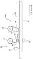
본 발명의 방법을 실시하기 위해, 예를 들면, 도 5에 나타낸 바와 같은 요철 패턴 부가 기판을 제조하는 장치(100a)를 사용할 수 있다. 장치(100a)는, 주로, 기판(40) 상에 졸 용액을 도포하는 다이 코터(30)와, 장척형의 몰드(50)를 반송하는 반송 시스템(20)과, 코팅막을 가열하는 히터(32)를 구비한다. 반송 시스템(20)은 몰드(50)를 송출하는 송출 롤(21)과, 코팅막(42)이 형성된 기판(40)의 코팅막 측에서 몰드(50)를 가압하는 압압 롤(22)과, 압압 롤(22)에 대향하여 설치되어 기판 아래쪽으로부터 기판(40)을 압합하는 동시에 회전 구동하여 기판을 기판 반송 방향의 하류 측에 송출하는 지지 롤(25)과, 압압 롤(22)의 하류에 설치되어 몰드(50)가 기판의 코팅막에 가압된 상태를 소정 거리만큼 유지한 후에 몰드(50)를 박리하는 박리 롤(23)과, 박리 롤의 하류에 설치되어 몰드를 권취하는 권취 롤(24)을 가진다. 히터(32)는 가소성용 히터이며, 기판 반송 방향에 있어서 압압 롤(22)과 박리 롤(23) 사이에 위치한다. 히터(32)는, 예를 들면, 적외선 히터나 열풍 가열, 핫 플레이트를 사용할 수 있다.In order to carry out the method of the present invention, for example, an
이와 같은 장치(100a)로, 기판을 처리하는 동작을 설명한다. 압압 롤(22)과 지지 롤(25)에 끼워진 기판(40)이 하류 측으로 이동하면서, 다이 코터(30)에 의해 기판(40)에 졸 용액이 도포된다. 도포된 졸 용액의 코팅막(42)은, 소정의 이동 시간 경과 후에 압압 롤(22)에 도달하고, 그곳에서 송출 롤(21)로부터 송출된 몰드(50)의 요철 패턴이 코팅막(42)에 가압된다. 기판(40)은, 몰드(50)의 요철 패턴이 가압된 채 반송되어 히터(32)의 위쪽을 통과할 때 코팅막(42)은 가소성된다. 몰드(50)는 박리 롤(23)을 통과할 때 권취 롤(24)에 의해 위쪽으로 끌어 올려지므로, 몰드(50)는 코팅막(42)으로부터 박리한다. 이어서, 패턴이 형성된 기판을 장치(100a)와는 별도로 설치한 오븐에서 본소성한다. 또한, 본소성용 오븐으로서는 라인 중에 히터를 설치해도 된다.An operation of processing the substrate with such an
장치(100a)에 있어서, 박리 롤(23)의 설치 위치나, 박리 롤(23)을 개재시켜 몰드를 권취하는 권취 롤(24)의 위치를 조절하여 박리 각도를 조정해도 된다. 그리고, 히터(32)는, 기판(40)에 대해 코팅막(42) 측에 설치해도 되고, 지지 롤(25) 대신에, 기판을 지지하여 이동하는 이동 테이블 등의 다른 구동 수단을 사용할 수 있다. 또한, 히터(32)에 의해 코팅막(42)이 가소성되는 동안, 압압 롤(22)에 의해 몰드(50)의 요철 패턴이 코팅막(42)에 가압된 그대로의 상태를 유지하기 위해 박리 롤(23)을 사용하였지만, 그와 같은 상태를 유지하기 위해 박리 롤(23) 대신에, 표면이 매끄럽고 코너부가 곡면을 가지는 판형 부재 등의 다른 지지 부재를 사용할 수 있다. 또한, 몰드(50)는 장척형의 몰드로서, 단부(端部)를 각각 송출 롤(21) 및 권취 롤(24)에 권취하였으나, 도 6에 나타낸 장치(100b)와 같이 무단(無端) 벨트형로 해도 된다. 이렇게 함으로써, 양산을 위해 다량의 기판이 연속 반송되는 라인에 있어서도 연속적인 압압 조작이 가능해진다.The peeling angle may be adjusted by adjusting the installation position of the peeling
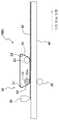
압압 단계에서 가열 압압을 행하는 경우에 사용하는 장치의 일례를 도 7에 나타낸다. 도 7에 나타낸 장치(100c)는, 기본적으로는, 압압 롤(22)이 그 내부에 가열 히터(22a)를 구비하는 것 외에는, 도 3에 나타낸 장치(100a)와 같은 구조를 가진다. 기판 반송 방향에 있어서 압압 롤(22)과 박리 롤(23) 사이에, 도 3에 나타낸 바와 같은 히터(33)를 설치해도 되지만, 압압 롤(22)이 가열 히터(22a)를 구비하기 때문에, 히터(33)는 생략할 수 있다. 이 장치(100c)에서는, 도포된 졸 용액의 코팅막(42)은 소정의 이동 시간 경과 후에 가열 압압 롤(22)에 도달하고, 그곳에서 송출 롤(21)로부터 송출된 몰드(50)의 요철 패턴이 가열되면서 코팅막(42)에 가압된다.Fig. 7 shows an example of a device used when heating and pressing in the pressing step is performed. The
장치(100c)에 있어서, 박리 롤(23)의 설치 위치나, 박리 롤(23)을 개재시켜 몰드를 권취하는 권취 롤(24)의 위치를 조절하여 박리 각도를 조정해도 된다. 그리고, 지지 롤(25) 대신에, 기판을 지지하여 이동하는 이동 테이블 등의 다른 구동 수단을 사용할 수 있다. 또한, 압압 롤(22)에 의해 몰드(50)의 요철 패턴이 코팅막(42)에 가압된 그대로의 상태를 유지하기 위해 박리 롤(23)을 사용하였지만, 그와 같은 상태를 유지하기 위해 박리 롤(23) 대신에, 표면이 매끄럽고 코너부가 곡면을 가지는 판형 부재 등의 다른 지지 부재를 사용할 수 있다. 또한, 몰드(50)는 장척형의 몰드로서, 단부를 각각 송출 롤(21) 및 권취 롤(24)에 권취하였으나, 도 8에 나타낸 장치(100d)와 같이, 무단 벨트형으로 해도 된다. 이렇게 함으로써, 양산을 위해 다량의 기판이 연속 반송되는 라인에 있어서도 연속적인 압압 조작이 가능해진다.The peeling angle may be adjusted by adjusting the installation position of the peeling
박리 롤을 설치하지 않는 장치의 일례를 도 9에 나타낸다. 도 9에 나타낸 장치(100e)에서는, 송출 롤(26)로부터 송출된 몰드(50)가 가열 압압 롤(22)로 코팅막(42)에 압압(押壓)된 후에, 직접, 권취 롤(27)에 의해 감아 올려져 주회(周回)한다. 본 발명에서는, 압압 롤을 가열하고 있으므로, 압압 직후의 몰드의 코팅막으로부터의 박리가 촉진되어 있어, 박리 롤을 생략하여 장치를 단순화하는 동시에 프로세스의 생산성을 향상시킬 수 있다. 그리고, 송출 롤, 권취 롤을 설치하지 않고, 직접 가열 압압 롤에 몰드가 감겨 있어도 된다.An example of a device not provided with a peeling roll is shown in Fig. The
도 10에 나타낸 장치(100f)와 같이, 가열 히터(22a)를 압압 롤(22)의 내부가 아니라 지지 롤(25)의 내부에 구비하고 있어도 된다. 이 경우에는, 지지 롤(25) 내부의 가열 히터(22a)에서 발생하는 열에 의해 코팅막(42)이 가소성된다. 또는, 가열 히터(22a)를 압압 롤(22)과 지지 롤(25), 양쪽의 내부에 설치해도 된다.The
가열 히터(22a)의 설치에 대한 다른 변형예를 도 11에 나타낸다. 가열 히터(22a)를 압압 롤(22)의 내부에 설치하는 대신에, 도 11에 나타낸 장치(100g)와 같이 압압 롤(22)의 바로 아래에 설치하여도 된다. 이 경우, 압압 롤(22)의 바로 아래에 구비한 가열 히터(22a)에 의해 코팅막(42)이 가소성된다. 또는, 가열 히터(22a)를 압압 롤(22)의 내부와 압압 롤(22)의 바로 아래, 양쪽의 위치에 설치해도 된다.Another modification of the installation of the
가열 히터(22a)의 설치에 대하여, 다른 변형예를 도 12에 나타낸다. 도 12에 나타낸 바와 같이, 장치(100h)는 가열 히터(22a)를 압압 롤(22)의 내부가 아니라 압압 롤(22)의 주변부에 격리벽으로 구획된 히트 영역(35) 내에 구비하고 있다. 히트 영역(35)의 내부에 가열 히터가 형성되어 있으므로, 히트 영역 내부가 가열 온도로 유지된다. 이 경우에는, 히트 영역(35)의 내부에 있어서 코팅막(42)이 가소성된다. 그리고, 히트 영역(35)에 더하여 지지 롤(25)의 내부에 가열 히터를 설치해도 된다.Another modification of the installation of the
상기와 같이 하여 롤 프로세스를 거쳐 졸겔 재료층(42)으로 이루어지는 패턴이 형성된 기판은, 예를 들면, 유기 EL 소자용의 회절 격자 기판, 와이어 그리드 편광자, 반사 방지 필름, 또는 태양 전지의 광전 변환 면 측에 설치함으로써 태양 전지 내부로의 광 구속 효과(light confinement effect)를 부여하기 위한 광학 소자로서 사용할 수 있다. 또는, 상기 패턴을 가지는 기판을 몰드(마더)로서 사용하여 상기 패턴을 또 다른 수지에 전사해도 된다. 이 경우, 전사된 수지 패턴은 기판 위의 패턴의 반전 패턴이므로, 전사된 반전 패턴을 또 다른 수지에 전사함으로써 기판의 모형(replica)로서의 몰드를 제작해도 된다. 이들 몰드에 Ni 등에 의한 전기 주조 처리를 행하여 금속 몰드를 형성할 수도 있다. 이들 몰드를 사용함으로써, 유기 EL 소자용의 회절 격자 기판 등의 광학 부품을 효율적으로 양산할 수 있다.The substrate on which the pattern composed of the sol-gel-
< 유기 EL 소자의 제조 방법>≪ Organic EL Device Manufacturing Method >
상기와 같이 하여 롤 프로세스를 거쳐 졸겔 재료층으로 이루어지는 패턴이 형성된 기판을 사용하여 유기 EL 소자를 제조하는 제조 방법에 대하여, 도 13을 참조하면서 설명한다.A manufacturing method of manufacturing an organic EL device using a substrate having a pattern formed of a sol-gel material layer through a roll process as described above will be described with reference to Fig.
먼저, 도 13에 나타낸 바와 같이, 기판(40)의 졸겔 재료층(42) 위에, 투명 전극(92)을, 졸겔 재료층(42)의 표면에 형성되어 있는 요철 구조가 유지되도록 하여 적층한다. 투명 전극(92)의 재료로서는, 예를 들면, 산화 인듐, 산화 아연, 산화 주석, 및 이들 복합체인 인듐·주석·옥사이드(ITO), 금, 백금, 은, 동이 사용된다. 이들 중에서도, 투명성과 도전성의 관점에서, ITO가 바람직하다. 투명 전극(92)의 두께는 20∼500㎚의 범위인 것이 바람직하다. 두께가 상기 하한 미만에서는, 도전성이 불충분해지고 쉽고, 상기 상한을 넘으면, 투명성이 불충분해져 발광한 EL 광을 충분히 외부에 인출할 수 없게 될 가능성이 있다. 투명 전극(92)을 적층하는 방법으로서는, 증착법, 스퍼터법, 스핀 코팅법 등의 공지의 방법을 적절히 채용할 수 있다. 이들의 방법 중도, 밀착성을 높인다는 관점에서, 스퍼터법이 바람직하다.13, a
다음에, 투명 전극(92) 상에, 도 13에 나타낸 유기층(94)을 적층한다. 이와 같은 유기층(94)은, 유기 EL 소자의 유기층에 사용할 수 있는 것이면 특히 제한되지 않고, 공지의 유기층을 적절히 사용할 수 있다. 또한, 이와 같은 유기층(94)은, 여러 유기 박막의 적층체라도 되고, 예를 들면, 도 13에 나타낸 바와 같은 정공 수송층(95), 발광층(96), 및 전자 수송층(97)으로 이루어지는 적층체이어도 된다. 여기서, 정공 수송층(95)의 재료로서는, 프탈로시아닌 유도체, 나프탈로시아닌 유도체, 포르피린(porphyline) 유도체, N,N'-비스(3-메틸페닐)-(1,1'-비페닐)-4,4'-디아민(TPD)이나 4,4'-비스[N-(나프틸)-N-페닐-아미노]비페닐(α-NPD) 등의 방향족 디아민 화합물; 옥사졸, 옥사디아졸, 트리아졸, 이미다졸, 이미다졸론( imidazolone), 스틸벤 유도체, 피라졸린 유도체, 테트라하이드로 이미다졸, 폴리아릴알칸, 부타디엔, 4,4',4"-트리스(N-(3-메틸페닐)N-페닐아미노)트리페닐아민(m-MTDATA)을 들 수 있지만, 이들에 한정되는 것은 아니다. 또한, 발광층(96)은 투명 전극(92)으로부터 주입된 정공과 금속 전극(98)으로부터 주입된 전자를 재결합시켜 발광시키기 위해 설치되어 있다. 발광층(96)에 사용할 수 있는 재료로서는, 안트라센, 나프탈렌, 피렌, 테트라센, 코로넨, 페릴렌, 프탈로 페릴렌, 나프탈로 페리렌, 디페닐 부타디엔, 테트라페닐 부타디엔, 쿠마린, 옥사디아졸, 비스벤조키사조린, 비스스티릴, 시클로펜타디엔, 알루미늄 퀴놀리놀 착물(complex)(Alq3) 등의 유기 금속 착물; 트리-(p-터페닐-4-일)아민, 1-아릴-2,5-디(2-티에닐)피롤 유도체, 피란, 퀴나크리돈, 루브렌, 디스티릴 벤젠 유도체, 디스티릴 아릴렌 유도체, 디스티릴 아민 유도체 및 각종 형광 색소 등을 사용할 수 있다. 또한 이들의 화합물 중에서 선택되는 발광 재료를 적절히 혼합하여 사용하는 것도 바람직하다. 또한, 스핀 다중항으로부터의 발광을 나타내는 재료계, 예를 들면, 인광 발광을 발생하는 인광 발광 재료, 및 이들로 이루어지는 부위를 분자 내의 일부에 가지는 화합물도 바람직하게 사용할 수 있음을 들 수 있다. 그리고, 상기 인광 발광 재료는 이리듐 등의 중금속을 포함하는 것이 바람직하다. 전술한 발광 재료를 캐리어(carrier) 이동도가 높은 호스트 재료 중에 게스트 재료로서 도핑하여, 쌍극자-쌍극자 상호작용(푀르스터 기구, Foerster mechanism), 전자 교환 상호작용(덱스터 기구, Dexter mechanism)을 이용하여 발광시켜도 된다. 또한, 전자 수송층(97)의 재료로서는, 니트로 치환 플루오렌 유도체, 디페닐퀴논 유도체, 티오피란 디옥시드 유도체, 나프탈렌 페릴렌 등의 복소환(複素環) 테트라카르복실산 무수물, 카르보 디이미드, 플로렌일리덴 메탄 유도체, 안트라퀴노 디메탄 및 안트론 유도체, 옥사디아졸 유도체, 알루미늄 퀴놀리놀 착물(Alq3) 등의 유기 금속 착물 등을 들 수 있다. 또한 상기 옥사디아졸 유도체에 있어서, 옥사디아졸환(環)의 산소 원자를 유황 원자로 치환한 티아 디아졸 유도체, 전자 흡인기로서 알려져 있는 퀴녹살린환을 가지는 퀴녹살린 유도체도, 전자 수송 재료로서 사용할 수 있다. 또한 이들의 재료를 고분자 사슬쇄(鎖)에 도입한, 또는 이들의 재료를 고분자의 주요 쇄로 한 고분자 재료를 사용할 수도 있다. 그리고, 정공 수송층(95) 또는 전자 수송층(97)이 발광층(96)의 역할을 겸하고 있어도 된다. 이 경우, 투명 전극(92)과 금속 전극(98) 사이의 유기층은 2층이 된다.Next, on the
또한, 금속 전극(98)으로부터의 전자 주입을 용이하게 한다는 관점에서, 유기층(94)과 금속 전극(98) 사이에 전자 주입층으로서 불화 리튬(LiF), Li2O3 등의 금속 불화물이나 금속 산화물, Ca, Ba, Cs 등의 활성이 높은 알칼리 토류 금속, 유기 절연 재료 등으로 이루어지는 층을 형성해도 된다. 또한, 투명 전극(92)으로부터의 정공 주입을 용이하게 한다는 관점에서, 유기층(94)과 투명 전극(92) 사이에 정공 주입층으로서, 트리아졸 유도체, 옥사디아졸 유도체, 이미다졸 유도체, 폴리아릴 알칸 유도체, 피라졸린 유도체 및 피라졸론 유도체, 페닐렌 디아민 유도체, 아릴 아민 유도체, 아미노 치환 칼콘 유도체, 옥사졸 유도체, 스티릴 안트라센 유도체, 플루오레논 유도체, 히드라진 유도체, 스틸벤 유도체, 실라잔 유도체, 아닐린계 공중합체, 또는 도전성 고분자 올리고머, 특히 티오펜 올리고머 등으로 이루어지는 층을 형성해도 된다.A metal fluoride such as lithium fluoride (LiF), Li2 O3, or the like as an electron injecting layer and a metal fluoride such as Li2 O3 are interposed between the organic layer 94 and the
또한, 유기층(94)이 정공 수송층(95), 발광층(96), 및 전자 수송층(97)으로 이루어지는 적층체인 경우, 정공 수송층(95), 발광층(96), 및 전자 수송층(97)의 두께는, 각각 1∼200㎚의 범위, 5∼100㎚의 범위, 및 5∼200㎚의 범위인 것이 바람직하다. 유기층(94)을 적층하는 방법으로서는, 증착법, 스퍼터법, 스핀 코팅법, 다이 코팅법 등의 공지의 방법을 적절히 채용할 수 있다.The thickness of the
유기 EL 소자 형성 단계에 있어서는, 이어서, 도 13에 나타낸 바와 같이, 유기층(94) 위에 금속 전극(98)을 적층한다. 금속 전극(98)의 재료로서는, 일함수(work function)가 작은 물질을 적절히 사용할 수 있고, 특별히 한정되지 않지만, 예를 들면, 알루미늄,mgAg,mgIn, AlLi를 들 수 있다. 또한, 금속 전극(98)의 두께는 50∼500㎚ 범위인 것이 바람직하다. 두께가 상기 하한 미만에서는 도전성이 저하하기 쉽고, 상기 상한을 넘으면 전극 사이의 단락이 발생하였을 때, 수복(修復)이 곤란해질 가능성이 있다. 금속 전극(98)은 증착법, 스퍼터법 등의 공지의 방법을 채용하여 적층할 수 있다. 이와 같이 하여, 도 13에 나타낸 바와 같은 구조의 유기 EL 소자(200)를 얻을 수 있다.In the organic EL element forming step, as shown in Fig. 13, a
[실시예 1][Example 1]
에탄올 24.3g, 물 2.16g 및 진한 염산 0.0094g를 혼합한 액에, 테트라에톡시 실란(TEOS) 2.5g과 메틸 트리에톡시 실란(MTES) 2.1g를 적하하여 첨가하여, 23℃, 습도 45%로 2시간 교반하여 졸 용액을 얻었다. 이 졸 용액을, 15×15×0.11cm의 소다 라임제 유리판 위에 바 코팅하였다. 바 코터로서 닥터 블레이드(doctor blade)(YOSHIMITSU SEIKI사제)를 사용하였다. 이 닥터 블레이드는 코팅막의 막 두께가 5㎛가 되도록 한 설계였지만 닥터 블레이드에 35㎛ 두께의 이미드 테이프를 붙여 코팅막의 막 두께가 40㎛가 되도록 조정하였다. 바 코팅 후의 다양한 경과 시간에서의 유리 기판의 중량을 전자 천칭(electronic balance)(켄세이고교가부시키가이샤(KENSEIKOUGYOU KABUSIKIGAISHA제 전자식 저울(GH-202))로 칭량하고, 미리 칭량한 유리 기판의 중량을 공제함으로써 각각의 경과 시간에서의 코팅막의 중량(b(t))을 구하였다. 또한, 유리판을 핫 플레이트 위에서 100℃로 5분간 열처리하여 코팅막을 건조하고, 이 유리 기판의 중량을 전자 천칭으로 계량하고, 미리 계량한 유리 기판의 중량을 공제함으로써 건조막의 중량(a=8.6mg)을 구하였다. 코팅막의 건조 중량(a)에 대한 각각의 경과 시간(t)에서의 코팅막의 중량의 비(e=b(t)/a)를 산출하고, 이 중량비에 기초하여 다음과 같이 하여 코팅막의 전사 평가를 행하였다. 도 2에, 경과 시간(초)에 대하여 건조 중량에 대한 코팅막의 중량비(e=b(t)/a) 변동을 나타내는 그래프를 나타낸다.2.5 g of tetraethoxysilane (TEOS) and 2.1 g of methyltriethoxysilane (MTES) were added dropwise to a mixture of 24.3 g of ethanol, 2.16 g of water and 0.0094 g of concentrated hydrochloric acid, And stirred for 2 hours to obtain a sol solution. This sol solution was bar coated onto a 15 x 15 x 0.11 cm soda lime glass plate. As a bar coater, a doctor blade (manufactured by YOSHIMITSU SEIKI) was used. This doctor blade was designed so that the film thickness of the coating film was 5 占 퐉, but 35 占 퐉 -thick imide tape was attached to the doctor blade to adjust the film thickness of the coating film to 40 占 퐉. The weight of the glass substrate at various elapsed times after the bar coating was weighed by an electronic balance (KENSEIKOUGYOU KABUSIKIGAISHA Electronic Scale (GH-202)) and the weight of the pre-weighed glass substrate The glass plate was subjected to heat treatment at 100 DEG C for 5 minutes on a hot plate to dry the coating film and the weight of the glass substrate was measured using an electronic balance The weight (a = 8.6 mg) of the dried film was determined by subtracting the weight of the glass substrate previously measured. The ratio of the weight of the coating film at each elapsed time (t) to the dry weight (a) The evaluation of the transfer of the coating film was carried out on the basis of the weight ratio as follows: e = b (t) / a. The weight ratio of the coating film to the dry weight (e = b (t) / a) It shows a graph.
상기와 같은 조건에서, 졸 용액을 조제하고, 소다 라임제 유리판 위에 상기 바 코터로 도포하였다. 도포 후, 먼저 유리 기판의 중량을 구한 각각의 경과 시간에 의하여, 라인 앤드 스페이스 패턴(line and space pattern)의 몰드를, 이하에 기재한 방법으로 압압 롤에 의해 유리판 위의 코팅막에 가압하였다.Under the above conditions, a sol solution was prepared and applied on a soda lime glass plate with the above bar coater. After the application, the mold of the line and space pattern was pressed to the coating film on the glass plate by a pressing roll by the method described below according to each elapsed time obtained by firstly weighing the glass substrate.
라인 앤드 스페이스 패턴의 몰드는 다음과 같이 하여 제작하였다. 실리콘 기판 위에 전자선 리소그래피로 라인 앤드 스페이스 패턴을 형성하여 원형(元型)으로 하였다. PET 필름 위에 도포한 불소 함유 광경화형 수지층 위에 원형(元型)의 패턴을 전사하고, 몰드를 제작하였다. 몰드는, 도 14 (a)에 나타낸 바와 같이, 300㎜×200㎜×0.1(두께)㎜의 시트(70)이며, 그 일면에 각각 상이한 방향으로 요철 홈이 연장되는 4개의 라인 앤드 스페이스 패턴(1cm×1cm)(72, 74, 76, 78)이 소정 간격을 두고 형성되어 있다. 각 패턴은, 도 14 (b)에 나타낸 바와 같이 3분할되어 있고, 각각, 400㎚, 600㎚ 및 800㎚의 피치를 가지고, 모두 요철 깊이는 175㎚이었다. 도 14 (c)에 400㎚의 피치의 분할 패턴의 단면도를 나타낸다. 압압 롤은 외주가 3㎜ 두께의 EPDM이 피복된 롤이며, 롤 직경 φ가 70㎜, 축 방향 길이가 500㎜인 것을 사용하였다.The mold of the line and space pattern was manufactured as follows. A line and space pattern was formed on a silicon substrate by electron beam lithography to form a circular shape. A circular pattern was transferred onto the fluorine-containing photosetting resin layer applied on the PET film to prepare a mold. As shown in Fig. 14 (a), the mold is a
최초에, 몰드의 라인 앤드 스페이스 패턴이 형성된 면을, 유리 기판의 일단에서 타단을 향해 23℃(실온)의 압압 롤을 회전시키면서 유리 기판 위의 코팅막에 가압하였다. 압압 종료 직후에, 기판을 핫 플레이트 위로 이동하고, 기판을 100℃로 가열하였다(가소성). 가열을 5분간 계속한 후, 핫 플레이트 위로부터 기판을 분리하고, 기판으로부터 몰드를 가장자리에서부터 수작업으로 박리하였다. 기판에 대한 몰드의 각도(박리 각도)가 약 30°가 되도록 박리하였다.First, the surface on which the line and space pattern of the mold was formed was pressed against the coating film on the glass substrate while rotating a pressing roll at 23 DEG C (room temperature) from one end to the other end of the glass substrate. Immediately after the pressing, the substrate was moved onto the hot plate, and the substrate was heated to 100 DEG C (plasticity). After the heating was continued for 5 minutes, the substrate was separated from the hot plate, and the mold was peeled from the edge of the substrate by hand. (Peeling angle) of the mold with respect to the substrate was about 30 DEG.
몰드를 박리한 후, 육안 관찰에 의해 코팅막 위의 라인 앤드 스페이스 패턴의 전사 상태를 관찰하였다. 코팅막 위의 라인 앤드 스페이스 패턴을 확인할 수 있었던 것을 전사 가능이라고 평가하였다. 결과를 표 1에 나타낸다. 표 1에는, 도포에서부터 압압까지의 경과 시간, 코팅막의 중량, 건조 중량에 대한 코팅막의 중량비 및 평가 결과를 나타낸다. 평가로서, 코팅막에 라인 앤드 스페이스 패턴이 명료하게 전사되어 있는 것을 O, 라인 앤드 스페이스 패턴이 보이지 않고, 전사 불량한 것을 ×로 나타냈다.After the mold was peeled off, the transfer state of the line and space pattern on the coating film was observed by visual observation. It was evaluated as possible that the line and space pattern on the coating film could be confirmed. The results are shown in Table 1. Table 1 shows the elapsed time from application to pressing, the weight of the coating film, the weight ratio of the coating film to the dry weight, and the evaluation result. As evaluation, O indicates that the line and space pattern was clearly transferred to the coating film, and X indicates that the line and space pattern was not observed and the transfer was poor.
[표 1][Table 1]

표 1의 결과로부터, 건조 중량에 대한 코팅막의 중량비가 1.4∼8.8일 때는 전사가 양호하다는 것을 알 수 있다. 도포 후의 경과 시간으로는 20초 내지 240초이다. 그리고, 중량이 4.0을 넘으면 바 코터에 의해 도포된 졸 용액이 유동하여 기판으로부터 누출되어 기판의 뒷면에 돌아 들어가, 주위를 오염시키고 있었다.From the results shown in Table 1, it can be seen that the transfer ratio is good when the weight ratio of the coating film to the dry weight is 1.4 to 8.8. The elapsed time after application is 20 seconds to 240 seconds. If the weight exceeds 4.0, the sol solution applied by the bar coater flows, leaks from the substrate, moves to the back surface of the substrate, and contaminates the surroundings.
이와 같이 하여 얻어진 라인 앤드 스페이스 패턴이 전사된 코팅막이 형성된 유리 기판 중, 라인 앤드 스페이스 패턴이 명료하게 전사되어 있는 것을, 오븐을 사용하여 300℃로 60분간 가열하여 본소성하였다.Of the glass substrates on which the coating films thus transferred were transferred, the line and space patterns were clearly transferred, and the glass substrates were baked at 300 캜 for 60 minutes using an oven.
[실시예 2][Example 2]
졸 용액에 사용한 에탄올 대신에 이소프로필 알코올(IPA) 31.7g를 사용한 것 외에는, 실시예 1과 동일하게 하여 졸 용액을 조제하고, 졸 용액의 도포 방법으로서 바 코팅법 대신에 스핀 코팅법을 이용하였다. 스핀 코팅은 최초에 500rpm으로 8초간 행한 후, 1000rpm으로 3초간 행하였다. 실시예 1과 동일하게 하여, 스핀 코팅의 경과 시간에서의 유리 기판의 중량을 칭량하고, 100℃에서 5분간 기판을 가열한 후의 기판의 중량(건조 중량)에 대한 중량비를 구하였다. 도 15는 스핀 코팅의 경과 시간과 코팅막의 건조 중량에 대한 경과 시간마다 코팅막의 중량의 비(e=b(t)/a)의 변동을 나타낸다. 이어서, 실시예 1과 동일하게 하여, 각각의 경과 시간마다, 스핀 코팅된 졸 용액의 코팅막에 몰드를, 23℃의 압압 롤을 사용하여 유리판 위의 코팅막에 가압하면서 회전 이동하였다. 코팅막의 압압이 종료된 후, 몰드를 실시예 1과 동일하게 하여 기판을 100℃로 가열한 후에 수작업으로 박리하여, 코팅막에 전사된 패턴을 관찰하고, 평가하였다.A sol solution was prepared in the same manner as in Example 1 except that 31.7 g of isopropyl alcohol (IPA) was used in place of ethanol used in the sol solution, and spin coating was used instead of the bar coating method as a coating method of the sol solution . The spin coating was first performed at 500 rpm for 8 seconds and then at 1000 rpm for 3 seconds. In the same manner as in Example 1, the weight of the glass substrate at the elapsed time of the spin coating was weighed, and the weight ratio of the substrate to the weight (dry weight) of the substrate after heating the substrate at 100 캜 for 5 minutes was determined. 15 shows the variation of the ratio of the weight of the coating film (e = b (t) / a) to the elapsed time of the spin coating and the elapsed time with respect to the dry weight of the coating film. Subsequently, in the same manner as in Example 1, the mold was rotated while being pressed against the coating film on the glass plate by using a pressure roll at 23 DEG C in the coating film of the spin-coated sol solution every elapsed time. After the pressing of the coating film was completed, the substrate was heated to 100 캜 in the same manner as in Example 1, and then peeled off manually to observe the transferred pattern on the coating film and evaluate it.
평가 결과를 표 2에 나타낸다. 이 결과로부터, 졸 용액을 스핀 코터로 코팅한 경우라도, 또한 졸 용액의 용매가 이소프로필 알코올인 경우라도, 건조 중량에 대한 코팅막의 중량비(e)가 1.4 이상이면 전사가 양호하게 이루어짐을 알 수 있다.The evaluation results are shown in Table 2. From these results, it can be seen that, even when the sol solution is coated with a spin coater and the solvent of the sol solution is isopropyl alcohol, the transfer is satisfactory if the weight ratio (e) of the coating film to the dry weight is 1.4 or more have.
[표 2][Table 2]

[실시예 3][Example 3]
이 실시예에서는, BCP법을 이용하여 요철 표면을 가지는 몰드를 제조하고, 이어서, 이 몰드와 실시예 1에서 사용한 압압 롤을 사용하여 회절 격자 및 이를을 구비한 유기 EL 소자를 제조한다. 최초에, 하기와 같은 폴리스티렌(이하, 적절히 "PS"라고 약칭함)과 폴리메틸 메타크릴레이트(이하, 적절히 "PMMA"라고 약칭함)로 이루어지는 Polymer Source사제의 블록 공중합체를 준비하였다.In this embodiment, a mold having a roughened surface is produced by using the BCP method, and then the mold and the pressure roll used in Example 1 are used to manufacture a diffraction grating and an organic EL device including the same. First, a block copolymer made by Polymer Source made of polystyrene (hereinafter abbreviated as "PS") and polymethyl methacrylate (hereinafter abbreviated as "PMMA" as appropriate) was prepared.
PS 세그먼트의 Mn=868,000,Mn of the PS segment = 868,000,
PMMA 세그먼트의 Mn=857,000,Mn of PMMA segment = 857,000,
블록 공중합체의 Mn=1,725,000,Mn of block copolymer = 1,725,000,
PS 세그먼트와 PMMA 세그먼트의 체적비(PS:PMMA)=53:47,(PS: PMMA) of the PS segment and the PMMA segment = 53: 47,
분자량 분포(Mw/Mn)=1.30, PS 세그먼트의 Tg=96℃,Molecular weight distribution (Mw / Mn) = 1.30, Tg of PS segment = 96 DEG C,
PMMA 세그먼트의 Tg=110℃Tg of PMMA segment = 110 DEG C
블록 공중합체에서의 제1 및 제2 폴리머 세그먼트의 체적비(제1 폴리머 세그먼트:제2 폴리머 세그먼트)는, 폴리스티렌의 밀도가 1.05g/㎤이며, 폴리메틸 메타크릴레이트의 밀도가 1.19g/㎤인 것으로 산출하였다. 폴리머 세그먼트 또는 폴리머의 수(數)평균 분자량(Mn) 및 중량 평균 분자량(Mw)은, 겔투과 크로마토그래피(gel permeation chromatography)(TOSOH CORPORATION제, 형번 "GPC-8020", TSK-GEL SuperH1000, SuperH2000, SuperH3000 및 SuperH4000을 직렬로 접속한 것)를 사용하여 측정하였다. 폴리머 세그먼트의 유리 전이점(Tg)은 시차 주사 열량계(Perkin-Elmer사제, 제품명 "DSC7")를 사용하여, 0∼200℃의 온도 범위에 대하여 20℃/min의 승온(昇溫) 속도에 따라 승온시키면서 측정하였다. 폴리스티렌 및 폴리메틸 메타크릴레이트의 용해도 파라미터는 각각 9.0 및 9.3이다(화학편람 응용편 개정 2판 참조).The volume ratio (first polymer segment: second polymer segment) of the first and second polymer segments in the block copolymer is such that the density of polystyrene is 1.05 g /
이 블록 공중합체 150mg와 폴리에틸렌 옥시드로서 38mg의 TOKYO KASEI제 폴리에틸렌 글리콜 4,000(Mw=3000, Mw/Mn=1.10)에, 톨루엔을, 총량이 10g이 되도록 첨가하여 용해시켰다. 이 용액을 구멍 직경 0.5㎛의 멤브레인 필터(membrane filter)로 여과하여 블록 공중합체 용액을 얻었다. 얻어진 블록 공중합체 용액을, 기재인 폴리페닐렌 술파이드 필름(TORAY Industries, Inc제 토레리나) 위에, 스핀 코팅법에 의해 200∼250㎚의 막 두께로 도포하였다. 스핀 코팅은 회전 속도 500rpm으로 10초간 행한 후, 계속하여 800rpm으로 30초간 행하였다. 스핀 코팅법으로 도포된 박막을 실온에서 10분간 방치하여 건조하였다.Toluene was added to and dissolved in 150 g of the block copolymer and 38 mg of polyethylene oxide in polyethylene glycol 4,000 (Mw = 3000, Mw / Mn = 1.10) manufactured by TOKYO KASEI so that the total amount was 10 g. This solution was filtered with a membrane filter having a pore diameter of 0.5 mu m to obtain a block copolymer solution. The obtained block copolymer solution was applied on a polyphenylene sulfide film (TORAY Industries, Inc., Torrinala) as a substrate by a spin coat method to a film thickness of 200 to 250 nm. Spin coating was carried out at a rotation speed of 500 rpm for 10 seconds and then at 800 rpm for 30 seconds. The thin film coated by spin coating was allowed to stand at room temperature for 10 minutes and dried.
이어서, 박막이 형성된 기재를, 170℃의 오븐 속에서 5시간 가열하였다(제1 어닐링(annealing) 처리). 가열 후의 박막의 표면에는, 요철이 관찰되어, 박막을 구성하는 블록 공중합체가 마이크로층 분리되어 있음을 알았다.Subsequently, the substrate on which the thin film was formed was heated in an oven at 170 DEG C for 5 hours (first annealing treatment). Unevenness was observed on the surface of the thin film after heating, and it was found that the block copolymer constituting the thin film was micro-layer-separated.
상기한 바와 같이 가열된 박막을, 다음과 같이 하여 에칭 처리하여 기재 위의 PMMA를 선택적으로 분해 제거한다. 박막에, 고압 수은등(水銀燈)을 사용하여 30J/cm2의 조사량(파장 365㎚)으로 UV 광을 조사하였다. 이어서, 박막을 아세톤 속에 침지하고, 이온 교환수로 세정한 후, 건조하였다. 그 결과, 상기 가열 처리에 의해 박막 표면에 나타난 요철보다 명백하게 깊은 요철 패턴이 기재 위에 형성되었다.The thin film thus heated is subjected to an etching treatment as follows to selectively decompose and remove PMMA on the substrate. The thin film was irradiated with UV light at a dose of 30 J / cm2 (wavelength: 365 nm) using a high-pressure mercury lamp. Subsequently, the thin film was immersed in acetone, washed with ion-exchanged water, and then dried. As a result, an uneven pattern that was apparently deeper than the unevenness appearing on the surface of the thin film was formed on the substrate by the above-mentioned heat treatment.
이어서, 에칭 처리에 의해 형성된 요철 패턴을 산형(山形) 구조로 변형(산형 화 처리)하기 위해, 기재를 140℃의 오븐 속에서 1시간의 가열 처리(제2 어닐링 처리)를 행하였다.Subsequently, in order to deform the concavo-convex pattern formed by the etching treatment into a mountain-shaped structure (acid-type treatment), the substrate was subjected to heat treatment (second annealing treatment) in an oven at 140 캜 for one hour.
상기 산형화 처리된 박막의 표면에, 스퍼터에 의하여, 전류 시드층로서(10)㎚정도의 얇은 니켈층을 형성하였다. 이어서, 이 박막 부가 기재를 설파민산 니켈 욕조 속에 넣어 온도 50℃에서, 전기 주조(최대 전류 밀도 0.05A/cm2) 처리하여 니켈을 두께 250㎛가 될 때까지 석출시켰다. 이와 같이 하여 얻어진 니켈 전기 주조체로부터 박막 부가 기재를 기계적으로 박리하였다. 다음에, 니켈 전기 주조체를 JAPAN CB CHEMICAL제 케미졸 2303 중에 침지하고, 50℃에서 2시간 교반하면서 세정하였다. 그 후, 니켈 전기 주조체에, 아크릴계 UV 경화 수지를 도포하여 경화하고, 박리하는 것을 3회 반복함으로써, 전기 주조체의 표면에 일부 부착되어 있었던 폴리머 성분을 제거하였다.A thin nickel layer of about 10 nm in thickness was formed as a current seed layer on the surface of the above-described thinned film by sputtering. Subsequently, this thin film-added substrate was placed in a nickel sulfamate bath and subjected to electroforming (maximum current density of 0.05 A / cm2 ) at a temperature of 50 캜 to deposit nickel until the thickness became 250 탆. The thin film-added substrate was mechanically peeled off from the thus-obtained nickel electroform. Next, the nickel electroforming body was immersed in Chemi-Sol 2303 made by JAPAN CB CHEMICAL Co., Ltd., and washed with stirring at 50 캜 for 2 hours. Thereafter, the nickel electroforming body was coated with an acrylic UV curable resin, cured and peeled three times to remove the polymer component partially adhering to the surface of the electroformed body.
이어서, 니켈 전기 주조체를 DAIKIN INDUSTRIES, LTD.사제 OPTOOL HD-2100 TH에 약 1분 담그고, 건조한 후, 하룻밤 가만히 두었다. 다음날, 니켈 전기 주조체를, DAIKIN사제 OPTOO HD-TH 중에 침지하여 약 1분간 초음파 처리 세정을 행하였다. 이와 같이 하여 이형(離型) 처리된 니켈 몰드(니켈 기판)를 얻었다.Subsequently, the nickel electroformed body was immersed in OPTOOL HD-2100 TH made by DAIKIN INDUSTRIES, LTD. For about 1 minute, dried and allowed to stand overnight. On the next day, the nickel electroform body was immersed in OPTOO HD-TH made by DAIKIN Co., Ltd., and subjected to ultrasonic treatment for about 1 minute. Thus, a nickel mold (nickel substrate) subjected to a releasing treatment was obtained.
다음에, PET 기판(TOYOBO,CO., LTD.제 이접착 PET 필름, COSMO SHINE A-4100) 위에 불소계 UV 경화성 수지를 도포하고, 니켈 몰드를 가압하면서, UV 광을 600mJ/cm2로 조사함으로써 불소계 UV 경화성 수지를 경화시켰다. 수지가 경화된 후, 니켈 몰드를 경화한 수지로부터 박리하였다. 이와 같이 하여 니켈 몰드의 표면 형상이 전사된 수지막 부가 PET 기판으로 이루어지는 회절 격자 몰드를 얻었다.Next, a fluorine UV curable resin was applied on a PET substrate (adhesive PET film made by TOYOBO, CO., LTD., COSMO SHINE A-4100), and UV light was irradiated at 600 mJ / cm2 while the nickel mold was pressed The fluorine-based UV curable resin was cured. After the resin was cured, the nickel mold was peeled from the cured resin. In this way, a diffraction grating mold in which the resin film portion transferred with the surface shape of the nickel mold was made of PET substrate was obtained.
이어서, 실시예 1과 동일하게 하여, 도포 60초 후에, 바 코팅된 졸 용액의 코팅막에 상기 기재된 회절 격자 몰드를, 30℃의 압압 롤을 사용하여 유리판 위의 코팅막에 가압하면서 회전 이동하였다. 코팅막의 압압이 종료된 후, 몰드를 실시예 1과 동일하게 하여 기판을 100℃로 가열한 후에 수작업으로 박리하고, 이어서, 오븐을 사용하여 300℃에서 60분 가열하여 본소성을 행한 후, 코팅막에 전사된 패턴을 평가하였다.Subsequently, in the same manner as in Example 1, 60 seconds after coating, the above-described diffraction grating mold was rotationally moved to a coating film of the bar-coated sol solution while pressing the coating film on the glass plate using a pressing roll at 30 캜. After the pressing of the coating film was completed, the substrate was heated to 100 ° C in the same manner as in Example 1, peeled by hand, and then baked at 300 ° C for 60 minutes using an oven, Was evaluated.
이 회절 격자에 대하여, 수지 표면의 요철 형상을 원자간력 현미경(SII NANO TECHNOLOGY사제의 환경 제어 유닛 부가 주사형 프로브 현미경 "NanonaviII station/E-sweep")을 사용하여 해석 화상을 얻었다. 원자간력 현미경의 해석 조건은 다음과 같다.For this diffraction grating, the concavo-convex shape of the resin surface was analyzed using an atomic force microscope ("NanonaviII station / E-sweep", scanning electron microscope with environmental control unit, manufactured by SII NANO TECHNOLOGY). The analysis conditions of the atomic force microscope are as follows.
측정 모드: 다이나믹 포스 모드(dynamic force mode)Measurement mode: Dynamic force mode
캔틸레버: SI-DF40(재질: Si, 레버 폭: 40㎛, 칩 선단의 직경: 10㎚)Cantilever: SI-DF40 (material: Si, lever width: 40 mu m, chip tip diameter: 10 nm)
측정 분위기: 대기중Measuring Atmosphere: Atmospheric
측정 온도: 25℃.Measuring temperature: 25 캜.
< 요철의 평균 높이><Average height of unevenness>
회절 격자의 임의의 위치에서 3㎛ 각(角)(세로 3㎛, 가로 3㎛)의 측정 영역을 측정하여, 상기와 같이 하여 요철 해석 화상을 구하였다. 이러한 요철 해석 화상 중에서의, 임의의 오목부 및 볼록부와의 깊이 방향의 거리를 100점 이상 측정하고, 그 평균을 산출하여 요철의 평균 높이(깊이)로 한다. 이 예에서 얻어진 해석 화상으로부터 요철 패턴의 평균 높이는 56㎚이었다.A measurement area of 3 mu m square (3 mu m in length, 3 mu m in width) at an arbitrary position of the diffraction grating was measured, and an unevenness analysis image was obtained as described above. The distance in the depth direction between arbitrary concave portions and convex portions in the concave-convex analysis image is measured at 100 or more points, and the average thereof is calculated to be the average height (depth) of the concave and convex portions. The average height of the concavo-convex pattern from the analyzed image obtained in this example was 56 nm.
< 푸리에 변환상><Fourier transform image>
회절 격자의 임의의 3㎛ 각(세로 3㎛, 가로 3㎛)의 측정 영역을 측정하여 상기와 같이 하여 요철 해석 화상을 구한다. 얻어진 요철 해석 화상에 대하여, 1차 경사 보정을 포함하는 플랫 처리를 행한 후에, 2차원 고속 푸리에 변환 처리를 행함으로써 푸리에 변환상을 얻었다. 푸리에 변환상은 파수의 절대값이 0㎛-1인 원점을 대략 중심으로 하는 원형의 모양을 나타내고, 또한 상기 원형의 모양이 파수의 절대값이 10㎛-1 이하의 범위 내가 되는 영역 내에 존재하는 것이 확인되었다.A measurement area of arbitrary 3 mu m square (3 mu m in length and 3 mu m in width) of the diffraction grating is measured, and an unevenness analysis image is obtained as described above. The obtained concave-convex analysis image was subjected to flat processing including first-order tilt correction, and then subjected to two-dimensional fast Fourier transform processing to obtain a Fourier transform image. The Fourier transform image shows a circular shape with the center of the origin at an absolute value of 0 mu m <-1 > as the center, and the shape of the circle exists in a region where the absolute value of the wavenumber is 10 mum & .
그리고, 푸리에 변환상의 원형의 모양은, 푸리에 변환상에 있어서 휘점이 집합함으로써 관측되는 모양이다. 여기에 말하는 "원형"란, 휘점이 집합한 모양이 거의 원형인 형상으로 보이는 것을 의미하고, 외형의 일부가 볼록형 또는 오목형으로 되어 있는 것처럼 보이는 것도 포함하는 개념이다. 휘점이 집합한 모양이 거의 원환형으로 보이는 경우도 있으며, 이 경우를 "원환형"으로서 표현한다. 그리고, "원환형"은 환의 외측의 원이나 내측의 원의 형상이 대략 원형의 형상으로 보이는 것도 포함하고 또한 관한 환의 외측의 원이나 내측의 원의 외형의 일부가 볼록형 또는 오목형으로 되어 있는 바와 같이 보이는 것도 포함하는 개념이다. 또한, "원형 또는 원환형의 모양이 파수의 절대값이 10㎛-1 이하(더욱 바람직하게는 1.25∼10㎛-1, 더욱 바람직하게는 1.25∼5㎛-1)의 범위 내가 되는 영역 내에 존재한다"란, 푸리에 변환상을 구성하는 휘점 중 30% 이상(더욱 바람직하게는 50% 이상, 더더욱 바람직하게는 80% 이상, 특히 바람직하게는 90% 이상)의 휘점이 파수의 절대값이 10㎛-1이하(더욱 바람직하게는 1.25∼10㎛-1, 더더욱 바람직하게는 1.25∼5㎛-1)의 범위 내가 되는 영역 내에 존재하는 것을 말한다. 그리고, 요철 구조의 패턴과 푸리에 변환상과의 관계에 대하여, 다음과 같은 것을 알고 있다. 요철 구조 자체에 피치의 분포나 지향성도 없는 경우에는, 푸리에 변환상도 랜덤인 패턴(모양이 없음)으로 나타나지만, 요철 구조가 XY 방향으로 전체로서 등방향적이지만 피치에 분포가 있는 경우에는, 원 또는 원환형의 푸리에 변환상이 나타난다. 또한, 요철 구조가 단일의 피치를 가지는 경우에는, 푸리에 변환상에 나타나는 원환이 샤프하게 되는 경향이 있다.The shape of the circle on the Fourier transform is a shape observed by collecting the luminescent spots on the Fourier transform. The term "circle" as used herein means a concept in which the aggregation of the bright spots is seen as a substantially circular shape, and a part of the contour appears to be convex or concave. In some cases, the aggregation of the luminescent spots appears almost circular, and this case is expressed as "annular ". The term "annular" includes a circle on the outer side of the ring and a circle on the inner side which are seen in a substantially circular shape, and a circle on the outer side of the ring and a part of the outer shape of the circle on the inner side are convex or concave It is a concept that includes things that look like. The "circular or annular shape is present in a region where the absolute value of the wave number is within a range of 10 탆-1 or less (more preferably 1.25 탆 to 10 탆-1 , and further preferably 1.25 탆 5 탆-1 ) Means that the absolute value of the wave number of the bright point of 30% or more (more preferably 50% or more, more preferably 80% or more, particularly preferably 90% or more) of the bright spots constituting the Fourier transform image is 10 m-1 > (more preferably 1.25 to 10 mum <-1 & gt ;, still more preferably 1.25 to 5 mum <-1 >). The relationship between the pattern of the concavo-convex structure and the Fourier transform image is as follows. When there is no pitch distribution or directivity in the concave-convex structure itself, the Fourier transformed phase also appears as a random pattern (no shape). However, when the concavo-convex structure is isotropic as a whole in the X and Y directions, An annular Fourier transform image appears. Further, when the concavo-convex structure has a single pitch, the ring appearing on the Fourier transform tends to become sharp.
상기 요철 해석 화상의 2차원 고속 푸리에 변환 처리는, 2차원 고속 푸리에 변환 처리 소프트웨어를 구비한 컴퓨터를 사용한 전자적인 화상 처리에 의해 용이하게 행할 수 있다.The two-dimensional fast Fourier transform processing of the concavo-convex analysis image can be easily performed by electronic image processing using a computer equipped with two-dimensional fast Fourier transform processing software.
얻어진 푸리에 변환상을 화상 해석한 결과, 파수 2.38㎛-1이 가장 강하였다. 즉 평균 피치는 420㎚였다. 평균 피치는 다음과 같이 하여 구할 수 있다. 푸리에 변환상의 각 점에 대하여, 푸리에 변환상의 원점으로부터의 거리(단위: ㎛-1)와 강도를 구한다. 이어서, 같은 거리에 있는 점에 대하여는 강도의 평균값을 구한다. 이상과 같이 하여, 구해진 푸리에 변환상의 원점으로부터의 거리와 강도의 평균값의 관계를 플로팅(plotting)하고, 스플라인 함수에 의해 피팅(fitting)을 하여, 강도가 피크가 되는 파수를 평균 파수(㎛-1)로 하였다. 평균 피치에 대해서는 다른 방법, 예를 들면, 회절 격자의 임의의 3㎛ 각(세로 3㎛, 회로 3㎛)의 측정 영역을 측정하여 요철 해석 화상을 구하고, 이러한 요철 해석 화상 중에서의 임의의 인접하는 볼록부끼리 또는 인접하는 오목부끼리의 간격을 100점 이상 측정하고, 그 평균을 산출하여 요철의 평균 피치를 구하는 등의 방법으로부터 계산해도 상관없다.As a result of image analysis of the obtained Fourier transform image, the wavenumber 2.38 占 퐉-1 was the strongest. The average pitch was 420 nm. The average pitch can be obtained as follows. For each point on the Fourier transform, the distance (unit: 占 퐉-1 ) from the origin on the Fourier transform and the intensity are obtained. Next, the average value of the strengths is obtained for the points at the same distance. Or more, and the floating (plotting) the relationship between the average value of the distance and the intensity from the origin of the obtained Fourier transform, and to a fitting (fitting) by a spline function, the average wave number (wave number is ㎛ the intensity of the peak in the manner described-1 ). For the average pitch, another method, for example, a measurement area of arbitrary 3 mu m square (3 mu m in length, 3 mu m in circuit) of the diffraction grating is measured to obtain a concave-convex analysis image, It may be calculated by measuring the interval between convex portions or adjacent concave portions of 100 points or more and calculating the average thereof to obtain the average pitch of the concave and convex portions.
< 유기 EL 소자의 제조>≪ Production of organic EL device >
상기와 같이 하여 얻어진 회절 격자로서의 졸겔 재료층으로 이루어지는 패턴이 형성된 유리 기판에 대하여, 부착되어 있는 이물질 등을 제거하기 위해, 브러시로 세정한 후, 이어서, 알칼리성 세정제 및 유기용제로 유기물 등을 제거하였다. 이렇게 세정한 상기 기판 위에, ITO를 스퍼터법으로 300℃에서 두께 120㎚로 막을 형성(成膜)하고, 포토레지스트를 도포하여 전극용 마스크 패턴으로 노광한 후, 현상액으로 에칭하여 소정의 패턴의 투명 전극을 얻었다. 얻어진 투명 전극을 브러시로 세정하고, 알칼리성 세정제 및 유기용제로 유기물 등을 제거한 후, UV 오존 처리하였다. 이와 같이 처리된 투명 전극 위에, 정공 수송층(4,4',4''트리스(9-카르바졸)트리페닐아민, 두께: 35㎚), 발광층(트리스(2-페닐피리디나토)이리듐(III) 착물을 도핑한 4,4',4''트리스(9-카르바졸)트리페닐아민, 두께: 15㎚, 트리스(2-페닐피리디나토)이리듐(III) 착물을 도핑한 1,3,5-트리스(N-페닐벤즈이미다졸-2-일) 벤젠, 두께: 15㎚), 전자 수송층(1,3,5-트리스(N-페닐벤즈이미다졸-2-일)벤젠, 두께: 65㎚), 불화 리튬층(두께: 1.5㎚)을 증착법으로 적층하고, 또한 금속 전극(알루미늄, 두께: 50㎚)을 증착법에 의해 형성하여, 도 13에 나타낸 바와 같은 요철 구조가 유지된 유기 EL 소자를 얻었다.The glass substrate on which the pattern composed of the sol-gel material layer as the diffraction grating thus obtained was formed was cleaned with a brush in order to remove foreign substances adhered thereto, and then organic materials and the like were removed with an alkaline detergent and an organic solvent . On the substrate thus cleaned, ITO was formed by a sputtering method to form a film with a thickness of 120 nm at 300 DEG C, a photoresist was coated thereon, exposed with a mask pattern for an electrode, An electrode was obtained. The obtained transparent electrode was cleaned with a brush, organic matter and the like were removed with an alkaline detergent and an organic solvent, and UV ozone treatment was performed. On this transparent electrode, a hole transport layer (4,4 ', 4 "tris (9-carbazole) triphenylamine, thickness: 35 nm), a light emitting layer (tris (2-phenylpyridinate) iridium ) Complexes doped with 4,4 ', 4' 'tris (9-carbazole) triphenylamine, thickness: 15 nm, and tris (2-phenylpyridinate) iridium (III) Tris (N-phenylbenzimidazol-2-yl) benzene, thickness: 15 nm), an electron transport layer (1,3,5- And a metal electrode (aluminum, thickness: 50 nm) were formed by a vapor deposition method to form an organic EL element having a concavo-convex structure as shown in Fig. 13 .
이와 같은 프로세스에 있어서, 본 발명의 방법에 의해 제조한 기판은 졸겔 재료로 형성되어 있고, 기계적 강도가 뛰어나기 때문에, 상기한 바와 같이 기판 및 투명 전극 형성 후에 요철 패턴 면에 브러시 세정을 행해도 상처, 이물질의 부착, 투명 전극 상의 돌기 등이 쉽게 발생하지 않고, 그들에 기인하는 소자 불량을 억제할 수 있다. 그러므로, 본 발명의 방법에 의해 얻어진 유기 EL 소자는, 요철 패턴을 가지는 기판의 기계적 강도라는 점에서 경화형 수지 기판을 사용하는 경우에 비해 우수하다. 또한, 본 발명의 방법에 의해 제조한 졸겔 재료로 형성된 기판은, 내약품성이 우수하고, 또한, 경화형 수지 재료로 형성된 기판에 비해 내알칼리성에 우위성이 있다. 그러므로, 기판 및 투명 전극의 세정 단계에 사용하는 알칼리액이나 유기용매에 대해서도 비교적 내식성(耐蝕性)이 있어, 다양한 세정액을 사용할 수 있다. 또한, 투명 기판의 패터닝 시에 알칼리성의 현상액을 사용하는 경우가 있고, 이와 같은 현상액에 대해서도 내식성이 있다. 이 점에서 알칼리액에 대해 일반적으로 내성이 약한 경화형 수지 기판에 비해 유리해진다. 또한, 본 발명의 방법에 의해 제조한 졸겔 재료로 형성된 기판은, 경화형 수지 기판에 비해, 내UV성, 내후성(耐候性)이 우수하다. 그러므로, 투명 전극 형성 후의 UV 오존 세정 처리에 대해서도 내성을 가진다. 또한, 본 발명의 방법에 의해 제조된 유기 EL 소자를 옥외에서 사용한 경우에는, 경화형 수지 기판을 사용하는 경우에 비해 태양광에 의한 열화를 억제할 수 있다.In such a process, since the substrate produced by the method of the present invention is formed of a sol-gel material and has excellent mechanical strength, even if the brush cleaning is performed on the concavo-convex pattern surface after the formation of the substrate and the transparent electrode, , Adherence of foreign substances, protrusions on the transparent electrode and the like are not easily caused, and the defective elements caused by these can be suppressed. Therefore, the organic EL device obtained by the method of the present invention is superior to the case of using the curable resin substrate in view of the mechanical strength of the substrate having the concavo-convex pattern. Further, the substrate formed from the sol-gel material produced by the method of the present invention is superior in chemical resistance and superior in alkali resistance to a substrate formed of a curable resin material. Therefore, even in the case of alkaline liquids and organic solvents used in the cleaning step of the substrate and the transparent electrode, various cleaning liquids can be used since they are relatively corrosion-resistant. Further, there is a case where an alkaline developer is used when patterning the transparent substrate, and such a developer has corrosion resistance. In this respect, it is advantageous in comparison with a curing type resin substrate which is generally resistant to an alkaline solution. Further, the substrate formed from the sol-gel material produced by the method of the present invention is superior to the curing type resin substrate in terms of UV resistance and weather resistance. Therefore, it is also resistant to the UV ozone cleaning treatment after forming the transparent electrode. Further, when the organic EL device manufactured by the method of the present invention is used outdoors, deterioration due to sunlight can be suppressed as compared with the case of using a curable resin substrate.
< 유기 EL 소자의 발광 효율의 평가>≪ Evaluation of luminous efficiency of organic EL device &
이 실시예로 얻어진 유기 EL 소자의 발광 효율을 이하의 방법으로 측정하였다. 얻어진 유기 EL 소자에 전압을 인가하고, 인가 전압(V) 및 유기 EL 소자에 흐르는 전류(I)를 인가 측정기(ADC CORPORATION사제, R6244)에 의하여, 또한 전(全) 광속량(L)을 SPECTRA CO-OP사제의 전(全)광속 측정 장치에 의해 측정하였다. 이와 같이 하여 얻어진 인가 전압(V), 전류(I) 및 전 광속량(L)의 측정값으로부터 휘도값(L’)을 산출하고, 전류 효율에 대해서는, 하기 계산식(F1):The luminous efficiency of the organic EL device obtained in this example was measured by the following method. The applied voltage V and the current I flowing through the organic EL element were measured by an application measuring instrument (R6244, ADC CORPORATION) and the total luminous flux L was measured by SPECTRA Was measured by a full-beam measuring apparatus manufactured by CO-OP. The luminance value L 'is calculated from the measured values of the applied voltage V, current I and total luminous flux L obtained as described above. The current efficiency is calculated by the following equation (F1):
전류 효율=(L'/I)×S … (F1)Current efficiency = (L '/ I) × S (F1)
전력 효율에 대해서는, 하기 계산식(F2):Regarding the power efficiency, the following equation (F2):
전력 효율=(L'/I/V)×S … (F2)Power Efficiency = (L '/ I / V) x S ... (F2)
을 각각 사용하여, 유기 EL 소자의 전류 효율 및 전력 효율을 산출하였다. 상기 식에 있어서, S는 소자의 발광 면적이다. 그리고, 휘도 L'의 값은, 유기 EL 소자의 배광 특성이 램버트 법칙(Lambert law)을 따르는 것으로 가정하여, 하기 계산식(F3):Were used to calculate the current efficiency and power efficiency of the organic EL device. In the above equation, S is the light emitting area of the device. The value of the luminance L 'is calculated on the assumption that the light distribution characteristic of the organic EL element follows the Lambert law,
L'=L/π/S … (F3)L '= L /? / S ... (F3)
으로 환산하였다.Respectively.
이 실시예의 유기 EL 소자는, 유리 기판 위에 요철을 가지지 않는 유기 EL 소자와 비교하여, 휘도 1000cd/m2에 있어서, 약 1.4배의 전류 효율을 나타낸다. 또한, 이 실시예의 유기 EL 소자는, 유리 기판 위에 요철을 가지지 않는 유기 EL 소자와 비교하여, 휘도 1000cd/m2에 있어서, 약 1.6배의 전력 효율을 나타낸다. 그러므로, 본 발명의 유기 EL 소자는, 충분한 외부 인출 효율을 가지고 있다.The organic EL device of this example exhibits a current efficiency of about 1.4 times at a luminance of 1000 cd / m2 as compared with an organic EL device having no concavities and convexities on a glass substrate. Further, the organic EL device of this embodiment exhibits a power efficiency of about 1.6 times at a luminance of 1000 cd / m2 , as compared with an organic EL device having no concavities and convexities on a glass substrate. Therefore, the organic EL device of the present invention has a sufficient external drawing efficiency.
< 유기 EL 소자의 발광 지향성의 평가>≪ Evaluation of emission directivity of organic EL device >
이 실시예로 얻어진 유기 EL 소자의 발광의 지향성을 이하의 방법으로 평가하였다. 발광시킨 유기 EL 소자를 모든 방향(주위 전체 360°방향)에서 육안으로 관찰하였다. 실시예 3에서 얻어진 유기 EL 소자에 있어서는, 주위 전체 360° 중 어느 방향에서 관찰해도, 특히 밝은 장소, 또는 특히 어두운 장소는 관찰되지 않고, 모든 방향으로로 균등한 밝기를 이루고 있었다. 이와 같이, 본 발명의 유기 EL 소자는, 발광의 지향성이 충분히 낮은 것이 확인되었다.The directivity of luminescence of the organic EL device obtained in this example was evaluated by the following method. The emitted organic EL device was observed with naked eyes in all directions (360 ° in the entire circumference). In the organic EL device obtained in Example 3, no bright spot or particularly dark spot was observed even in any of the 360 ° circumferential directions, and the brightness was uniform in all directions. Thus, it was confirmed that the organic EL device of the present invention had sufficiently low directivity of light emission.
[실시예 4][Example 4]
압압 롤로서, 내부에 히터를 구비하고, 외주(外周)가 4㎜ 두께의 내열 실리콘이 피복된 롤(롤 직경 φ=50㎜, 축 방향 길이 350㎜)을 사용하고, 이 압압 롤을 80℃로 가열한 것 외에는, 실시예 1과 동일하게 하여, 졸 용액을 조제하여, 소다 라임제 유리판 위에 상기 바 코터로 도포하고, 각각의 경과 시간에, 라인 앤드 스페이스 패턴의 몰드를, 가열한 압압 롤에 의해 유리판 위의 코팅막에 가압하고, 그 후 박리하였다.As the pressure roll, a roll (roll diameter? = 50 mm, axial length of 350 mm) having a heater inside and an outer circumference of 4 mm in thickness coated with heat-resistant silicone was used, , A sol solution was prepared and applied onto a glass plate made of soda lime with the above bar coater. In each elapsed time, a mold with a line and space pattern was placed on a heated press roll To the coating film on the glass plate, and then peeled off.
몰드를 박리한 후, 육안 관찰에 의해 코팅막 위의 라인 앤드 스페이스 패턴의 전사 상태를 관찰하였다. 코팅막 위에 라인 앤드 스페이스 패턴을 확인할 수 있었던 것을 전사 가능이라고 평가하였다. 결과를 표 3에 나타낸다. 표 3에는, 도포에서부터 압압까지의 경과 시간, 코팅막의 중량, 건조 중량에 대한 코팅막의 중량비 및 평가 결과를 나타낸다. 평가로서, 코팅막에 라인 앤드 스페이스 패턴이 명료하게 전사되어 있는 것을 O, 라인 앤드 스페이스 패턴이 보이지 않고, 전사 불량한 것을 ×로서 나타낸다.After the mold was peeled off, the transfer state of the line and space pattern on the coating film was observed by visual observation. It was evaluated as possible that the line and space pattern could be confirmed on the coating film. The results are shown in Table 3. Table 3 shows the elapsed time from coating to pressing, the weight of the coating film, the weight ratio of the coating film to the dry weight, and the evaluation result. As the evaluation, O indicates that the line and space pattern is clearly transferred to the coating film, and X indicates that the line and space pattern is not seen and the transfer is poor.
[표 3][Table 3]

표 3의 결과로부터, 건조 중량에 대한 코팅막의 중량비가 1.4∼4.5일 때는 전사가 양호한 것을 알 수 있다. 도포 후의 경과 시간으로는 70초 내지 240초이었다. 그리고, 중량이 4.0을 넘으면 바코터에 의해 도포된 졸 용액이 유동하여 기판으로부터 누출되어 기판의 뒤면으로 돌아 들어가, 주위를 오염시키고 있었다.From the results in Table 3, it can be seen that the transfer ratio is good when the weight ratio of the coating film to the dry weight is 1.4 to 4.5. The elapsed time after application was 70 seconds to 240 seconds. If the weight exceeds 4.0, the sol solution applied by the bar coater flows, leaks from the substrate, returns to the back surface of the substrate, and contaminates the surroundings.
이와 같이 하여 얻어진 라인 앤드 스페이스 패턴이 전사된 코팅막이 형성된 유리 기판 중, 라인 앤드 스페이스 패턴이 명료하게 전사되어 있는 것을, 오븐을 사용하여 300℃에서 60분간 가열하여 본소성하였다.Of the glass substrates on which the coating films thus transferred were transferred, the line and space patterns were clearly transferred, and the glass substrates were baked at 300 캜 for 60 minutes using an oven.
[실시예 5][Example 5]
졸 용액의 도포를 바 코팅법 대신에 스핀 코팅법으로 행한 것 외에는 실시예 4와 동일하게 하여 행하였다. 스핀 코팅은 최초에 500rpm으로 8초간 행한 후, 1000rpm로 3초간 행하였다. 실시예 4와 동일하게 하여, 스핀 코팅의 경과 시간에서의 유리 기판의 중량을 칭량하고, 100℃로 5분간 기판을 가열한 후의 기판의 중량(건조 중량)에 대한 중량비를 구하였다. 도 16은 스핀 코팅의 경과 시간과 코팅막의 건조 중량에 대한 경과 시간마다 코팅막의 중량의 비(e=b(t)/a)의 변동을 나타낸다. 이어서, 실시예 4와 동일하게 하여, 각각의 경과 시간마다, 스핀 코팅된 졸 용액의 코팅막에 몰드를, 내부에 가열 히터를 구비하는 압압 롤을 사용하여 80℃로 유리판 위의 코팅막에 가압하면서 회전 이동하였다. 코팅막의 압압이 종료된 후, 몰드를 실시예 4와 동일하게 하여 수작업으로 박리하여, 코팅막에 전사된 패턴을 관찰하고, 평가하였다.The procedure of Example 4 was repeated except that the sol solution was applied by a spin coating method instead of the bar coating method. Spin coating was first performed at 500 rpm for 8 seconds and then at 1000 rpm for 3 seconds. In the same manner as in Example 4, the weight of the glass substrate at the elapsed time of the spin coating was weighed and the weight ratio of the substrate to the weight (dry weight) of the substrate after heating the substrate at 100 占 폚 for 5 minutes was determined. Fig. 16 shows the variation in the ratio of the weight of the coating film (e = b (t) / a) to the elapsed time of the spin coating and the elapsed time with respect to the dry weight of the coating film. Subsequently, in the same manner as in Example 4, a mold was placed in a coating film of a spin-coated sol solution at each elapsed time while being pressed into a coating film on a glass plate at 80 DEG C using a pressing roll equipped with a heating heater therein Respectively. After the pressing of the coating film was completed, the mold was manually peeled off in the same manner as in Example 4, and the pattern transferred to the coating film was observed and evaluated.
또한, 평가 결과를 표 4에 나타낸다. 이 결과로부터, 졸 용액을 스핀 코터로 코팅한 경우라도, 건조 중량에 대한 코팅막의 중량비(e)가 1.4 이상이면 전사를 양호하게 행할 수 있다는 것을 알 수 있다.Table 4 shows the evaluation results. From this result, it can be understood that even when the sol solution is coated with a spin coater, the transfer can be satisfactorily performed if the weight ratio (e) of the coating film to the dry weight is 1.4 or more.
[표 4][Table 4]

[실시예 6][Example 6]
졸 용액에 사용한 에탄올 대신에 이소프로필 알코올(IPA) 31.7g를 사용한 것 외에는, 실시예 5와 동일하게 하여, 졸 용액을 조제하여 유리 기판 위에 스핀 코팅하고, 다양한 경과 시간에서, 라인 앤드 스페이스 패턴의 몰드를, 가열한 압압 롤을 사용하여 유리판 위의 코팅막에 가압하였다. 경과 시간에 대하여 건조 중량에 대한 코팅막의 중량비(=b(t)/a)의 변동은, 도 15의 그래프와 같았다. 또한, 평가 결과를 표 4에 나타낸다. 이 결과로부터, 졸 용액의 용매가 이소프로필 알코올의 경우라도, 건조 중량에 대한 코팅막의 중량비가 1.4 이상이면 전사를 양호하게 행할 수 있음을 알 수 있다.A sol solution was prepared and spin-coated on a glass substrate in the same manner as in Example 5 except that 31.7 g of isopropyl alcohol (IPA) was used instead of ethanol used in the sol solution, The mold was pressed to the coating film on the glass plate using a heated pressing roll. The change in the weight ratio (= b (t) / a) of the coating film to the dry weight with respect to the elapsed time was the same as the graph of Fig. Table 4 shows the evaluation results. From these results, it can be seen that even if the solvent of the sol solution is isopropyl alcohol, the transfer can be performed satisfactorily when the weight ratio of the coating film to the dry weight is 1.4 or more.
[실시예 7][Example 7]
실시예 3과 동일하게 하여 니켈 몰드의 표면 형상이 전사된 수지막 부가 PET 기판으로 이루어지는 회절 격자 몰드를 얻었다. 이어서, 실시예 4와 동일하게 하여, 도포 60초 후에, 바 코팅된 졸 용액의 코팅막에 상기 기재된 회절 격자 몰드를, 80℃로 가열한 압압 롤을 사용하여 유리판 위의 코팅막에 가압하면서 회전 이동 하였다. 코팅막의 압압이 종료된 후, 몰드를 실시예 4와 동일하게 하여 수작업으로 박리하고, 이어서, 오븐을 사용하여 300℃에서 60분 가열하여 본소성을 행한 후, 코팅막에 전사된 회절 격자의 패턴을 평가하였다. 이 회절 격자에 대하여, 수지 표면의 요철 형상을 실시예 3과 동일하게 하여 원자간력 현미경(SII NANO TECHNOLOGY사제의 환경 제어 유닛 부가 주사형 프로브 현미경 "NanonaviII station/E-sweep")을 사용하여 해석 화상을 얻었다. 원자간력 현미경의 해석 조건은 실시예 3과 같았다.In the same manner as in Example 3, a diffraction grating mold in which the resin film portion transferred with the surface shape of the nickel mold was composed of a PET substrate was obtained. Subsequently, in the same manner as in Example 4, 60 seconds after the application, the above-described diffraction grating mold was rotated and pressed against the coating film of the bar-coated sol solution while being pressed against the coating film on the glass plate using a pressure roll heated to 80 ° C . After completion of the pressing of the coating film, the mold was manually peeled off in the same manner as in Example 4, and then baked at 300 ° C for 60 minutes using an oven to perform firing. After that, the pattern of the diffraction grating transferred to the coating film Respectively. The diffraction grating was analyzed by using an atomic force microscope ("NanonaviII station / E-sweep", a scanning type probe microscope with an environment control unit section manufactured by SII NANO TECHNOLOGY), in the same manner as in Example 3, I got a burn. The analysis conditions of the atomic force microscope were the same as in Example 3.
< 요철의 평균 높이><Average height of unevenness>
회절 격자의 임의의 위치에 3㎛ 각(세로 3㎛, 옆 3㎛)의 측정 영역을 측정하여, 실시예 3과 동일하게 하여, 요철 해석 화상을 구하였다. 이 예로 얻어진 해석 화상으로부터 요철 패턴의 평균 높이는 56㎚였다.A measurement area of 3 mu m square (3 mu m in length, 3 mu m in width) was measured at an arbitrary position of the diffraction grating to obtain a concavo-convex analysis image in the same manner as in Example 3. [ The average height of the concavo-convex pattern from the analyzed image obtained in this example was 56 nm.
< 푸리에 변환상><Fourier transform image>
회절 격자의 임의의 3㎛ 각(세로 3㎛, 옆 3㎛)의 측정 영역을 측정하여, 실시예 3과 동일하게 하여 요철 해석 화상을 구하였다. 얻어진 요철 해석 화상에 대해, 실시예 3과 같은 처리를 행하여 푸리에 변환상을 얻었다. 푸리에 변환상은 파수의 절대값이 0㎛-1인 원점을 대략 중심으로 하는 원형의 모양을 나타내고, 또한 상기 원형의 모양이 파수의 절대값이 10㎛-1 이하의 범위 내가 되는 영역 내에 존재하는 것이 확인되었다. 또한, 얻어진 푸리에 변환상을 화상 해석한 결과, 파수 2.38㎛-1이 가장 강하였다. 즉 평균 피치는 420㎚였다.A measurement area of arbitrary 3 탆 square (3 탆 in length, 3 탆 in side) of the diffraction grating was measured, and an unevenness analysis image was obtained in the same manner as in Example 3. The obtained unevenness analysis image was subjected to the same treatment as in Example 3 to obtain a Fourier transform image. The Fourier transform image shows a circular shape with the center of the origin having an absolute value of 0 mu m <-1 > as the approximate center, and the shape of the circle exists in a region where the absolute value of the wavenumber is 10 mum & . As a result of image analysis of the obtained Fourier transform image, the wave number 2.38 占 퐉-1 was the strongest. The average pitch was 420 nm.
< 유기 EL 소자의 제조>≪ Production of organic EL device >
상기와 같이 하여 얻어진 회절 격자로서의 졸겔 재료층으로 이루어지는 패턴이 형성된 유리 기판을 사용하여 실시예 3과 동일한 프로세스로, 도 13에 나타낸 바와 같은 요철 구조가 유지된 유기 EL 소자를 제조하였다.An organic EL device having a concavo-convex structure as shown in Fig. 13 was manufactured by the same process as in Example 3 using a glass substrate on which a pattern of a sol-gel material layer as the diffraction grating was formed.
< 유기 EL 소자의 발광 효율의 평가>≪ Evaluation of luminous efficiency of organic EL device &
이 실시예로 얻어진 유기 EL 소자의 발광 효율을 실시예 3과 동일하게 하여 측정하였다. 이 실시예의 유기 EL 소자는, 유리 기판 위에 요철을 가지지 않는 유기 EL 소자와 비교하여, 휘도 1000cd/m2에 있어서, 약 1.7배의 전류 효율을 나타냈다. 또한, 이 실시예의 유기 EL 소자는, 유리 기판 위에 요철을 가지지 않는 유기 EL 소자와 비교하여, 휘도 1000cd/m2에 있어서, 약 2.1배의 전력 효율을 나타낸다. 그러므로, 본 발명의 유기 EL 소자는 충분한 외부 인출 효율을 가지고 있다.The luminous efficiency of the organic EL device obtained in this example was measured in the same manner as in Example 3. [ The organic EL device of this example exhibited a current efficiency of about 1.7 times at a luminance of 1000 cd / m2 as compared with the organic EL device having no concavities and convexities on the glass substrate. Further, the organic EL device of this example exhibits a power efficiency of about 2.1 times at a luminance of 1000 cd / m2 , as compared with an organic EL device having no concavities and convexities on a glass substrate. Therefore, the organic EL device of the present invention has a sufficient external drawing efficiency.
< 유기 EL 소자의 발광 지향성의 평가>≪ Evaluation of emission directivity of organic EL device >
이 실시예로 얻어진 유기 EL 소자의 발광의 지향성을 실시예 3과 동일한 방법으로 평가하였다. 이 실시예에서 얻어진 유기 EL 소자에 있어서는, 전체 주위 360° 중 어느 방향에서 관찰해도, 특히 밝은 장소, 또는 특히 어두운 장소는 관찰되지 않고, 모든 방향으로 균등한 밝기를 이루고 있었다. 즉, 본 발명의 유기 EL 소자는, 발광의 지향성이 충분히 낮은 것이 확인되었다.The directivity of luminescence of the organic EL device obtained in this example was evaluated in the same manner as in Example 3. [ In the organic EL device obtained in this example, no bright spot or particularly dark spot was observed even in any direction of 360 deg. That is, it was confirmed that the organic EL device of the present invention had sufficiently low directivity of light emission.
상기한 바와 같이, 실시예 3 및 7에서는, 유기 EL 소자의 투명 전극(ITO)의 성막시의 온도를 300℃로 하였다. 투명 전극의 성막 시의 온도는 300℃보다 낮은 온도라도 상관없지만, 투명 전극은 저저항률인 것이 요구되고 있고, 결정성을 높이기 위해 고온에서의 성막이 바람직하다. 그리고, 성막 시의 온도가 100℃정도로 낮은 경우에는, 기판 위에 성막된 ITO막은 비교적 비정질이며, 비저항도 떨어져, 기판과 ITO 박막의 밀착성도 부족해진다. 통상의 UV 경화 수지 등으로 형성한 요철 패턴은 고온 성막 단계에 견디는 것이 어려웠지만, 세라믹의 일종인 졸겔 재료를 사용함으로써 고온 성막 단계에도 적용할 수 있으므로, 본 발명의 방법은 유기 EL 소자용의 기판(회절 격자)을 제작하는 데 있어서도 바람직하다. 또한, 상기와 같은 경화 수지에서는 발광 시의 발열 등으로 고온 하에 장기간 방치되면 열화되어 황변이나 가스 발생의 가능성이 있어, 수지 기판을 사용한 유기 EL 소자의 장기적인 사용이 어렵지만, 졸겔 재료를 사용하여 제작된 기판을 구비하는 유기 EL 소자에서는 열화가 억제된다.As described above, in Examples 3 and 7, the temperature at the time of film formation of the transparent electrode (ITO) of the organic EL device was set to 300 캜. Although the temperature at the time of forming the transparent electrode may be lower than 300 캜, it is required that the transparent electrode has a low resistivity. In order to improve the crystallinity, the film formation at a high temperature is preferable. When the temperature at the time of film formation is as low as about 100 占 폚, the ITO film formed on the substrate is relatively amorphous, the resistivity is also lowered, and the adhesion between the substrate and the ITO thin film becomes insufficient. The concavo-convex pattern formed by a usual UV curable resin or the like is difficult to withstand the high-temperature film formation step. However, since it can be applied to the high-temperature film formation step by using a sol-gel material, which is a kind of ceramic, (Diffraction grating). Further, in such a cured resin, when it is left for a long time under high temperature due to heat generation at the time of light emission or the like, it is deteriorated to cause yellowing and gas generation, and it is difficult to use the organic EL element using the resin substrate for a long term. However, Deterioration is suppressed in the organic EL element having the substrate.
[실시예 8][Example 8]
실시예 7에 있어서 40℃로 가열한 압압 롤을 사용한 것 외에는 실시예 7과 동일하게 행하였다. 그 결과, 실시예 7과 동일하게 패턴 전사되어, 요철 패턴의 평균 높이는 56㎚, 평균 피치는 420㎚인 것을 확인하였다. 실시예 7과 동일하게 하여, 유기 EL 소자를 제작하고, 소자의 발광 효율을 측정하였다. 이 실시예의 유기 EL 소자는, 유리 기판 위에 요철을 가지지 않는 유기 EL 소자와 비교하여, 휘도 1000cd/m2에 있어서, 약 1.7배의 전류 효율을 나타낸다. 또한, 이 실시예의 유기 EL 소자는, 유리 기판 위에 요철을 가지지 않는 유기 EL 소자와 비교하여, 휘도 1000cd/m2에 있어서, 약 2.1배의 전력 효율을 나타낸다. 그러므로, 본 발명의 유기 EL 소자는 충분한 외부 인출 효율을 가지고 있다.The same procedure as in Example 7 was carried out except that a pressure roll heated to 40 占 폚 in Example 7 was used. As a result, pattern transfer was performed in the same manner as in Example 7, and it was confirmed that the average height of the uneven pattern was 56 nm and the average pitch was 420 nm. An organic EL device was fabricated in the same manner as in Example 7, and the luminous efficiency of the device was measured. The organic EL device of this example exhibits a current efficiency of about 1.7 times at a luminance of 1000 cd / m2 as compared with an organic EL device having no concavities and convexities on a glass substrate. Further, the organic EL device of this example exhibits a power efficiency of about 2.1 times at a luminance of 1000 cd / m2 , as compared with an organic EL device having no concavities and convexities on a glass substrate. Therefore, the organic EL device of the present invention has a sufficient external drawing efficiency.
[실시예 9][Example 9]
실시예 7에 있어서 150℃로 가열한 압압 롤을 사용한 것 이외에는 실시예 4와 동일하게 행하였다. 그 결과, 실시예 7과 동일하게 패턴 전사되어, 요철 패턴의 평균 높이는 56㎚, 평균 피치는 420㎚인 것을 확인하였다.A pressure roll heated to 150 ° C in Example 7 was used in the same manner as in Example 4. As a result, pattern transfer was performed in the same manner as in Example 7, and it was confirmed that the average height of the uneven pattern was 56 nm and the average pitch was 420 nm.
실시예 7와 동일하게 하여, 유기 EL 소자를 제작하고, 소자의 발광 효율을 측정하였다. 이 실시예의 유기 EL 소자는, 유리 기판 위에 요철을 가지지 않는 유기 EL 소자와 비교하여, 휘도 1000cd/m2에 있어서, 약 1.7배의 전류 효율을 나타냈다. 또한, 이 실시예의 유기 EL 소자는, 유리 기판 위에 요철을 가지지 않는 유기 EL 소자와 비교하여, 휘도 1000cd/m2에 있어서, 약 2.1배의 전력 효율을 나타냈다. 그러므로, 본 발명의 유기 EL 소자는 충분한 외부 인출 효율을 가지고 있다.An organic EL device was fabricated in the same manner as in Example 7, and the luminous efficiency of the device was measured. The organic EL device of this example exhibited a current efficiency of about 1.7 times at a luminance of 1000 cd / m2 as compared with the organic EL device having no concavities and convexities on the glass substrate. The organic EL device of this example exhibited a power efficiency of about 2.1 times at a luminance of 1000 cd / m2 as compared with an organic EL device having no concavities and convexities on a glass substrate. Therefore, the organic EL device of the present invention has a sufficient external drawing efficiency.
[실시예 10][Example 10]
실시예 7에 있어서 25℃로 가열한 압압 롤을 사용한 것 외에는, 실시예 4와 동일하게 회절 격자를 제작하였다. 그 결과, 실시예 7과 동일하게 패턴 전사는 되고, 요철 패턴의 평균 높이는 56㎚, 평균 피치는 420㎚였지만, 실시예 7의 경우와 비교하여 코팅막으로부터의 몰드의 박리에 시간을 필요로 하였다.A diffraction grating was produced in the same manner as in Example 4 except that a pressure roll heated to 25 캜 was used in Example 7. As a result, pattern transfer was carried out in the same manner as in Example 7. The average height of the concavo-convex pattern was 56 nm and the average pitch was 420 nm. However, compared to the case of Example 7, it took time to peel the mold from the coating film.
[비교예 1][Comparative Example 1]
실시예 3에 있어서 도포에서부터 압압까지의 경과 시간을 250초로 한 것 외에는 실시예 3과 동일하게 행하였다. 그 결과, 패턴은 전사되지 않았다.The procedure of Example 3 was repeated except that the elapsed time from application to pressing was changed to 250 seconds. As a result, the pattern was not transferred.
실시예 3과 동일하게 하여, 유기 EL 소자를 제작하고, 소자의 발광 효율을 측정하였다. 이 비교예의 유기 EL 소자는, 유리 기판 위에 요철을 가지지 않는 유기 EL 소자와 비교하여, 휘도 1000cd/m2에 있어서, 약 1.0배의 전류 효율을 나타낸다. 또한, 이 비교예의 유기 EL 소자는 유리 기판 위에 요철을 가지지 않는 유기 EL 소자와 비교하여, 휘도 1000cd/m2에 있어서, 약 1.0배의 전력 효율을 나타낸다.An organic EL device was fabricated in the same manner as in Example 3, and the luminous efficiency of the device was measured. The organic EL device of this comparative example exhibits a current efficiency of about 1.0 times at a luminance of 1000 cd / m2 as compared with an organic EL device having no concavities and convexities on a glass substrate. The organic EL device of this comparative example exhibits a power efficiency of about 1.0 times at a luminance of 1000 cd / m <2 > as compared with an organic EL device having no concavities and convexities on a glass substrate.
[비교예 2][Comparative Example 2]
실시예 7에 있어서 도포에서부터 압압까지의 경과 시간을 250초로 한 것 외에는 실시예 7과 동일하게 행하였다. 그 결과, 패턴은 전사되지 않았다. 실시예 7과 동일하게 하여, 유기 EL 소자를 제작하고, 소자의 발광 효율을 측정하였다. 이 비교예의 유기 EL 소자는, 유리 기판 위에 요철을 가지지 않는 유기 EL 소자와 비교하여, 휘도 1000cd/m2에 있어서, 약 1.0배의 전류 효율을 나타낸다. 또한, 이 비교예의 유기 EL 소자는, 유리 기판 위에 요철을 가지지 않는 유기 EL 소자와 비교하여, 휘도 1000cd/m2에 있어서, 약 1.0배의 전력 효율을 나타낸다.The procedure of Example 7 was repeated, except that the elapsed time from application to pressing was changed to 250 seconds. As a result, the pattern was not transferred. An organic EL device was fabricated in the same manner as in Example 7, and the luminous efficiency of the device was measured. The organic EL device of this comparative example exhibits a current efficiency of about 1.0 times at a luminance of 1000 cd / m2 as compared with an organic EL device having no concavities and convexities on a glass substrate. Further, the organic EL device of this comparative example exhibits a power efficiency of about 1.0 times at a luminance of 1000 cd / m <2 > as compared with an organic EL device having no concavities and convexities on a glass substrate.
이상, 본 발명을 실시예에 의해 설명했으나, 본 발명의 방법은 상기 실시예에 기재한 방법에 한정되지 않고, 특허청구범위에 기재한 기술 사상의 범위 내에서 적절히 개변(改變)할 수 있다. 예를 들면, 상기 실시예에서는, 특정한 재료, 치수 및 구조로 이루어지는 몰드 및 압압 롤을 사용하여 패턴을 전사하였으나, 이들에 한정되지 않고 임의의 재료, 치수 및 구조의 몰드 및 압압 롤을 사용할 수 있다. 또한, 유기 EL 소자의 제조 시, 유기층은 증착법을 이용하여 성막하였으나, 유기층의 적층 방법은 증착법에서도 스핀 코팅 등의 공지의 도포법을 이용해도 된다. 또한, 졸겔 재료를 성막할 때, 특정한 조성(組成)의 졸 용액(졸겔 용액)을 사용하였지만, 본 발명의 범위 내에서 임의의 조성으로 조정할 수 있는 동시에, 임의의 첨가제를 첨가해도 된다.Although the present invention has been described in connection with the embodiment, the method of the present invention is not limited to the method described in the above embodiment, but can be appropriately modified within the scope of the technical idea described in the claims. For example, in the above-described embodiment, the pattern is transferred using a mold made of a specific material, dimension and structure, and a pressing roll, but the present invention is not limited thereto and a mold and a pressing roll of any material, dimension and structure can be used . In the production of the organic EL device, the organic layer is formed by a vapor deposition method, but the organic layer may be formed by a known coating method such as spin coating in the vapor deposition method. In addition, a sol solution (sol-gel solution) of a specific composition (composition) is used for film formation of the sol-gel material, but it can be adjusted to any composition within the scope of the present invention and optional additives may be added.
[산업상의 이용 가능성][Industrial Availability]
본 발명에 의하면, 비교적 대면적의 요철 패턴 부가 기판을 확실하고도 높은 생산 효율로 생산할 수 있다. 그러므로, 본 발명을 사용하여 유기 EL 소자용의 회절 격자 기판, 와이어 그리드 편광자, 반사 방지 필름, 태양 전지용 광학 소자 등의 각종 광학 소자로서, 특히 대형의 광학 소자의 제조에 바람직하다. 또한, 기판의 요철 패턴은 졸겔 프로세스에 의해 실리카로 형성되어 있어 비교적 고온 내구성을 가지므로, 고성능인 유기 EL 소자를 높은 수율로 제조할 수 있다.According to the present invention, it is possible to produce the substrate with a relatively large area of the concavo-convex pattern portion with high productivity. Therefore, the present invention is suitable for various optical elements such as a diffraction grating substrate for an organic EL device, a wire grid polarizer, an antireflection film, and an optical device for a solar cell, particularly for the production of a large optical element. In addition, since the concavo-convex pattern of the substrate is formed of silica by the sol-gel process and has a relatively high temperature durability, a high-performance organic EL device can be produced with high yield.
20: 반송 시스템, 21: 송출 롤, 22: 압압 롤, 22a: 히터
23: 박리 롤
24: 권취 롤, 25: 지지 롤, 30: 다이 코터
32: 히터, 40: 기판, 42: 코팅막(졸겔 재료층)
50: 몰드, 70: 몰드 제조 장치
72: 필름 송출 롤, 74: 닙롤, 76: 박리 롤
78: 필름 권취 롤
80: 기판 필름, 82:다이 코터, 85: 조사광원
87: 몰드, 90: 금속 롤,
92: 투명 전극, 94: 유기층, 95: 정공 수송층
96: 발광층, 97: 전자 수송층, 98: 금속 전극
100 a∼h: 제조 장치, 200: 유기 EL 소자20: conveying system, 21: feeding roll, 22: pressing roll, 22a: heater
23: peeling roll
24: wound roll, 25: supporting roll, 30: die coater
32: heater, 40: substrate, 42: coating film (sol-gel material layer)
50: mold, 70: mold making apparatus
72: film delivery roll, 74: nip roll, 76: peeling roll
78: Film winding roll
80: substrate film, 82: die coater, 85: irradiation light source
87: mold, 90: metal roll,
92: transparent electrode, 94: organic layer, 95: hole transport layer
96: light emitting layer, 97: electron transporting layer, 98: metal electrode
100 a to h: manufacturing apparatus, 200: organic EL element
Claims (17)
Translated fromKorean기판 위에 실리카 전구체를 포함하는 졸 용액을 도포하여 코팅막을 형성하는 단계;
상기 코팅막을 건조시키는 단계;
상기 건조한 코팅막에, 요철 패턴을 가지는 몰드를 압압 롤(press roll)에 의해 가압하여 요철 패턴을 코팅막에 압압하는 단계;
상기 몰드를 코팅막으로부터 박리하는 단계; 및
상기 요철 패턴이 전사된 코팅막을 소성하는 단계
를 포함하고,
상기 건조 단계에서, 코팅막을 100℃에서 소성했을 때의 건조 중량에 대한 코팅막의 중량의 중량비가 1.4∼8.8이 되도록 건조시키는,
요철 패턴을 가지는 기판을 제조하는 방법.A method of manufacturing a substrate having a concavo-convex pattern,
Coating a sol solution including a silica precursor on a substrate to form a coating film;
Drying the coating film;
Pressing the mold having the concavo-convex pattern on the dried coating film by a press roll to press the concavo-convex pattern on the coating film;
Peeling the mold from the coating film; And
A step of firing the coating film on which the concavo-convex pattern is transferred
Lt; / RTI >
Drying the coating film so that the weight ratio of the weight of the coating film to the weight of the coating film when the coating film is baked at 100 ° C is 1.4 to 8.8,
A method of manufacturing a substrate having an uneven pattern.
상기 요철 패턴을 코팅막에 압압하는 단계에서, 상기 건조한 코팅막을 가열하면서 상기 코팅막에 요철 패턴을 가지는 몰드를 압압 롤에 의해 가압하는, 요철 패턴을 가지는 기판을 제조하는 방법.The method according to claim 1,
Wherein the step of pressing the concavo-convex pattern onto the coating film presses the mold having the concavo-convex pattern on the coating film with a pressing roll while heating the dried coating film.
상기 건조 단계에서, 코팅막을 100℃에서 소성했을 때의 건조 중량에 대한 코팅막의 중량의 중량비가 1.4∼4.5가 되도록 건조시키는, 요철 패턴을 가지는 기판을 제조하는 방법.3. The method of claim 2,
Wherein the weight ratio of the weight of the coating film to the weight of the coating film when the coating film is baked at 100 DEG C is 1.4 to 4.5 in the drying step.
상기 압압 롤이 히터를 구비하는, 요철 패턴을 가지는 기판을 제조하는 방법.4. The method according to any one of claims 1 to 3,
Wherein the pressing roll is provided with a heater.
상기 압압 롤이 상기 히터에 의해 40∼150℃로 가열되어 있는, 요철 패턴을 가지는 기판을 제조하는 방법.5. The method of claim 4,
Wherein the pressing roll is heated by the heater to 40 to 150 占 폚.
상기 졸 용액은, 1종류 또는 복수 종류의 금속 알콕시드를 포함하는, 요철 패턴을 가지는 기판을 제조하는 방법.4. The method according to any one of claims 1 to 3,
Wherein the sol solution comprises one or more kinds of metal alkoxides.
상기 졸 용액은 TEOS와 MTES의 혼합물을 포함하는, 요철 패턴을 가지는 기판을 제조하는 방법.The method according to claim 6,
Wherein the sol solution comprises a mixture of TEOS and MTES.
상기 요철 패턴을 코팅막에 가압한 후, 몰드를 박리하기 전에 코팅막을 가소성하는 단계를 포함하는, 요철 패턴을 가지는 기판을 제조하는 방법.4. The method according to any one of claims 1 to 3,
Pressing the uneven pattern onto a coating film, and then plasticizing the coating film before peeling off the mold.
상기 몰드를 코팅막으로부터 박리하기 위해 박리 롤을 사용하는, 요철 패턴을 가지는 기판을 제조하는 방법.4. The method according to any one of claims 1 to 3,
And using a peeling roll to peel the mold from the coating film.
상기 박리 롤을 가열하면서 상기 몰드를 코팅막으로부터 박리하는, 요철 패턴을 가지는 기판을 제조하는 방법.10. The method of claim 9,
Wherein the mold is peeled from the coating film while heating the peeling roll.
상기 요철 패턴상의 요철의 평균 피치가 100∼900㎚의 범위이며, 요철의 평균 높이는 20∼200㎚의 범위인, 요철 패턴을 가지는 기판을 제조하는 방법.4. The method according to any one of claims 1 to 3,
Wherein the average pitch of the irregularities on the irregular pattern is in the range of 100 to 900 nm and the average height of the irregularities is in the range of 20 to 200 nm.
상기 요철 패턴을 가지는 몰드가 가요성이 있는 몰드인, 요철 패턴을 가지는 기판을 제조하는 방법.4. The method according to any one of claims 1 to 3,
Wherein the mold having the concavo-convex pattern is a flexible mold.
상기 가요성이 있는 몰드가, 기판의 길이보다 긴 장척(長尺)형의 몰드이며, 상기 장척형의 몰드를 송출하는 송출 롤과 권취하는 권취 롤을 사용하여, 상기 장척형의 몰드를 반송시키면서 압압 롤로 몰드를 상기 코팅막에 가압하는, 요철 패턴을 가지는 기판을 제조하는 방법.13. The method of claim 12,
Wherein the flexible mold is an elongated mold having a length greater than the length of the substrate, and wherein the elongate mold is transported by using a delivery roll for delivering the elongated mold and a winding roll for winding, And pressing the mold with the pressure roll to the coating film.
상기 회절 격자 기판의 요철 표면 위에, 투명 전극, 유기층 및 금속 전극을 순차적으로 적층하여 유기 EL 소자를 제조하는,
유기 EL 소자의 제조 방법.A method for manufacturing a substrate having an uneven pattern according to any one of claims 1 to 3 is used to manufacture a diffraction grating substrate having a roughened surface,
A transparent electrode, an organic layer, and a metal electrode are sequentially laminated on the uneven surface of the diffraction grating substrate to produce an organic EL device,
A method of manufacturing an organic EL device.
상기 회절 격자 기판이, 요철 패턴이 없는 상기 기판과 그 위에 직접 형성된 요철 패턴을 가지는 실리카층으로 이루어지는,
유기 EL 소자.An organic EL device comprising a transparent electrode, an organic layer and a metal electrode on a diffraction grating substrate having a roughened surface obtained by the method according to claim 15,
Wherein the diffraction grating substrate is made of a silica layer having a concavo-convex pattern formed directly on the substrate,
Organic EL device.
상기 기판이 무기 재료로 형성된 기판인, 유기 EL 소자.17. The method of claim 16,
Wherein the substrate is a substrate formed of an inorganic material.
Applications Claiming Priority (9)
| Application Number | Priority Date | Filing Date | Title |
|---|---|---|---|
| JP2011239567 | 2011-10-31 | ||
| JPJP-P-2011-239567 | 2011-10-31 | ||
| JPJP-P-2011-247074 | 2011-11-11 | ||
| JP2011247074 | 2011-11-11 | ||
| JP2012154880AJP5695608B2 (en) | 2011-11-11 | 2012-07-10 | Method for producing concavo-convex substrate using sol-gel method, sol solution used therefor, method for producing organic EL device using the same, and organic EL device obtained therefrom |
| JPJP-P-2012-154880 | 2012-07-10 | ||
| JPJP-P-2012-154873 | 2012-07-10 | ||
| JP2012154873AJP5695607B2 (en) | 2011-10-31 | 2012-07-10 | Method for producing concavo-convex substrate using sol-gel method, sol solution used therefor, method for producing organic EL device using the same, and organic EL device obtained therefrom |
| PCT/JP2012/070854WO2013065384A1 (en) | 2011-10-31 | 2012-08-16 | Method for producing concave-convex substrate using sol-gel method, sol solution used in same, method for producing organic el element using same, and organic el element obtained thereby |
Publications (2)
| Publication Number | Publication Date |
|---|---|
| KR20140058679A KR20140058679A (en) | 2014-05-14 |
| KR101604664B1true KR101604664B1 (en) | 2016-03-18 |
Family
ID=49033155
Family Applications (1)
| Application Number | Title | Priority Date | Filing Date |
|---|---|---|---|
| KR1020147009079AExpired - Fee RelatedKR101604664B1 (en) | 2011-10-31 | 2012-08-16 | Method for producing concave-convex substrate using sol-gel method, sol solution used in same, method for producing organic el element using same, and organic el element obtained thereby |
Country Status (8)
| Country | Link |
|---|---|
| US (1) | US9221214B2 (en) |
| EP (1) | EP2774743B1 (en) |
| KR (1) | KR101604664B1 (en) |
| CN (1) | CN104023944B (en) |
| AU (1) | AU2012330526B2 (en) |
| CA (1) | CA2853603C (en) |
| TW (1) | TWI553932B (en) |
| WO (1) | WO2013065384A1 (en) |
Families Citing this family (15)
| Publication number | Priority date | Publication date | Assignee | Title |
|---|---|---|---|---|
| IN2014DN09995A (en)* | 2012-06-11 | 2015-08-14 | Jx Nippon Oil & Energy Corp | |
| CA2900452C (en)* | 2013-02-08 | 2017-03-28 | Jx Nippon Oil & Energy Corporation | Roller device using suction roller, and production method for member having uneven structure and production method for organic electro-luminescence (el) element |
| JP6066873B2 (en)* | 2013-09-10 | 2017-01-25 | 東京エレクトロン株式会社 | Substrate processing method, program, computer storage medium, and substrate processing system |
| CN105793957B (en)* | 2013-12-12 | 2019-05-03 | 株式会社半导体能源研究所 | Stripping method and stripping device |
| CN104409637B (en)* | 2014-11-20 | 2017-10-03 | 中国科学院半导体研究所 | Solar battery structure based on trapezoidal aluminium nanometer gate-shaped electrode and preparation method thereof |
| KR101825804B1 (en)* | 2015-02-17 | 2018-02-08 | 주식회사 엘지화학 | Encapsulation film |
| CN104795430A (en)* | 2015-04-14 | 2015-07-22 | 京东方科技集团股份有限公司 | Organic light emitting display device and manufacturing method thereof |
| JP6495754B2 (en)* | 2015-06-12 | 2019-04-03 | 株式会社ジャパンディスプレイ | Display device |
| CN106299149A (en)* | 2015-06-12 | 2017-01-04 | 上海和辉光电有限公司 | Thin-film packing structure, preparation method and there is the organic light emitting apparatus of this structure |
| CN107428072B (en)* | 2015-06-23 | 2019-09-27 | 东丽株式会社 | The manufacturing method and manufacturing device of surface structured films |
| US9685507B2 (en) | 2015-06-25 | 2017-06-20 | International Business Machines Corporation | FinFET devices |
| CN106585149A (en)* | 2015-12-26 | 2017-04-26 | 日本Sk化研株式会社 | Film forming method |
| US11262495B1 (en) | 2017-10-04 | 2022-03-01 | Facebook Technologies, Llc | Waveguides with high refractive index gratings manufactured by post-patterning infusion |
| US11035988B1 (en)* | 2018-05-22 | 2021-06-15 | Facebook Technologies, Llc | Tunable shrinkage process for manufacturing gratings |
| CN114975728A (en)* | 2022-05-20 | 2022-08-30 | 武汉大学 | Transfer method of three-primary-color Micro-LED chip |
Citations (2)
| Publication number | Priority date | Publication date | Assignee | Title |
|---|---|---|---|---|
| JP2008068611A (en) | 2006-06-30 | 2008-03-27 | Asml Netherlands Bv | Imprint lithography |
| US20090162623A1 (en) | 2005-11-23 | 2009-06-25 | Saint-Gobain Glass France | Method for surface structuring of a glass product, glass product with structured surface and uses |
Family Cites Families (10)
| Publication number | Priority date | Publication date | Assignee | Title |
|---|---|---|---|---|
| JPS5466972A (en)* | 1977-11-08 | 1979-05-29 | Mano Takashi | Method of making laminated body of foamed body and aluminum foil |
| JP3229871B2 (en) | 1999-07-13 | 2001-11-19 | 松下電器産業株式会社 | Method for transferring fine shape and method for manufacturing optical component |
| JP2001240800A (en)* | 2000-02-25 | 2001-09-04 | Nippon Sheet Glass Co Ltd | Preparation process of article having predetermined surface form |
| TWI331522B (en) | 2001-06-22 | 2010-10-11 | Cpex Pharmaceuticals Inc | Pharmaceutical composition |
| US7244703B2 (en) | 2001-06-22 | 2007-07-17 | Bentley Pharmaceuticals, Inc. | Pharmaceutical compositions and methods for peptide treatment |
| JP2003090902A (en)* | 2001-09-19 | 2003-03-28 | Dainippon Printing Co Ltd | Anti-reflection shaped film and anti-reflection processing method using the same |
| JP2007052333A (en)* | 2005-08-19 | 2007-03-01 | Konica Minolta Opto Inc | Surface-roughened optical film, method for producing the same, polarizing plate and image display device |
| JP2008049544A (en) | 2006-08-23 | 2008-03-06 | Nippon Sheet Glass Co Ltd | Nano-imprinting method and nano-imprinting apparatus |
| JP5453921B2 (en) | 2009-05-20 | 2014-03-26 | 凸版印刷株式会社 | Fine concavo-convex structure, manufacturing method thereof, and optical element |
| CN102472847B (en) | 2009-07-16 | 2014-03-12 | 吉坤日矿日石能源株式会社 | Diffraction grating, organic EL element using same, and method for manufacturing said diffraction grating and organic EL element |
- 2012
- 2012-08-16KRKR1020147009079Apatent/KR101604664B1/ennot_activeExpired - Fee Related
- 2012-08-16CACA2853603Apatent/CA2853603C/enactiveActive
- 2012-08-16CNCN201280053780.5Apatent/CN104023944B/ennot_activeExpired - Fee Related
- 2012-08-16EPEP12845744.7Apatent/EP2774743B1/ennot_activeNot-in-force
- 2012-08-16AUAU2012330526Apatent/AU2012330526B2/ennot_activeCeased
- 2012-08-16WOPCT/JP2012/070854patent/WO2013065384A1/enactiveApplication Filing
- 2012-08-22TWTW101130363Apatent/TWI553932B/ennot_activeIP Right Cessation
- 2014
- 2014-04-23USUS14/259,656patent/US9221214B2/ennot_activeExpired - Fee Related
Patent Citations (2)
| Publication number | Priority date | Publication date | Assignee | Title |
|---|---|---|---|---|
| US20090162623A1 (en) | 2005-11-23 | 2009-06-25 | Saint-Gobain Glass France | Method for surface structuring of a glass product, glass product with structured surface and uses |
| JP2008068611A (en) | 2006-06-30 | 2008-03-27 | Asml Netherlands Bv | Imprint lithography |
Also Published As
| Publication number | Publication date |
|---|---|
| EP2774743A4 (en) | 2015-10-14 |
| US20140231776A1 (en) | 2014-08-21 |
| CN104023944B (en) | 2016-05-25 |
| CN104023944A (en) | 2014-09-03 |
| CA2853603A1 (en) | 2013-05-10 |
| KR20140058679A (en) | 2014-05-14 |
| US9221214B2 (en) | 2015-12-29 |
| AU2012330526B2 (en) | 2015-07-30 |
| CA2853603C (en) | 2016-07-12 |
| AU2012330526A1 (en) | 2014-05-15 |
| WO2013065384A1 (en) | 2013-05-10 |
| EP2774743B1 (en) | 2017-01-18 |
| TWI553932B (en) | 2016-10-11 |
| TW201324893A (en) | 2013-06-16 |
| EP2774743A1 (en) | 2014-09-10 |
Similar Documents
| Publication | Publication Date | Title |
|---|---|---|
| KR101604664B1 (en) | Method for producing concave-convex substrate using sol-gel method, sol solution used in same, method for producing organic el element using same, and organic el element obtained thereby | |
| TWI596811B (en) | Manufacturing method and manufacturing apparatus of a substrate having an uneven pattern using a film-shaped mold and a method of manufacturing the apparatus having the substrate | |
| KR101552172B1 (en) | Method for manufacturing substrate having textured structure and method for manufacturing organic el elements using same | |
| TWI574812B (en) | A method for manufacturing a fine pattern transfer die, a method for manufacturing a substrate having a concavo-convex structure using the same, and a method of manufacturing an organic electroluminescent device including a substrate having the same and a concavo-convex structure | |
| KR101705743B1 (en) | Manufacturing method for optical substrate using film shaped mold, manufacturing device, and optical substrate obtained thereby | |
| KR101499600B1 (en) | Method for producing mold for fine pattern transfer, method for producing diffraction grating using same, and method for manufacturing organic el element which comprises the diffraction grating | |
| CA2886007C (en) | Device for inspecting substrate having irregular rough surface and inspection method using same | |
| KR101657604B1 (en) | Organic el element and method for manufacturing same | |
| TWI597178B (en) | A substrate having a concavo-convex structure of a hydrophobic sol-gel material is used | |
| JP6013945B2 (en) | Manufacturing method of device provided with substrate having concavo-convex pattern | |
| JP2013219334A (en) | Method for manufacturing substrate using film-like mold, and manufacturing device | |
| TW201513422A (en) | Method for manufacturing substrate having uneven structure | |
| JP5695608B2 (en) | Method for producing concavo-convex substrate using sol-gel method, sol solution used therefor, method for producing organic EL device using the same, and organic EL device obtained therefrom | |
| AU2014215166A1 (en) | Roller device using suction roller, production method for member having uneven structure and production method for organic el element | |
| JP5695607B2 (en) | Method for producing concavo-convex substrate using sol-gel method, sol solution used therefor, method for producing organic EL device using the same, and organic EL device obtained therefrom |
Legal Events
| Date | Code | Title | Description |
|---|---|---|---|
| A201 | Request for examination | ||
| PA0105 | International application | St.27 status event code:A-0-1-A10-A15-nap-PA0105 | |
| PA0201 | Request for examination | St.27 status event code:A-1-2-D10-D11-exm-PA0201 | |
| PG1501 | Laying open of application | St.27 status event code:A-1-1-Q10-Q12-nap-PG1501 | |
| E902 | Notification of reason for refusal | ||
| PE0902 | Notice of grounds for rejection | St.27 status event code:A-1-2-D10-D21-exm-PE0902 | |
| E13-X000 | Pre-grant limitation requested | St.27 status event code:A-2-3-E10-E13-lim-X000 | |
| P11-X000 | Amendment of application requested | St.27 status event code:A-2-2-P10-P11-nap-X000 | |
| P13-X000 | Application amended | St.27 status event code:A-2-2-P10-P13-nap-X000 | |
| E701 | Decision to grant or registration of patent right | ||
| PE0701 | Decision of registration | St.27 status event code:A-1-2-D10-D22-exm-PE0701 | |
| PR0701 | Registration of establishment | St.27 status event code:A-2-4-F10-F11-exm-PR0701 | |
| PR1002 | Payment of registration fee | St.27 status event code:A-2-2-U10-U12-oth-PR1002 Fee payment year number:1 | |
| PG1601 | Publication of registration | St.27 status event code:A-4-4-Q10-Q13-nap-PG1601 | |
| R18-X000 | Changes to party contact information recorded | St.27 status event code:A-5-5-R10-R18-oth-X000 | |
| PN2301 | Change of applicant | St.27 status event code:A-5-5-R10-R13-asn-PN2301 St.27 status event code:A-5-5-R10-R11-asn-PN2301 | |
| PN2301 | Change of applicant | St.27 status event code:A-5-5-R10-R13-asn-PN2301 St.27 status event code:A-5-5-R10-R11-asn-PN2301 | |
| LAPS | Lapse due to unpaid annual fee | ||
| PC1903 | Unpaid annual fee | St.27 status event code:A-4-4-U10-U13-oth-PC1903 Not in force date:20190315 Payment event data comment text:Termination Category : DEFAULT_OF_REGISTRATION_FEE | |
| PC1903 | Unpaid annual fee | St.27 status event code:N-4-6-H10-H13-oth-PC1903 Ip right cessation event data comment text:Termination Category : DEFAULT_OF_REGISTRATION_FEE Not in force date:20190315 | |
| PN2301 | Change of applicant | St.27 status event code:A-5-5-R10-R13-asn-PN2301 St.27 status event code:A-5-5-R10-R11-asn-PN2301 | |
| P22-X000 | Classification modified | St.27 status event code:A-4-4-P10-P22-nap-X000 | |
| P22-X000 | Classification modified | St.27 status event code:A-4-4-P10-P22-nap-X000 |