KR101604054B1 - Semiconductor devices and methods of forming thereof - Google Patents
Semiconductor devices and methods of forming thereofDownload PDFInfo
- Publication number
- KR101604054B1 KR101604054B1KR1020090083124AKR20090083124AKR101604054B1KR 101604054 B1KR101604054 B1KR 101604054B1KR 1020090083124 AKR1020090083124 AKR 1020090083124AKR 20090083124 AKR20090083124 AKR 20090083124AKR 101604054 B1KR101604054 B1KR 101604054B1
- Authority
- KR
- South Korea
- Prior art keywords
- metal
- pattern
- insulating
- forming
- semiconductor structure
- Prior art date
- Legal status (The legal status is an assumption and is not a legal conclusion. Google has not performed a legal analysis and makes no representation as to the accuracy of the status listed.)
- Active
Links
Images


Classifications
- H—ELECTRICITY
- H01—ELECTRIC ELEMENTS
- H01L—SEMICONDUCTOR DEVICES NOT COVERED BY CLASS H10
- H01L21/00—Processes or apparatus adapted for the manufacture or treatment of semiconductor or solid state devices or of parts thereof
- H01L21/02—Manufacture or treatment of semiconductor devices or of parts thereof
- H01L21/04—Manufacture or treatment of semiconductor devices or of parts thereof the devices having potential barriers, e.g. a PN junction, depletion layer or carrier concentration layer
- H01L21/18—Manufacture or treatment of semiconductor devices or of parts thereof the devices having potential barriers, e.g. a PN junction, depletion layer or carrier concentration layer the devices having semiconductor bodies comprising elements of Group IV of the Periodic Table or AIIIBV compounds with or without impurities, e.g. doping materials
- H01L21/28—Manufacture of electrodes on semiconductor bodies using processes or apparatus not provided for in groups H01L21/20 - H01L21/268
- H01L21/283—Deposition of conductive or insulating materials for electrodes conducting electric current
- H01L21/285—Deposition of conductive or insulating materials for electrodes conducting electric current from a gas or vapour, e.g. condensation
- H01L21/28506—Deposition of conductive or insulating materials for electrodes conducting electric current from a gas or vapour, e.g. condensation of conductive layers
- H01L21/28512—Deposition of conductive or insulating materials for electrodes conducting electric current from a gas or vapour, e.g. condensation of conductive layers on semiconductor bodies comprising elements of Group IV of the Periodic Table
- H01L21/28556—Deposition of conductive or insulating materials for electrodes conducting electric current from a gas or vapour, e.g. condensation of conductive layers on semiconductor bodies comprising elements of Group IV of the Periodic Table by chemical means, e.g. CVD, LPCVD, PECVD, laser CVD
- H—ELECTRICITY
- H01—ELECTRIC ELEMENTS
- H01L—SEMICONDUCTOR DEVICES NOT COVERED BY CLASS H10
- H01L21/00—Processes or apparatus adapted for the manufacture or treatment of semiconductor or solid state devices or of parts thereof
- H01L21/70—Manufacture or treatment of devices consisting of a plurality of solid state components formed in or on a common substrate or of parts thereof; Manufacture of integrated circuit devices or of parts thereof
- H01L21/71—Manufacture of specific parts of devices defined in group H01L21/70
- H01L21/768—Applying interconnections to be used for carrying current between separate components within a device comprising conductors and dielectrics
- H01L21/76838—Applying interconnections to be used for carrying current between separate components within a device comprising conductors and dielectrics characterised by the formation and the after-treatment of the conductors
- H01L21/76877—Filling of holes, grooves or trenches, e.g. vias, with conductive material
- H01L21/76879—Filling of holes, grooves or trenches, e.g. vias, with conductive material by selective deposition of conductive material in the vias, e.g. selective C.V.D. on semiconductor material, plating
- H—ELECTRICITY
- H01—ELECTRIC ELEMENTS
- H01L—SEMICONDUCTOR DEVICES NOT COVERED BY CLASS H10
- H01L23/00—Details of semiconductor or other solid state devices
- H01L23/48—Arrangements for conducting electric current to or from the solid state body in operation, e.g. leads, terminal arrangements ; Selection of materials therefor
- H01L23/482—Arrangements for conducting electric current to or from the solid state body in operation, e.g. leads, terminal arrangements ; Selection of materials therefor consisting of lead-in layers inseparably applied to the semiconductor body (electrodes)
- H01L23/485—Arrangements for conducting electric current to or from the solid state body in operation, e.g. leads, terminal arrangements ; Selection of materials therefor consisting of lead-in layers inseparably applied to the semiconductor body (electrodes) consisting of layered constructions comprising conductive layers and insulating layers, e.g. planar contacts
- H—ELECTRICITY
- H10—SEMICONDUCTOR DEVICES; ELECTRIC SOLID-STATE DEVICES NOT OTHERWISE PROVIDED FOR
- H10B—ELECTRONIC MEMORY DEVICES
- H10B43/00—EEPROM devices comprising charge-trapping gate insulators
- H10B43/20—EEPROM devices comprising charge-trapping gate insulators characterised by three-dimensional arrangements, e.g. with cells on different height levels
- H10B43/23—EEPROM devices comprising charge-trapping gate insulators characterised by three-dimensional arrangements, e.g. with cells on different height levels with source and drain on different levels, e.g. with sloping channels
- H10B43/27—EEPROM devices comprising charge-trapping gate insulators characterised by three-dimensional arrangements, e.g. with cells on different height levels with source and drain on different levels, e.g. with sloping channels the channels comprising vertical portions, e.g. U-shaped channels
- H—ELECTRICITY
- H10—SEMICONDUCTOR DEVICES; ELECTRIC SOLID-STATE DEVICES NOT OTHERWISE PROVIDED FOR
- H10B—ELECTRONIC MEMORY DEVICES
- H10B63/00—Resistance change memory devices, e.g. resistive RAM [ReRAM] devices
- H—ELECTRICITY
- H10—SEMICONDUCTOR DEVICES; ELECTRIC SOLID-STATE DEVICES NOT OTHERWISE PROVIDED FOR
- H10D—INORGANIC ELECTRIC SEMICONDUCTOR DEVICES
- H10D30/00—Field-effect transistors [FET]
- H10D30/01—Manufacture or treatment
- H10D30/021—Manufacture or treatment of FETs having insulated gates [IGFET]
- H10D30/0413—Manufacture or treatment of FETs having insulated gates [IGFET] of FETs having charge-trapping gate insulators, e.g. MNOS transistors
- H—ELECTRICITY
- H10—SEMICONDUCTOR DEVICES; ELECTRIC SOLID-STATE DEVICES NOT OTHERWISE PROVIDED FOR
- H10D—INORGANIC ELECTRIC SEMICONDUCTOR DEVICES
- H10D30/00—Field-effect transistors [FET]
- H10D30/60—Insulated-gate field-effect transistors [IGFET]
- H10D30/69—IGFETs having charge trapping gate insulators, e.g. MNOS transistors
- H10D30/693—Vertical IGFETs having charge trapping gate insulators
- H—ELECTRICITY
- H10—SEMICONDUCTOR DEVICES; ELECTRIC SOLID-STATE DEVICES NOT OTHERWISE PROVIDED FOR
- H10N—ELECTRIC SOLID-STATE DEVICES NOT OTHERWISE PROVIDED FOR
- H10N70/00—Solid-state devices having no potential barriers, and specially adapted for rectifying, amplifying, oscillating or switching
- H10N70/20—Multistable switching devices, e.g. memristors
- H—ELECTRICITY
- H10—SEMICONDUCTOR DEVICES; ELECTRIC SOLID-STATE DEVICES NOT OTHERWISE PROVIDED FOR
- H10N—ELECTRIC SOLID-STATE DEVICES NOT OTHERWISE PROVIDED FOR
- H10N70/00—Solid-state devices having no potential barriers, and specially adapted for rectifying, amplifying, oscillating or switching
- H10N70/801—Constructional details of multistable switching devices
- H10N70/881—Switching materials
- H10N70/883—Oxides or nitrides
- H—ELECTRICITY
- H01—ELECTRIC ELEMENTS
- H01L—SEMICONDUCTOR DEVICES NOT COVERED BY CLASS H10
- H01L2924/00—Indexing scheme for arrangements or methods for connecting or disconnecting semiconductor or solid-state bodies as covered by H01L24/00
- H01L2924/0001—Technical content checked by a classifier
- H01L2924/0002—Not covered by any one of groups H01L24/00, H01L24/00 and H01L2224/00
- H—ELECTRICITY
- H10—SEMICONDUCTOR DEVICES; ELECTRIC SOLID-STATE DEVICES NOT OTHERWISE PROVIDED FOR
- H10B—ELECTRONIC MEMORY DEVICES
- H10B63/00—Resistance change memory devices, e.g. resistive RAM [ReRAM] devices
- H10B63/10—Phase change RAM [PCRAM, PRAM] devices
Landscapes
- Engineering & Computer Science (AREA)
- Physics & Mathematics (AREA)
- Condensed Matter Physics & Semiconductors (AREA)
- General Physics & Mathematics (AREA)
- Computer Hardware Design (AREA)
- Microelectronics & Electronic Packaging (AREA)
- Power Engineering (AREA)
- Manufacturing & Machinery (AREA)
- Chemical & Material Sciences (AREA)
- Chemical Kinetics & Catalysis (AREA)
- General Chemical & Material Sciences (AREA)
- Semiconductor Memories (AREA)
- Internal Circuitry In Semiconductor Integrated Circuit Devices (AREA)
- Electrodes Of Semiconductors (AREA)
- Non-Volatile Memory (AREA)
- Insulated Gate Type Field-Effect Transistor (AREA)
Abstract
Translated fromKoreanDescription
Translated fromKorean본 발명은 반도체 소자 및 그 형성방법에 관한 것으로, 보다 상세하게는 금속패턴을 포함하는 반도체 소자 및 그 형성방법에 관한 것이다.The present invention relates to a semiconductor device and a method of forming the same, and more particularly, to a semiconductor device including a metal pattern and a method of forming the same.
소비자의 전자 기기에 대한 다양한 요구에 따라, 전자 기기에 내장되는 반도체 소자 역시 다양화될 것이 요구되고 있다. 예를 들어, 반도체 소자의 고 집적화와 고 성능화에 대한 연구가 끊임없이 진행되고 있다.[0003] In accordance with various demands of consumers for electronic devices, semiconductor devices embedded in electronic devices are also required to be diversified. For example, studies on high integration and high performance of semiconductor devices are continuously being carried out.
반도체 소자의 고 집적화 및 고 성능화를 위해 동일한 면적 내에 보다 많은 데이터를 저장할 수 있는 기술이 필요할 수 있다. 이를 위해 소자 내의 구성요소들의 크기를 줄이면서 구성요소들의 고유의 특성을 유지하기 위한 다양한 시도가 행해지고 있으나, 반도체 소자의 형성 장비 등의 제약에 의한 한계에 부딪히고 있다.In order to achieve high integration and high performance of semiconductor devices, a technology capable of storing more data within the same area may be required. Various attempts have been made to maintain the inherent characteristics of the components while reducing the size of the components in the device, but they are faced with limitations due to limitations in the formation equipment of semiconductor devices.
본 발명의 실시예들이 이루고자하는 일 기술적 과제는 신뢰성이 향상된 반도체 소자의 형성방법과 그에 의해 형성되는 반도체 소자를 제공하는 것이다.SUMMARY OF THE INVENTION It is an object of the present invention to provide a method of forming a semiconductor device with improved reliability and a semiconductor device formed by the method.
상술한 기술적 과제를 해결하기 위한 반도체 소자의 형성방법이 제공된다. 본 발명의 실시예들에 따른 반도체 소자의 형성방법은, 반도체 구조물 및 절연패턴을 형성하는 것; 상기 절연패턴의 일 면에 의해 정의되는 측벽을 갖는 오프닝을 형성하는 것; 상기 오프닝을 채우는 제1 금속막을 형성하는 것; 상기 제1 금속막을 습식 식각하여 상기 오프닝의 측벽을 적어도 일부 노출시키는 것; 및 상기 식각된 제1 금속막 상에 제2 금속막을 선택적으로 형성하는 것을 포함한다. 상기 제1 금속막의 그레인의 크기는 상기 제2 금속막의 그레인의 크기보다 작을 수 있다.A method of forming a semiconductor device to solve the above-described technical problems is provided. A method of forming a semiconductor device according to embodiments of the present invention includes: forming a semiconductor structure and an insulating pattern; Forming an opening having a side wall defined by one side of the insulating pattern; Forming a first metal film filling the opening; Wet-etching the first metal film to at least partially expose a sidewall of the opening; And selectively forming a second metal film on the etched first metal film. The size of the grain of the first metal film may be smaller than the size of the grain of the second metal film.
일 실시예에서, 상기 기판 상에 게이트 패턴들 및 게이트간 절연막들을 형성하는 것을 더 포함할 수 있다. 이 때, 상기 반도체 구조물은 상기 게이트간 절연막들을 관통하는 홀 내에 형성되고, 상기 절연패턴은 상기 반도체 구조물과 게이트 패턴들 사이 및 상기 절연막들의 상부면들 및 하부면들 상에 형성될 수 있다.In one embodiment, it may further comprise forming gate patterns and inter-gate insulating films on the substrate. At this time, the semiconductor structure is formed in the hole passing through the inter-gate insulating films, and the insulating pattern may be formed between the semiconductor structure and the gate patterns and on the upper and lower surfaces of the insulating films.
일 실시예에서, 상기 게이트간 절연막들, 상기 반도체 구조물 및 상기 절연 패턴을 형성하는 것은, 상기 기판 상에 게이트간 절연막들 및 희생막들을 교대로 적층하는 것; 상기 게이트간 절연막들 및 희생막들을 관통하는 상기 홀을 형성하는 것; 상기 희생막들을 제거하는 것; 및 상기 희생막들이 제거된 공간 및 상기 홀을 콘포말하게 덮는 상기 절연 패턴을 형성하는 것을 포함할 수 있다.In one embodiment, forming the inter-gate insulating films, the semiconductor structure, and the insulating pattern includes alternately laminating gate-to-gate insulating films and sacrificial films on the substrate; Forming the holes passing through the inter-gate insulating films and the sacrificial films; Removing the sacrificial films; And forming a space in which the sacrificial films are removed and the insulating pattern that conically covers the hole.
일 실시예에서, 상기 절연패턴과 상기 제1 금속막 사이에 베리어층을 형성하는 것을 더 포함하되, 상기 베리어층은 상기 습식 식각시 상기 제1 금속막과 함께 식각될 수 있다.In one embodiment, the method further comprises forming a barrier layer between the insulation pattern and the first metal film, wherein the barrier layer is etched together with the first metal film during the wet etching.
일 실시예에서, 상기 절연 패턴은 이온결합에 의해 결합되는 화합물을 포함할 수 있다.In one embodiment, the insulating pattern may comprise a compound that is bound by ionic bonding.
일 실시예에서, 상기 제1 금속막 및 제2 금속막은 동일한 금속을 포함할 수 있다.In one embodiment, the first metal film and the second metal film may comprise the same metal.
일 실시예에서, 상기 제1 금속막의 형성 속도는 상기 제2 금속막의 형성 속도보다 빠를 수 있다.In one embodiment, the rate of formation of the first metal film may be faster than the rate of formation of the second metal film.
일 실시예에서, 상기 제1 금속막을 형성하는 것 및 상기 제2 금속막을 형성하는 것은, 상기 오프닝 내에 제1 금속 소오스 및 제1 환원 가스를 제공하는 것과 제2 금속 소오스 및 제2 환원 가스를 제공하는 것을 각각 포함하되, 상기 제1 금속 소오스 및 제2 금속 소오스는 동일한 금속 원소를 포함할 수 있다.In one embodiment, forming the first metal film and forming the second metal film comprises providing a first metal source and a first reducing gas within the opening, providing a second metal source and a second reducing gas The first metal source and the second metal source may comprise the same metal element, respectively.
일 실시예에서, 상기 제1 금속 소오스 및 제2 금속 소오스는 WF6 일 수 있다.In one embodiment, the first metal source and the second metal source may be WF6 .
일 실시예에서, 상기 제1 환원가스 및 제2 환원 가스는 수소 원자, 수소 라디칼 및/또는 수소 이온을 포함할 수 있다.In one embodiment, the first reducing gas and the second reducing gas may comprise hydrogen atoms, hydrogen radicals, and / or hydrogen ions.
일 실시예에서, 상기 제1 환원가스는 실란(SiH4) 또는 디보란(B2H6)이고, 상기 제2 환원가스는 수소 가스일 수 있다.In one embodiment, the first reducing gas is silane (SiH4 ) or diborane (B2 H6 ), and the second reducing gas may be hydrogen gas.
일 실시예에서, 상기 절연 패턴 및 상기 오프닝을 형성하는 것은, 상기 반도체 구조물 상에 절연막을 형성하는 것 및 상기 반도체 구조물의 상부면을 노출시킬 때 까지 상기 절연막을 이방성 식각하는 것을 할 수 있다.In one embodiment, forming the insulating pattern and the opening may include forming an insulating layer on the semiconductor structure and anisotropically etching the insulating layer until the upper surface of the semiconductor structure is exposed.
일 실시예에서, 상기 반도체 구조물은 상기 오프닝의 바닥을 통해 노출되는 도전 영역을 더 포함하되, 상기 제1 금속막은 상기 도전 영역과 전기적으로 연결될 수 있다.In one embodiment, the semiconductor structure further includes a conductive region exposed through the bottom of the opening, wherein the first metal film may be electrically connected to the conductive region.
일 실시예에서, 상기 반도체 소자의 형성방법은 상기 제2 금속막과 접하는 가변저항 패턴을 형성하는 것; 및 상기 가변저항 패턴 상에 제3 금속막을 형성하는 것을 더 포함할 수 있다.In one embodiment, the method of forming a semiconductor device includes forming a variable resistance pattern in contact with the second metal film; And forming a third metal film on the variable resistance pattern.
상술한 기술적 과제를 해결하기 위한 반도체 소자가 제공된다. 본 발명의 실시예들에 따른 반도체 소자는, 기판, 상기 기판 상에 교대로 적층된 게이트간 절연막들 및 게이트 패턴들, 상기 게이트간 절연막 및 상기 게이트 패턴들의 측벽을 따라 상기 기판으로부터 위로 연장되는 반도체 구조물, 및 상기 게이트 패턴들 및 상기 반도체 구조물 사이의 절연 패턴을 포함할 수 있다. 상기 게이트 패턴들은 상기 반도체 구조물과 인접한 제1 금속패턴과 상기 제1 금속패턴에 접하되 상기 제1 금속패턴에 의하여 상기 반도체 구조물과 이격되는 제2 금속패턴을 포함할 수 있다.A semiconductor device for solving the above-mentioned technical problem is provided. A semiconductor device according to embodiments of the present invention includes a substrate, gate-to-gate insulating films and gate patterns alternately stacked on the substrate, a semiconductor that extends upward from the substrate along a sidewall of the gate- A structure, and an insulating pattern between the gate patterns and the semiconductor structure. The gate patterns may include a first metal pattern adjacent to the semiconductor structure and a second metal pattern contacting the first metal pattern and spaced apart from the semiconductor structure by the first metal pattern.
일 실시예에서, 상기 제1 금속패턴의 그레인의 크기는 상기 제2 금속패턴의 그레인의 크기보다 작을 수 있다.In one embodiment, the grain size of the first metal pattern may be less than the grain size of the second metal pattern.
일 실시예에서, 상기 절연 패턴은 상기 게이트 패턴들의 상부면들 및 하부면들 상으로 연장될 수 있다.In one embodiment, the insulating pattern may extend over the top and bottom surfaces of the gate patterns.
일 실시예에서, 상기 제2 금속패턴은 상기 반도체 구조물과 인접한 상기 게이트 패턴들의 제1 측벽에 대향하는 제2 측벽 상으로 연장되되, 상기 제2 금속패턴 은 상기 게이트 패턴들의 상기 제2 측벽 상의 상기 절연패턴들보다 돌출될 수 있다.In one embodiment, the second metal pattern extends over a second sidewall opposite the first sidewall of the gate patterns adjacent the semiconductor structure, wherein the second metal pattern is formed on the second sidewall of the gate patterns It can be protruded more than the insulating patterns.
일 실시예에서, 상기 제1 금속패턴과 상기 절연패턴 사이에 베리어층을 더 포함하되, 상기 베리어층의 일 면은 상기 제1 금속패턴의 일 면과 공면을 이룰 수 있다.In one embodiment, a barrier layer may be further disposed between the first metal pattern and the insulating pattern, and one surface of the barrier layer may be coplanar with one surface of the first metal pattern.
일 실시예에서, 상기 절연패턴은 ONOA(Oxide-Nitride-Oxide-Aluminium Oxide)를 포함할 수 있다.In one embodiment, the insulating pattern may include oxide-nitride-oxide-aluminum oxide (ONOA).
본 발명의 실시예들에 따르면, 오프닝을 채우는 제1 금속막이 형성되고 상기 제1 금속막을 습식 식각한다. 상기 습식 식각된 제1 금속막으로부터 제2 금속패턴을 선택적으로 성장시킨다. 상기 습식 식각에 의해 제1 금속막이 식각되는 경우, 식각 불순물이 상기 오프닝의 측벽 및 절연패턴 등에 부착되어 상기 식각 불순물로부터 제2 금속패턴이 성장되는 것이 방지될 수 있다. 따라서, 상기 오프닝 내에 선택적으로 제2 금속패턴들이 형성될 수 있다. 또한, 상기 제2 금속패턴은 선택적으로 성장되어 인접한 다른 제2 금속패턴과 독립적으로 형성되므로, 서로 인접한 두 제2 금속패턴들은 완전히 절연될 수 있다. 이에 따라, 신뢰성이 향상된 반도체 소자가 형성될 수 있다.According to embodiments of the present invention, a first metal film filling the opening is formed and the first metal film is wet etched. And a second metal pattern is selectively grown from the wet-etched first metal film. When the first metal film is etched by the wet etching, etching impurities may be adhered to the side wall of the opening and the insulation pattern, thereby preventing the second metal pattern from being grown from the etching impurities. Accordingly, second metal patterns may be selectively formed in the opening. In addition, since the second metal pattern is selectively grown and independently formed from another adjacent second metal pattern, two adjacent second metal patterns can be completely insulated. Thus, a semiconductor device with improved reliability can be formed.
이하, 도면을 참조하여 본원의 실시예들에 따른 반도체 소자 및 그 형성방법이 설명된다. 설명되는 실시예들은 본 발명의 사상을 당업자가 용이하게 이해할 수 있도록 제공되는 것으로, 이에 의해 본 발명이 한정되지 않는다. 본 발명의 실시예들은 본 발명의 기술적 사상 및 범위 내에서 다른 형태로 변형될 수 있다. 본 명세서에서 '및/또는'은 전후에 나열한 구성요소들 중 적어도 하나를 포함하는 의미로 사용되었다. 본 명세서에서 일 구성요소가 다른 구성요소 '상에' 위치한다는 것은 일 구성요소 상에 다른 구성요소가 직접 위치한다는 의미는 물론, 상기 일 구성요소 상에 제3 의 구성요소가 더 위치할 수 있다는 의미도 포함한다. 본 명세서 각 구성요소 또는 부분 등을 제1, 제2 등의 표현을 사용하여 지칭하였으나, 이는 명확한 설명을 위해 사용된 표현으로 이에 의해 한정되지 않는다. 도면에 표현된 구성요소들의 두께 및 상대적인 두께는 본 발명의 실시예들을 명확하게 표현하기 위해 과장된 것일 수 있다.Hereinafter, a semiconductor device and a method of forming the same according to embodiments of the present invention will be described with reference to the drawings. The embodiments are provided so that those skilled in the art can readily understand the spirit of the present invention, and the present invention is not limited thereto. The embodiments of the present invention may be modified in other forms within the scope and spirit of the present invention. As used herein, the term " and / or " is used to include at least one of the preceding and following elements. It is to be understood that the presence of one element on another element in this specification means that the other element is directly located on one element and that a third element may be further located on the one element It also includes meaning. Although each element or portion of the specification is referred to by using the expressions of the first and second expressions, it is not limited thereto. The thicknesses and relative thicknesses of the components shown in the figures may be exaggerated to clearly illustrate the embodiments of the present invention.
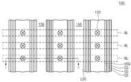
도 1, 도 2a 내지 도 2f, 그리고 도 3을 참조하여, 본 발명의 일 실시예에 따른 반도체 소자의 형성방법이 설명된다. 도 1은 본 발명의 일 실시예에 따른 반도체 소자의 평면도이고, 도 2a 내지 도 2f, 및 도 3은 도 1에 도시된 Ⅰ-Ⅱ을 따라 취한 본 발명의 일 실시예에 따른 반도체 소자의 공정 단면도이다.Referring to Figs. 1, 2A to 2F, and 3, a method of forming a semiconductor device according to an embodiment of the present invention will be described. FIG. 1 is a plan view of a semiconductor device according to an embodiment of the present invention. FIGS. 2A to 2F and 3 are cross-sectional views of a semiconductor device according to an embodiment of the present invention taken along the line I- Sectional view.
도 1 및 도 2a를 참조하면, 반도체 기판(이하, '기판', 100)이 준비된다. 상기 기판(100)은 도펀트들로 도핑된 웰 영역을 포함할 수 있다. 상기 기판(100) 상에 기저 절연막(121)이 형성된다.Referring to FIGS. 1 and 2A, a semiconductor substrate (hereinafter referred to as a "substrate") 100 is prepared. The
상기 기저 절연막(121) 상에 희생막들(SC) 및 게이트간 절연막들(123)이 교대로 적층된다. 상기 게이트간 절연막들(123)은 상기 기저 절연막(121)과 동일한 물질로 형성될 수 있다. 상기 게이트간 절연막들(123)과 상기 희생막들(SC)은 동일한 식각 용액에 대해 서로 다른 식각 선택비를 갖는 물질들을 각각 포함할 수 있다. 예를 들어 상기 게이트간 절연막들(123)이 산화물을 포함하는 경우, 상기 희생막들(SC)은 질화물을 포함할 수 있다. 최상부의 상기 희생막(SC) 상에 상부 절연막(125)이 형성될 수 있다. 상기 상부 절연막(125)은 상기 게이트간 절연막들(123)과 동일한 절연물질을 포함할 수 있다.The sacrificial films SC and the inter-gate
상기 절연막들(121, 123, 125) 및 희생막들(SC)을 이방성 식각하여, 상기 절연막들(121, 123, 125) 및 희생막들(SC)을 관통하는 홀(130)을 형성한다. 상기 홀(130)은 상기 막들을 관통하되, 상기 기판(100) 평면으로부터 수직하게 형성될 수 있다. 이와 달리, 상기 홀(130)을 대신하여 상기 절연막들(121, 123, 125) 및 희생막들(SC)을 관통하되, 상기 기판(100)의 제1 방향을 따라 연장되는 그루브가 형성될 수도 있다.The
상기 홀(130) 내에 반도체 구조물(133)이 형성될 수 있다. 상기 반도체 구조물(133)은 반도체 원소, 예를 들어 주기율표상의 4A족 원소들을 포함할 수 있다. 상기 반도체 구조물(133)은 단결정 또는 다결정 상태의 반도체 원소를 포함할 수 있다. 본 실시예에서, 상기 반도체 구조물(133)은 형성되는 트랜지스터의 채널 영역이 형성되는 활성 패턴일 수 있다.A
상기 반도체 구조물(133)은 상기 홀(130)을 채우는 필라 형태(pillar type) 일 수 있다. 이와 달리, 상기 반도체 구조물(133)은 내부 공간을 포함하는 쉘(shell)형태일 수 있다. 이 경우, 상기 내부 공간은 절연막에 의해 채워질 수 있다. 상기 홀(130) 대신 그루브가 형성된 경우, 상기 그루브를 채우는 반도체 막이 형성되고 상기 반도체막의 형성 직후 또는 이후의 공정에 의해 패터닝되어 상기 필라 형태의 반도체 구조물(133)이 형성될 수도 있다.The
상기 반도체 구조물(133)의 윗 부분에 불순물 영역(135)이 형성될 수 있다. 상기 불순물 영역(135)은 상기 반도체 구조물(133)의 상부 내에 도펀트를 주입하여 형성될 수 있다. 이와 달리, 상기 불순물 영역(135)은 인 시츄(in-situ) 공정을 수행하여 형성될 수 있다.An
도 2b를 참조하면, 상기 절연막들(121, 123, 125) 및 희생막들(SC)을 패터닝하여, 상기 절연막들(121, 123, 125) 및 희생막들(SC)을 관통하는 그루브(140)를 형성한다. 상기 그루브(140)는 상기 기판(100) 평면의 제1 방향으로 연장될 수 있다. 상기 그루브(140)에 의해 상기 기판(100)의 상부면 및 패터닝된 상기 절연막들(121, 123, 125) 및 희생막들(SC)의 측벽들이 노출될 수 있다.Referring to FIG. 2B, the insulating
상기 그루브(140) 및 상기 홀(130)은 기울어진 측벽을 가질 수 있다. 이는 상기 그루브(140) 및 상기 홀(130)을 형성하기 위한 이방성 식각 공정에서 식각되는 막의 총 두께가 두꺼운 것에 기인할 수 있다. 이와 달리, 상기 절연막들(121, 123, 125) 및 희생막들(SC)의 총 두께를 적절히 조절하는 경우, 상기 그루브(14) 및 상기 홀(130)의 측벽들은 상기 기판(100)의 상부면에 대해 실질적으로 수직할 수 있다.The
도 2c를 참조하면, 상기 희생막들(SC)이 제거된다. 상기 희생막들(SC)이 질화물을 포함하는 경우, 상기 희생막들(SC)은 인산(H3PO4) 용액을 식각 용액으로 사용하는 습식 식각 공정에 의해 제거될 수 있다. 상기 희생막들(SC)의 제거에 의해 상기 절연막들(121, 123, 125) 사이에 오프닝들(150)이 형성될 수 있다. 상기 오프닝들(150)에 의해 상기 반도체 구조물(133)의 측벽의 일부가 노출될 수 있다. 또한, 상기 오프닝들(150)에 의해 상기 기저절연막(121)의 상부면, 상기 게이트간 절연막들(123) 및 상기 상부 절연막(125)의 상부면들 및 하부면들이 노출될 수 있다.Referring to FIG. 2C, the sacrificial layers SC are removed. If the sacrificial layers SC include nitride, the sacrificial layers SC may be removed by a wet etching process using a phosphoric acid (H3 PO4 ) solution as an etching solution.
상기 그루브(140) 및 상기 오프닝들(150) 내에 절연패턴(142)이 형성된다. 상기 절연패턴(142)은 상기 그루브(140) 및 상기 오프닝들(150)의 벽들을 콘포말하게 덮을 수 있다. 상기 절연패턴(142)은 상기 오프닝들(150)에 의해 노출된 상기 반도체 구조물(133)의 측벽 상에 형성될 수 있다. 상기 절연패턴(142)은 상기 게이트간 절연막들(123) 및 상부 절연막(125)의 상부면들 및 하부면들과 상기 기저 절연막(121)의 상부면을 덮을 수 있다. 상기 절연패턴(142)은 상기 절연막들(121, 123, 125)의 측벽들 상에도 형성될 수 있다. 상기 절연막들(121, 123, 125)의 상부면 및 하부면들 상의 상기 절연패턴(142)은 상기 오프닝들(150)의 측벽을 정의할 수 있다.An
상기 절연패턴(142)은 복수의 절연막들로 구성될 수 있다. 상기 절연패턴(142)은 전하저장층을 포함할 수 있다. 예를 들어, 상기 절연패턴(142)은 ONO(Oxide-Nitride-Oxide)막 또는 ONOA(Oxide-Nitride-Oxide-AluminiumOxide)막을 포함할 수 있다. 일 실시예에서, 상기 질화막(Nitride)은 상기 전하저장층으로 작용할 수 있다.The insulating
상기 절연패턴(142) 상에 베리어층(144)이 형성될 수 있다. 상기 베리어층(144)은 상기 그루브(140) 및 상기 오프닝들(150)의 바닥들 및 측벽들 상에 콘포말하게 형성될 수 있다. 상기 베리어층(144)은 100Å이하로 형성될 수 있다. 예를 들어, 상기 베리어층(144)은 50Å이하로 형성될 수 있다. 상기 베리어층(144)은 금속 질화물을 포함할 수 있다. 예를 들어, 상기 베리어층(144)은 텅스텐질화물(WN) 또는 티타늄질화물(TiN)을 포함할 수 있다.A
도 2d를 참조하면, 상기 오프닝들(150) 및 상기 개구부(140) 내에 제1 금속막(153)이 형성될 수 있다. 상기 제1 금속막(153)은 상기 개구부(140)의 일부를 채울 수 있다.Referring to FIG. 2D, a
상기 제1 금속막(153)을 형성하는 것은, 상기 오프닝들(150) 및 상기 개구부(140) 내에 제1 금속 소오스 및 제1 환원 가스를 제공하는 것을 포함할 수 있다. 상기 제1 금속 소오스는 제1 금속을 포함할 수 있다. 예를 들어, 상기 제1 금속 소오스는 전이금속을 포함하는 화합물일 수 있다. 상기 제1 환원 가스는 상기 제1 금속 소오스에 포함된 상기 금속을 환원시킬 수 있다. 예를 들어, 상기 제1 환원 가스는 수소가스, 수소 라디칼 또는 수소 이온을 공급할 수 있는 화학종일 수 있다.The forming of the
일 실시예에서, 상기 제1 금속 소오스는 WF6이고, 상기 제1 환원 가스는 실란(SiH4)또는 디보란(B2H6)일 수 있다. 상기 제1 금속 소오스 및 상기 제1 환원 가 스를 도 2c의 결과물을 포함하는 기판(100) 이 로딩된 반응 챔버 내에 제공시, 하기 화학식 1에 해당하는 반응이 일어날 수 있다.In one embodiment, the first metal source is WF6 and the first reducing gas is silane (SiH4 ) Or diborane (B2 H6 ). When the first metal source and the first reducing gas are provided in a reaction chamber loaded with the
2WF6 + 3SiH4 -> 2W + 3SiF4 + 6H2 (화학식 1)2WF6 + 3SiH4 - > 2W + 3SiF4 + 6H2 (Formula 1)
상기 화학식 1에서 육플루오르화텅스텐(WF6)은 제1 금속 소오스에 해당하고, 실란(SiH4)은 상기 제1 환원 가스에 해당한다. 상기 제1 금속 소오스와 상기 제1 환원가스의 반응은 상대적으로 빠른 반응일 수 있다. 이에 따라, 상기 오프닝들(150) 및 상기 개구부(140) 내에 제1 금속막(153)이 빠른 속도로 증착될 수 있다. 빠른 속도로 증착되는 상기 제1 금속막(153)의 그레인의 크기는 상대적으로 작을 수 있다.In Formula 1, tungsten hexafluoride (WF6 ) corresponds to the first metal source, and silane (SiH4 ) corresponds to the first reducing gas. The reaction between the first metal source and the first reducing gas may be a relatively fast reaction. Accordingly, the
도 2e를 참조하면, 상기 제1 금속막(153)의 일부가 식각되어 상기 오프닝들(150) 내에 제1 금속패턴들(154)이 형성된다. 상기 제1 금속막(153)은 습식 식각될 수 있다. 예를 들어, 상기 제1 금속막(153)은 H2O2, H3PO4, HNO3, CH3COOH, HF, HCl, H2SO4, EKC, SF6, Cl2 및 NF3중 적어도 하나를 포함하는 식각 용액에 의해 식각될 수 있다. 상기 제1 금속막(153)이 식각됨으로써, 하나의 오프닝 내에 하나의 제1 금속패턴이 형성될 수 있다. 즉, 상기 습식 식각에 의해 상기 제1 금속막(153)의 노드 분리(node isolation)가 일어날 수 있다.Referring to FIG. 2E, a portion of the
상기 제1 금속막(153)은 습식 식각에 의해 식각되므로, 상기 제1 금속막(153)의 식각 공정에서 발생할 수 있는 식각 부산물이 상기 절연패턴(142)의 표면을 오염시키는 것을 방지할 수 있다. 또한, 상기 제1 금속막(153)은 비교적 작은 그레인 크기를 가지므로 상기 습식 식각에 의한 에칭 손상(etching damage)이 최소화될 수 있다. 상기 습식 식각 이후 세정 공정이 추가로 수행될 수 있다. 상기 습식 식각 공정 및/또는 상기 세정 공정에 의해 상기 절연패턴(142) 상의 댕글링 본딩 등이 제거될 수 있다.Since the
상기 제1 금속막(153)의 식각시, 상기 베리어층(144)이 함께 식각되어 베리어 패턴(145)이 형성될 수 있다. 상기 베리어 패턴(145)의 식각에 의해 상기 오프닝들(150)의 측벽을 정의하는 상기 절연패턴(142)의 일부가 노출될 수 있다. 상기 베리어 패턴(145)의 식각된 면은 상기 제1 금속패턴(154)의 식각된 면과 공면을 이룰 수 있다.When the
상기 제1 금속패턴(154) 및 상기 베리어 패턴(145)의 식각된 면들은 상기 게이트간 절연막들(123)의 측벽들과 접하는 상기 절연패턴(142)의 일 면보다 상기 오프닝들(150)의 안쪽에 위치할 수 있다.The
도 2f를 참조하면, 상기 제1 금속패턴(154)의 식각된 면으로부터 제2 금속패턴(156)이 형성된다. 상기 제2 금속패턴(156)은 상기 제1 금속패턴(154)의 식각된 면으로부터 선택적으로 형성될 수 있다. 하나의 오프닝 내에 형성된 상기 제1 금속패턴(154)과 상기 제2 금속패턴(156)은 하나의 게이트 패턴(LSG, CG, USG)을 구성할 수 있다. 상기 기판(100)에 가장 인접한 게이트 패턴(LSG)은 하부 선택 게이트 패턴이고, 게이트 패턴들(LSG, CG, USG) 중 최상부의 게이트 패턴(USG)은 상부 선택 게이트 패턴일 수 있다. 상기 하부 선택 게이트 패턴(LSG)과 상기 상부 선택 게이트 패턴(USG) 사이의 게이트 패턴들은 메모리 셀 게이트 패턴들(CG)일 수 있다.Referring to FIG. 2F, a
상기 제2 금속패턴(156)을 상기 제1 금속패턴(154)의 식각된 면 상에 선택적으로 형성하는 것은, 제2 금속 소오스를 제공하는 것 및 상기 반응 챔버 내에 제2 환원 가스를 제공하는 것을 포함할 수 있다.Selectively forming the
상기 제2 금속 소오스는 제2 금속을 포함할 수 있다. 일 실시예에서, 상기 제2 금속 소오스는 상기 제1 금속 소오스와 동일한 금속을 포함할 수 있다. 예를 들어, 상기 제2 금속 소오스가 육플루오르화텅스텐(WF6)이고 상기 제2 환원 가스가 수소(H2)가스인 경우, 상기 반응 챔버 내에서 일어나는 반응은 다음의 화학식과 같을 수 있다.The second metal source may comprise a second metal. In one embodiment, the second metal source may comprise the same metal as the first metal source. For example, when the second metal source is tungsten hexafluoride (WF6) and the second reducing gas is hydrogen (H2 ) gas, the reaction occurring in the reaction chamber may be represented by the following chemical formula.
2WF6 + 3H2 -> W + 6HF (화학식 2)2WF6 + 3H2 - > W + 6HF (Formula 2)
상기 화학식 2에 대응하는 화학반응은 상기 제1 금속패턴(154)의 식각된 면 상에서 일어날 수 있다. 상기 제2 금속 소오스 및 제2 환원 가스는 상기 제1 금속패턴(154)의 식각된 면 상에 흡착될 수 있다. 상기 제2 환원 가스는 원자 상태로 분해되고 분해된 원자 상태의 제2 환원 가스가 상기 흡착된 제2 금속 소오스와 반응하여, 상기 제1 금속패턴(154)의 식각된 면 상에 상기 제2 금속이 증착될 수 있 다.The chemical reaction corresponding to Formula 2 may occur on the etched surface of the
상기 제2 금속패턴(156)의 형성을 위한 반응은 상대적으로 느린 반응일 수 있다. 예를 들어, 상기 제2 금속패턴(156)의 형성을 위한 반응은 상기 제1 금속막(153)의 형성을 위한 반응보다 느린 속도로 진행될 수 있다. 상기 제2 금속패턴(156)은 상기 제2 금속패턴(154)보다 큰 그레인 크기를 가질 수 있다.The reaction for forming the
상기 제2 금속패턴(156)의 형성 공정은 저온 및 저압 조건 하에서 수행될 수 있다. 예를 들어, 상기 제2 금속패턴(156)의 형성시 상기 반응 챔버 내의 온도는 500℃이하이고, 상기 반응 챔버 내의 압력은 50Torr이하일 수 있다. 일 실시예에서, 상기 제2 금속패턴(156)시 반응 챔버 내의 온도는 350℃이고, 상기 반응 챔버 내의 압력은 40Torr이하일 수 있다.The process of forming the
금속 원자의 증착의 개시를 위해, 금속 소오스가 증착 대상막에 제공되고 상기 금속 소오스가 상기 증착 대상막으로부터 전자를 받아들인다(accept). 상기 금속 소오스가 전자를 받아들이는 것에 의해, 상기 금속 소오스의 금속에 붙어있던 다른 원자들의 적어도 일부가 상기 금속 소오스로부터 분리될 수 있다. 예를 들어, WF6가 금속 소오스로 사용되는 경우, 상기 증착 대상막에서 제공된 전자에 의해 상기 WF6는 WFn와 F6-n(n은 6이하의 정수)으로 분리될 수 있다. 분리된 플루오르 원자(F)는 상기 식각대상막을 구성하는 일 원자와 상기 제공된 전자를 공유함으로써 결합될 수 있다. 상기 결합된 일 원자와 플루오르 원자는 기체 상태로 상기 증착 대상막으로부터 제거됨으로써, 상기 증착 대상막 상에 상기 금속이 증착되게 된다.To initiate the deposition of the metal atoms, a metal source is provided to the deposition target film and the metal source accepts electrons from the deposition target film. The metal source accepts electrons so that at least a part of other atoms attached to the metal of the metal source can be separated from the metal source. For example, when WF6 is used as a metal source, the WF6 can be separated into WFn and F6-n (n is an integer of 6 or less) by electrons provided in the deposition target film. The separated fluorine atoms (F) may be bonded by sharing the provided electrons with the atoms constituting the etching target film. The bonded atoms and the fluorine atoms are removed from the deposition target film in a gaseous state, so that the metal is deposited on the deposition target film.
상술한 금속 원자의 증착 과정에서 상기 금속 원자가 상기 증착 대상막에 증착되는 일 요인은, 상기 증착 대상막으로부터의 상기 금속 소오스로의 전자의 제공일 수 있다. 따라서, 상기 증착 대상막이 쉽게 전자를 제공할수록 상기 금속 원자의 증착은 원활하게 진행될 수 있다. 상기 증착 대상막이 전자를 제공하는 정도는 상기 증착 대상막을 구성하는 화합물의 결합의 종류에 의해 영향을 받을 수 있다. 증착 대상막을 구성하는 화합물들은 금속결합, 공유결합 또는 이온결합을 포함하는 결합들에 의해 결합될 수 있다. 상기 화합물들은 복수의 결합 요인들에 의해 결합될 수 있으나 상기 복수의 결합들 중 어느 하나가 우세할 수 있다. 예를 들어, 금속 원자들 사이의 결합에서는 다른 결합들보다 금속결합이 우세하고, 비금속원자들 사이의 결합에서는 다른 결합들보다 공유결합이 우세할 수 있다. 본 명세서의 상세한 설명 및 특허청구범위에서는, 설명의 편의상 원자들 사이의 결합 중 가장 우세한 결합에 의해 상기 원자들이 결합된 것으로 설명된다. 상기 증착 대상막을 구성하고 있는 화합물이 이온 결합에 의해 결합된 화합물인 경우 상기 증착 대상막은 상대적으로 상기 금속 소오스에 적은 양의 전자를 제공할 수 있다. 특히, 상기 증착 대상막을 구성하고 있는 화합물이 강한 이온 결합을 하고 있는 경우, 상기 증착 대상막은 상기 금속 소오스에 전자를 쉽게 제공하지 않을 수 있다. 이와 달리, 상기 증착 대상막을 구성하고 있는 화합물이 금속 결합에 의해 결합된 화합물인 경우 상기 증착 대상막은 상대적으로 상기 금속 소오스에 많은 양의 전자를 제공할 수 있다. 따라서, 상기 증착 대상막에 금속 소오스를 제공함으로써 금속층을 형성하는 경우 상기 증착막을 구성하는 결합의 종류에 의해 금속층의 형성이 제어될 수 있 다.One factor that the metal atoms are deposited on the deposition target film during the deposition of the metal atoms may be the provision of electrons from the deposition target film to the metal source. Therefore, as the deposition target film easily provides electrons, the deposition of the metal atoms can proceed smoothly. The degree to which the deposition target film provides electrons may be influenced by the kind of binding of the compound constituting the deposition target film. The compounds constituting the film to be deposited may be bonded by bonds including a metal bond, a covalent bond or an ionic bond. The compounds may be bound by a plurality of binding factors, but any one of the plurality of bonds may predominate. For example, a bond between metal atoms dominates a metal bond over other bonds, and a bond between nonmetal atoms may dominate a covalent bond over other bonds. In the description and claims of this specification, for convenience of explanation, the atoms are described as being bonded by the most predominant bond among the bonds between atoms. When the compound constituting the deposition target film is a compound bonded by ionic bonding, the deposition target film can relatively provide a small amount of electrons to the metal source. Particularly, when the compound constituting the deposition target film is strongly ion-bonded, the deposition target film may not easily provide electrons to the metal source. Alternatively, when the compound constituting the deposition target film is a compound bonded by metal bonding, the deposition target film may relatively provide a large amount of electrons to the metal source. Therefore, when a metal layer is formed by providing a metal source to the deposition target film, the formation of the metal layer can be controlled by the kind of the bond constituting the deposition film.
따라서, 상기 제2 금속패턴의 형성을 위한 금속 원자의 증착은 선택적으로 이루어질 수 있다. 상기 절연패턴(142)을 구성하는 화합물은 강한 이온결합에 의해 결합된 화합물일 수 있다. 예를 들어, 상기 오프닝들(150)에 의해 노출되는 상기 절연패턴(142)의 표면은 산화물을 포함할 수 있다. 강한 이온결합을 포함하는 상기 화합물은 상기 제2 금속 소오스에 전자를 덜 제공할 수 있다. 따라서, 상기 제2 금속 소오스 및 상기 제2 환원 가스가 상기 절연패턴(142) 상에 쉽게 흡착되지 않을 수 있다. 구체적으로, 상기 제2 금속막(156)의 증착을 위한 반응은, 상기 제2 금속 소오스 및 상기 제2 환원 가스의 흡착을 포함할 수 있다. 따라서, 상기 제2 금속 소오스 및 상기 제2 환원 가스가 상기 절연패턴(142) 상에 쉽게 흡착되지 않으므로, 상기 절연패턴(142) 상에 상기 제2 금속패턴(156)이 쉽게 형성되지 않을 수 있다.Thus, deposition of the metal atoms for formation of the second metal pattern may be selectively performed. The compound constituting the insulating
이에 반해, 상기 제1 금속패턴(154)은 금속 결합에 의해 구성된 화합물들을 포함하므로 상기 제1 금속패턴(154)은 상기 제2 금속 소오스에 상대적으로 많은 전자들을 제공할 수 있다. 따라서, 상기 제1 금속패턴(154) 상에 상기 제1 금속 소오스 및 상기 제1 환원 가스가 흡착될 수 있다. 이에 의해 상기 제1 금속패턴(154) 상에 제2 금속들이 용이하게 증착될 수 있다. 상기 금속들의 증착되는 정도의 차이에 의해, 상기 제1 금속패턴(154) 상에 선택적으로 제2 금속패턴(156)이 형성될 수 있다.In contrast, since the
상기 제2 금속패턴(156)은 선택성장하므로, 인접한 오프닝들(150) 내의 제2 금속패턴(156)을 분리하기 위한 노드 분리 공정은 생략될 수 있다. 이에 따라, 상기 제2 금속패턴(156)의 노드 분리 공정에 의해 발생할 수 있는 상기 제2 금속패턴(156)의 결함이 더욱 감소된다. 구체적으로, 상기 제2 금속패턴(156)은 상기 제1 금속패턴(154)에 비해 상대적으로 큰 그레인 크기를 갖는다. 이에 따라, 상기 제2 금속패턴(156)의 노드 분리 공정시 상기 제2 금속패턴(156)의 상당 부분이 뜯겨질 수 있다. 이는 상기 제2 금속패턴(156)의 저항 특성에 악영향을 미친다. 그러나, 본 발명의 실시예들에 따르면 상기 노드 분리 공정이 생략될 수 있어 상기 노드 분리 공정시 발생할 수 있는 상기 제2 금속패턴(156)의 결함이 최소화된다. 또한, 인접한 오프닝들(150) 내에서 서로 전기적으로 분리된 상태로 상기 제2 금속패턴(156)이 형성되므로 인접한 게이트 패턴들이 보다 완전히 절연될 수 있다.Since the
상기 제2 금속패턴(156)은 도 4a에 도시된 바와 같이, 상기 게이트간 절연막들(123)의 측벽들 상의 상기 절연패턴(142)의 측벽까지 성장될 수 있다. 이와 달리, 상기 제2 금속패턴(156)은 도 4b에 도시된 바와 같이 상기 게이트간 절연막들(123)의 측벽들 상의 상기 절연패턴(142)의 측벽보다 돌출될 수 있다. 즉, 상기 제2 금속패턴(156)은 과성장(overgrowth)될 수 있다. 이에 의해 상기 제2 금속패턴(156)을 포함하는 게이트 패턴의 저항이 감소될 수 있다. 상기 제2 금속패턴(156)의 성장 정도를 제어하여 형성되는 상기 게이트 패턴의 저항이 조절될 수 있다.The
본 발명의 실시예들에 따른 제1 금속패턴(154) 및 제2 금속패턴(156)의 형성방법은 패턴 형성과정에서 발생할 수 있는 물리적 결함들, 예를 들어, 보이드 및 심을 감소시킬 수 있다. 앞서 설명한 바와 같이 상기 제1 금속패턴(154)은 습식 식각에 의해 식각되므로, 상기 제1 금속패턴(154)의 식각 부산물, 예를 들어, 제1 금속 소오스에 포함된 금속 원자들이 상기 절연패턴(142)을 오염시키는 것이 최소화된다. 이에 따라, 상기 절연패턴(142) 상에 상기 식각 부산물이 부착되고 상기 부착된 식각 부산물로부터 제2 금속패턴(154)이 성장되는 것이 방지될 수 있다. 상기 식각 부산물을 핵으로 성장하는 제2 금속은 상기 제1 금속패턴(154)으로부터 성장되는 제2 금속과 다른 방향으로부터 성장되므로 이에 의해 형성되는 제2 금속패턴(154)은 상기 물리적 결함을 갖게 된다. 또한, 상기 식각 부산물은 상기 절연패턴(142) 상에 불규칙적으로 형성되므로, 상기 식각 부산물로부터 성장되는 상기 제2 금속패턴(154)을 제어하는 것이 어려울 수 있다. 그러나, 본 발명의 실시예들에 따라, 상기 제1 금속패턴(154)으로부터 선택적으로 제2 금속패턴(156)이 형성되는 경우, 상기 물리적 결함이 최소화된 제2 금속패턴(156)이 형성될 수 있다. 이에 따라, 상기 제2 금속패턴(156)을 포함하는 반도체 소자의 신뢰성이 향상될 수 있다.The method of forming the
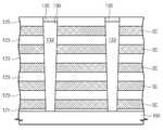
도 3을 참조하면, 상기 개구부(140)를 채우는 충진 절연막(158)이 형성된다. 상기 충진 절연막(158)에 의해, 일 반도체 구조물(133)을 공유하며 적층된 제1 및 제2 금속패턴들(154, 156)과 인접한 다른 반도체 구조물(133)을 공유하며 적층된 제1 및 제2 금속패턴들(154, 156)이 분리된다. 상기 충진 절연막(158)의 상부면은 평탄화될 수 있다. 상기 평탄화시, 상기 상부 절연막(125) 및 상기 반도체 구조물(133) 상의 상기 절연패턴(142)이 함께 제거될 수 있다. 상기 평탄화는 상부 절연막(125)의 상부면 및 상기 반도체 구조물(133) 내의 상기 불순물 영역(135)의 상부면이 노출될 때까지 수행될 수 있다.Referring to FIG. 3, a filling insulating
상기 반도체 구조물(133) 및 상기 상부 절연막(125) 상에 층간 절연막(161)이 형성된다. 상기 층간 절연막(161)을 관통하는 비트라인 콘택홀을 형성한다. 상기 비트라인 콘택홀은 상기 불순물 영역(135)의 상부면을 노출시킬 수 있다. 상기 비트라인 콘택홀을 채우는 비트라인 콘택(163)이 형성된다. 상기 비트라인 콘택(163)은 금속, 도핑된 반도체 또는 금속 화합물을 포함할 수 있다. 상기 층간 절연막(161) 및 상기 비트라인 콘택(163) 상에 비트라인(165)이 형성된다. 상기 비트라인(165)은 상기 제1 방향과 교차하는 제2 방향을 따라 연장될 수 있다. 상기 비트라인 콘택(163) 및 상기 비트라인(165)은 동시에 또는 별도로 형성될 수 있다.An interlayer insulating
도 1, 도 3, 도 4a 및 도 4b를 참조하여, 본 발명의 일 실시예에 따른 반도체 소자가 설명된다. 앞서 도 1, 도 2a 내지 도 2f, 도 3, 도 4a 및 도 4b를 참조하여 설명된 내용은 생략될 수 있다.1, 3, 4A and 4B, a semiconductor device according to an embodiment of the present invention will be described. The contents described above with reference to FIG. 1, FIG. 2A to FIG. 2F, FIG. 3, FIG. 4A and FIG. 4B may be omitted.
도 1 및 도 3을 참조하면, 기판(100) 상에 반도체 구조물(133)이 배치된다. 상기 반도체 구조물(133)은 상기 기판(100)으로부터 위로 연장되는 기둥형태일 수 있다. 상기 반도체 구조물(133)은 단결정 또는 다결정 반도체 물질을 포함할 수 있다. 상기 반도체 구조물(133)의 최상부 내에 불순물 영역(135)이 제공될 수 있다. 상기 불순물 영역(135)은 상기 반도체 구조물(133)의 다른 부분보다 높은 도펀트 농도를 갖는 부분일 수 있다.Referring to FIGS. 1 and 3, a
상기 반도체 구조물(133)의 측벽을 따라 절연막들(121, 123, 125)이 적층될 수 있다. 상기 절연막들(121, 123, 125)은 상기 기판(100)에 가장 인접한 기저 절연막(121), 상기 기저 절연막(121) 상의 복수의 게이트간 절연막들(123), 그리고 최상부 게이트간 절연막(123) 상의 상부 절연막(125)을 포함할 수 있다. 상기 절연막들(121, 123, 125)은 서로 이격되어 상기 반도체 구조물(133)의 측벽 상에 배치될 수 있다.Insulating
상기 반도체 구조물(133)의 측벽 및 상기 절연막들(121, 123, 125)을 덮는 절연패턴(142)이 제공된다. 상기 절연패턴(142)은 상기 절연막들(121, 123, 125) 사이의 상기 반도체 구조물(133)의 측벽, 상기 절연막들(121, 123, 125)의 상부면들, 하부면들 및 측벽들을 덮을 수 있다. 상기 절연패턴(142)은 복수의 층들을 포함할 수 있다. 상기 절연패턴(142)은 산화막, 질화막 또는 이들의 조합을 포함할 수 있다. 예를 들어, 상기 절연패턴(142)은 ONO막 또는 ONOA막일 수 있다.An
인접한 상기 절연막들(121, 123, 125) 사이에 오프닝들(150)이 정의될 수 있다. 상기 오프닝들(150)은 상기 인접한 절연막들(121, 123, 125) 사이의 상기 절연패턴(142)에 의해 한정된 공간일 수 있다. 상기 오프닝들(150)은 상기 반도체 구조물(133)의 측벽 상의 상기 절연패턴(142)에 의해 정의되는 바닥들과 상기 절연막들(121, 123, 125)의 상부면들과 하부면들에 상의 상기 절연패턴(142)에 정의되는 측벽들을 포함한다.
상기 오프닝들(150)은 게이트 패턴으로 채워질 수 있다. 상기 게이트 패턴은 상기 오프닝들(150)의 바닥에 인접한 제1 금속패턴(154)과 상기 제1 금속패턴(154)의 측벽 상의 제2 금속패턴(156)을 포함할 수 있다.The
도 4a를 참조하면, 상기 제2 금속패턴(156)의 일 측벽은 상기 반도체 구조물(133)과 인접하지 않는 상기 절연막들(121, 123, 125)의 측벽들 상의 상기 절연패턴(142)의 측벽과 공면을 이룰 수 있다. 이와 달리, 상기 제2 금속패턴(156)의 일 측벽은, 도 4b에 도시된 바와 같이 상기 절연막들(121, 123, 125)의 측벽들 상의 상기 절연패턴(142)의 측벽보다 옆으로 돌출될 수 있다. 이와 달리, 상기 제2 금속패턴(156)의 일 측벽은 상기 오프닝들(150) 내에 배치될 수도 있다. 예를 들어, 상기 제2 금속패턴(156)은 상기 절연막들(121, 123, 125)의 측벽들보다 함몰될 수 있다. 상기 제2 금속패턴(156)의 형태는 적용되는 소자에 따라 적절히 선택될 수 있다.4A, one side wall of the
상기 제1 금속패턴(154)과 상기 제2 금속패턴(156)은 동일한 금속을 포함할 수 있다. 예를 들어, 상기 제1 금속패턴(154) 및 상기 제2 금속패턴(156)은 텅스텐을 포함할 수 있다. 상기 제1 금속패턴(154)의 그레인의 크기와 상기 제2 금속패턴(156)의 그레인의 크기는 서로 다를 수 있다. 예를 들어, 상기 제1 금속패턴(154)의 그레인의 크기는 상기 제2 금속 패턴(156)의 그레인의 크기보다 작을 수 있다. 이에 의해, 상기 제1 금속패턴(154)의 비저항은 상기 제2 금속패턴(156)의 비저항보다 클 수 있다.The
상기 제1 금속패턴(154)의 상부면 및 하부면 상에 베리어패턴(145)이 제공될 수 있다. 상기 베리어패턴(145)은 상기 제1 금속패턴(154)과 상기 반도체 구조물(133) 사이로 연장될 수 있다. 상기 베리어패턴(145)은 질화티타늄(TiN) 및 질화텅스텐(WN)을 포함하는 금속화합물 중 선택된 적어도 하나를 포함할 수 있다.A
상기 기판(100) 상에 상기 반도체 구조물(133), 상기 게이트 패턴들, 상기 절연막들(121, 123, 125) 및 상기 절연패턴들로 구성된 일 적층구조 및, 상기 일 적층구조와 실질적으로 동일한 다른 적층구조가 배치될 수 있다. 상기 적층구조들 사이는 충진 절연막(158)이 배치될 수 있다. 상기 충진 절연막(158)은 상기 절연막들(121, 123, 125)의 측벽들 상의 상기 절연패턴(142)과 상기 제2 금속패턴(156)의 일 측벽과 접할 수 있다.A laminated structure consisting of the
상기 충진 절연막(158), 상기 상부 절연막(125) 및 상기 반도체 구조물(133) 상에 비트라인(165)이 제공된다. 상기 비트라인(165)은 상기 반도체 구조물(133)과 비트라인 콘택(163)에 의해 연결될 수 있다. 상기 비트라인(165)과 상기 상부 절연막(125) 및 상기 충진 절연막(158) 사이에는 층간 절연막(161)이 더 배치될 수 있다.A
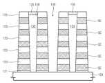
도 5a 내지 도 5c를 참조하여, 본 발명의 다른 실시예에 따른 반도체 소자의 형성방법이 설명된다.5A to 5C, a method of forming a semiconductor device according to another embodiment of the present invention will be described.
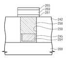
도 5a를 참조하면, 반도체 구조물(200)이 준비된다. 상기 반도체 구조물(200)은 반도체 기판일 수 있다. 상기 반도체 구조물(200)은 도전 영역 및/또는 절연 영역을 포함할 수 있다. 상기 반도체 구조물(200) 상에 오프닝(250)을 정의하는 절연패턴(242)이 형성된다. 상기 절연패턴(242)은 이온 결합에 의해 결합되는 원자들을 포함할 수 있다. 상기 절연패턴(242)은 예를 들어, 산화물을 포함할 수 있다. 상기 오프닝(250)은 상기 반도체 구조물(200)의 상부면을 노출시킬 수 있다. 예를 들어, 상기 오프닝(250)은 상기 반도체 구조물(200)의 도전 영역의 상부면을 노출시킬 수 있다. 상기 오프닝(250)은 상기 반도체 구조물(200)의 상부면에 의해 정의되는 바닥과 상기 절연패턴(242)의 측벽에 의해 정의되는 측벽을 포함할 수 있다.Referring to FIG. 5A, a
상기 오프닝(250) 내에 베리어층(244)이 형성될 수 있다. 상기 베리어층(244)은 상기 노출된 반도체 구조물(200)의 상부면(상기 오프닝(250)의 바닥), 상기 오프닝(250)의 측벽 및 상기 절연패턴(242)의 상부면 상에 콘포말하게 형성될 수 있다. 상기 베리어층(244)은 금속화합물을 포함할 수 있다. 예를 들어, 상기 베리어층(244)은 티타늄질화물 또는 텅스텐질화물을 포함할 수 있다.A
상기 오프닝(250)을 채우는 제1 금속막(253)이 형성될 수 있다. 상기 제1 금속막(253)을 형성하는 것은, 제1 금속 소오스를 제공하는 것 및 상기 반응 챔버 내에 제1 환원 가스를 제공하는 것을 포함할 수 있다. 상기 제1 금속 소오스는 제1 금속을 포함할 수 있다. 상기 환원 가스는 수소 원자, 수소 라디칼 또는 수소 이온을 포함할 수 있다. 상기 제1 금속 소오스와 상기 제1 환원 가스는 비교적 빠른 반응을 하는 물질들을 포함할 수 있다. 예를 들어, 상기 제1 금속 소오스는 육플루오르화텅스텐(WF6)이고, 상기 제1 환원 가스는 실란(SiH4) 또는 디보란(B2H6)일 수 있다. 이후, 상기 제1 금속 소오스가 육플루오르화텅스텐이 제1 금속 소오스로 사용되고, 실란(silane)이 제1 환원 가스로 사용되는 실시예가 설명된다. 상기 제1 금속 소오스와 상기 제1 환원 가스 사이의 반응은 하기의 (화학식 1)과 같은 반응식 으로 표현될 수 있다.A
2WF6 + 3SiH4 -> 2W + 3SiF4 + 6H2 (화학식 1)2WF6 + 3SiH4 - > 2W + 3SiF4 + 6H2 (Formula 1)
상기 화학식에서 육플루오르화텅스텐(WF6)은 제1 금속 소오스에 해당하고, 실란(SiH4)은 상기 제1 환원 가스에 해당한다. 상기 제1 금속 소오스와 상기 제1 환원가스의 반응은 상대적으로 빠른 반응일 수 있다. 이에 따라, 제1 금속막(253)이 빠른 속도로 증착될 수 있다. 이와 같이 빠른 속도로 증착되는 상기 제1 금속막(253)의 그레인의 크기는 상대적으로 작을 수 있다.In the above formula, tungsten hexafluoride (WF6 ) corresponds to the first metal source, and silane (SiH4 ) corresponds to the first reducing gas. The reaction between the first metal source and the first reducing gas may be a relatively fast reaction. Accordingly, the
도 5b를 참조하면, 상기 제1 금속막(253) 및 상기 베리어층(244)이 습식 식각될 수 있다. 상기 제1 금속막(253) 및 상기 베리어층(244)은 H2O2, H3PO4, HNO3, CH3COOH, HF, HCl, H2SO4, EKC, SF6, Cl2 및 NF3중 적어도 하나를 포함하는 식각 용액에 의해 식각될 수 있다. 상기 습식 식각에 의해 제1 금속패턴(254) 및 베리어패턴(245)이 형성될 수 있다. 상기 제1 금속패턴(254) 및 상기 베리어패턴(245)은 상기 절연패턴(242)의 상부면보다 낮은 상부면을 가질 수 있다. 상기 습식 식각에 의해 상기 오프닝(250)의 측벽의 일부가 노출될 수 있다. 즉, 상기 절연패턴(242)의 측벽의 일부가 노출될 수 있다.Referring to FIG. 5B, the
도 5c를 참조하면, 상기 제1 금속패턴(254) 상에 제2 금속패턴(256)이 선택 적으로 형성된다. 상기 제2 금속패턴(256)은 상기 제1 금속패턴(254) 상에서 이방성 성장할 수 있다.Referring to FIG. 5C, a
상기 제2 금속패턴(256)을 상기 제1 금속패턴(254)의 식각된 면 상에 선택적으로 형성하는 것은, 상기 반응 챔버 내에 제2 금속 소오스를 제공하는 것 및 상기 반응 챔버 내에 제2 환원 가스를 제공하는 것을 포함할 수 있다.Selectively forming the second metal pattern (256) on the etched surface of the first metal pattern (254) comprises providing a second metal source in the reaction chamber and providing a second reducing gas / RTI >
일 실시예에서, 상기 제2 금속 소오스는 상기 제1 금속 소오스와 동일한 금속을 포함할 수 있다. 상기 제2 금속 소오스가 육플루오르화텅스텐(WF6)이고 상기 제2 환원 가스가 수소(H2)가스인 경우, 상기 반응 챔버 내에서 일어나는 반응은 다음의 화학식과 같을 수 있다.In one embodiment, the second metal source may comprise the same metal as the first metal source. When the second metal source is tungsten hexafluoride (WF6 ) and the second reducing gas is hydrogen (H2 ) gas, the reaction occurring in the reaction chamber may be represented by the following chemical formula.
2WF6 + 3H2 -> W + 6HF (화학식 2)2WF6 + 3H2 - > W + 6HF (Formula 2)
상기 화학식 2에 대응하는 화학반응은 상기 제1 금속패턴(254)의 식각된 면 상에서 일어날 수 있다. 상기 제2 금속 소오스 및 제2 환원 가스는 상기 제1 금속패턴(254)의 식각된 면 상에 흡착될 수 있다. 상기 제2 환원 가스는 원자 상태로 분해되고 분해된 원자 상태의 제2 환원 가스가 상기 제2 금속 소오스와 반응하여, 상기 제1 금속패턴(254)의 식각된 면 상에 상기 제2 금속이 증착될 수 있다.The chemical reaction corresponding to Formula 2 may occur on the etched surface of the
상기 제2 금속패턴(256)의 형성을 위한 반응은 상대적으로 느린 반응일 수 있다. 예를 들어, 상기 제2 금속패턴(256)의 형성을 위한 반응은 상기 제1 금속 막(252)의 형성을 위한 반응보다 느린 속도로 진행될 수 있다.The reaction for forming the
일 실시예에서, 상기 제2 금속 소오스와 상기 제2 환원 가스의 반응속도를 늦추기 위해 상기 제2 금속 소오스는 상기 환원 가스보다 많은 양이 제공될 수 있다. 상기 제2 금속패턴(256)의 형성 공정은 저온 및 저압 조건 하에서 수행될 수 있다. 예를 들어, 상기 제2 금속패턴(256)의 형성시 상기 반응 챔버 내의 온도는 500℃이하이고, 상기 반응 챔버 내의 압력은 50Torr이하일 수 있다. 일 실시예에서, 상기 제2 금속패턴(256)시 반응 챔버 내의 온도는 350℃이고, 상기 반응 챔버 내의 압력은 40Torr이하일 수 있다.In one embodiment, the second metal source may be provided in an amount greater than the reducing gas to slow down the reaction rate of the second metal source and the second reducing gas. The process of forming the
도 5c를 재차 참조하여 본 발명의 다른 실시예에 따른 반도체 소자가 설명된다. 앞서, 도 5a 내지 도 5c를 참조하여 설명된 내용은 일부 생략될 수 있다.Referring again to FIG. 5C, a semiconductor device according to another embodiment of the present invention will be described. The contents described above with reference to Figs. 5A to 5C may be partially omitted.
반도체 구조물(200) 상에 절연패턴(242)이 배치된다. 상기 반도체 구조물(200)은 도전 영역 및 절연 영역을 포함하는 반도체 기판일 수 있다. 상기 절연패턴(242)은 상기 반도체 구조물(200)의 도전 영역의 적어도 일부를 노출시키는 오프닝(250)을 정의할 수 있다.An
상기 개구부(250) 내에 제1 금속패턴(254) 및 제2 금속패턴(256)이 배치될 수 있다. 상기 제1 금속패턴(254)은 상기 반도체 구조물(200)에 인접한 상기 오프닝들(150)의 하부에 배치되고, 상기 제2 금속패턴(256)은 상기 제1 금속패턴(254) 상의 상기 오프닝들(150)의 상부에 배치될 수 있다.A
상기 제1 금속패턴(254) 및 상기 제2 금속패턴(256)은 동일한 금속 원소를 포함할 수 있다. 예를 들어, 상기 제1 금속패턴(254) 및 상기 제2 금속패턴(256)은 텅스텐을 포함할 수 있다. 상기 제1 금속패턴(254)과 상기 제2 금속패턴(256)은 서로 상이한 그레인 크기들을 포함할 수 있다. 예를 들어, 상기 제1 금속패턴(254)의 그레인의 크기는 상기 제2 금속패턴(256)의 그레인의 크기보다 작을 수 있다. 이에 따라, 상기 제1 금속패턴(254)의 비저항은 상기 제2 금속패턴(256) 보다 클 수 있다.The
상기 제1 금속패턴(254)과 상기 절연패턴(242) 사이에 베리어패턴(245)이 개재될 수 있다. 상기 베리어패턴(245)의 상부면은 상기 제1 금속패턴(254)의 상부면과 공면을 이룰 수 있다.A
도 6 및 도 7을 참조하여, 본 발명의 다른 실시예들에 의한 반도체 소자의 적용예들이 설명된다.6 and 7, application examples of semiconductor devices according to other embodiments of the present invention are described.
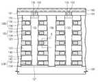
도 6을 참조하면, 도 5c의 제2 금속패턴(256) 상에 가변저항층(263)이 배치된다. 상기 가변저항층(263)은 상변화 물질, 전이금속 산화물 또는 복수의 자성층들을 포함할 수 있다. 이 경우, 상기 제1 금속패턴(254) 및 제2 금속패턴(256)은 콘택 플러그로 작용할 수 있다.Referring to FIG. 6, a
상기 가변저항층(263)의 상부 및 하부에는 상부 전극과 하부 전극이 각각 배치될 수 있다. 상기 하부 전극은 상기 가변저항층(263)과 상기 제2 금속패턴(256) 사이에 개재될 수 있다. 상기 하부 전극은 상기 가변저항층(263)의 특성에 따라 생략될 수 있다.The upper electrode and the lower electrode may be disposed on the upper and lower sides of the
도 7을 참조하면, 도 5c의 제1 금속패턴(254), 제2 금속패턴(256) 및 베리어패턴(245)은 트랜지스터를 구성하는 게이트(212) 및 불순물 영역(203)의 상부와 전기적으로 접속할 수 있다. 이 경우, 상기 제1 금속패턴(254) 및 제2 금속패턴(256)은 콘택 플러그로 작용할 수 있다. 상기 베리어 패턴(245)과 상기 불순물 영역(203) 사이 및/또는 상기 베리어 패턴(245)과 상기 게이트(212) 사이에는 오믹층(216)이 더 개재될 수 있다.Referring to FIG. 7, the
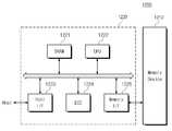
도 8를 참조하면, 본 발명의 실시예에 따른 전자 시스템(1100)은 컨트롤러(1110), 입출력 장치(1120, I/O), 기억 장치(1130, memory device), 인터페이스(1140) 및 버스(1150, bus)를 포함할 수 있다. 상기 컨트롤러(1110), 입출력 장치(1120), 기억 장치(1130) 및/또는 인터페이스(1140)는 상기 버스(1150)를 통하여 서로 결합 될 수 있다. 상기 버스(1150)는 데이터들이 이동되는 통로(path)에 해당한다.8, an
상기 컨트롤러(1110)는 마이크로프로세서, 디지털 신호 프로세스, 마이크로컨트롤러, 및 이들과 유사한 기능을 수행할 수 있는 논리 소자들 중에서 적어도 하나를 포함할 수 있다. 상기 입출력 장치(1120)는 키패드(keypad), 키보드 및 디스플레이 장치등을 포함할 수 있다. 상기 기억 장치(1130)는 데이터 및/또는 명령어등을 저장할 수 있다. 상기 기억 장치(1130)는 상술된 제1 및 제2 실시예들에 개시된 반도체 기억 소자들 중에서 적어도 하나를 포함할 수 있다. 또한, 상기 기억 장치(1130)는 다른 형태의 반도체 기억 소자(ex, 플래쉬 기억 소자, 디램 소자 및/또는 에스램 소자등)를 더 포함할 수 있다. 상기 인터페이스(1140)는 통신 네트워크 로 데이터를 전송하거나 통신 네트워크로부터 데이터를 수신하는 기능을 수행할 수 있다. 상기 인터페이스(1140)는 유선 또는 무선 형태일 수 있다. 예컨대, 상기 인터페이스(1140)는 안테나 또는 유무선 트랜시버등을 포함할 수 있다. 도시하지 않았지만, 상기 전자 시스템(1100)은 상기 컨트롤러(1110)의 동작을 향상시키기 위한 동작 메모리로서, 고속의 디램 및/또는 에스램등을 더 포함할 수도 있다.The
상기 전자 시스템(1100)은 개인 휴대용 정보 단말기(PDA, personal digital assistant) 포터블 컴퓨터(portable computer), 웹 타블렛(web tablet), 무선 전화기(wireless phone), 모바일 폰(mobile phone), 디지털 뮤직 플레이어(digital music player), 메모리 카드(memory card), 또는 정보를 무선환경에서 송신 및/또는 수신할 수 있는 모든 전자 제품에 적용될 수 있다.The
도 9는 본 발명의 일 실시예에 따른 반도체 기억 소자를 포함하는 메모리 카드를 나타내는 블록도이다.9 is a block diagram showing a memory card including a semiconductor memory element according to an embodiment of the present invention.
도 9를 참조하면, 본 발명의 일 실시예에 따른 메모리 카드(1200)는 기억 장치(1210)를 포함한다. 상기 기억 장치(1210)는 상술된 제1 및 제2 실시예들에 개시된 반도체 기억 소자들 중에서 적어도 하나를 포함할 수 있다. 또한, 상기 기억 장치(1210)는 다른 형태의 반도체 기억 소자(ex, 플래쉬 기억 소자, 디램 소자 및/또는 에스램 소자등)를 더 포함할 수 있다. 상기 메모리 카드(1200)는 호스트(Host)와 상기 기억 장치(1210) 간의 데이터 교환을 제어하는 메모리 컨트롤러(1220)를 포함할 수 있다.Referring to FIG. 9, a
상기 메모리 컨트롤러(1220)는 메모리 카드의 전반적인 동작을 제어하는 플 로세싱 유닛(1222)을 포함할 수 있다. 또한, 상기 메모리 컨트롤러(1220)는 상기 프로세싱 유닛(1222)의 동작 메모리로써 사용되는 에스램(1221, SRAM)을 포함할 수 있다. 이에 더하여, 상기 메모리 컨트롤러(1220)는 호스트 인터페이스(1223), 메모리 인터페이스(1225)를 더 포함할 수 있다. 상기 호스트 인터페이스(1223)는 메모리 카드(1200)와 호스트(Host)간의 데이터 교환 프로토콜을 구비할 수 있다. 상기 메모리 인터페이스(1225)는 상기 메모리 컨트롤러(1220)와 상기 기억 장치(1210)를 접속시킬 수 있다. 더 나아가서, 상기 메모리 컨트롤러(1220)는 에러 정정 블록(1224, Ecc)를 더 포함할 수 있다. 상기 에러 정정 블록(1224)은 상기 기억 장치(1210)로부터 독출된 데이터의 에러를 검출 및 정정할 수 있다. 도시하지 않았지만, 상기 메모리 카드(1200)는 호스트(Host)와의 인터페이싱을 위한 코드 데이터를 저장하는 롬 장치(ROM device)를 더 포함할 수도 있다. 상기 메모리 카드(1200)는 휴대용 데이터 저장 카드로 사용될 수 있다. 이와는 달리, 상기 메모리 카드(1200)는 컴퓨터시스템의 하드디스크를 대체할 수 있는 고상 디스트(SSD, Solid State Disk)로도 구현될 수 있다.The
도 1은 본 발명의 일 실시예에 따른 반도체 소자의 평면도이고,1 is a plan view of a semiconductor device according to an embodiment of the present invention,
도 2a 내지 도 2f는 도 1에 도시된 Ⅰ-Ⅱ을 따라 취한 본 발명의 일 실시예에 따른 반도체 소자의 형성 방법을 설명하기 위한 공정 단면도들이고,FIGS. 2A to 2F are cross-sectional views illustrating a method of forming a semiconductor device according to an embodiment of the present invention taken along the line I-II shown in FIG. 1,
도 3은 본 발명의 도 1에 도시된 Ⅰ-Ⅱ을 따라 취한 본 발명의 일 실시예에 따른 반도체 소자의 단면도이고,3 is a cross-sectional view of a semiconductor device according to an embodiment of the present invention taken along the line I-II shown in FIG. 1 of the present invention,
도 4a 및 도 4b는 도 3에 도시된 A영역을 확대한 도면들이다.4A and 4B are enlarged views of the area A shown in FIG.
도 5a 내지 도 5c는 본 발명의 다른 실시예에 따른 반도체 소자의 공정 단면도들이고,5A to 5C are process sectional views of a semiconductor device according to another embodiment of the present invention,
도 6 및 도 7은 본 발명의 다른 실시예에 따른 반도체 소자의 적용예들을 보여주는 도면들이다.6 and 7 are views showing application examples of a semiconductor device according to another embodiment of the present invention.
도 8 및 도 9는 본 발명의 실시예들이 적용되는 예를 설명하기 위한 도면들이다.8 and 9 are views for explaining examples in which embodiments of the present invention are applied.
Claims (10)
Translated fromKoreanPriority Applications (6)
| Application Number | Priority Date | Filing Date | Title |
|---|---|---|---|
| KR1020090083124AKR101604054B1 (en) | 2009-09-03 | 2009-09-03 | Semiconductor devices and methods of forming thereof |
| JP2010193647AJP5622491B2 (en) | 2009-09-03 | 2010-08-31 | Semiconductor device and method for forming the same |
| DE102010040129.3ADE102010040129B4 (en) | 2009-09-03 | 2010-09-01 | Semiconductor device and method of manufacturing the same |
| TW099129720ATWI464807B (en) | 2009-09-03 | 2010-09-02 | Semiconductor device and method of forming same |
| US12/874,865US8415674B2 (en) | 2009-09-03 | 2010-09-02 | Semiconductor device and method of forming the same |
| US13/775,496US8691682B2 (en) | 2009-09-03 | 2013-02-25 | Semiconductor device and method for forming the same |
Applications Claiming Priority (1)
| Application Number | Priority Date | Filing Date | Title |
|---|---|---|---|
| KR1020090083124AKR101604054B1 (en) | 2009-09-03 | 2009-09-03 | Semiconductor devices and methods of forming thereof |
Publications (2)
| Publication Number | Publication Date |
|---|---|
| KR20110024932A KR20110024932A (en) | 2011-03-09 |
| KR101604054B1true KR101604054B1 (en) | 2016-03-16 |
Family
ID=43623578
Family Applications (1)
| Application Number | Title | Priority Date | Filing Date |
|---|---|---|---|
| KR1020090083124AActiveKR101604054B1 (en) | 2009-09-03 | 2009-09-03 | Semiconductor devices and methods of forming thereof |
Country Status (5)
| Country | Link |
|---|---|
| US (2) | US8415674B2 (en) |
| JP (1) | JP5622491B2 (en) |
| KR (1) | KR101604054B1 (en) |
| DE (1) | DE102010040129B4 (en) |
| TW (1) | TWI464807B (en) |
Families Citing this family (50)
| Publication number | Priority date | Publication date | Assignee | Title |
|---|---|---|---|---|
| KR101604054B1 (en)* | 2009-09-03 | 2016-03-16 | 삼성전자주식회사 | Semiconductor devices and methods of forming thereof |
| US9077344B2 (en)* | 2010-12-07 | 2015-07-07 | Atmel Corporation | Substrate for electrical component and method |
| KR20130004784A (en)* | 2011-07-04 | 2013-01-14 | 삼성전자주식회사 | Non-volatile memory device having resistance changeable element and method of forming the same |
| KR101964085B1 (en)* | 2011-07-26 | 2019-07-31 | 삼성전자 주식회사 | Non-volatile memory device and method for fabricating the device |
| KR101865566B1 (en)* | 2011-09-08 | 2018-06-11 | 삼성전자주식회사 | Methods of manufacturing a vertical memory device |
| KR20130070930A (en)* | 2011-12-20 | 2013-06-28 | 에스케이하이닉스 주식회사 | Three dimension non-volatile memory device, memory system comprising the same and method of manufacturing the same |
| KR101929785B1 (en)* | 2012-01-04 | 2019-03-14 | 삼성전자주식회사 | Semiconductor device |
| JP2013197396A (en)* | 2012-03-21 | 2013-09-30 | Toshiba Corp | Semiconductor memory device and method of manufacturing the same |
| KR101957897B1 (en)* | 2012-04-26 | 2019-03-13 | 에스케이하이닉스 주식회사 | Resistance variable memory device and method for fabricating the same |
| KR101936752B1 (en)* | 2012-05-29 | 2019-01-10 | 삼성전자주식회사 | Semiconductor device |
| US9082826B2 (en)* | 2013-05-24 | 2015-07-14 | Lam Research Corporation | Methods and apparatuses for void-free tungsten fill in three-dimensional semiconductor features |
| KR102190370B1 (en)* | 2014-01-10 | 2020-12-11 | 삼성전자주식회사 | Methods of forming conductive patterns and methods of manufacturing semiconductor devices using the same |
| KR20150110965A (en)* | 2014-03-21 | 2015-10-05 | 에스케이하이닉스 주식회사 | Semiconductor memory device and method of manufacturing the same |
| US9627391B2 (en)* | 2014-07-10 | 2017-04-18 | Kabushiki Kaisha Toshiba | Non-volatile memory device |
| TWI550764B (en)* | 2014-08-08 | 2016-09-21 | 旺宏電子股份有限公司 | Semiconductor structure and method for manufacturing the same |
| KR102238257B1 (en)* | 2014-08-26 | 2021-04-13 | 삼성전자주식회사 | Manufacturing method of semiconductor device |
| US9391176B2 (en)* | 2014-10-23 | 2016-07-12 | Globalfoundries Inc. | Multi-gate FETs having corrugated semiconductor stacks and method of forming the same |
| JP6360457B2 (en)* | 2015-04-08 | 2018-07-18 | 東芝メモリ株式会社 | Semiconductor device and manufacturing method thereof |
| JP6343256B2 (en)* | 2015-05-29 | 2018-06-13 | 東芝メモリ株式会社 | Semiconductor device and manufacturing method thereof |
| US9972504B2 (en) | 2015-08-07 | 2018-05-15 | Lam Research Corporation | Atomic layer etching of tungsten for enhanced tungsten deposition fill |
| US9978610B2 (en) | 2015-08-21 | 2018-05-22 | Lam Research Corporation | Pulsing RF power in etch process to enhance tungsten gapfill performance |
| JP6346595B2 (en)* | 2015-08-25 | 2018-06-20 | 東芝メモリ株式会社 | Semiconductor device and manufacturing method thereof |
| KR102365114B1 (en)* | 2015-08-28 | 2022-02-21 | 삼성전자주식회사 | Semiconductor device and method for fabricating the same |
| US10573522B2 (en) | 2016-08-16 | 2020-02-25 | Lam Research Corporation | Method for preventing line bending during metal fill process |
| US10566211B2 (en) | 2016-08-30 | 2020-02-18 | Lam Research Corporation | Continuous and pulsed RF plasma for etching metals |
| US10354916B2 (en)* | 2017-05-31 | 2019-07-16 | Applied Materials, Inc. | Methods for wordline separation in 3D-NAND devices |
| US10121965B1 (en)* | 2017-08-31 | 2018-11-06 | Sandisk Technologies Llc | Resistive random access memory device containing discrete memory material portions and method of making thereof |
| CN107863348B (en)* | 2017-11-01 | 2019-03-12 | 长江存储科技有限责任公司 | A kind of 3D nand memory part and its manufacturing method |
| US11764062B2 (en)* | 2017-11-13 | 2023-09-19 | Taiwan Semiconductor Manufacturing Company, Ltd. | Method of forming semiconductor structure |
| JP2019160918A (en)* | 2018-03-09 | 2019-09-19 | 東芝メモリ株式会社 | Semiconductor device and manufacturing method thereof |
| WO2020037489A1 (en) | 2018-08-21 | 2020-02-27 | Yangtze Memory Technologies Co., Ltd. | Three-dimensional memory devices having through array contacts and methods for forming the same |
| JP7406684B2 (en)* | 2018-10-10 | 2023-12-28 | 東京エレクトロン株式会社 | Method for filling recessed features in semiconductor devices with low resistivity metals |
| US12148623B2 (en) | 2018-11-19 | 2024-11-19 | Lam Research Corporation | Deposition of tungsten on molybdenum templates |
| CN113366144B (en) | 2019-01-28 | 2023-07-07 | 朗姆研究公司 | Deposition of metal films |
| KR102649568B1 (en)* | 2019-05-03 | 2024-03-21 | 에스케이하이닉스 주식회사 | Semiconductor device and method for fabricating the same, and memory device and system indlucing the semiconductor device |
| WO2021046058A1 (en) | 2019-09-03 | 2021-03-11 | Lam Research Corporation | Molybdenum deposition |
| JP7295749B2 (en) | 2019-09-13 | 2023-06-21 | キオクシア株式会社 | Semiconductor device manufacturing method |
| US12327762B2 (en) | 2019-10-15 | 2025-06-10 | Lam Research Corporation | Molybdenum fill |
| DE102020123746B4 (en) | 2020-05-29 | 2023-02-16 | Taiwan Semiconductor Manufacturing Co., Ltd. | Three-dimensional non-volatile memory device and method of making same |
| US11532640B2 (en) | 2020-05-29 | 2022-12-20 | Taiwan Semiconductor Manufacturing Co., Ltd. | Method for manufacturing a three-dimensional memory |
| US11404091B2 (en) | 2020-06-19 | 2022-08-02 | Taiwan Semiconductor Manufacturing Co., Ltd. | Memory array word line routing |
| US11355516B2 (en) | 2020-07-16 | 2022-06-07 | Taiwan Semiconductor Manufacturing Co., Ltd. | Three-dimensional memory device and method |
| US11647634B2 (en)* | 2020-07-16 | 2023-05-09 | Taiwan Semiconductor Manufacturing Co., Ltd. | Three-dimensional memory device and method |
| US11423966B2 (en) | 2020-07-30 | 2022-08-23 | Taiwan Semiconductor Manufacturing Co., Ltd. | Memory array staircase structure |
| US20240047269A1 (en)* | 2021-01-05 | 2024-02-08 | Lam Research Corporation | Molybdenum deposition in features |
| US11594495B2 (en)* | 2021-03-23 | 2023-02-28 | Micron Technology, Inc. | Microelectronic devices including conductive levels having varying compositions, and related memory devices, electronic systems, and methods |
| KR20230011748A (en)* | 2021-07-14 | 2023-01-25 | 삼성전자주식회사 | Semiconductor device and Memory system comprising the same |
| US12154828B2 (en) | 2021-07-26 | 2024-11-26 | Taiwan Semiconductor Manufacturing Company, Ltd. | Semiconductor device having a 2-D material layer including a channel region and source/drain regions and method for forming the same |
| KR20230017585A (en)* | 2021-07-28 | 2023-02-06 | 삼성전자주식회사 | Semiconductor device |
| EP4511875A1 (en)* | 2022-04-19 | 2025-02-26 | Lam Research Corporation | Molybdenum integration and void-free fill |
Citations (1)
| Publication number | Priority date | Publication date | Assignee | Title |
|---|---|---|---|---|
| JP2003218235A (en)* | 2002-01-10 | 2003-07-31 | Huabang Electronic Co Ltd | Storage device having composite contact plug and method of manufacturing the same |
Family Cites Families (33)
| Publication number | Priority date | Publication date | Assignee | Title |
|---|---|---|---|---|
| US6002536A (en)* | 1990-07-06 | 1999-12-14 | Hitachi Ltd. | Digital transmission signal processing system and recording/reproducing system |
| US5300813A (en)* | 1992-02-26 | 1994-04-05 | International Business Machines Corporation | Refractory metal capped low resistivity metal conductor lines and vias |
| JPH1093083A (en)* | 1996-09-18 | 1998-04-10 | Toshiba Corp | Method for manufacturing semiconductor device |
| JP3523093B2 (en)* | 1997-11-28 | 2004-04-26 | 株式会社東芝 | Semiconductor device and manufacturing method thereof |
| US7101795B1 (en) | 2000-06-28 | 2006-09-05 | Applied Materials, Inc. | Method and apparatus for depositing refractory metal layers employing sequential deposition techniques to form a nucleation layer |
| KR100430473B1 (en)* | 2001-02-06 | 2004-05-10 | 삼성전자주식회사 | Method for depositing tungsten silicide |
| US6667525B2 (en)* | 2002-03-04 | 2003-12-23 | Samsung Electronics Co., Ltd. | Semiconductor device having hetero grain stack gate |
| US20040175897A1 (en)* | 2003-03-07 | 2004-09-09 | Paul Wensley | Optimized buried strap formation utilizing polycrystalline SixC1-x |
| US7012024B2 (en)* | 2003-08-15 | 2006-03-14 | Micron Technology, Inc. | Methods of forming a transistor with an integrated metal silicide gate electrode |
| US6921711B2 (en)* | 2003-09-09 | 2005-07-26 | International Business Machines Corporation | Method for forming metal replacement gate of high performance |
| KR100655774B1 (en)* | 2004-10-14 | 2006-12-11 | 삼성전자주식회사 | Etch stop structure, manufacturing method thereof, semiconductor device comprising same and manufacturing method thereof |
| KR20060058583A (en) | 2004-11-25 | 2006-05-30 | 삼성전자주식회사 | Conductive structure, manufacturing method thereof, semiconductor device including same and manufacturing method thereof |
| JP2006310651A (en)* | 2005-04-28 | 2006-11-09 | Toshiba Corp | Manufacturing method of semiconductor device |
| KR100611076B1 (en)* | 2005-07-15 | 2006-08-09 | 삼성전자주식회사 | Stacked semiconductor device and manufacturing method thereof |
| JP4231055B2 (en)* | 2006-02-06 | 2009-02-25 | 株式会社東芝 | Semiconductor device and manufacturing method thereof |
| KR100818285B1 (en)* | 2006-11-17 | 2008-04-01 | 삼성전자주식회사 | Single Crystal Silicon Rod Manufacturing Method |
| JP2008160004A (en) | 2006-12-26 | 2008-07-10 | Toshiba Corp | Semiconductor memory device and manufacturing method thereof |
| JP5118347B2 (en) | 2007-01-05 | 2013-01-16 | 株式会社東芝 | Semiconductor device |
| US7977751B2 (en)* | 2007-02-06 | 2011-07-12 | Sony Corporation | Insulated gate field effect transistor and a method of manufacturing the same |
| US20090026618A1 (en)* | 2007-07-25 | 2009-01-29 | Samsung Electronics Co., Ltd. | Semiconductor device including interlayer interconnecting structures and methods of forming the same |
| JP2009094236A (en)* | 2007-10-05 | 2009-04-30 | Toshiba Corp | Nonvolatile semiconductor memory device |
| JP2009094237A (en)* | 2007-10-05 | 2009-04-30 | Toshiba Corp | Nonvolatile semiconductor memory device |
| KR101226685B1 (en) | 2007-11-08 | 2013-01-25 | 삼성전자주식회사 | Vertical type semiconductor device and Method of manufacturing the same |
| JP2010165989A (en)* | 2009-01-19 | 2010-07-29 | Elpida Memory Inc | Method of manufacturing semiconductor device |
| KR101604054B1 (en)* | 2009-09-03 | 2016-03-16 | 삼성전자주식회사 | Semiconductor devices and methods of forming thereof |
| US8193081B2 (en)* | 2009-10-20 | 2012-06-05 | Taiwan Semiconductor Manufacturing Company, Ltd. | Method and system for metal gate formation with wider metal gate fill margin |
| US20120086072A1 (en)* | 2010-10-11 | 2012-04-12 | Samsung Electronics Co., Ltd. | Three-dimensional semiconductor memory device and related method of manufacture |
| KR101784338B1 (en)* | 2010-10-21 | 2017-10-11 | 삼성전자주식회사 | Vertical memory devices and methods of manufacturing the same |
| KR20120118947A (en)* | 2011-04-20 | 2012-10-30 | 삼성전자주식회사 | Vertical memory devices and methods of manufacturing the same |
| KR20130004784A (en)* | 2011-07-04 | 2013-01-14 | 삼성전자주식회사 | Non-volatile memory device having resistance changeable element and method of forming the same |
| US9048334B2 (en)* | 2011-08-22 | 2015-06-02 | Taiwan Semiconductor Manufacturing Company, Ltd. | Metal gate structure |
| KR101847628B1 (en)* | 2011-09-28 | 2018-05-25 | 삼성전자주식회사 | Semiconductor device including metal-containing conductive line and method of manufacturing the same |
| KR101916223B1 (en)* | 2012-04-13 | 2018-11-07 | 삼성전자 주식회사 | Semiconductor device and manufacturing the same |
- 2009
- 2009-09-03KRKR1020090083124Apatent/KR101604054B1/enactiveActive
- 2010
- 2010-08-31JPJP2010193647Apatent/JP5622491B2/enactiveActive
- 2010-09-01DEDE102010040129.3Apatent/DE102010040129B4/enactiveActive
- 2010-09-02USUS12/874,865patent/US8415674B2/enactiveActive
- 2010-09-02TWTW099129720Apatent/TWI464807B/enactive
- 2013
- 2013-02-25USUS13/775,496patent/US8691682B2/enactiveActive
Patent Citations (1)
| Publication number | Priority date | Publication date | Assignee | Title |
|---|---|---|---|---|
| JP2003218235A (en)* | 2002-01-10 | 2003-07-31 | Huabang Electronic Co Ltd | Storage device having composite contact plug and method of manufacturing the same |
Also Published As
| Publication number | Publication date |
|---|---|
| KR20110024932A (en) | 2011-03-09 |
| JP5622491B2 (en) | 2014-11-12 |
| US20130164928A1 (en) | 2013-06-27 |
| TWI464807B (en) | 2014-12-11 |
| JP2011054969A (en) | 2011-03-17 |
| TW201133628A (en) | 2011-10-01 |
| DE102010040129A1 (en) | 2014-01-16 |
| US8415674B2 (en) | 2013-04-09 |
| DE102010040129B4 (en) | 2022-06-09 |
| US8691682B2 (en) | 2014-04-08 |
| US20110049646A1 (en) | 2011-03-03 |
Similar Documents
| Publication | Publication Date | Title |
|---|---|---|
| KR101604054B1 (en) | Semiconductor devices and methods of forming thereof | |
| USRE50089E1 (en) | Three dimensional semiconductor devices | |
| US11107833B2 (en) | Semiconductor devices | |
| US9806089B2 (en) | Method of making self-assembling floating gate electrodes for a three-dimensional memory device | |
| US9184178B2 (en) | Vertical memory devices and methods of manufacturing the same | |
| US9136120B2 (en) | Compositions for etching and methods of forming a semiconductor device using the same | |
| US9472568B2 (en) | Semiconductor device and method of fabricating the same | |
| US9368647B2 (en) | Compositions for etching | |
| US9159739B2 (en) | Floating gate ultrahigh density vertical NAND flash memory | |
| US9576966B1 (en) | Cobalt-containing conductive layers for control gate electrodes in a memory structure | |
| KR102031182B1 (en) | Semiconductor memory devices and methods for fabricating the same | |
| KR101755635B1 (en) | Semiconductor device and method of fabricating the same | |
| US20110303971A1 (en) | Three-dimensional semiconductor memory device and method for manufacturing the same | |
| KR20100093348A (en) | Nonvolatile memory devices and method for fabricating the same | |
| KR20150061395A (en) | Semiconductor Device And Method of Fabricating The Same | |
| US9685318B2 (en) | Method of forming semiconductor device | |
| KR101842901B1 (en) | Manufacturing method of semiconductor device | |
| KR101577718B1 (en) | Semiconductor devices and methods of forming the same | |
| KR20160048522A (en) | Method for manufacturing semiconductor device using the same | |
| KR101652878B1 (en) | Semiconductor and method of fabricating the same | |
| US20180102284A1 (en) | Organometallic precursors, methods of forming a layer using the same and methods of manufacturing semiconductor devices using the same | |
| EP3183748B1 (en) | Floating gate ultrahigh density vertical nand flash memory and method of making thereof | |
| US20250089325A1 (en) | Semiconductor device and method | |
| US20220293761A1 (en) | Silicide Structures in Transistors and Methods of Forming | |
| US20230268225A1 (en) | Semiconductor device and method of forming the same |
Legal Events
| Date | Code | Title | Description |
|---|---|---|---|
| PA0109 | Patent application | Patent event code:PA01091R01D Comment text:Patent Application Patent event date:20090903 | |
| PG1501 | Laying open of application | ||
| A201 | Request for examination | ||
| PA0201 | Request for examination | Patent event code:PA02012R01D Patent event date:20140701 Comment text:Request for Examination of Application Patent event code:PA02011R01I Patent event date:20090903 Comment text:Patent Application | |
| E902 | Notification of reason for refusal | ||
| PE0902 | Notice of grounds for rejection | Comment text:Notification of reason for refusal Patent event date:20150804 Patent event code:PE09021S01D | |
| E701 | Decision to grant or registration of patent right | ||
| PE0701 | Decision of registration | Patent event code:PE07011S01D Comment text:Decision to Grant Registration Patent event date:20160202 | |
| GRNT | Written decision to grant | ||
| PR0701 | Registration of establishment | Comment text:Registration of Establishment Patent event date:20160310 Patent event code:PR07011E01D | |
| PR1002 | Payment of registration fee | Payment date:20160311 End annual number:3 Start annual number:1 | |
| PG1601 | Publication of registration | ||
| PR1001 | Payment of annual fee | Payment date:20190228 Start annual number:4 End annual number:4 | |
| PR1001 | Payment of annual fee | Payment date:20200228 Start annual number:5 End annual number:5 | |
| PR1001 | Payment of annual fee | Payment date:20210225 Start annual number:6 End annual number:6 | |
| PR1001 | Payment of annual fee | Payment date:20220223 Start annual number:7 End annual number:7 | |
| PR1001 | Payment of annual fee | Payment date:20230222 Start annual number:8 End annual number:8 | |
| PR1001 | Payment of annual fee | Payment date:20240227 Start annual number:9 End annual number:9 | |
| PR1001 | Payment of annual fee | Payment date:20250225 Start annual number:10 End annual number:10 |