KR101603626B1 - Protective circuit for preventing overcharge - Google Patents
Protective circuit for preventing overchargeDownload PDFInfo
- Publication number
- KR101603626B1 KR101603626B1KR1020120011429AKR20120011429AKR101603626B1KR 101603626 B1KR101603626 B1KR 101603626B1KR 1020120011429 AKR1020120011429 AKR 1020120011429AKR 20120011429 AKR20120011429 AKR 20120011429AKR 101603626 B1KR101603626 B1KR 101603626B1
- Authority
- KR
- South Korea
- Prior art keywords
- secondary battery
- conductive plate
- chemical
- max
- charging
- Prior art date
- Legal status (The legal status is an assumption and is not a legal conclusion. Google has not performed a legal analysis and makes no representation as to the accuracy of the status listed.)
- Active
Links
Images


Classifications
- H—ELECTRICITY
- H02—GENERATION; CONVERSION OR DISTRIBUTION OF ELECTRIC POWER
- H02J—CIRCUIT ARRANGEMENTS OR SYSTEMS FOR SUPPLYING OR DISTRIBUTING ELECTRIC POWER; SYSTEMS FOR STORING ELECTRIC ENERGY
- H02J7/00—Circuit arrangements for charging or depolarising batteries or for supplying loads from batteries
- H—ELECTRICITY
- H01—ELECTRIC ELEMENTS
- H01M—PROCESSES OR MEANS, e.g. BATTERIES, FOR THE DIRECT CONVERSION OF CHEMICAL ENERGY INTO ELECTRICAL ENERGY
- H01M10/00—Secondary cells; Manufacture thereof
- H01M10/42—Methods or arrangements for servicing or maintenance of secondary cells or secondary half-cells
- H01M10/46—Accumulators structurally combined with charging apparatus
- H—ELECTRICITY
- H02—GENERATION; CONVERSION OR DISTRIBUTION OF ELECTRIC POWER
- H02J—CIRCUIT ARRANGEMENTS OR SYSTEMS FOR SUPPLYING OR DISTRIBUTING ELECTRIC POWER; SYSTEMS FOR STORING ELECTRIC ENERGY
- H02J7/00—Circuit arrangements for charging or depolarising batteries or for supplying loads from batteries
- H02J7/0029—Circuit arrangements for charging or depolarising batteries or for supplying loads from batteries with safety or protection devices or circuits
- H02J7/00302—Overcharge protection
- Y—GENERAL TAGGING OF NEW TECHNOLOGICAL DEVELOPMENTS; GENERAL TAGGING OF CROSS-SECTIONAL TECHNOLOGIES SPANNING OVER SEVERAL SECTIONS OF THE IPC; TECHNICAL SUBJECTS COVERED BY FORMER USPC CROSS-REFERENCE ART COLLECTIONS [XRACs] AND DIGESTS
- Y02—TECHNOLOGIES OR APPLICATIONS FOR MITIGATION OR ADAPTATION AGAINST CLIMATE CHANGE
- Y02E—REDUCTION OF GREENHOUSE GAS [GHG] EMISSIONS, RELATED TO ENERGY GENERATION, TRANSMISSION OR DISTRIBUTION
- Y02E60/00—Enabling technologies; Technologies with a potential or indirect contribution to GHG emissions mitigation
- Y02E60/10—Energy storage using batteries
Landscapes
- Engineering & Computer Science (AREA)
- Manufacturing & Machinery (AREA)
- Chemical & Material Sciences (AREA)
- Chemical Kinetics & Catalysis (AREA)
- Electrochemistry (AREA)
- General Chemical & Material Sciences (AREA)
- Power Engineering (AREA)
- Secondary Cells (AREA)
- Connection Of Batteries Or Terminals (AREA)
Abstract
Translated fromKoreanDescription
Translated fromKorean본 발명은 이차전지가 과충전 되는 것을 방지하기 위한 회로 기술에 관한 것으로서, 구체적으로는 이차전지로 유입되는 과충전 전류를 우회시킴으로써 이차전지를 과충전으로부터 보호하는 과충전 방지 회로에 관한 것이다.BACKGROUND OF THE INVENTION 1. Field of the Invention [0001] The present invention relates to a circuit technique for preventing a secondary battery from overcharging, and more particularly, to an overcharge prevention circuit that protects a secondary battery from overcharging by bypassing an overcharging current flowing into the secondary battery.
일반적으로 전지는 크게 화학전지와 물리전지로 나뉘고, 화학전지는 일차전지 및 이차전지, 그리고 연료전지로 나눌 수 있다. 상기 이차전지로는 니켈/카드뮴(Ni-Ca) 이차전지, 니켈/수소(Ni-Mh) 이차전지, 밀폐납산(SLA) 이차전지, 리튬(Li) 이온 이차전지, 리튬(Li)-중합체 이차전지 및 재사용 알카리(Reusable alkaline) 이차전지 등이 있다.Generally, a cell is divided into a chemical cell and a physical cell, and a chemical cell can be divided into a primary cell, a secondary cell, and a fuel cell. Examples of the secondary battery include a nickel-cadmium (Ni-Ca) secondary battery, a nickel-hydrogen secondary battery, a sealed lead acid secondary battery, a lithium ion secondary battery, Batteries and reusable alkaline secondary batteries.
특히 상기 리튬 이온 이차전지는 일정 전압 이상으로 과충전 되는 경우에는 양극 활물질과 전해액의 부반응이 많아지고, 양극 활물질의 구조 붕괴 및 전해액의 산화 반응 등이 동반되며, 음극 활물질에서 리튬이 석출된다. 이러한 상태에서 충전이 계속 되는 경우에는 리튬 이온 이차전지가 폭발 및/또는 발화할 수 있다.In particular, when the lithium ion secondary battery is overcharged over a certain voltage, side reactions between the positive electrode active material and the electrolyte are increased, and the structure collapse of the positive electrode active material and the oxidation reaction of the electrolyte are accompanied, and lithium is precipitated in the negative electrode active material. If charging continues in this state, the lithium ion secondary battery may explode and / or ignite.
일반적으로, 리튬 이온 이차전지의 충전에 사용되는 전원은 과충전을 방지하기 위한 제어 회로를 구비하고 있으나, 상기 제어 회로가 작동 이상으로 인해 이차전지가 만충전된 이후에도 계속 충전 전류를 공급하는 경우에는 상술한 바와 같이 리튬 이온 이차전지가 폭발 및/또는 발화될 수 있어 매우 위험하다.Generally, the power source used for charging the lithium ion secondary battery is provided with a control circuit for preventing overcharging. However, when the control circuit continuously supplies the charging current even after the secondary battery is fully charged due to malfunction, As a result, the lithium ion secondary battery can be explosively and / or ignited, which is very dangerous.
이에 따라, 종래에는 리튬 이온 이차전지가 과충전되지 않도록 하기 위해 다양한 노력을 계속해 왔다. 예를 들면, 열감지 소자인 서머스탯(Thermostat)을 리튬 이온 이차전지에 연결하고, 과충전에 의해 이차전지가 소정의 온도 이상이 되면 충전 전류의 흐름을 차단하도록 함으로써 이차전지의 충전을 강제적으로 종료시키는 방법이 사용되어 왔다.Accordingly, conventionally, various attempts have been made to prevent overcharge of the lithium ion secondary battery. For example, when a thermostat, which is a thermal sensing element, is connected to a lithium ion secondary battery and the flow of charging current is blocked when the secondary battery reaches a predetermined temperature or more by overcharging, the charging of the secondary battery is forcibly terminated Has been used.
그러나, 상기 서머스탯과 같은 열감지 소자는 이차전지가 사용되는 장소의 온도에 따라 적절한 시점에 작동하지 않을 수 있는 위험이 있으므로, 과충전에 따른 이차전지의 손상을 효과적으로 보호하기 어려운 문제가 있다.However, there is a risk that the heat sensing element such as the thermostat may not operate at an appropriate time depending on the temperature of the place where the secondary battery is used, and thus it is difficult to effectively protect the secondary battery from damage due to overcharging.
따라서, 충전 전원의 공급 전압 및 전류를 제어하는 제어 회로의 작동 이상이 발생한 경우에 있어서, 주변 환경의 영향을 받지 않고 이차전지의 과충전에 따른 손상을 효과적으로 방지할 수 있는 보호 장치의 도입이 요구된다.Therefore, it is required to introduce a protection device that can effectively prevent damage due to overcharging of the secondary battery without being affected by the surrounding environment when an operation abnormality occurs in the control circuit for controlling the supply voltage and current of the charging power source .
본 발명은 상기와 같은 종래 기술을 고려하여 창안된 것으로서, 충전 전원의 제어 회로가 정상 작동하지 않는 경우에도 이차전지를 과충전으로부터 효과적으로 보호할 수 있는 과충전 방지 회로를 제공하는데 그 목적이 있다.It is an object of the present invention to provide an overcharging prevention circuit which can effectively protect a secondary battery from overcharging even when the control circuit of the charging power source does not operate normally.
상기 기술적 과제를 달성하기 위한 본 발명에 따른 과충전 방지 회로는, 이차전지가 과충전 되었을 때 충전부로부터 이차전지에 유입되는 충전 전류 중 적어도 일부를 우회 회로부로 흘려줌으로써 상기 이차전지의 과충전을 방지하는 회로로서, 상기 우회 회로부는, 상기 이차전지와 병렬로 연결되며 이차전지의 충전 전압이 임계 값(Vmax) 이상이 되면 통전 화학반응을 일으키는 화학적 스위칭 소자를 포함한다.According to another aspect of the present invention, there is provided an overcharge protection circuit for preventing overcharging of a secondary battery by discharging at least a part of charge current flowing from a charging unit to a secondary battery when the secondary battery is overcharged, the bypass circuit is connected in parallel with the secondary battery includes a switching element that causes a chemical reaction when energizing at least the terminal voltage of the secondary battery, the critical value (Vmax).
바람직하게, 상기 화학적 스위칭 소자는, 상기 이차전지의 일 단과 연결되는 제1 도전 플레이트; 상기 이차전지의 타 단과 연결되며 상기 제1 도전 플레이트와 이격된 제2 도전 플레이트; 및 상기 제1 도전 플레이트 및 제2 도전 플레이트 사이에 충진되며 상기 이차전지의 충전 전압이 임계 값(Vmax) 이상이 되면 상기 통전 화학반응을 통해 전도성을 갖는 가변 물질을 포함할 수 있다.Preferably, the chemical switching device comprises: a first conductive plate connected to one end of the secondary battery; A second conductive plate connected to the other end of the secondary battery and spaced apart from the first conductive plate; And it filled between the first conductive plate and second conductive plate, and may comprise a deformable material having conductivity through the energized chemical reactions when the terminal voltage of the secondary battery threshold value (Vmax) or more.
바람직하게, 상기 화학적 스위칭 소자는, 상기 제1 도전 플레이트 및 제2 도전 플레이트를 수용하는 케이스를 더 포함할 수 있다.Preferably, the chemical switching device may further include a case accommodating the first conductive plate and the second conductive plate.
바람직하게, 상기 화학적 스위칭 소자는, 상기 케이스 내에 충진되는 전해액을 더 포함할 수 있다.Preferably, the chemical switching device may further include an electrolyte filled in the case.
본 발명의 일 측면에 따르면, 상기 가변 물질은 할로겐기가 치환된 톨루엔(Halogenated toluene)일 수 있다.According to an aspect of the present invention, the variable material may be a halogenated toluene.
바람직하게, 상기 가변 물질은 4-클로로톨루엔(4-chlorotoluene)일 수 있으며, 이 경우 상기 임계 값(Vmax)은 4.75V 일 수 있다.Preferably, the variable material may be 4-chlorotoluene, wherein the threshold (Vmax ) may be 4.75V.
본 발명의 다른 측면에 따르면, 상기 가변 물질은 바이페닐(Biphenyl)일 수 있으며, 이 경우 상기 임계 값(Vmax)은 4.6V 일 수 있다.According to another aspect of the present invention, the variable material may be biphenyl, wherein the threshold Vmax may be 4.6V.
본 발명의 또 다른 측면에 따르면, 상기 가변 물질은 사이클로헥실 벤젠(Cyclohexyl benzene)일 수 있으며, 이 경우 상기 임계 값(Vmax)은 4.7V 일 수 있다.According to another aspect of the present invention, the variable material may be cyclohexyl benzene, wherein the threshold value (Vmax ) may be 4.7V.
본 발명의 또 다른 측면에 따르면, 상기 화학적 스위칭 소자는 복수개이며, 상기 복수개의 화학적 스위칭 소자는 서로 병렬로 연결될 수 있다.According to another aspect of the present invention, there is a plurality of the chemical switching elements, and the plurality of chemical switching elements may be connected in parallel with each other.
본 발명의 또 다른 측면에 따르면, 상기 우회 회로부는 상기 화학적 스위칭 소자와 직렬로 연결되고 상기 이차전지와는 병렬로 연결되는 적어도 하나의 저항을 더 포함할 수 있다.According to another aspect of the present invention, the bypass circuit portion may further include at least one resistor connected in series with the chemical switching element and connected in parallel with the secondary battery.
본 발명의 또 다른 측면에 따르면, 상기 과충전 방지 회로는 상기 화학적 스위칭 소자 및 이차전지와 충전부 사이에 연결되는 적어도 하나의 저항을 더 포함할 수 있다.According to another aspect of the present invention, the overcharge prevention circuit may further include at least one resistor connected between the chemical switching device and the secondary battery and the charging unit.
본 발명의 또 다른 측면에 따르면, 상기 과충전 방지 회로는 상기 화학적 스위칭 소자 및 이차전지와 직렬로 연결된 퓨즈부를 더 포함할 수 있다.According to another aspect of the present invention, the overcharge protection circuit may further include a fuse unit connected in series with the chemical switching device and the secondary battery.
바람직하게, 상기 퓨즈부는 상기 과충전 방지 회로상의 도선보다 낮은 용융점을 가질 수 있다.Preferably, the fuse portion may have a lower melting point than the lead on the overcharge protection circuit.
바람직하게, 상기 화학적 스위칭 소자는 상기 제1 도전 플레이트와 제2 도전 플레이트 사이에 개재되는 분리 막을 더 구비할 수 있다.Preferably, the chemical switching device further comprises a separator interposed between the first conductive plate and the second conductive plate.
본 발명의 일측면에 따르면, 이차전지의 충전 전압이 소정의 전압 이상이 되는 경우 충전 전원으로부터 이차전지에 공급되는 충전 전류의 전부 또는 일부를 우회시킴으로써 이차전지를 과충전으로부터 보호할 수 있다.According to an aspect of the present invention, when the charging voltage of the secondary battery is equal to or higher than a predetermined voltage, the secondary battery can be protected from overcharging by bypassing all or a part of the charging current supplied from the charging power source to the secondary battery.
본 발명의 다른 측면에 따르면, 상기 우회 전류에 의해 퓨즈부를 작동시켜 충전 회로를 비가역적으로 단선시킴으로써 이차전지를 과충전으로부터 좀 더 확실하게 보호할 수 있다.According to another aspect of the present invention, the secondary battery can be more reliably protected from overcharge by irreversibly disconnecting the charging circuit by operating the fuse portion by the bypass current.
본 명세서에 첨부되는 다음의 도면들은 본 발명의 바람직한 실시예를 예시하는 것이며, 발명을 실시하기 위한 구체적인 내용과 함께 본 발명의 기술사상을 더욱 이해시키는 역할을 하는 것이므로, 본 발명은 그러한 도면에 기재된 사항에만 한정되어 해석되어서는 아니된다.
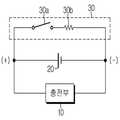
도 1은 본 발명의 일 실시예에 따른 과충전 방지 회로를 나타내는 도면으로서, 화학적 스위칭 소자가 적용된 과충전 방지 회로의 회로 구성도이다.
도 2는 도 1에 나타난 화학적 스위칭 소자의 내부 구조를 나타낸 단면도이다.
도 3은 본 발명의 다른 실시예에 따른 과충전 방지 회로를 나타내는 도면으로서, 병렬로 연결된 복수개의 화학적 스위칭 소자가 적용된 과충전 방지 회로의 회로 구성도이다.
도 4는 본 발명의 또 다른 실시예에 따른 과충전 방지 회로를 나타내는 도면으로서, 화학적 스위칭 소자와 직렬로 연결되며 이차전지와는 병렬로 연결되는 저항이 적용된 과충전 방지 회로의 회로 구성도이다.
도 5는 본 발명의 또 다른 실시예에 따른 과충전 방지 회로를 나타내는 도면으로서, 화학적 스위칭 소자 및 이차전지와 충전부 사이에 연결되는 저항이 적용된 과충전 방지 회로의 회로 구성도이다.
도 6은 본 발명의 또 다른 실시예에 따른 과충전 방지 회로를 나타내는 도면으로서, 퓨즈부가 적용된 과충전 방지 회로를 나타내는 회로 구성도이다.BRIEF DESCRIPTION OF THE DRAWINGS The accompanying drawings, which are incorporated in and form a part of the specification, illustrate exemplary embodiments of the invention and, together with the description, serve to explain the principles of the invention. And shall not be construed as limited to such matters.
1 is a circuit diagram of an overcharge protection circuit according to an embodiment of the present invention, which is an overcharge protection circuit to which a chemical switching element is applied.
2 is a cross-sectional view showing the internal structure of the chemical switching device shown in Fig.
FIG. 3 is a circuit diagram of an overcharge protection circuit according to another embodiment of the present invention, in which a plurality of chemical switching elements connected in parallel are applied. FIG.
FIG. 4 is a circuit diagram of an overcharge protection circuit according to another embodiment of the present invention, which is connected in series with a chemical switching device and is connected in parallel with a secondary battery.
FIG. 5 is a circuit diagram of an overcharge protection circuit according to another embodiment of the present invention, in which a chemical switching element and a resistor connected between a secondary battery and a live part are applied. FIG.
6 is a circuit diagram showing an overcharge protection circuit according to another embodiment of the present invention, showing an overcharge protection circuit to which a fuse section is applied.
이하, 첨부된 도면을 참조하여 본 발명의 바람직한 실시예를 상세히 설명하기로 한다. 이에 앞서, 본 명세서 및 청구범위에 사용된 용어나 단어는 통상적이거나 사전적인 의미로 한정해서 해석되어서는 아니 되며, 발명자는 그 자신의 발명을 가장 최선의 방법으로 설명하기 위해 용어의 개념을 적절하게 정의할 수 있다는 원칙에 입각하여 본 발명의 기술적 사상에 부합하는 의미와 개념으로 해석되어야만 한다. 따라서, 본 명세서에 기재된 실시예와 도면에 도시된 구성은 본 발명의 가장 바람직한 일부 실시예에 불과할 뿐이고 본 발명의 기술적 사상을 모두 대변하는 것은 아니므로, 본 출원시점에 있어서 이들을 대체할 수 있는 다양한 균등물과 변형예들이 있을 수 있음을 이해하여야 한다.Hereinafter, preferred embodiments of the present invention will be described in detail with reference to the accompanying drawings. Prior to this, terms and words used in the present specification and claims should not be construed as limited to ordinary or dictionary terms, and the inventor should appropriately interpret the concepts of the terms appropriately It should be interpreted in accordance with the meaning and concept consistent with the technical idea of the present invention based on the principle that it can be defined. Therefore, the embodiments described in the present specification and the configurations shown in the drawings are only some of the most preferred embodiments of the present invention and do not represent all the technical ideas of the present invention. Therefore, It is to be understood that equivalents and modifications are possible.
먼저 도 1 및 도 2를 참조하여 본 발명의 일 실시예에 따른 과충전 방지 회로를 설명하기로 한다.First, an overcharge prevention circuit according to an embodiment of the present invention will be described with reference to FIGS. 1 and 2. FIG.
도 1을 참조하면, 본 발명의 일 실시예에 따른 과충전 방지 회로는 충전부(10), 이차전지(20) 및 우회 회로부(30)를 포함한다.Referring to FIG. 1, an overcharge protection circuit according to an embodiment of the present invention includes a
상기 충전부(10)는 이차전지(20)와 함께 충전 시스템을 구성하며, 이차전지(20)의 양 단에 충전 전압을 인가하고 충전 전류를 공급함으로써 이차전지(20)를 충전하는 역할을 한다.The
상기 이차전지(20)는 3.7 내지 4.2V의 사용 전압 대역을 가진다. 상기 충전부(10)는 이차전지(20)가 상기 적정 전압 범위를 넘어 과충전 되지 않도록 충전 전압 및 충전 전류를 제어하는 제어 회로(미도시)를 구비한다. 즉, 상기 제어 회로는 이차전지(20)의 충전 전압이 미리 설정된 임계 값(Vmax,이차전지의 만충전 전압 이상의 값에 해당) 이상으로 상승하면 충전부(10)가 이차전지(20)에 더 이상 충전 전류를 공급하지 않도록 제어 한다.The
또한, 상기 이차전지(20) 역시 과충전, 과방전, 과전류, 과열 등을 감지하여 이차전지(20)의 동작을 차단하는 보호 회로를 구비하는 배터리 관리 장치(미도시), 즉 BMS(Battery Management System)와 결합된다.The
상기 제어 회로와 상기 배터리 관리 장치는 이차전지 기술 분야에서 자명한 기술에 해당하므로 더 이상의 자세한 설명은 생략하기로 한다.Since the control circuit and the battery management device correspond to technologies that are obvious in the secondary battery technology field, detailed description thereof will be omitted.
상기 우회 회로부(30)는 이차전지(20)와 병렬로 연결되며, 이차전지(20)의 충전 전압이 상기 임계 값(Vmax) 이상으로 상승할 경우 충전 전류의 전부 또는 일부를 우회시킴으로써 이차전지(20)를 과충전으로부터 보호하는 역할을 한다. 이를 위해, 상기 우회 회로부(30)는 이차전지(20)의 양 단에 상기 임계 값(Vmax) 이상의 전위차가 형성될 경우 통전되는 화학적 스위칭 소자(30a)를 포함한다.The
도 2는 상기 화학적 스위칭 소자(30a)의 내부 구조를 도시한 단면도이다.2 is a cross-sectional view showing the internal structure of the
도 2를 참조하면, 상기 화학적 스위칭 소자(30a)는 제1 도전 플레이트(31), 제2 도전 플레이트(32), 분리 막(33), 케이스(34), 전해액(35) 및 가변 물질(36)을 포함한다.2, the
상기 제1 도전 플레이트(31) 및 제2 도전 플레이트(32)는 도선(37)을 통해 각각 이차전지(20)의 일 단 및 타 단과 연결된다. 따라서 상기 제1 도전 플레이트(31) 및 제2 도전 플레이트(32) 사이에는 이차전지(20)의 충전 전압에 대응하는 전압이 인가된다. 또한 상기 제1 도전 플레이트(31) 및 제2 도전 플레이트(32)는 비 통전 상태에서 전기적 절연을 확보하기 위해 일정한 간극을 두고 배치된다.The first
상기 도전 플레이트(31,32)는 필요에 따라 그 면적이 달라질 수 있다. 면적의 변화는 화학적 스위칭 소자(30a)의 저항 특성에 영향을 미쳐 우회 회로부(30)를 통하여 흐르는 충전 전류의 량을 변화시킨다. 즉, 상기 도전 플레이트(31,32)의 면적이 넓어지면 화학적 스위칭 소자(30a)의 자체 저항이 낮아진다. 그 결과, 화학적 스위칭 소자(30a)가 통전되었을 때 충전 전류 중 비교적 많은 비율의 전류가 우회 회로부(30)를 통하여 흐르게 된다. 반면, 상기 도전 플레이트(31,32)의 면적이 작아지면 화학적 스위칭 소자(30a)의 자체 저항이 높아진다. 그 결과, 화학적 스위칭 소자(30a)가 통전되었을 때 충전 전류 중 비교적 적은 비율의 전류만이 우회 회로부(30)를 통해 흐르게 된다.The areas of the
한편, 상기 이차 전지(20)의 보호라는 관점에서 보면 이차전지(20)가 과충전 상태가 되면 충전 전류의 대부분이 우회 회로부(30)를 통해 흐르는 것이 바람직하다. 하지만 우회 회로부(30)를 통해 흐르는 충전 전류의 크기가 클 경우 화학적 스위칭 소자(30a)가 손상될 위험이 있다. 따라서, 도전 플레이트(31,32)의 면적 조절을 통해 상기 화학적 스위칭 소자(30a)의 자체 저항을 적절한 범위로 조절하는 것이 바람직하다.From the viewpoint of protection of the
상기 분리 막(33)은 다공성의 분리 막으로서 리튬 이차전지에 일반적으로 적용되는 폴리올레핀 계열의 분리 막이 사용될 수 있는데 본 발명이 이에 한하는 것은 아니다. 상기 분리 막(33)은 제1 도전 플레이트(31)와 제2 도전 플레이트(32) 사이에 개재되어 제1 도전 플레이트(31) 및 제2 도전 플레이트(32)가 물리적으로 서로 접촉되는 것을 방지한다.The
한편, 도 2에는, 분리 막(33)과 도전 플레이트(31,32) 사이에 간극이 존재하는 것으로 도시되어 있다. 하지만, 분리 막(33)과 도전 플레이트(31,32)가 서로 접촉하고 있는 경우도 본 발명의 범위에 포함되는 것은 자명하다.On the other hand, FIG. 2 shows that there is a gap between the separating
상기 케이스(34)는 도전 플레이트(31,32) 및 분리 막(33)을 수용한 채로 밀봉되며, 그 내부에는 전해액(35) 및 액상의 가변 물질(36)이 충진된다.The
상기 전해액(35)으로는 리튬 이차전지에 일반적으로 적용되는 것으로서 BF4-, Cl-, Br-, I-, ClO4- 등과 같은 음이온이나 이들의 조합으로 이루어진 이온을 포함하는 염이 프로필렌 카보네이트(Propylene carbonate, PC), 에틸렌 카보네이트(Ethylene carbonate, EC), 디에틸 카보네이트(Diethyl carbonate, DEC), 디메틸 카보네이트(Dimethyl carbonate, DMC), 디프로필 카보네이트(Dipropyl carbonate, DPC) 등의 유기 용매 또는 이들의 혼합물로 이루어진 유기 용매에 용해 및 해리된 것이 사용될 수 있다.As the
상기 가변 물질(36)은 이차전지(20)의 제1 도전 플레이트(31) 및 제2 도전 플레이트(32) 사이에 인가되는 전위차가 임계 값(Vmax) 미만인 경우에는 통전되지 않는 특성을 갖는다. 반면, 이차전지(20)가 과충전되어 제1 도전 플레이트(31) 및 제2 도전 플레이트(32) 사이에 임계 값(Vmax) 이상의 전위차가 인가되는 경우에는 통전 화학반응을 통해 전도성을 띠는 특성을 갖는다. 이러한 특성을 갖는 가변 물질(35)의 예로서 할로겐기가 치환된 톨루엔(Halogenated toluene), 바이페닐(Biphenyl), 사이클로헥실 벤젠 (Cyclohexyl benzene) 등을 들 수 있다.The
상기 할로겐기가 치환된 톨루엔 중에서도 특히 4-클로로톨루엔(4-chlorotoluene, 4CT)은 도전 플레이트(31,32) 사이에 4.75V 이상의 전위차가 형성되면 중합 반응(Polymerization)을 일으켜, 전도성을 가지게 된다. 따라서, 상기 가변 물질(36)로 4-클로로톨루엔을 사용하는 경우 이차전지(20)의 충전 전압이 점점 상승하여 4.75V에 이르게 되면 우회 회로부(30)를 통해 충전 전류의 전부 또는 일부가 흐르게 되므로 이차전지(20)가 과충전되는 것을 방지할 수 있다.Among the toluene substituted with the halogen group, 4-chlorotoluene (4CT) causes polymerization reaction when the potential difference of 4.75 V or more is formed between the
상기 바이페닐 및 사이클로헥실 벤젠은 도전 플레이트(31,32) 사이에 각각 4.6V 및 4.7V 이상의 전위차가 형성되면 중합 반응을 일으켜 전도성을 가지게 된다. 따라서, 상기 가변 물질(36)로 바이페닐 또는 사이클로헥실 벤젠을 사용하는 경우 이차전지(20)의 충전 전압이 점점 상승하여 4.6V 또는 4.7V 에 이르게 되면 우회 회로부(30)를 통해 충전 전류의 전부 또는 일부가 흐르게 되므로 이차전지(20)의 과충전을 방지할 수 있다.When biphenyl and cyclohexylbenzene have a potential difference of 4.6 V and 4.7 V or more between the
상기 가변 물질(36)은 할로겐기가 치환된 톨루엔 및 바이페닐, 사이클로헥실 벤젠으로만 한정되지 않는다. 따라서, 도전 플레이트(31,32) 사이에 일정 값 이상의 전위차가 형성되는 경우에 통전 화학반응을 통해 도전성을 갖는 화합물이라면 가변 물질(36)로서 얼마든지 사용이 가능하다. 다만, 상기 가변 물질(36)의 선택 시에는 이차전지(20)의 충전 상한 전압을 고려하여 4.2 내지 5.4V 의 범위에서 통전 화학반응을 일으키는 물질을 선택하는 것이 바람직하다.The
한편, 도 2에서는 상기 가변 물질(36)이 입자의 형태로 전해액(35)에 분산되어 있는 것처럼 도시되어 있다. 하지만 이는 도면 도시상의 편의를 위한 것이며 실제로는 가변 물질(36)이 전해액(35)에 고르게 혼합된 형태로 존재하는 것임은 자명하다.On the other hand, in FIG. 2, the
상술한 바와 같이 본 발명의 일 실시예에 따른 과충전 방지 회로는 우회 회로부(30)를 구비함으로써 이차전지(20)의 충전 전압이 임계 값(Vmax) 이상으로 상승할 경우 이차전지(20)로 유입되는 충전 전류를 우회시킴으로써 이차전지(20)의 과충전을 방지하는 효과를 가져온다.Overcharge protection in accordance with one embodiment of the present invention as described above, the circuit is a rechargeable battery (20) if the terminal voltage of the
다음은, 도 3을 참조하여 본 발명의 다른 실시예에 따른 과충전 방지 회로를 설명하기로 한다.Next, an overcharge prevention circuit according to another embodiment of the present invention will be described with reference to FIG.
도 3에 도시된 과충전 방지 회로는 도 1에 도시된 과충전 방지 회로와 비교할 때, 우회 회로부(30)에 적용되는 화학적 스위칭 소자(30a)가 복수개라는 점이 다를 뿐 다른 구성요소들은 동일하다. 따라서, 중복되는 설명은 생략하기로 하며, 복수개의 화학적 스위칭 소자(30a)가 연결된 구성 및 그 기능을 위주로 설명하기로 한다.The overcharge prevention circuit shown in Fig. 3 is the same as the overcharge protection circuit shown in Fig. 1 except that there are a plurality of
도 3을 참조하면, 본 발명의 다른 실시예에 따른 과충전 방지 회로는 서로 병렬로 연결된 복수개의 화학적 스위칭 소자(30a)가 적용된 구성을 갖는다.Referring to FIG. 3, the overcharge prevention circuit according to another embodiment of the present invention has a configuration in which a plurality of
상기 병렬로 연결된 복수개의 화학적 스위칭 소자(30a) 각각의 양 단에 걸리는 전압은 동일하므로 우회 회로부(30)의 통전 조건은 앞선 실시예의 경우와 동일하다. 다만, 상기 우회 회로부(30)가 통전 되었을 때 화학적 스위칭 소자(30a) 각각에 흐르는 우회 전류 값은 우회 회로부(30)에 유입되는 전류 값을 병렬로 연결된 화학적 스위칭 소자(30a)의 개수로 나눈 값에 해당하게 된다.Since the voltages applied to both ends of each of the plurality of
따라서, 병렬로 연결된 복수개의 화학적 스위칭 소자(30a)는 우회 회로부(30)가 통전될 때 흐르는 우회 전류를 분산시킴으로써, 우회 전류에 의해 화학적 스위칭 소자(30a)가 손상되는 것을 방지하는 효과를 가져온다.Therefore, the plurality of
다음은, 도 4를 참조하여 본 발명의 또 다른 실시예에 따른 과충전 방지 회로를 설명하기로 한다.Next, an overcharge prevention circuit according to another embodiment of the present invention will be described with reference to FIG.
도 4에 도시된 과충전 방지 회로는 도 1에 도시된 과충전 방지 회로와 비교할 때, 상기 우회 회로부(30)가 적어도 하나 이상의 제1 저항(30b)을 더 포함한다는 점만 다르고 다른 구성요소들은 동일하다.The overcharge prevention circuit shown in Fig. 4 differs from the overcharge prevention circuit shown in Fig. 1 in that the
상기 제1 저항(30b)은 화학적 스위칭 소자(30a)와는 직렬로 연결되고 이차전지(20)와는 병렬로 연결되어 우회 회로부(30)가 통전되었을 때 우회 회로부(30)로 유입되는 전류량을 조절하는 역할을 한다. 즉, 상기 화학적 스위칭 소자(30a)의 자체 저항 값이 매우 낮은 경우 제1 저항(30b)이 우회 회로부(30)를 통해 흐르는 전류의 크기를 일정한 범위로 제한하여 화학적 스위칭 소자(30a)의 손상을 방지한다.The
다음은, 도 5를 참조하여 본 발명의 또 다른 실시예에 따른 과충전 방지 회로를 설명하기로 한다.Next, an overcharge prevention circuit according to another embodiment of the present invention will be described with reference to FIG.
도 5에 도시된 과충전 방지 회로는 도 1에 도시된 과충전 방지 회로와 비교할 때, 적어도 하나 이상의 제2 저항(40)을 더 포함하는 점만 다르고 다른 구성요소들은 동일하다.The overcharge protection circuit shown in Fig. 5 differs from the overcharge protection circuit shown in Fig. 1 in that it further includes at least one
상기 제2 저항(40)은 화학적 스위칭 소자(30a) 및 이차전지(20)와 충전부(10) 사이에 직렬로 연결된다. 이 경우, 상기 제2 저항(40)의 저항 값을 크게 함으로써 우회 회로부(30)의 통전 시 충전 전류의 대부분이 우회 회로부(30)로 유입되도록 함과 동시에 회로에 흐르는 전류의 크기를 줄여주는 것이 가능하다.The
다음은, 도 6을 참조하여 본 발명의 또 다른 실시예에 따른 과충전 보호 회로를 설명하기로 한다.Next, an overcharge protection circuit according to another embodiment of the present invention will be described with reference to FIG.
도 6에 도시된 과충전 보호 회로는 도 1에 도시된 과충전 방지 회로와 비교할 때, 퓨즈부(50)를 더 포함하는 점만 다르고 다른 구성요소들은 동일하다.상기 퓨즈부(50)는 상기 화학적 스위칭 소자(30a) 및 이차전지(20)와 충전부(10) 사이에 직렬로 연결된다. 상기 퓨즈부(50)는 우회 회로부(30)에 흐르는 전류의 크기가 급격하게 상승할 경우 비가역적으로 파단됨으로써 과충전 방지 회로상의 전류의 흐름을 완전히 차단하는 역할을 한다.The overcharge protection circuit shown in Fig. 6 differs from the overcharge prevention circuit shown in Fig. 1 in that it further includes the
상기 퓨즈부(50)는 과충전 방지 회로를 구성하는 도선보다 낮은 용융점을 갖는 금속으로 이루어지는 것이 바람직하다. 또한, 상기 퓨즈부(50)의 파단 조건은 우회 회로부(30)를 통해 900 내지 1500A 의 크기를 가진 과전류가 흐를 때 파단되도록 선택하는 것이 바람직하다.It is preferable that the
이상에서 본 발명은 비록 한정된 실시예와 도면에 의해 설명되었으나, 본 발명은 이것에 의해 한정되지 않으며 본 발명이 속하는 기술분야에서 통상의 지식을 가진 자에 의해 본 발명의 기술사상과 아래에 기재될 특허청구범위의 균등범위 내에서 다양한 수정 및 변형이 가능함은 물론이다.While the present invention has been particularly shown and described with reference to exemplary embodiments thereof, it is to be understood that the invention is not to be limited to the details thereof and that various changes and modifications will be apparent to those skilled in the art. And various modifications and variations are possible within the scope of the appended claims.
10: 충전부20: 이차전지
30: 우회 회로부30a: 화학적 스위칭 소자
31: 제1 도전 플레이트32: 제2 도전 플레이트
33: 분리 막34: 케이스
35: 전해액36: 가변 물질
30b: 제1 저항40: 제2 저항
50: 퓨즈부10: charger 20: secondary battery
30:
31: first conductive plate 32: second conductive plate
33: separator 34: case
35: electrolyte 36: variable material
30b: first resistor 40: second resistor
50: Fuse section
Claims (17)
Translated fromKorean상기 우회 회로부는, 상기 이차전지와 병렬로 연결되고 이차전지의 충전 전압이 임계 값(Vmax) 이상이 되면 통전 화학반응을 일으키는 화학적 스위칭 소자; 및 상기 우회 회로부 상에서 화학적 스위칭 소자 및 이차전지와 직렬로 연결된 퓨즈부를 포함하고,
상기 화학적 스위칭 소자는, 상기 이차전지의 일 단과 연결되는 제1 도전 플레이트; 상기 이차전지의 타 단과 연결되며 상기 제1 도전 플레이트와 이격된 제2 도전 플레이트; 상기 제1 도전 플레이트와 제2 도전 플레이트 사이에 개재되는 분리 막; 상기 제1 도전 플레이트 및 제2 도전 플레이트 사이에 충진되며 상기 이차전지의 충전 전압이 임계 값(Vmax) 이상이 되면 상기 통전 화학 반응을 일으켜 전도성을 갖는 가변 물질; 및 상기 제1 도전 플레이트 및 상기 제2 도전 플레이트를 수용하는 케이스를 포함하는 것을 특징으로 하는 과충전 방지 회로.An overcharge prevention circuit for preventing overcharging of a secondary battery by flowing at least a part of a charging current flowing from a charging unit into a secondary battery when the secondary battery is overcharged to a bypass circuit unit,
The bypass circuit is chemically switching element connected in parallel with said secondary battery is caused to energize a chemical reaction the terminal voltage of the secondary battery when the threshold value (Vmax) or greater; And a fuse portion connected in series with the chemical switching device and the secondary battery on the bypass circuit portion,
The chemical switching device includes: a first conductive plate connected to one end of the secondary battery; A second conductive plate connected to the other end of the secondary battery and spaced apart from the first conductive plate; A separator interposed between the first conductive plate and the second conductive plate; A variable material filled between the first conductive plate and the second conductive plate and having conductivity when the charging voltage of the secondary battery becomes equal to or higher than a threshold value Vmax , And a case accommodating the first conductive plate and the second conductive plate.
상기 화학적 스위칭 소자는,
상기 케이스 내에 충진되는 전해액을 더 포함하는 것을 특징으로 하는 과충전 방지 회로.The method according to claim 1,
The chemical switching device includes:
And an electrolytic solution filled in the case.
상기 가변 물질은 할로겐기가 치환된 톨루엔(Halogenated toluene)인 것을 특징으로 하는 과충전 방지 회로.The method according to claim 1,
Wherein the variable material is a halogenated toluene substituted with a halogen group.
상기 가변 물질은 4-클로로톨루엔(4-chlorotoluene)인 것을 특징으로 하는 과충전 방지 회로.6. The method of claim 5,
Wherein the variable material is 4-chlorotoluene.
상기 임계 값(Vmax)은 4.75V 인 것을 특징으로 하는 과충전 방지 회로.The method according to claim 6,
The threshold value (Vmax) is the overcharge protection circuit, characterized in that 4.75V.
상기 가변 물질은 바이페닐(Biphenyl)인 것을 특징으로 하는 과충전 방지 회로.The method according to claim 1,
Wherein the variable material is biphenyl.
상기 임계 값(Vmax)은 4.6V 인 것을 특징으로 하는 과충전 방지 회로.9. The method of claim 8,
The threshold value (Vmax) is the overcharge protection circuit, characterized in that 4.6V.
상기 가변 물질은 사이클로헥실 벤젠(Cyclohexyl benzene)인 것을 특징으로 하는 과충전 방지 회로.The method according to claim 1,
Characterized in that the variable material is cyclohexyl benzene.
상기 임계 값(Vmax)은 4.7V 인 것을 특징으로 하는 과충전 방지 회로.11. The method of claim 10,
The threshold value (Vmax) is the overcharge protection circuit, characterized in that 4.7V.
상기 화학적 스위칭 소자는 복수개이며,
상기 복수개의 화학적 스위칭 소자는 서로 병렬로 연결된 것을 특징으로 하는 과충전 방지 회로.The method according to claim 1,
Wherein the chemical switching elements are plural,
Wherein the plurality of chemical switching elements are connected in parallel with each other.
상기 우회 회로부는,
상기 화학적 스위칭 소자와 직렬로 연결되며 상기 이차전지와 병렬로 연결되는 적어도 하나의 저항을 더 포함하는 것을 특징으로 하는 과충전 방지 회로.The method according to claim 1,
The bypass circuit unit includes:
Further comprising at least one resistor connected in series with the chemical switching device and connected in parallel with the secondary battery.
상기 퓨즈부는 상기 과충전 방지 회로상의 도선보다 낮은 용융점을 갖는 것을 특징으로 하는 과충전 방지 회로.The method according to claim 1,
Wherein the fuse portion has a lower melting point than a conductor on the overcharge protection circuit.
Priority Applications (1)
| Application Number | Priority Date | Filing Date | Title |
|---|---|---|---|
| KR1020120011429AKR101603626B1 (en) | 2012-02-03 | 2012-02-03 | Protective circuit for preventing overcharge |
Applications Claiming Priority (1)
| Application Number | Priority Date | Filing Date | Title |
|---|---|---|---|
| KR1020120011429AKR101603626B1 (en) | 2012-02-03 | 2012-02-03 | Protective circuit for preventing overcharge |
Publications (2)
| Publication Number | Publication Date |
|---|---|
| KR20130090255A KR20130090255A (en) | 2013-08-13 |
| KR101603626B1true KR101603626B1 (en) | 2016-03-15 |
Family
ID=49215940
Family Applications (1)
| Application Number | Title | Priority Date | Filing Date |
|---|---|---|---|
| KR1020120011429AActiveKR101603626B1 (en) | 2012-02-03 | 2012-02-03 | Protective circuit for preventing overcharge |
Country Status (1)
| Country | Link |
|---|---|
| KR (1) | KR101603626B1 (en) |
Cited By (1)
| Publication number | Priority date | Publication date | Assignee | Title |
|---|---|---|---|---|
| US11695172B2 (en) | 2017-04-03 | 2023-07-04 | Lg Energy Solution, Ltd. | Heat dissipating structure of cylindrical battery cell |
Families Citing this family (1)
| Publication number | Priority date | Publication date | Assignee | Title |
|---|---|---|---|---|
| KR102236055B1 (en)* | 2016-11-02 | 2021-04-05 | 주식회사 엘지화학 | Battery Module Comprising Circuit for Preventing Over-Charge |
Citations (2)
| Publication number | Priority date | Publication date | Assignee | Title |
|---|---|---|---|---|
| JP2005516378A (en) | 2001-06-20 | 2005-06-02 | シタラ リミティド | Thin planar switch and its application |
| JP2008103330A (en)* | 2006-10-17 | 2008-05-01 | Samsung Sdi Co Ltd | Electrolytic solution for high voltage lithium secondary battery and high voltage lithium secondary battery using the same |
Family Cites Families (3)
| Publication number | Priority date | Publication date | Assignee | Title |
|---|---|---|---|---|
| KR20060094717A (en)* | 2005-02-25 | 2006-08-30 | 주식회사 엘지화학 | Battery overcharge protection circuit |
| KR100907774B1 (en)* | 2005-03-30 | 2009-07-15 | 다이킨 고교 가부시키가이샤 | Electrolyte |
| KR20070033853A (en) | 2005-09-22 | 2007-03-27 | 주식회사 엘지화학 | Safety element for preventing overcharge of secondary battery and secondary battery combined with safety element |
- 2012
- 2012-02-03KRKR1020120011429Apatent/KR101603626B1/enactiveActive
Patent Citations (2)
| Publication number | Priority date | Publication date | Assignee | Title |
|---|---|---|---|---|
| JP2005516378A (en) | 2001-06-20 | 2005-06-02 | シタラ リミティド | Thin planar switch and its application |
| JP2008103330A (en)* | 2006-10-17 | 2008-05-01 | Samsung Sdi Co Ltd | Electrolytic solution for high voltage lithium secondary battery and high voltage lithium secondary battery using the same |
Cited By (1)
| Publication number | Priority date | Publication date | Assignee | Title |
|---|---|---|---|---|
| US11695172B2 (en) | 2017-04-03 | 2023-07-04 | Lg Energy Solution, Ltd. | Heat dissipating structure of cylindrical battery cell |
Also Published As
| Publication number | Publication date |
|---|---|
| KR20130090255A (en) | 2013-08-13 |
Similar Documents
| Publication | Publication Date | Title |
|---|---|---|
| KR100485752B1 (en) | Secondary Battery Protection Device | |
| EP2339672B1 (en) | Battery module and battery pack using same | |
| US8355231B2 (en) | Apparatus and method for protecting battery pack by detecting destruction of sense resistor in battery pack | |
| KR100929036B1 (en) | Protection circuit of battery pack, battery pack having same and operation method thereof | |
| US9130383B2 (en) | Charging/discharging control device, battery pack, electrical equipment, and charging/discharging control method | |
| KR101223730B1 (en) | Secondary battery pack and protection circuit module for the same | |
| KR101383167B1 (en) | Battery Pack of Improved Safety | |
| JP4659886B2 (en) | Secondary battery protection circuit | |
| KR20190028200A (en) | Battery module with a structure to break a connector using venting gas | |
| EP3300135B1 (en) | Battery module comprising wire-fixing ribs | |
| JP2014512089A (en) | Battery pack with improved safety | |
| KR102249889B1 (en) | Protection apparutus for rechargeable battery | |
| KR20150057732A (en) | Protection apparutus for rechargeable battery | |
| EP4156373B1 (en) | Battery and battery apparatus | |
| EP1787339A1 (en) | Safety device for preventing overcharge and secondary battery therewith | |
| EP1805829B8 (en) | Secondary battery having constant-voltage device | |
| KR101603626B1 (en) | Protective circuit for preventing overcharge | |
| KR20150045241A (en) | Battery cell equipped with disconnection device, and Battery module and Battery pack comprising the same | |
| CN105518956A (en) | Devices for preventing battery overcharging | |
| KR20180025702A (en) | Protection apparatus for rechargeable battery | |
| KR101486927B1 (en) | Battery module and terminal assembly applied for the same | |
| KR101262879B1 (en) | Apparatus and method for protecting battery pack by detecting swelling phenomenon of battery cell | |
| KR102320109B1 (en) | Battery module and method for manufacturing the same | |
| KR20130090159A (en) | Protective circuit for preventing overcharge | |
| KR101542283B1 (en) | Charge protection apparatus for secondary bettery, charger and battery pack |
Legal Events
| Date | Code | Title | Description |
|---|---|---|---|
| PA0109 | Patent application | Patent event code:PA01091R01D Comment text:Patent Application Patent event date:20120203 | |
| PG1501 | Laying open of application | ||
| A201 | Request for examination | ||
| PA0201 | Request for examination | Patent event code:PA02012R01D Patent event date:20140806 Comment text:Request for Examination of Application Patent event code:PA02011R01I Patent event date:20120203 Comment text:Patent Application | |
| E902 | Notification of reason for refusal | ||
| PE0902 | Notice of grounds for rejection | ||
| AMND | Amendment | ||
| E601 | Decision to refuse application | ||
| PE0601 | Decision on rejection of patent | Patent event date:20151026 Comment text:Decision to Refuse Application Patent event code:PE06012S01D Patent event date:20150428 Comment text:Notification of reason for refusal Patent event code:PE06011S01I | |
| X091 | Application refused [patent] | ||
| AMND | Amendment | ||
| PX0901 | Re-examination | Patent event code:PX09011S01I Patent event date:20151026 Comment text:Decision to Refuse Application Patent event code:PX09012R01I Patent event date:20150622 Comment text:Amendment to Specification, etc. | |
| PX0701 | Decision of registration after re-examination | Patent event date:20151216 Comment text:Decision to Grant Registration Patent event code:PX07013S01D Patent event date:20151126 Comment text:Amendment to Specification, etc. Patent event code:PX07012R01I Patent event date:20151026 Comment text:Decision to Refuse Application Patent event code:PX07011S01I Patent event date:20150622 Comment text:Amendment to Specification, etc. Patent event code:PX07012R01I | |
| X701 | Decision to grant (after re-examination) | ||
| GRNT | Written decision to grant | ||
| PR0701 | Registration of establishment | Comment text:Registration of Establishment Patent event date:20160309 Patent event code:PR07011E01D | |
| PR1002 | Payment of registration fee | Payment date:20160309 End annual number:3 Start annual number:1 | |
| PG1601 | Publication of registration | ||
| FPAY | Annual fee payment | Payment date:20190116 Year of fee payment:4 | |
| PR1001 | Payment of annual fee | Payment date:20190116 Start annual number:4 End annual number:4 | |
| FPAY | Annual fee payment | Payment date:20200116 Year of fee payment:5 | |
| PR1001 | Payment of annual fee | Payment date:20200116 Start annual number:5 End annual number:5 | |
| PR1001 | Payment of annual fee | Payment date:20210302 Start annual number:6 End annual number:6 | |
| PR1001 | Payment of annual fee | Payment date:20211220 Start annual number:7 End annual number:7 | |
| PR1001 | Payment of annual fee | Payment date:20221226 Start annual number:8 End annual number:8 | |
| PR1001 | Payment of annual fee | Payment date:20231226 Start annual number:9 End annual number:9 |