KR101598075B1 - A semiconductor memory element having a single gate structure and a semiconductor memory element array having a single gate structure - Google Patents
A semiconductor memory element having a single gate structure and a semiconductor memory element array having a single gate structureDownload PDFInfo
- Publication number
- KR101598075B1 KR101598075B1KR1020090058284AKR20090058284AKR101598075B1KR 101598075 B1KR101598075 B1KR 101598075B1KR 1020090058284 AKR1020090058284 AKR 1020090058284AKR 20090058284 AKR20090058284 AKR 20090058284AKR 101598075 B1KR101598075 B1KR 101598075B1
- Authority
- KR
- South Korea
- Prior art keywords
- unit cell
- conductivity type
- gate
- well
- ion implantation
- Prior art date
- Legal status (The legal status is an assumption and is not a legal conclusion. Google has not performed a legal analysis and makes no representation as to the accuracy of the status listed.)
- Active
Links
- 239000004065semiconductorSubstances0.000titleclaimsabstractdescription73
- 238000005468ion implantationMethods0.000claimsabstractdescription32
- 239000000758substrateSubstances0.000claimsabstractdescription14
- 238000000034methodMethods0.000claimsdescription12
- 238000002955isolationMethods0.000claimsdescription5
- 239000011159matrix materialSubstances0.000claimsdescription3
- 125000006850spacer groupChemical group0.000claims1
- 230000010354integrationEffects0.000abstractdescription2
- 230000008878couplingEffects0.000description9
- 238000010168coupling processMethods0.000description9
- 238000005859coupling reactionMethods0.000description9
- 238000010586diagramMethods0.000description6
- 238000002347injectionMethods0.000description3
- 239000007924injectionSubstances0.000description3
- 230000006870functionEffects0.000description2
- 238000012986modificationMethods0.000description2
- 230000004048modificationEffects0.000description2
- 230000002093peripheral effectEffects0.000description2
- 230000000903blocking effectEffects0.000description1
- 230000000694effectsEffects0.000description1
- 239000002784hot electronSubstances0.000description1
Images


Classifications
- H—ELECTRICITY
- H10—SEMICONDUCTOR DEVICES; ELECTRIC SOLID-STATE DEVICES NOT OTHERWISE PROVIDED FOR
- H10B—ELECTRONIC MEMORY DEVICES
- H10B63/00—Resistance change memory devices, e.g. resistive RAM [ReRAM] devices
- H10B63/80—Arrangements comprising multiple bistable or multi-stable switching components of the same type on a plane parallel to the substrate, e.g. cross-point arrays
- H—ELECTRICITY
- H01—ELECTRIC ELEMENTS
- H01L—SEMICONDUCTOR DEVICES NOT COVERED BY CLASS H10
- H01L21/00—Processes or apparatus adapted for the manufacture or treatment of semiconductor or solid state devices or of parts thereof
- H01L21/02—Manufacture or treatment of semiconductor devices or of parts thereof
- H01L21/04—Manufacture or treatment of semiconductor devices or of parts thereof the devices having potential barriers, e.g. a PN junction, depletion layer or carrier concentration layer
- H01L21/18—Manufacture or treatment of semiconductor devices or of parts thereof the devices having potential barriers, e.g. a PN junction, depletion layer or carrier concentration layer the devices having semiconductor bodies comprising elements of Group IV of the Periodic Table or AIIIBV compounds with or without impurities, e.g. doping materials
- H01L21/26—Bombardment with radiation
- H01L21/263—Bombardment with radiation with high-energy radiation
- H01L21/265—Bombardment with radiation with high-energy radiation producing ion implantation
- H—ELECTRICITY
- H01—ELECTRIC ELEMENTS
- H01L—SEMICONDUCTOR DEVICES NOT COVERED BY CLASS H10
- H01L21/00—Processes or apparatus adapted for the manufacture or treatment of semiconductor or solid state devices or of parts thereof
- H01L21/02—Manufacture or treatment of semiconductor devices or of parts thereof
- H01L21/04—Manufacture or treatment of semiconductor devices or of parts thereof the devices having potential barriers, e.g. a PN junction, depletion layer or carrier concentration layer
- H01L21/18—Manufacture or treatment of semiconductor devices or of parts thereof the devices having potential barriers, e.g. a PN junction, depletion layer or carrier concentration layer the devices having semiconductor bodies comprising elements of Group IV of the Periodic Table or AIIIBV compounds with or without impurities, e.g. doping materials
- H01L21/28—Manufacture of electrodes on semiconductor bodies using processes or apparatus not provided for in groups H01L21/20 - H01L21/268
- H01L21/28008—Making conductor-insulator-semiconductor electrodes
- H01L21/28017—Making conductor-insulator-semiconductor electrodes the insulator being formed after the semiconductor body, the semiconductor being silicon
- H01L21/28026—Making conductor-insulator-semiconductor electrodes the insulator being formed after the semiconductor body, the semiconductor being silicon characterised by the conductor
- H01L21/28123—Lithography-related aspects, e.g. sub-lithography lengths; Isolation-related aspects, e.g. to solve problems arising at the crossing with the side of the device isolation; Planarisation aspects
- H01L21/28141—Lithography-related aspects, e.g. sub-lithography lengths; Isolation-related aspects, e.g. to solve problems arising at the crossing with the side of the device isolation; Planarisation aspects insulating part of the electrode is defined by a sidewall spacer, e.g. dummy spacer, or a similar technique, e.g. oxidation under mask, plating
- H—ELECTRICITY
- H10—SEMICONDUCTOR DEVICES; ELECTRIC SOLID-STATE DEVICES NOT OTHERWISE PROVIDED FOR
- H10D—INORGANIC ELECTRIC SEMICONDUCTOR DEVICES
- H10D84/00—Integrated devices formed in or on semiconductor substrates that comprise only semiconducting layers, e.g. on Si wafers or on GaAs-on-Si wafers
- H10D84/01—Manufacture or treatment
- H10D84/0123—Integrating together multiple components covered by H10D12/00 or H10D30/00, e.g. integrating multiple IGBTs
- H10D84/0126—Integrating together multiple components covered by H10D12/00 or H10D30/00, e.g. integrating multiple IGBTs the components including insulated gates, e.g. IGFETs
- H10D84/0147—Manufacturing their gate sidewall spacers
- H—ELECTRICITY
- H10—SEMICONDUCTOR DEVICES; ELECTRIC SOLID-STATE DEVICES NOT OTHERWISE PROVIDED FOR
- H10D—INORGANIC ELECTRIC SEMICONDUCTOR DEVICES
- H10D84/00—Integrated devices formed in or on semiconductor substrates that comprise only semiconducting layers, e.g. on Si wafers or on GaAs-on-Si wafers
- H10D84/01—Manufacture or treatment
- H10D84/0123—Integrating together multiple components covered by H10D12/00 or H10D30/00, e.g. integrating multiple IGBTs
- H10D84/0126—Integrating together multiple components covered by H10D12/00 or H10D30/00, e.g. integrating multiple IGBTs the components including insulated gates, e.g. IGFETs
- H10D84/0156—Manufacturing their doped wells
Landscapes
- Physics & Mathematics (AREA)
- Engineering & Computer Science (AREA)
- High Energy & Nuclear Physics (AREA)
- Condensed Matter Physics & Semiconductors (AREA)
- General Physics & Mathematics (AREA)
- Manufacturing & Machinery (AREA)
- Computer Hardware Design (AREA)
- Microelectronics & Electronic Packaging (AREA)
- Power Engineering (AREA)
- Health & Medical Sciences (AREA)
- Toxicology (AREA)
- Non-Volatile Memory (AREA)
Abstract
Translated fromKoreanDescription
Translated fromKorean실시예는 싱글 게이트 구조의 반도체 메모리 소자 및 싱글 게이트 구조의 반도체 메모리 소자 어레이에 관한 것이다.The embodiment relates to a semiconductor memory element of a single gate structure and a semiconductor memory element array of a single gate structure.
일반적으로, EPROM(Erasable Programmable Read Only Memory)과 같은 반도체 메모리 소자는 플로팅 게이트(Floating gate), ONO(Oxide-Nitride-Oxide)층, 컨트롤 게이트(Control gate)가 적층된 다중 폴리 구조를 가지나, 공정의 단순함, 동작 우수성 등의 특성을 보이는 싱글 게이트(single gate) 구조에 대한 연구가 진행중이다.2. Description of the Related Art In general, a semiconductor memory device such as an EPROM (Erasable Programmable Read Only Memory) has a multi-layered structure including a floating gate, an oxide-nitride-oxide (ONO) layer, and a control gate, And a single gate structure showing characteristics such as simplicity and operational superiority of the device is under development.
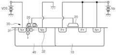
도 1은 일반적인 싱글 게이트 구조의 반도체 메모리 소자를 프로그램하는 경우의 전압 인가 형태를 도시한 도면인데, 이하의 설명에서 인용된 반도체 메모리 소자는 EPROM인 것으로 한다.1 is a diagram showing a voltage application mode when a semiconductor memory device of a general single gate structure is programmed. It is assumed that the semiconductor memory device cited in the following description is an EPROM.
상기 반도체 메모리 소자는 핫채널 전자 주입(Hot Channel Electron Injection) 방식으로 프로그램되며, N-웰(10; 컨트롤 게이트로 동작됨)에 프로그램 전압(Program Voltage; +Vp)이 인가되면 2개의 플로팅 게이트(20)의 커플링 비율(ratio)에 의하여 특정 전압이 유기된다.When the program voltage (+ Vp) is applied to the N-well 10 (operated as a control gate), the semiconductor memory device is programmed by a hot channel electron injection (Hot Channel Electron Injection) 20, the specific voltage is induced by the coupling ratio.
상기 플로팅 게이트(20)에 유기된 전압은 NMOS(30) 채널 영역의 전위를 반전시키고, 상기 NMOS(30)의 드레인(31)에 소정 전압(VDS)이 인가되면 상기 드레인(31)으로부터 소스(32) 측으로 전류가 흐른다.The voltage induced in the
따라서, 상기 드레인(31) 접합 영역 부근에서 발생되는 핫채널 전자가 상기 플로팅 게이트(20)로 주입되어 상기 NMOS(30)의 문턱 전압이 높아질 수 있다.Therefore, hot channel electrons generated near the junction region of the
도 2는 일반적인 싱글 게이트 구조의 반도체 메모리 소자의 데이터를 읽는(reading) 경우의 전압 인가 형태를 도시한 도면이다.FIG. 2 is a diagram showing a voltage application form when reading data of a semiconductor memory device of a general single gate structure. FIG.
상기 N-웰(10)에 읽기 전압(Reading Voltage; +VR)을 인가하면, 상기 플로팅 게이트(20)에 특정 전압이 유기된다. 또한, 상기 NMOS(30)의 드레인(31)에 읽기 동작을 위한 드레인 전압(Positive Drain Voltage)를 인가하고 상기 소스(32)는 그라운드시킨다.When a reading voltage (+ VR) is applied to the N-
상기 플로팅 게이트(20)에 전자가 주입되어 있고 상기 NMOS(30)의 문턱 전압이 높은 프로그램 상태이면, 상기 플로팅 게이트(20)에 유기된 특정 전압으로도 상기 NMOS(30)를 턴온(turn-on)시킬 수 없으므로 전류가 흐르지 않는다.The
또한, 상기 플로팅 게이트(20)로부터 전자가 빠져나가 있고 상기 NMOS(30)의 문턱 전압이 낮은 삭제 상태라면, 상기 플로팅 게이트(20)에 유기된 특정 전압으로 상기 NMOS(30)를 턴온시킬 수 있으므로 전류가 흐른다.Further, if the electrons have escaped from the
따라서, 각각의 경우에 따라 데이터를 읽을 수 있다.Therefore, the data can be read in each case.
이와 같은 일반적인 싱글 게이트 구조의 반도체 메모리 소자는 상기 NMOS(30)가 형성되어 프로그램/읽기 동작이 이루어지는 P-웰(40)이 반도체 기판과 전기적으로 연결되어 있다.In the conventional semiconductor memory device having a single gate structure, the P-
따라서, 도면에 도시되지 않았으나 상기 반도체 기판의 다른 영역에 소정 회로소자가 함께 구현되고, 이때 반도체 기판이 특정 음전위로 바이어스 된다면 상기 반도체 메모리 소자는 동작될 수 없다.Therefore, although not shown in the drawing, a predetermined circuit element is implemented together with another region of the semiconductor substrate, and the semiconductor memory element can not be operated if the semiconductor substrate is biased to a specific negative potential.
이렇게 반도체 기판이 음전위로 바이어스된 상태에서, 싱글 게이트 구조의 반도체 메모리 소자를 동작시키기 위하여 P-웰과 반도체 기판을 분리하는 Deep N-웰을 형성하는 방법이 있다.In a state where the semiconductor substrate is biased to a negative potential, there is a method of forming a Deep N-well for separating the P-well and the semiconductor substrate to operate the semiconductor memory device of the single gate structure.
그러나, 이때 싱글 게이트 구조의 반도체 메모리 소자의 워드 라인(word line) 역할을 하는 상기 N-웰(10)과 상기 Deep N-웰을 다시 분리시켜야 하므로 구현이 어렵고 동작이 불안정해지는 문제점이 있다.However, since the N-
또한, 상기 N-웰(10)은 상기 플로팅 게이트(20)를 특정 전위로 유기시키는 컨트롤 게이트로 기능되므로, 비트 라인(상기 NMOS(30)의 드레인(31)과 연결됨) 방향의 인접된 N-웰(10)과 격리되어야 한다.Since the N-well 10 functions as a control gate for causing the
따라서 반도체 메모리 소자의 셀(cell) 사이즈가 매우 커지고, 대용량 반도체 메모리 소자에 적용하기 힘들어지는 문제점이 있다.Therefore, the size of the cell of the semiconductor memory device becomes very large, which makes it difficult to apply it to a large-capacity semiconductor memory device.
실시예는 저전압 환경에서도 안정적으로 동작되고, 셀 사이즈 및 주변 회로 영역의 사이즈를 최소화할 수 있는 싱글 게이트 구조의 반도체 메모리 소자 및 싱글 게이트 구조의 반도체 메모리 소자 어레이를 제공한다.Embodiments provide a semiconductor memory device of a single gate structure and a semiconductor memory device array of a single gate structure that can be stably operated even under a low voltage environment and can minimize the size of a cell size and a peripheral circuit area.
실시예에 따른 싱글 게이트 구조의 반도체 메모리 소자는 반도체 기판의 상부에 나란히 형성된 제1도전형 웰 및 제2도전형 웰; 상기 제1도전형 웰 및 상기 제2도전형 웰 위에 각각 형성된 제1 게이트 및 제2 게이트; 상기 제1 게이트 일측의 상기 제1도전형 웰에 형성된 제2도전형 제1 이온주입영역 및 상기 제1 게이트 타측의 상기 제1도전형 웰에 형성된 제2도전형 제2 이온주입영역; 상기 제2 게이트 일측의 상기 제2도전형 웰에 형성된 제1도전형 제1 이온주입영역 및 상기 제2 게이트 타측의 상기 제2도전형 웰에 형성된 제1도전형 제2 이온주입영역을 포함한다.A semiconductor memory device of a single gate structure according to an embodiment includes: a first conductive well and a second conductive well formed side by side on a semiconductor substrate; A first gate and a second gate formed on the first conductive well and the second conductive well, respectively; A second conductivity type first ion implantation region formed in the first conductivity type well on one side of the first gate and a second conductivity type second ion implantation region formed in the first conductivity type well on the other side of the first gate; A first conductivity type first ion implantation region formed in the second conductivity type well at one side of the second gate and a first conductivity type second ion implantation region formed in the second conductivity type well at the other side of the second gate .
실시예에 따른 싱글 게이트 구조의 반도체 메모리 소자 어레이는 실시예에 따른 싱글 게이트 구조의 반도체 메모리 소자가 단위셀을 이루고, 상기 단위셀이 2×2 행렬을 이루어 4비트셀을 구성하며; 1행 1열의 제1 단위셀 및 1행 2열의 제2 단위셀은 X축 상에서 서로 마주하여 대칭 구조를 이루고, 2행 1열의 제3 단위셀 및 2행 2열의 제4 단위셀은 X축 상에서 서로 마주하여 대칭 구조를 이루며; 상기 제1 단위셀 및 상기 제3 단위셀은 Y축 상에서 나란히 배열되고, 상기 제2 단위셀 및 상기 제4 단위셀은 Y축 상에서 나란히 배열되는 것을 특징으로 한다.A single-gate semiconductor memory element array according to an embodiment of the present invention includes a semiconductor memory device of a single gate structure as a unit cell, and the unit cells form a 2x2 matrix to form a 4-bit cell; The first unit cell of the first row and the first column and the second unit cell of the first row and the second column are symmetrical with respect to each other on the X axis and the third unit cell of the second row and the first column and the fourth unit cell of the second row and the second column are arranged on the X axis Facing each other and forming a symmetrical structure; The first unit cell and the third unit cell are arranged side by side on the Y axis, and the second unit cell and the fourth unit cell are arranged side by side on the Y axis.
실시예에 의하면, 다음과 같은 효과가 있다.According to the embodiment, the following effects can be obtained.
첫째, 반도체 메모리 소자가 셀렉트 NMOS TR과 플로팅 PMOS TR이 직렬로 연결된 싱글 게이트 구조로 구현됨으로써, 반도체 메모리 소자의 크기를 최소화하고 셀의 집적도를 증가시킬 수 있다.First, since the semiconductor memory device is implemented as a single gate structure in which the select NMOS transistor and the floating PMOS transistor are connected in series, the size of the semiconductor memory device can be minimized and the degree of integration of the cell can be increased.
둘째, 반도체 메모리 소자의 프로그램, 리딩 동작이 저전압 환경에서도 안정적으로 이루어질 수 있으므로, 반도체 메모리 셀을 구동시키기 위한 주변회로를 단순화할 수 있고, 회로 영역의 사이즈를 최소화할 수 있다.Secondly, since the program and read operation of the semiconductor memory device can be stably performed in a low-voltage environment, the peripheral circuit for driving the semiconductor memory cell can be simplified, and the size of the circuit area can be minimized.
첨부된 도면을 참조하여 실시예에 따른 싱글 게이트 구조의 반도체 메모리 소자 및 싱글 게이트 구조의 반도체 메모리 소자 어레이에 대하여 상세히 설명한다.A semiconductor memory device of a single gate structure and a semiconductor memory device array of a single gate structure according to an embodiment will be described in detail with reference to the accompanying drawings.
이하, 실시예를 설명함에 있어, 관련된 공지 기능 또는 구성에 대한 구체적인 설명은 본 발명의 요지를 불필요하게 흐릴 수 있다고 판단되므로 본 발명의 기술적 사상과 직접적인 관련이 있는 핵심적인 구성부만을 언급하기로 한다.Hereinafter, a detailed description of known functions and configurations incorporated herein will be omitted when it may make the subject matter of the present invention unclear. Therefore, only the essential components directly related to the technical idea of the present invention will be described .
본 발명에 따른 실시 예의 설명에 있어서, 각 층(막), 영역, 패턴 또는 구조물들이 기판, 각 층(막), 영역, 패드 또는 패턴들의 "상/위(on)"에 또는 "아래(under)"에 형성되는 것으로 기재되는 경우에 있어, "상/위(on)"와 "아래(under)"는 "직접(directly)" 또는 "다른 층을 개재하여 (indirectly)" 형성되는 것을 모두 포함한다. 또한 각 층의 상/위 또는 아래에 대한 기준은 도면을 기준 으로 설명한다.In describing an embodiment according to the present invention, it is to be understood that each layer (film), region, pattern or structure may be referred to as being "on" or "under" Quot; on "and" under "refer to both " directly" or "indirectly & do. Also, the criteria for top, bottom, or bottom of each layer will be described with reference to the drawings.
도 3은 실시예에 따른 싱글 게이트 구조의 반도체 메모리 소자의 구조를 도시한 상면도이고, 도 4는 도 3의 표시선 A-A'를 기준으로 한 실시에에 따른 싱글 게이트 구조의 반도체 메모리 소자의 구조를 도시한 측단면도이다.FIG. 3 is a top view illustrating a structure of a semiconductor memory device of a single gate structure according to an embodiment. FIG. 4 is a cross-sectional view of a semiconductor memory device of a single gate structure according to an embodiment, Fig.
이하, 도 3 내지 도 4를 참조하여 실시예에 따른 싱글 게이트 구조의 반도체 메모리 소자에 대하여 설명하는데, 실시예에 따른 싱글 게이트 구조의 반도체 메모리 소자는 EPROM인 것으로 한다.Hereinafter, a semiconductor memory device having a single gate structure according to an embodiment will be described with reference to FIGS. 3 to 4. The semiconductor memory device having a single gate structure according to an embodiment is an EPROM.
도 3 및 도 4를 참조하면, 실시예에 따른 싱글 게이트 구조의 반도체 메모리 소자는 반도체 기판(100), 제1도전형 웰(105), 제2도전형 웰(110), 소자분리영역(115), 제2도전형 제1 이온주입영역(120), 제2도전형 제2 이온주입영역(125), 제1 게이트절연막(140), 제1 게이트(145), 제1도전형 제1 이온주입영역(130), 제1도전형 제2 이온주입영역(135), 제2 게이트절연막(150), 제2 게이트(155), 살리사이드 블럭층(Salicide blocking layer)(160), 제1탭(170), 제2탭(175), 제3탭(180), 제4탭(185)을 포함하여 구성된다.3 and 4, the semiconductor memory device of the single gate structure according to the embodiment includes a
도 3 및 도 4에 도시된 실시예에 따른 반도체 메모리 소자는 단위셀 영역만을 도시한 것이다.The semiconductor memory device according to the embodiment shown in FIGS. 3 and 4 shows only a unit cell region.
이하, 설명의 편의를 위하여 상기 제1도전형 웰(105), 제2도전형 웰(110), 제2도전형 제1 이온주입영역(120), 제2도전형 제2 이온주입영역(125), 제1도전형 제1 이온주입영역(130), 제1도전형 제2 이온주입영역(135)은 각각 "P웰(105)", "N웰(110)", "N소스 영역(120)", "N드레인 영역(125)", "P소스 영역(130)", "P드레인 영역(135)"으로 지칭한다.Hereinafter, for convenience of explanation, the first
이하의 설명에서, 상기 제1도전형은 P타입을 의미하고, 상기 제2도전형은 N타입을 의미하는 것으로 하였으나, 그 반대의 타입으로 해석될 수도 있다.In the following description, the first conductive type means the P type, and the second conductive type means the N type, but it may be interpreted as the opposite type.
이와 같은 실시예에 따른 반도체 메모리 소자는 셀렉트(select) 제2도전형 MOS 트랜지스터, 즉 셀렉트 NMOS TR"의 제1 영역(B)과, 플로팅(floating) 제1도전형 MOS 트랜지스터, 즉 "플로팅 PMOS TR"의 제2 영역(D)으로 구분될 수 있다.The semiconductor memory device according to this embodiment includes a first region B of a select second conductive type MOS transistor, that is, a select NMOS TR " and a floating first conductive type MOS transistor, Quot; and "TR ".
상기 반도체 기판(100), 가령 P형 서브(sub) 기판의 상부에 상기 P웰(105)과 상기 N웰(110)이 나란히 형성된다. 이때, 상기 P웰(105)과 상기 N웰(110)은 동일한 깊이로 형성되는 것이 좋다.The
상기 P웰(105)과 상기 N웰(110)은 상기 소자분리영역(115)에 의하여 이격될 수 있는데, 상기 소자분리영역(115)은 상기 P웰(105)과 N웰(110)을 완전히 이격시키거나 도 4에 도시된 것처럼 상측 일부만을 이격시킬 수도 있다.The
상기 P웰(105)은 상기 제1 영역(B)을 이루는 베이스층이 되고, 상기 N웰(110)은 상기 제2 영역(D)을 이루는 베이스층이 된다.The
상기 P웰(105)이 형성된 상기 반도체 기판(100) 위에 제1 게이트절연막(140)이 형성되고, 그 위로 제1 게이트(145)가 형성된다.A first
또한, 상기 제1 게이트(145) 일측의 상기 P웰(105) 상측에 상기 N소스 영역(120)이 형성되고, 상기 제1 게이트(145) 타측의 상기 P웰(105) 상측에 상기 N드레인 영역(125)이 형성된다.The
상기 N웰(110)이 형성된 상기 반도체 기판(100) 위에 제1 게이트절연막(150) 이 형성되고, 그 위로 제2 게이트(155)가 형성된다.A first
또한, 상기 제2 게이트(155) 일측의 상기 N웰(110) 상측에 상기 P소스 영역(130)이 형성되고, 상기 제2 게이트(155) 타측의 상기 N웰(110) 상측에 상기 P드레인 영역(135)이 형성된다.The
이와 같이 하여, 제1 영역(B)의 셀렉트 NMOS TR과 제2 영역(D)의 플로팅 PMOS TR가 형성되는데, 각각의 트랜지스터 영역에는 LDD(Lightly doped drain) 영역, 사이드월, 스페이서 등의 구조물이 더 포함될 수 있음은 물론이다.In this manner, the floating NMOS transistor TR of the first region B and the floating PMOS TR of the second region D are formed. In each transistor region, structures such as LDD (lightly doped drain) regions, sidewalls, Of course, be included.
상기 살리사이드 블럭층(160)은 상기 제2 게이트(155)를 적어도 포함하여 상기 제2 게이트(155) 위에 형성되며, 상기 제2 게이트(155)에 살리사이드가 형성되는 것을 방지한다.The
상기 N드레인 영역(125)과 상기 P소스 영역(130)은 상기 소자분리영역(115)에 의하여 이격된다.The
상기 제1탭(170), 상기 제2탭(175), 상기 제3탭(180), 상기 제4탭(185)은 각각 상기 N소스 영역(120), 상기 N드레인 영역(125), 상기 P소스 영역(130), 상기 P드레인 영역(135) 위에 형성되며, 전압 인가시 전극으로 이용되거나 본딩 패드로 이용될 수 있다.The
이하, 실시예에 따른 반도체 메모리 소자의 프로그램(program) 동작, 리딩(reading) 동작에 대하여 설명하면 다음과 같다.Hereinafter, a program operation and a reading operation of the semiconductor memory device according to the embodiment will be described.
상기 N소스 영역(120)은 공통 소스 라인(CSL; Common Source Line)과 연결되고, 상기 N드레인 영역(125)은 상기 P소스 영역(130)과 별도의 라인(C)을 통하여 연결된다.The
또한, 상기 제1 게이트(145)는 워드 라인(WL; Word Line)과 연결되고, 상기 제2 게이트(155)는 플로팅되며, 상기 P드레인 영역(135)은 비트 라인(BL; Bit Line)과 연결된다.The
따라서, 실시예에 따른 반도체 메모리 소자의 단위셀은 제1 영역(B)의 셀렉트 NMOS TR과 제2 영역(D)의 플로팅 PMOS TR이 직렬로 연결된 구조를 가지게 된다.Accordingly, the unit cell of the semiconductor memory device according to the embodiment has a structure in which the select NMOS transistor TR of the first region B and the floating PMOS TR of the second region D are connected in series.
실시예에 따른 반도체 메모리 소자의 단위셀이 프로그램되는 경우, 상기 비트 라인과 연결된 상기 P드레인 영역(135)과 상기 N웰(110)에 양전위의 제1전압(Vpp; Positive Program Vlotage)을 인가하고, 상기 워드 라인과 연결된 상기 제1 게이트(145)에 양전위의 제2전압(Vwlp; Program Word Line Voltage)을 인가한다.When a unit cell of the semiconductor memory device according to the embodiment is programmed, a positive voltage (Vpp) of positive potential is applied to the P-
상기 공통 소스 라인과 연결된 상기 N소스 영역(120)과 상기 P웰(105)은 약 0V가 인가된다.The
이때, 상기 제2 게이트(155)와 상기 P소스 영역(130) 사이에 제1 커플링 커패시턴스가 존재하고, 상기 제2 게이트(155)와 상기 P드레인 영역(135) 사이에 제2 커플링 커패시턴스가 존재하며, 상기 P소스 영역(130)과 상기 P드레인 영역(135) 사이의 채널 영역과 상기 제2 게이트(155) 사이에 제3 커플링 커패시턴스가 존재한다.A first coupling capacitance exists between the
이와 같은 바이어스(Bias) 조건에 의하면, 상기 N웰(110)과 상기 P드레인 영역(135)에 인가된 상기 제1전압에 의하여 상기 제3 커플링 커패시턴스가 상대적으 로 커지며, 상기 제2 게이트(155)에 소정의 양전위의 제3전압(Positive Voltage)이 발생된다.According to such a bias condition, the third coupling capacitance is relatively increased by the first voltage applied to the N well 110 and the
상기 제3전압의 영향에 의하여, 상기 제2 영역(D)의 플로팅 PMOS TR이 턴온(Turn-on)되고, 상기 제2전압에 의하여 상기 제1 영역(B)의 셀렉트 NMOS TR도 턴온됨으로써, 상기 P드레인 영역(135), 즉 상기 비트 라인으로부터 상기 N소스 영역(120), 즉 상기 공통 소스 라인으로 전류가 흐른다.The floating PMOS TR of the second region D is turned on by the influence of the third voltage and the select NMOS TR of the first region B is also turned on by the second voltage, Current flows from the
이와 같이, 상기 제1 영역(B)의 셀렉트 NMOS TR과 상기 제2 영역(D)의 플로팅 PMOS TR이 함께 턴온되면 상기 플로팅 PMOS TR의 상기 P드레인 영역(135) 부근에서 CHEI(Channel Hot Electron Injection) 현상이 발생하고, 상기 제2 게이트(155)에 전자가 추가적으로 주입된다.When the select NMOS transistor TR of the first region B and the floating PMOS transistor TR of the second region D are turned on together, a channel hot electron injection (CHEI) is performed in the vicinity of the
이로 인하여, 상기 플로팅 PMOS TR의 문턱 전압(Threshold Voltage)가 낮아지고, 상기 플로팅 PMOS TR은 더욱 강하게 턴온되어 상기 CHEI 현상이 지속되며 상기 플로팅 PMOS TR의 문턱 전압은 계속 낮아질 수 있다. 따라서, 실시예에 따른 반도체 메모리 소자의 프로그래밍 시간을 증가시킬수록 상기 제2 영역(D)의 플로팅 PMOS TR의 문턱전압이 낮아지는 현상을 유도할 수 있다.As a result, the threshold voltage of the floating PMOS transistor is lowered, the floating PMOS transistor is turned on more strongly, the CHEI phenomenon continues, and the threshold voltage of the floating PMOS transistor can be lowered. Therefore, as the programming time of the semiconductor memory device according to the embodiment increases, the threshold voltage of the floating PMOS TR of the second region D may be lowered.
참고로, 상기 플로팅 PMOS TR의 문턱전압이 낮아지는 것은 상기 셀렉트 NMOS TR의 문턱전압이 높아지는 것으로 해석될 수 있다.For reference, the lowering of the threshold voltage of the floating PMOS transistor TR can be interpreted as the increase of the threshold voltage of the select NMOS transistor TR.
따라서, 실시예에 따른 싱글 게이트 구조의 반도체 메모리 소자는 프로그램될 수 있다.Therefore, the semiconductor memory element of the single gate structure according to the embodiment can be programmed.
한편, 실시예에 따른 반도체 메모리 소자의 단위셀이 리딩되는 경우, 상기 비트 라인과 연결된 상기 P드레인 영역(135)과 상기 N웰(110)에 양전위의 제4전압(Vpr; Positive Reading Vlotage)을 인가하고, 상기 워드 라인과 연결된 상기 제1 게이트(145)에 양전위의 제5전압(Vwlr; Reading Word Line Voltage)을 인가한다.When the unit cell of the semiconductor memory device according to the embodiment is to be read, a fourth voltage Vpr (Positive Reading Voltage) of positive potential is applied to the
상기 공통 소스 라인과 연결된 상기 N소스 영역(120)과 상기 P웰(105)은 약 0V가 인가된다.The
이때, 상기 제4전압(Vpr)은 상기 제1전압(Vpp)보다 낮아야 한다.At this time, the fourth voltage Vpr should be lower than the first voltage Vpp.
실시예에 따른 반도체 메모리 소자가 리딩되는 경우 역시 상기 제1 커플링 커패시턴스, 상기 제2 커플링 커패시턴스, 상기 제3 커플링 커패시턴스가 작용되며, 이와 같은 바이어스 조건에 의하면, 상기 N웰(110)과 상기 P드레인 영역(135)에 인가된 상기 제4전압에 의하여 상기 제3 커플링 커패시턴스가 상대적으로 커지며, 상기 제2 게이트(155)에 소정의 양전위의 제6전압(Positive Voltage)이 발생된다.The first coupling capacitance, the second coupling capacitance, and the third coupling capacitance are also operated when the semiconductor memory device according to the embodiment is read. According to such a bias condition, the N well 110 and the N- The third coupling capacitance is relatively increased by the fourth voltage applied to the
첫째, 상기 제2 영역(D)의 플로팅 PMOS TR이 프로그램된 상태, 즉 상기 제2 게이트(155)에 전자가 주입되어 있는 상태면, 전술한 바와 같이 상기 플로팅 PMOS TR의 문턱전압이 매우 낮으므로 턴온되고, 상기 셀렉트 NMOS TR 역시 상기 제5전압에 의하여 턴온된다.First, when the floating PMOS TR of the second region D is programmed, that is, when electrons are injected into the
따라서, 상기 P드레인 영역(135), 즉 상기 비트 라인으로부터 상기 N소스 영역(120), 즉 상기 공통 소스 라인으로 전류가 흐르며, 상기 비트 라인의 전류를 읽음으로써 실시예에 따른 반도체 메모리 소자가 프로그램된 상태(가령, "1")임을 알 수 있다.Therefore, current flows from the
둘째, 상기 제2 영역(D)의 플로팅 PMOS TR이 프로그램되지 않은 상태, 즉 상기 제2 게이트(155)에 전자가 주입되어 있지 않은 초기 상태면, 상기 플로팅 PMOS TR의 문턱전압이 높으므로(상기 셀렉트 NMOS TR의 문턱전압이 낮으므로) 턴 오프(turn off)되고, 상기 비트 라인으로부터 상기 공통 소스 라인으로 전류가 흐르지 않게 된다. 따라서, 상기 비트 라인의 단락 상태를 읽음으로써 실시예에 따른 반도체 메모리 소자가 프로그램되지 않은 상태(가령, "0")임을 알 수 있다.In the initial state in which the floating PMOS transistor TR of the second region D is not programmed, that is, the electrons are not injected into the
참고로, 실시예에 따른 반도체 메모리 소자가 리딩되는 경우, 상기 제1전압과 상기 제4전압의 크기는 일정 수치로 한정될 필요는 없으나, 상기 제4전압이 상기 제1전압보다 낮게 인가되는 상기 조건은 반드시 충족되어야 한다. When the semiconductor memory device according to the embodiment is read, the magnitude of the first voltage and the fourth voltage need not be limited to a certain value. However, when the fourth voltage is lower than the first voltage, Conditions must be met.
도 5는 실시예에 따른 싱글 게이트 구조의 반도체 메모리 소자의 단위셀(A)이 어레이(array)를 이룬 형태를 도시한 상면도이다.FIG. 5 is a top view showing an array of unit cells A of a semiconductor memory device of a single gate structure according to an embodiment.
도 5를 참조하면, 실시예에 따른 반도체 메모리 소자의 단위셀(A1, A2, A3, A4)은 4개로 구비되어 2×2 행렬을 이루고 4비트(bit)셀을 구성할 수 있다.Referring to FIG. 5, the unit cells A1, A2, A3, and A4 of the semiconductor memory device according to the embodiment may be arranged in four to form a 2x2 matrix and form a 4-bit cell.
상기 4비트셀의 X축 상에서 인접된 제1 단위셀(A1) 및 제2 단위셀(A2), 그리고 제3 단위셀(A3) 및 제4 단위셀(A4)은 서로 마주하여 대칭되는 구조를 가지며, Y축 상에서 인접된 제1 단위셀(A1) 및 제3 단위셀(A3), 그리고 제2 단위셀(A2) 및 제4 단위셀(A4)은 나란히 배열된 구조를 가진다.The first unit cell A1 and the second unit cell A2 and the third unit cell A3 and the fourth unit cell A4 adjacent to each other on the X axis of the 4 bit cell are symmetrical with respect to each other And the first unit cell A1 and the third unit cell A3 adjacent to each other on the Y axis and the second unit cell A2 and the fourth unit cell A4 are arranged side by side.
상기 제1 단위셀(A1)과 상기 제3 단위셀(A3)의 상기 N소스 영역(120)은 전기적으로 연결되고 상기 4비트셀의 일측 끝단에 형성된다.The first unit cell A1 and the
상기 제2 단위셀(A2)과 상기 제4 단위셀(A4)의 상기 N소스 영역(120)은 전기적으로 연결되고 상기 4비트셀의 타측 끝단에 형성된다.The second unit cell A2 and the
상기 제1 단위셀(A1)의 N드레인 영역(125)과 상기 제3 단위셀(A3)의 N드레인 영역(125)은 서로 이격되고, 상기 제2 단위셀(A2)의 N드레인 영역(125)과 상기 제4 단위셀(A4)의 N드레인 영역(125)은 서로 이격된다.The
또한, 상기 제1 단위셀(A1)과 상기 제3 단위셀(A3)의 상기 제1 게이트(145)는 서로 연결되고, 상기 제2 단위셀(A2)과 상기 제4 단위셀(A4)의 상기 제1 게이트(145)는 서로 연결될 수 있다.The
상기 제1 단위셀(A1)과 상기 제2 단위셀(A2)의 P드레인 영역(135)은 공유되고, 상기 제3 단위셀(A3)과 상기 제4 단위셀(A4)의 P드레인 영역(135)은 공유된다.The first unit cell A1 and the
그리고, 상기 제1 단위셀(A1)과 상기 제2 단위셀(A2)의 공유된 상기 플로팅 PMOS TR과 상기 제3 단위셀(A3)과 상기 제4 단위셀(A4)의 공유된 상기 플로팅 PMOS TR은 서로 이격된다.The floating PMOS TR shared between the first unit cell A1 and the second unit cell A2 and the floating PMOS shared between the third unit cell A3 and the fourth unit cell A4, TRs are spaced from each other.
이와 같은 구조의 상기 4비트셀은 다시 반복적으로 어레이를 이룸으로써 대용량의 반도체 메모리 소자를 구성할 수 있다.The 4-bit cell having such a structure repeatedly constitutes an array, so that a large-capacity semiconductor memory device can be constructed.
상기 4비트셀에 전압이 인가되어 동작되는 경우를 설명하면 다음과 같다.Hereinafter, a case where a voltage is applied to the 4-bit cell will be described.
도 6은 실시예에 따른 싱글 게이트 구조의 반도체 메모리 소자가 4비트셀을 구성한 경우의 등가 회로를 도시한 회로도이다.6 is a circuit diagram showing an equivalent circuit in the case where the semiconductor memory device of the single gate structure according to the embodiment constitutes a 4-bit cell.
도 6을 참조하면, 상기 제1 단위셀(A1)과 상기 제2 단위셀(A2)의 공유된 P드레인 영역(135)과 상기 제3 단위셀(A3)과 상기 제4 단위셀(A4)의 공유된 P드레인 영역(135)은 각각 제1 비트라인(BL_0) 및 제2 비트라인(BL_1)과 연결된다.Referring to FIG. 6, the shared
또한, 상기 제1 단위셀(A1)과 상기 제3 단위셀(A3)의 N소스 영역(120)은 공통 소스 라인과 연결되고, 상기 제2 단위셀(A2)과 상기 제4 단위셀(A4)의 N소스 영역(135)은 공통 소스 라인과 연결된다.The
그리고, 상기 제1 단위셀(A1)과 상기 제3 단위셀(A3)의 제1 게이트(145)와 상기 제2 단위셀(A2)과 상기 제4 단위셀(A4)의 제1 게이트(145)는 각각 제1 워드라인(WL_0)과 제2 워드라인(WL_1)과 연결된다.The
첫째, 상기 4비트셀을 프로그램시키는 경우에 대하여 설명한다.First, the case of programming the 4-bit cell will be described.
상기 4비트셀을 구성하는 4개의 단위셀 중 상기 제1 단위셀(A1)을 선택하여 프로그램시키기 위해서는 다음과 같은 바이어스(vias) 전압을 인가한다.In order to select and program the first unit cell A1 among the four unit cells constituting the 4-bit cell, the following bias voltage is applied.
이와 같이 바이어스 전압이 인가되면, 상기 제1 단위셀(A1)의 상기 셀렉트 NMOS TR과 상기 플로팅 PMOS TR이 모두 턴온되고, CHEI 현상에 의하여 상기 플로팅 PMOS TR의 상기 제2 게이트(155)에 전자가 주입되어 문턱 전압이 낮아짐으로써 전술한 바와 같이 프로그램 동작이 수행된다.When the bias voltage is applied, both the select NMOS transistor TR and the floating PMOS transistor TR of the first unit cell A1 are turned on, and electrons are injected into the
상기 제2 단위셀(A2)과 상기 제3 단위셀(A3)의 경우 상기 셀렉트 NMOS TR이 턴오프되고, 상기 제4 단위셀(A4)의 경우 상기 플로팅 PMOS TR이 턴오프되어 프로그램 동작이 일어나지 않는다.In the case of the second unit cell A2 and the third unit cell A3, the select NMOS transistor TR is turned off. In the case of the fourth unit cell A4, the floating PMOS transistor TR is turned off and a program operation is performed Do not.
따라서, 상기 제1 단위셀(A1)만이 선택적으로 프로그램될 수 있다.Therefore, only the first unit cell A1 can be selectively programmed.
이와 같이, 상기 제1 워드라인(WL_0)과 상기 제2 워드라인(WL_1)에 상기 제2 전압과 0V를 조합적으로 인가하고, 상기 제1 비트라인(BL_0)과 상기 제2 비트라인(BL_1)에 상기 제1 전압과 0V를 조합적으로 인가함으로써 상기 4개의 단위셀 중 어느 하나의 단위셀을 선택하여 프로그램시킬 수 있다.In this manner, the second voltage and 0V are applied to the first word line WL_0 and the second word line WL_1 in combination, and the first bit line BL_0 and the second bit line BL_1 ), The unit cell of any one of the four unit cells can be selected and programmed by applying the first voltage and 0V in combination.
둘째, 상기 4비트셀을 리딩하는 경우에 대하여 설명한다.Second, the case of reading the 4-bit cell will be described.
상기 4비트셀을 구성하는 4개의 단위셀 중 상기 제1단위셀(A1)을 선택하여 리딩하기 위해서는 다음과 같은 바이어스 전압을 인가한다.In order to select and read the first unit cell A1 among the four unit cells constituting the 4-bit cell, the following bias voltage is applied.
이와 같이 바이어스 전압이 인가되면, 상기 제1 단위셀(A1)의 상기 셀렉트 NMOS TR은 턴온되고, 상기 플로팅 PMOS TR이 프로그램된 상태이면 상기 플로팅 PMOS TR도 턴온되어 프로그램 상태, 즉 "1" 상태를 읽게 된다.When the bias voltage is applied, the select NMOS transistor TR of the first unit cell A1 is turned on. When the floating PMOS transistor TR is programmed, the floating PMOS transistor TR is also turned on to set the program state, that is, the "1 & I read it.
상기 플로팅 PMOS TR이 프로그램되지 않은 상태이면 상기 플로팅 PMOS TR이 턴오프되고, 프로그램되지 않은 상태, 즉 "0" 상태를 읽게 된다.If the floating PMOS TR is not programmed, the floating PMOS TR is turned off and the non-programmed state, that is, the "0" state is read.
상기 제2 단위셀(A2)과 상기 제3 단위셀(A3)의 경우 상기 셀렉트 NMOS TR이 턴오프되고, 상기 제4 단위셀(A4)의 경우 상기 플로팅 PMOS TR이 턴오프되어 리딩 동작이 일어나지 않는다.The select NMOS transistor TR is turned off in the case of the second unit cell A2 and the third unit cell A3 and the floating operation is performed in the case of the fourth unit cell A4 by turning off the floating PMOS transistor TR Do not.
따라서, 상기 제1 단위셀(A1)만이 선택적으로 리딩될 수 있다.Therefore, only the first unit cell A1 can be selectively read.
이와 같이, 상기 제1 워드라인(WL_0)과 상기 제2 워드라인(WL_1)에 상기 제5 전압과 0V를 조합적으로 인가하고, 상기 제1 비트라인(BL_0)과 상기 제2 비트라인(BL_1)에 상기 제4 전압과 0V를 조합적으로 인가함으로써 상기 4개의 단위셀 중 어느 하나의 단위셀을 선택하여 리딩할 수 있다.In this manner, the fifth voltage and 0V are applied to the first word line WL_0 and the second word line WL_1 in combination, and the first bit line BL_0 and the second bit line BL_1 ) By applying the fourth voltage and 0V in combination, any one of the four unit cells can be selected and read.
이상에서 본 발명에 대하여 그 바람직한 실시예를 중심으로 설명하였으나 이는 단지 예시일 뿐 본 발명을 한정하는 것이 아니며, 본 발명이 속하는 분야의 통상의 지식을 가진 자라면 본 발명의 본질적인 특성을 벗어나지 않는 범위에서 이상에 예시되지 않은 여러 가지의 변형과 응용이 가능함을 알 수 있을 것이다. 예를 들어, 본 발명의 실시예에 구체적으로 나타난 각 구성 요소는 변형하여 실시할 수 있는 것이다. 그리고 이러한 변형과 응용에 관계된 차이점들은 첨부된 청구 범위에서 규정하는 본 발명의 범위에 포함되는 것으로 해석되어야 할 것이다.While the present invention has been particularly shown and described with reference to exemplary embodiments thereof, it is to be understood that the invention is not limited to the disclosed exemplary embodiments, but, on the contrary, It will be understood that various modifications and applications other than those described above are possible. For example, each component specifically shown in the embodiments of the present invention can be modified and implemented. It is to be understood that all changes and modifications that come within the meaning and range of equivalency of the claims are therefore intended to be embraced therein.
도 1은 일반적인 싱글 게이트 구조의 반도체 메모리 소자를 프로그램하는 경우의 전압 인가 형태를 도시한 도면.BRIEF DESCRIPTION OF THE DRAWINGS Fig. 1 is a diagram showing a voltage application mode when a semiconductor memory element of a general single gate structure is programmed. Fig.
도 2는 일반적인 싱글 게이트 구조의 반도체 메모리 소자의 데이터를 읽는 경우의 전압 인가 형태를 도시한 도면.2 is a diagram showing a voltage application form when data of a semiconductor memory device having a general single gate structure is read.
도 3은 실시예에 따른 싱글 게이트 구조의 반도체 메모리 소자의 구조를 도시한 상면도.3 is a top view illustrating a structure of a semiconductor memory device of a single gate structure according to an embodiment.
도 4는 도 3의 표시선 A-A'를 기준으로 한 실시에에 따른 싱글 게이트 구조의 반도체 메모리 소자의 구조를 도시한 측단면도.FIG. 4 is a side cross-sectional view showing the structure of a semiconductor memory device of a single gate structure according to the embodiment based on the line A-A 'of FIG. 3; FIG.
도 5는 실시예에 따른 싱글 게이트 구조의 반도체 메모리 소자의 단위셀(A)이 어레이(array)를 이룬 형태를 도시한 상면도.FIG. 5 is a top view showing an array of unit cells A of a semiconductor memory device of a single gate structure according to an embodiment. FIG.
도 6은 실시예에 따른 싱글 게이트 구조의 반도체 메모리 소자가 4비트셀을 구성한 경우의 등가 회로를 도시한 회로도.6 is a circuit diagram showing an equivalent circuit in the case where a semiconductor memory device of a single gate structure according to the embodiment constitutes a 4-bit cell.
Claims (20)
Translated fromKoreanPriority Applications (1)
| Application Number | Priority Date | Filing Date | Title |
|---|---|---|---|
| KR1020090058284AKR101598075B1 (en) | 2009-06-29 | 2009-06-29 | A semiconductor memory element having a single gate structure and a semiconductor memory element array having a single gate structure |
Applications Claiming Priority (1)
| Application Number | Priority Date | Filing Date | Title |
|---|---|---|---|
| KR1020090058284AKR101598075B1 (en) | 2009-06-29 | 2009-06-29 | A semiconductor memory element having a single gate structure and a semiconductor memory element array having a single gate structure |
Publications (2)
| Publication Number | Publication Date |
|---|---|
| KR20110000941A KR20110000941A (en) | 2011-01-06 |
| KR101598075B1true KR101598075B1 (en) | 2016-02-26 |
Family
ID=43609583
Family Applications (1)
| Application Number | Title | Priority Date | Filing Date |
|---|---|---|---|
| KR1020090058284AActiveKR101598075B1 (en) | 2009-06-29 | 2009-06-29 | A semiconductor memory element having a single gate structure and a semiconductor memory element array having a single gate structure |
Country Status (1)
| Country | Link |
|---|---|
| KR (1) | KR101598075B1 (en) |
Families Citing this family (2)
| Publication number | Priority date | Publication date | Assignee | Title |
|---|---|---|---|---|
| KR101194917B1 (en) | 2010-12-17 | 2012-10-25 | 주식회사 동부하이텍 | Semiconductor Memory Device and Manufacturing Method of the same |
| CN113644133B (en)* | 2021-07-28 | 2023-09-05 | 清纯半导体(宁波)有限公司 | Semiconductor device and preparation method thereof |
Citations (2)
| Publication number | Priority date | Publication date | Assignee | Title |
|---|---|---|---|---|
| JP2000174135A (en) | 1998-12-07 | 2000-06-23 | Mitsubishi Electric Corp | Semiconductor device and manufacturing method thereof |
| JP2004327804A (en) | 2003-04-25 | 2004-11-18 | Ememory Technology Inc | Semiconductor memory |
- 2009
- 2009-06-29KRKR1020090058284Apatent/KR101598075B1/enactiveActive
Patent Citations (2)
| Publication number | Priority date | Publication date | Assignee | Title |
|---|---|---|---|---|
| JP2000174135A (en) | 1998-12-07 | 2000-06-23 | Mitsubishi Electric Corp | Semiconductor device and manufacturing method thereof |
| JP2004327804A (en) | 2003-04-25 | 2004-11-18 | Ememory Technology Inc | Semiconductor memory |
Also Published As
| Publication number | Publication date |
|---|---|
| KR20110000941A (en) | 2011-01-06 |
Similar Documents
| Publication | Publication Date | Title |
|---|---|---|
| US6115287A (en) | Nonvolatile semiconductor memory device using SOI | |
| US8344443B2 (en) | Single poly NVM devices and arrays | |
| US9224496B2 (en) | Circuit and system of aggregated area anti-fuse in CMOS processes | |
| US7859043B2 (en) | Three-terminal single poly NMOS non-volatile memory cell | |
| KR101517647B1 (en) | Scalable electrically erasable and programmable memory | |
| KR100876082B1 (en) | Memory device and forming method thereof | |
| US5822242A (en) | Asymmetric virtual ground p-channel flash cell with latid n-type pocket and method of fabrication therefor | |
| US20070097743A1 (en) | Non-volatile memory in CMOS logic process | |
| US8093664B2 (en) | Non-volatile semiconductor memory device and depletion-type MOS transistor | |
| KR20020082668A (en) | Non-Volatile Memory Device with 2 transistors for 2-bit operation | |
| GB2268330A (en) | A Flash erasable eprom device | |
| US9312014B2 (en) | Single-layer gate EEPROM cell, cell array including the same, and method of operating the cell array | |
| US20150303208A1 (en) | Nonvolatile memory device | |
| US9780106B2 (en) | Two-transistor non-volatile memory cell and related program and read methods | |
| KR101309876B1 (en) | Scalable electrically eraseable and programmable memory | |
| US7227781B2 (en) | Semiconductor device provided with NAND strings and select gates having different gate lengths | |
| KR101194917B1 (en) | Semiconductor Memory Device and Manufacturing Method of the same | |
| KR101610829B1 (en) | Flash semiconductor device having tripple well structure | |
| US8344440B2 (en) | Three-terminal single poly NMOS non-volatile memory cell with shorter program/erase times | |
| US7869279B1 (en) | EEPROM memory device and method of programming memory cell having N erase pocket and program and access transistors | |
| KR20170059648A (en) | Nonvolatile memory cell having lateral coupling structure and memory cell array using the nonvolatile memory cell | |
| EP0946988B1 (en) | Memory redundancy circuit using single polysilicon floating gate transistors as redundancy elements | |
| KR101598075B1 (en) | A semiconductor memory element having a single gate structure and a semiconductor memory element array having a single gate structure | |
| KR101585972B1 (en) | Semiconductor memory device of single gate structure and semiconductor memory device array of single gate structure | |
| US10388660B2 (en) | Semiconductor device and method for manufacturing the same |
Legal Events
| Date | Code | Title | Description |
|---|---|---|---|
| PA0109 | Patent application | Patent event code:PA01091R01D Comment text:Patent Application Patent event date:20090629 | |
| PG1501 | Laying open of application | ||
| A201 | Request for examination | ||
| PA0201 | Request for examination | Patent event code:PA02012R01D Patent event date:20140530 Comment text:Request for Examination of Application Patent event code:PA02011R01I Patent event date:20090629 Comment text:Patent Application | |
| E902 | Notification of reason for refusal | ||
| PE0902 | Notice of grounds for rejection | Comment text:Notification of reason for refusal Patent event date:20150612 Patent event code:PE09021S01D | |
| E902 | Notification of reason for refusal | ||
| PE0902 | Notice of grounds for rejection | Comment text:Notification of reason for refusal Patent event date:20150617 Patent event code:PE09021S01D | |
| E701 | Decision to grant or registration of patent right | ||
| PE0701 | Decision of registration | Patent event code:PE07011S01D Comment text:Decision to Grant Registration Patent event date:20151208 | |
| GRNT | Written decision to grant | ||
| PR0701 | Registration of establishment | Comment text:Registration of Establishment Patent event date:20160222 Patent event code:PR07011E01D | |
| PR1002 | Payment of registration fee | Payment date:20160223 End annual number:3 Start annual number:1 | |
| PG1601 | Publication of registration | ||
| FPAY | Annual fee payment | Payment date:20190115 Year of fee payment:4 | |
| PR1001 | Payment of annual fee | Payment date:20190115 Start annual number:4 End annual number:4 | |
| FPAY | Annual fee payment | Payment date:20191219 Year of fee payment:5 | |
| PR1001 | Payment of annual fee | Payment date:20191219 Start annual number:5 End annual number:5 | |
| PR1001 | Payment of annual fee | Payment date:20221214 Start annual number:8 End annual number:8 | |
| PR1001 | Payment of annual fee | Payment date:20231213 Start annual number:9 End annual number:9 | |
| PR1001 | Payment of annual fee | Payment date:20241217 Start annual number:10 End annual number:10 |