KR101590310B1 - A Wafer Size Conversion Tool - Google Patents
A Wafer Size Conversion ToolDownload PDFInfo
- Publication number
- KR101590310B1 KR101590310B1KR1020150004406AKR20150004406AKR101590310B1KR 101590310 B1KR101590310 B1KR 101590310B1KR 1020150004406 AKR1020150004406 AKR 1020150004406AKR 20150004406 AKR20150004406 AKR 20150004406AKR 101590310 B1KR101590310 B1KR 101590310B1
- Authority
- KR
- South Korea
- Prior art keywords
- wafer
- size conversion
- seated
- wafer size
- conversion apparatus
- Prior art date
- Legal status (The legal status is an assumption and is not a legal conclusion. Google has not performed a legal analysis and makes no representation as to the accuracy of the status listed.)
- Active
Links
- 238000006243chemical reactionMethods0.000titleclaimsabstractdescription59
- 238000000034methodMethods0.000claimsdescription23
- 238000000926separation methodMethods0.000claimsdescription9
- 230000002093peripheral effectEffects0.000claimsdescription8
- 238000003780insertionMethods0.000claimsdescription3
- 230000037431insertionEffects0.000claimsdescription3
- 235000012431wafersNutrition0.000abstractdescription186
- 239000004065semiconductorSubstances0.000abstractdescription17
- 238000012545processingMethods0.000abstractdescription3
- 230000002265preventionEffects0.000abstractdescription2
- 239000000463materialSubstances0.000description5
- 239000013078crystalSubstances0.000description3
- 238000004519manufacturing processMethods0.000description3
- 229910052782aluminiumInorganic materials0.000description2
- XAGFODPZIPBFFR-UHFFFAOYSA-NaluminiumChemical compound[Al]XAGFODPZIPBFFR-UHFFFAOYSA-N0.000description2
- 238000013459approachMethods0.000description1
- 239000000919ceramicSubstances0.000description1
- 238000004140cleaningMethods0.000description1
- 230000008021depositionEffects0.000description1
- 238000011161developmentMethods0.000description1
- 230000005489elastic deformationEffects0.000description1
- 238000010894electron beam technologyMethods0.000description1
- 230000002708enhancing effectEffects0.000description1
- 238000005530etchingMethods0.000description1
- 238000007689inspectionMethods0.000description1
- 238000003754machiningMethods0.000description1
- 238000005259measurementMethods0.000description1
- 229910052751metalInorganic materials0.000description1
- 239000002184metalSubstances0.000description1
- 238000012986modificationMethods0.000description1
- 230000004048modificationEffects0.000description1
- NJPPVKZQTLUDBO-UHFFFAOYSA-NnovaluronChemical compoundC1=C(Cl)C(OC(F)(F)C(OC(F)(F)F)F)=CC=C1NC(=O)NC(=O)C1=C(F)C=CC=C1FNJPPVKZQTLUDBO-UHFFFAOYSA-N0.000description1
- 238000010899nucleationMethods0.000description1
- 239000002245particleSubstances0.000description1
- 238000002360preparation methodMethods0.000description1
- 238000007634remodelingMethods0.000description1
- 230000000284resting effectEffects0.000description1
- 238000010008shearingMethods0.000description1
- 238000012546transferMethods0.000description1
Images


Classifications
- H—ELECTRICITY
- H01—ELECTRIC ELEMENTS
- H01L—SEMICONDUCTOR DEVICES NOT COVERED BY CLASS H10
- H01L21/00—Processes or apparatus adapted for the manufacture or treatment of semiconductor or solid state devices or of parts thereof
- H01L21/67—Apparatus specially adapted for handling semiconductor or electric solid state devices during manufacture or treatment thereof; Apparatus specially adapted for handling wafers during manufacture or treatment of semiconductor or electric solid state devices or components ; Apparatus not specifically provided for elsewhere
- H01L21/68—Apparatus specially adapted for handling semiconductor or electric solid state devices during manufacture or treatment thereof; Apparatus specially adapted for handling wafers during manufacture or treatment of semiconductor or electric solid state devices or components ; Apparatus not specifically provided for elsewhere for positioning, orientation or alignment
- H—ELECTRICITY
- H01—ELECTRIC ELEMENTS
- H01L—SEMICONDUCTOR DEVICES NOT COVERED BY CLASS H10
- H01L21/00—Processes or apparatus adapted for the manufacture or treatment of semiconductor or solid state devices or of parts thereof
- H01L21/67—Apparatus specially adapted for handling semiconductor or electric solid state devices during manufacture or treatment thereof; Apparatus specially adapted for handling wafers during manufacture or treatment of semiconductor or electric solid state devices or components ; Apparatus not specifically provided for elsewhere
- H01L21/683—Apparatus specially adapted for handling semiconductor or electric solid state devices during manufacture or treatment thereof; Apparatus specially adapted for handling wafers during manufacture or treatment of semiconductor or electric solid state devices or components ; Apparatus not specifically provided for elsewhere for supporting or gripping
- H01L21/687—Apparatus specially adapted for handling semiconductor or electric solid state devices during manufacture or treatment thereof; Apparatus specially adapted for handling wafers during manufacture or treatment of semiconductor or electric solid state devices or components ; Apparatus not specifically provided for elsewhere for supporting or gripping using mechanical means, e.g. chucks, clamps or pinches
- H01L21/68714—Apparatus specially adapted for handling semiconductor or electric solid state devices during manufacture or treatment thereof; Apparatus specially adapted for handling wafers during manufacture or treatment of semiconductor or electric solid state devices or components ; Apparatus not specifically provided for elsewhere for supporting or gripping using mechanical means, e.g. chucks, clamps or pinches the wafers being placed on a susceptor, stage or support
- H01L21/68721—Apparatus specially adapted for handling semiconductor or electric solid state devices during manufacture or treatment thereof; Apparatus specially adapted for handling wafers during manufacture or treatment of semiconductor or electric solid state devices or components ; Apparatus not specifically provided for elsewhere for supporting or gripping using mechanical means, e.g. chucks, clamps or pinches the wafers being placed on a susceptor, stage or support characterised by edge clamping, e.g. clamping ring
Landscapes
- Engineering & Computer Science (AREA)
- Physics & Mathematics (AREA)
- Condensed Matter Physics & Semiconductors (AREA)
- General Physics & Mathematics (AREA)
- Manufacturing & Machinery (AREA)
- Computer Hardware Design (AREA)
- Microelectronics & Electronic Packaging (AREA)
- Power Engineering (AREA)
- Container, Conveyance, Adherence, Positioning, Of Wafer (AREA)
Abstract
Translated fromKoreanDescription
Translated fromKorean 본 발명은 웨이퍼 크기 변환 장치에 관한 것으로, 반도체 공정설비나, 계측·측정 설비 등에서 두 종류 이상 크기의 웨이퍼를 하나의 설비에서 처리할 수 있도록 소구경의 웨이퍼를 대구경 웨이퍼로 변환시키는 장치에 관한 것이다. BACKGROUND OF THE
반도체 산업은 기술혁신 속도가 매우 빠르고 대규모 투자가 필요하며, 경기 사이클의 영향을 많이 받는 특징이 있어 제조업체들이 많은 리스크를 감수하게 된다. 하나의 제품을 개발하기 위해서는 대규모 개발 투자가 필요하고, 개발한 제품을 양산하는데 있어서는 제조원가를 낮추기 위해 수조원 이상의 설비투자가 요구되기도 한다. 그리고 개발한 제품이 적시에 즉시 대량판매로 연결되지 않는다면 막대한 투자 손실을 감수해야 될 수도 있다. 이러한 반도체 산업의 특징으로 인해 업체들은 각기 보유한 기술력, 자금력에 따라서 일관공정 업체(IDM, Integrated Device Manufacturer), 설계전문업체(Fabless), 수탁제조업체(Foundry), IP개발업체(Chipless)등의 사업모델을 취한다. The semiconductor industry is experiencing rapid technological innovation, large-scale investments, and many of the risks associated with the economic cycle. In order to develop a single product, large-scale development investment is required. In mass production of the developed product, facility investment of several trillion won or more is required in order to lower the manufacturing cost. And if your product is not immediately connected to mass sales in a timely manner, you may have to incur huge investment losses. Due to the characteristics of this semiconductor industry, companies are required to develop business models such as IDM, Fabless, Foundry, and IPplus in accordance with their technological and financial strengths. Lt; / RTI >
일관공정 업체나 수탁제조업체등 반도체 설비를 보유하는 업체는 막대한 자금이 투입된 설비를 보유하고 있기 때문에 이 설비들을 효율적으로 운영하는 것이 매우 중요하다. 반도체 설비라인은 반도체 웨이퍼상에 증착, 식각, 노광, 클리닝등 다양한 공정을 진행하여 제품을 생산하는데, 각 공정이나 설비라인은 표준화된 특정 크기의 반도체 웨이퍼를 처리할 수 있도록 규격화 되어 있다. 예를 들어 200mm(8인치) 웨이퍼를 처리하는 설비는 그와 다른 크기 즉, 150mm(6인치)나 300mm(12인치) 등의 웨이퍼를 처리할 수 없었다. 따라서 반도체 생산 업체는 생산단가 절감을 위해 대구경 웨이퍼로 전환할 때마다 대규모 설비자금을 투자해야 하고, 업체에 따라서는 대구경 웨이퍼(예, 12인치) 설비로 전환한 이후에도 기존의 소구경(예, 8인치) 웨이퍼 설비를 이용한 제품도 함께 생산해야 하는 경우도 있다. 그런데, 이러한 경우 소구경 웨이퍼 설비로 생산한 제품에 대한 수요가 크지 않으면, 설비의 유지·보수에 오히려 너무 많은 비용이 지출됨으로 인해 생산성이 낮아지는 문제가 있었다.It is very important for a company that has a semiconductor facility, such as a consistent process company or a consigned manufacturer, to operate these facilities efficiently because it has a huge amount of money. Semiconductor equipment lines are manufactured by various processes such as deposition, etching, exposure, and cleaning on semiconductor wafers. Each process and equipment line is standardized so as to process semiconductor wafers of standardized specific sizes. For example, a facility for
본 발명은 이러한 문제점을 해결 하기 위한 것으로, 하나의 설비 내에서 다양한 크기의 웨이퍼를 처리할 수 있도록 하는 것을 목적으로 한다. 즉 200mm(8인치) 웨이퍼 설비에서 150mm(6인치) 웨이퍼를 처리하거나, 또는 300mm(12인치) 웨이퍼 설비에서 200mm 웨이퍼나 150mm 웨이퍼를 처리할 수 있도록 하여 설비의 효율성을 높이는 것을 목적으로 한다.SUMMARY OF THE INVENTION The present invention has been made to solve the above problems and it is an object of the present invention to be able to process wafers of various sizes in one facility. The goal is to increase the efficiency of the facility by allowing 150mm (6 inch) wafers to be processed in a 200mm (8 inch) wafer facility, or 200mm wafer or 150mm wafer processed in a 300mm (12 inch) wafer facility.
또한, 반도체 선폭을 측정하거나 전기적 특성을 검사하는 측정/검사장비에서 여러 표준 사이즈의 웨이퍼를 하나의 장비로 측정/검사할 수 있도록 함으로써 장비활용도를 높이는 것을 목적으로 한다.In addition, the purpose of measuring / inspection equipment for measuring semiconductor line width or electrical characteristics is to measure / inspect wafers of various standard sizes with one equipment, thereby improving the equipment utilization.
이러한 목적을 달성하기 위한 본 발명에 따른 웨이퍼 크기 변환 장치는 제1구경의 웨이퍼가 안착될 중앙홀을 형성하는 내주부와, 상기 제1구경보다 큰 제2구경을 갖는 외주부와, 상기 내주부에 형성되며 그에 안착되는 웨이퍼와 방향성을 일치시키기 위한 내측 얼라인부와, 상기 외주부에 형성되어 방향성을 표시하는 외측 얼라인부와, 상기 내주부 상에 형성되며 안착되는 웨이퍼의 측면을 지지하는 측면지지부와, 상기 안착되는 웨이퍼의 전후방향 이탈을 방지하기 위한 이탈방지부를 포함한다.According to an aspect of the present invention, there is provided a wafer size conversion apparatus including an inner circumferential portion forming a center hole to which a wafer of a first diameter is to be seated, an outer circumferential portion having a second diameter larger than the first diameter, A side supporting portion formed on the inner periphery and supporting a side surface of the wafer to be mounted on the inner periphery; a side support portion formed on the inner periphery and supporting the side surface of the wafer, And a departure prevention portion for preventing the backward deviation of the wafer to be seated.
또한, 상기 이탈방지부는 상기 내주부를 따라 돌출되어 안착되는 웨이퍼의 일면 모서리를 지지하는 이탈 방지턱과, 상기 상기 내주부에서 돌출되도록 형성되며 상기 안착되는 웨이퍼의 반대면 모서리를 지지하는 클램핑부를 포함하고, 상기 클램핑부는 상기 안착되는 웨이퍼 반대면 모서리를 지지하도록 제1길이 만큼 돌출되는 턱부를 갖는 제1클램핑부와, 상기 내주부 상에 상기 제1클램핑부의 반대편에 형성되며, 상기 제1길이보다 작은 제2길이 만큼 돌출되는 턱부를 갖는 제2클램핑부를 포함한다.The separation preventing portion may include a separation preventing projection for supporting one side edge of the wafer protruded and seated along the inner peripheral portion and a clamping portion formed to protrude from the inner circumferential portion and to support the opposite side edge of the wafer to be seated , The clamping portion includes a first clamping portion having a protruding portion protruding by a first length so as to support the opposite face edge of the wafer to be seated, and a second clamping portion formed on the inner circumferential portion opposite to the first clamping portion, And a second clamping portion having a stepped portion protruding by a second length.
또한, 상기 웨이퍼 크기 변환 장치는 상기 웨이퍼 크기 변환 장치의 후면에 형성되며 공정설비의 로봇암의 인입 경로를 안내하도록 단차지게 형성된 로봇암 가이드를 더 포함한다.The wafer size conversion apparatus further includes a robot arm guide formed on the rear surface of the wafer size conversion apparatus and formed in a stepped manner to guide the insertion path of the robot arm of the process facility.
또한, 상기 웨이퍼 크기 변환 장치는 상기 웨이퍼 크기 변환 장치의 후면에 형성되며 상기 안착되는 웨이퍼의 삽입 방향을 안내하는 마킹을 더 포함한다.The wafer size conversion apparatus further includes marking formed on a rear surface of the wafer size conversion apparatus and guiding the insertion direction of the wafer to be seated.
또한, 상기 외측 얼라인부는 노치 타입으로 형성되며, 상기 내측 얼라인부는 플랫존 타입으로 형성될 수 있다.In addition, the outer alignment portion may be formed in a notch type, and the inner alignment portion may be formed in a flat zone type.
또한, 본 발명에 따른 웨이퍼 크기 변환 장치는 원형 고리형상의 본체와, 상기 본체의 중앙에 제1구경의 웨이퍼가 안착되도록 중앙홀을 형성하는 내주부와, 상기 본체에 형성되며, 상기 제1구경보다 큰 제2구경을 갖는 외주부와, 상기 본체를 수용하도록 안착홈이 형성되는 고정지그를 포함한다.According to another aspect of the present invention, there is provided a wafer size conversion apparatus comprising: a circular annular main body; an inner circumferential portion forming a center hole so that a wafer of a first diameter is seated in the center of the main body; An outer peripheral portion having a second larger diameter, and a fixing jig in which a receiving groove is formed to receive the main body.
이러한 본 발명에 따르면 하나의 장비에서 둘 이상의 표준 사이즈 웨이퍼를 처리 할 수 있도록 함으로써, 장비 활용도 및 호환성을 높이고 설비 투자 비용을 절감 할 수 있게 한다.According to the present invention, it is possible to process two or more standard size wafers in one equipment, thereby enhancing equipment utilization and compatibility and reducing facility investment costs.
조금 더 구체적으로는 대구경 웨이퍼 장비의 구조나 기구물적인 개조 없이도 소구경 웨이퍼를 처리할 수 있도록 함으로써 장비개조 비용을 절감 할 수 있다.More specifically, it is possible to process small-diameter wafers without the need for large-scale wafer equipment structures or mechanical modifications, thereby reducing equipment remodeling costs.
도1 및 도11은 본 발명의 바람직한 일 실시예에 따른 웨이퍼 크기 변환 장치의 후면을 도시한 평면도 및 사시도이다.
도2 및 도12는 본 발명의 바람직한 일 실시예에 따른 웨이퍼 크기 변환 장치의 전면을 도시한 평면도 및 사시도이다.
도3은 도1의 Ⅲ-Ⅲ선에 따라 자른 단면을 도시한 도면이다.
도4는 도1의 Ⅳ-Ⅳ선에 따라 자른 단면을 도시한 도면이다.
도5는 도1의 Ⅴ-Ⅴ선에 따라 자른 단면을 도시한 도면이다.
도6은 도1의 Ⅵ-Ⅵ선에 따라 자른 단면을 도시한 도면이다.
도7은 도1의 Ⅶ-Ⅶ선에 따라 자른 단면을 도시한 도면이다.
도8은 본 발명의 바람직한 일 실시예에 따른 웨이퍼 크기 변환 장치의 고정지그를 도시한 사시도이다.
도9는 본 발명의 다른 일 실시예에 따른 웨이퍼 크기 변환 장치를 도시한 평면도이다.
도10은 본 발명의 또 다른 일 실시예에 따른 웨이퍼 크기 변환 장치를 도시한 평면도이다.1 and 11 are a plan view and a perspective view showing a rear surface of a wafer size conversion apparatus according to a preferred embodiment of the present invention.
2 and 12 are a plan view and a perspective view showing a front surface of a wafer size conversion apparatus according to a preferred embodiment of the present invention.
3 is a cross-sectional view taken along the line III-III in FIG.
4 is a cross-sectional view taken along the line IV-IV in FIG.
5 is a cross-sectional view taken along the line V-V in Fig.
6 is a cross-sectional view taken along the line VI-VI of FIG.
7 is a cross-sectional view taken along the line VII-VII in FIG.
8 is a perspective view illustrating a fixing jig of a wafer size conversion apparatus according to an exemplary embodiment of the present invention.
9 is a plan view showing a wafer size conversion apparatus according to another embodiment of the present invention.
10 is a plan view showing a wafer size conversion apparatus according to another embodiment of the present invention.
이하에서는 본 발명의 바람직한 일 실시예에 따른 웨이퍼 크기 변환 장치를 도면을 참조하여 상세히 설명한다. 도면 상에 표시된 X,Y,Z좌표계는 설명의 편의를 위해 제공된 것으로 본 발명의 권리범위를 한정하는 것으로 해석되어서는 안 된다. 또한, 상세한 설명에 있어서 도면상의 방향성을 지시하기 위해 사용된 상, 하, 좌, 우, 전, 후 등의 용어도 설명의 편의를 위해 제공된 것으로 본 발명의 권리범위를 한정해서는 안 된다.
Hereinafter, a wafer size conversion apparatus according to a preferred embodiment of the present invention will be described in detail with reference to the drawings. The X, Y, and Z coordinate systems shown in the drawings are provided for convenience of description and should not be construed as limiting the scope of the present invention. Also, in the detailed description, the terms top, bottom, left, right, front, and rear used for indicating directionality in the drawings are provided for convenience of description and should not limit the scope of the present invention.
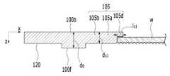
도1 및 도11은 본 발명의 바람직한 일 실시예에 따른 웨이퍼 크기 변환 장치의 후면을 도시한 도면이고, 도2 및 도12는 본 발명의 바람직한 일 실시예에 따른 웨이퍼 크기 변환 장치의 전면을 도시한 도면이다. 이들을 참조하면, 본 발명의 웨이퍼 크기 변환 장치(100)는 원형 고리형상을 이루는 본체(100a)를 가지며 본체(100a) 중앙에는 삽입할 웨이퍼가 안착되는 중앙홀(101)이 형성된다. 웨이퍼 크기 변환 장치(100)의 최외각 직경인 외경(Do)은 표준 웨이퍼 크기 중 어느 하나를 갖는다. 예를 들어 150mm(6 인치), 200mm(8인치), 300mm(12인치), 450mm(18인치) 중 어느 하나 일 수 있다. 중앙홀(101)에는 외경(Do)보다 작은 구경의 웨이퍼가 안착된다. 이를 위하여 웨이퍼 크기 변환 장치(100) 후면(100b)의 가장 안쪽 직경으로 정의되는 웨이퍼 크기 변환 장치의 내경(Di)도 표준 웨이퍼 크기 중 어느 하나를 가진다. 예를 들어 외경(Do)이 450mm인 경우 내경(Di)은 300mm 또는 200mm일 수 있다. 또는 외경(Do)이 300mm인 경우 내경(Di)은 200mm 또는 150mm일 수 있다. 또는 외경(Do)이 200mm인 경우 내경(Di)은 150mm 이거나 그보다 작을 수 있다. 내경(Di)은 안착되는 웨이퍼의 표준 사이즈보다는 약간 큰 것이 바람직하다. 이는 안착되는 웨이퍼가 소정의 유격을 가지고 착탈 가능하도록 하기 위함이다. FIGS. 1 and 11 are views showing a rear surface of a wafer size conversion apparatus according to a preferred embodiment of the present invention, and FIGS. 2 and 12 show a front view of a wafer size conversion apparatus according to a preferred embodiment of the present invention, Fig. Referring to these drawings, the wafer
웨이퍼 크기 변환 장치(100) 외주부(100o) 상의 일 지점, 즉 도1의 12시방향 상단에는 웨이퍼 얼라인을 위한 외측 얼라인부(102)가 형성된다. 외측 얼라인부(102)는 웨이퍼에서 통상적으로 사용되는 노치(notch)와 동일한 형상을 가질 수 있다. 또한, 도시되어 있지는 않으나 웨이퍼에서 통상적으로 사용되는 플랫존(flat zone)과 같은 형상으로 커팅된 형태를 가질 수도 있으며, 그 외 웨이퍼의 결정방향을 표시하는 목적으로 사용되는 여하한 형상의 표식이 될 수도 있다.An
웨이퍼 크기 변환 장치(100)의 내주부(100i) 상에도, 즉 도1의 12시 방향에 내측 얼라인부(103)가 형성된다. 내측 얼라인부(103)는 안착될 웨이퍼의 플랫존(flat zone)부분을 수용할 수 있도록 플랫존과 같은 형상으로 만들어진다. 또한, 웨이퍼의 노치(notch) 부분을 수용할 수 있도록 노치 형상을 따라 만들어 질 수도 있으며(도 9 참조), 그 외 웨이퍼의 결정 방향을 표시하는 목적으로 사용되는 여하한 형상을 수용하는 모양으로 만들어 질 수 있다.In the inner peripheral portion (100i) of the wafer
내주부(100i)의 둘레를 따라서는 안착되는 웨이퍼가 아래 방향, 도1상의 지면방향으로 이탈되지 않도록 웨이퍼의 둘레부를 받쳐주는 이탈 방지턱(104)이 구성된다. 웨이퍼는 반도체 소자가 형성되는 전면(front side)이 아래를 향하도록 놓이게 되며 반도체 소자가 형성되지 않는 후면(back side)이 위를 향하도록 놓이게 된다. 즉 이탈 방지턱(104)은 반도체 소자가 형성되는 웨이퍼의 전면 가장자리를 받치게 된다. 이하에서는 안착되는 웨이퍼의 면방향과 방향성이 일치되도록 웨이퍼 크기 변환 장치(100)의 도1에 도시된 면을 후면(100b), 도2에 도시된 면을 전면(100f)이라고 한다.
The inner periphery
이하에서는 도3 내지 도7을 참조하여 웨이퍼 크기 변환 장치(100)의 단면을 상세히 설명한다. 설명의 편의를 위하여 도3 내지 7에서는 웨이퍼가 안착된 상태를 가정하여 단면도로 표현하였다.Hereinafter, a cross section of the wafer
도3에 도시된 바와 같이 이탈 방지턱(104)은 웨이퍼 크기 변환 장치(100) 후면(100b)으로부터 소정의 깊이 d1을 가지며 내주부(100i)로부터 돌출되는 길이 l1을 가진다. 이탈 방지턱(104) 깊이 d1은 웨이퍼(W)의 두께(Wd)보다 큰 것이 바람직하다. 일반적으로 150mm 웨이퍼의 경우는 두께 0.625mm, 200mm 웨이퍼는 두께 0.725mm, 300mm 웨이퍼는 두께 0.775mm를 표준 두께로 가지므로 안착되는 웨이퍼 구경에 따라 그 표준 두께보다 큰 깊이 d1을 갖도록 형성된다. 이탈 방지턱(104)은 반도체 소자가 형성되는 웨이퍼의 전면과 접촉되기 때문에 에지(edge)부분만 지지할 수 있도록 그 길이 l1은 수 mm 이내로 짧게, 바람직하게는 0.3mm ~ 3mm 이하로 짧게 형성하는 것이 바람직하다.As shown in FIG. 3, the
도1 및 도4를 참조하면, 웨이퍼 크기 변환 장치(100) 내주부(100i)둘레를 따라 웨이퍼(W)의 측면을 지지하는 제1,2,3,4 웨이퍼 측면 지지부(111, 112, 113, 114)가 구성된다. 제1 웨이퍼 측면 지지부(111)는 헤드부(111a)와 헤드부(111a)로부터 연장되어 본체(100a)로 이어지는 연결부(111b)를 포함한다. 헤드부(111a)와 연결부(111b)는 원주방향을 따라 시계방향으로 연장되는 형태를 갖는다. 헤드부(111a)와 연결부(111b) 둘레에는 헤드부(111a) 끝단 바깥쪽에서 반경방향으로 연장된 후 다시 그에 수직한 방향으로 연장되는 이격공간(111c)이 형성된다. 연결부(111b)는 헤드부(111a)에 가까워지면서 폭이 좁아지는 형상을 갖는다. 헤드부(111a)는 반경방향으로 소정의 탄성을 가지면서 유동하는 것이 바람직하다. 이를 위해서 웨이퍼 크기 변환 장치(100)는 금속과 같이 탄성 변형되는 물질로 제작되는 것이 바람직하다. 웨이퍼(W)가 안착된 상태에서 헤드부(111a)의 내측 측면(111d)은 웨이퍼(W) 측면에 소정의 압력을 가하도록 접촉되는 것이 바람직하다. 이는 운반과정이나 공정진행 과정에서 웨이퍼(W)가 웨이퍼 크기 변환 장치(100) 내에서 유동되지 않고 견고하게 고정되어 있도록 하기 위함이다.1, and 4, first, second, third, and fourth wafer side supports 111, 112, and 113 for supporting the sides of the wafer W along the periphery of the
제1 웨이퍼 측면 지지부(111)와 X축 대칭인 위치에 제2 웨이퍼 측면 지지부(112)가 구성되고, Y축 대칭인 위치에 제3 웨이퍼 측면 지지부(113)가 구성되고, 원점 대칭인 위치에 제4 웨이퍼 측면 지지부(114)가 구성된다. 제2,3,4 웨이퍼 측면 지지부(112, 113, 114)의 형상은 제1 웨이퍼 측면지지부(111)와 동일한 바, 상세한 설명은 생략한다.The second wafer
제1,2,3,4 웨이퍼 측면 지지부(111, 112, 113, 114)는 방사상으로 동일한 각도, 즉 90°를 이루어 분포되는 것이 바람직하다. 이러한 구조하에서 안착되는 웨이퍼(W)는 각 웨이퍼 측면 지지부(111, 112, 113, 114)로부터 균일한 지지력으로 견고하게 고정된다. 도시되어 있지는 않으나 이러한 웨이퍼 측면 지지부는 필요에 따라 2개소, 3개소, 5개소, 6개소 또는 그 이상 형성하는 것도 가능하며, 각각의 경우 방사상으로 동일한 각도로 분포되도록 구성하는 것이 바람직하다.The first, second, third, and fourth wafer side supports 111, 112, 113, 114 are preferably distributed radially at the same angle, i.e., 90 degrees. The wafer W that is seated under such a structure is firmly fixed from the wafer
도1 및 도5을 참조하면 웨이퍼 크기 변환 장치(100) 내주부(100i)에는 또한 웨이퍼(W)가 후면(100b) 방향으로 이탈하지 않도록 잡아주는 제1클램핑부(105)가 구성된다. 제1클램핑부(105)는 반경방향으로 연장되는 헤드부(105a)와 헤드부(105a)로부터 연장되어 웨이퍼 크기 변환 장치(100)의 본체(100a)로 연결되는 연결부(105b)를 갖는다. 연결부(105b)는 본체(100a)에서 헤드부(105a)로 갈수록 폭이 좁아지는 형상을 갖는다. 헤드부(105a)와 연결부(105b) 주위에는 본체(100a)방향으로 만입되는 홈부(105c)가 형성된다. 도5에 도시된 바와 같이 헤드부(105a) 앞단에는 웨이퍼(W)의 후면 모서리를 잡아주는 턱부(105d)가 형성된다. 턱부(105d) 길이 lc1은 웨이퍼(W) 후면 모서리에 약간 중첩되는 정도, 바람직하게는 2mm이내의 길이를 갖는다. 제1클램핑부(105)의 두께 dc1은 본체(100a) 두께 db보다 작도록 씨닝(thinning)되어 있다. 이는 턱부(105d)를 포함하는 제1클램핑부(105) 선단부가 전후방 즉 Z축 방향으로 탄성 변형되기 용이하도록 하기 위함이다.Referring to FIGS. 1 and 5, a
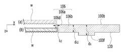
도1 및 도6을 참조하면, 제1클램핑부(105)의 반대편에도 웨이퍼(W)가 후면(100b) 방향으로 이탈하지 않도록 잡아주는 제2클램핑부(106)가 구성된다. 즉 안착된 웨이퍼(W)는 제1,2클램핑부(105, 106)에 의해 그 후면 양측 모서리가 지지된다. 제1클램핑부(105)와 마찬가지로 제2클램핑부(106)도 헤드부(106a)와 연결부(106b)를 가지며, 그 주위로 홈부(106c)가 형성된다. 한편, 턱부(106d)는 길이 lc2가 제1클램핑부(105)의 턱부(105d) 길이 lc1보다 작으며, 그1/2 또는 그 이하인 것이 바람직하다. 이는 웨이퍼(W)를 삽입할 때 웨이퍼 일측단부를 제1클램핑부(105)아래 먼저 끼워 넣은 후 반대편 단부는 그후에 제2클램핑부(106)측에 끼워 넣도록 예정한 것이다. 조금 더 상세히 설명하면 웨이퍼(W)를 웨이퍼 크기 변환 장치(100)에 안착시키기 위해 사용자는 우선 웨이퍼(W)를 제1클램핑부(105)쪽에 먼저 끼워 넣으면 제1,2 웨이퍼 측면 지지부(111, 112)가 바깥쪽으로 탄성변형되어 밀리면서 웨이퍼(W)는 정위치보다는 X축 방향으로 약간 유동된 상태로 도6의 (a)와 같이 위치된다. 그 후 다시 반대편을 제2클램핑부(106)에 끼워 넣으면 제1,2 웨이퍼 측면 지지부(111, 112)가 다시 웨이퍼(W)를 안쪽으로 밀어주면서 정위치에 위치시키고 웨이퍼(W)는 도6의 (b)위치에 오게 된다. 웨이퍼 크기 변환 장치(100) 후면(100b)에는 웨이퍼를 끼워 넣는 방향을 표시하는 화살표 모양의 마킹(M)이 제1클램핑부(105) 옆에 표기되어 있다. 마킹(M)은 후면(100b)상에 덴트(Dent)로 형성되는 것이 바람직하다. 도시된 화살표 형상 이외에도 문자나 다른 다양한 기호가 이용될 수도 있다.Referring to FIGS. 1 and 6, a
제2클램핑부(106)의 두께 dc2도 본체(100a) 두께 db보다 작도록 씨닝(thinning)되어 있다. dc2는 dc1과 같거나 혹은 다를 수 있다. 제2클램핑부(106)의 선단부가 Z축 방향으로 탄성 변형이 용이하도록 하기 위해서는 dc2를 dc1보다 작게 만드는 것이 바람직하다.The thickness dc2 of the
도1 및 도7를 참조하면, 본체(100a)의 후면(100b) 상에는 장비 내에서 웨이퍼를 이송하는 로봇암(500)이 인입될 수 있도록 안내하는 로봇암 가이드(107)가 구성된다. 로봇암 가이드(107)는 양단이 Y축 방향을 따라 평행한 방향으로 후면(100b)상에 단차 형태로 형성된다. 로봇암(500)은 로봇암 가이드(107)를 따라 반경방향으로 이동하며 웨이퍼 후면을 지지하여 장비 내에서 웨이퍼를 이송한다.Referring to FIGS. 1 and 7, a
도2 및 도12를 참조하면 웨이퍼 크기 변환 장치(100) 전면(100f) 둘레에는 “C”자 형상의 씨닝부(120)가 형성된다. 씨닝부(120)는 상술한 로봇암 가이드(107)의 이면에는 형성되어 있지 않다. 씨닝부(120)는 웨이퍼 크기 변환 장치(100)의 전체적인 무게를 줄이면서 원형 둘레 전체에 걸쳐 무게의 밸런스를 맞추기 위한 것으로 필요에 따라 그 두께나 길이를 조절하는 것이 바람직하다.Referring to FIGS. 2 and 12, a C-shaped
도8은 본 발명의 웨이퍼 크기 변환 장치(100)와 함께 사용하는 고정 지그(200)를 도시한 사시도이다. 고정지그(200)는 전체적으로 사각판 형상을 갖는다. 그 윗면에는 웨이퍼 크기 변환 장치(100)의 외경(Do)와 같은 직경을 갖는 안착홈(201)이 형성되고, 안착홈 안쪽으로 웨이퍼 크기 변환 장치(100)와 같은 링형상으로 이루어진 받침부(202)가 구성된다. 받침부(202)에는 웨이퍼 크기 변환 장치(100)의 위치를 고정시키기 위한 제1,2,3 돌기(202a, 202b, 202c)가 형성된다. 제1,2,3 돌기(202a, 202b, 202c)는 받침부(202) 상부로 돌출되도록 형성되며, 방사상으로 동일한 각도를 이루도록 위치시키는 것이 바람직하다. 웨이퍼 크기 변환 장치(100)에는 이들 제1,2,3 돌기(202a, 202b, 202c)에 끼워 맞춰지는 제1,2,3고정홀(108a, 108b, 108c)이 천공되어 있다.8 is a perspective view showing a fixing
이하에서는 본 발명의 웨이퍼 크기 변환 장치(100)에 웨이퍼를 장착하는 방법을 상세히 설명한다. 반도체 설비에서 작업하는 오퍼레이터는 우선 고정지그(200)에 웨이퍼 크기 변환 장치(100)의 전면(100f)이 고정지그(200)를 향하도록 한 상태에서 제1,2,3 고정홀(108a, 108b, 108c)과 제1,2,3 돌기(202a, 202b, 202c)가 각각 맞춰지도록 웨이퍼 크기 변환 장치(100)를 끼워 넣는다. 그 후 준비한 소구경의 웨이퍼를 가공면인 전면을 고정지그(200) 쪽으로 향하게 하여 제1클램핑부(105)쪽에 먼저 끼워 넣고 이 상태에서 반대쪽을 제2클램핑부(160) 아래쪽으로 밀어 넣는다. 웨이퍼는 소정의 유격(수 mm이내)을 갖고 유동하면서 제1,2,3,4 웨이퍼 측면 지지부(111,112,113,114)에 측면이 지지되면서 이탈 방지턱(104) 및 제1,2 클램핑부(105, 106)에 의해 고정된다. 웨이퍼는 가공면인 전면이 고정 지그(200) 쪽을 향하기 때문에 가공면이 고정지그(200)와 직접 닿지 않도록 받침부(202)의 안쪽은 아래로 오목하게 단차를 갖는다. 한편, 오퍼레이터가 웨이퍼 크기 변환 장치(100)를 고정지그(200)에 넣고 빼기 쉽도록 고정지그(200) 좌우에는 손잡이홈(203)이 형성된다.Hereinafter, a method of mounting a wafer on the wafer
웨이퍼가 웨이퍼 크기 변환 장치(100)에 고정된 상태로 다음 공정을 위한 준비가 완료되면 오퍼레이터는 진공 트위저(tweezer)등을 이용해 고정지그(200) 위를 향하고 있는 웨이퍼 후면을 잡아 웨이퍼 카세트에 적재하여 다음 공정을 진행 시킨다.When the wafer is fixed to the wafer
도9는 본 발명의 다른 일 실시예에 따른 웨이퍼 크기 변환 장치(300)를 도시한 것으로 내측 얼라인부(303)가 노치(notch) 타입인 것을 제외하고는 상술한 실시예에 따른 웨이퍼 크기 변환 장치(100)와 동일한 구성을 갖는다. 도9의 실시예에 따른 웨이퍼 크기 변환 장치(300)는 예를 들어, 노치타입 200mm 웨이퍼를 노치타입 300mm 웨이퍼 설비에서 공정을 진행시키기 위한 용도로 사용될 수 있다.9 shows a wafer
도10은 본 발명의 또 다른 일 실시예에 따른 웨이퍼 크기 변환 장치(400)를 도시한 것으로 외측 얼라인부(402)와 내측 얼라인부(403)가 일정한 각도, 예를 들어 45°나 90°등의 각도를 이루고 있는 점을 제외하고는 도1의 실시예에 따른 웨이퍼 크기 변환 장치(100)와 동일한 구성을 갖는다. 반도체 소자는 결정 방향에 따라 저항, 캐패시턴스, 임계 전압(Vth)등의 전기적 특성을 서로 달리하는데, 이러한 특성 변화를 이용하고자 하는 경우 본 실시예에 따른 웨이퍼 크기 변환 장치(400)를 이용 할 수 있다.10 illustrates a wafer
이상의 실시예를 통해 설명한 본 발명에 따른 웨이퍼 크기 변환 장치는 소구경의 웨이퍼를 그 보다 큰 대구경 웨이퍼 설비를 이용해 공정을 진행하는 것을 가능하게 하여 설비 운영을 효율화 할 수 있게 해주는 장점이 있다. 한편, 소구경 웨이퍼를 장착한 웨이퍼 크기 변환장치를 대구경 웨이퍼 설비에서 오류 없이 공정진행 할 수 있도록 하기 위해서는 웨이퍼 크기 변환장치의 외경 크기 뿐만 아니라 그 무게도 대구경 웨이퍼에 맞추는 것이 필요하다. 즉 소구경 웨이퍼와 웨이퍼 크기 변환 장치의 무게 합이 대구경 웨이퍼와 같거나 또는 대구경 웨이퍼 설비가 오류 없이 공정을 진행 할 수 있을 정도의 무게이어야 한다. 이는 설비마다 다를 수 있으나 바람직하게는 대구경 웨이퍼 무게의 60% ~ 150% 범위인 것이 바람직하다.The wafer size conversion apparatus according to the present invention described above has the advantage of enabling efficient operation of the facility by making it possible to process the small diameter wafers using the larger diameter wafer facility. On the other hand, in order to enable the wafer size conversion apparatus equipped with small diameter wafers to be processed without errors in the large-diameter wafer facility, it is necessary to match not only the outer diameter size of the wafer size conversion apparatus but also its weight to the large diameter wafers. That is, the sum of the small diameter wafers and the wafer size conversion apparatus should be the same as that of the large diameter wafers, or the weight of the large diameter wafers should be such that the wafers can be processed without errors. This may vary from equipment to equipment, but is preferably in the range of 60% to 150% of the weight of the large diameter wafer.
또한, 본 발명에 따른 웨이퍼 크기 변환 장치는 대구경 웨이퍼 설비에서 오류 없이 공정을 진행 할 수 있는 소재로 만드는 것이 바람직하다. 즉 공정 챔버 내에서 파티클을 유발하거나 오염 가스를 일으키지 않는 소재 예를 들면 세라믹과 같은 소재로 만들거나 또는 알루미늄 소재로 만드는 것이 바람직하다. 특히 선폭 측정 장비(CD-SEM, Critical Dimension Scanning Electron Microscope)와 같은 측정 장비에서는 전자빔에 따른 변형을 일으키지 않는 알루미늄 소재로 만든 것을 사용하는 것이 바람직하다.In addition, it is preferable that the wafer size conversion apparatus according to the present invention be made of a material capable of proceeding with no errors in a large-diameter wafer facility. That is, it is preferable to make a material such as ceramics or an aluminum material that does not cause particles or cause pollution gas in the process chamber. In particular, in a measuring instrument such as a CD-SEM (Critical Dimension Scanning Electron Microscope), it is preferable to use an aluminum material which does not cause deformation due to an electron beam.
이상의 실시예들에서 웨이퍼는 반도체 소자가 형성되는 가공면인 전면이 웨이퍼 크기 변환장치의 전면을 향하도록 설치되는 것으로 설명하였으나, 필요에 따라서는 반대로, 즉 웨이퍼 전면이 웨이퍼 크기 변환장치의 후면을 향하도록 설치될 수도 있으며, 이는 공정설비의 필요에 따라 변형되어 사용될 수 있다.In the above embodiments, the front surface of the wafer, on which the semiconductor elements are formed, is set to face the front surface of the wafer size conversion apparatus. However, if necessary, conversely, the front surface of the wafer is directed to the rear surface of the wafer size conversion apparatus , Which may be modified and used according to the needs of the process facility.
이러한 본 발명에 따른 웨이퍼 크기 변환 장치를 이용하면, 소구경 웨이퍼를 그보다 큰 대구경 웨이퍼 처럼 처리할 수 있도록 변형해 줌으로써, 대구경 웨이퍼 설비의 개조나 변경이 없이도 하나의 설비로 대구경 웨이퍼와 소구경 웨이퍼를 함께 처리하는 것이 가능해진다. 따라서 설비의 활용도와 호환성을 높여주고 설비 투자 비용을 절감할 수 있는 효과가 있다.By using the wafer size conversion apparatus according to the present invention, a small-diameter wafer can be processed like a large-diameter wafer larger than the large-diameter wafer, so that a large-diameter wafer and a small- It becomes possible to process them together. Therefore, it is possible to increase the compatibility with the utility of the facility and reduce the investment cost of the facility.
100, 300, 400 : 웨이퍼 크기 변환 장치
101 : 중앙홀
102 : 외측 얼라인부
103 : 내측 얼라인부
104 : 이탈 방지턱
105, 106 : 클램핑부
107 : 로봇암 가이드
111, 112, 113, 114 : 웨이퍼 측면 지지부
120 : 씨닝부
200 : 고정 지그100, 300, 400: wafer size converter
101: center hole
102: outer aligning portion
103: Inner-
104:
105 and 106:
107: Robot arm guide
111, 112, 113, 114: wafer side support
120:
200: Fixing jig
Claims (7)
Translated fromKorean상기 제1구경보다 큰 제2구경을 갖는 외주부와,
상기 내주부에 형성되며 그에 안착되는 웨이퍼와 방향성을 일치시키기 위한 내측 얼라인부와,
상기 외주부에 형성되어 방향성을 표시하는 외측 얼라인부와,
상기 내주부 상에 형성되며 안착되는 웨이퍼의 측면을 지지하는 측면지지부와,
상기 안착되는 웨이퍼의 전후방향 이탈을 방지하기 위한 이탈방지부를 포함하고,
상기 이탈방지부는 상기 내주부를 따라 돌출되어 안착되는 웨이퍼의 일면 모서리를 지지하는 이탈 방지턱과, 상기 내주부에서 돌출되도록 형성되며 상기 안착되는 웨이퍼의 반대면 모서리를 지지하는 클램핑부를 포함하는 웨이퍼 크기 변환 장치.An inner peripheral portion forming a central hole to which the wafer of the first diameter is to be seated,
An outer peripheral portion having a second bore diameter larger than the first bore diameter,
An inner aligning portion formed on the inner circumferential portion and adapted to align the direction with the wafer placed on the inner circumferential portion,
An outer aligning portion formed on the outer circumferential portion and indicating a direction,
A side support portion formed on the inner peripheral portion and supporting a side surface of the wafer to be seated;
And a separation preventing portion for preventing the wafer to be seated from being displaced in the longitudinal direction,
And a clamping unit configured to protrude from the inner circumferential portion and to support an opposite surface edge of the wafer to be seated, wherein the detachment preventing portion includes a separation preventing projection for supporting one side edge of the wafer protruded and seated along the inner circumference, Device.
상기 클램핑부는 상기 안착되는 웨이퍼 반대면 모서리를 지지하도록 제1길이 만큼 돌출되는 턱부를 갖는 제1클램핑부와,
상기 내주부 상에 상기 제1클램핑부의 반대편에 형성되며, 상기 제1길이보다 작은 제2길이 만큼 돌출되는 턱부를 갖는 제2클램핑부를 포함하는 웨이퍼 크기 변환 장치.The method according to claim 1,
Wherein the clamping portion includes a first clamping portion having a protruding portion protruding by a first length so as to support the opposite face edge of the wafer to be seated,
And a second clamping portion formed on the inner circumference portion opposite to the first clamping portion and having a protruding portion protruding by a second length smaller than the first length.
상기 웨이퍼 크기 변환 장치는 상기 웨이퍼 크기 변환 장치의 후면에 형성되며 공정설비의 로봇암의 인입 경로를 안내하도록 단차지게 형성된 로봇암 가이드를 더 포함하는 웨이퍼 크기 변환 장치.The method according to claim 1,
Wherein the wafer size conversion device further comprises a robot arm guide formed on the back surface of the wafer size conversion device and formed to be stepped to guide the pulling path of the robot arm of the process facility.
상기 웨이퍼 크기 변환 장치는 상기 웨이퍼 크기 변환 장치의 후면에 형성되며 상기 안착되는 웨이퍼의 삽입 방향을 안내하는 마킹을 더 포함하는 웨이퍼 크기 변환 장치.The method according to claim 1,
Wherein the wafer size conversion device further comprises marking formed on a rear surface of the wafer size conversion device and guiding an insertion direction of the loaded wafer.
상기 외측 얼라인부는 노치 타입으로 형성되며,
상기 내측 얼라인부는 플랫존 타입으로 형성되는 웨이퍼 크기 변환 장치.The method according to claim 1,
Wherein the outer alignment portion is formed in a notch type,
Wherein the inner alignment portion is formed in a flat zone type.
Priority Applications (1)
| Application Number | Priority Date | Filing Date | Title |
|---|---|---|---|
| KR1020150004406AKR101590310B1 (en) | 2015-01-12 | 2015-01-12 | A Wafer Size Conversion Tool |
Applications Claiming Priority (1)
| Application Number | Priority Date | Filing Date | Title |
|---|---|---|---|
| KR1020150004406AKR101590310B1 (en) | 2015-01-12 | 2015-01-12 | A Wafer Size Conversion Tool |
Publications (1)
| Publication Number | Publication Date |
|---|---|
| KR101590310B1true KR101590310B1 (en) | 2016-02-01 |
Family
ID=55354179
Family Applications (1)
| Application Number | Title | Priority Date | Filing Date |
|---|---|---|---|
| KR1020150004406AActiveKR101590310B1 (en) | 2015-01-12 | 2015-01-12 | A Wafer Size Conversion Tool |
Country Status (1)
| Country | Link |
|---|---|
| KR (1) | KR101590310B1 (en) |
Cited By (3)
| Publication number | Priority date | Publication date | Assignee | Title |
|---|---|---|---|---|
| CN114038789A (en)* | 2021-11-29 | 2022-02-11 | 莱腾仕精密机电(上海)有限公司 | Multi-size wafer fast switching module |
| CN114242569A (en)* | 2021-12-14 | 2022-03-25 | 长春长光圆辰微电子技术有限公司 | Method for processing flat-edge wafer by notch-shaped wafer processing equipment |
| CN115020301A (en)* | 2022-06-28 | 2022-09-06 | 乂易半导体科技(无锡)有限公司 | Method for applying small-size wafer to large-size wafer etching equipment |
Citations (3)
| Publication number | Priority date | Publication date | Assignee | Title |
|---|---|---|---|---|
| KR980012164A (en)* | 1996-07-04 | 1998-04-30 | 김광호 | Wafer socket for semiconductor equipment compatibility test |
| KR200205789Y1 (en)* | 2000-07-12 | 2000-12-01 | 주식회사햇님토이 | Scooter for a children |
| JP2010258288A (en)* | 2009-04-27 | 2010-11-11 | Sanyo Electric Co Ltd | Fixing jig and semiconductor device manufacturing method using the same |
- 2015
- 2015-01-12KRKR1020150004406Apatent/KR101590310B1/enactiveActive
Patent Citations (3)
| Publication number | Priority date | Publication date | Assignee | Title |
|---|---|---|---|---|
| KR980012164A (en)* | 1996-07-04 | 1998-04-30 | 김광호 | Wafer socket for semiconductor equipment compatibility test |
| KR200205789Y1 (en)* | 2000-07-12 | 2000-12-01 | 주식회사햇님토이 | Scooter for a children |
| JP2010258288A (en)* | 2009-04-27 | 2010-11-11 | Sanyo Electric Co Ltd | Fixing jig and semiconductor device manufacturing method using the same |
Cited By (4)
| Publication number | Priority date | Publication date | Assignee | Title |
|---|---|---|---|---|
| CN114038789A (en)* | 2021-11-29 | 2022-02-11 | 莱腾仕精密机电(上海)有限公司 | Multi-size wafer fast switching module |
| CN114242569A (en)* | 2021-12-14 | 2022-03-25 | 长春长光圆辰微电子技术有限公司 | Method for processing flat-edge wafer by notch-shaped wafer processing equipment |
| CN115020301A (en)* | 2022-06-28 | 2022-09-06 | 乂易半导体科技(无锡)有限公司 | Method for applying small-size wafer to large-size wafer etching equipment |
| CN115020301B (en)* | 2022-06-28 | 2024-05-24 | 乂易半导体科技(无锡)有限公司 | Method for applying small-size wafer to large-size wafer etching equipment |
Similar Documents
| Publication | Publication Date | Title |
|---|---|---|
| TWI739093B (en) | Wireless substrate-like teaching sensor for semiconductor processing | |
| US7652467B2 (en) | Carrier tray for use with prober | |
| KR101590310B1 (en) | A Wafer Size Conversion Tool | |
| US9966292B2 (en) | Centering fixture for electrostatic chuck system | |
| US20250232997A1 (en) | Adaptive positioning systems and routines using an autocalibration wafer and a calibration wafer with cutouts | |
| TWI300845B (en) | Method and apparatus for manufacturing a probe card | |
| JP5390486B2 (en) | Electronic component post-processing system | |
| JP2018507791A (en) | Clamping system that can be automated | |
| US11806794B2 (en) | Processing device and processing method | |
| IL104267A (en) | Apparatus for providing consistent registration of semiconductor wafers | |
| US6460436B1 (en) | Reversible micromachining locator | |
| KR20040062685A (en) | Method and apparatus for alignment of carriers, carrier handlers and semiconductor handling equipment | |
| KR20160022732A (en) | Jig and Method for Assembling Wafer Tray | |
| US12074400B1 (en) | Substrate dimension adapter | |
| CN205733993U (en) | A positioning tooling device | |
| CN210272297U (en) | Wafer auxiliary guiding equipment | |
| CN209533182U (en) | A precision positioning fixture | |
| KR102651197B1 (en) | Smart origin position setting device for electric discharge machine | |
| CN205373573U (en) | A subassembly is examined to knuckle high efficiency | |
| CN220912329U (en) | Bearing device and measuring equipment | |
| CN223347752U (en) | Carrier tool | |
| CN222520562U (en) | Chuck correction jig and workpiece fixing device | |
| JP4578315B2 (en) | Wafer positioning jig, wafer fixing stand, and wafer analysis method | |
| US20250153292A1 (en) | Vacuum chuck for high warpage wafers | |
| US20070107181A1 (en) | Datum transfer method and apparatus |
Legal Events
| Date | Code | Title | Description |
|---|---|---|---|
| PA0109 | Patent application | Patent event code:PA01091R01D Comment text:Patent Application Patent event date:20150112 | |
| PA0201 | Request for examination | ||
| PE0902 | Notice of grounds for rejection | Comment text:Notification of reason for refusal Patent event date:20151012 Patent event code:PE09021S01D | |
| E90F | Notification of reason for final refusal | ||
| PE0902 | Notice of grounds for rejection | Comment text:Final Notice of Reason for Refusal Patent event date:20160104 Patent event code:PE09021S02D | |
| E701 | Decision to grant or registration of patent right | ||
| PE0701 | Decision of registration | Patent event code:PE07011S01D Comment text:Decision to Grant Registration Patent event date:20160108 | |
| GRNT | Written decision to grant | ||
| PR0701 | Registration of establishment | Comment text:Registration of Establishment Patent event date:20160126 Patent event code:PR07011E01D | |
| PR1002 | Payment of registration fee | Payment date:20160126 End annual number:3 Start annual number:1 | |
| PG1601 | Publication of registration | ||
| FPAY | Annual fee payment | Payment date:20190108 Year of fee payment:4 | |
| PR1001 | Payment of annual fee | Payment date:20190108 Start annual number:4 End annual number:4 | |
| FPAY | Annual fee payment | Payment date:20200111 Year of fee payment:5 | |
| PR1001 | Payment of annual fee | Payment date:20200111 Start annual number:5 End annual number:5 | |
| PR1001 | Payment of annual fee | Payment date:20210106 Start annual number:6 End annual number:6 | |
| PR1001 | Payment of annual fee | Payment date:20211201 Start annual number:7 End annual number:7 | |
| PR1001 | Payment of annual fee | Payment date:20221130 Start annual number:8 End annual number:8 | |
| PR1001 | Payment of annual fee | Payment date:20231220 Start annual number:9 End annual number:9 | |
| PR1001 | Payment of annual fee | Payment date:20250319 Start annual number:10 End annual number:10 |