KR101590148B1 - Light emitting device and method for manufacturing light emitting element - Google Patents
Light emitting device and method for manufacturing light emitting elementDownload PDFInfo
- Publication number
- KR101590148B1 KR101590148B1KR1020117030615AKR20117030615AKR101590148B1KR 101590148 B1KR101590148 B1KR 101590148B1KR 1020117030615 AKR1020117030615 AKR 1020117030615AKR 20117030615 AKR20117030615 AKR 20117030615AKR 101590148 B1KR101590148 B1KR 101590148B1
- Authority
- KR
- South Korea
- Prior art keywords
- light emitting
- layer
- electrode
- emitting device
- emitting element
- Prior art date
- Legal status (The legal status is an assumption and is not a legal conclusion. Google has not performed a legal analysis and makes no representation as to the accuracy of the status listed.)
- Expired - Fee Related
Links
Images


Classifications
- H—ELECTRICITY
- H10—SEMICONDUCTOR DEVICES; ELECTRIC SOLID-STATE DEVICES NOT OTHERWISE PROVIDED FOR
- H10K—ORGANIC ELECTRIC SOLID-STATE DEVICES
- H10K50/00—Organic light-emitting devices
- H10K50/10—OLEDs or polymer light-emitting diodes [PLED]
- H10K50/14—Carrier transporting layers
- H—ELECTRICITY
- H10—SEMICONDUCTOR DEVICES; ELECTRIC SOLID-STATE DEVICES NOT OTHERWISE PROVIDED FOR
- H10K—ORGANIC ELECTRIC SOLID-STATE DEVICES
- H10K50/00—Organic light-emitting devices
- H10K50/10—OLEDs or polymer light-emitting diodes [PLED]
- H10K50/17—Carrier injection layers
Landscapes
- Physics & Mathematics (AREA)
- Optics & Photonics (AREA)
- Electroluminescent Light Sources (AREA)
Abstract
Translated fromKoreanDescription
Translated fromKorean본 발명은, 한 쌍의 전극 사이에 복수의 층이 놓이는 구조를 갖도록 형성된 발광 소자에 관한 것으로서, 특히, 본 발명은 복수의 층 내의 적어도 한 층으로서 사용될 수 있는 복합재료를 포함하는 층 구조에 관한 것이다.The present invention relates to a light emitting device formed so as to have a structure in which a plurality of layers are arranged between a pair of electrodes, and in particular, the present invention relates to a layer structure including a composite material which can be used as at least one layer in a plurality of layers will be.
전자발광 소자(electroluminescent element)(발광 소자)로부터의 발광을 이용하는 발광 장치는 디스플레이 장치 또는 조명 장치로서 주목을 받아왔다.BACKGROUND ART A light emitting device using light emission from an electroluminescent element (light emitting element) has attracted attention as a display device or a lighting device.
발광 장치에 사용되는 발광 소자로서, 한 쌍의 전극 사이에 삽입되는 발광 화합물을 포함하는 층을 포함한 발광 소자가 잘 알려져 있다.As a light emitting element used in a light emitting device, a light emitting element including a layer containing a light emitting compound inserted between a pair of electrodes is well known.
전극 중 어느 하나가 애노드 역할을 하고, 다른 전극이 캐소드 역할을 하는 상기 발광 소자내에서, 애노드로부터 주입된 정공과 캐소드로부터 주입된 전자가 서로 재결합되어 분자 엑시톤(molecular exciton)을 형성하고, 분자 엑시톤이 접지 상태로 복귀하면서 에너지를 빛으로 방출한다.Holes injected from the anode and electrons injected from the cathode are recombined with each other to form molecular excitons in the light emitting element in which one of the electrodes serves as an anode and the other electrode serves as a cathode, Returning to the ground state and emitting energy into light.
최근 급격하게 개발되고 있는 다양한 정보 처리 장치에 설치될 디스플레이 장치에서는 낮은 전력 소비에 대한 요구가 특히 증가한다. 낮은 전력 소비를 이루기 위해, 발광 소자를 구동하는 전압을 감소시키려는 시도가 이루어졌다. 상업화를 고려하면, 발광 소자를 구동하는 전압을 감소시키는 것뿐 아니라, 발광 장치의 수명을 연장하는 것이 중요하다. 따라서, 발광 장치는 낮은 전력 소비 및 긴 수명을 얻도록 개발되어 왔다.A demand for low power consumption is particularly increased in a display device to be installed in various information processing apparatuses which have been rapidly developed recently. In order to achieve low power consumption, attempts have been made to reduce the voltage driving the light emitting element. In consideration of commercialization, it is important not only to reduce the voltage driving the light emitting element but also to extend the lifetime of the light emitting device. Thus, light emitting devices have been developed to achieve low power consumption and long life.
예컨대, 공개 특허 공보 No.9-63771호에는, 발광 소자를 구동하는 전압이 몰리브덴 산화물과 같은 큰 일함수를 가진 금속 산화물을 이용하여 애노드를 형성함으로써 감소된다는 것이 개시되어 있다. 또한, 발광 소자의 수명이 연장될 수 있다.For example, in Japanese Laid-Open Patent Publication No. 9-63771, it is disclosed that a voltage for driving a light emitting element is reduced by forming an anode using a metal oxide having a large work function such as molybdenum oxide. Further, the lifetime of the light emitting element can be extended.
상기 공개 특허 공보 No.9-63771에 개시되어 있는 발광 소자의 수명을 연장하는 수단은 불충분하여, 더 긴 수명을 얻기 위한 기술을 개발할 필요가 있다.
The means for prolonging the lifetime of the light-emitting device disclosed in the above-mentioned JP-A-9-63771 is insufficient, and it is necessary to develop a technique for obtaining a longer lifetime.
본 발명의 목적은 통상적인 발광 소자보다 더 긴 수명을 가지며 낮은 전압에서 구동하는 발광 장치 및 발광소자의 제조 방법과, 발광 소자의 제조에 사용되는 복합재료 및 그 제조방법을 제공하는 것이다.
It is an object of the present invention to provide a light emitting device and a method of manufacturing a light emitting device which have a longer lifetime than a conventional light emitting device and are driven at a low voltage, a composite material used for manufacturing the light emitting device, and a manufacturing method thereof.
본 발명의 일 관점에 따르면, 발광 소자는 한 쌍의 전극 사이에 복수의 층을 포함하며, 상기 복수의 층 중에서 적어도 한 층은 산화물 반도체와 금속 산화물로 구성된 그룹에서 선택되는 무기 화합물, 및 높은 정공 수송 특성을 가진 유기 화합물을 포함하는 하이브리드 재료(hybrid material)(복합 재료)를 포함한다.According to one aspect of the present invention, a light emitting device includes a plurality of layers between a pair of electrodes, and at least one of the plurality of layers includes an inorganic compound selected from the group consisting of an oxide semiconductor and a metal oxide, And a hybrid material (composite material) containing an organic compound having transport characteristics.
복수의 층은 높은 캐리어 주입 특성을 가진 물질, 높은 캐리어 수송 특성을 가진 물질 등에 의해 각각 형성된 층으로 구성되어, 발광 영역이 전극으로부터 떨어져 놓인다.The plurality of layers is composed of a layer each formed of a material having a high carrier injection property, a material having a high carrier transporting property, and the like, so that the light emitting region is separated from the electrode.
이러한 발광 소자는 산화물 반도체와 금속 산화물로 구성된 그룹에서 선택되는 한 화합물, 및 높은 정공 수송 특성을 가진 화합물을 포함하는 층의 결정화를 억제할 수 있다. 그 결과, 발광 소자의 수명이 연장될 수 있다.Such a light emitting element can suppress the crystallization of a compound selected from the group consisting of an oxide semiconductor and a metal oxide, and a layer including a compound having a high hole transporting property. As a result, the lifetime of the light emitting element can be prolonged.
산화물 반도체 및 금속 산화물에 대한 소정의 예로서는, 본원에 인용된 물질들로 제한되지 않지만, 몰리브덴 산화물(MoOx), 바나듐 산화물(VOx), 루테늄 산화물(RuOx), 텅스텐 산화물(WOx) 등이 사용될 수 있다. 이 외에도, 인듐 주석 산화물(ITO), 아연 산화물(ZnO), 및 주석 산화물(SnO)이 사용될 수 있다. 상기 물질 이외의 다른 물질이 사용될 수 있다.Specific examples of oxide semiconductors and metal oxides may include molybdenum oxide (MoOx), vanadium oxide (VOx), ruthenium oxide (RuOx), tungsten oxide (WOx), and the like, . In addition, indium tin oxide (ITO), zinc oxide (ZnO), and tin oxide (SnO) may be used. Materials other than the above materials may be used.
높은 정공 수송 특성을 가진 화합물로는, 본원에 인용된 물질들로 제한되지 않지만, 4,4'-비스[N-(1-나프틸)-N-페닐-아미노]-바이페닐(4,4'-bis[N-(1-naphtyl)-N-phenyl-amino]-biphenyl )(약어 α-NPD), 4,4'-비스[N-(3-메틸페닐)-N-페닐-아미노]-바이페닐(4,4'-bis[N-(3-methylphenyl)-N-phenyl-amino]-biphenyl )(약어 TPD), 4,4',4"-트리스(N,N-디페닐-아미노)-트리페닐아민(4,4',4"-tris(N,N-diphenyl-amino)-triphenylamine )(약어 TDATA), 4,4',4"-트리스[N-(3-메틸페닐)-N-페닐-아미노]-트리페닐아민(4,4',4"-tris[N-(3-methylphenyl)-N-phenyl-amino]-triphenylamine)(약어 MTDATA)와 같은 방향족 화합물(즉, 벤젠 고리와 질소의 결합을 가진 화합물)이 사용될 수 있다. 상기 물질 이외의 다른 물질이 사용될 수 있다.Compounds with high hole transport properties include, but are not limited to, the 4,4'-bis [N- (1-naphthyl) -N-phenyl-amino] -biphenyl N-phenyl-amino] -biphenyl (abbrev.? -NPD), 4,4'-bis [N- (1-naphthyl) Biphenyl (abbreviated as TPD), 4,4 ', 4 "-tris (N, N-diphenyl-amino ) - triphenylamine (TDATA), 4,4 ', 4 "-tris [N- (3-methylphenyl) Aromatic compounds such as benzene (e.g., benzene) such as N, N-phenyl-amino] -triphenylamine (abbreviated as MTDATA) A compound having a bond of a ring and nitrogen) may be used. Materials other than the above materials may be used.
본 발명의 일 관점에 따르면, 발광 소자는 한 쌍의 전극 사이에 복수의 층을 포함하며, 상기 복수의 층 중에서 적어도 한 층은, 산화물 반도체와 금속 산화물로 구성된 그룹에서 선택되는 하나의 화합물, 높은 정공 수송 특성을 가진 화합물, 및 높은 입체 장애를 가진 화합물을 포함한다.According to one aspect of the present invention, a light emitting device includes a plurality of layers between a pair of electrodes, and at least one of the plurality of layers is a compound selected from the group consisting of an oxide semiconductor and a metal oxide, Compounds having hole transporting properties, and compounds having high steric hindrance.
상기 언급된 발광 소자와 동일하게, 복수의 층은 높은 캐리어 주입 특성을 가진 물질, 높은 캐리어 수송 특성을 가진 물질 등에 의해 각각 형성된 층으로 구성되어, 발광 영역이 전극으로부터 떨어져 놓인다.Like the above-mentioned light emitting device, the plurality of layers is composed of a layer each formed of a material having a high carrier injection property, a material having a high carrier transporting property, and the like, and the light emitting area is separated from the electrode.
산화물 반도체와 금속 산화물로 구성된 그룹에서 선택되는 하나의 화합물, 높은 정공 수송 특성을 가진 화합물, 및 높은 입체 장애를 가진 화합물을 포함한 층을 포함하는 발광 소자는 층의 결정화를 억제할 수 있다. 그 결과, 발광 소자의 수명이 연장될 수 있다.A light emitting device comprising a compound selected from the group consisting of an oxide semiconductor and a metal oxide, a compound having a high hole transporting property, and a layer containing a compound having a high steric hindrance can inhibit the crystallization of the layer. As a result, the lifetime of the light emitting element can be prolonged.
산화물 반도체, 금속 산화물, 및 높은 정공 수송 특성을 가진 화합물은 상기 언급된 것과 동일하다.Oxide semiconductors, metal oxides, and compounds having high hole transporting properties are the same as those mentioned above.
높은 입체 장애를 가진 화합물(즉, 평면 구조에 비해 입체성을 가진 화합물)로는, 5,6,11,12-테트라페닐테트라센(5,6,11,12-tetraphenyltetracene)(약어 루브린(rubrene))이 사용되는 것이 바람직하다. 그 외에, 헥사페닐벤젠(hexaphenylbenzene), 디페닐안트라센(diphenylanthracene), t-부틸페릴린(t-butylperylene), 9,10-디(페닐)안트라센(9,10-di(phenyl)anthracene), 쿠머린(coumarin) 545T 등이 사용될 수 있다. 이 외에도, 덴드리머(dendrimer) 등이 사용될 수 있다.Compounds having a high degree of steric hindrance (i.e., compounds having a stereostructure in comparison with a planar structure) include 5,6,11,12-tetraphenyltetracene (abbreviation: rubrene ) Is preferably used. In addition to these, hexaphenylbenzene, diphenylanthracene, t-butylperylene, 9,10-di (phenyl) anthracene, Coumarin 545T and the like may be used. In addition, a dendrimer or the like may be used.
본 발명에 따르면, 산화물 반도체 또는 금속 산화물의 응집이 억제될 수 있어, 산화물 반도체 또는 금속 산화물을 포함하는 층의 결정화가 억제될 수 있다. 결정화를 억제함으로써, 결정화로 인해 누설 전류가 발생하는 것이 방지될 수 있다. 따라서, 긴 수명의 발광 소자가 얻어질 수 있다.
According to the present invention, the aggregation of the oxide semiconductor or the metal oxide can be suppressed, and the crystallization of the oxide semiconductor or the layer containing the metal oxide can be suppressed. By suppressing the crystallization, leakage current can be prevented from being generated due to crystallization. Therefore, a long-life light emitting element can be obtained.
도 1은 본 발명의 소정의 관점에 따른 발광 소자 및 비교 예의 시간에 따른 휘도 변화를 나타내는 그래프.
도 2a 내지 2c는 본 발명의 소정의 관점에 따른 발광 소자의 설명적인 단면도.
도 3은 본 발명의 소정의 관점에 따른 발광 소자의 설명적인 단면도.
도 4는 본 발명의 소정의 관점 및 비교예 1에 따른 발광 소자의 휘도-전압 특성을 나타내는 도면.
도 5a 내지 5c는 본 발명의 소정의 관점에 따른 발광 소자의 단면도.
도 6은 본 발명의 소정의 관점에 따른 발광 소자를 포함하는 발광 장치의 상부 도면.
도 7은 본 발명의 소정의 관점에 따른 발광 소자를 포함하는 발광 장치를 장착한 전기 기기를 나타내는 도면.
도 8은 본 발명의 소정의 관점 및 비교예 1에 따른 발광 소자의 휘도-전압 특성을 나타내는 도면.
도 9는 본 발명의 소정의 관점에 따른 발광 소자의 시간에 따른 휘도 변화를 나타내는 그래프.
도 10은 본 발명의 소정의 관점에 따른 발광 소자의 휘도-전압 특성을 나타내는 도면.
도 11은 본 발명의 소정의 관점에 따른 발광 소자의 시간에 따른 휘도 변화를 나타내는 그래프.
도 12는 본 발명의 소정의 관점 및 비교예 2에 따른 1cd/m2 이상의 전자발광에 대한 전압을 나타내는 그래프.
도 13은 본 발명의 소정의 관점에 따른 발광 소자의 전류 밀도-전압 특성을 나타내는 그래프.
도 14는 비교예 3의 소정의 관점에 다른 발광 소자의 전류 밀도-전압 특성을 타나내는 그래프.
도 15는 비교예 4의 소정의 관점에 따른 발광 소자의 전류 밀도-전압 특성을 나타내는 그래프.
도 16은 본 발명의 소정의 관점에 따른 발광 소자의 흡수 특성을 나타내는 도면.BRIEF DESCRIPTION OF THE DRAWINGS FIG. 1 is a graph showing a luminance change over time of a light emitting device and a comparative example according to a certain aspect of the present invention. FIG.
2A to 2C are explanatory sectional views of a light emitting device according to a certain aspect of the present invention.
3 is an explanatory cross-sectional view of a light emitting device according to a certain aspect of the present invention.
4 is a graph showing luminance-voltage characteristics of a light-emitting device according to a certain aspect of the present invention and Comparative Example 1. Fig.
5A to 5C are sectional views of a light emitting device according to a certain aspect of the present invention.
6 is a top view of a light emitting device including a light emitting element according to a certain aspect of the present invention.
7 is a view showing an electric device equipped with a light emitting device including a light emitting element according to a certain aspect of the present invention.
8 is a view showing luminance-voltage characteristics of a light-emitting device according to a certain aspect of the present invention and Comparative Example 1;
9 is a graph showing a change in luminance over time of a light emitting device according to a certain aspect of the present invention.
10 is a graph showing luminance-voltage characteristics of a light emitting device according to a certain aspect of the present invention.
11 is a graph showing a luminance change over time of a light emitting device according to a certain aspect of the present invention.
12 is a graph showing a voltage for electroluminescence of1 cd / m2 or more according to a certain aspect of the present invention and Comparative Example 2;
13 is a graph showing current density-voltage characteristics of a light emitting device according to a certain aspect of the present invention.
14 is a graph showing current density-voltage characteristics of another light-emitting device in a predetermined viewpoint of Comparative Example 3. Fig.
15 is a graph showing a current density-voltage characteristic of a light emitting device according to a specific viewpoint of Comparative Example 4. Fig.
16 is a view showing an absorption characteristic of a light emitting device according to a certain aspect of the present invention.
본 발명의 상기 및 그 밖의 목적, 특징, 및 이점은 첨부 도면과 함께 이하의 상세한 설명을 통해 더욱 명백해진다.These and other objects, features, and advantages of the present invention will become more apparent from the following detailed description together with the accompanying drawings.
본 발명에 따른 발광 소자는 한 쌍의 전극 사이에 복수의 층을 포함한다. 복수의 층은 서로 결합하여 층을 쌓음으로써 형성되며, 이는 각각 높은 캐리어 주입 특성을 가진 물질 또는 높은 캐리어 수송 특성을 가진 물질에 의해 형성되어, 발광 영역이 전극에서 떨어져 형성되는데, 즉 캐리어가 전극으로부터 떨어진 영역에서 서로 재결합된다.A light emitting device according to the present invention includes a plurality of layers between a pair of electrodes. A plurality of layers are formed by bonding together to form a layer, each of which is formed by a material having a high carrier injection characteristic or a material having a high carrier transport property, so that a light emitting region is formed apart from the electrode, Are recombined with each other in the separated regions.
본 발명에 따른 발광 소자의 한 모드가 도 2a를 참조하여 설명된다.One mode of the light emitting device according to the present invention will be described with reference to Fig.
상기 실시예에 있어서, 발광 소자(210)는 발광 소자(210)를 지지하는데 사용되는 기판(201)위에 형성되며, 순차적으로 제1 전극(202), 제1 층(203), 제2 층(204), 제3 층(205), 제4 층(206), 및 제 2 전극(207)으로 구성된다. 또한, 상기 실시예에서 제1 전극(202)은 애노드 역할을 하고, 제2 전극(207)은 캐소드 역할을 한다.In this embodiment, the light emitting device 210 is formed on a
기판(201)으로는, 예컨대 유리 또는 플라스틱이 사용될 수 있다. 제조 공정동안 발광 소자에 대한 지지 매체의 기능을 하기만 한다면, 또 다른 재료가 기판에 사용될 수 있다.As the
제1 전극(202)은 큰 일함수(적어도 4.0eV)를 가진 금속, 합금, 전기 전도성 화합물, 또는 상기 재료의 혼합물에 의해 형성되는 것이 바람직하다. 구체적으로 설명하면, 인듐 주석 산화물(ITO), 규소를 포함하는 인듐 주석 산화물, 인듐 아연 산화물, 즉 2 내지 20%의 아연 산화물과 혼합된 인듐 산화물(ZnO), 금(Au), 백금(Pt), 니켈(Ni), 텅스텐(W), 크롬(Cu), 몰리브덴(Mo), 철(Fe), 코발트(Co), 구리(Cu), 팔라듐(Pd), 또는 금속 재료의 질화물(TiN) 등이 사용될 수 있다.The
제1 층(203)은 산화물 반도체와 금속 산화물로 구성된 그룹에서 선택되는 화합물, 및 높은 정공 수송 특성을 가진 화합물을 포함하는 층이다. 산화물 반도체 및 금속 산화물의 소정의 예로는, 본원에 인용된 물질로 제한되지 않지만, 몰리브덴 산화물(MoOx), 바나듐 산화물(VOx), 루테늄 산화물(RuOx), 텅스텐 산화물(WOx) 등이 사용될 수 있다. 상기 물질 이외의 다른 물질이 사용될 수도 있다. 높은 정공 수송 특성을 가진 화합물로는, 예컨대 4,4'-비스[N-(1-나프틸)-N-페닐-아미노]-바이페닐(약어 α-NPD), 4,4'-비스[N-(3-메틸페닐)-N-페닐-아미노]-바이페닐(약어 TPD), 4,4',4"-트리스(N,N-디페닐-아미노)-트리페닐아민(약어 TDATA), 4,4',4"-트리스[N-(3-메틸페닐)-N-페닐-아미노]-트리페닐아민(약어 MTDATA)와 같은 방향족 아민 화합물(즉, 벤젠 고리와 질소의 결합을 가진 화합물)이 사용될 수 있다. 상기 물질은 주로 10-6cm2/Vs 이상의 정공 이동도를 가진 물질이다. 전자 수송 특성보다 더 높은 정공 수송 특성을 갖는다면, 또 다른 물질이 사용될 수도 있다.The
상기 언급된 구조를 가진 제1 층(203)은 높은 정공 주입 특성을 갖는다. 제 1 층(203)에서, 산화물 반도체 또는 금속 산화물의 응집은 상기 층 내에 포함된 높은 정공 수송 특성을 가진 물질에 의해 억제된다. 즉, 제1 층(203)의 결정화가 억제된다. 이 외에도, 제1 층(203)은, 예컨대 한 층에 의해 형성되는 대신 서로 다른 혼합율로 높은 수송 특성을 가진 화합물 및 반도체를 각각 포함하는 적어도 두 개의 층으로 형성될 수도 있다.The
또한, 제1 층(203)은, 산화물 반도체 및 금속 산화물로부터 선택된 화합물 외에, 높은 입체 장애를 가진 화합물(즉, 평면 구조에 비해 공간성을 가진 화합물), 및 높은 정공 수송 특성을 가진 화합물을 더 포함할 수도 있다. 높은 입체 장애를 가진 화합물로서, 5,6,11,12-테트라페닐테트라센(5,6,11,12-tetraphenyltetracene)(약어 루브린)이 사용되는 것이 바람직하다. 그 외에, 헥사페닐벤젠(hexaphenylbenzene), 디페닐안트라센(diphenylanthracene), t-부틸페릴린(t-butylperylene), 9,10-디(페닐)안트라센(9,10-di(phenyl)anthracene), 쿠머린 545T 등이 사용될 수 있다. 이 외에도, 덴드리머 등이 사용될 수 있다. 따라서, 몰리브덴 산화물의 결정화는 높은 입체 장애를 가진, 즉 평면 구조에 비해 공간성을 가진 구조의 물질을 제1 층(203)에 혼합함으로써 더욱 억제될 수 있다.In addition, the
제2 층(204)은 높은 정공 수송 특성을 가진 물질, 예컨대 α-NPD, TPD, TDATA, MTDATA 등과 같은 방향족 아민 화합물(즉, 벤젠 고리-질소 결합을 가진 화합물)에 의해 형성된 층이다. 상기 물질은 주로 10-6cm2/Vs 이상의 정공 이동도를 가진 물질이다. 전자 수송 특성보다 더 높은 정공 수송 특성을 갖는다면, 또 다른 물질이 사용될 수 있다. 이 외에도, 제2 층(204)은 한 층으로 형성되는 대신 상기 물질을 포함하는 2개 이상의 층을 쌓음으로써 형성될 수도 있다.The
제3 층(205)은 높은 발광 특성을 가진 물질을 포함하는 층이다. 예컨대, N,N'-디메틸퀴나크리돈(N,N'-dimethylquinacridone)(약어 DMQd), 2H-크로먼-2-온(2H-chromene-2-on)(약어 쿠머린)과 같은 높은 발광 특성을 가진 물질, 및 높은 캐리어 수송 특성 및 우수한 막 형성 특성을 가진 물질, 즉 트리스(8-퀴놀리놀라토)알루미늄(tris(8-quinolinolato)aluminum)(약어 Alq3) 또는 9,10-디(2-나프틸)안트라센(9,10-di(2-naphtyl)anthracene)(약어 DNA)과 같이 결정화되기 어려운 물질이 서로 자유롭게 결합함으로써 사용될 수 있다. Alq3 및 DNA는 높은 발광 특성을 가지며, 그 결과 제3 층(205)은 단지 Alq3 와 DNA에 의해 형성될 수도 있다.The
제4 층(206)은 퀴놀린(quinoline) 골격 또는 벤조퀴놀린(benzoquinoline) 골격을 가진 금속 착물(또는, 금속 착체) 등에 의해, 예컨대 트리스(8-퀴놀리놀라토)알루미늄(약어 Alq3), 트리스(5-메틸-8-퀴놀리놀라토)알루미늄 (tris(5-methyl-8-quinolinolato)aluminum(약어 Almq3), 비스(10-하이드록시벤즈)[h]-퀴놀리놀라토)베릴륨(bis(10-hydroxybenz)[h]-quinolinolato)beryllium)(약어 BeBq2), 및 비스(2-메틸-8-퀴놀리놀라토)-4-페닐페노라토-알루미늄(bis(2-methyl-8-quinolinolato)-4-phenylphenolato-aluminum)(약어 BAIq)과 같은 높은 전자 수송 특성을 가진 물질에 의해 형성되는 층이다. 또한, 비스[2-(2-하이드록시페닐)-벤조옥사졸레이트]아연(bis-[2-(2-hydroxyphenyl)-benzooxazolate]zinc)(약어 Zn(BOX)2) 및 비스[2-(2-하이드록시페놀)-벤조티아졸레이트]아연(bis-2[-(2-hydroxyphenyl)-benzothiazolate]zinc)(약어 Zn(BTZ)2)와 같은 옥사디아졸(oxadiazole) 리간드 또는 티아졸(thiazole) 리간드를 가진 금속 착물이 사용될 수 있다. 금속 착물 외에, 2-(4-바이페닐)-5-(4-tert-부틸페닐)-1,3,4-옥사디아졸(2-(4-biphenyl)-5-(4-tert-butylphenyl)-1,3,4-oxadizole)(약어 PBD)과, 1,3-비스[5-(p-tert-부틸페닐)-1,3,4-옥사디아졸-2-일]벤젠(1,3-bis[5-(p-tert-butylphenyl)-1,3,4-oxadiazole-2-yl]benzene(약어 OXD-7), 3-(4-tert-부틸페닐)-4-페닐-5-(4-바이페닐일)-1,2,4-트리아졸(3-(4-tert-butylphenyl)-4-phenyl-5-(4-biphenylyl)-1,2,4-triazole)(약어 TAZ)과, 3-(4-tert-부틸페닐)-4-(4-에틸페닐)-5-(4-바이페닐일)-1,2,4-트리아졸(3-(4-tert-butylphenyl)-4-(4-ethylphenyl)-5-(4-biphenylyl)-1,2,4-triazole)(약어 p-EtTAZ), 바토페난트로린(bathophenanthroline)(약어 BPhen), 바토큐프로인(bathocuproin)(약어 BCP) 등이 사용될 수 있다. 상기 물질은 10-6cm2/Vs 이상의 정공 이동도를 갖는 물질이다. 전자 수송 특성보다 높은 정공 수송 특성을 갖는다면, 또 다른 물질이 사용될 수 있다. 이 외에도, 제4 층(206)은 하나의 층으로 형성되는 대신 상기 물질을 포함하는 적어도 두 개의 층으로 형성될 수도 있다.The
제2 전극(207)의 재료로는, 작은 일함수(최대 3.8 eV)를 갖는 금속, 합금, 전기 전도성 화합물, 또는 그 혼합물이 사용되는 것이 바람직하다. 캐소드 재료에 대한 소정의 예로서, 원소 주기율표의 1 또는 2족에 속하는 금속, 즉 리튬(Li) 또는 세슘(Cs)과 같은 알칼리 금속; 마그네슘(Mg), 칼슘(Ca), 스트론튬(Sr)과 같은 알칼리 토금속; 및 상기 원소를 포함하는 합금(Mg:Ag, Al:Li)이 사용될 수 있다. 전자 주입을 촉진하는 층이 제2 전극(207)과 발광층 사이에 쌓이는 경우, 규소를 포함하는 ITO, Ar, Al 등과 같은 다양한 전도성 재료가 그들의 일함수에 관계없이 제2 전극(207)에 사용될 수 있다.As the material of the
전자 주입을 촉진하는 층으로는, 플루오르화 리튬(lithium fluoride:LiF), 플루오르화 세슘(cesium fluoride:CsF), 플루오르화 칼슘(calcium fluoride:CaF2) 등의 알칼리 금속 또는 알칼리 토금속 화합물이 사용될 수 있다. 그 외에, 알칼리 금속 또는 알칼리 토금속을 포함하는 전자 수송 특성을 가진 물질, 예컨대 마그네슘을 포함하는 Alq3 또는 그와 유사한 물질에 의해 형성된 층이 사용될 수 있다.As the layer for promoting the electron injection, an alkali metal or an alkaline earth metal compound such as lithium fluoride (LiF), cesium fluoride (CsF), calcium fluoride (CaF2 ) and the like may be used have. Besides, a layer formed by a material having an electron transporting property including an alkali metal or an alkaline earth metal, for example, Alq3 containing magnesium or the like can be used.
제1 층(203), 제2 층(204), 제3 층(205), 및 제4 층(206)은 기상 증착 외의 다른 방법에 의해 형성될 수도 있다. 예컨대, 잉크 제팅(ink jetting), 스핀 코팅(spin coating) 등이 사용될 수 있다. 각 전극 또는 각 층은 각각 상이한 막 형성 방법에 의해 형성될 수도 있다.The
상기 구조를 가진 본 발명에 따른 발광 소자내에서, 제1 전극(201)과 제2 전극(207) 사이에 발생된 전위차로 인해 전류가 흐르며, 정공 및 전자가, 높은 발광 특성을 포함하는 층인 제3 층(205)내에서 서로 재결합되어, 빛이 발생된다. 따라서, 발광 영역이 제3 층(205)에 형성된다. 그러나, 발광 영역의 역할을 하는데 제3 층(205) 전체가 필요한 것은 아니다. 예컨대, 발광 영역은 제3 층(205)내에서 제2 층(204) 또는 제4 층(206)의 어느 한 측면에 형성될 수도 있다.In the light emitting device according to the present invention having the above structure, a current flows due to a potential difference generated between the
빛은 제1 전극(202) 또는 제2 전극(207) 중 어느 한 전극을 통해, 또는 그 두 전극 모두를 통해 외부로 방출된다. 따라서, 제1 전극(202)이나 제2 전극(207) 중 어느 한 전극, 또는 상기 두 전극 모두가 발광 특성을 가진 물질에 의해 형성된다. 제1 전극(202)만 발광 특성을 가진 물질에 의해 형성되는 경우, 빛은 도 2a에 도시된 바와 같이 제1 전극(202)을 통해 기판으로부터 방출된다. 제2 전극(207)만 발광 특성을 가진 물질에 의해 형성되는 경우, 빛은 제2 전극(207)을 통해 기판의 반대측으로부터 방출된다. 제1 전극(202) 및 제2 전극(207)이 발광 특성을 가진 물질에 의해 형성되는 경우에는, 제1 전극(202)과 제2 전극(207)을 통해 기판 및 기판의 반대측 두 가지 모두에서 빛이 방출된다.Light is emitted to the outside through either the
제1 전극(202)과 제2 전극(207) 사이에 형성되는 층의 구조는 상기 기재된 구조로 제한되지 않는다. 층 구조는, 상기 구조가 정공과 전자의 재결합을 위한 영역을 갖도록 형성되고, 발광 영역과 금속이 서로 근접해 있다는 것으로 인한 소광을 방지하기 위해 제1 전극(202)과 제2 전극(207)으로부터 떨어져 놓인다면 상기 구조 이외의 다른 구조를 가질 수도 있으며, 산화물 반도체와 금속 산화물로 구성된 그룹으로부터 선택된 화합물 및 높은 정공 수송 특성을 가진 화합물(또한, 높은 입체 장애를 가진 화합물이 포함될 수도 있음)을 포함하는 층을 가질 수도 있다. 층의 적층 구조는 특별히 제한되지 않는다. 높은 전자 수송 특성 또는 정공 수송 특성을 가진 물질, 전자 주입 특성을 가진 물질, 정공 주입 특성을 가진 물질, 양극성(높은 전자 또는 정공 수송 특성)을 가진 물질 등에 의해 형성된 층; 및, 산화물 반도체와 금속 산화물로 구성된 그룹으로부터 선택된 화합물, 및 높은 정공 수송 특성을 가진 화합물에 의해 형성된 층이 자유롭게 서로 결합될 수도 있다. 또한, 캐리어의 재결합을 위한 영역은 실리콘 산화물층과 같은 극도로 얇은 층을 제공함으로써 제어될 수 있다. 예컨대, 도 3에 도시되어 있는 구조가 형성될 수도 있다. 그러나, 층 구조가 이것으로 제한되지는 않는다.The structure of the layer formed between the
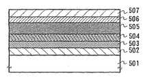
도 3에 도시된 발광 소자는, 캐소드 역할을 하는 제1 전극(502); 높은 전자 수송 특성을 가진 물질에 의해 형성된 제1 층(503); 높은 발광 특성을 가진 물질에 의해 형성된 제2 층(504); 높은 정공 수송 특성을 가진 물질에 의해 형성된 제3 층(505); 산화물 반도체와 금속 산화물로 구성된 그룹으로부터 선택된 화합물, 및 높은 정공 수송 특성을 가진 화합물을 포함하는 제4 층(506); 및, 애노드 역할을 하는 제2 전극(507)을 쌓음으로써 형성된다. 이 외에, 도 3에 도시되어 있는 참조 번호 501은 기판을 나타낸다.The light emitting device shown in FIG. 3 includes a first electrode 502 serving as a cathode; A first layer 503 formed by a material having high electron transport properties; A
상기 실시예에 따르면, 발광 소자는 유리 또는 플라스틱 기판 위에 제조된다. 수동형 발광 장치는 하나의 기판 위에 상기와 같은 복수의 발광 소자를 제조함으로써 제조될 수 있다. 유리 또는 플라스틱 기판 대신, 발광 소자는 박막 트랜지스터(TFT) 어레이 위에 제조될 수 있다. 따라서, TFT에 의해 발광 소자의 구동을 제어하는 능동(또는, 액티브) 매트릭스형 발광 장치가 제조될 수 있다. TFT의 구조는 특별히 제한되지 않는다. TFT는 스태거드형(staggered type) TFT 또는 역 스태거드형(inversely staggered type) TFT 중 어느 하나일 수도 있다. TFT 어레이 기판위에 형성되는 구동 회로는 N-형 TFT 및 P-형 TFT 두 가지 모두에 의해 형성될 수 있다. 선택적으로, 구동 회로는 N-형 TFT 또는 P-형 TFT 중 어느 하나에 의해 형성될 수도 있다.According to this embodiment, the light emitting element is fabricated on a glass or plastic substrate. A passive light emitting device can be manufactured by manufacturing a plurality of light emitting devices as described above on one substrate. Instead of a glass or plastic substrate, a light emitting device can be fabricated on a thin film transistor (TFT) array. Therefore, an active (or active) matrix type light emitting device that controls the driving of the light emitting element by the TFT can be manufactured. The structure of the TFT is not particularly limited. The TFT may be either a staggered type TFT or an inversely staggered type TFT. The driving circuit formed on the TFT array substrate may be formed by both an N-type TFT and a P-type TFT. Alternatively, the driving circuit may be formed by either an N-type TFT or a P-type TFT.
따라서, 층의 결정화는, 산화물 반도체와 금속 산화물로 구성된 그룹에서 선택된 화합물, 및 높은 정공 수송 특성을 가진 물질을 포함하는 층을 포함한 발광 소자에서 억제될 수 있다. 따라서, 층의 결정화로 인한 누설 전류의 발생이 억제될 수 있어, 긴 수명의 발광 소자가 얻어질 수 있다. 산화물 반도체와 금속 산화물로 구성된 그룹으로부터 선택된 화합물, 높은 정공 수송 특성을 가진 물질, 및 높은 입체 장애를 가진 물질을 포함하는 층을 포함한 발광 소자에서는, 층의 결정화가 더욱 억제될 수 있고, 더 긴 수명의 발광 소자가 얻어질 수 있다.
Therefore, the crystallization of the layer can be suppressed in a light emitting device including a compound including a compound selected from the group consisting of an oxide semiconductor and a metal oxide, and a material having a high hole transporting property. Therefore, generation of a leakage current due to crystallization of the layer can be suppressed, and a long-life light emitting element can be obtained. In a light emitting device including a compound selected from the group consisting of an oxide semiconductor and a metal oxide, a material having a high hole transporting property, and a layer including a material having a high steric hindrance, the crystallization of the layer can be further suppressed, Can be obtained.
[예 1][Example 1]
이하, 본 발명에 따른 발광 소자 제조 방법, 및 발광 소자의 특성이 설명된다.Hereinafter, the method of manufacturing the light emitting device and the characteristics of the light emitting device according to the present invention will be described.
제1 전극은 유리 기판 위에 인듐 주석 산화물(ITO)을 증착함으로써 형성되다. 그런 다음, ITO로 증착된 유리 기판이 150℃의 진공에서 30분 동안 처리된다.The first electrode is formed by depositing indium tin oxide (ITO) on a glass substrate. Then, the glass substrate deposited with ITO is processed in a vacuum of 150 DEG C for 30 minutes.
제1 층은 제1 전극 위에 높은 정공 수송 특성을 가진 α-NPD와 몰리브덴 산화물을 공동-증발(또는, '공증착'이라함;co-evaporation)시킴으로써 형성된다. 몰리브덴 산화물과 α-NPD의 무게비는 0.245:1이다. 제1 층은 130nm의 두께를 갖도록 형성된다. 본원에서 사용되는 용어 "공동-증발"은, 하나의 처리실에 제공된 복수의 증발원으로부터 각각의 재료를 증발시키고, 증발된 재료를 기체 상태에서 혼합하여, 혼합된 재료를 대상에 증착하는 방법을 말한다.The first layer is formed by co-evaporating (or 'co-evaporating') α-NPD and molybdenum oxide having high hole transporting properties on the first electrode. The weight ratio of molybdenum oxide to α-NPD is 0.245: 1. The first layer is formed to have a thickness of 130 nm. The term " co-evaporation " as used herein refers to a method of evaporating each material from a plurality of evaporation sources provided in one processing chamber, mixing the vaporized materials in a gaseous state, and depositing the mixed material on the object.
제2 층은 제1 층 위에 α-NPD를 10nm의 두께를 갖도록 기상 증착함으로써 형성된다.The second layer is formed by vapor-depositing? -NPD on the first layer to have a thickness of 10 nm.
제3 층은 제2 층 위에 Alq3와 쿠머린-6을 공동 증발시킴으로써 형성된다. Alq3와 쿠머린-6의 무게비는 1:0.002이다. 제3 층은 37.5nm의 두께를 갖도록 형성된다.The third layer is formed by co-evaporating Alq3 and coumarin-6 on the second layer. The weight ratio of Alq3 to coumarin-6 is 1: 0.002. The third layer is formed to have a thickness of 37.5 nm.
제4 층은 제3 층 위에 37.5nm의 두께를 갖도록 Alq3를 기상 증착함으로써 형성된다.The fourth layer is formed by vapor-depositing Alq3 on the third layer to have a thickness of 37.5 nm.
제5 층은 제4 층 위에 1nm의 두께를 갖도록 플루오르화 칼슘(CaF2)을 기상 증착함으로써 형성된다.The fifth layer is formed by vapor-depositing calcium fluoride (CaF2 ) to have a thickness of 1 nm on the fourth layer.
제2 전극은 제5 층 위에 200nm의 두께를 갖도록 알루미늄을 기상 증착함으로써 형성된다.The second electrode is formed by vapor-depositing aluminum to have a thickness of 200 nm on the fifth layer.
도 1 및 4는 상기와 같이 제조된 발광 소자의 장치 특성을 도시한다.1 and 4 show the device characteristics of the light emitting device manufactured as described above.
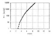
도 4는 예 1에 따라 제조된 발광 소자의 휘도-전압 특성을 도시한다. 도 4에서, 가로축은 인가된 전압(V)을 나타내고, 세로축은 휘도(cd/m2)를 나타낸다. 도 4는, 1cd/m2 이상의 전자발광을 위한 전압인 개시 전압(onset voltage)이 약 2.5V라는 것을 도시한다.4 shows the luminance-voltage characteristics of the light emitting device manufactured according to Example 1. Fig. In Fig. 4, the horizontal axis represents the applied voltage (V), and the vertical axis represents the luminance (cd / m2 ). Fig. 4 shows that the onset voltage, which is the voltage for electroluminescence of1 cd / m2 or more, is about 2.5V.
도 1은 예 1에 따라 제조된 발광 소자의 시간에 따른 휘도 변화의 측정 결과를 도시한다. 도 1에서, 가로축은 시간을 나타내고, 세로축은 휘도를 나타낸다. 휘도는 100의 초기 값을 토대로 초기 값에 대한 그것의 상대적인 값으로 표현된다. 휘도의 변화는 발광 소자에 일정한 양의 전류를 연속적으로 인가함으로써, 즉 발광 소자에 응력을 가함으로써 측정되며, 발광 소자의 휘도는 소정의 시간 간격으로 측정된다. 초기 상태에 1000 cd/m2의 휘도를 가진 전자발광을 얻는데 필요한 전류 밀도를 가진 전류가 인가되며, 상기 인가된 전류에서 얻어진 휘도가 측정된다. 도 1은, 100 시간 후 휘도가 82의 값이 되는데, 즉 휘도가 초기 휘도와 비교하여 18% 감소한다는 것을 나타낸다.
Fig. 1 shows a measurement result of a luminance change with time in a light emitting device manufactured according to Example 1. Fig. In Fig. 1, the horizontal axis represents time and the vertical axis represents luminance. The luminance is expressed as its relative value to the initial value based on the initial value of 100. [ The change in luminance is measured by continuously applying a constant amount of current to the light emitting element, that is, by applying stress to the light emitting element, and the luminance of the light emitting element is measured at predetermined time intervals. In the initial state, a current having a current density necessary for obtaining electroluminescence having a luminance of 1000 cd / m <2 > is applied, and the luminance obtained at the applied current is measured. Figure 1 shows that after 100 hours the luminance is a value of 82, i.e. the luminance is reduced by 18% compared to the initial luminance.
[예 2][Example 2]
본 발명에 따른 발광 소자를 제조하는 방법, 및 발광 소자의 특성이 설명된다.The method of manufacturing the light emitting device according to the present invention, and the characteristics of the light emitting device are described.
제1 전극은 유리 기판 위에 인듐 주석 산화물(ITO)을 증착함으로써 형성된다. ITO로 증착된 유리 기판은 150℃의 진공에서 30분 동안 처리된다.The first electrode is formed by depositing indium tin oxide (ITO) on a glass substrate. The glass substrate deposited with ITO is treated in a vacuum at 150 캜 for 30 minutes.
제1 층은 몰리브덴 산화물, 높은 정공 수송 특성을 가진 α-NPD, 및 높은 입체 장애를 가진 루브린의 공동-증발에 의해 제1 전극 위에 형성된다. 몰리브덴 산화물과 루브린의 무게비는 0.245:0.018이다. 제1 층은 130nm의 두께를 갖도록 형성된다.The first layer is formed on the first electrode by co-evaporation of molybdenum oxide, alpha -NPD with high hole transporting properties, and lubrin with high steric hindrance. The weight ratio of molybdenum oxide to lubrin is 0.245: 0.018. The first layer is formed to have a thickness of 130 nm.
제2 층은 제1 층 위에 10nm의 두께를 갖도록 α-NPD를 기상 증착함으로써 형성된다.The second layer is formed by vapor-depositing? -NPD to have a thickness of 10 nm on the first layer.
제3 층은 제2 층 위에 37.5nm의 두께를 갖도록 Alq3와 쿠머린-6을 공동-증발시킴으로써 형성된다. Alq3와 쿠머린-6의 무게비는 1:0.002이다.The third layer is formed by co-evaporating Alq3 and coumarin-6 to a thickness of 37.5 nm on the second layer. The weight ratio of Alq3 to coumarin-6 is 1: 0.002.
제4 층은 제3 층 위에 37.5nm의 두께를 갖도록 Alq3를 기상 증착함으로써 형성된다.The fourth layer is formed by vapor-depositing Alq3 on the third layer to have a thickness of 37.5 nm.
제5 층은 1nm의 두께를 갖도록 제4 층 위에 플루오르화 칼슘(CaF2)을 기상 증착함으로써 형성된다.The fifth layer is formed by vapor-depositing calcium fluoride (CaF2 ) on the fourth layer to have a thickness of 1 nm.
제2 전극은 200nm의 두께를 갖도록 제5 층 위에 알루미늄을 기상 증착함으로써 형성된다.The second electrode is formed by vapor-depositing aluminum on the fifth layer to have a thickness of 200 nm.
도 1 및 4는 이와 같이 제조된 발광 소자의 장치 특성을 도시한다. 제조 방법 등은 예 1에서 설명된 것과 동일하다.1 and 4 show the device characteristics of the light emitting device thus manufactured. The manufacturing method and the like are the same as those described in Example 1.
도 4는 1cd/m2의 전자발광을 위한 전압인 개시 전압이 약 2.5V라는 것을 나타낸다.4 shows that the starting voltage, which is the voltage for1 cd / m2 of electroluminescence, is about 2.5 V.
도 1은, 100 시간 후 휘도가 92의 값이 된다는 것, 즉 휘도가 초기 휘도와 비교하여 8% 감소된다는 것을 나타낸다.
Figure 1 shows that after 100 hours the luminance becomes a value of 92, i.e. the luminance is reduced by 8% compared to the initial luminance.
[예 3][Example 3]
본 발명에 따른 발광 소자를 제조하는 방법, 및 발광 소자의 특성이 설명된다.The method of manufacturing the light emitting device according to the present invention, and the characteristics of the light emitting device are described.
제1 전극은 유리 기판 위에 인듐 주석 산화물(ITO)을 증착함으로써 형성된다. ITO로 증착된 유리 기판은 150℃의 진공에서 30분 동안 처리된다.The first electrode is formed by depositing indium tin oxide (ITO) on a glass substrate. The glass substrate deposited with ITO is treated in a vacuum at 150 캜 for 30 minutes.
제1 층은 몰리브덴 산화물, 높은 정공 수송 특성을 가진 4,4-비스(N-(4-(N,N-디-엠-트릴아미노)페닐)-N-페닐아미노)바이페닐(4,4-bis(N-(4-(N,N-di-m-trylamino)phenyl)-N-phenylamino)biphenyl)(약어 DNTPD), 및 높은 입체 장애를 가진 루브린의 공동-증발에 의해 제1 전극 위에 형성된다. 물리브덴 산화물, DNTPD, 및 루브린의 무게비는 0.5:1:0.05이다. 제1 층은 120nm의 두께를 갖도록 형성된다.The first layer is made of molybdenum oxide, 4,4-bis (N- (4- (N, N-di-M -tyrylamino) phenyl) -N-phenylamino) biphenyl -bis (co-evaporation of lubrin with high steric hindrance) and the first electrode (e. g., N- (4- (N, N-di-methylamino) phenyl) / RTI > The weight ratio of physical bdden oxide, DNTPD, and lubrin is 0.5: 1: 0.05. The first layer is formed to have a thickness of 120 nm.
제2 층은 제1 층 위에 10nm의 두께를 갖도록 α-NPD를 기상 증착함으로써 형성된다.The second layer is formed by vapor-depositing? -NPD to have a thickness of 10 nm on the first layer.
제3 층은 제2 층 위에 37.5nm의 두께를 갖도록 Alq3 와 쿠머린-6을 공동-증발시킴으로써 형성된다. Alq3 와 쿠머린-6의 무게비는 1:0.003이다.The third layer is formed by co-evaporating Alq3 and coumarin-6 to a thickness of 37.5 nm on the second layer. The weight ratio of Alq3 to coumarin-6 is 1: 0.003.
제4 층은 제3 층 위에 37.5nm의 두께를 갖도록 Alq3를 기상 증착함으로써 형성된다.The fourth layer is formed by vapor-depositing Alq3 on the third layer to have a thickness of 37.5 nm.
제5 층은 제4 층 위에 1nm의 두께를 갖도록 플루오르화 칼슘(CaF2)을 기상 증착함으로써 형성된다.The fifth layer is formed by vapor-depositing calcium fluoride (CaF2 ) to have a thickness of 1 nm on the fourth layer.
제2 전극은 제5 층 위에 200nm의 두께를 갖도록 알루미늄을 기상 증착함으로써 형성된다.The second electrode is formed by vapor-depositing aluminum to have a thickness of 200 nm on the fifth layer.
도 8 및 9는 상기와 같이 제조된 발광 소자의 장치 특성을 도시한다. 측정 방법 등은 예 1에서 설명된 것과 동일하다. 도 8에 있어서, 가로축은 인가된 전압(V)을 나타내고, 세로축은 휘도(cd/m2)를 나타낸다. 도 9에 있어서, 가로축은 시간을 나타내고, 세로축은 휘도(상대적인 값)를 나타낸다.8 and 9 show device characteristics of the light emitting device manufactured as described above. The measurement method and the like are the same as those described in Example 1. 8, the horizontal axis represents the applied voltage (V), and the vertical axis represents the luminance (cd / m2 ). In Fig. 9, the horizontal axis represents time and the vertical axis represents brightness (relative value).
도 8은 1cd/m2 이상의 전자발광을 위한 전압인 개시 전압이 약 2.4V 라는 것을 도시한다.FIG. 8 shows that the starting voltage, which is the voltage for electroluminescence of1 cd / m2 or more, is about 2.4 V.
도 9는 100 시간 후 휘도가 93의 값이 된다는 것, 즉 초기 휘도와 비교해 휘도가 7% 감소된다는 것을 도시한다.
Fig. 9 shows that after 100 hours, the luminance becomes a value of 93, that is, the luminance is reduced by 7% as compared with the initial luminance.
[비교예 1][Comparative Example 1]
비교예로서, 제2 층이 몰리브덴 산화물에 의해서만 형성되는 발광 소자를 제조하는 방법, 및 발광 소자의 장치 특성이 설명된다.As a comparative example, a method of manufacturing a light emitting device in which the second layer is formed only by molybdenum oxide and device characteristics of the light emitting device are described.
인듐 주석 산화물(ITO)이 유리 기판 위에 증착되어 제1 전극을 형성한다. ITO로 증착된 유리 기판은 150℃의 진공에서 30분 동안 처리된다.Indium tin oxide (ITO) is deposited on the glass substrate to form the first electrode. The glass substrate deposited with ITO is treated in a vacuum at 150 캜 for 30 minutes.
제1 층은 제1 전극 위에 100nm의 두께를 갖도록 몰리브덴 산화물을 기상 증착함으로써 형성된다.The first layer is formed by vapor-depositing molybdenum oxide to have a thickness of 100 nm on the first electrode.
제2 층은 제1 층 위에 60nm의 두께를 갖도록 α-NPD를 기상 증착함으로써 형성된다.The second layer is formed by vapor-depositing? -NPD to have a thickness of 60 nm on the first layer.
제3 층은 제2 층 위에 37.5nm의 두께를 갖도록 Alq3 와 쿠머린-6을 공동-증발시킴으로써 형성된다. Alq3 와 쿠머린-6의 무게비는 1:0.002이다.The third layer is formed by co-evaporating Alq3 and coumarin-6 to a thickness of 37.5 nm on the second layer. The weight ratio of Alq3 to coumarin-6 is 1: 0.002.
제4 층은 제3 층 위에 37.5nm의 두께를 갖도록 Alq3를 기상 증착함으로써 형성된다.The fourth layer is formed by vapor-depositing Alq3 on the third layer to have a thickness of 37.5 nm.
제5 층은 제4 층 위에 1nm의 두께를 갖도록 플루오르화 칼슘(CaF2)을 기상 증착함으로써 형성된다.The fifth layer is formed by vapor-depositing calcium fluoride (CaF2 ) to have a thickness of 1 nm on the fourth layer.
제2 전극은 제5 층 위에 200nm의 두께를 갖도록 알루미늄을 기상 증착함으로써 형성된다.The second electrode is formed by vapor-depositing aluminum to have a thickness of 200 nm on the fifth layer.
도 1 및 4는 상기와 같이 제조된 발광 소자의 장치 특성을 도시한다. 측정 방법 등은 예 1에서 설명된 것과 동일하다.1 and 4 show the device characteristics of the light emitting device manufactured as described above. The measurement method and the like are the same as those described in Example 1.
도 4는, 1cd/m2 이상의 전자발광을 위한 전압인 개시 전압이 대략 2.5V임을 도시한다.Fig. 4 shows that the starting voltage, which is the voltage for electron emission of1 cd / m <2 > or more, is approximately 2.5 V.
도 1은, 비교예에 따른 발광 소자의 휘도가 100 시간 후 급격히 감소하여, 발광이 발생될 수 없다는 것을 나타낸다. 이는, 제2 층의 결정화로 인해 누설 전류가 발생된다는 사실 때문이다.Fig. 1 shows that the luminance of the light emitting device according to the comparative example sharply decreases after 100 hours, and luminescence can not be generated. This is due to the fact that a leakage current is generated due to the crystallization of the second layer.
따라서, 예 1 또는 2에서 설명된 발광 소자는 비교예에서 설명된 발광 소자에 대해 동일한 구동 전압에서 빛을 방출한다. 몰리브덴 산화물에 의해서만 형성된 층을 가진 발광 소자와 동일하게, 본 발명에 따른 발광 소자는 낮은 전압에서 동작한다. 예 1 또는 2에서 설명된 발광 소자의 수명은 연장될 수 있다. 이는, 루브린과 같은 높은 입체 장애를 가진 화합물 또는 α-NPD와 같이 높은 수송 특성을 가진 화합물과 혼합됨으로써 P-형 화합물의 결정화가 억제된다는 사실에서 비롯된다.
Therefore, the light-emitting element described in Example 1 or 2 emits light at the same drive voltage for the light-emitting element described in the comparative example. Like the light emitting device having a layer formed only by molybdenum oxide, the light emitting device according to the present invention operates at a low voltage. The lifetime of the light emitting element described in Example 1 or 2 can be extended. This results from the fact that the crystallization of the P-type compound is inhibited by being mixed with a compound having a high steric hindrance such as lubrin or a compound having a high transporting property such as alpha -NPD.
[예 4][Example 4]
본 발명에 따른 발광 소자를 가진 능동 매트릭스형 발광 장치가 예 4에서 설명된다.An active matrix type light emitting device having a light emitting element according to the present invention is described in Example 4. [
도 5를 보면, 본 발명에 따른 발광 소자(92) 및 구동 트랜지스터(91)가 기판(90)에 제공된다. 발광 소자를 구동하기 위한 구동 트랜지스터(91)는 본 발명에 따른 발광 소자(92)에 전기 접속된다. 본원에서 사용되는 용어 "발광 소자"는, 전극(93)과 전극(94) 사이에 발광층을 포함하고, 몰리브덴 산화물, 높은 수송 특성을 가진 물질, 높은 입체 장애를 가진 물질을 포함하는 층을 부분적으로 포함하는 층을 말한다. 발광 소자(92)는 뱅크 층(bank layer)(95)에 의해 분리된다.5, a
본 발명에 따른 발광 소자는, 애노드 역할을 하는 전극이 하위(lower)측(용어 "하위"라 함은 구동 트랜지스터가 발광 소자에 응답하여 제공되는 영역을 말함)에 놓이고, 캐소드 역할을 하는 전극이 상위(upper)측(용어 "상위"라 함은 구동 트랜지스터가 발광 소자에 응답하여 제공되지 않는 영역을 말함)에 놓이는 구조를 가질 수 있다. 선택적으로, 발광 소자는, 캐소드 역할을 하는 전극이 하위측에 놓이고, 애노드 역할을 하는 전극이 상위측에 놓이는 구조를 가질 수도 있다.In the light emitting element according to the present invention, the electrode serving as the anode is placed on the lower side (the term "lower" refers to a region where the driving transistor is provided in response to the light emitting element) And the upper side (the term "upper" refers to an area where the driving transistor is not provided in response to the light emitting element). Alternatively, the light emitting element may have a structure in which an electrode serving as a cathode lies on a lower side and an electrode serving as an anode lies on an upper side.
전자의 경우, 구동 트랜지스터(91)는 p-채널형이고, 후자의 경우, 구동 트랜지스터(91)는 n-채널형이다. 구동 트랜지스터(91)는 스태거드형 또는 역스태거드형 중 어느 한 형태일 수 있다. 구동 트랜지스터(91)의 반도체 층은 결정성 반도체층, 비결정성 반도체층, 또는 세미아모퍼스 반도체층 중 어느 하나일 수 있다.In the former case, the driving
세미아모퍼스 반도체는 비결정성 구조와 결정 구조 사이의 중간 구조를 갖는다(단결정 및 다결정을 포함함). 세미아모퍼스 반도체는 자유 에너지에 대해 안정한 제3 상태를 가지며, 단거리 질서(short-range order)와 격자 왜곡(lattice distortion)을 가진 결정 영역을 갖는다. 반도체의 적어도 일부는 0.5 내지 20nm의 입자 직경을 가진 결정 입자이다. 라만 스펙트럼(raman spectrum)은 520cm-1 보다 낮은 파수로 이동한다. X-선 회절을 이용하여, Si 결정 격자로부터 얻어질 수 있는 회절 피크(111), (220)가 관찰된다. 1 원자% 이상의 수소 또는 할로겐이 미결합 본드(dangling bond)에 대한 중화제로서 반도체에 포함된다. 이러한 반도체를 소위 미결정 반도체라 한다. 규소화합물 기체는 글로우 방전 분해(glow discharge decomposition)(플라즈마 CVD)에 의해 형성된다. 규소화합물 기체로는, SiH4 외에, Si2H6, SiH2Cl2, SiHCl3, SiCl4, SiF4 등이 사용될 수 있다. 규소화합물 기체는 H2, 및 He, Ar, Kr 및 Ne로 구성된 그룹에서 선택된 하나 또는 복수의 희유 기체(rare gas) 원소와 H2에 의해 희석될 수 있다. 희석률은 2 내지 1000배의 범위내에 있다. 인가된 전압은 0.1 내지 133 Pa의 범위내에 있다. 전원 주파수는 1 내지 120 MHz의 범위, 바람직하게는 13 내지 60 MHz의 범위내에 있다. 기판에 대한 가열 온도는 최대 300℃, 바람직하게는 100 내지 250℃ 이다. 반도체막내의 불순물 원소로서, 산소, 질소, 탄소 등의 대기 성분이 최대 1 × 10²⁰/cm3 의 농도를 갖는 것이 바람직하며, 특히 산소 농도는 최대 5 × 10¹⁹/cm3, 바람직하게는 1 ×1019cm3이다. 세미아모퍼스 반도체를 포함하는 TFT(박막 트랜지스터)는 대략 1 내지 10 m2/Vsec의 이동도를 갖는다.Semi-amorphous semiconductors have an intermediate structure between amorphous and crystalline structures (including single crystals and polycrystals). Semi-amorphous semiconductors have a stable third state with respect to free energy and have crystal domains with short-range order and lattice distortion. At least a part of the semiconductor is a crystal grain having a particle diameter of 0.5 to 20 nm. The Raman spectrum travels at a frequency lower than 520 cm <-1 & gt ;. Using X-ray diffraction, diffraction peaks 111 and 220 that can be obtained from the Si crystal lattice are observed. At least 1 atomic percent of hydrogen or halogen is included in the semiconductor as a neutralizing agent for the unbound bond. Such a semiconductor is called a so-called microcrystalline semiconductor. The silicon compound gas is formed by glow discharge decomposition (plasma CVD). As the silicon compound gas, besides SiH4 , Si2 H6 , SiH2 Cl2 , SiHCl3 , SiCl4 , SiF4, and the like can be used. The silicon compound gas may be diluted with H2 and one or more rare gas elements selected from the group consisting of H2 , He, Ar, Kr and Ne. The dilution rate is in the range of 2 to 1000 times. The applied voltage is in the range of 0.1 to 133 Pa. The power supply frequency is in the range of 1 to 120 MHz, preferably in the range of 13 to 60 MHz. The heating temperature for the substrate is at most 300 캜, preferably 100 to 250 캜. As an impurity element in the semiconductor film, oxygen, nitrogen, preferably air components such as carbon having a concentration of up to 1 × 10²⁰ / cm3, and in particular an oxygen content of up to 5 × 10¹⁹ / cm3, preferably from 1 × 1019 cm3 . A TFT (thin film transistor) including a semi-amorphous semiconductor has a mobility of approximately 1 to 10 m2 / Vsec.
애노드 역할을 하는 전극 또는 캐소드 역할을 하는 전극 중 어느 한 전극, 또는 이들 두 전극 모두가 투광성을 갖는 재료로 형성된다.Either one of an electrode serving as an anode or an electrode serving as a cathode, or both of these electrodes are formed of a material having a light transmitting property.
애노드 역할을 하는 전극이 하위측에 놓이고, 애노드 역할을 하는 전극만이 투광성을 가진 물질에 의해 형성되는 경우; 빛은 도 5a에 도시되어 있는 바와 같이 구동 트랜지스터가 제공된 측으로부터 방출된다. 또한, 캐소드 역할을 하는 전극이 하위측에 놓이고, 캐소드 역할을 하는 전극만이 투광성을 가진 재료로 형성되는 경우, 빛은 도 5a에 도시되어 있는 바와 같이 구동 트랜지스터가 제공된 측을 통해 방출된다. 애노드 역할을 하는 전극이 하위측에 놓이고, 캐소드 역할을 하는 전극만이 투광성을 가진 재료로 형성되는 경우, 빛은 도 5b에 도시되어 있는 바와 같이 구동 트랜지스터가 제공된 반대측을 통해 방출된다. 캐소드 역할을 하는 전극이 하위측에 놓이고, 애노드 역할을 하는 전극만이 투광성을 가진 재료로 형성되는 경우, 빛은 도 5b에 도시되어 있는 바와 같이 구동 트랜지스터가 제공된 반대측을 통해 방출된다. 애노드 역할을 하는 전극 및 캐소드 역할을 하는 전극 두 가지 모두가 투광성을 가진 재료로 형성되는 경우, 전극이 하위측에 제공되는지 또는 상위측에 제공되는지에 관계없이, 빛은 도 5c에 도시되어 있는 바와 같이 양측으로부터 방출된다.When the electrode serving as the anode is placed on the lower side and only the electrode serving as the anode is formed by the light-transmitting substance; Light is emitted from the side where the driving transistor is provided as shown in Fig. 5A. Also, in the case where the electrode serving as the cathode lies on the lower side and only the electrode serving as the cathode is formed of a material having translucency, light is emitted through the side provided with the driving transistor as shown in Fig. 5A. If only the electrode serving as the anode is placed on the lower side and only the electrode serving as the cathode is formed of the light-transmitting material, the light is emitted through the opposite side provided with the driving transistor as shown in Fig. 5B. When only the electrode serving as the cathode is placed on the lower side and only the electrode serving as the anode is formed of the light-transmitting material, the light is emitted through the opposite side provided with the driving transistor as shown in Fig. 5B. When both the electrode serving as the anode and the electrode serving as the cathode are formed of a light-transmitting material, regardless of whether the electrode is provided on the lower side or on the upper side, As well as from both sides.
발광 소자는 단색성의 빛, 또는 적색(R), 녹색(G), 청색(B) 등과 같은 완전한 색상의 빛을 방출할 수도 있다. 각 발광 소자는 뱅크 층에 의해 분리되는 것이 바람직하다. 뱅크 층은 무기 물질 또는 유기 물질 중 어느 한 물질을 포함하거나, 무기 물질 및 유기 물질 두 가지 모두를 포함하는 재료에 의해 형성될 수도 있다. 예컨대, 실리콘 산화막이 사용될 수도 있다. 아크릴, 폴리이미드, 및 (실리콘(Si)과 산소(O)의 결합에 의해 골격이 형성되고; 적어도 수소가 치환기로서 포함되거나, 플루오르, 알킬기, 및 방향족 탄화수소로 구성된 그룹에서 선택된 적어도 한 원소가 치환기로서 포함되는 물질) 등에 의해 형성된 골격 구조를 가진 재료가 또한 사용될 수도 있다. 또한, 뱅크 층은 그 곡률 반경이 연속해서 변하는 구부러진 모서리부를 갖도록 형성되는 것이 바람직하다.The light emitting device may emit monochromatic light or full color light such as red (R), green (G), blue (B), and the like. Each light emitting element is preferably separated by a bank layer. The bank layer may include any one of an inorganic material or an organic material, or may be formed of a material including both an inorganic material and an organic material. For example, a silicon oxide film may be used. Wherein at least one element selected from the group consisting of fluorine, alkyl groups, and aromatic hydrocarbons is substituted with a substituent (s) Or the like) may be also used. Further, it is preferable that the bank layer is formed to have a curved corner portion whose radius of curvature changes continuously.
본 발명에 따른 발광 소자는 긴 수명을 갖기 때문에, 본 발명을 수행하여 제조된 발광 장치는 장시간 동안 화상을 표시하고 빛을 방출할 수 있다.
Since the light emitting device according to the present invention has a long lifetime, the light emitting device manufactured by the present invention can display images and emit light for a long time.
[예 5][Example 5]
예 4에 나타나있는 바와 같은 본 발명에 따른 발광 소자를 포함하는 발광 장치는 외부 입력 단자를 부착한 후 다양한 전기 기기에 장착된다.The light emitting device including the light emitting device according to the present invention as shown in Example 4 is mounted on various electric devices after attaching the external input terminal.
본 발명을 수행함으로써 제조된 이러한 전기 기기는 장시간 동안 고품질의 화상을 표시할 수 있다. 이것은 본 발명에 따른 발광 소자가 긴 수명을 갖는다는 사실에서 비롯된다.Such an electric appliance manufactured by carrying out the present invention can display a high-quality image for a long time. This results from the fact that the light emitting device according to the present invention has a long lifetime.
예 5에서는, 도 6 및 7을 참조하여, 발광 소자를 포함하는 발광 장치 및 상기 발광 소자를 장착한 전기 기기가 설명된다.In Example 5, a light-emitting device including a light-emitting element and an electric device equipped with the light-emitting element are described with reference to Figs. 6 and 7. Fig.
도 6은 본 발명에 따른 발광 소자를 포함하는 발광 장치의 상부도이다. 도 7은 오로지 전기 기기의 한 실시예이며, 발광 장치의 구조가 이것으로 제한되지는 않는다.6 is a top view of a light emitting device including a light emitting device according to the present invention. Fig. 7 is only an embodiment of the electric device, and the structure of the light emitting device is not limited thereto.
도 6에서, 점선으로 표시된 참조 번호 401은 구동 회로부(소스측 구동 회로)를 나타내고; 402는 화소부를 나타내며; 403은 구동 회로부(게이트측 구동 회로)를 나타낸다. 참조 번호 404는 실링(sealing) 기판을 나타내고, 405는 실링제(sealing agent)가 부착되는 부분을 나타낸다.In Fig. 6,
신호는, 외부 입력 단자 역할을 하는 FPC(flexible print circuit)(409)로부터 장치 기판(410)에 제공되는 배선을 통해 영상 신호, 클록 신호, 개시 신호, 리셋 신호 등을 수신하면 소스측 구동 회로(401) 및 게이트측 구동 회로(403)로 입력된다. 도 6에는 FPC만 나타나 있지만, FPC는 인쇄 배선 기판(printed wiring board:PWB)을 구비할 수도 있다. 예 5에 따른 발광 장치는 발광 장치의 본체(main body)일뿐 아니라, FPC 또는 PWB를 구비한 본체를 의미한다.Signal receives a video signal, a clock signal, a start signal, a reset signal, and the like through a wiring provided on the
도 7은 도 6에 도시된 발광 장치가 내장된 전기 기기의 일 실시예이다.FIG. 7 is an embodiment of an electric device in which the light emitting device shown in FIG. 6 is incorporated.
도 7은 본체(5501), 하우징(5502), 디스플레이부(5503), 키보드(5504) 등으로 구성된 본 발명을 수행함으로써 제조된 랩탑(laptop) 컴퓨터를 도시한다. 디스플레이 장치는 본 발명에 따른 발광 소자를 포함하는 발광 장치를 랩탑 컴퓨터에 포함시킴으로써 완성될 수 있다.7 shows a laptop computer manufactured by carrying out the present invention composed of a main body 5501, a housing 5502, a display portion 5503, a keyboard 5504 and the like. The display device can be completed by including a light emitting device including the light emitting device according to the present invention in a laptop computer.
예 5에는 랩탑 컴퓨터가 설명되지만, 셀룰러 전화기, TV 수신 장치, 카 네비게이션(car navigation), 조명 시스템 등이 본 발명에 따른 발광 소자를 포함하는 발광 장치를 내장할 수도 있다.
Although a laptop computer is described in Example 5, a cellular phone, a TV receiver, a car navigation system, a lighting system, and the like may also incorporate a light emitting device including the light emitting device according to the present invention.
[예 6][Example 6]
예 6에서는, 본 발명에 따른 발광 소자를 제조하는 방법, 및 발광 소자의 장치 특성이 설명된다. 예 6에서는, 네 개의 발광 소자, 즉 발광 소자(1), 발광 소자(2), 발광 소자(3), 및 발광 소자(4)가 제조되는데, 이들 모두는 서로 다른 두께를 가진 제1 층을 갖는다.In Example 6, a method of manufacturing the light emitting device according to the present invention and device characteristics of the light emitting device are described. In Example 6, four light emitting elements, i.e., a
제1 전극은 유리 기판 위에 실리콘 산화물을 포함하는 인듐 주석 산화물(ITO)에 의해 형성된다. 다음으로, 제1 전극이 제공된 유리 기판은 150℃ 의 진공에서 30분 동안 처리된다.The first electrode is formed on the glass substrate by indium tin oxide (ITO) containing silicon oxide. Next, the glass substrate provided with the first electrode is processed in a vacuum of 150 DEG C for 30 minutes.
제1 층은 몰리브덴 산화물, 루브린, 및 DNTPD을 각각 0.67:1:0.02의 무게비를 갖도록 제1 전극 위에 공동-증발시킴으로써 형성된다. 발광 소자(1)의 제1 층은 40nm의 두께를 갖도록 형성된다. 발광 소자(2)의 제1 층은 80nm의 두께를 갖도록 형성된다. 발광 소자(3)의 제1 층은 120nm의 두께를 갖도록 형성된다. 발광 소자(4)의 제1 층은 160nm의 두께를 갖도록 형성된다.The first layer is formed by co-evaporating molybdenum oxide, lubrin, and DNTPD onto the first electrode to have a weight ratio of 0.67: 1: 0.02, respectively. The first layer of the light-emitting
제2 층은 제1 층 위에 10nm의 두께를 갖도록 α-NPD를 기상 증착함으로써 형성된다.The second layer is formed by vapor-depositing? -NPD to have a thickness of 10 nm on the first layer.
제3 층은 1:0.005의 무게비를 갖도록 제2 층 위에 Alq3 및 쿠머린-6을 공동-증발시킴으로써 형성된다. 상기 제3 층은 37.5nm의 두께를 갖도록 형성된다.The third layer is formed by co-evaporating Alq3 and coumarin-6 on the second layer to have a weight ratio of 1: 0.005. The third layer is formed to have a thickness of 37.5 nm.
제4 층은 제3 층 위에 37.5nm의 두께를 갖도록 Alq3를 기상 증착함으로써 형성된다.The fourth layer is formed by vapor-depositing Alq3 on the third layer to have a thickness of 37.5 nm.
제5 층은 제4 층 위에 1nm의 두께를 갖도록 플루오르화 리튬(LiF)을 기상 증착함으로써 형성된다.The fifth layer is formed by vapor-depositing lithium fluoride (LiF) to have a thickness of 1 nm on the fourth layer.
제2 전극은 제5 층 위에 200nm의 두께를 갖도록 알루미늄을 기상 증착함으로써 형성된다.The second electrode is formed by vapor-depositing aluminum to have a thickness of 200 nm on the fifth layer.
도 10 및 11은 상기와 같이 제조된 발광 소자의 장치 특성을 도시한다.10 and 11 show the device characteristics of the light emitting device manufactured as described above.
도 10은 예 6에 따라 제조된 발광 소자의 휘도-전압 특성을 도시한다. 도 10에 있어서, 가로축은 전압(V)을 나타내고, 세로축은 휘도(cd/m2)를 나타낸다. 이 외에, 닫힌 원(closed circle)은 발광 소자(1)의 특성을 나타내고; 열린 원(open circle)은 발광 소자(2)의 특성을 나타내고; 닫힌 사각형은 발광 소자(3)의 특성을 나타내며; 열린 사각형은 발광 소자(4)의 특성을 나타낸다. 도 10에는, 1cd/m2 이상의 전자발광을 위한 전압인 개시 전압이 각 발광 소자에서 대략 2.5V라는 것이 도시되어 있다. 개시 전압은 각 발광 소자의 제1 층의 두께에도 불구하고 거의 서로 동일하다. 즉, 본 발명에 의해 실행된 발광 소자에 대한 개시 전압은 제1 층의 두께에 영향을 받지 않는다. 따라서, 발광을 반사하는데 전극이 사용되는 발광 소자로부터의 발광에 대한 외부 결합 효율은, 본 발명에 따른 제1 층의 두께를 변화시켜 광 경로 길이를 제어함으로써 쉽게 개선되게 된다.Fig. 10 shows luminance-voltage characteristics of the light emitting device manufactured according to Example 6. Fig. 10, the horizontal axis represents voltage (V) and the vertical axis represents luminance (cd / m2 ). Besides, the closed circle represents the characteristic of the
도 11은 예 6에 따라 제조된 발광 소자의 시간에 따른 휘도 변화의 측정 결과를 도시한다. 도 11에 있어서, 가로축은 시간을 나타내고, 세로축은 휘도를 나타낸다. 휘도는 100의 초기 값을 토대로 한 초기 휘도에 대한 그것의 상대적인 값으로 표현된다. 휘도의 변화는 발광 소자에 일정한 양의 전류를 연속해서 인가함으로써, 즉 발광 소자에 응력을 가함으로써 측정되며; 발광 소자의 휘도는 소정의 시간 간격으로 측정된다. 초기 상태에서 3000cd/m2의 휘도를 가진 전자발광을 얻는데 필요한 전류 밀도를 가진 전류가 인가되며, 상기 인가된 전류에서 얻어지는 휘도가 측정된다. 도 11은, 100 시간 후 각각의 발광 소자(1), (2), (3), 및 (4)에서 휘도가 초기 휘도에 대해 14% 이하로 감소된다는 것을 도시한다. 따라서, 본 발명에 의해 실행된 발광 소자의 휘도는 거의 저하되지 않는다.
11 shows a measurement result of the luminance change over time of the light emitting device manufactured according to Example 6. Fig. In Fig. 11, the horizontal axis represents time and the vertical axis represents luminance. The luminance is expressed as its relative value to the initial luminance based on the initial value of 100. [ The change in luminance is measured by continuously applying a constant amount of current to the light emitting element, that is, by applying stress to the light emitting element; The luminance of the light emitting element is measured at predetermined time intervals. In the initial state, a current having a current density necessary for obtaining electroluminescence having a brightness of 3000 cd / m <2 > is applied, and the brightness obtained from the applied current is measured. Fig. 11 shows that the luminance in each of the
[예 7][Example 7]
본 발명에 따른 발광 소자를 제조하는 방법 및 발광 소자의 장치 특성이 예 7에서 설명된다. 예 7에는, 9개의 발광 소자, 즉 발광 소자(11), 발광 소자(12), 발광 소자(13), 발광 소자(14), 발광 소자(15), 발광 소자(16), 발광 소자(17), 발광 소자(18), 및 발광 소자(19)가 제조되며, 이들 모두는 상이한 재료로 형성된 제1 전극을 갖는다.The method of manufacturing the light emitting device according to the present invention and the device characteristics of the light emitting device are described in Example 7. In Example 7, nine light emitting elements, namely, a
발광 소자(11)에 대한 제1 전극은 유리 기판 위에 몇몇(several) % 실리콘을 포함하는 알루미늄에 의해 형성된다. 발광 소자(12)에 대한 제1 전극은 유리 기판 위에 몇몇 % 티타늄을 포함하는 알루미늄에 의해 형성된다. 발광 소자(13)의 제1 전극은 유리 기판 위의 티타늄에 의해 형성된다. 발광 소자(14)의 제1 전극은 유리 기판 위의 질화 티타늄에 의해 형성된다. 발광 소자(15)의 제1 전극은 유리 기판 위의 탄탈(tantalum)에 의해 형성된다. 발광 소자(16)의 제1 전극은 유리 기판 위의 질화 탄탈에 의해 형성된다. 발광 소자(17)의 제1 전극은 유리 기판 위의 텅스텐에 의해 형성된다. 발광 소자(18)의 제1 전극은 유리 기판 위의 크롬에 의해 형성된다. 발광 소자(19)의 제1 전극은 유리 기판 위의 몰리브덴에 의해 형성된다.The first electrode for the
다음으로, 제1 전극을 구비한 유리 기판이 150℃의 진공에서 30분 동안 처리된다.Next, the glass substrate provided with the first electrode is processed in a vacuum of 150 캜 for 30 minutes.
제1 층은, 각각 0.1:1:0.02의 무게비를 갖도록 몰리브덴 산화물, 루브린, 및α-NPD를 제1 전극 위에 공동-증발시킴으로써 형성된다. 제1 층은 60nm의 두께를 갖도록 형성된다.The first layer is formed by co-evaporating molybdenum oxide, lubrin, and? -NPD on the first electrode to have a weight ratio of 0.1: 1: 0.02, respectively. The first layer is formed to have a thickness of 60 nm.
제2 층은 제1 층 위에 10nm의 두께를 갖도록 α-NPD를 기상 증착함으로써 형성된다.The second layer is formed by vapor-depositing? -NPD to have a thickness of 10 nm on the first layer.
제3 층은 제2 층 위에 Alq3 및 쿠머린-6을 1:0.005의 무게비를 갖도록 공동-증발시킴으로써 형성된다. 상기 제3 층은 40nm의 두께를 갖도록 형성된다.The third layer is formed by co-evaporating Alq3 and coumarin-6 on the second layer to a weight ratio of 1: 0.005. The third layer is formed to have a thickness of 40 nm.
제4 층은 제3 층 위에 20nm의 두께를 갖도록 Alq3를 기상 증착함으로써 형성된다.The fourth layer is formed by vapor-depositing Alq3 on the third layer to have a thickness of 20 nm.
제5 층은 제4 층 위에 리튬(Li)과 4,4'-비스(5-메틸벤즈옥사졸-2-일)스틸벤(4,4'-bis(5-methylbenzoxazole-2-yl)stilbene)(약어 BzOs)을 각각 0.02:1의 무게비를 갖도록 공동-증발시킴으로써 형성된다. 제5 층은 20nm의 두께를 갖도록 형성된다.The fifth layer is formed by depositing lithium (Li) and 4,4'-bis (5-methylbenzoxazole-2-yl) stilbene ) (Abbreviated BzOs) in a weight ratio of 0.02: 1, respectively. The fifth layer is formed to have a thickness of 20 nm.
제2 전극은 110nm의 두께를 갖도록 제5 층 위의 인듐 주석 산화물(ITO)에 의해 형성된다.The second electrode is formed by indium tin oxide (ITO) on the fifth layer to have a thickness of 110 nm.
1cd/m2 이상의 전자발광을 위한 개시 전압을 측정하기 위해, 제1 전극의 전위가 제2 전극의 전위보다 높도록, 상기와 같이 제조된 각각의 발광 소자에 전압이 인가된다. 도 12는 닫힌 사각형으로 표시된 측정 결과를 도시한다. 도 12에 있어서, 가로축은 제조된 발광 소자를 나타내고, 세로축은 전압(V)을 나타낸다.
A voltage is applied to each light emitting device manufactured as described above so that the potential of the first electrode is higher than the potential of the second electrode in order to measure the initiation voltage for electroluminescence of1 cd / m2 or more. Figure 12 shows the measurement result, indicated by a closed square. 12, the horizontal axis represents the manufactured light emitting device, and the vertical axis represents voltage (V).
[비교예 2][Comparative Example 2]
이하, 예 7에서 설명된 발광 소자에 대한 비교예로서, 발광 소자(21), 발광 소자(22), 발광 소자(23), 발광 소자(24), 발광 소자(25), 발광 소자(26), 발광 소자(27), 발광 소자(28), 및 발광 소자(29)가 설명된다.The
발광 소자(21 내지 29)를 구성하는 각 층은, 발광 소자(21 내지 29) 각각의 제1 층이 구리 프탈로시아닌(copper phthalocyanine)에 의해 형성된다는 점을 제외하고, 동일한 재료에 의해 제조되어 발광 소자(11 내지 19)와 동일한 두께를 갖는다. 발광 소자(21)의 제1 전극은 몇몇 % 실리콘을 포함하는 알루미늄에 의해 형성된다. 발광 소자(22)의 제1 전극은 몇몇 % 티타늄을 포함하는 알루미늄에 의해 형성된다. 발광 소자(23)의 제1 전극은 티타늄에 의해 형성된다. 발광 소자(24)의 제1 전극은 질화 티타늄에 의해 형성된다. 발광 소자(25)의 제1 전극은 탄탈에 의해 형성된다. 발광 소자(26)의 제1 전극은 질화 탄탈에 의해 형성된다. 발광 소자(27)의 제1 전극은 텅스텐에 의해 형성된다. 발광 소자(28)의 제1 전극은 크롬에 의해 형성된다. 발광 소자(29)의 제1 전극은 몰리브덴에 의해 형성된다.Each layer constituting the
1cd/m2이상의 전자발광을 위한 개시 전압을 측정하기 위해, 제1 전극의 전위가 제2 전극의 전위보다 높도록 상기와 같이 제조된 발광 소자 각각에 전압이 인가된다. 도 12는 닫힌 삼각형으로 표시된 측정 결과를 도시한다.In order to measure a starting voltage for electroluminescence of1 cd / m2 or more, a voltage is applied to each of the light emitting devices manufactured as described above such that the potential of the first electrode is higher than the potential of the second electrode. Figure 12 shows the measurement result, indicated by a closed triangle.
도 12는 구리 프탈로시아닌에 의해 형성된 제1 층을 가진 발광 소자(21 내지 29)의 개시 전압이 서로 상이하다는 것, 즉 개시 전압은 제1 전극을 형성하는 재료에 의존한다는 것을 도시한다. 반면, 본 발명에 의해 실행된 발광 소자(11 내지 21)의 개시 전압은 제1 전극을 형성하는 재료에도 불구하고 서로 거의 동일하다. 본 발명에 따른 발광 소자는 전극 등을 형성하는 재료의 종류에 덜 영향을 받는다. 따라서, 발광을 반사하는데 전극이 사용되는 발광 소자가 본 발명에 따라 제조되는 경우, 더 우수한 반사율을 가진 재료에 의해 형성된 전극을 선택하는 것이 용이해진다.Fig. 12 shows that the starting voltages of the
[예 8][Example 8]
이하, 본 발명에 따른 발광 소자를 제조하는 방법 및 발광 소자의 특성이 설명된다. 예 8에서는, 모두가 상이한 두께의 제1 층을 갖는 발광 소자가 제조된다. 발광 소자의 구동 전압의 막 두께 의존성이 나타나게 된다.Hereinafter, the method of manufacturing the light emitting device according to the present invention and the characteristics of the light emitting device will be described. In Example 8, a light emitting device is manufactured in which all of the first layers have different thicknesses. The dependency of the driving voltage of the light emitting element on the film thickness appears.
예 6에서 제조된 발광 소자(1 내지 4)가 샘플로 사용된다. 발광 소자(1)의 제1 층은 40nm의 두께를 갖도록 형성된다. 발광 소자(2)의 제1 층은 80nm의 두께를 갖도록 형성된다. 발광 소자(3)의 제1 층은 120nm의 두께를 갖도록 형성된다. 발광 소자(4)의 제1 층은 160nm의 두께를 갖도록 형성된다.The
제1 전극의 전위가 제2 전극의 전위보다 높도록, 각각의 발광 소자에 전압이 인가된다. 도 13은 발광 소자(1 내지 4)의 전류 밀도-전압 특성을 도시한다. 발광 소자(1 내지 4)의 전류 밀도-전압 특성은 제1 층의 두께에 있어서의 차이에도 불구하고 서로 거의 다르지 않다. 따라서, 몰리브덴 산화물, 루브린, 및 DNTPD에 의해 형성되는 제1 층의 두께 증가가 구동 전압을 증가시키는 결과를 가져오지 않는다.
A voltage is applied to each light emitting element so that the potential of the first electrode is higher than the potential of the second electrode. 13 shows the current density-voltage characteristics of the light-emitting
[비교예 3][Comparative Example 3]
이하, 예 8에서 설명된 발광 소자에 대한 비교예로서, 발광 소자(30), 발광 소자(31), 발광 소자(32), 발광 소자(33), 발광 소자(34), 및 발광 소자(35)가 설명된다.The
발광 소자(30 내지 35)가 제조되는데, 이들 소자 모두는 상이한 두께의 제2 층을 갖는다. 제1 층은 20nm의 두께를 갖도록 구리 프탈로시아닌에 의해 형성된다. 제2 층은 기상 증착을 이용하여 α-NPD에 의해 형성된다. 발광 소자(30)의 제2 층은 60nm의 두께를 갖도록 형성된다. 발광 소자(31)의 제2 층은 80nm의 두께를 갖도록 형성된다. 발광 소자(32)의 제2 층은 100nm의 두께를 갖도록 형성된다. 발광 소자(33)의 제2 층은 120nm의 두께를 갖도록 형성된다. 발광 소자(34)의 제2 층은 140nm의 두께를 갖도록 형성된다. 발광 소자(35)의 제2 층은 160nm의 두께를 갖도록 형성된다.
다음으로, 제3 층은 1:0.005의 무게비를 갖도록 제2 층 위에 Alq3와 쿠머린-6을 공동-증발시킴으로써 형성된다. 제3 층은 37.5nm의 두께를 갖도록 형성된다. 제4 층은 제3 층 위에 37.5nm의 두께를 갖도록 Alq3를 기상 증착함으로써 형성된다. 제5 층은 제4 층 위에 1nm의 두께를 갖도록 플루오르화 칼슘(CaF2)을 기상 증착함으로써 형성된다. 제2 전극은 제5 층 위에 200nm의 두께를 갖도록 알루미늄을 기상 증착함으로써 형성된다.Next, the third layer is formed by co-evaporating Alq3 and coumarin-6 on the second layer to have a weight ratio of 1: 0.005. The third layer is formed to have a thickness of 37.5 nm. The fourth layer is formed by vapor-depositing Alq3 on the third layer to have a thickness of 37.5 nm. The fifth layer is formed by vapor-depositing calcium fluoride (CaF2 ) to have a thickness of 1 nm on the fourth layer. The second electrode is formed by vapor-depositing aluminum to have a thickness of 200 nm on the fifth layer.
각 발광 소자를 작동시키기 위해, 제1 전극의 전위가 제2 전극의 전위보다 높도록 전압이 인가된다. 도 14는 발광 소자(30 내지 35)의 전류 밀도-전압 특성을 도시한다. 발광 소자의 구동 전압은 제2 층의 두께를 증가시키면 증가한다. 따라서, α-NPD에 의해 형성된 제2 층의 두께 증가가 결과적으로 구동 전압의 증가를 가져온다.
In order to operate each light emitting element, a voltage is applied so that the potential of the first electrode is higher than the potential of the second electrode. 14 shows the current density-voltage characteristics of the light-emitting
[비교예 4][Comparative Example 4]
이하, 예 8에서 설명된 발광 소자에 대한 비교예로서, 발광 소자(36), 발광 소자(37), 및 발광 소자(38)가 설명된다. 각 제1 층은 서로 상이한 두께를 갖도록 몰리브덴 산화물에 의해 형성된다. 제2 층은 20nm의 두께를 갖도록 구리 프탈로시아닌에 의해 형성된다. 제3 층은 40nm의 두께를 갖도록 α-NPD를 기상 증착함으로써 형성된다.Hereinafter, the
다음으로, 제4 층은 37.5nm의 두께를 갖도록 제3 층 위에 Alq3와 쿠머린-6을 공동-증발시킴으로써 형성된다. 제5 층은 37.5nm의 두께를 갖도록 제4 층 위에 Alq3를 기상 증착함으로써 형성된다. 제6 층은 1nm의 두께를 갖도록 제5 층 위에 CaF2를 기상 증착함으로써 형성된다. 제7 층은 200nm의 두께를 갖도록 제6 층 위에 알루미늄을 기상 증착함으로써 형성된다.Next, the fourth layer is formed by co-evaporating Alq3 and coumarin-6 on the third layer to have a thickness of 37.5 nm. The fifth layer is formed by vapor-depositing Alq3 on the fourth layer to have a thickness of 37.5 nm. The sixth layer is formed by vapor-depositing CaF2 on the fifth layer to have a thickness of 1 nm. The seventh layer is formed by vapor-depositing aluminum on the sixth layer to have a thickness of 200 nm.
각 발광 소자를 작동시키기 위해, 제1 전극의 전위가 제2 전극의 전위보다 높도록 상기 발광 소자에 전압이 인가된다. 도 15는 발광 소자(36 내지 38)의 전류 밀도-전압 특성을 도시한다. 발광 소자의 구동 전압은 몰리브덴 산화물에 의해 형성된 제1 층의 두께를 증가시킴에 따라 증가한다.In order to operate each light emitting element, a voltage is applied to the light emitting element such that the potential of the first electrode is higher than the potential of the second electrode. Fig. 15 shows current density-voltage characteristics of the
표 1은 예 8, 비교예 3, 및 비교예 4에 의해 제공된 구동 전압의 막 두께 의존성의 결과를 도시한다. 표 1은 발광 소자에 100 mA/cm2의 전류를 인가하는데 필요한 구동 전압의 데이터를 도시한다.Table 1 shows the results of the film thickness dependence of the driving voltage provided by Example 8, Comparative Example 3, and Comparative Example 4. Table 1 shows data of driving voltage required for applying a current of 100 mA / cm <2 > to the light emitting element.
[nm]thickness
[nm]
예 8에서는, 발광 소자(1 내지 4)에 100mA/cm2의 전류를 가하는데 6.1 내지 6.3V의 구동 전압이 필요하다. 반면, 비교예 3에서는, 발광 소자(30 내지 35)에 100mA/cm2의 전류를 가하는데 12.5 내지 19.9V의 구동 전압이 필요하다. 비교예 4에서는, 발광 소자(36 내지 38)에 100mA/cm2의 전류를 가하는데 11.7 내지 12.7V의 구동 전압이 필요하다.In Example 8, a drive voltage of 6.1 to 6.3 V is required to apply a current of 100 mA / cm2 to the light-emitting
표 1에 설명된 결과는, 유기 화합물과 무기물의 혼합물에 의해 형성된 층이 제공된 발광 소자의 구동 전압이 무기 화합물인 몰리브덴 산화물 또는 α-NPD에 의해 형성된 층이 제공된 발광 소자의 구동 전압보다 더 낮을 수 있다는 것을 나타낸다. 더욱이, 상기 결과는 또한, 층의 두께가 증가하는 경우라 하더라도 구동 전압의 증가가 방지될 수 있다는 것을 나타낸다.The results described in Table 1 indicate that the driving voltage of the light emitting element provided with the layer formed by the mixture of the organic compound and the inorganic material may be lower than the driving voltage of the light emitting element provided with the layer formed by molybdenum oxide or? -NPD, which is an inorganic compound Lt; / RTI > Moreover, the above results also indicate that an increase in the driving voltage can be prevented even when the thickness of the layer is increased.
따라서, 구동 전압은 본 발명에 따른 발광 소자를 사용함으로써 감소될 수 있으므로, 발광 소자의 전력 소비가 감소될 수 있다. 또한, 발광 소자의 두께가 증가할 수 있어, 한 쌍의 전극 사이의 단락 회로 저하를 줄일 수 있게 된다.
Therefore, the driving voltage can be reduced by using the light emitting element according to the present invention, so that the power consumption of the light emitting element can be reduced. Further, the thickness of the light emitting element can be increased, and the short circuit deterioration between the pair of electrodes can be reduced.
[예 9][Example 9]
2.4 인치의 화면 크기를 가진 QVGA 능동 매트릭스형 발광 장치의 특성이 예 9에서 설명된다. 능동 매트릭스형 발광 장치는 예 4의 경우에서와 같은 트랜지스터를 이용하여 발광 소자를 구동한다. 발광 장치는 이하에 설명되는 구성을 갖는다.The characteristics of a QVGA active matrix light emitting device having a screen size of 2.4 inches are described in Example 9. [ The active matrix type light emitting device uses the same transistor as in the case of Example 4 to drive the light emitting element. The light emitting device has the configuration described below.
제1 전극은 실리콘 산화물을 포함하는 인듐 주석 산화물에 의해 형성된다. 제1 층은 높은 정공 수송 특성을 가진 α-NPD 또는 몰리브덴 산화물을 제1 전극 위에 공동-증발시킴으로써 형성된다.The first electrode is formed by indium tin oxide containing silicon oxide. The first layer is formed by co-evaporating [alpha] -NPD or molybdenum oxide with high hole transport properties on the first electrode.
제1 층이 120nm의 두께를 갖도록 몰리브덴 산화물과 α-NPD의 혼합물에 의해 형성되는 발광 장치를 발광 장치(1)라 한다. 이와 유사하게, 제1 층이 240nm의 두께를 갖도록 형성되는 발광 장치를 발광 장치(2)라 한다.A light emitting device formed by a mixture of molybdenum oxide and? -NPD so that the first layer has a thickness of 120 nm is referred to as a light emitting device (1). Similarly, a light emitting device formed so that the first layer has a thickness of 240 nm is referred to as a
제2 층은 제1 층 위에 10nm의 두께를 갖도록 α-NPD를 기상 증착함으로써 형성된다. 제3 층은 제2 층 위에 40nm의 두께를 갖도록 Alq3 및 쿠머린-6을 공동-증발시킴으로써 형성된다.The second layer is formed by vapor-depositing? -NPD to have a thickness of 10 nm on the first layer. The third layer is formed by co-evaporating Alq3 and coumarin-6 to have a thickness of 40 nm on the second layer.
제4 층은 제3 층 위에 30nm의 두께를 갖도록 Alq3를 기상 증착함으로써 형성된다. 제5 층은 제4 층 위에 1nm의 두께를 갖도록 플루오르화 칼슘(CaF2)을 기상 증착함으로써 형성된다. 제2 전극은 제5 층 위에 200nm의 두께를 갖도록 알루미늄을 기상 증착함으로써 형성된다.The fourth layer is formed by vapor-depositing Alq3 on the third layer to have a thickness of 30 nm. The fifth layer is formed by vapor-depositing calcium fluoride (CaF2 ) to have a thickness of 1 nm on the fourth layer. The second electrode is formed by vapor-depositing aluminum to have a thickness of 200 nm on the fifth layer.
발광 장치(1 및 2)에서 암점(dark spot)(발광하지 않는 화소)의 수는 전기 전도 시작시, 및 60 시간 동안의 온도 주기 테스트(+85℃ (4시간) 에서 -40℃ (4시간)) 후에 검사된다.The number of dark spots (non-emitting pixels) in the
발광 장치(1)는 전기 전도 시작시에 평균 0.7의 암점 수를 가지며, 온도 주기 테스트 후에는 2.3을 갖는다. 발광 장치(2)는 전기 전도 시작시에 평균 0.5의 암점 수를 가지며, 온도 주기 테스트 이후에 0.5를 갖는다. 본원에서 사용되는 용어 "평균 암점의 수(average of the number of dark spots)"는 발광 장치의 시험된 닫힌 삼각형 수의 평균값을 나타낸다.
The
[비교예 5][Comparative Example 5]
예 9에 대한 비교예로서, 발광 소자가 상이한 구성을 갖는 능동 매트릭스형 발광 장치(3)가 제조된다.As a comparative example to Example 9, the active matrix type
발광 소자는 이하의 방식으로 형성된다. 제1 층은 20nm의 두께를 갖도록 구리 프탈로시아닌에 의해 형성된다. 제2 층은 40nm의 두께를 갖도록 α-NPD에 의해 형성된다. 제3 층은 제2 층 위에 40nm의 두께를 갖도록 Alq3와 쿠머린-6을 공동-증발시킴으로써 형성된다. 제4 층은 제3 층 위에 40nm의 두께를 갖도록 Alq3를 기상 증착함으로써 형성된다. 제5 층은 제4 층 위에 1nm의 두께를 갖도록 플루오르화 칼슘(CaF2)을 기상 증착함으로써 형성된다. 제2 전극은 제5 층 위에 200nm의 두께를 갖도록 알루미늄을 기상 증착함으로써 형성된다.The light emitting element is formed in the following manner. The first layer is formed by copper phthalocyanine to have a thickness of 20 nm. The second layer is formed by? -NPD to have a thickness of 40 nm. The third layer is formed by co-evaporating Alq3 and coumarin-6 to a thickness of 40 nm on the second layer. The fourth layer is formed by vapor-depositing Alq3 on the third layer to have a thickness of 40 nm. The fifth layer is formed by vapor-depositing calcium fluoride (CaF2 ) to have a thickness of 1 nm on the fourth layer. The second electrode is formed by vapor-depositing aluminum to have a thickness of 200 nm on the fifth layer.
발광 장치(3)의 암점의 수는 전기 전도 시작시, 및 60 시간 동안의 온도 주기 테스트(+85℃ (4시간) 에서 -40℃ (4시간)) 이후 검사된다.The number of dark spots in the
발광 장치(3)는 전기 전도 시작시에 평균 18개의 암점 개수를 가지며, 온도 주기 테스트 이후에는 444개를 갖는다. 온도 주기 테스트 이후의 평균 암점의 수는 전기 전도 시작시의 암점의 수에 25배 증가한다.The
표 2는 예 9 및 비교예 5에서 60 시간 동안의 온도 주기 테스트(+85℃ (4시간) 에서 -40℃ (4시간)) 이후의 암점의 수에 대한 결과를 나타낸다.Table 2 shows the results for the number of dark points after the temperature cycle test (+ 85 ° C (4 hours) -40 ° C (4 hours)) for 60 hours in Example 9 and Comparative Example 5.
암점은 전기 전도 시작시에 예 9에 따른 발광 장치(1 및 2)에서는 거의 관찰되지 않으며, 온도 주기 테스트 이후에 증가하지 않는다. 반면, 전기 전도 시작시에 비교예 5에 따른 발광 장치(3)에서는 많은 수의 암점이 관찰되며, 온도 주기 테스트 이후에 전기 전도 시작시의 암점에 25배 증가한다. 상기 결과에 있어서의 차이는, 몰리브덴 산화물과 α-NPD의 혼합물에 의해 형성된 제1 층의 두께가 증가한다는 사실로부터 비롯될 수 있다.The dark spot is hardly observed in the
예 9로부터의 결과는, 암화소(dark pixel) 결함의 수가 발광 소자의 두께를 증가시킴으로써 급격히 감소될 수 있다는 것을 보여준다. 예 8로부터의 결과에 따르면, 구동 전압이 발광 소자의 두께를 증가시킴에 따라 증가하지 않는다는 것이 자명하다. 따라서, 낮은 구동 전압 및 급격히 억제된 암화소 결함을 가진 발광 장치가 본 발명에 따라 제공될 수 있다.
The results from Example 9 show that the number of dark pixel defects can be drastically reduced by increasing the thickness of the light emitting element. According to the results from Example 8, it is apparent that the driving voltage does not increase as the thickness of the light emitting element increases. Therefore, a light emitting device having a low driving voltage and a rapidly suppressed dark pixel defect can be provided according to the present invention.
[예 10][Example 10]
금속 산화물인 몰리브덴 산화물에 의해 형성된 막의 특성, 높은 정공 수송 특성을 가진 유기 화합물인 α-NPD에 의해 형성된 막, 및 몰리브덴 산화물과 α-NPD의 혼합물에 의해 형성된 막이 검사된다. 이들 막은 기상 증착에 의해 형성된다.The film formed by the molybdenum oxide which is the metal oxide, the film formed by the organic compound having the high hole transporting property, alpha -NPD, and the film formed by the mixture of the molybdenum oxide and the alpha -NPD are examined. These films are formed by vapor deposition.
표 3에 나타나있는 바와 같이, 몰리브덴 산화물과 α-NPD의 혼합물에 의해 형성된 막의 이온화 전위는 몰리브덴 산화물에 의해 형성된 막 및 α-NPD에 의해 형성된 막의 이온화 전위보다 약 0.1 내지 0.2 eV 더 낮다. 그 결과, 몰리브덴 산화물과 α-NPD의 혼합물에 의해 형성된 막의 주입 특성이 향상된다.As shown in Table 3, the ionization potential of the film formed by the mixture of molybdenum oxide and? -NPD is about 0.1-0.2 eV lower than the ionization potential of the film formed by molybdenum oxide and the film formed by? -NPD. As a result, the injection property of the film formed by the mixture of molybdenum oxide and? -NPD is improved.
a: mol/mola: mol / mol
b: 이온화 전위(AC-2에 의해 조사된 값)
b: ionization potential (value irradiated by AC-2)
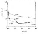
도 16은 상기 막의 흡광도 스펙트럼을 도시한다. 흡광도 스펙트럼에서, 몰리브덴 산화물의 막 및 α-NPD의 막에 대한 스펙트럼은 가시 광선 영역에서 특징적인 피크를 가지지 않는다. 반면, 몰리브덴 산화물과 α-NPD의 혼합물에 의해 형성된 막의 흡광도(OMOx)는 몰리브덴 산화물에 의해 형성된 막의 흡광도보다 낮다. 따라서, 빛의 흡수 손실은 몰리브덴 산화물에 의해 형성된 층을 사용하기보다는 몰리브덴 산화물과 α-NPD의 혼합물에 의해 형성된 층을 사용함으로써 감소될 수 있다.16 shows the absorbance spectrum of the film. In the absorbance spectrum, the spectrum of the film of molybdenum oxide and the film of alpha -NPD does not have a characteristic peak in the visible light region. On the other hand, the absorbance (OMOx) of the film formed by the mixture of molybdenum oxide and alpha -NPD is lower than that of the film formed by molybdenum oxide. Thus, the absorption loss of light can be reduced by using a layer formed by a mixture of molybdenum oxide and alpha -NPD rather than using a layer formed by molybdenum oxide.
도 16에 있어서, 몰리브덴 산화물과 α-NPD의 혼합물에 의해 형성된 막의 스펙트럼은 대략 500nm에서 새롭게 흡수 피크를 갖는다. 흡수 피크는 막에서 α-NPD와 몰리브덴 산화물 사이의 전하-이동 착물(또는, 전하-이동 착체)의 형성으로부터 비롯될 수 있다. 몰리브덴 산화물이 억셉터(acceptor)인 반면, α-NPD는 도너(donor)이다. 또한, α-NPD뿐 아니라, DATPD와 같은 아민계 화합물도 도너 역할을 한다는 것이 확인되었다.In Fig. 16, the spectrum of the film formed by the mixture of molybdenum oxide and? -NPD has a new absorption peak at about 500 nm. The absorption peak may result from the formation of a charge-transfer complex (or charge-transfer complex) between the alpha-NPD and the molybdenum oxide in the film. While molybdenum oxide is an acceptor, a-NPD is a donor. It has also been confirmed that not only α-NPD but also amine-based compounds such as DATPD also act as donors.
예 1 또는 2에서 설명된 바와 같이, 층의 결정화가 억제될 수 있기 때문에, 금속 산화물 그룹에서 선택된 화합물 및 높은 정공 수송 특성을 가진 화합물을 포함한 층을 포함하는 발광 소자에 대해 수명이 연장될 수 있다. 상기 언급된 바와 같이, 유기 재료와 무기 재료의 혼합은 이들 재료를 따로따로 사용함으로써 얻을 수 없는 상승 효과를 발생시킬 수 있다.As described in Example 1 or 2, since the crystallization of the layer can be suppressed, the lifetime can be prolonged for a light-emitting device including a layer containing a compound selected from a metal oxide group and a compound having a high hole transporting property . As mentioned above, the mixing of the organic material and the inorganic material can cause a synergistic effect that can not be obtained by using these materials separately.
첨부 도면을 참조로 예를 통해 본 발명이 충분히 설명되었지만, 당업자들이라면 다양한 변경 및 변형이 가능하다는 것을 알 수 있다. 따라서, 이러한 변경 및 변형이 이하에 설명된 본 발명의 범위에서 벗어나지 않는다면, 이들 모두가 포함되는 것으로 해석된다.Although the present invention has been fully described by way of example and with reference to the accompanying drawings, it will be apparent to those skilled in the art that various modifications and variations are possible. Accordingly, it is intended that all such modifications and variations be included within the scope of the present invention as set forth below.
201: 기판 202: 제 1 전극
203: 제 1 층 204: 제 2 층
205 : 제 3 층 206: 제 4 층
207: 제 2 전극201: substrate 202: first electrode
203: first layer 204: second layer
205: third layer 206: fourth layer
207: second electrode
Claims (35)
Translated fromKorean상기 제 1 전극 위에 형성되며, 방향족 아민 화합물과 몰리브덴 산화물을 포함하는 혼합층;
상기 혼합층 위의 발광층; 및
상기 발광층 위의 제 2 전극을 포함하는 발광장치.
A first electrode;
A mixed layer formed on the first electrode, the mixed layer including an aromatic amine compound and molybdenum oxide;
A light emitting layer on the mixed layer; And
And a second electrode on the light emitting layer.
상기 몰리브덴 산화물은 몰리브덴 3산화물인 것을 특징으로 하는 발광장치.
10. The method of claim 9,
Wherein the molybdenum oxide is molybdenum trioxide.
상기 혼합층은 상기 방향족 아민 화합물과 상기 몰리브덴 산화물의 공증착에 의해 형성되는 것을 특징으로 하는 발광장치.
10. The method of claim 9,
Wherein the mixed layer is formed by co-deposition of the aromatic amine compound and the molybdenum oxide.
상기 방향족 아민 화합물과 상기 몰리브덴 산화물은 상기 혼합층 내에 혼합되어 있는 것을 특징으로 하는 발광장치.10. The method of claim 9,
Wherein the aromatic amine compound and the molybdenum oxide are mixed in the mixed layer.
상기 방향족 아민 화합물과 상기 몰리브덴 산화물의 전하 이동 착체는 상기 혼합층 내에 형성되어 있는 것을 특징으로 하는 발광장치.
10. The method of claim 9,
Wherein the aromatic amine compound and the charge transfer complex of the molybdenum oxide are formed in the mixed layer.
상기 방향족 아민 화합물은,
4,4'-비스[N-(1-나프틸)-N-페닐-아미노]-바이페닐(4,4'-bis[N-(1-naphtyl)-N-phenyl-amino]-biphenyl),
4,4'-비스[N-(3-메틸페닐)-N-페닐-아미노]-바이페닐(4,4'-bis[N-(3-methylphenyl)-N-phenyl-amino]-biphenyl),
4,4',4"-트리스(N,N-디페닐-아미노)-트리페닐아민(4,4',4"-tris(N,N-diphenyl-amino)-triphenylamine),
4,4',4"-트리스[N-(3-메틸페닐)-N-페닐-아미노]-트리페닐아민(4,4',4"-tris[N-(3-methylphenyl)-N-phenyl-amino]-triphenylamine)으로부터 선택되는 것을 특징으로 하는 발광장치.
10. The method of claim 9,
The aromatic amine compound may be,
Bis [N- (1-naphthyl) -N-phenyl-amino] -biphenyl) -4,4'-bis [N- (1-naphthyl) ,
Bis [N- (3-methylphenyl) -N-phenyl-amino] -biphenyl,
4,4 ', 4 "-tris (N, N-diphenyl-amino) -triphenylamine,
4,4 ', 4 "-tris [N - (3-methylphenyl) -N-phenyl -amino] -triphenylamine). < / RTI >
상기 혼합층의 두께는 40nm이상인 발광장치.
10. The method of claim 9,
Wherein the mixed layer has a thickness of 40 nm or more.
상기 제 1 전극과 상기 제 2 전극 중 적어도 하나는 투광성을 갖는 것을 특징으로 하는 발광장치.
10. The method of claim 9,
Wherein at least one of the first electrode and the second electrode has a light-transmitting property.
상기 방향족 아민 화합물은 10-6cm2/Vs 이상의 정공 이동도를 갖는 것을 특징으로 하는 발광장치.
10. The method of claim 9,
The aromatic amine compound is 10-6 cm2 / Vs. ≪ / RTI >
An active matrix type light emitting device comprising the light emitting device according to any one of claims 9 to 20.
A lighting device comprising the light emitting device according to any one of claims 9 to 12.
상기 제 1 전극 위에 방향족 아민 화합물과 몰리브덴 산화물을 포함하는 혼합층을 형성하는 단계;
상기 혼합층 위에 발광층을 형성하는 단계; 및
상기 발광층 위에 제 2 전극을 형성하는 단계를 포함하는 발광소자의 제조방법.
Forming a first electrode;
Forming a mixed layer including an aromatic amine compound and molybdenum oxide on the first electrode;
Forming a light emitting layer on the mixed layer; And
And forming a second electrode on the light emitting layer.
방향족 아민 화합물과 몰리브덴 산화물을 공증착하여, 상기 제 1 전극 위에 상기 방향족 아민 화합물과 상기 몰리브덴 산화물을 포함하는 혼합층을 형성하는 단계;
상기 혼합층 위에 발광층을 형성하는 단계; 및
상기 발광층 위에 제 2 전극을 형성하는 단계를 포함하는 발광소자의 제조방법.
Forming a first electrode;
Depositing an aromatic amine compound and an oxide of molybdenum on the first electrode to form a mixed layer comprising the aromatic amine compound and the molybdenum oxide on the first electrode;
Forming a light emitting layer on the mixed layer; And
And forming a second electrode on the light emitting layer.
상기 몰리브덴 산화물은 몰리브덴 3산화물인 것을 특징으로 하는 발광소자의 제조방법.
30. The method of claim 28 or 29,
Wherein the molybdenum oxide is molybdenum trioxide.
상기 방향족 아민 화합물은,
4,4'-비스[N-(1-나프틸)-N-페닐-아미노]-바이페닐(4,4'-bis[N-(1-naphtyl)-N-phenyl-amino]-biphenyl),
4,4'-비스[N-(3-메틸페닐)-N-페닐-아미노]-바이페닐(4,4'-bis[N-(3-methylphenyl)-N-phenyl-amino]-biphenyl),
4,4',4"-트리스(N,N-디페닐-아미노)-트리페닐아민(4,4',4"-tris(N,N-diphenyl-amino)-triphenylamine),
4,4',4"-트리스[N-(3-메틸페닐)-N-페닐-아미노]-트리페닐아민(4,4',4"-tris[N-(3-methylphenyl)-N-phenyl-amino]-triphenylamine)으로부터 선택되는 것을 특징으로 하는 발광소자의 제조방법.
30. The method of claim 28 or 29,
The aromatic amine compound may be,
Bis [N- (1-naphthyl) -N-phenyl-amino] -biphenyl) -4,4'-bis [N- (1-naphthyl) ,
Bis [N- (3-methylphenyl) -N-phenyl-amino] -biphenyl,
4,4 ', 4 "-tris (N, N-diphenyl-amino) -triphenylamine,
4,4 ', 4 "-tris [N - (3-methylphenyl) -N-phenyl -amino] -triphenylamine). < / RTI >
상기 방향족 아민 화합물은 10-6cm2/Vs 이상의 정공 이동도를 갖는 것을 특징으로 하는 발광소자의 제조방법.
30. The method of claim 28 or 29,
The aromatic amine compound is 10-6 cm2 / Vs. ≪ / RTI >
상기 제 1 전극과 상기 제 2 전극 중 적어도 하나는 투광성을 갖는 것을 특징으로 하는 발광소자의 제조방법.
30. The method of claim 28 or 29,
Wherein at least one of the first electrode and the second electrode has a light-transmitting property.
Applications Claiming Priority (3)
| Application Number | Priority Date | Filing Date | Title |
|---|---|---|---|
| JP2003336295 | 2003-09-26 | ||
| JPJP-P-2003-336295 | 2003-09-26 | ||
| PCT/JP2004/014412WO2005031798A2 (en) | 2003-09-26 | 2004-09-24 | Light-emitting device and method for manufacturing the same |
Related Parent Applications (1)
| Application Number | Title | Priority Date | Filing Date |
|---|---|---|---|
| KR1020067005626ADivisionKR101286221B1 (en) | 2003-09-26 | 2004-09-24 | Light-emitting device |
Related Child Applications (1)
| Application Number | Title | Priority Date | Filing Date |
|---|---|---|---|
| KR1020127010680ADivisionKR20120062911A (en) | 2003-09-26 | 2004-09-24 | Composite material and method for manufacturing composite material |
Publications (2)
| Publication Number | Publication Date |
|---|---|
| KR20120014044A KR20120014044A (en) | 2012-02-15 |
| KR101590148B1true KR101590148B1 (en) | 2016-01-29 |
Family
ID=34386090
Family Applications (7)
| Application Number | Title | Priority Date | Filing Date |
|---|---|---|---|
| KR1020117030615AExpired - Fee RelatedKR101590148B1 (en) | 2003-09-26 | 2004-09-24 | Light emitting device and method for manufacturing light emitting element |
| KR1020147023148ACeasedKR20140107696A (en) | 2003-09-26 | 2004-09-24 | Light emitting device |
| KR1020127010680ACeasedKR20120062911A (en) | 2003-09-26 | 2004-09-24 | Composite material and method for manufacturing composite material |
| KR1020137011242ACeasedKR20130062367A (en) | 2003-09-26 | 2004-09-24 | Light emitting device |
| KR1020067005626AExpired - Fee RelatedKR101286221B1 (en) | 2003-09-26 | 2004-09-24 | Light-emitting device |
| KR1020097018993AExpired - Fee RelatedKR101286219B1 (en) | 2003-09-26 | 2004-09-24 | A method for manufacturing a light-emitting element |
| KR1020097018994ACeasedKR20090111869A (en) | 2003-09-26 | 2004-09-24 | Lighting system |
Family Applications After (6)
| Application Number | Title | Priority Date | Filing Date |
|---|---|---|---|
| KR1020147023148ACeasedKR20140107696A (en) | 2003-09-26 | 2004-09-24 | Light emitting device |
| KR1020127010680ACeasedKR20120062911A (en) | 2003-09-26 | 2004-09-24 | Composite material and method for manufacturing composite material |
| KR1020137011242ACeasedKR20130062367A (en) | 2003-09-26 | 2004-09-24 | Light emitting device |
| KR1020067005626AExpired - Fee RelatedKR101286221B1 (en) | 2003-09-26 | 2004-09-24 | Light-emitting device |
| KR1020097018993AExpired - Fee RelatedKR101286219B1 (en) | 2003-09-26 | 2004-09-24 | A method for manufacturing a light-emitting element |
| KR1020097018994ACeasedKR20090111869A (en) | 2003-09-26 | 2004-09-24 | Lighting system |
Country Status (6)
| Country | Link |
|---|---|
| US (4) | US7732808B2 (en) |
| EP (1) | EP1776846B1 (en) |
| KR (7) | KR101590148B1 (en) |
| CN (4) | CN100596251C (en) |
| TW (6) | TWI422066B (en) |
| WO (1) | WO2005031798A2 (en) |
Families Citing this family (116)
| Publication number | Priority date | Publication date | Assignee | Title |
|---|---|---|---|---|
| KR101590148B1 (en) | 2003-09-26 | 2016-01-29 | 가부시키가이샤 한도오따이 에네루기 켄큐쇼 | Light emitting device and method for manufacturing light emitting element |
| EP2276088B1 (en)* | 2003-10-03 | 2018-02-14 | Semiconductor Energy Laboratory Co, Ltd. | Light emitting element, and light emitting device using the light emitting element |
| JP4476594B2 (en)* | 2003-10-17 | 2010-06-09 | 淳二 城戸 | Organic electroluminescent device |
| US7605534B2 (en)* | 2003-12-02 | 2009-10-20 | Semiconductor Energy Laboratory Co., Ltd. | Light-emitting element having metal oxide and light-emitting device using the same |
| US8796670B2 (en)* | 2003-12-26 | 2014-08-05 | Semiconductor Energy Laboratory Co., Ltd. | Light-emitting element |
| KR101252026B1 (en)* | 2004-05-20 | 2013-04-10 | 가부시키가이샤 한도오따이 에네루기 켄큐쇼 | Light-emitting element and display device |
| WO2005115060A1 (en)* | 2004-05-21 | 2005-12-01 | Semiconductor Energy Laboratory Co., Ltd. | Light emitting element and light emitting device |
| JP2006295104A (en) | 2004-07-23 | 2006-10-26 | Semiconductor Energy Lab Co Ltd | LIGHT EMITTING ELEMENT AND LIGHT EMITTING DEVICE USING THE SAME |
| EP1624502B1 (en) | 2004-08-04 | 2015-11-18 | Semiconductor Energy Laboratory Co., Ltd. | Light-emitting element, display device, and electronic appliance |
| US7951470B2 (en) | 2004-08-23 | 2011-05-31 | Semiconductor Energy Laboratory Co., Ltd. | Light emitting element, light emitting device, and lighting system |
| US8008652B2 (en)* | 2004-09-24 | 2011-08-30 | Semiconductor Energy Laboratory Co., Ltd. | Light emitting device |
| US7737626B2 (en)* | 2004-09-30 | 2010-06-15 | Semiconductor Energy Laboratory Co., Ltd. | Light emitting element |
| KR101197690B1 (en)* | 2004-09-30 | 2012-11-05 | 가부시키가이샤 한도오따이 에네루기 켄큐쇼 | Light emitting element and display device using the same |
| WO2006046678A1 (en) | 2004-10-29 | 2006-05-04 | Semiconductor Energy Laboratory Co., Ltd. | Composite material, light-emittintg element, light-emitting device, and manufacturing method thereof |
| US7683532B2 (en) | 2004-11-02 | 2010-03-23 | Semiconductor Energy Laboratory Co., Ltd. | Semiconductor device and light emitting device |
| US20060091397A1 (en)* | 2004-11-04 | 2006-05-04 | Kengo Akimoto | Display device and method for manufacturing the same |
| WO2006057420A1 (en) | 2004-11-26 | 2006-06-01 | Semiconductor Energy Laboratory Co., Ltd. | Light-emitting element, light-emitting device, and electronic device |
| KR101215866B1 (en)* | 2004-11-30 | 2012-12-31 | 가부시키가이샤 한도오따이 에네루기 켄큐쇼 | Light emitting element and electronic device using the same |
| US7714501B2 (en)* | 2004-12-01 | 2010-05-11 | Semiconductor Energy Laboratory Co., Ltd. | Light emitting element, light emitting device and electronic equipment |
| US7667389B2 (en) | 2004-12-06 | 2010-02-23 | Semiconductor Energy Laboratory Co., Ltd. | Light emitting element, light emitting device, and electronic device |
| JP2006164708A (en) | 2004-12-06 | 2006-06-22 | Semiconductor Energy Lab Co Ltd | Electronic equipment and light emitting device |
| US7989694B2 (en) | 2004-12-06 | 2011-08-02 | Semiconductor Energy Laboratory Co., Ltd. | Photoelectric conversion element, solar battery, and photo sensor |
| KR101227021B1 (en) | 2004-12-06 | 2013-01-28 | 가부시키가이샤 한도오따이 에네루기 켄큐쇼 | Organic field-effect transistor and semiconductor device including the same |
| US8633473B2 (en) | 2004-12-28 | 2014-01-21 | Semiconductor Energy Laboratory Co., Ltd. | High contrast light emitting device and method for manufacturing the same |
| KR101249378B1 (en)* | 2004-12-28 | 2013-04-01 | 가부시키가이샤 한도오따이 에네루기 켄큐쇼 | Light emitting element |
| US20080154005A1 (en)* | 2005-01-31 | 2008-06-26 | Semiconductor Energy Laboratory Co., Ltd. | Hole-Injecting Material, Material for Light-Emitting Element, Light-Emitting Element, Organic Compound, Monomer, and Monomer Mixture |
| KR101272098B1 (en)* | 2005-02-08 | 2013-06-07 | 가부시키가이샤 한도오따이 에네루기 켄큐쇼 | Light-emitting element, light-emitting device, and electronic appliance |
| US9530968B2 (en) | 2005-02-15 | 2016-12-27 | Semiconductor Energy Laboratory Co., Ltd. | Light emitting element and light emitting device |
| KR101336111B1 (en)* | 2005-02-28 | 2013-12-05 | 가부시키가이샤 한도오따이 에네루기 켄큐쇼 | Composite material, light emitting element, light emitting device and electronic appliance using the composite material |
| US7626198B2 (en) | 2005-03-22 | 2009-12-01 | Semiconductor Energy Laboratory Co., Ltd. | Nonlinear element, element substrate including the nonlinear element, and display device |
| EP1866984B1 (en)* | 2005-03-23 | 2017-08-30 | Semiconductor Energy Laboratory Co., Ltd. | Composite material, light emitting element and light emitting device |
| US7649197B2 (en) | 2005-03-23 | 2010-01-19 | Semiconductor Energy Laboratory Co., Ltd. | Composite material, and light emitting element and light emitting device using the composite material |
| US7977865B2 (en)* | 2005-03-23 | 2011-07-12 | Semiconductor Energy Laboratory Co., Ltd. | Composite material, material for light-emitting element, light-emitting element, light-emitting device and electronic device |
| US7851989B2 (en) | 2005-03-25 | 2010-12-14 | Semiconductor Energy Laboratory Co., Ltd. | Light emitting device |
| US8030643B2 (en)* | 2005-03-28 | 2011-10-04 | Semiconductor Energy Laboratory Co., Ltd. | Memory device and manufacturing method the same |
| US7926726B2 (en)* | 2005-03-28 | 2011-04-19 | Semiconductor Energy Laboratory Co., Ltd. | Survey method and survey system |
| US7777232B2 (en) | 2005-04-11 | 2010-08-17 | Semiconductor Energy Laboratory Co., Ltd. | Display device and electronic device using the same |
| US8125144B2 (en)* | 2005-04-11 | 2012-02-28 | Semiconductor Energy Laboratory Co., Ltd. | Light-emitting element, light-emitting device, and vapor deposition apparatus |
| US20090026922A1 (en)* | 2005-04-21 | 2009-01-29 | Semiconductor Energy Laboratory Co., Ltd. | Light emitting element, light emitting device, and electronic device |
| KR101182263B1 (en) | 2005-04-22 | 2012-09-17 | 가부시키가이샤 한도오따이 에네루기 켄큐쇼 | Electrode for organic transistor, organic transistor, and semiconductor device |
| US20060270066A1 (en)* | 2005-04-25 | 2006-11-30 | Semiconductor Energy Laboratory Co., Ltd. | Organic transistor, manufacturing method of semiconductor device and organic transistor |
| US7745019B2 (en)* | 2005-04-28 | 2010-06-29 | Semiconductor Energy Laboratory Co., Ltd. | Light emitting element and light emitting device and method of manufacturing light emitting element |
| US20060244373A1 (en)* | 2005-04-28 | 2006-11-02 | Semiconductor Energy Laboratory Co., Ltd. | Light emitting device and method for manufacturing thereof |
| JP4596976B2 (en)* | 2005-05-20 | 2010-12-15 | 株式会社 日立ディスプレイズ | Organic light emitting display |
| US8920940B2 (en)* | 2005-05-20 | 2014-12-30 | Semiconductor Energy Laboratory Co., Ltd. | Light-emitting element and light-emitting device |
| US8334057B2 (en) | 2005-06-08 | 2012-12-18 | Semiconductor Energy Laboratory Co., Ltd. | Light-emitting element, light-emitting device, and electronic device |
| US8269227B2 (en)* | 2005-06-09 | 2012-09-18 | Semiconductor Energy Laboratory Co., Ltd. | Light emitting device and electronic device |
| JP5072271B2 (en)* | 2005-06-22 | 2012-11-14 | 株式会社半導体エネルギー研究所 | LIGHT EMITTING DEVICE AND ELECTRONIC DEVICE USING THE SAME |
| US8017252B2 (en) | 2005-06-22 | 2011-09-13 | Semiconductor Energy Laboratory Co., Ltd. | Light emitting device and electronic appliance using the same |
| US8729795B2 (en) | 2005-06-30 | 2014-05-20 | Semiconductor Energy Laboratory Co., Ltd. | Light emitting device and electronic device |
| US7745989B2 (en)* | 2005-06-30 | 2010-06-29 | Semiconductor Energy Laboratory Co., Ltd | Light emitting element, light emitting device, and electronic apparatus |
| US8288180B2 (en) | 2005-07-04 | 2012-10-16 | Semiconductor Energy Laboratory Co., Ltd. | Method for manufacturing light emitting device |
| WO2007004729A1 (en)* | 2005-07-06 | 2007-01-11 | Semiconductor Energy Laboratory Co., Ltd. | Light-emitting element, light-emitting device, and electronic device |
| US8659008B2 (en) | 2005-07-08 | 2014-02-25 | Semiconductor Energy Laboratory Co., Ltd. | Composite material and light emitting element, light emitting device, and electronic device using the composite material |
| CN102163697B (en)* | 2005-07-25 | 2015-09-16 | 株式会社半导体能源研究所 | Light-emitting component, luminescent device, and electronic equipment |
| JP5025182B2 (en)* | 2005-07-25 | 2012-09-12 | 株式会社半導体エネルギー研究所 | LIGHT EMITTING ELEMENT, LIGHT EMITTING DEVICE, AND ELECTRONIC DEVICE |
| US7994711B2 (en) | 2005-08-08 | 2011-08-09 | Semiconductor Energy Laboratory Co., Ltd. | Light emitting device and manufacturing method thereof |
| KR20140028143A (en)* | 2005-09-12 | 2014-03-07 | 가부시키가이샤 한도오따이 에네루기 켄큐쇼 | Quinoxaline derivative, and light emitting element, light emitting device, and electronic appliance using the same |
| EP1777758A1 (en)* | 2005-10-18 | 2007-04-25 | Semiconductor Energy Laboratory Co., Ltd. | Organic light emitting device |
| JP4827683B2 (en)* | 2005-10-18 | 2011-11-30 | 株式会社半導体エネルギー研究所 | LIGHT EMITTING ELEMENT, LIGHT EMITTING DEVICE, AND ELECTRONIC DEVICE |
| WO2007064009A1 (en)* | 2005-11-30 | 2007-06-07 | Semiconductor Energy Laboratory Co., Ltd. | Light emitting element, light emitting device and electronic device |
| JP5078329B2 (en)* | 2005-11-30 | 2012-11-21 | 株式会社半導体エネルギー研究所 | LIGHT EMITTING ELEMENT, LIGHT EMITTING DEVICE, AND ELECTRONIC DEVICE |
| TWI475737B (en) | 2006-03-08 | 2015-03-01 | Semiconductor Energy Lab | Light-emitting element, light-emitting device and electronic device |
| US9112170B2 (en)* | 2006-03-21 | 2015-08-18 | Semiconductor Energy Laboratory Co., Ltd. | Light-emitting element, light-emitting device, and electronic device |
| KR101338098B1 (en) | 2006-06-30 | 2013-12-06 | 엘지디스플레이 주식회사 | Organic electro luminescence display device and fabrication method thereof |
| US7875881B2 (en)* | 2007-04-03 | 2011-01-25 | Semiconductor Energy Laboratory Co., Ltd. | Memory device and semiconductor device |
| WO2008146470A1 (en)* | 2007-05-28 | 2008-12-04 | Panasonic Corporation | Organic el device and display apparatus |
| JP4328384B2 (en)* | 2007-05-30 | 2009-09-09 | パナソニック株式会社 | Organic EL display panel and manufacturing method thereof |
| US7781963B2 (en)* | 2007-05-31 | 2010-08-24 | Panasonic Corporation | Organic EL display panel with banks containing fluorine resin and manufacturing method thereof |
| US8093806B2 (en) | 2007-06-20 | 2012-01-10 | Semiconductor Energy Laboratory Co., Ltd. | Light-emitting device, method for manufacturing the same, and electronic apparatus |
| JP5208591B2 (en) | 2007-06-28 | 2013-06-12 | 株式会社半導体エネルギー研究所 | Light emitting device and lighting device |
| US8860009B2 (en)* | 2008-04-28 | 2014-10-14 | Dai Nippon Printing Co., Ltd. | Device comprising positive hole injection transport layer, method for producing the same and ink for forming positive hole injection transport layer |
| CN102027614B (en) | 2008-05-16 | 2013-05-29 | 株式会社半导体能源研究所 | Light emitting element, light emitting device and electronic equipment |
| JP2010153365A (en)* | 2008-11-19 | 2010-07-08 | Semiconductor Energy Lab Co Ltd | Light-emitting element, light-emitting device, electronic equipment, and illumination device |
| TWI522007B (en) | 2008-12-01 | 2016-02-11 | 半導體能源研究所股份有限公司 | Light-emitting element, light-emitting device, lighting device, and electronic device |
| JP5759669B2 (en) | 2008-12-01 | 2015-08-05 | 株式会社半導体エネルギー研究所 | LIGHT EMITTING ELEMENT, LIGHT EMITTING DEVICE, ELECTRONIC DEVICE, AND LIGHTING DEVICE |
| US8389979B2 (en)* | 2009-05-29 | 2013-03-05 | Semiconductor Energy Laboratory Co., Ltd. | Light-emitting element, light-emitting device, electronic device, and lighting device |
| US9741955B2 (en)* | 2009-05-29 | 2017-08-22 | Semiconductor Energy Laboratory Co., Ltd. | Light-emitting element, light-emitting device, and method for manufacturing the same |
| WO2010137477A1 (en) | 2009-05-29 | 2010-12-02 | Semiconductor Energy Laboratory Co., Ltd. | Light-emitting element, light-emitting device, electronic device, and lighting device |
| CN105742515A (en)* | 2009-05-29 | 2016-07-06 | 株式会社半导体能源研究所 | Light-Emitting Element, Light-Emitting Device, Lighting Device, and Electronic Appliance |
| CN102484923B (en)* | 2009-09-04 | 2016-05-04 | 株式会社半导体能源研究所 | Light-emitting component, light-emitting device and manufacture method thereof |
| EP2481264B1 (en) | 2009-09-07 | 2020-05-27 | Semiconductor Energy Laboratory Co, Ltd. | Light-emitting element, light-emitting device, lighting device, and electronic device |
| US8404500B2 (en)* | 2009-11-02 | 2013-03-26 | Semiconductor Energy Laboratory Co., Ltd. | Method for manufacturing light-emitting element, light-emitting element, light-emitting device, lighting device, and electronic appliance |
| JP2011139044A (en) | 2009-12-01 | 2011-07-14 | Semiconductor Energy Lab Co Ltd | Luminous element, luminous device, electronic equipment, and lighting device |
| EP2365556B1 (en) | 2010-03-08 | 2014-07-23 | Semiconductor Energy Laboratory Co., Ltd. | Light-emitting element, light-emitting device, electronic device, and lighting device |
| CN102201541B (en)* | 2010-03-23 | 2015-11-25 | 株式会社半导体能源研究所 | Light-emitting component, light-emitting device, electronic equipment and lighting device |
| TWI506121B (en) | 2010-03-31 | 2015-11-01 | Semiconductor Energy Lab | Light-emitting element, light-emitting device, electronic device, and lighting device |
| JP5801579B2 (en) | 2010-03-31 | 2015-10-28 | 株式会社半導体エネルギー研究所 | LIGHT EMITTING ELEMENT, LIGHT EMITTING DEVICE, ELECTRONIC DEVICE, AND LIGHTING DEVICE |
| US9142792B2 (en)* | 2010-06-18 | 2015-09-22 | Basf Se | Organic electronic devices comprising a layer comprising at least one metal organic compound and at least one metal oxide |
| WO2011162105A1 (en) | 2010-06-25 | 2011-12-29 | Semiconductor Energy Laboratory Co., Ltd. | Light-emitting element, light-emitting device, display, and electronic device |
| US9595678B2 (en) | 2010-07-23 | 2017-03-14 | Basf Se | Dye solar cell with improved stability |
| WO2012046560A1 (en) | 2010-10-04 | 2012-04-12 | Semiconductor Energy Laboratory Co., Ltd. | Composite material, light-emitting element, light-emitting device, electronic device, and lighting device |
| CN102054938A (en)* | 2010-11-10 | 2011-05-11 | 陕西科技大学 | Sandwich anode structure of organic electroluminescent device and preparation method thereof |
| US8421346B2 (en) | 2011-01-28 | 2013-04-16 | Semiconductor Energy Laboratory Co., Ltd. | Composite material, light-emitting element, light-emitting device, lighting device, electronic device, and fluorene derivative |
| JP5969216B2 (en) | 2011-02-11 | 2016-08-17 | 株式会社半導体エネルギー研究所 | Light emitting element, display device, lighting device, and manufacturing method thereof |
| JP2012182443A (en) | 2011-02-11 | 2012-09-20 | Semiconductor Energy Lab Co Ltd | Light-emitting element and light-emitting device |
| US9437758B2 (en) | 2011-02-21 | 2016-09-06 | Semiconductor Energy Laboratory Co., Ltd. | Photoelectric conversion device |
| KR20120095790A (en) | 2011-02-21 | 2012-08-29 | 가부시키가이샤 한도오따이 에네루기 켄큐쇼 | Photoelectric conversion device |
| EP2503618B1 (en) | 2011-03-23 | 2014-01-01 | Semiconductor Energy Laboratory Co., Ltd. | Composite material, light-emitting element, light-emitting device, electronic device, and lighting device |
| JP6157804B2 (en) | 2011-04-29 | 2017-07-05 | 株式会社半導体エネルギー研究所 | Light emitting element |
| JP6023461B2 (en) | 2011-05-13 | 2016-11-09 | 株式会社半導体エネルギー研究所 | Light emitting element, light emitting device |
| US9419239B2 (en) | 2011-07-08 | 2016-08-16 | Semiconductor Energy Laboratory Co., Ltd. | Composite material, light-emitting element, light-emitting device, electronic device, lighting device, and organic compound |
| US9159939B2 (en) | 2011-07-21 | 2015-10-13 | Semiconductor Energy Laboratory Co., Ltd. | Photoelectric conversion device |
| JP2013058562A (en) | 2011-09-07 | 2013-03-28 | Semiconductor Energy Lab Co Ltd | Photoelectric conversion device |
| JP6111578B2 (en) | 2011-10-25 | 2017-04-12 | 大日本印刷株式会社 | Hole injecting and transporting layer material, hole injecting and transporting layer forming ink, device, and production method thereof |
| TW202339325A (en) | 2013-08-09 | 2023-10-01 | 日商半導體能源研究所股份有限公司 | Light-emitting element, display module, lighting module, light-emitting device, display device, electronic device, and lighting device |
| WO2015053325A1 (en) | 2013-10-09 | 2015-04-16 | シャープ株式会社 | Organic electroluminescence display panel |
| US9748316B2 (en)* | 2013-10-28 | 2017-08-29 | Sharp Kabushiki Kaisha | Organic electroluminescent panel |
| JP2015187982A (en) | 2014-03-13 | 2015-10-29 | 株式会社半導体エネルギー研究所 | Light-emitting element, light-emitting device, electronic apparatus, and lighting system |
| US10797113B2 (en) | 2016-01-25 | 2020-10-06 | Semiconductor Energy Laboratory Co., Ltd. | Light-emitting device with layered electrode structures |
| US11917840B2 (en) | 2018-05-18 | 2024-02-27 | Semiconductor Energy Laboratory Co., Ltd. | Light-emitting device with reflective electrode and light-emitting layer |
| WO2019234562A1 (en) | 2018-06-06 | 2019-12-12 | 株式会社半導体エネルギー研究所 | Light emitting device, display device and electronic device |
| US12200952B2 (en) | 2019-02-06 | 2025-01-14 | Semiconductor Energy Laboratory Co., Ltd. | Light-emitting device, light-emitting apparatus, electronic device, display device, and lighting device |
| WO2020178660A1 (en) | 2019-03-07 | 2020-09-10 | 株式会社半導体エネルギー研究所 | Light-emitting device |
| US11903232B2 (en) | 2019-03-07 | 2024-02-13 | Semiconductor Energy Laboratory Co., Ltd. | Light-emitting device comprising charge-generation layer between light-emitting units |
| US11482687B2 (en) | 2019-11-08 | 2022-10-25 | Semiconductor Energy Laboratory Co., Ltd. | Light-emitting device, electronic device, and lighting device |
Citations (4)
| Publication number | Priority date | Publication date | Assignee | Title |
|---|---|---|---|---|
| JP2000315581A (en)* | 1999-04-30 | 2000-11-14 | Idemitsu Kosan Co Ltd | Organic electroluminescence device and method of manufacturing the same |
| JP2001244079A (en)* | 2000-02-29 | 2001-09-07 | Junji Kido | Organic electroluminescent device, organic electroluminescent device group, and method of controlling emission spectrum thereof |
| US20030048072A1 (en) | 2001-08-29 | 2003-03-13 | Shingo Ishihara | Organic light emitting element and display device using organic light emitting element |
| WO2003022007A1 (en) | 2001-08-29 | 2003-03-13 | The Trustees Of Princeton University | Organic light emitting devices having carrier blocking layers comprising metal complexes |
Family Cites Families (82)
| Publication number | Priority date | Publication date | Assignee | Title |
|---|---|---|---|---|
| JPH0719925B2 (en) | 1985-03-05 | 1995-03-06 | 株式会社東芝 | Conductive thin film |
| JP2636341B2 (en) | 1988-06-09 | 1997-07-30 | 日本電気株式会社 | Organic thin film EL device |
| JP2666428B2 (en) | 1988-11-18 | 1997-10-22 | 日本電気株式会社 | Organic thin film EL device |
| JP2773297B2 (en) | 1989-09-28 | 1998-07-09 | 日本電気株式会社 | Organic thin film EL device |
| JPH03190088A (en) | 1989-12-20 | 1991-08-20 | Sanyo Electric Co Ltd | Organic el element |
| JP2926845B2 (en) | 1990-03-23 | 1999-07-28 | 日本電気株式会社 | Organic thin film EL device |
| JPH04357694A (en) | 1991-06-03 | 1992-12-10 | Denki Kagaku Kogyo Kk | Thin organic film el element |
| AU1848292A (en) | 1991-06-28 | 1993-01-14 | Russell Drago | Oxidation dehydrogenation |
| JPH05182766A (en) | 1991-12-26 | 1993-07-23 | Toyota Central Res & Dev Lab Inc | Thin film el element |
| JPH06267658A (en) | 1993-03-09 | 1994-09-22 | Mitsubishi Kasei Corp | Organic el element |
| JP3189480B2 (en) | 1993-04-02 | 2001-07-16 | 富士電機株式会社 | Organic thin film light emitting device |
| JP3534445B2 (en)* | 1993-09-09 | 2004-06-07 | 隆一 山本 | EL device using polythiophene |
| JPH0790256A (en)* | 1993-09-22 | 1995-04-04 | Pioneer Electron Corp | Organic electroluminescent device |
| JPH07312289A (en) | 1994-05-18 | 1995-11-28 | Mitsubishi Chem Corp | Organic electroluminescent device |
| JP3561549B2 (en)* | 1995-04-07 | 2004-09-02 | 三洋電機株式会社 | Organic electroluminescence device |
| JP2824411B2 (en) | 1995-08-25 | 1998-11-11 | 株式会社豊田中央研究所 | Organic thin-film light emitting device |
| JPH10172762A (en) | 1996-12-11 | 1998-06-26 | Sanyo Electric Co Ltd | Method of manufacturing display device using electroluminescence element and display device |
| JP4054082B2 (en)* | 1997-01-08 | 2008-02-27 | 株式会社Kri | Thin film light emitting device and manufacturing method thereof |
| JPH10270171A (en) | 1997-01-27 | 1998-10-09 | Junji Kido | Organic electroluminescent device |
| US5989737A (en)* | 1997-02-27 | 1999-11-23 | Xerox Corporation | Organic electroluminescent devices |
| JP3571171B2 (en) | 1997-05-08 | 2004-09-29 | 出光興産株式会社 | Organic electroluminescence device |
| JPH11144773A (en)* | 1997-09-05 | 1999-05-28 | Fuji Photo Film Co Ltd | Photoelectric conversion element and photoregeneration type photoelectrochemical cell |
| GB9803764D0 (en) | 1998-02-23 | 1998-04-15 | Cambridge Display Tech Ltd | Display devices |
| JPH11251067A (en)* | 1998-03-02 | 1999-09-17 | Junji Kido | Organic electroluminescent device |
| JP3755986B2 (en) | 1998-04-06 | 2006-03-15 | アイセル株式会社 | Fastening method |
| JP3468089B2 (en) | 1998-04-07 | 2003-11-17 | 松下電器産業株式会社 | Organic electroluminescent device |
| JPH11307264A (en) | 1998-04-17 | 1999-11-05 | Matsushita Electric Ind Co Ltd | Organic electroluminescent device |
| JPH11307259A (en) | 1998-04-23 | 1999-11-05 | Tdk Corp | Organic el element |
| JP5358050B2 (en) | 1998-06-26 | 2013-12-04 | 出光興産株式会社 | Light emitting device |
| JP3824798B2 (en)* | 1999-01-21 | 2006-09-20 | Tdk株式会社 | Organic EL device |
| JP4198253B2 (en) | 1999-02-02 | 2008-12-17 | 出光興産株式会社 | Organic electroluminescence device and method for producing the same |
| JP4420486B2 (en)* | 1999-04-30 | 2010-02-24 | 出光興産株式会社 | Organic electroluminescence device and method for producing the same |
| TW543206B (en) | 1999-06-28 | 2003-07-21 | Semiconductor Energy Lab | EL display device and electronic device |
| JP4666722B2 (en) | 1999-06-28 | 2011-04-06 | 株式会社半導体エネルギー研究所 | EL display device and electronic device |
| JP2001043980A (en)* | 1999-07-29 | 2001-02-16 | Sony Corp | Organic electroluminescence element and display device |
| KR20010050711A (en) | 1999-09-29 | 2001-06-15 | 준지 키도 | Organic electroluminescent device, group of organic electroluminescent devices and controlling method of emission spectrum in such devices |
| JP4780826B2 (en) | 1999-10-12 | 2011-09-28 | 株式会社半導体エネルギー研究所 | Method for manufacturing electro-optical device |
| TW480722B (en) | 1999-10-12 | 2002-03-21 | Semiconductor Energy Lab | Manufacturing method of electro-optical device |
| TW511298B (en) | 1999-12-15 | 2002-11-21 | Semiconductor Energy Lab | EL display device |
| US20010053559A1 (en) | 2000-01-25 | 2001-12-20 | Semiconductor Energy Laboratory Co., Ltd. | Method of fabricating display device |
| KR20010085420A (en) | 2000-02-23 | 2001-09-07 | 기타지마 요시토시 | Electroluminescence element and method manufacturing the same |
| TW521303B (en) | 2000-02-28 | 2003-02-21 | Semiconductor Energy Lab | Electronic device |
| US6608449B2 (en) | 2000-05-08 | 2003-08-19 | Semiconductor Energy Laboratory Co., Ltd. | Luminescent apparatus and method of manufacturing the same |
| US6692845B2 (en) | 2000-05-12 | 2004-02-17 | Semiconductor Energy Laboratory Co., Ltd. | Light-emitting device |
| US6483236B1 (en) | 2000-05-24 | 2002-11-19 | Eastman Kodak Company | Low-voltage organic light-emitting device |
| US6489638B2 (en) | 2000-06-23 | 2002-12-03 | Semiconductor Energy Laboratory Co., Ltd. | Light emitting device |
| JP3755390B2 (en)* | 2000-09-08 | 2006-03-15 | 株式会社日立製作所 | Phosphor, display device using the same, and light source |
| US6893743B2 (en)* | 2000-10-04 | 2005-05-17 | Mitsubishi Chemical Corporation | Organic electroluminescent device |
| DE10052423C1 (en)* | 2000-10-23 | 2002-01-03 | Thyssenkrupp Stahl Ag | Production of a magnesium hot strip comprises continuously casting a magnesium alloy melt to a pre-strip, and hot rolling the pre-strip directly from the casting heat at a specified roller starting temperature to form a hot strip |
| DE10058578C2 (en) | 2000-11-20 | 2002-11-28 | Univ Dresden Tech | Light-emitting component with organic layers |
| JP4076769B2 (en)* | 2000-12-28 | 2008-04-16 | 株式会社半導体エネルギー研究所 | Light emitting device and electric appliance |
| SG2009086778A (en) | 2000-12-28 | 2016-11-29 | Semiconductor Energy Lab Co Ltd | Luminescent device |
| JP3955744B2 (en) | 2001-05-14 | 2007-08-08 | 淳二 城戸 | Manufacturing method of organic thin film element |
| JP3773423B2 (en) | 2001-06-11 | 2006-05-10 | Tdk株式会社 | Organic EL device |
| US6657224B2 (en)* | 2001-06-28 | 2003-12-02 | Emagin Corporation | Organic light emitting diode devices using thermostable hole-injection and hole-transport compounds |
| US6660186B2 (en)* | 2001-10-31 | 2003-12-09 | Matsushita Electric Industrial Co., Ltd. | Method of making blue emitting aluminate phosphor for VUV excited light emitting device |
| JP3742054B2 (en) | 2001-11-30 | 2006-02-01 | 株式会社半導体エネルギー研究所 | Display device |
| US7141817B2 (en) | 2001-11-30 | 2006-11-28 | Semiconductor Energy Laboratory Co., Ltd. | Light emitting device |
| JP4192592B2 (en) | 2001-12-26 | 2008-12-10 | 三菱化学株式会社 | Organic iridium complex and organic electroluminescent device using the same |
| JP3779625B2 (en) | 2002-01-29 | 2006-05-31 | 日本化薬株式会社 | Light emitting element |
| JP2003257671A (en)* | 2002-02-28 | 2003-09-12 | Fuji Photo Film Co Ltd | Light emitting device and manufacturing method thereof |
| JP2003264082A (en) | 2002-03-08 | 2003-09-19 | Sharp Corp | Organic LED element |
| JP4243328B2 (en)* | 2002-03-11 | 2009-03-25 | 財団法人神奈川科学技術アカデミー | Phenylazomethine-based carbazole dendrimers and organic EL devices |
| JP2003272835A (en) | 2002-03-13 | 2003-09-26 | Matsushita Electric Ind Co Ltd | Organic light emitting device and driving method thereof |
| JP3933591B2 (en)* | 2002-03-26 | 2007-06-20 | 淳二 城戸 | Organic electroluminescent device |
| JP2004055177A (en) | 2002-07-16 | 2004-02-19 | Dainippon Printing Co Ltd | Electroluminescent display device and manufacturing method |
| JP2004134395A (en) | 2002-09-20 | 2004-04-30 | Matsushita Electric Ind Co Ltd | Organic electroluminescence element, exposure apparatus and image forming apparatus using the same |
| US7158161B2 (en) | 2002-09-20 | 2007-01-02 | Matsushita Electric Industrial Co., Ltd. | Organic electroluminescence element and an exposure unit and image-forming apparatus both using the element |
| US20040140758A1 (en)* | 2003-01-17 | 2004-07-22 | Eastman Kodak Company | Organic light emitting device (OLED) display with improved light emission using a metallic anode |
| JP4624653B2 (en)* | 2003-05-20 | 2011-02-02 | 出光興産株式会社 | Organic electroluminescence element and display device |
| JP2005026121A (en) | 2003-07-03 | 2005-01-27 | Fujitsu Ltd | ORGANIC EL DEVICE, ITS MANUFACTURING METHOD, AND ORGANIC EL DISPLAY |
| JP4396163B2 (en) | 2003-07-08 | 2010-01-13 | 株式会社デンソー | Organic EL device |
| AU2003294180A1 (en) | 2003-07-09 | 2005-01-28 | Matsushita Electric Industrial Co., Ltd. | Organic electroluminescence element and an exposure unit and image-forming apparatus both using the element |
| KR101590148B1 (en) | 2003-09-26 | 2016-01-29 | 가부시키가이샤 한도오따이 에네루기 켄큐쇼 | Light emitting device and method for manufacturing light emitting element |
| JP4683829B2 (en) | 2003-10-17 | 2011-05-18 | 淳二 城戸 | Organic electroluminescent device and manufacturing method thereof |
| JP4476594B2 (en) | 2003-10-17 | 2010-06-09 | 淳二 城戸 | Organic electroluminescent device |
| JP4243237B2 (en) | 2003-11-10 | 2009-03-25 | 淳二 城戸 | Organic element, organic EL element, organic solar cell, organic FET structure, and organic element manufacturing method |
| JP4300176B2 (en) | 2003-11-13 | 2009-07-22 | ローム株式会社 | Organic electroluminescent device |
| EP1695396B1 (en) | 2003-12-16 | 2009-06-03 | Panasonic Corporation | Organic electroluminescent device and method for manufacturing the same |
| JP2005251587A (en) | 2004-03-04 | 2005-09-15 | Tdk Corp | Organic el device |
| JP4925569B2 (en) | 2004-07-08 | 2012-04-25 | ローム株式会社 | Organic electroluminescent device |
| EP1866984B1 (en)* | 2005-03-23 | 2017-08-30 | Semiconductor Energy Laboratory Co., Ltd. | Composite material, light emitting element and light emitting device |
- 2004
- 2004-09-24KRKR1020117030615Apatent/KR101590148B1/ennot_activeExpired - Fee Related
- 2004-09-24KRKR1020147023148Apatent/KR20140107696A/ennot_activeCeased
- 2004-09-24EPEP04773500.6Apatent/EP1776846B1/ennot_activeExpired - Lifetime
- 2004-09-24TWTW102122361Apatent/TWI422066B/ennot_activeIP Right Cessation
- 2004-09-24CNCN200480027991Apatent/CN100596251C/ennot_activeExpired - Lifetime
- 2004-09-24KRKR1020127010680Apatent/KR20120062911A/ennot_activeCeased
- 2004-09-24TWTW096135569Apatent/TWI407830B/ennot_activeIP Right Cessation
- 2004-09-24CNCN200910266837XApatent/CN101771135B/ennot_activeExpired - Fee Related
- 2004-09-24CNCN2009102668384Apatent/CN101777628B/ennot_activeExpired - Fee Related
- 2004-09-24KRKR1020137011242Apatent/KR20130062367A/ennot_activeCeased
- 2004-09-24TWTW101101392Apatent/TW201220527A/enunknown
- 2004-09-24KRKR1020067005626Apatent/KR101286221B1/ennot_activeExpired - Fee Related
- 2004-09-24USUS10/571,891patent/US7732808B2/enactiveActive
- 2004-09-24TWTW093129070Apatent/TWI407829B/ennot_activeIP Right Cessation
- 2004-09-24TWTW096135568Apatent/TWI407612B/ennot_activeIP Right Cessation
- 2004-09-24CNCN2009102668365Apatent/CN101789497B/ennot_activeExpired - Fee Related
- 2004-09-24TWTW102114821Apatent/TWI464902B/ennot_activeIP Right Cessation
- 2004-09-24KRKR1020097018993Apatent/KR101286219B1/ennot_activeExpired - Fee Related
- 2004-09-24KRKR1020097018994Apatent/KR20090111869A/ennot_activeCeased
- 2004-09-24WOPCT/JP2004/014412patent/WO2005031798A2/enactiveApplication Filing
- 2009
- 2009-12-28USUS12/647,743patent/US8178869B2/ennot_activeExpired - Fee Related
- 2010
- 2010-04-27USUS12/767,902patent/US8216875B2/ennot_activeExpired - Fee Related
- 2012
- 2012-05-23USUS13/478,547patent/US8507903B2/ennot_activeExpired - Fee Related
Patent Citations (4)
| Publication number | Priority date | Publication date | Assignee | Title |
|---|---|---|---|---|
| JP2000315581A (en)* | 1999-04-30 | 2000-11-14 | Idemitsu Kosan Co Ltd | Organic electroluminescence device and method of manufacturing the same |
| JP2001244079A (en)* | 2000-02-29 | 2001-09-07 | Junji Kido | Organic electroluminescent device, organic electroluminescent device group, and method of controlling emission spectrum thereof |
| US20030048072A1 (en) | 2001-08-29 | 2003-03-13 | Shingo Ishihara | Organic light emitting element and display device using organic light emitting element |
| WO2003022007A1 (en) | 2001-08-29 | 2003-03-13 | The Trustees Of Princeton University | Organic light emitting devices having carrier blocking layers comprising metal complexes |
Also Published As
Similar Documents
| Publication | Publication Date | Title |
|---|---|---|
| KR101590148B1 (en) | Light emitting device and method for manufacturing light emitting element | |
| KR101204289B1 (en) | Light emitting device, electronic appliance and lighting appliance | |
| EP2276088B1 (en) | Light emitting element, and light emitting device using the light emitting element | |
| KR101315281B1 (en) | Light emitting device and electronic appliance using the same | |
| JP3748110B1 (en) | LIGHT EMITTING DEVICE AND ELECTRONIC DEVICE USING THE SAME | |
| JP5072271B2 (en) | LIGHT EMITTING DEVICE AND ELECTRONIC DEVICE USING THE SAME | |
| JP2012169660A (en) | Light-emitting element, light-emitting device, luminaire and electronic equipment | |
| JP5244456B2 (en) | Light-emitting devices, electronic devices, mobile phones, lighting equipment | |
| JP2006114477A (en) | Manufacturing method of light-emitting device and electronic apparatus |
Legal Events
| Date | Code | Title | Description |
|---|---|---|---|
| A107 | Divisional application of patent | ||
| A201 | Request for examination | ||
| PA0104 | Divisional application for international application | St.27 status event code:A-0-1-A10-A16-div-PA0104 St.27 status event code:A-0-1-A10-A18-div-PA0104 | |
| PA0201 | Request for examination | St.27 status event code:A-1-2-D10-D11-exm-PA0201 | |
| PG1501 | Laying open of application | St.27 status event code:A-1-1-Q10-Q12-nap-PG1501 | |
| E902 | Notification of reason for refusal | ||
| PE0902 | Notice of grounds for rejection | St.27 status event code:A-1-2-D10-D21-exm-PE0902 | |
| A107 | Divisional application of patent | ||
| E13-X000 | Pre-grant limitation requested | St.27 status event code:A-2-3-E10-E13-lim-X000 | |
| P11-X000 | Amendment of application requested | St.27 status event code:A-2-2-P10-P11-nap-X000 | |
| P13-X000 | Application amended | St.27 status event code:A-2-2-P10-P13-nap-X000 | |
| PA0104 | Divisional application for international application | St.27 status event code:A-0-1-A10-A16-div-PA0104 St.27 status event code:A-0-1-A10-A18-div-PA0104 | |
| E601 | Decision to refuse application | ||
| PE0601 | Decision on rejection of patent | St.27 status event code:N-2-6-B10-B15-exm-PE0601 | |
| T11-X000 | Administrative time limit extension requested | St.27 status event code:U-3-3-T10-T11-oth-X000 | |
| PJ0201 | Trial against decision of rejection | St.27 status event code:A-3-3-V10-V11-apl-PJ0201 | |
| J301 | Trial decision | Free format text:TRIAL DECISION FOR APPEAL AGAINST DECISION TO DECLINE REFUSAL REQUESTED 20121218 Effective date:20140430 | |
| PJ1301 | Trial decision | Decision date:20140430 Appeal event data comment text:Appeal Kind Category : Appeal against decision to decline refusal, Appeal Ground Text : 2011 7030615 Appeal request date:20121218 Appellate body name:Patent Examination Board Decision authority category:Office appeal board Decision identifier:2012101010538 St.27 status event code:A-3-3-V10-V15-crt-PJ1301 | |
| J2X1 | Appeal (before the patent court) | Free format text:APPEAL AGAINST DECISION TO DECLINE REFUSAL | |
| PJ2001 | Appeal | St.27 status event code:A-3-3-V10-V12-crt-PJ2001 | |
| R17-X000 | Change to representative recorded | St.27 status event code:A-3-3-R10-R17-oth-X000 | |
| PJ1302 | Judgment (patent court) | Decision date:20150522 Decision identifier:2014201004210 Decision authority category:National patent court Appeal event data comment text:Appeal Kind Category : Appeal against decision to decline refusal, Appeal Ground Text : 201210538 (2011 7030615) Appeal request date:20140602 Appellate body name:Patent Court Decision text:1. 2014. 4. 30. 201210538 . 2. . St.27 status event code:A-3-3-V10-V15-crt-PJ1302 | |
| PJ2201 | Remand (intellectual property tribunal) | Appeal event data comment text:Appeal Kind Category : Appeal against decision to decline refusal, Appeal Ground Text : 2014 4210 (2011 7030615) Appellate body name:Patent Examination Board Appeal request date:20150608 Decision identifier:2015131000020 Decision authority category:Office appeal board Decision date:20150617 St.27 status event code:A-3-3-V10-V14-crt-PJ2201 | |
| J301 | Trial decision | Free format text:TRIAL DECISION FOR APPEAL AGAINST DECISION TO DECLINE REFUSAL REQUESTED 20150608 Effective date:20150617 | |
| PJ1301 | Trial decision | Decision date:20150617 Appeal event data comment text:Appeal Kind Category : Appeal against decision to decline refusal, Appeal Ground Text : 2014 4210 (2011 7030615) Appeal request date:20150608 Appellate body name:Patent Examination Board Decision authority category:Office appeal board Decision identifier:2015131000020 St.27 status event code:A-3-3-V10-V15-crt-PJ1301 | |
| PS0901 | Examination by remand of revocation | St.27 status event code:A-6-3-E10-E12-rex-PS0901 | |
| S901 | Examination by remand of revocation | ||
| E902 | Notification of reason for refusal | ||
| PE0902 | Notice of grounds for rejection | St.27 status event code:A-1-2-D10-D21-exm-PE0902 | |
| T11-X000 | Administrative time limit extension requested | St.27 status event code:U-3-3-T10-T11-oth-X000 | |
| P11-X000 | Amendment of application requested | St.27 status event code:A-2-2-P10-P11-nap-X000 | |
| P13-X000 | Application amended | St.27 status event code:A-2-2-P10-P13-nap-X000 | |
| PS0701 | Decision of registration after remand of revocation | St.27 status event code:A-3-4-F10-F13-rex-PS0701 | |
| GRNT | Written decision to grant | ||
| PR0701 | Registration of establishment | St.27 status event code:A-2-4-F10-F11-exm-PR0701 | |
| PR1002 | Payment of registration fee | Fee payment year number:1 St.27 status event code:A-2-2-U10-U12-oth-PR1002 | |
| PG1601 | Publication of registration | St.27 status event code:A-4-4-Q10-Q13-nap-PG1601 | |
| FPAY | Annual fee payment | Payment date:20190103 Year of fee payment:4 | |
| PR1001 | Payment of annual fee | Fee payment year number:4 St.27 status event code:A-4-4-U10-U11-oth-PR1001 | |
| FPAY | Annual fee payment | Payment date:20200103 Year of fee payment:5 | |
| PR1001 | Payment of annual fee | Fee payment year number:5 St.27 status event code:A-4-4-U10-U11-oth-PR1001 | |
| PR1001 | Payment of annual fee | Fee payment year number:6 St.27 status event code:A-4-4-U10-U11-oth-PR1001 | |
| PR1001 | Payment of annual fee | Fee payment year number:7 St.27 status event code:A-4-4-U10-U11-oth-PR1001 | |
| PR1001 | Payment of annual fee | Fee payment year number:8 St.27 status event code:A-4-4-U10-U11-oth-PR1001 | |
| P22-X000 | Classification modified | St.27 status event code:A-4-4-P10-P22-nap-X000 | |
| P22-X000 | Classification modified | St.27 status event code:A-4-4-P10-P22-nap-X000 | |
| PC1903 | Unpaid annual fee | Not in force date:20240126 Payment event data comment text:Termination Category : DEFAULT_OF_REGISTRATION_FEE St.27 status event code:A-4-4-U10-U13-oth-PC1903 | |
| PC1903 | Unpaid annual fee | Ip right cessation event data comment text:Termination Category : DEFAULT_OF_REGISTRATION_FEE Not in force date:20240126 St.27 status event code:N-4-6-H10-H13-oth-PC1903 | |
| P22-X000 | Classification modified | St.27 status event code:A-4-4-P10-P22-nap-X000 |