KR101587936B1 - Mother substrate for display device and method for manufacturing the same - Google Patents
Mother substrate for display device and method for manufacturing the sameDownload PDFInfo
- Publication number
- KR101587936B1 KR101587936B1KR1020090101528AKR20090101528AKR101587936B1KR 101587936 B1KR101587936 B1KR 101587936B1KR 1020090101528 AKR1020090101528 AKR 1020090101528AKR 20090101528 AKR20090101528 AKR 20090101528AKR 101587936 B1KR101587936 B1KR 101587936B1
- Authority
- KR
- South Korea
- Prior art keywords
- pattern
- pad
- wiring
- display cell
- electrically connected
- Prior art date
- Legal status (The legal status is an assumption and is not a legal conclusion. Google has not performed a legal analysis and makes no representation as to the accuracy of the status listed.)
- Active
Links
- 239000000758substrateSubstances0.000titleclaimsdescription57
- 238000004519manufacturing processMethods0.000titleclaimsdescription24
- 238000000034methodMethods0.000titleclaimsdescription18
- 239000002184metalSubstances0.000claimsabstractdescription83
- 238000007689inspectionMethods0.000claimsabstractdescription56
- 230000002265preventionEffects0.000claimsdescription23
- 238000003860storageMethods0.000claimsdescription15
- 239000004065semiconductorSubstances0.000claims1
- 239000010410layerSubstances0.000description70
- 230000005611electricityEffects0.000description42
- 230000003068static effectEffects0.000description42
- 238000000059patterningMethods0.000description9
- 230000007547defectEffects0.000description6
- 230000002093peripheral effectEffects0.000description6
- 239000011241protective layerSubstances0.000description4
- 238000012986modificationMethods0.000description3
- 230000004048modificationEffects0.000description3
- 238000005520cutting processMethods0.000description2
- 230000014509gene expressionEffects0.000description2
- 239000004973liquid crystal related substanceSubstances0.000description2
- 239000000523sampleSubstances0.000description2
- 239000002356single layerSubstances0.000description2
- 230000002238attenuated effectEffects0.000description1
- 230000007423decreaseEffects0.000description1
- 230000002950deficientEffects0.000description1
Images


Classifications
- H—ELECTRICITY
- H05—ELECTRIC TECHNIQUES NOT OTHERWISE PROVIDED FOR
- H05F—STATIC ELECTRICITY; NATURALLY-OCCURRING ELECTRICITY
- H05F1/00—Preventing the formation of electrostatic charges
- G—PHYSICS
- G02—OPTICS
- G02F—OPTICAL DEVICES OR ARRANGEMENTS FOR THE CONTROL OF LIGHT BY MODIFICATION OF THE OPTICAL PROPERTIES OF THE MEDIA OF THE ELEMENTS INVOLVED THEREIN; NON-LINEAR OPTICS; FREQUENCY-CHANGING OF LIGHT; OPTICAL LOGIC ELEMENTS; OPTICAL ANALOGUE/DIGITAL CONVERTERS
- G02F1/00—Devices or arrangements for the control of the intensity, colour, phase, polarisation or direction of light arriving from an independent light source, e.g. switching, gating or modulating; Non-linear optics
- G02F1/01—Devices or arrangements for the control of the intensity, colour, phase, polarisation or direction of light arriving from an independent light source, e.g. switching, gating or modulating; Non-linear optics for the control of the intensity, phase, polarisation or colour
- G02F1/13—Devices or arrangements for the control of the intensity, colour, phase, polarisation or direction of light arriving from an independent light source, e.g. switching, gating or modulating; Non-linear optics for the control of the intensity, phase, polarisation or colour based on liquid crystals, e.g. single liquid crystal display cells
- G02F1/133—Constructional arrangements; Operation of liquid crystal cells; Circuit arrangements
- G02F1/1333—Constructional arrangements; Manufacturing methods
- G02F1/1345—Conductors connecting electrodes to cell terminals
- H—ELECTRICITY
- H01—ELECTRIC ELEMENTS
- H01L—SEMICONDUCTOR DEVICES NOT COVERED BY CLASS H10
- H01L22/00—Testing or measuring during manufacture or treatment; Reliability measurements, i.e. testing of parts without further processing to modify the parts as such; Structural arrangements therefor
- H01L22/10—Measuring as part of the manufacturing process
- H01L22/14—Measuring as part of the manufacturing process for electrical parameters, e.g. resistance, deep-levels, CV, diffusions by electrical means
- G—PHYSICS
- G02—OPTICS
- G02F—OPTICAL DEVICES OR ARRANGEMENTS FOR THE CONTROL OF LIGHT BY MODIFICATION OF THE OPTICAL PROPERTIES OF THE MEDIA OF THE ELEMENTS INVOLVED THEREIN; NON-LINEAR OPTICS; FREQUENCY-CHANGING OF LIGHT; OPTICAL LOGIC ELEMENTS; OPTICAL ANALOGUE/DIGITAL CONVERTERS
- G02F1/00—Devices or arrangements for the control of the intensity, colour, phase, polarisation or direction of light arriving from an independent light source, e.g. switching, gating or modulating; Non-linear optics
- G02F1/01—Devices or arrangements for the control of the intensity, colour, phase, polarisation or direction of light arriving from an independent light source, e.g. switching, gating or modulating; Non-linear optics for the control of the intensity, phase, polarisation or colour
- G02F1/13—Devices or arrangements for the control of the intensity, colour, phase, polarisation or direction of light arriving from an independent light source, e.g. switching, gating or modulating; Non-linear optics for the control of the intensity, phase, polarisation or colour based on liquid crystals, e.g. single liquid crystal display cells
- G02F1/1306—Details
- G02F1/1309—Repairing; Testing
- G—PHYSICS
- G02—OPTICS
- G02F—OPTICAL DEVICES OR ARRANGEMENTS FOR THE CONTROL OF LIGHT BY MODIFICATION OF THE OPTICAL PROPERTIES OF THE MEDIA OF THE ELEMENTS INVOLVED THEREIN; NON-LINEAR OPTICS; FREQUENCY-CHANGING OF LIGHT; OPTICAL LOGIC ELEMENTS; OPTICAL ANALOGUE/DIGITAL CONVERTERS
- G02F1/00—Devices or arrangements for the control of the intensity, colour, phase, polarisation or direction of light arriving from an independent light source, e.g. switching, gating or modulating; Non-linear optics
- G02F1/01—Devices or arrangements for the control of the intensity, colour, phase, polarisation or direction of light arriving from an independent light source, e.g. switching, gating or modulating; Non-linear optics for the control of the intensity, phase, polarisation or colour
- G02F1/13—Devices or arrangements for the control of the intensity, colour, phase, polarisation or direction of light arriving from an independent light source, e.g. switching, gating or modulating; Non-linear optics for the control of the intensity, phase, polarisation or colour based on liquid crystals, e.g. single liquid crystal display cells
- G02F1/133—Constructional arrangements; Operation of liquid crystal cells; Circuit arrangements
- G02F1/1333—Constructional arrangements; Manufacturing methods
- G02F1/133351—Manufacturing of individual cells out of a plurality of cells, e.g. by dicing
- G—PHYSICS
- G02—OPTICS
- G02F—OPTICAL DEVICES OR ARRANGEMENTS FOR THE CONTROL OF LIGHT BY MODIFICATION OF THE OPTICAL PROPERTIES OF THE MEDIA OF THE ELEMENTS INVOLVED THEREIN; NON-LINEAR OPTICS; FREQUENCY-CHANGING OF LIGHT; OPTICAL LOGIC ELEMENTS; OPTICAL ANALOGUE/DIGITAL CONVERTERS
- G02F2202/00—Materials and properties
- G02F2202/22—Antistatic materials or arrangements
- H—ELECTRICITY
- H01—ELECTRIC ELEMENTS
- H01L—SEMICONDUCTOR DEVICES NOT COVERED BY CLASS H10
- H01L2924/00—Indexing scheme for arrangements or methods for connecting or disconnecting semiconductor or solid-state bodies as covered by H01L24/00
- H01L2924/0001—Technical content checked by a classifier
- H01L2924/0002—Not covered by any one of groups H01L24/00, H01L24/00 and H01L2224/00
Landscapes
- Physics & Mathematics (AREA)
- Nonlinear Science (AREA)
- Engineering & Computer Science (AREA)
- Optics & Photonics (AREA)
- Crystallography & Structural Chemistry (AREA)
- General Physics & Mathematics (AREA)
- Chemical & Material Sciences (AREA)
- Mathematical Physics (AREA)
- Manufacturing & Machinery (AREA)
- Computer Hardware Design (AREA)
- Microelectronics & Electronic Packaging (AREA)
- Power Engineering (AREA)
- Liquid Crystal (AREA)
- Devices For Indicating Variable Information By Combining Individual Elements (AREA)
Abstract
Translated fromKoreanDescription
Translated fromKorean본 발명은 표시 장치용 모기판 및 이의 제조 방법에 관한 것으로, 보다 상세하게는 수율 향상을 위한 표시 장치용 모기판 및 이의 제조 방법에 관한 것이다.BACKGROUND OF THE
일반적으로 액정 표시 패널은 어레이 기판, 어레이 기판과 마주하는 상부 기판, 및 어레이 기판과 상부 기판과의 사이에 개재된 액정층으로 이루어진다. 어레이 기판은 복수의 배선들과 상기 배선들에 연결된 복수의 트랜지스터들이 형성된 표시 영역과, 상기 배선들 전기신호를 인가하는 패드들이 형성된 주변 영역을 포함한다.In general, a liquid crystal display panel comprises an array substrate, an upper substrate facing the array substrate, and a liquid crystal layer interposed between the array substrate and the upper substrate. The array substrate includes a display region in which a plurality of wirings and a plurality of transistors connected to the wirings are formed, and a peripheral region in which pads for applying electrical signals are formed.
상기 어레이 기판이 완성되면, 상기 배선들의 결함 여부를 검사하는 어레이 검사 공정을 수행한다. 상기 어레이 검사 공정을 위해 상기 어레이 기판의 모기판 상에는 어레이 검사 패드들이 형성된다. 상기 어레이 검사 패드들은 상기 배선들과 전기적으로 연결된다. 상기 어레이 검사 공정은 상기 어레이 검사 패드들을 통해 검사 신호를 인가하여 상기 배선들의 결함 여부를 검사한다.When the array substrate is completed, an array inspection process is performed to check whether the wirings are defective. Array inspection pads are formed on the mother substrate of the array substrate for the array inspection process. The array inspection pads are electrically connected to the wires. The array inspecting step inspects the wiring for defects by applying an inspection signal through the array inspecting pads.
상기 어레이 검사 공정시, 상기 어레이 검사 패드들을 통해 정전기가 유입되 어 상기 어레이 기판 상에 형성된 상기 배선들 및 상기 트랜지스터들이 손상되는 문제가 발생된다. 따라서, 상기 정전기는 제품의 수율 감소 및 제품 불량의 발생 요인이 된다.During the array inspecting process, static electricity is introduced through the array inspecting pads, thereby damaging the wiring lines and the transistors formed on the array substrate. Therefore, the static electricity is a cause of the reduction of the yield of the product and the cause of the product failure.
이에 본 발명의 기술적 과제는 이러한 점에서 착안된 것으로, 본 발명의 목적은 정전기에 의한 불량을 방지하기 위한 표시 장치용 모기판을 제공하는 것이다.SUMMARY OF THE INVENTION Accordingly, it is an object of the present invention to provide a mother board for a display device for preventing defects due to static electricity.
본 발명의 다른 목적은 상기 모기판의 제조 방법을 제공하는 것이다.Another object of the present invention is to provide a method for manufacturing the above mother board.
상기한 본 발명의 목적을 실현하기 위한 일 실시예에 따른 표시 장치용 모기판은 표시 셀, 검사 패드, 정전기 방지패턴 및 연결 배선을 포함한다. 상기 표시 셀은 패드와 상기 패드로부터 연장되어 화소와 전기적으로 연결된 신호 배선을 포함하다. 상기 검사 패드는 상기 표시 셀 외부에 배치되어 상기 표시 셀의 상기 신호 배선과 전기적으로 연결되고, 검사 신호를 수신한다. 상기 정전기 방지패턴은 상기 검사 패드와 전기적으로 연결되어 인접하게 배치되고, 복수의 모서리들을 포함하고 하나의 금속 패턴으로 이루어진다. 상기 연결 배선은 상기 정전기 방지패턴으로부터 연장되어 상기 패드와 전기적으로 연결된다.According to an embodiment of the present invention, a mother board for a display device includes a display cell, an inspection pad, an anti-static pattern, and a connection wiring. The display cell includes a pad and a signal line extending from the pad and electrically connected to the pixel. The inspection pad is disposed outside the display cell and electrically connected to the signal wiring of the display cell, and receives the inspection signal. The antistatic pattern is electrically connected to the test pad and is disposed adjacent to the test pad. The antistatic pattern includes a plurality of edges and is formed of a single metal pattern. The connection wiring extends from the antistatic pattern and is electrically connected to the pad.
상기한 본 발명의 목적을 실현하기 위한 다른 실시예에 따른 표시 장치용 모기판은 표시 셀, 검사 패드, 정전기 방지패턴 및 연결 배선을 포함한다. 상기 표시 셀은 패드와 상기 패드로부터 연장되어 화소와 전기적으로 연결된 신호 배선을 포 함하다. 상기 검사 패드는 상기 표시 셀 외부에 배치되어 상기 표시 셀의 상기 신호 배선과 전기적으로 연결되고, 검사 신호를 수신한다. 상기 정전기 방지패턴은 상기 검사 패드와 전기적으로 연결되어 인접하게 배치되고, 불연속적으로 배치된 복수의 패턴들을 포함하는 제1 방지패턴과 상기 불연속적으로 배치된 패턴들과 중첩된 제2 방지패턴을 포함한다. 상기 연결 배선은 상기 정전기 방지패턴으로부터 연장되어 상기 패드와 전기적으로 연결된다.According to another aspect of the present invention for realizing the object of the present invention, a mother substrate for a display device includes a display cell, a test pad, an anti-static pattern, and a connection wiring. The display cell includes a pad and a signal line extending from the pad and electrically connected to the pixel. The inspection pad is disposed outside the display cell and electrically connected to the signal wiring of the display cell, and receives the inspection signal. The antistatic pattern is electrically connected to the test pad and is disposed adjacent thereto. The antistatic pattern includes a first protection pattern including a plurality of patterns arranged discontinuously and a second protection pattern overlapping the discontinuously arranged patterns. . The connection wiring extends from the antistatic pattern and is electrically connected to the pad.
상기한 본 발명의 다른 목적을 실현하기 위한 일 실시예에 따른 상기 모기판의 제조 방법은 베이스 기판 위의 표시 셀 영역 내에 형성되는 게이트 배선, 스토리지 배선 및 트랜지스터의 게이트 전극을 포함하는 제1 금속 패턴을 형성한다. 상기 제1 금속 패턴이 형성된 베이스 기판 위의 상기 표시 셀 영역 내에 형성되는 데이터 배선과, 상기 표시 셀 영역 외에 형성되는 검사 패드의 제1 패드 전극, 복수의 모서리들로 이루어진 정전기 방지패턴 및 상기 검사 패드와 상기 데이터 배선과 연결된 패드를 전기적으로 연결하는 연결 배선을 포함하는 제2 금속 패턴을 형성한다. 상기 제2 금속 패턴이 형성된 베이스 기판 위에 상기 트랜지스터와 전기적으로 연결되는 화소 전극 및 상기 제1 패드 전극과 전기적으로 연결되는 제2 패드 전극을 포함하는 투명 전극패턴을 형성한다.According to another aspect of the present invention, there is provided a method of manufacturing a mother substrate, including the steps of: forming gate wirings, storage wirings, and gate electrodes of transistors in a display cell region on a base substrate; . A data line formed in the display cell region on the base substrate on which the first metal pattern is formed; an antistatic pattern formed of a first pad electrode of the test pad formed outside the display cell region, a plurality of corners, And a connection wiring for electrically connecting a pad connected to the data line and a pad connected to the data line. A transparent electrode pattern including a pixel electrode electrically connected to the transistor and a second pad electrode electrically connected to the first pad electrode is formed on the base substrate on which the second metal pattern is formed.
상기한 본 발명의 다른 목적을 실현하기 위한 다른 실시예에 따른 상기 모기판의 제조 방법은 베이스 기판 위의 표시 셀 영역 내에 형성되는 게이트 배선, 스토리지 배선 및 트랜지스터의 게이트 전극과, 상기 표시 셀 영역 외에 형성되는 불연속적으로 배치된 제1 방지패턴을 포함하는 제1 금속 패턴을 형성한다. 상기 제1 금속 패턴이 형성된 베이스 기판 위의 상기 표시 셀 영역 내에 형성되는 데이터 배선과, 상기 표시 셀 영역 외에 형성되는 검사 패드의 제1 패드 전극, 상기 제1 방지패턴과 중첩된 제2 방지패턴 및 상기 검사 패드와 상기 데이터 배선과 연결된 패드를 전기적으로 연결하는 연결 배선을 포함하는 제2 금속 패턴을 형성한다. 상기 제2 금속 패턴이 형성된 베이스 기판 위에 상기 트랜지스터와 전기적으로 연결되는 화소 전극 및 상기 제1 패드 전극과 전기적으로 연결되는 제2 패드 전극을 포함하는 투명 전극패턴을 형성한다.According to another aspect of the present invention, there is provided a method of manufacturing a mother substrate including a gate electrode, a storage wiring, and a gate electrode formed in a display cell region on a base substrate, Thereby forming a first metal pattern including the first prevention pattern disposed discontinuously. A data line formed in the display cell region on the base substrate on which the first metal pattern is formed; a first pad electrode of an inspection pad formed outside the display cell region; a second protection pattern overlapped with the first protection pattern; And forming a second metal pattern including a connection wiring electrically connecting the test pad and a pad connected to the data wiring. A transparent electrode pattern including a pixel electrode electrically connected to the transistor and a second pad electrode electrically connected to the first pad electrode is formed on the base substrate on which the second metal pattern is formed.
이러한 표시 장치용 모기판 및 이의 제조 방법에 의하면, 간단한 구조의 정전기 방지패턴을 포함함으로써, 정전기에 의한 불량을 막을 수 있고 제조 공정을 간단하게 할 수 있다.According to such a mother board for a display device and a method of manufacturing the same, it is possible to prevent defects due to static electricity and simplify the manufacturing process by including an antistatic pattern having a simple structure.
이하, 도면들을 참조하여 본 발명의 표시장치의 바람직한 실시예들을 보다 상세하게 설명하기로 한다. 본 발명은 다양한 변경을 가할 수 있고 여러 가지 형태를 가질 수 있는 바, 특정 실시예들을 도면에 예시하고 본문에 상세하게 설명하고자 한다. 그러나, 이는 본 발명을 특정한 개시 형태에 대해 한정하려는 것이 아니며, 본 발명의 사상 및 기술 범위에 포함되는 모든 변경, 균등물 내지 대체물을 포함하는 것으로 이해되어야 한다. 각 도면을 설명하면서 유사한 참조부호를 유사한 구성요소에 대해 사용하였다. 첨부된 도면에 있어서, 구조물들의 치수는 본 고안의 명확성을 기하기 위하여 실제보다 확대하여 도시한 것이다. 제1, 제2 등의 용어는 다양한 구성요소들을 설명하는데 사용될 수 있지만, 상기 구성요소들은 상기 용어들에 의해 한정되어서는 안 된다. 상기 용어들은 하나의 구성요소를 다른 구성요소로부터 구별하는 목적으로만 사용된다. 예를 들어, 본 발명의 권리 범위를 벗어나지 않으면서 제1 구성요소는 제2 구성요소로 명명될 수 있고, 유사하게 제2 구성요소도 제1 구성요소로 명명될 수 있다. 단수의 표현은 문맥상 명백하게 다르게 뜻하지 않는 한, 복수의 표현을 포함한다.Hereinafter, preferred embodiments of the display apparatus of the present invention will be described in more detail with reference to the drawings. The present invention is capable of various modifications and various forms, and specific embodiments are illustrated in the drawings and described in detail in the text. It should be understood, however, that the invention is not intended to be limited to the particular forms disclosed, but on the contrary, is intended to cover all modifications, equivalents, and alternatives falling within the spirit and scope of the invention. Like reference numerals are used for like elements in describing each drawing. In the accompanying drawings, the dimensions of the structures are enlarged from the actual size in order to clarify the present invention. The terms first, second, etc. may be used to describe various components, but the components should not be limited by the terms. The terms are used only for the purpose of distinguishing one component from another. For example, without departing from the scope of the present invention, the first component may be referred to as a second component, and similarly, the second component may also be referred to as a first component. The singular expressions include plural expressions unless the context clearly dictates otherwise.
본 출원에서, "포함하다" 또는 "가지다" 등의 용어는 명세서 상에 기재된 특징, 숫자, 단계, 동작, 구성요소, 부분품 또는 이들을 조합한 것이 존재함을 지정하려는 것이지, 하나 또는 그 이상의 다른 특징들이나 숫자, 단계, 동작, 구성요소, 부분품 또는 이들을 조합한 것들의 존재 또는 부가 가능성을 미리 배제하지 않는 것으로 이해되어야 한다. 또한, 층, 막, 영역, 판 등의 부분이 다른 부분 "위에" 있다고 할 경우, 이는 다른 부분 "바로 위에" 있는 경우뿐만 아니라 그 중간에 또 다른 부분이 있는 경우도 포함한다. 반대로 층, 막, 영역, 판 등의 부분이 다른 부분 "아래에" 있다고 할 경우, 이는 다른 부분 "바로 아래에" 있는 경우뿐만 아니라 그 중간에 또 다른 부분이 있는 경우도 포함한다.In this application, the terms "comprises", "having", and the like are used to specify that a feature, a number, a step, an operation, an element, a part or a combination thereof is described in the specification, But do not preclude the presence or addition of one or more other features, integers, steps, operations, components, parts, or combinations thereof. Also, where a section such as a layer, a film, an area, a plate, or the like is referred to as being "on" another section, it includes not only the case where it is "directly on" another part but also the case where there is another part in between. On the contrary, where a section such as a layer, a film, an area, a plate, etc. is referred to as being "under" another section, this includes not only the case where the section is "directly underneath"
실시예 1Example 1
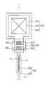
도 1은 본 발명의 실시예 1에 따른 모기판의 평면도이다. 도 2는 도 1에 도시된 모기판의 "A" 부분의 확대도이다.1 is a plan view of a mother board according to
도 1 및 도 2를 참조하면, 상기 모기판(200)은 복수의 표시 셀들(100a, 100b, 100c, 100d), 각 표시 셀(100a)을 정의하는 절단선(CL), 각 표시 셀(100a)에 대응하는 검사 패드부(TP) 및 신호 인입부(IP)를 포함한다.1 and 2, the
상기 표시 셀(100a)은 표시 영역(DA)과 상기 표시 영역(DA)을 둘러싸는 주변 영역들(PA1, PA2)을 포함한다. 상기 표시 영역(DA)에는 복수의 신호 배선들을 포함한다. 상기 신호 배선들은 복수의 데이트 배선들(DL), 복수의 게이트 배선들(GL), 복수의 스토리지 배선들(STL) 및 복수의 화소들(P)을 포함한다. 상기 데이터 배선들(DL)은 제1 방향으로 연장될 수 있다. 상기 게이트 배선들(GL)은 상기 제1 방향과 교차하는 제2 방향으로 연장될 수 있다. 상기 스토리지 배선들(STL)은 상기 제2 방향으로 연장될 수 있다. 각 화소(P)는 트랜지스터(TR) 및 상기 트랜지스터(TR)에 연결된 화소 전극(PE)을 포함한다.The
상기 제1 주변 영역(PA1)은 상기 게이트 배선들(GL)의 일단과 인접한 영역으로, 상기 게이트 배선들(GL)에 순차적으로 게이트 신호를 인가하는 게이트 구동회로(110)가 배치된다. 상기 게이트 구동회로(110)는 복수의 트랜지스터들을 포함하며, 상기 표시 영역(DA)에 배치된 상기 트랜지스터(TR)와 동일한 공정을 통해 상기 제1 주변 영역(PA1)에 형성된다.The first peripheral region PA1 is a region adjacent to one end of the gate lines GL and a
상기 제2 주변 영역(PA2)은 상기 데이터 배선들(DL)의 일단과 인접한 영역으로, 신호를 수신하는 패드부(130)가 배치된다. 상기 패드부(130)는 상기 데이터 배선들(DL), 상기 게이트 구동회로(110), 상기 스토리지 배선들(STL)에 제공되는 신호를 수신하는 복수의 패드들을 포함한다.The second peripheral area PA2 is an area adjacent to one end of the data lines DL, and a
상기 절단선(CL)은 상기 표시 셀(110a)을 정의하고, 후속 공정에서 상기 절 단선(CL)을 따라 상기 모기판을 절단한다.The cutting line CL defines the
상기 검사 패드부(TP)는 복수의 검사 패드들을 포함하고, 상기 표시 셀(100a)의 패드부(130)와 전기적으로 연결된다. 예를 들면, 상기 검사 패드부(TP)는 데이터 검사부(DT), 게이트 검사부(GT) 및 스토리지 검사부(ST)를 포함한다.The test pad unit TP includes a plurality of test pads and is electrically connected to the
상기 데이터 검사부(DT)는 상기 데이터 배선들(DL)의 불량을 검사하기 위한 검사신호를 수신한다. 데이터 검사 방식에 따라서 2개, 3개 등과 같이 복수의 데이터 검사패드들을 포함할 수 있다. 예를 들면, 2D 검사 방식에 따르면, 상기 데이터 배선들의 데이터 패드들을 제1 그룹 및 제2 그룹으로 나눈다. 상기 제1 그룹의 데이터 패드들은 제1 검사 패드(201)와 전기적으로 연결하고, 상기 제2 그룹의 데이터 패드들은 제2 검사 패드(202)와 전기적으로 연결한다. 상기 제1 그룹은 홀수 번째 데이터 패드들이고, 상기 제2 그룹은 짝수 번째 데이터 패드들일 수 있다.The data checking unit DT receives an inspection signal for inspecting the defects of the data lines DL. And may include a plurality of data check pads, such as two, three, etc. according to the data check method. For example, according to the 2D inspection scheme, the data pads of the data lines are divided into a first group and a second group. The first group of data pads are electrically connected to the
상기 게이트 검사부(GT)는 상기 게이트 배선들(GL)의 불량을 검사하기 위한 검사신호를 수신한다. 상기 게이트 검사부(GT)는 상기 게이트 구동회로(130)의 입력신호에 따라서 제3 검사 패드(203), 제4 검사 패드(204), 제5 검사 패드(205), 제6 검사 패드(206)를 포함할 수 있다. 상기 제3 검사 패드(203)는 상기 게이트 구동회로(110)의 수직개시신호를 수신하는 패드와 전기적으로 연결되고, 상기 제4 검사 패드(204)는 상기 게이트 구동회로(110)의 제1 클럭 신호를 수신하는 패드와 전적으로 연결되고, 상기 제5 검사 패드(205)는 상기 게이트 구동회로(110)의 제2 클럭 신호를 수신하는 패드와 전기적으로 연결되며, 상기 제6 검사 패드(206)는 상기 게이트 구동회로(110)의 게이트 오프전압을 수신하는 패드와 전기적으로 연결된다.The gate inspection unit GT receives an inspection signal for inspecting the defects of the gate lines GL. The gate inspecting unit GT includes a third inspecting
상기 스토리지 검사부(ST)는 상기 스토리지 배선들(GL)의 불량을 검사하기 위한 검사신호를 수신한다. 상기 스토리지 검사부(ST)는 상기 스토리지 배선들(STL)에 인가되는 스토리지 공통전압을 수신하는 제7 검사 패드(207)와 전기적으로 연결된다.The storage inspection unit ST receives an inspection signal for inspecting defects of the storage lines GL. The storage inspection unit ST is electrically connected to a
상기 신호 인입부(IP)는 상기 검사 패드부(TP)와 상기 절단선(CL) 사이에 배치되어 상기 검사 패드부(TP)로부터 수신된 검사신호를 상기 표시 셀(100a)의 상기 패드부(130)에 전달한다. 상기 신호 인입부(IP)는 상기 검사 패드부(TP)부터 상기 표시 셀(100a)의 상기 패드부(130)까지 연장된 복수의 연결 배선부들과 상기 검사 패드부(TP)와 상기 연결 배선부들을 전기적으로 연결하는 복수의 연결부들을 포함한다.The signal input unit IP is disposed between the test pad unit TP and the cut line CL and outputs an inspection signal received from the test pad unit TP to the
예를 들면, 제1 연결 배선부(211)는 상기 제1 검사 패드(201)로부터 연장되어 상기 패드부(130)에 연결되고, 상기 제2 연결 배선부(212)는 상기 제2 검사 패드(202)로부터 연장되어 상기 패드부(130)에 연결된다. 제3 연결 배선부(213)는 상기 제2 검사 패드(203)로부터 연장되어 상기 패드부(130)에 연결되고, 제4 연결 배선부(214)는 상기 제4 검사 패드(204)로부터 연장되어 상기 패드부(130)에 연결된다. 상기 제5 연결 배선부(215)는 상기 제5 검사 패드(205)로부터 연장되어 상기 패드부(130)에 연결되고, 제6 연결 배선부(216)는 상기 제6 검사 패드(206)로부터 연장되어 상기 패드부(130)에 연결되며, 제7 연결 배선부(217)는 상기 제7 검사 패드(207)로부터 연장되어 상기 패드부(130)에 연결된다.For example, the first
상기 제1 내지 제7 연결 배선부들(211, 212,.., 217) 각각은 정전기 차단패 턴(EBP)을 포함한다. 상기 정전기 차단패턴(EBP)은 각각의 검사 패드들(201, 202,...,207)과 인접한 위치에 배치된다. 상기 정전기 차단패턴(EBP)은 상기 검사 패드부(TP)로 인입된 정전기를 감소시켜 상기 정전기에 의해 상기 표시 셀(100a)이 손상되는 것을 방지한다.Each of the first to seventh
제1 연결부(221)는 상기 제1 검사 패드(201)와 상기 제1 연결 배선부(211)를 전기적으로 연결하고, 제2 연결부(222)는 상기 제2 검사 패드(202)와 상기 제2 연결 배선부(212)를 전기적으로 연결한다. 제3 연결부(223)는 상기 제3 검사 패드(203)와 상기 제3 연결 배선부(213)를 전기적으로 연결하고, 제4 연결부(224)는 상기 제4 검사 패드(204)와 상기 제4 연결 배선부(214)를 전기적으로 연결한다. 제5 연결 부(225)는 상기 제5 검사 패드(205)와 상기 제5 연결 배선부(215)를 전기적으로 연결하고, 제6 연결부(226)는 상기 제6 검사 패드(206)와 상기 제6 연결 배선부(216)를 전기적으로 연결하고, 제7 연결부(227)는 상기 제7 검사 패드(207)와 상기 제7 연결 배선부(217)를 전기적으로 연결한다.The
도 3은 도 2에 도시된 정전기 방지패턴을 설명하기 위한 평면도이다.3 is a plan view for explaining the antistatic pattern shown in FIG.
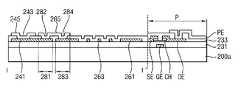
도 2 및 도 3을 참조하면, 상기 모기판(200)은 검사 패드(240), 연결 배선부(260) 및 연결부(280)를 포함한다. 상기 검사 패드(240), 상기 연결 배선부(260) 및 상기 연결부(280)는 도 2에 도시된 상기 검사 패드들(201,...,207), 상기 연결 배선부들(211,...,217) 및 상기 연결부들(221,...,227)을 대신하며, 이하에서는 상기 검사 패드(240), 상기 연결 배선부(260) 및 상기 연결부(280)를 통해 본 실시예를 보다 상세하게 설명한다.Referring to FIGS. 2 and 3, the
상기 검사 패드(240)는 제2 금속층으로 형성된 제1 패드전극(241)과 상기 제1 패드전극(241) 위에 형성된 제1 콘택홀(243) 및 투명 도전층으로 형성되고 상기 제1 콘택홀(243)을 통해 상기 제1 패드전극(241)과 연결되는 제2 패드전극(245)을 포함한다.The
상기 연결 배선부(260)는 상기 제2 금속층으로 형성된 연결 배선(261)과 정전기 방지패턴(263)을 포함한다. 상기 연결 배선(261)은 상기 정전기 방지패턴(263)으로부터 연장되어 상기 표시 셀(100a)의 패드부(130)와 전기적으로 연결된다. 상기 정전기 방지패턴(263)은 상기 연결 배선(261)과 전기적으로 연결되고, 상기 검사 패드(240) 측에 인접하게 배치된다. 상기 정전기 방지패턴(263)은 복수의 모서리들(E)로 이루어진 지그재그(zig-zag) 형상을 가진다.The
상기 연결부(280)는 상기 검사 패드(240)와 상기 연결 배선부(260)를 연결한다. 상기 연결부(280)는 상기 검사 패드(240)와 전기적으로 연결된 제1 단부(281)와 상기 제1 단부(281) 위에 형성된 제2 콘택홀(282)과 상기 연결 배선부(260)와 전기적으로 연결된 제2 단부(283)와 상기 제2 단부(283) 위에 형성된 제3 콘택홀(284) 및 상기 제2 및 제3 콘택홀들(282, 284)을 통해 상기 제1 및 제2 단부들(281, 283)을 연결하는 연결 전극(285)을 포함한다. 상기 제1 및 제2 단부들(281, 283)은 상기 제2 금속층으로 형성되고, 상기 연결 전극(285)은 상기 투명 도전층으로 형성될 수 있다.The
도시되지 않았으나, 상기 연결부(280)는 상기 제2 금속층으로 형성된 상기 제1 패드 전극(241)의 상기 제1 단부(281)를 연장하여 상기 제2 금속층으로 형성된 상기 연결 배선(261)과 직접 연결할 수 있다. 본 실시예와 같이, 상기 연결부(280)를 상기 제2 및 제3 콘택홀들(282, 284)을 통해 상기 투명 도전층으로 형성된 상기 연결 전극(285)으로 상기 제1 패드 전극(241)과 상기 연결 배선(261)을 간접적으로 연결함으로써 상기 정전기의 세기를 더욱 감소시킬 수 있다.Although not shown, the
어레이 검사 공정에서, 검사 장치의 프로브(probe)가 상기 검사 패드(240)에 접촉하는 순간 상기 프로브 끝단에 몰려 있는 정전기는 상기 검사 패드(240)를 통해 상기 표시 셀(100a)로 유입되게 된다. 상기 검사 패드(240)의 크기가 최소 2mm 로 다른 패턴에 비해 크기가 매우 크다. 따라서, 정전기 유입이 더 용이하다.In the array inspecting process, static electricity accumulated at the probe tip at the moment when a probe of the inspecting apparatus contacts the inspecting
이와 같이 상기 검사 패드(240)를 통해 상기 정전기가 인입되는 경우, 상기 정전기는 상기 지그재그 형상으로 형성된 상기 정전기 방지패턴(263)에 의해 세기가 점차적으로 감소된다. 일반적으로 상기 정전기는 배선의 모서리 등에서 더욱더 잘 터지는 성질이 있다. 따라서, 상기 정전기 방지패턴(263)에 의해 상기 표시 셀(100a) 내부로 유입되는 정전기의 크기는 감소되어, 상기 정전기에 의해 상기 표시 셀(100a)에 형성된 상기 게이트 구동회로(110) 및 상기 화소(P)의 트랜지스터(TR) 등이 상기 정전기에 의해 손상되는 것을 방지할 수 있다.When the static electricity is drawn through the
도 4a 내지 도 4c는 도 3에 도시된 정전기 방지패턴을 포함하는 모기판의 제조 방법을 설명하기 위한 단면도들이다.4A to 4C are cross-sectional views illustrating a method of manufacturing a mother board including the anti-static pattern shown in FIG.
도 2, 도 3 및 도 4a를 참조하면, 상기 모기판(200)은 베이스 기판(200a)을 포함한다. 상기 베이스 기판(200a)위에 제1 금속층을 형성하고, 상기 제1 금속층을 패터닝하여 제1 금속 패턴을 형성한다. 상기 제1 금속층은 단층 또는 다층 구조일 수 있다. 상기 제1 금속 패턴은 상기 표시 셀(100a)의 상기 게이트 배선들(GL), 상기 스토리지 배선들(STL), 상기 트랜지스터(TR)의 게이트 전극(GE)을 포함한다.2, 3 and 4A, the
상기 제1 금속 패턴이 형성된 상기 베이스 기판(200a) 위에 게이트 절연층(231)을 형성한다.A
도 2, 도 3 및 도 4b를 참조하면, 상기 게이트 절연층(231)이 형성된 상기 베이스 기판(200a) 위에 채널층을 형성하고, 상기 채널층을 패터닝하여 상기 트랜지스터(TR)의 채널패턴(CH)을 형성한다.2, 3, and 4B, a channel layer is formed on the
상기 채널 패턴(CH)이 형성된 상기 베이스 기판(200a) 위에 제2 금속층을 형성하고, 상기 제2 금속층을 패터닝하여 제2 금속 패턴을 형성한다. 상기 제2 금속층은 단층 또는 다층 구조일 수 있다. 상기 제2 금속 패턴은 상기 표시 셀(100a)의 상기 데이트 배선들(DL), 상기 트랜지스터(TR)의 소스 전극(SE) 및 드레인 전극(DE)을 포함한다. 또한, 상기 제2 금속 패턴은 상기 표시 셀(100a)의 주변 영역에 배치된 상기 제1 패드 전극(241), 상기 연결 배선(261), 정전기 방지패턴(263), 제1 단부(281) 및 제2 단부(283)를 포함한다. 상기 정전기 방지패턴(263)은 평면에서 관찰할 때, 지그재그 형상으로 형성된다.A second metal layer is formed on the
상기 제2 금속 패턴이 형성된 상기 베이스 기판(200a) 위에 보호층(233)을 형성한다.A
도 2, 도 3 및 도 4c를 참조하면, 상기 보호층(233)을 식각하여 상기 제2 금속 패턴을 노출시키는 상기 콘택홀들(243, 282, 284)을 형성한다.Referring to FIGS. 2, 3 and 4C, the
상기 콘택홀들(243, 282, 284)이 형성된 상기 베이스 기판(200a) 위에 투명 도전층을 형성하고, 상기 투명 도전층을 패터닝하여 투명 전극패턴을 형성한다. 상기 투명 전극패턴은 상기 표시 셀(100a)의 상기 화소 전극(PE), 상기 제2 패드 전극(245) 및 상기 연결 전극(285)을 포함한다.A transparent conductive layer is formed on the
이와 같이, 상기 정전기 방지패턴(263)은 기존 공정에서 상기 제2 금속층을 패터닝하는 마스크의 하나만 변형함으로써 간단하게 제조할 수 있다.As described above, the
이하에서는 실시예 1과 동일한 구성요소는 동일한 도면부호를 부여하고 반복되는 설명은 간략하게 한다. Hereinafter, the same components as those of the first embodiment will be denoted by the same reference numerals, and the repeated description will be simplified.
실시예 2Example 2
도 5는 본 발명의 실시예 2에 따른 정전기 방지패턴을 설명하기 위한 평면도이다.5 is a plan view for explaining an antistatic pattern according to a second embodiment of the present invention.
도 2 및 도 5를 참조하면, 상기 모기판은 검사 패드(240), 연결 배선부(360) 및 연결부(280)를 포함한다.Referring to FIGS. 2 and 5, the mother board includes an
상기 검사 패드(240)는 제1 패드전극(241)과 제1 콘택홀(243) 및 제2 패드전극(245)을 포함한다.The
상기 연결 배선부(360)는 제2 금속층을 형성된 연결 배선(261)과 정전기 방지패턴(363)을 포함한다. 상기 연결 배선(261)은 상기 정전기 방지패턴(363)으로부터 연장되어 상기 표시 셀(100a)의 패드부(130)와 전기적으로 연결된다. 상기 정전기 방지패턴(363)은 상기 연결 배선(261)과 전기적으로 연결되고, 상기 검사 패드(240) 측에 인접하게 배치된다. 상기 정전기 방지패턴(363)은 복수의 모서리들로 이루어지고, 배선 폭이 넓은 부분과 좁은 부분이 반복되는 구조를 가진다. 상기 넓은 부분의 폭(W1)은 제품의 종류에 따라서 다양하게 설정될 수 있으며, 상기 좁은 부분의 폭(W2)은 상기 넓은 부분의 폭(W1)의 1/2배 이하일 수 있다. 또는 상기 좁은 부분의 폭(W2)은 상기 넓은 부분의 폭(W1) 보다 약 1/5배 내지 1/2배 정도로 좁게 설정될 수 있다. 예를 들면, 상기 넓은 부분의 폭(W1)은 약 50 ㎛ 내지 30 ㎛ 정도이고, 상기 좁은 부분의 폭(W2)은 약 5 ㎛ 내지 15 ㎛ 정도이다. 10.1인치 제품의 경우, 상기 넓은 부분의 폭(W1)은 약 40 ㎛ 로, 상기 좁은 부분의 폭(W2)은 약 10 ㎛ 로 설정될 수 있다.The
일반적으로 정전기는 통로의 배선 폭이 변화할 때 세기가 감소하는 성질을 가진다. 이러한 점에서, 상기 정전기 방지패턴(363)은 배선 폭이 넓은 부분(W1)과 좁은 부분(W2)이 반복되는 구조를 가진다. 이에 의해 상기 정전기는 배선 폭이 넓은 부분(W1)에서 배선 폭이 좁은 부분(W2)으로 흐를 때, 또는 배선 폭이 좁은 부분(W2)에서 배선 폭이 넓은 부분(W1)으로 흐를 때 세기가 감소하고, 이러한 과정을 반복함으로써 상기 정전기 방지패턴(363)을 통과한 정전기의 세기는 현저히 감소하게 된다. 상기 좁은 부분의 폭(W2)이 상기 넓은 부분의 폭(W1)의 1/2보다 클 경우 정전기 방지가 효과적으로 이루어지지 않는다.Generally, static electricity has a property that intensity decreases when a width of a channel of a passage changes. In this regard, the
따라서, 상기 정전기에 의해 상기 표시 셀(100a)에 형성된 상기 게이트 구동회로(110) 및 상기 화소(P)의 트랜지스터(TR) 등이 상기 정전기에 의해 손상되는 것을 방지할 수 있다.Therefore, it is possible to prevent the
상기 연결부(280)는 제1 단부(281), 제2 콘택홀(282), 제2 단부(283), 제3 콘택홀(284) 및 연결 전극(285)을 포함한다. 상기 제1 및 제2 단부들(281, 283)은 상기 제2 금속층으로 형성되고, 상기 연결 전극(285)은 상기 투명 도전층으로 형성될 수 있다.The
본 실시예에 따른 모기판의 제조 방법은 도 4a 내지 도 4c를 참조하여 설명한 실시예 1에 따른 모기판이 제조 방법과 실질적으로 동일할 수 있다. 즉, 도 4c에 도시된 바와 같이, 상기 제2 금속층으로 배선 폭이 넓은 부분(W1)과 좁은 부분(W2)이 반복되는 구조의 상기 정전기 방지패턴(383)을 형성한다. 상기 정전기 방지패턴(383)의 평면상의 패턴 모양이 실시예 1과 다르고 이외의 제조 공정을 실질적으로 동일하므로 생략한다.The manufacturing method of the mother board according to the present embodiment may be substantially the same as the manufacturing method of the mother board according to the first embodiment described with reference to Figs. 4A to 4C. That is, as shown in FIG. 4C, the antistatic pattern 383 having a structure in which the portion W1 and the portion W2 having a wide wiring width are repeated in the second metal layer is formed. The shape of the pattern on the plane of the anti-static pattern 383 is different from that of the first embodiment, and the manufacturing steps other than the first embodiment are substantially the same.
이와 같이, 상기 정전기 방지패턴(363)은 기존 공정에서 상기 제2 금속층을 패터닝하는 마스크의 하나만 변형함으로써 간단하게 제조할 수 있다.As described above, the
실시예 3Example 3
도 6은 본 발명의 실시예 3에 따른 정전기 방지패턴을 설명하기 위한 평면도이다.6 is a plan view for explaining an antistatic pattern according to a third embodiment of the present invention.
도 2 및 도 6을 참조하면, 상기 모기판은 검사 패드(240), 연결 배선부(460) 및 연결부(280)를 포함한다.Referring to FIGS. 2 and 6, the mother board includes an
상기 검사 패드(240)는 제1 패드전극(241)과 제1 콘택홀(243) 및 제2 패드전극(245)을 포함한다.The
상기 연결 배선부(460)는 제2 금속층으로 형성된 연결 배선(261)과 제1 정전 기 방지패턴(263) 및 제2 정전기 방지패턴(363)을 포함한다. 상기 연결 배선(261)은 상기 제1 또는 제2 정전기 방지패턴(263 or 363)으로부터 연장되어 상기 표시 셀(100a)의 패드부(130)와 전기적으로 연결된다. 상기 제1 정전기 방지패턴(263)은 지그재그(zig-zag) 형상을 가진다. 상기 제2 정전기 방지패턴(363)은 상기 제1 정전기 방지패턴(263)과 인접하게 배치되고, 상대적으로 배선 폭이 넓은 부분(W1)과 좁은 부분(W2)이 반복되는 구조를 가진다.The
상기 제1 정전기 방지패턴(263)은 모서리 부분에서 상기 정전기를 감소시키고, 상기 제2 정전기 방지패턴(363)은 배선 폭이 변화되는 부분에서 상기 정전기를 감소시킨다. 상기 제1 및 제2 정전기 방지패턴들(263, 363)에 의해 상기 검사 패드(240)로 인입된 정전기는 현저히 감소할 수 있다. 따라서, 상기 정전기에 의해 상기 표시 셀(100a)에 형성된 상기 게이트 구동회로(110) 및 상기 화소(P)의 트랜지스터(TR) 등이 상기 정전기에 의해 손상되는 것을 방지할 수 있다.The first
상기 연결부(280)는 제1 단부(281), 제2 콘택홀(282), 제2 단부(283), 제3 콘택홀(284) 및 연결 전극(285)을 포함한다. 상기 제1 및 제2 단부들(281, 283)은 상기 제2 금속층으로 형성되고, 상기 연결 전극(285)은 상기 투명 도전층으로 형성될 수 있다.The
본 실시예에 따른 모기판의 제조 방법은 도 4a 내지 도 4c를 참조하여 설명한 실시예 1에 따른 모기판이 제조 방법과 실질적으로 동일할 수 있다. 즉, 도 4c에 도시된 바와 같이, 상기 제2 금속층으로 상기 제1 정전기 방지패턴(283) 및 제2 정전기 방지패턴(383)을 형성한다.The manufacturing method of the mother board according to the present embodiment may be substantially the same as the manufacturing method of the mother board according to the first embodiment described with reference to Figs. 4A to 4C. That is, as shown in FIG. 4C, the first
이와 같이, 상기 제1 및 제2 정전기 방지패턴들(263, 363)은 기존 공정에서 상기 제2 금속층을 패터닝하는 마스크의 하나만 변형함으로써 간단하게 제조할 수 있다.Thus, the first and second
실시예 4Example 4
도 7은 본 발명의 실시예 4에 따른 정전기 방지패턴을 설명하기 위한 평면도이다.7 is a plan view for explaining an antistatic pattern according to a fourth embodiment of the present invention.
도 2 및 도 7을 참조하면, 모기판은 검사 패드(240), 연결 배선부(560) 및 연결부(280)를 포함한다.Referring to FIGS. 2 and 7, the mother board includes an
상기 검사 패드(240)는 제1 패드전극(241)과 제1 콘택홀(243) 및 제2 패드전극(245)을 포함한다.The
상기 연결 배선부(560)는 연결 배선(261) 및 정전기 방지패턴(563)을 포함한다.The
상기 연결 배선(261)은 제2 금속층으로 형성된다. 상기 정전기 방지패턴(563)은 제1 금속층으로 형성된 제1 방지패턴(563a)과 상기 제2 금속층으로 형성된 제2 방지패턴(563b)을 포함한다. 상기 제1 방지패턴(563a)은 불연속적으로 배치된 복수의 패턴들(D)을 포함하는 사다리 형상을 가지고 상기 제2 방지패턴(563b)은 상기 제1 방지패턴(563a) 위에 중첩되고 복수의 단차들을 포함한다. 상기 연결 배선(261)은 상기 정전기 방지패턴(563)의 상기 제2 방지패턴(563b)으로부터 연장되어 상기 표시 셀(100a)의 패드부(130)와 전기적으로 연결된다.The
상기 연결부(280)는 제1 단부(281), 제2 콘택홀(282), 제2 단부(283), 제3 콘택홀(284) 및 연결 전극(285)을 포함한다. 상기 제1 및 제2 단부들(281, 283)은 상기 제2 금속층으로 형성되고, 상기 연결 전극(285)은 상기 투명 도전층으로 형성될 수 있다.The
상기 검사 패드(240)에 수신된 검사 신호는 상기 연결부(280)를 통해 상기 연결 배선부(560)에 전달되고, 상기 연결부(280)의 제2 단부(283)로부터 연장된 상기 제2 방지패턴(563b) 및 상기 연결 배선(261)을 상기 표시 셀(100a)의 패드부(130)에 전달된다. 한편, 상기 검사 패드(240)로부터 인입된 정전기는 상기 제2 방지패턴(563b)을 통해 흐른다. 이 경우, 상기 제2 방지패턴(563b)은 아래에 배치된 상기 사다리 형상의 상기 제1 방지패턴(563a)에 의해 복수의 단차들을 가진다. 상기 단차들 각각의 높이는 상기 제1 방지패턴(563a)의 두께에 기초한다. 상기 제1 방지패턴(533a)의 두께는 약 0.2 ㎛ 내지 0.3 ㎛ 정도 이므로, 상기 단차의 높이는 약 0.2 ㎛ 내지 0.3 ㎛ 정도를 가질 수 있다.The inspection signal received at the
상기 제2 방지패턴(563b)에 흐르는 상기 정전기는 단차가 바뀌는 지점에서 감소된다. 따라서, 상기 정전기에 의해 상기 표시 셀(100a)에 형성된 상기 게이트 구동회로(110) 및 상기 화소(P)의 트랜지스터(TR) 등이 상기 정전기에 의해 손상되는 것을 방지할 수 있다.The static electricity flowing in the
도 8a 내지 도 8c는 도 7에 도시된 정전기 방지패턴을 포함하는 모기판의 제조 방법을 설명하기 위한 단면도들이다.8A to 8C are cross-sectional views illustrating a method of manufacturing a mother board including the antistatic pattern shown in FIG.
도 7 및 도 8a를 참조하면, 상기 모기판은 베이스 기판(200a)을 포함한다. 상기 베이스 기판(200a)위에 제1 금속층을 형성하고, 상기 제1 금속층을 패터닝하여 제1 금속 패턴을 형성한다. 상기 제1 금속층은 약 0.2 ㎛ 내지 0.3 ㎛ 정도의 두께로 형성되며, 이에 따라서, 상기 제1 금속 패턴은 약 0.2 ㎛ 내지 0.3 ㎛ 정도의 두께를 가진다.Referring to FIGS. 7 and 8A, the mother substrate includes a
상기 제1 금속 패턴은 상기 표시 셀(100a)의 상기 게이트 배선들(GL), 상기 스토리지 배선들(STL), 상기 트랜지스터(TR)의 게이트 전극(GE)을 포함한다. 상기 제1 금속 패턴은 불연속적으로 배치된 복수의 패턴들(D)을 포함하는 제1 방지패턴(563a)을 포함한다. 상기 제1 방지패턴(563a)은 평면상에서 관찰할 때, 사다리 형상을 가진다.The first metal pattern includes the gate lines GL of the
상기 제1 금속 패턴이 형성된 상기 베이스 기판(200a) 위에 게이트 절연층(231)을 형성한다.A
도 7 및 도 8b를 참조하면, 상기 게이트 절연층(231)이 형성된 상기 베이스 기판(200a) 위에 채널층을 형성하고, 상기 채널층을 패터닝하여 상기 트랜지스터(TR)의 채널패턴(CH)을 형성한다.7 and 8B, a channel layer is formed on the
상기 채널패턴(CH)이 형성된 상기 베이스 기판(200a) 위에 제2 금속층을 형성하고, 상기 제2 금속층을 패터닝하여 제2 금속 패턴을 형성한다. 상기 제2 금속층은 약 0.2 ㎛ 내지 0.3 ㎛ 정도의 두께로 형성되며, 이에 따라서, 상기 제2 금속 패턴은 약 0.2 ㎛ 내지 0.3 ㎛ 정도의 두께를 가진다.A second metal layer is formed on the
상기 제2 금속 패턴은 상기 표시 셀(100a)의 상기 데이트 배선들(DL), 상기 트랜지스터(TR)의 소스 전극(SE) 및 드레인 전극(DE)을 포함한다. 또한, 상기 제2 금속 패턴을 상기 표시 셀(100a)의 주변 영역에 배치된 상기 제1 패드 전극(241), 상기 연결 배선(261), 상기 정전기 방지패턴(563)의 제2 방지패턴(563b), 제1 단부(281) 및 제2 단부(283)를 포함한다. 상기 제2 방지패턴(563b)은 상기 제2 단부(283)로부터 연장되어 상기 연결 배선(261)과 연결된다. 상기 제2 방지패턴(563b)은 상기 불연속적으로 배치된 복수의 패턴들(D)을 포함하는 상기 제1 방지패턴(563a)위에 중첩되어 형성되고, 상기 복수의 패턴들(D)에 의해 복수의 단차들(S)을 포함한다. 상기 단차들(S) 각각의 높이(h)는 상기 제1 방지패턴(563a)의 두께에 기초한다. 즉, 상기 제1 방지패턴(563a)의 두께가 약 0.2 ㎛ 내지 0.3 ㎛ 정도이므로, 상기 각 단차의 높이(h)는 약 0.2 ㎛ 내지 0.3 ㎛ 정도이다. 상기 제2 방지 패턴(563b)에 인가된 상기 정전기는 상기 제2 방지패턴(563b)의 단차들(S)을 통과할 때 감쇄될 수 있다.The second metal pattern includes the data lines DL of the
상기 제2 금속 패턴이 형성된 상기 베이스 기판(200a) 위에 보호층(233)을 형성한다.A
도 7 및 도 8c를 참조하면, 상기 보호층(233)을 식각하여 상기 제2 금속 패턴을 노출시키는 상기 콘택홀들(243, 282, 284)을 형성한다.Referring to FIGS. 7 and 8C, the
상기 콘택홀들(243, 282, 284)이 형성된 상기 베이스 기판(200a) 위에 투명 도전층을 형성하고, 상기 투명 도전층을 패터닝하여 투명 전극패턴을 형성한다. 상기 투명 전극패턴은 상기 표시 셀(100a)의 상기 화소 전극(PE), 상기 제2 패드 전극(245) 및 상기 연결 전극(285)을 포함한다.A transparent conductive layer is formed on the
이와 같이, 본 실시예에 따른 상기 정전기 방지패턴(563)은 제2 방지패턴에 단차를 형성하기 위해 제1 방지패턴을 추가적으로 형성하는 것으로, 상기 제1 금속층을 패터닝하는 마스크 하나만 변형함으로써 간단하게 제조할 수 있다.As described above, the
실시예 5Example 5
도 9는 본 발명의 실시예 5에 따른 정전기 방지패턴을 설명하기 위한 평면도이다.9 is a plan view for explaining an antistatic pattern according to a fifth embodiment of the present invention.
도 2 및 도 7을 참조하면, 모기판은 검사 패드(240), 연결 배선부(660) 및 연결부(280)를 포함한다.2 and 7, the mother board includes an
상기 검사 패드(240)는 제1 패드전극(241)과 제1 콘택홀(243) 및 제2 패드전극(245)을 포함한다.The
상기 연결 배선부(660)는 연결 배선(261) 및 정전기 방지패턴(663)을 포함한다. 상기 연결 배선(261)은 제2 금속층으로 형성된다. 상기 정전기 방지패턴(663)은 제1 금속층으로 형성된 제1 방지패턴(663a)과 상기 제2 금속층으로 형성된 제2 방지패턴(663b)을 포함한다. 상기 제1 방지패턴(663a)은 불연속적으로 배치된 복수의 패턴들(D)을 포함하는 징검다리 형상을 가지고, 상기 제2 방지패턴(663b)은 상기 제1 방지패턴(663a) 위에 중첩되어 복수의 단차들을 포함한다. 상기 연결 배선(261)은 상기 정전기 방지패턴(663)의 상기 제2 방지패턴(663b)으로부터 연장되어 상기 표시 셀(100a)의 패드부(130)와 전기적으로 연결된다.The
상기 연결부(280)는 제1 단부(281), 제2 콘택홀(282), 제2 단부(283), 제3 콘택홀(284) 및 연결 전극(285)을 포함한다. 상기 제1 및 제2 단부들(281, 283)은 상기 제2 금속층으로 형성되고, 상기 연결 전극(285)은 상기 투명 도전층으로 형성될 수 있다.The
상기 검사 패드(240)에 수신된 검사 신호는 상기 연결부(280)를 통해 상기 연결 배선부(660)에 전달되고, 상기 연결부(280)의 제2 단부(283)로부터 연장된 상기 제2 방지패턴(663b) 및 상기 연결 배선(261)을 상기 표시 셀(100a)의 패드부(130)에 전달된다. 한편, 상기 검사 패드(240)로부터 인입된 정전기는 상기 제2 방지패턴(663b)을 통해 흐른다. 이 경우, 상기 제2 방지패턴(663b)은 아래에 배치된 상기 징검다리 형상의 상기 제1 방지패턴(663a)에 의해 복수의 단차들을 가진다. 상기 제2 방지패턴(663b)에 흐르는 상기 정전기는 단차가 바뀌는 지점에서 감소된다. 따라서, 상기 정전기에 의해 상기 표시 셀(100a)에 형성된 상기 게이트 구동회로(110) 및 상기 화소(P)의 트랜지스터(TR) 등이 상기 정전기에 의해 손상되는 것을 방지할 수 있다.The inspection signal received at the
본 실시예에 따른 모기판의 제조 방법은 도 8a 내지 도 8c를 참조하여 설명한 실시예 4에 따른 모기판이 제조 방법과 실질적으로 동일할 수 있다. 즉, 도 8a에 도시된 바와 같이, 상기 제2 방지패턴(663b)이 형성되는 영역에 대응하여 상기 제1 금속층으로 징검다리 형상의 상기 제1 방지패턴(663a)을 형성한다. 이에 의해 도 8b를 참조하면, 상기 제2 금속층으로 형성된 상기 제2 방지패턴(663b)은 복수의 단차들(S)을 포함할 수 있다. The manufacturing method of the mother board according to this embodiment may be substantially the same as the manufacturing method of the mother board according to the fourth embodiment described with reference to Figs. 8A to 8C. That is, as shown in FIG. 8A, the
이와 같이, 상기 정전기 방지패턴(663)은 제2 방지패턴에 단차를 형성하기 위해 상기 제1 방지패턴을 추가적으로 형성하는 것으로, 상기 제1 금속층을 패터닝 하는 마스크 하나만 변형함으로써 간단하게 제조할 수 있다.As described above, the
실시예 6Example 6
도 10은 본 발명의 실시예 6에 따른 정전기 방지패턴을 설명하기 위한 평면도이다.10 is a plan view for explaining an antistatic pattern according to a sixth embodiment of the present invention.
도 2 및 도 10을 참조하면, 모기판은 검사 패드(240), 연결 배선부(760) 및 연결부(280)를 포함한다.Referring to FIGS. 2 and 10, the mother board includes a
상기 검사 패드(240)는 제1 패드전극(241)과 제1 콘택홀(243) 및 제2 패드전극(245)을 포함한다.The
상기 연결 배선부(760)는 연결 배선(261), 제1 정전기 방지패턴(663) 및 제2 정전기 방지패턴(563)을 포함한다. 상기 연결 배선(261)은 제2 금속층으로 형성된다. 상기 제1 정전기 방지패턴(663)은 제1 금속층으로 형성된 제1 방지패턴(663a)과 상기 제2 금속층으로 형성된 제2 방지패턴(663b)을 포함한다. 상기 제1 방지패턴(663a)은 징검다리 형상을 가지고 상기 제2 방지패턴(663b)은 상기 제1 방지패턴(663a) 위에 중첩되도록 배치된다. 상기 제2 정전기 방지패턴(563)은 상기 제1 금속층으로 형성된 제3 방지패턴(563a)과 제2 금속층으로 형성된 제4 방지패턴(563b)을 포함한다. 상기 제3 방지패턴(563a)은 사다리 형상을 가지고 상기 제4 방지패턴(563b)은 상기 제1 방지패턴(563a) 위에 중첩되도록 배치된다. 상기 연결 배선(261)은 상기 제2 또는 제4 방지패턴(663b, 563b)으로부터 연장되어 상기 표시 셀(100a)의 패드부(130)와 전기적으로 연결된다.The
상기 연결부(280)는 제1 단부(281), 제2 콘택홀(282), 제2 단부(283), 제3 콘택홀(284) 및 연결 전극(285)을 포함한다. 상기 제1 및 제2 단부들(281, 283)은 상기 제1 금속층으로 형성되고, 상기 연결 전극(285)은 상기 투명 도전층으로 형성될 수 있다.The
상기 검사 패드(240)로부터 인입된 정전기는 상기 제2 방지패턴(663b)을 통해 흐른다. 이 경우, 상기 제2 방지패턴(663b)은 아래에 배치된 상기 징검다리 형상의 상기 제1 방지패턴(663a)에 의해 복수의 단차들을 가진다. 상기 제2 방지패턴(663b)에 흐르는 상기 정전기는 단차가 바뀌는 지점에서 감소된다. 또한, 상기 정전기는 상기 제4 방지패턴(563b)을 통해 흐른다. 상기 제4 방지패턴(563b)은 아래에 배치된 상기 사다리 형상의 상기 제3 방지패턴(563a)에 의해 복수의 단차들을 가진다. 상기 제4 방지패턴(563b)에 흐르는 상기 정전기는 단차가 바뀌는 지점에서 감소된다.The static electricity drawn from the
따라서, 상기 제1 및 제2 정전기 방지패턴들(663, 563)에 의해 상기 표시 셀(100a)에 형성된 상기 게이트 구동회로(110) 및 상기 화소(P)의 트랜지스터(TR) 등이 상기 정전기에 의해 손상되는 것을 방지할 수 있다.Therefore, the
본 실시예에 따른 모기판의 제조 방법은 도 8a 내지 도 8c를 참조하여 설명한 실시예 4에 따른 모기판이 제조 방법과 실질적으로 동일할 수 있다. 즉, 도 8a에 도시된 바와 같이, 상기 제2 및 제4 방지패턴들(663b, 563b)이 형성되는 영역에 대응하여 상기 제1 금속층으로 사다리 형상 및 징검다리 형상의 상기 제1 및 제3 방지패턴들(663a, 563a)을 형성한다. 이에 의해 도 8b를 참조하면, 상기 제2 금속 층으로 형성된 상기 제2 및 제4 방지패턴들(663b, 563b)은 복수의 단차들(S)을 포함할 수 있다.The manufacturing method of the mother board according to this embodiment may be substantially the same as the manufacturing method of the mother board according to the fourth embodiment described with reference to Figs. 8A to 8C. That is, as shown in FIG. 8A, the first and third protection layers 663b and 563b are formed in the first and second metal layers so as to correspond to the regions where the second and
이와 같이, 상기 제1 및 제2 정전기 방지패턴들(663, 563)은 제2 및 제4 방지패턴에 단차를 형성하기 위해 상기 제1 및 제3 방지패턴을 추가적으로 형성하는 것으로, 상기 제1 금속층을 패터닝하는 마스크 하나만 변형함으로써 간단하게 제조할 수 있다.As described above, the first and second
이상에서는 실시예들을 참조하여 설명하였지만, 해당 기술 분야의 숙련된 당업자는 하기의 특허 청구의 범위에 기재된 본 발명의 사상 및 영역으로부터 벗어나지 않는 범위 내에서 본 발명을 다양하게 수정 및 변경시킬 수 있음을 이해할 수 있을 것이다.It will be apparent to those skilled in the art that various modifications and variations can be made in the present invention without departing from the spirit or scope of the present invention as defined by the following claims. You will understand.
도 1은 본 발명의 실시예 1에 따른 모기판의 평면도이다.1 is a plan view of a mother board according to
도 2는 도 1에 도시된 모기판의 "A" 부분의 확대도이다.2 is an enlarged view of the "A" portion of the mother board shown in Fig.
도 3은 도 2에 도시된 정전기 방지패턴을 설명하기 위한 평면도이다.3 is a plan view for explaining the antistatic pattern shown in FIG.
도 4a 내지 도 4c는 도 3에 도시된 정전기 방지패턴을 포함하는 모기판의 제조 방법을 설명하기 위한 단면도들이다.4A to 4C are cross-sectional views illustrating a method of manufacturing a mother board including the anti-static pattern shown in FIG.
도 5는 본 발명의 실시예 2에 따른 정전기 방지패턴을 설명하기 위한 평면도이다.5 is a plan view for explaining an antistatic pattern according to a second embodiment of the present invention.
도 6은 본 발명의 실시예 3에 따른 정전기 방지패턴을 설명하기 위한 평면도이다.6 is a plan view for explaining an antistatic pattern according to a third embodiment of the present invention.
도 7은 본 발명의 실시예 4에 따른 정전기 방지패턴을 설명하기 위한 평면도이다.7 is a plan view for explaining an antistatic pattern according to a fourth embodiment of the present invention.
도 8a 내지 도 8c는 도 7에 도시된 정전기 방지패턴을 포함하는 모기판의 제조 방법을 설명하기 위한 단면도들이다.8A to 8C are cross-sectional views illustrating a method of manufacturing a mother board including the antistatic pattern shown in FIG.
도 9는 본 발명의 실시예 5에 따른 정전기 방지패턴을 설명하기 위한 평면도이다.9 is a plan view for explaining an antistatic pattern according to a fifth embodiment of the present invention.
도 10은 본 발명의 실시예 6에 따른 정전기 방지패턴을 설명하기 위한 평면도이다.10 is a plan view for explaining an antistatic pattern according to a sixth embodiment of the present invention.
<도면의 주요부분에 대한 부호의 설명>Description of the Related Art
200 : 모기판CL : 절단선200: mother board CL: cutting line
100a, 100b, 100c, 100d, 100e, 100f : 표시 셀100a, 100b, 100c, 100d, 100e, 100f:
201, 202, 203, 204, 205, 206, 207, 240 : 검사 패드201, 202, 203, 204, 205, 206, 207, 240:
221, 222,223, 224, 225, 226, 227, 280 : 연결부221, 222, 223, 224, 225, 226, 227, 280:
EBP, 263, 363, 563, 663 : 정전기 방지패턴EBP, 263, 363, 563, 663: Antistatic pattern
260, 360, 460, 560, 660, 760 : 연결 배선부260, 360, 460, 560, 660, 760:
Claims (23)
Translated fromKoreanPriority Applications (3)
| Application Number | Priority Date | Filing Date | Title |
|---|---|---|---|
| KR1020090101528AKR101587936B1 (en) | 2009-10-26 | 2009-10-26 | Mother substrate for display device and method for manufacturing the same |
| US12/727,885US8520158B2 (en) | 2009-10-26 | 2010-03-19 | Substrate for a display device and method of manufacturing the same |
| US13/938,541US8854564B2 (en) | 2009-10-26 | 2013-07-10 | Substrate for a display device and method of manufacturing the same |
Applications Claiming Priority (1)
| Application Number | Priority Date | Filing Date | Title |
|---|---|---|---|
| KR1020090101528AKR101587936B1 (en) | 2009-10-26 | 2009-10-26 | Mother substrate for display device and method for manufacturing the same |
Publications (2)
| Publication Number | Publication Date |
|---|---|
| KR20110045119A KR20110045119A (en) | 2011-05-04 |
| KR101587936B1true KR101587936B1 (en) | 2016-01-25 |
Family
ID=43898246
Family Applications (1)
| Application Number | Title | Priority Date | Filing Date |
|---|---|---|---|
| KR1020090101528AActiveKR101587936B1 (en) | 2009-10-26 | 2009-10-26 | Mother substrate for display device and method for manufacturing the same |
Country Status (2)
| Country | Link |
|---|---|
| US (2) | US8520158B2 (en) |
| KR (1) | KR101587936B1 (en) |
Families Citing this family (23)
| Publication number | Priority date | Publication date | Assignee | Title |
|---|---|---|---|---|
| US8325315B2 (en)* | 2008-08-19 | 2012-12-04 | Samsung Display Co., Ltd. | Mother panel and method of manufacturing display panel using the same |
| TW201327312A (en)* | 2011-12-19 | 2013-07-01 | Wintek Corp | Touch panel having electrostatic protecting structure |
| KR102145390B1 (en) | 2013-10-25 | 2020-08-19 | 삼성디스플레이 주식회사 | Display device including electrostatic discharge circuit |
| KR20150059946A (en)* | 2013-11-25 | 2015-06-03 | 삼성디스플레이 주식회사 | Liquid crystal display and and manufacturing method therrof |
| CN103728804B (en)* | 2013-12-27 | 2016-02-24 | 京东方科技集团股份有限公司 | A kind of motherboard, array base palte and preparation method, display device |
| CN104035217B (en)* | 2014-05-21 | 2016-08-24 | 深圳市华星光电技术有限公司 | The peripheral test circuit of display array substrate and display panels |
| CN104020593A (en)* | 2014-05-30 | 2014-09-03 | 深圳市华星光电技术有限公司 | Array substrate, manufacturing method and liquid crystal display panel |
| CN104181717B (en)* | 2014-09-02 | 2017-04-19 | 深圳市华星光电技术有限公司 | Test unit for array substrates, array substrate and display device |
| CN104345484B (en)* | 2014-11-04 | 2017-03-29 | 京东方科技集团股份有限公司 | Test cell, array base palte and its manufacture method, display floater and display device |
| KR102272479B1 (en)* | 2014-12-09 | 2021-07-02 | 삼성디스플레이 주식회사 | Display device |
| KR102440559B1 (en)* | 2015-06-03 | 2022-09-06 | 삼성디스플레이 주식회사 | Liquid crystal display device and manufacturing method of liquid crystal display device |
| KR20170080851A (en)* | 2015-12-30 | 2017-07-11 | 삼성디스플레이 주식회사 | Display apparatus and method of driving the same |
| US10558101B2 (en) | 2016-03-22 | 2020-02-11 | Boe Technology Group Co., Ltd. | Array substrate motherboard, display panel motherboard, and fabricating method thereof |
| CN105607316B (en)* | 2016-03-22 | 2018-12-18 | 京东方科技集团股份有限公司 | A kind of array substrate motherboard and display panel motherboard |
| KR102542604B1 (en) | 2018-04-03 | 2023-06-15 | 삼성디스플레이 주식회사 | Organic light emitting display device and testing method of the same |
| CN109801909B (en)* | 2018-06-12 | 2024-08-20 | 京东方科技集团股份有限公司 | Array substrate mother board and manufacturing method thereof, array substrate and display device |
| CN109031723B (en)* | 2018-08-22 | 2021-06-04 | 惠科股份有限公司 | Array substrate, liquid crystal module and liquid crystal display equipment |
| CN108873441A (en)* | 2018-09-03 | 2018-11-23 | 深圳市宇顺电子股份有限公司 | A kind of LCD antistatic line |
| CN109786373A (en)* | 2018-12-26 | 2019-05-21 | 友达光电(昆山)有限公司 | Display panel |
| CN109935583B (en)* | 2019-03-28 | 2021-03-02 | 京东方科技集团股份有限公司 | Array substrate, display panel and manufacturing method of array substrate |
| CN110703520B (en)* | 2019-09-17 | 2020-11-24 | 深圳市华星光电半导体显示技术有限公司 | Display panel mother board, manufacturing method thereof and display panel |
| CN111653548A (en) | 2020-06-18 | 2020-09-11 | 京东方科技集团股份有限公司 | A display substrate, a display panel and a preparation method thereof |
| CN115312513A (en)* | 2022-07-28 | 2022-11-08 | 云谷(固安)科技有限公司 | Display panels and electronic equipment |
Citations (2)
| Publication number | Priority date | Publication date | Assignee | Title |
|---|---|---|---|---|
| KR100294684B1 (en) | 1998-04-25 | 2001-07-12 | 구본준, 론 위라하디락사 | Aparature for preventing a static electricity of Liquid Crystal Display for a Chip on Glass |
| KR100749482B1 (en) | 2004-06-17 | 2007-08-14 | 삼성에스디아이 주식회사 | LCD with antistatic structure |
Family Cites Families (10)
| Publication number | Priority date | Publication date | Assignee | Title |
|---|---|---|---|---|
| JPH09203908A (en)* | 1996-01-25 | 1997-08-05 | Furontetsuku:Kk | Thin-film transistor for liquid crystal display device and liquid crystal display device |
| JP3006584B2 (en)* | 1998-05-14 | 2000-02-07 | 日本電気株式会社 | Thin film transistor array |
| TW457690B (en)* | 1999-08-31 | 2001-10-01 | Fujitsu Ltd | Liquid crystal display |
| JP4006304B2 (en)* | 2002-09-10 | 2007-11-14 | 株式会社 日立ディスプレイズ | Image display device |
| KR100878242B1 (en)* | 2002-10-14 | 2009-01-13 | 삼성전자주식회사 | Thin film transistor array substrate and manufacturing method thereof |
| US7868957B2 (en)* | 2003-12-02 | 2011-01-11 | Semiconductor Energy Laboratory Co., Ltd. | Thin film transistor, display device and liquid crystal display device and method for manufacturing the same |
| KR100847640B1 (en)* | 2006-05-23 | 2008-07-21 | 가시오게산키 가부시키가이샤 | Display device |
| KR20080000097A (en)* | 2006-06-26 | 2008-01-02 | 삼성전자주식회사 | Array substrate and display device having same |
| KR101306860B1 (en)* | 2006-11-07 | 2013-09-10 | 삼성디스플레이 주식회사 | Display device and method for manufacturing the same |
| KR101033463B1 (en)* | 2008-06-13 | 2011-05-09 | 엘지디스플레이 주식회사 | Array Board for Liquid Crystal Display |
- 2009
- 2009-10-26KRKR1020090101528Apatent/KR101587936B1/enactiveActive
- 2010
- 2010-03-19USUS12/727,885patent/US8520158B2/enactiveActive
- 2013
- 2013-07-10USUS13/938,541patent/US8854564B2/enactiveActive
Patent Citations (2)
| Publication number | Priority date | Publication date | Assignee | Title |
|---|---|---|---|---|
| KR100294684B1 (en) | 1998-04-25 | 2001-07-12 | 구본준, 론 위라하디락사 | Aparature for preventing a static electricity of Liquid Crystal Display for a Chip on Glass |
| KR100749482B1 (en) | 2004-06-17 | 2007-08-14 | 삼성에스디아이 주식회사 | LCD with antistatic structure |
Also Published As
| Publication number | Publication date |
|---|---|
| US20130294004A1 (en) | 2013-11-07 |
| US20110096449A1 (en) | 2011-04-28 |
| US8854564B2 (en) | 2014-10-07 |
| US8520158B2 (en) | 2013-08-27 |
| KR20110045119A (en) | 2011-05-04 |
Similar Documents
| Publication | Publication Date | Title |
|---|---|---|
| KR101587936B1 (en) | Mother substrate for display device and method for manufacturing the same | |
| KR101579853B1 (en) | A display panel having an anti-static pattern | |
| KR101051012B1 (en) | Display panel mother substrate and manufacturing method thereof | |
| KR101614900B1 (en) | Display panel | |
| KR101591476B1 (en) | DISPLAY SUBSTRATE, METHOD FOR MANUFACTURING SAME | |
| KR101571768B1 (en) | DISPLAY SUBSTRATE, MISUSE REPAIR METHOD OF THE SAME, AND MOTHER PLATE WITH THE DISPLAY SUBSTRATE | |
| CN100492142C (en) | Array substrate and manufacturing method thereof | |
| KR101635858B1 (en) | Display substrate and method of manufacturing the sam | |
| KR20170139702A (en) | Flexible organic light emitting diode display device | |
| CN116072023B (en) | Display panel and display device | |
| KR20070002278A (en) | Display substrate and display device having same | |
| JP5053479B2 (en) | Matrix array substrate and manufacturing method thereof | |
| CN100405882C (en) | Mounting structures, substrates for mounting, electro-optical devices, and electronic instruments | |
| KR101137863B1 (en) | Thin Film Transistor Array Substrate | |
| KR100490040B1 (en) | Liquid crystal display device with two or more shorting bars and method for manufacturing same | |
| KR100806885B1 (en) | Manufacturing Method Of Liquid Crystal Display | |
| KR101889439B1 (en) | Liquid Crystal Display Device, Photo Mask for Liquid Crystal Display and Method of fabricating Liquid Crystal Display Device | |
| KR100943284B1 (en) | Pad structure in chip-on-glass mounted LCD | |
| JPH07318980A (en) | Liquid crystal display panel | |
| KR101354317B1 (en) | Display device having electrostatic protection structure | |
| CN113823643A (en) | Array substrate motherboard, array substrate, display panel and display device | |
| KR101035177B1 (en) | Array substrate of liquid crystal display device and manufacturing method thereof | |
| KR100455860B1 (en) | Probe Pad on LCD Panel | |
| KR20080044398A (en) | Array substrate and method for manufacturing same | |
| KR20050108886A (en) | Mother board having array substrate for display panel |
Legal Events
| Date | Code | Title | Description |
|---|---|---|---|
| PA0109 | Patent application | Patent event code:PA01091R01D Comment text:Patent Application Patent event date:20091026 | |
| PG1501 | Laying open of application | ||
| N231 | Notification of change of applicant | ||
| PN2301 | Change of applicant | Patent event date:20120913 Comment text:Notification of Change of Applicant Patent event code:PN23011R01D | |
| A201 | Request for examination | ||
| PA0201 | Request for examination | Patent event code:PA02012R01D Patent event date:20140901 Comment text:Request for Examination of Application Patent event code:PA02011R01I Patent event date:20091026 Comment text:Patent Application | |
| E902 | Notification of reason for refusal | ||
| PE0902 | Notice of grounds for rejection | Comment text:Notification of reason for refusal Patent event date:20150430 Patent event code:PE09021S01D | |
| E701 | Decision to grant or registration of patent right | ||
| PE0701 | Decision of registration | Patent event code:PE07011S01D Comment text:Decision to Grant Registration Patent event date:20151029 | |
| GRNT | Written decision to grant | ||
| PR0701 | Registration of establishment | Comment text:Registration of Establishment Patent event date:20160118 Patent event code:PR07011E01D | |
| PR1002 | Payment of registration fee | Payment date:20160119 End annual number:3 Start annual number:1 | |
| PG1601 | Publication of registration | ||
| FPAY | Annual fee payment | Payment date:20190102 Year of fee payment:4 | |
| PR1001 | Payment of annual fee | Payment date:20190102 Start annual number:4 End annual number:4 | |
| FPAY | Annual fee payment | Payment date:20191223 Year of fee payment:5 | |
| PR1001 | Payment of annual fee | Payment date:20191223 Start annual number:5 End annual number:5 | |
| PR1001 | Payment of annual fee | Payment date:20210104 Start annual number:6 End annual number:6 | |
| PR1001 | Payment of annual fee | Payment date:20211228 Start annual number:7 End annual number:7 | |
| PR1001 | Payment of annual fee | Payment date:20221226 Start annual number:8 End annual number:8 | |
| PR1001 | Payment of annual fee | Payment date:20241230 Start annual number:10 End annual number:10 |