KR101579839B1 - Output Buffer Having High Slew Rate, Output Buffer Control Method, and Display Driver Having It - Google Patents
Output Buffer Having High Slew Rate, Output Buffer Control Method, and Display Driver Having ItDownload PDFInfo
- Publication number
- KR101579839B1 KR101579839B1KR1020090130026AKR20090130026AKR101579839B1KR 101579839 B1KR101579839 B1KR 101579839B1KR 1020090130026 AKR1020090130026 AKR 1020090130026AKR 20090130026 AKR20090130026 AKR 20090130026AKR 101579839 B1KR101579839 B1KR 101579839B1
- Authority
- KR
- South Korea
- Prior art keywords
- output
- control signal
- transistor
- output buffer
- circuit
- Prior art date
- Legal status (The legal status is an assumption and is not a legal conclusion. Google has not performed a legal analysis and makes no representation as to the accuracy of the status listed.)
- Active
Links
Images


Classifications
- G—PHYSICS
- G09—EDUCATION; CRYPTOGRAPHY; DISPLAY; ADVERTISING; SEALS
- G09G—ARRANGEMENTS OR CIRCUITS FOR CONTROL OF INDICATING DEVICES USING STATIC MEANS TO PRESENT VARIABLE INFORMATION
- G09G3/00—Control arrangements or circuits, of interest only in connection with visual indicators other than cathode-ray tubes
- G09G3/20—Control arrangements or circuits, of interest only in connection with visual indicators other than cathode-ray tubes for presentation of an assembly of a number of characters, e.g. a page, by composing the assembly by combination of individual elements arranged in a matrix no fixed position being assigned to or needed to be assigned to the individual characters or partial characters
- G09G3/34—Control arrangements or circuits, of interest only in connection with visual indicators other than cathode-ray tubes for presentation of an assembly of a number of characters, e.g. a page, by composing the assembly by combination of individual elements arranged in a matrix no fixed position being assigned to or needed to be assigned to the individual characters or partial characters by control of light from an independent source
- G09G3/36—Control arrangements or circuits, of interest only in connection with visual indicators other than cathode-ray tubes for presentation of an assembly of a number of characters, e.g. a page, by composing the assembly by combination of individual elements arranged in a matrix no fixed position being assigned to or needed to be assigned to the individual characters or partial characters by control of light from an independent source using liquid crystals
- G09G3/3611—Control of matrices with row and column drivers
- G09G3/3614—Control of polarity reversal in general
- G—PHYSICS
- G09—EDUCATION; CRYPTOGRAPHY; DISPLAY; ADVERTISING; SEALS
- G09G—ARRANGEMENTS OR CIRCUITS FOR CONTROL OF INDICATING DEVICES USING STATIC MEANS TO PRESENT VARIABLE INFORMATION
- G09G3/00—Control arrangements or circuits, of interest only in connection with visual indicators other than cathode-ray tubes
- G09G3/20—Control arrangements or circuits, of interest only in connection with visual indicators other than cathode-ray tubes for presentation of an assembly of a number of characters, e.g. a page, by composing the assembly by combination of individual elements arranged in a matrix no fixed position being assigned to or needed to be assigned to the individual characters or partial characters
- G09G3/34—Control arrangements or circuits, of interest only in connection with visual indicators other than cathode-ray tubes for presentation of an assembly of a number of characters, e.g. a page, by composing the assembly by combination of individual elements arranged in a matrix no fixed position being assigned to or needed to be assigned to the individual characters or partial characters by control of light from an independent source
- G09G3/36—Control arrangements or circuits, of interest only in connection with visual indicators other than cathode-ray tubes for presentation of an assembly of a number of characters, e.g. a page, by composing the assembly by combination of individual elements arranged in a matrix no fixed position being assigned to or needed to be assigned to the individual characters or partial characters by control of light from an independent source using liquid crystals
- G—PHYSICS
- G09—EDUCATION; CRYPTOGRAPHY; DISPLAY; ADVERTISING; SEALS
- G09G—ARRANGEMENTS OR CIRCUITS FOR CONTROL OF INDICATING DEVICES USING STATIC MEANS TO PRESENT VARIABLE INFORMATION
- G09G2320/00—Control of display operating conditions
- G09G2320/02—Improving the quality of display appearance
- G09G2320/0252—Improving the response speed
- G—PHYSICS
- G09—EDUCATION; CRYPTOGRAPHY; DISPLAY; ADVERTISING; SEALS
- G09G—ARRANGEMENTS OR CIRCUITS FOR CONTROL OF INDICATING DEVICES USING STATIC MEANS TO PRESENT VARIABLE INFORMATION
- G09G3/00—Control arrangements or circuits, of interest only in connection with visual indicators other than cathode-ray tubes
- G09G3/20—Control arrangements or circuits, of interest only in connection with visual indicators other than cathode-ray tubes for presentation of an assembly of a number of characters, e.g. a page, by composing the assembly by combination of individual elements arranged in a matrix no fixed position being assigned to or needed to be assigned to the individual characters or partial characters
- G09G3/34—Control arrangements or circuits, of interest only in connection with visual indicators other than cathode-ray tubes for presentation of an assembly of a number of characters, e.g. a page, by composing the assembly by combination of individual elements arranged in a matrix no fixed position being assigned to or needed to be assigned to the individual characters or partial characters by control of light from an independent source
- G09G3/36—Control arrangements or circuits, of interest only in connection with visual indicators other than cathode-ray tubes for presentation of an assembly of a number of characters, e.g. a page, by composing the assembly by combination of individual elements arranged in a matrix no fixed position being assigned to or needed to be assigned to the individual characters or partial characters by control of light from an independent source using liquid crystals
- G09G3/3611—Control of matrices with row and column drivers
- G09G3/3685—Details of drivers for data electrodes
- G09G3/3688—Details of drivers for data electrodes suitable for active matrices only
Landscapes
- Engineering & Computer Science (AREA)
- Physics & Mathematics (AREA)
- Computer Hardware Design (AREA)
- General Physics & Mathematics (AREA)
- Theoretical Computer Science (AREA)
- Chemical & Material Sciences (AREA)
- Crystallography & Structural Chemistry (AREA)
- Control Of Indicators Other Than Cathode Ray Tubes (AREA)
- Liquid Crystal Display Device Control (AREA)
Abstract
Translated fromKorean
Description
Translated fromKorean본 발명은 높은 슬루 레이트를 가지는 디스플레이 구동장치에 관한 것으로, 보다 상세하게는 높은 슬루 레이트를 가지는 출력버퍼, 출력버퍼 제어방법 및 이를 구비하는 디스플레이 구동장치에 관한 것이다.The present invention relates to a display driving apparatus having a high slew rate, and more particularly, to an output buffer having a high slew rate, an output buffer control method, and a display driving apparatus having the same.
일반적으로 디스플레이 장치의 패널(Panel)을 구동하기 위한 집적회로(DDI: Display Driver IC, 디스플레이 구동 집적회로 혹은 디스플레이 구동장치라 함)의 경우 대형화에 따른 부하 커패시턴스(load capacitance)의 증가와 수평 주기(horizontal period)의 감소로 인해 슬루 레이트(slew rate)가 중요한 요소로 대두되고 있다. 또한, 패널(Panel) DDI 실장환경 측면에서 보면, 종래에는 소스(Source) IC(Integrated Circuit)가 하나의 액정만을 구동하였으나, 근래에서 소스(Source) IC가 두 개 더 나아가 세 개의 액정을 구동하고 있으므로 빠른 슬루잉 타임(fast slewing time)의 구현이 필요해지고 있다. 또한, 빠른 슬루잉 타임(fast slewing time)을 구현하면서도, 저 전력(Low power)도 함께 요청되고 있으므로 소 비전류 증가 없이 높은 슬루 레이트(high slew rate), 빠른 슬루잉 타임(fast slewing time) 또는 빠른 세틀링 타임(fast settling time)을 가지도록 디스플레이 구동장치를 설계할 필요가 있다.Generally, in the case of an integrated circuit (DDI: Display Driver IC, display drive integrated circuit or display drive device) for driving a panel of a display device, an increase in load capacitance due to the increase in size and a decrease in the horizontal cycle The slew rate is becoming an important factor because of the decrease of the horizontal period. In the panel DDI mounting environment, a source IC (Integrated Circuit) has conventionally driven only one liquid crystal. In recent years, however, the source IC has been driven two times to drive three liquid crystals Therefore, it is necessary to implement a fast slewing time. In addition, since a fast slewing time is required and a low power is also required, a high slew rate, a fast slewing time, or a high slew rate can be achieved without increasing the low current. It is necessary to design the display driving device to have a fast settling time.
본 발명은 상기한 바와 같은 문제점을 해결하기 위하여 제안된 것으로, 본 발명에 따르면 소비전류 증가 없이 높은 슬루 레이트(high slew rate)을 가질 수 있는 새로운 구조의 높은 슬루 레이트를 가지는 출력버퍼, 출력버퍼 제어방법 및 이를 구비하는 디스플레이 구동장치를 제공하는 데에 그 목적이 있다.SUMMARY OF THE INVENTION The present invention has been made in order to solve the above-mentioned problems, and it is an object of the present invention to provide an output buffer having a high slew rate and a high slew rate, And a display driving apparatus having the same.
상기한 바와 같은 목적을 달성하기 위해, 디스플레이 구동장치의 소스 드라이버에 포함되고, 소스 라인을 구동하는 소스 라인 구동 신호를 출력하는 출력 버퍼에 있어서, 제1전압 레일과 제2전압 레일 사이에서 구동되며, 제1제어신호에 응답하여 제1출력단자로 소스라인 구동 신호를 출력하고, 제2제어신호에 응답하여 제2출력단자로 소스라인 구동 신호를 출력하는 제1출력 버퍼; 제3전압 레일과 제4전압 레일 사이에서 구동되며, 상기 제1제어신호에 응답하여 제3출력단자로 소스라인 구동 신호를 출력하고, 상기 제2제어신호에 응답하여 제4출력단자로 소스라인 구동 신호를 출력하는 제2출력 버퍼; 및 상기 제1제어신호와 상기 제2제어신호에 응답하여, 상기 출력단자들과 상기 출력 버퍼들의 네거티브 입력단자를 연결하는 피드백 회로를 포함하며, 상기 제1출력 버퍼의 상기 제1출력단자와 상기 제2출력 버퍼의 상기 제3출력단자가 서로 연결되며, 상기 제1출력 버퍼의 상기 제2출력단자와 상기 제2출력 버퍼의 상기 제4출력단자가 서로 연결되는 출력버퍼가 제공된다.According to an aspect of the present invention, there is provided an output buffer, which is included in a source driver of a display driving apparatus and outputs a source line driving signal for driving a source line, is driven between a first voltage rail and a second voltage rail A first output buffer for outputting a source line driving signal to a first output terminal in response to a first control signal and outputting a source line driving signal to a second output terminal in response to a second control signal; A third voltage rail, and a fourth voltage rail, and outputs a source line driving signal to a third output terminal in response to the first control signal, and in response to the second control signal, A second output buffer for outputting a driving signal; And a feedback circuit coupled between the output terminals and a negative input terminal of the output buffers in response to the first control signal and the second control signal, An output buffer is provided in which the third output terminals of the second output buffer are connected to each other and the second output terminal of the first output buffer and the fourth output terminal of the second output buffer are connected to each other.
바람직하기로는, 상기 피드백 회로는, 상기 제1제어신호에 응답하여, 상기 제1출력 버퍼의 상기 제1출력단자와 상기 제1출력 버퍼의 네거티브 입력단자를 연결하는 제1피드팩 회로; 상기 제1제어신호에 응답하여, 상기 제2출력 버퍼의 상기 제3출력단자와 상기 제2출력 버퍼의 네거티브 입력단자를 연결하는 제3피드팩 회로; 상기 제2제어신호에 응답하여, 상기 제1출력 버퍼의 상기 제2출력단자와 상기 제1출력 버퍼의 네거티브 입력단자를 연결하는 제2피드팩 회로; 및 상기 제2제어신호에 응답하여, 상기 제2출력 버퍼의 상기 제4출력단자와 상기 제2출력 버퍼의 네거티브 입력단자를 연결하는 제4피드팩 회로를 포함하는 것으로 특징으로 하는 출력버퍼가 제공된다.Advantageously, the feedback circuit comprises: a first feed-back circuit, responsive to the first control signal, for connecting the first output terminal of the first output buffer and the negative input terminal of the first output buffer; A third feed pack circuit, responsive to the first control signal, for connecting the third output terminal of the second output buffer and the negative input terminal of the second output buffer; A second feed pack circuit, responsive to the second control signal, for connecting the second output terminal of the first output buffer and the negative input terminal of the first output buffer; And a fourth feed pack circuit for connecting the fourth output terminal of the second output buffer and the negative input terminal of the second output buffer in response to the second control signal. do.
바람직하기로는, 상기 제2전압 레일의 전압은 상기 제1전압 레일과 상기 제4전압 레일 사이의 전위차의 반이거나 반보다 큰 값인 것을 특징으로 하는 출력버퍼가 제공된다.Preferably, the voltage of the second voltage rail is a half or half of the potential difference between the first voltage rail and the fourth voltage rail.
바람직하기로는, 상기 제3전압 레일의 전압은 상기 제1전압 레일과 상기 제4전압 레일 사이의 전위차의 반이거나 반보다 작은 값인 것을 특징으로 하는 출력버퍼가 제공된다.Preferably, the voltage of the third voltage rail is a half or less than half of the potential difference between the first voltage rail and the fourth voltage rail.
바람직하기로는, 상기 제1출력 버퍼는, 제1차동 입력 신호들 사이의 전압 차이에 응답하여 제1차동 전류들과 제2차동 전류들을 발생하는 입력 회로; 제1전압 레일과 제1출력단자 사이에 접속된 제1트랜지스터와 상기 제1출력 단자와 제2전압 레일 사이에 접속된 제2트랜지스터를 포함하는 제1출력회로, 및 제1전압 레일과 제2출력 단자 사이에 접속된 제3트랜지스터, 상기 제2출력 단자와 제2전압 레일 사이에 접속된 제4트랜지스터를 포함하는 제2출력회로를 포함하는 출력 회로; 상기 제1 차동 전류들에 응답하여 상기 제1트랜지스터 및/또는 상기 제3트랜지스터에 흐르는 전류를 제어하기 위한 제1제어 전압을 출력하기 위한 제1제어 노드, 및 상기 제2차동 전류들에 응답하여 상기 제2트랜지스터 및/또는 제4트랜지스터에 흐르는 전류를 제어하기 위한 제2제어 전압을 출력하기 위한 제2제어 노드를 포함하는 전류 합 회로(current summing circuit); 및 제1제어신호에 응답하여, 상기 제1트랜지스터의 게이트를 상기 제1제어 노드와 상기 제1전압 레일 중에서 어느 하나에 접속하고 상기 제2트랜지스터의 게이트를 상기 제2제어 노드와 상기 제2전압 레일 중에서 어느 하나에 접속하는 제1스위치 회로, 및 제2제어신호에 응답하여, 상기 제3트랜지스터의 게이트를 상기 제1제어 노드와 상기 제1전압 레일 중에서 어느 하나에 접속하고 상기 제4트랜지스터의 게이트를 상기 제2제어 노드와 상기 제2전압 레일 중에서 어느 하나에 접속하는 제2스위치 회로를 포함하는 스위치 회로를 포함하는 출력버퍼가 제공된다.Advantageously, the first output buffer comprises: an input circuit for generating first differential currents and second differential currents in response to a voltage difference between the first differential input signals; A first output circuit comprising a first transistor connected between a first voltage rail and a first output terminal and a second transistor connected between the first output terminal and a second voltage rail, An output circuit comprising a third transistor connected between the output terminals, and a second output circuit comprising a fourth transistor connected between the second output terminal and the second voltage rail; A first control node responsive to the first differential currents for outputting a first control voltage for controlling a current flowing in the first transistor and / or the third transistor, and a second control node responsive to the second differential currents A current summing circuit including a second control node for outputting a second control voltage for controlling a current flowing to the second transistor and / or the fourth transistor; And a second control node for connecting the gate of the first transistor to either the first control node or the first voltage rail and for connecting the gate of the second transistor to the second control node and the second voltage And a gate of the third transistor is connected to either the first control node or the first voltage rail in response to a second control signal, And a second switch circuit for connecting the gate to either the second control node or the second voltage rail.
또한 바람직하기로는, 상기 전류 합 회로는 상기 제1전압 레일과 상기 제1제어 노드 사이에 접속된 제1캐스코드 전류 미러; 및 상기 제2전압 레일과 상기 제2제어 노드 사이에 접속된 제2캐스코드 전류 미러를 포함하는 출력버퍼가 제공된다.Also preferably, the current sum circuit comprises: a first cascode current mirror connected between the first voltage rail and the first control node; And a second cascode current mirror connected between the second voltage rail and the second control node.
또한 바람직하기로는, 상기 제1출력 버퍼의 출력 노드와 상기 제1차동 전류들 중에서 어느 하나가 공급되는 상기 제1캐스코드 전류 미러의 제1노드(N12h)와의 사이에 접속된 제1보상 커패시터; 및 상기 제1출력 버퍼의 출력 노드와 상기 제2차동 전류들 중에서 어느 하나가 공급되는 상기 제2캐스코드 전류 미러의 제2노드(N22h)와의 사이에 접속된 제2보상 커패시터를 포함하는 보상 커패시터부를 더 포함하는 출력버퍼가 제공된다.Also preferably, a first compensation capacitor is connected between the output node of the first output buffer and the first node (N12h) of the first cascode current mirror to which any one of the first differential currents is supplied; And a second compensation capacitor connected between an output node of the first output buffer and a second node (N22h) of the second cascode current mirror to which any one of the second differential currents is supplied, An output buffer is provided that further includes a portion.
또한 바람직하기로는, 상기 제1출력 버퍼의 출력 노드와 상기 제1출력회로의 상기 제1출력단자 사이에 접속되어, 제1제어신호에 응답하여 상기 출력 노드와 상기 제1출력단자를 접속하거나 차단하는 제1쇼트방지 스위치; 및 상기 제1출력 버퍼의 출력 노드와 상기 제2출력회로의 상기 제2출력단자 사이에 접속되어, 제2제어신호에 응답하여 상기 출력 노드와 상기 제2출력단자를 접속하거나 차단하는 제2쇼트방지 스위치를 포함하는 쇼트방지부를 더 포함하는 출력버퍼가 제공된다.Preferably, the output circuit is connected between an output node of the first output buffer and the first output terminal of the first output circuit, and connects or disconnects the output node with the first output terminal in response to the first control signal. A first short-circuit prevention switch; And a second short-circuit coupled between an output node of the first output buffer and the second output terminal of the second output circuit for connecting or disconnecting the output node and the second output terminal in response to a second control signal, An output buffer is provided that further includes a short prevention portion including a protection switch.
또한 바람직하기로는, 상기 제1스위치 회로는, 상기 제1제어신호가 하이레벨인 경우, 상기 제1트랜지스터의 상기 게이트와 상기 제1제어 노드를 접속하고 상기 제2트랜지스터의 상기 게이트와 상기 제2제어 노드를 접속하고, 상기 제1제어신호가 로우레벨인 경우, 상기 제1트랜지스터의 상기 게이트와 상기 제1전압 레일을 접속하고 상기 제2트랜지스터의 상기 게이트와 상기 제2전압 레일을 접속하며, 상기 제2스위치 회로는, 상기 제2제어신호가 하이레벨인 경우, 상기 제3트랜지스터의 상기 게이트와 상기 제1제어 노드를 접속하고 상기 제4트랜지스터의 상기 게이트와 상기 제2제어 노드를 접속하고, 상기 제2제어신호가 로우레벨인 경우, 상기 제3트랜지스터의 상기 게이트와 상기 제1전압 레일을 접속하고 상기 제4트랜지스터의 상기 게이트와 상기 제2전압 레일을 접속하는 출력버퍼가 제공된다.It is also preferable that the first switch circuit connects the gate of the first transistor and the first control node when the first control signal is at a high level and the gate of the second transistor and the second Connecting the gate of the first transistor to the first voltage rail and connecting the gate of the second transistor to the second voltage rail when the first control signal is low level, The second switch circuit connects the gate of the third transistor and the first control node when the second control signal is at a high level and connects the gate of the fourth transistor and the second control node And the gate of the third transistor is connected to the first voltage rail when the second control signal is at a low level and the gate of the fourth transistor and the second An output buffer connected to the pressure rail is provided.
또한 바람직하기로는, 상기 제1스위치 회로는, 상기 제1제어신호에 응답하여 상기 제1제어 노드와 상기 제1트랜지스터의 상기 게이트의 접속을 제어하는 제1스위치; 상기 제1제어신호에 응답하여 상기 제2제어 노드와 상기 제2트랜지스터의 상 기 게이트의 접속을 제어하는 제2스위치; 상기 제1제어신호에 응답하여 상기 제1전압 레일과 상기 제1트랜지스터의 상기 게이트의 접속을 제어하는 제3스위치; 및 상기 제1제어신호에 응답하여 상기 제2전압 레일과 상기 제2트랜지스터의 상기 게이트의 접속을 제어하는 제4스위치를 포함하며, 상기 제2스위치 회로는, 상기 제2제어신호에 응답하여 상기 제1제어 노드와 상기 제3트랜지스터의 상기 게이트의 접속을 제어하는 제5스위치; 상기 제2제어신호에 응답하여 상기 제2제어 노드와 상기 제4트랜지스터의 상기 게이트의 접속을 제어하는 제6스위치; 상기 제2제어신호에 응답하여 상기 제1전압 레일과 상기 제3트랜지스터의 상기 게이트의 접속을 제어하는 제7스위치; 및 상기 제2제어신호에 응답하여 상기 제2전압 레일과 상기 제4트랜지스터의 상기 게이트의 접속을 제어하는 제8스위치를 포함하는 출력버퍼가 제공된다.Preferably, the first switch circuit includes a first switch for controlling connection between the first control node and the gate of the first transistor in response to the first control signal; A second switch for controlling a connection between the second control node and an upper gate of the second transistor in response to the first control signal; A third switch for controlling connection of the first voltage rail and the gate of the first transistor in response to the first control signal; And a fourth switch for controlling the connection of the second voltage rail and the gate of the second transistor in response to the first control signal, A fifth switch for controlling the connection between the first control node and the gate of the third transistor; A sixth switch for controlling the connection between the second control node and the gate of the fourth transistor in response to the second control signal; A seventh switch for controlling connection of the first voltage rail and the gate of the third transistor in response to the second control signal; And an eighth switch for controlling the connection of the second voltage rail and the gate of the fourth transistor in response to the second control signal.
또한 바람직하기로는, 상기 제1스위치, 상기 제2스위치, 상기 제5스위치와 상기 제6스위치 각각은 트랜스미션 게이트로 구현되는 출력버퍼가 제공된다.Also preferably, the first switch, the second switch, the fifth switch and the sixth switch are each provided with an output buffer implemented as a transmission gate.
또한 바람직하기로는, 상기 제3스위치와 상기 제7스위치는 각각 PMOSFET로 구현되고 상기 제4스위치와 상기 제8스위치는 각각 NMOSFET로 구현되는 출력버퍼가 제공된다.Also preferably, the third switch and the seventh switch are each implemented as a PMOSFET, and the fourth switch and the eighth switch are each implemented as an NMOSFET.
또한 바람직하기로는, 상기 제1제어 노드와 상기 제2제어 노드 사이에 접속되고, 상기 제1트랜지스터, 상기 제2트랜지스터, 상기 제3트랜지스터와 상기 제4트랜지스터의 정적 전류를 결정하기 위한 바이어스 회로를 더 포함하는 출력버퍼가 제공된다.Preferably, a bias circuit, which is connected between the first control node and the second control node, for determining the static current of the first transistor, the second transistor, the third transistor, and the fourth transistor, A further output buffer is provided.
바람직하기로는, 상기 제2출력 버퍼는, 제2차동 입력 신호들 사이의 전압 차이에 응답하여 제3차동 전류들과 제4차동 전류들을 발생하는 입력 회로; 제3전압 레일과 제3출력단자 사이에 접속된 제5트랜지스터와 상기 제3출력 단자와 제4전압 레일 사이에 접속된 제6트랜지스터를 포함하는 제3출력회로, 및 제3전압 레일과 제4출력단자 사이에 접속된 제7트랜지스터, 상기 제4출력단자와 제4전압 레일 사이에 접속된 제8트랜지스터를 포함하는 제4출력회로를 포함하는 출력 회로; 상기 제3차동 전류들에 응답하여 상기 제5트랜지스터 및/또는 상기 제7트랜지스터에 흐르는 전류를 제어하기 위한 제3제어 전압을 출력하기 위한 제3제어 노드, 및 상기 제4차동 전류들에 응답하여 상기 제6트랜지스터 및/또는 제8트랜지스터에 흐르는 전류를 제어하기 위한 제4제어 전압을 출력하기 위한 제4제어 노드를 포함하는 전류 합 회로(current summing circuit); 및 제1제어신호에 응답하여, 상기 제5트랜지스터의 게이트를 상기 제3제어 노드와 상기 제3전압 레일 중에서 어느 하나에 접속하고 상기 제6트랜지스터의 게이트를 상기 제4제어 노드와 상기 제4전압 레일 중에서 어느 하나에 접속하는 제3스위치 회로, 및 제2제어신호에 응답하여, 상기 제7트랜지스터의 게이트를 상기 제3제어 노드와 상기 제3전압 레일 중에서 어느 하나에 접속하고 상기 제8트랜지스터의 게이트를 상기 제4제어 노드와 상기 제4전압 레일 중에서 어느 하나에 접속하는 제4스위치 회로를 포함하는 스위치 회로를 포함하는 출력버퍼가 제공된다.Advantageously, the second output buffer comprises: an input circuit for generating third differential currents and fourth differential currents in response to a voltage difference between the second differential input signals; A third output circuit including a fifth transistor connected between the third voltage rail and the third output terminal and a sixth transistor connected between the third output terminal and the fourth voltage rail, An output circuit comprising a seventh transistor connected between the output terminals, and a fourth output circuit comprising an eighth transistor connected between the fourth output terminal and the fourth voltage rail; A third control node responsive to the third differential currents for outputting a third control voltage for controlling a current flowing in the fifth transistor and / or the seventh transistor, and a third control node responsive to the fourth differential currents And a fourth control node for outputting a fourth control voltage for controlling a current flowing to the sixth transistor and / or the eighth transistor; And a gate connected to the fourth control node and the third voltage rail, the gate of the sixth transistor being connected to the fourth control node and the fourth voltage And a third switch circuit for connecting the gate of the seventh transistor to either the third control node or the third voltage rail in response to the second control signal, And a fourth switch circuit for connecting the gate to either the fourth control node or the fourth voltage rail.
또한 바람직하기로는, 상기 전류 합 회로는 상기 제3전압 레일과 상기 제3제어 노드 사이에 접속된 제3캐스코드 전류 미러; 및 상기 제4전압 레일과 상기 제4 제어 노드 사이에 접속된 제4캐스코드 전류 미러를 포함하는 출력버퍼가 제공된다.Preferably, the current sum circuit further includes: a third cascode current mirror connected between the third voltage rail and the third control node; And a fourth cascode current mirror connected between the fourth voltage rail and the fourth control node.
또한 바람직하기로는, 상기 제2출력 버퍼의 출력 노드와 상기 제3차동 전류들 중에서 어느 하나가 공급되는 상기 제3캐스코드 전류 미러의 제1노드(N12l)와의 사이에 접속된 제3보상 커패시터; 및 상기 제2출력 버퍼의 출력 노드와 상기 제4차동 전류들 중에서 어느 하나가 공급되는 상기 제4캐스코드 전류 미러의 제2노드(N22l)와의 사이에 접속된 제4보상 커패시터를 포함하는 보상 커패시터부를 더 포함하는 출력버퍼가 제공된다.A third compensation capacitor connected between the output node of the second output buffer and the first node N121 of the third cascode current mirror to which any one of the third differential currents is supplied; And a fourth compensation capacitor connected between an output node of the second output buffer and a second node (N22l) of the fourth cascode current mirror to which any one of the fourth differential currents is supplied, An output buffer is provided that further includes a portion.
또한 바람직하기로는, 상기 제2출력 버퍼의 출력 노드와 상기 제3출력회로의 상기 제3출력단자 사이에 접속되어, 제1제어신호에 응답하여 상기 출력 노드와 상기 제3출력단자를 접속하거나 차단하는 제3쇼트방지 스위치; 및 상기 제2출력 버퍼의 출력 노드와 상기 제4출력회로의 상기 제4출력단자 사이에 접속되어, 제2제어신호에 응답하여 상기 출력 노드와 상기 제4출력단자를 접속하거나 차단하는 제4쇼트방지 스위치를 포함하는 쇼트방지부를 더 포함하는 출력버퍼가 제공된다.Preferably, the output circuit is connected between an output node of the second output buffer and the third output terminal of the third output circuit, and connects or disconnects the output node and the third output terminal in response to the first control signal, A third short-circuit prevention switch; And a fourth short-circuit coupled between an output node of the second output buffer and the fourth output terminal of the fourth output circuit for connecting or disconnecting the output node and the fourth output terminal in response to a second control signal, An output buffer is provided that further includes a short prevention portion including a protection switch.
또한 바람직하기로는, 상기 제3스위치 회로는, 상기 제1제어신호가 로우레벨인 경우, 상기 제5트랜지스터의 상기 게이트와 상기 제3제어 노드를 접속하고 상기 제6트랜지스터의 상기 게이트와 상기 제4제어 노드를 접속하고, 상기 제1제어신호가 하이레벨인 경우, 상기 제5트랜지스터의 상기 게이트와 상기 제3전압 레일을 접속하고 상기 제6트랜지스터의 상기 게이트와 상기 제4전압 레일을 접속하며, 상기 제4스위치 회로는, 상기 제2제어신호가 로우레벨인 경우, 상기 제7트랜지스터의 상기 게이트와 상기 제3제어 노드를 접속하고 상기 제8트랜지스터의 상기 게이트와 상기 제4제어 노드를 접속하고, 상기 제2제어신호가 하이레벨인 경우, 상기 제7트랜지스터의 상기 게이트와 상기 제3전압 레일을 접속하고 상기 제8트랜지스터의 상기 게이트와 상기 제4전압 레일을 접속하는 출력버퍼가 제공된다.Preferably, the third switch circuit connects the gate of the fifth transistor and the third control node when the first control signal is at a low level, and connects the gate of the sixth transistor and the fourth And a control node connected to the gate of the fifth transistor and the third voltage rail, the gate of the sixth transistor and the fourth voltage rail are connected, when the first control signal is at a high level, The fourth switch circuit connects the gate of the seventh transistor and the third control node when the second control signal is low level and connects the gate of the eighth transistor and the fourth control node The gate of the seventh transistor is connected to the third voltage rail when the second control signal is at a high level, and the gate of the eighth transistor and the fourth An output buffer connecting the voltage rails is provided.
또한 바람직하기로는, 상기 제3스위치 회로는, 상기 제1제어신호에 응답하여 상기 제3제어 노드와 상기 제5트랜지스터의 상기 게이트의 접속을 제어하는 제11스위치; 상기 제1제어신호에 응답하여 상기 제4제어 노드와 상기 제6트랜지스터의 상기 게이트의 접속을 제어하는 제12스위치; 상기 제1제어신호에 응답하여 상기 제3전압 레일과 상기 제5트랜지스터의 상기 게이트의 접속을 제어하는 제13스위치; 및 상기 제1제어신호에 응답하여 상기 제4전압 레일과 상기 제6트랜지스터의 상기 게이트의 접속을 제어하는 제14스위치를 포함하며, 상기 제4스위치 회로는, 상기 제2제어신호에 응답하여 상기 제3제어 노드와 상기 제7트랜지스터의 상기 게이트의 접속을 제어하는 제15스위치; 상기 제2제어신호에 응답하여 상기 제4제어 노드와 상기 제8트랜지스터의 상기 게이트의 접속을 제어하는 제16스위치; 상기 제2제어신호에 응답하여 상기 제3전압 레일과 상기 제7트랜지스터의 상기 게이트의 접속을 제어하는 제17스위치; 및 상기 제2제어신호에 응답하여 상기 제4전압 레일과 상기 제8트랜지스터의 상기 게이트의 접속을 제어하는 제18스위치를 포함하는 출력버퍼가 제공된다.It is also preferable that the third switch circuit includes an eleventh switch for controlling connection between the third control node and the gate of the fifth transistor in response to the first control signal; A twelfth switch for controlling connection of the fourth control node and the gate of the sixth transistor in response to the first control signal; A thirteenth switch for controlling connection of the third voltage rail and the gate of the fifth transistor in response to the first control signal; And a fourteenth switch for controlling the connection of the fourth voltage rail and the gate of the sixth transistor in response to the first control signal, wherein the fourth switch circuit is responsive to the second control signal, A fifteenth switch for controlling a connection between the third control node and the gate of the seventh transistor; A sixteenth switch for controlling the connection between the fourth control node and the gate of the eighth transistor in response to the second control signal; A seventeenth switch for controlling the connection of the third voltage rail and the gate of the seventh transistor in response to the second control signal; And an eighteenth switch for controlling the connection of the fourth voltage rail and the gate of the eighth transistor in response to the second control signal.
또한 바람직하기로는, 상기 제11스위치, 상기 제12스위치, 상기 제15스위치와 상기 제16스위치 각각은 트랜스미션 게이트로 구현되는 출력버퍼가 제공된다.Also preferably, the eleventh switch, the twelfth switch, the fifteenth switch, and the sixteenth switch are each provided with an output buffer implemented as a transmission gate.
또한 바람직하기로는, 상기 제13스위치와 상기 제17스위치는 각각 PMOSFET로 구현되고 상기 제14스위치와 상기 제18스위치는 각각 NMOSFET로 구현되는 출력버퍼가 제공된다.Also preferably, the thirteenth switch and the seventeenth switch are each implemented as a PMOSFET, and the fourteenth switch and the eighteenth switch are each implemented as an NMOSFET.
또한 바람직하기로는, 상기 제3제어 노드와 상기 제4제어 노드 사이에 접속되고, 상기 제5트랜지스터, 상기 제6트랜지스터, 상기 제7트랜지스터와 상기 제8트랜지스터의 정적 전류를 결정하기 위한 바이어스 회로를 더 포함하는 출력버퍼가 제공된다.Preferably, a bias circuit connected between the third control node and the fourth control node, for determining the static current of the fifth transistor, the sixth transistor, the seventh transistor and the eighth transistor A further output buffer is provided.
상기한 바와 같은 목적을 달성 하기 위해, 디스플레이 구동장치의 소스 드라이버에 포함되고, 소스 라인을 구동하는 소스 라인 구동 신호를 출력하는 출력 버퍼를 제어하는 방법에 있어서, 제1전압 레일과 제2전압 레일 사이에서 구동되며, 제1제어신호에 응답하여 제1출력단자로 소스라인 구동 신호를 출력하고, 제2제어신호에 응답하여 제2출력단자로 소스라인 구동 신호를 출력하는 제1 출력단계; 제3전압 레일과 제4전압 레일 사이에서 구동되며, 제1제어신호에 응답하여 제3출력단자로 소스라인 구동 신호를 출력하고, 제2제어신호에 응답하여 제4출력단자로 소스라인 구동 신호를 출력하는 제2 출력단계; 및 상기 제1제어신호와 상기 제2제어신호에 응답하여, 상기 출력단자들과 네거티브 입력단자를 연결하는 단계를 포함하며, 상기 제1출력단자와 상기 제3출력단자가 서로 연결되며, 상기 제2출력단자와 상기 제4출력단자가 서로 연결되는 것을 특징으로 하는 출력버퍼 제어방법이 제공된다.In order to achieve the above object, there is provided a method of controlling an output buffer included in a source driver of a display driving apparatus and outputting a source line driving signal for driving a source line, A first outputting step of outputting a source line driving signal to a first output terminal in response to a first control signal and a source line driving signal to a second output terminal in response to a second control signal; A third voltage rail and a fourth voltage rail for outputting a source line drive signal to a third output terminal in response to a first control signal and a source line drive signal to a fourth output terminal in response to a second control signal, A second outputting step of outputting the output signal; And connecting the output terminals and a negative input terminal in response to the first control signal and the second control signal, wherein the first output terminal and the third output terminal are connected to each other, And the output terminal and the fourth output terminal are connected to each other.
상기한 바와 같은 목적을 달성 하기 위해, 다수의 단위 이득 출력 버퍼들; 및 각각이 전하 공유 제어신호에 응답하여 상기 다수의 단위 이득 출력 버퍼들에 각각 연결된 소스 라인들의 접속을 제어하는 다수의 전하 공유 스위치들을 포함하 며, 상기 다수의 단위 이득 출력 버퍼들 각각은, 제1전압 레일과 제2전압 레일 사이에서 구동되며, 제1제어신호에 응답하여 제1출력단자로 소스라인 구동 신호를 출력하고, 제2제어신호에 응답하여 제2출력단자로 소스라인 구동 신호를 출력하는 제1출력 버퍼; 제3전압 레일과 제4전압 레일 사이에서 구동되며, 제1제어신호에 응답하여 제3출력단자로 소스라인 구동 신호를 출력하고, 제2제어신호에 응답하여 제4출력단자로 소스라인 구동 신호를 출력하는 제2출력 버퍼; 및 상기 제1제어신호와 상기 제2제어신호에 응답하여, 상기 출력단자들과 상기 출력 버퍼들의 네거티브 입력단자를 연결하는 피드백 회로를 포함하며, 상기 제1출력 버퍼의 상기 제1출력단자와 상기 제2출력 버퍼의 상기 제3출력단자가 서로 연결되며, 상기 제1출력 버퍼의 상기 제2출력단자와 상기 제2출력 버퍼의 상기 제4출력단자가 서로 연결되는 것을 특징으로 하는 디스플레이 구동 장치가 제공된다.In order to achieve the above object, a plurality of unit gain output buffers; And a plurality of charge sharing switches each controlling the connection of source lines coupled to the plurality of unit gain output buffers in response to a charge sharing control signal, 1 voltage rail and a second voltage rail and outputs a source line driving signal to a first output terminal in response to a first control signal and a source line driving signal to a second output terminal in response to a second control signal A first output buffer for outputting; A third voltage rail and a fourth voltage rail for outputting a source line drive signal to a third output terminal in response to a first control signal and a source line drive signal to a fourth output terminal in response to a second control signal, A second output buffer for outputting an output signal; And a feedback circuit coupled between the output terminals and a negative input terminal of the output buffers in response to the first control signal and the second control signal, The third output terminal of the second output buffer is connected to each other and the second output terminal of the first output buffer and the fourth output terminal of the second output buffer are connected to each other .
바람직하기로는, 전하 공유 모드인 경우, 상기 다수의 단위 이득 출력 버퍼들에 각각 연결된 상기 소스 라인들은 접속되어, 소스 라인들이 소정의 프리차지 전압으로 프리차지되며, 증폭 모드인 경우, 상기 다수의 단위 이득 출력 버퍼들에 각각 연결된 상기 소스 라인들은 접속되지 않고, 상기 다수의 단위 이득 출력 버퍼들은 상기 제1제어신호와 상기 제2제어신호에 응답하여 소스라인 구동 신호를 출력하는 디스플레이 구동 장치가 제공된다.Preferably, in the charge sharing mode, the source lines connected to the plurality of unit gain output buffers are connected so that the source lines are precharged to a predetermined precharge voltage, and in the amplification mode, The source lines connected to the gain output buffers are not connected and the plurality of unit gain output buffers output a source line driving signal in response to the first control signal and the second control signal, .
또한 바람직하기로는, 상기 제1제어신호와 상기 제2제어신호는 소스 라인이 소정의 프리차지 전압으로 프리차지되도록 제어하는 공유 스위치 제어 신호를 지연한 신호인 것을 특징으로 하는 디스플레이 구동 장치가 제공된다.It is also preferable that the first control signal and the second control signal are signals obtained by delaying a shared switch control signal for controlling the source line to be precharged to a predetermined precharge voltage .
또한 바람직하기로는, 상기 제1제어신호와 상기 제2제어신호는 상기 공유 스위치 제어 신호를 D 플립-플롭을 통해 상기 소스 라인이 상기 프리차지 전압으로 프리차지되는 시간인 전하 공유 시간만큼 지연한 신호인 것을 특징으로 하는 디스플레이 구동 장치가 제공된다.Preferably, the first control signal and the second control signal are generated by delaying the shared switch control signal by a charge sharing time that is a time at which the source line is precharged to the pre-charge voltage through the D flip-flop And a display driving device for driving the display device.
상기한 바와 같은 본 발명은, 소비전류 증가 없이 높은 슬루 레이트(high slew rate)을 가질 수 있도록 하는 효과가 있다. 특히, 칩 사이즈(chip size)를 감소시키면서, 소비전류 증가 없이 높은 슬루 레이트을 구현할 수 있는 효과가 있다.The present invention as described above has an effect of enabling a high slew rate to be obtained without increasing current consumption. Particularly, it is possible to realize a high slew rate without increasing the consumption current while reducing the chip size.
또한, 출력 트랜스미션 게이트(output transmission gate)에서 발생되는 발열이 없어지므로 칩의 발열이 감소하는 효과가 있다.Further, since the heat generated in the output transmission gate is eliminated, the heat generation of the chip is reduced.
본 발명과 본 발명의 동작상의 이점 및 본 발명의 실시에 의하여 달성되는 목적을 충분히 이해하기 위해서는 본 발명의 바람직한 실시예를 예시하는 첨부 도면 및 도면에 기재된 내용을 참조하여야 한다.In order to fully understand the present invention, operational advantages of the present invention, and objects achieved by the practice of the present invention, reference should be made to the accompanying drawings and the accompanying drawings which illustrate preferred embodiments of the present invention.
이하, 첨부한 도면을 참조하여 본 발명의 바람직한 실시예를 설명함으로써, 본 발명을 상세히 설명한다. 각 도면에 제시된 동일한 참조부호는 동일한 부재를 나타낸다.BEST MODE FOR CARRYING OUT THE INVENTION Hereinafter, the present invention will be described in detail with reference to the preferred embodiments of the present invention with reference to the accompanying drawings. Like reference symbols in the drawings denote like elements.
도 1은 액정 표시 장치를 나타내는 도면이다.1 is a view showing a liquid crystal display device.
액정 표시 장치(Liquid Crystal Display device; LCD)는 소형화, 박형화 및 저전력 소모의 장점들을 가지며, 노트북 컴퓨터 및 LCD TV 등에 이용되고 있다. 특 히, 스위치 소자로서 박막 트랜지스터(Thin Film Transistor)를 이용하는 액티브 매트릭스 타입(active matrix type)의 액정 표시 장치는 동영상(moving image)을 표시(display)하기에 적합하다.2. Description of the Related Art Liquid crystal display devices (LCDs) have advantages of miniaturization, thinness and low power consumption, and are used in notebook computers and LCD TVs. Particularly, an active matrix type liquid crystal display device using a thin film transistor as a switch element is suitable for displaying a moving image.
도 1을 참조하면, 액정 표시 장치(1)는 액정 패널(liquid crystal panel)(2), 다수의 소스 라인(source line)(SL)들을 각각 가지는 소스 드라이버(source driver)(SD)들, 및 다수의 게이트 라인(gate line)(GL)들을 각각 가지는 게이트 드라이버(gate driver)(GD)들을 포함한다. 소스 라인은 데이터 라인(data line) 또는 채널(channel)이라고도 한다.1, a
각각의 소스 드라이버(SD)들은 액정 패널(2) 상에 배치되는 소스 라인(SL)들을 구동한다. 각각의 게이트 드라이버(GD)들은 액정 패널(110) 상에 배치되는 게이트 라인(GL)들을 구동한다.Each of the source drivers SD drives the source lines SL disposed on the
액정 패널(2)은 다수의 픽셀(pixel)(3)들을 포함한다. 각각의 픽셀(3)들은 스위치 트랜지스터(switch transistor)(TR), 액정으로부터의 전류 누설을 감소시키기 위한 저장 커패시터(storage capacitor)(CST), 및 액정 커패시터(liquid crystal capacitor)(CLC)를 포함한다. 스위치 트랜지스터(TR)는 게이트 라인(GL)을 구동하는 신호에 응답하여 턴-온/턴-오프(turn-on/turn-off)되고, 스위치 트랜지스터(TR)의 일 단자는 소스 라인(SL)에 연결된다. 저장 커패시터(CST)는 스위치 트랜지스터(TR)의 타 단자와 접지 전압(VSS)사이에 연결되고, 액정 커패시터(CLC)는 스위치 트랜지스터(TR)의 타 단자와 공통 전압(common voltage)(VCOM) 사이에 연결된다. 예를 들어, 공통 전압(VCOM)은 전원 전압(VDD)/2 일 수 있다.The
액정 패널(2)상에 배치되는 픽셀(3)들에 연결된 각각의 소스 라인(SL)들의 부하(load)는 기생 저항들(parasitic resistors) 및 기생 커패시터들(parasitic capacitors)로 모델링(modelling)될 수 있다.The load of each source line SL connected to the
도 2는 도 1에 사용되는 소스 드라이버를 개략적으로 나타내는 도면이다.2 schematically shows a source driver used in FIG.
도 2를 참조하면, 소스 드라이버(50)는 출력 버퍼(output buffer)(10), 출력 스위치(output switch)(11), 출력 보호 저항(output protection resistor)(12) 및 소스 라인에 연결된 부하(load)(13)를 포함한다.2, the
출력 버퍼(10)는 아날로그 영상 신호를 증폭하여 대응되는 출력 스위치(11)로 전달한다. 출력 스위치(11)는 출력 스위치 제어 신호(OSW, OSWB)의 활성화에 응답하여 증폭된 아날로그 영상 신호를 소스 라인 구동 신호로서 출력한다. 상기 소스 라인 구동 신호는 소스 라인에 연결된 부하(load)(13)에 공급된다. 상기 부하(13)는, 도 2에 도시된 바와 같이, 사다리형(ladder type)으로 연결된 기생 저항들(RL1 ~ RL5)과 기생 커패시터들(CL1 ~ CL5)로 모델링될 수 있다.The
한편, 이러한 출력 버퍼(10)의 출력 전압(Vout)은 아래의 [수학식 1]과 같이 주어진다.On the other hand, the output voltage Vout of the

상기 [수학식 1]에서, Vin은 출력 버퍼(10)의 포지티브(positive) 단자로 입력되는 전압이며, R은 출력 버퍼(10), 출력 스위치 (11), 출력 보호 저항 (12) 및 소스 라인에 연결된 부하(13) 들이 가지는 저항들을 모두 합한 합성 저항이고, C는 소스 라인에 연결된 부하(13)가 가지는 커패시터들의 합성 커패시턴스이다.In the
한편, 슬루 레이트(slew rate)(SR)는 다음 같은 [수학식 2]로 표현된다.On the other hand, the slew rate (SR) is expressed by the following equation (2).

상기 [수학식 2]에서 시상수(τ)가 작을수록 슬루 레이트(SR)를 높일 수 있다.In Equation (2), the slew rate (SR) can be increased as the time constant (tau) is smaller.
본 발명에서는 상기 시상수(τ)를 줄여 높은 슬루 레이트(SR)를 구현하기 위해서, 출력 스위치(11)가 가지는 저항성분을 제거하고자 한다.In the present invention, in order to realize a high slew rate (SR) by reducing the time constant τ, the resistance component of the
도 3은 일반적인 스플릿 레일-투-레일 출력버퍼를 가지는 소스 드라이버를 개략적으로 나타내는 도면이다.Figure 3 is a schematic representation of a source driver having a conventional split rail-to-rail output buffer.
도 3을 참조하면, 소스 드라이버(51)는 스플릿 레일-투-레일 출력버퍼(split rail-to-rail output buffer)(10_1, 10_2)를 포함한다. 스플릿 레일-투-레일 출력버퍼는 제1출력 버퍼(10_1)과 제2출력 버퍼(10_2)를 포함한다. 제1출력 버퍼(10_1)는 제1전압 레일(VDD2)와 제2전압 레일(VDD2ML) 사이에서 구동되고, 제2출력 버퍼(10_2)는 제3전압 레일(VDD2MH)와 제4전압 레일(VSS2) 사이에서 구동된다.Referring to FIG. 3, the
제1출력 버퍼(10_1)는 제1입력 아날로그 영상 신호(INP1)를 증폭하여 소스 라인 구동 신호로 출력하고, 소스 라인 구동 신호를 출력 트랜스미션 게이 트(output transmission gate)(20)로 전달하고, 제2출력 버퍼(10_2)는 제2입력 아날로그 영상 신호(INP2)를 증폭하여 소스 라인 구동 신호로 출력하고, 소스 라인 구동 신호를 출력 트랜스미션 게이트(output transmission gate)(20)로 전달한다.The first output buffer 10_1 amplifies the first input analog video signal INP1 and outputs it as a source line driving signal and transfers the source line driving signal to an
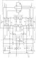
한편, 출력 트랜스미션 게이트(20)는 도 2의 출력 스위치(11)에 대응되는 것으로, 복수개의 트랜스미션 스위치(TG1, TG2, TG3, TG4)를 가진다.On the other hand, the
출력 트랜스미션 게이트(20)에 포함된 복수개의 트랜스미션 스위치(TG1, TG2, TG3, TG4)들은 복수개의 트랜스미션 제어신호(TSW1, TSW2, TSW3, TSW4) 및 이들의 상보 트랜스미션 제어신호(TSW1B, TSW2B, TSW3B, TSW4B)에 응답하여, 제1출력 버퍼(10_1)와 제2출력 버퍼(10_2)에서 증폭된 아날로그 영상 신호인 소스 라인 구동 신호를 소스 라인(Y1, Y2)으로 전송한다. 소스 라인에 연결된 부하(load)(30_1, 30_2)에 대한 구성 및 출력 보호 저항(RP1, RP2)에 대한 설명은 도 2에서 설명된 것과 동일하므로 이에 대한 구체적 설명은 생략하기로 한다.The plurality of transmission switches TG1, TG2, TG3 and TG4 included in the
예컨대, 제1출력 버퍼(10_1)에서 출력된 소스 라인 구동 신호를 전압레벨이 하이레벨(high level)이고, 제2출력 버퍼(10_2)에서 출력된 소스 라인 구동 신호 의 전압레벨이 로우레벨(low level)일 수 있다. 이에 출력 트랜스미션 게이트(20)는 소스 라인(Y1, Y2)에 모두 하이레벨을 가지는 소스 라인 구동 신호를 전송할 수도 있고, 모두 로우레벨을 가지는 소스 라인 구동 신호를 전송할 수도 있다. 또한, 소스 라인(Y1)에는 하이레벨을 가지는 소스 라인 구동 신호를 전송하고, 소스 라인(Y2)에는 로우레벨을 가지는 소스 라인 구동 신호를 전송할 수 있으며, 반대로 소스 라인(Y1)에는 로우레벨을 가지는 소스 라인 구동 신호를 전송하고, 소스 라 인(Y2)에는 하이레벨을 가지는 소스 라인 구동 신호를 전송할 수도 있다.For example, when the voltage level of the source line driving signal output from the first output buffer 10_1 is a high level and the voltage level of the source line driving signal output from the second output buffer 10_2 is low level. Accordingly, the
한편, 상기 출력 트랜스미션 게이트(20)는 복수개의 트랜스미션 스위치(TG1, TG2, TG3, TG4)를 가지는바, 복수개의 트랜스미션 스위치(TG1, TG2, TG3, TG4)가 가지는 저항성분으로 인해 슬루 레이트(SR)가 낮아져, 슬루잉 타임(slewing time)이 길어지는 문제점이 있다. 또한, 소스 드라이버(51)에 상기 출력 트랜스미션 게이트(20)가 포함되므로, 상기 소스 드라이버(51)를 가지는 디스플레이 구동장치의 레이아웃(layout) 면적이 증가한다는 문제점이 있다.The
도 4는 본 발명의 실시예에 따른 스플릿 레일-투-레일 출력버퍼를 가지는 소스 드라이버를 개략적으로 나타내는 도면이다.4 is a diagram schematically illustrating a source driver having a split rail-to-rail output buffer according to an embodiment of the present invention.
도 4의 소소 드라이버(52)에는 도 3의 소스 드라이버(51)과 달리 출력 트랜스미션 게이트가 존재하지 않는다는 것을 확인할 수 있다. 본 발명에서는 소스 드라이버(52)의 출력 트랜스미션 게이트를 제거하는 대신에, 출력 트랜스미션 게이트를 스플릿 레일-투-레일 출력버퍼(100)에 포함시켜, 높은 슬루 레이트(SR)를 구현하여 슬루잉 타임(slewing time)을 줄이고, 소스 드라이버(52)를 가지는 디스플레이 구동장치의 레이아웃(layout) 면적을 줄이고자 한다.The
본 발명의 실시예에 따른 스플릿 레일-투-레일 출력버퍼(100)는 제1출력 버퍼(100h), 제2출력 버퍼(100l) 및 피드백 회로(feedback circuit)들(160_1, 160_2, 160_3, 160_4)을 포함한다.The split rail-to-
상기 제1출력 버퍼(100h)는 제1전압 레일(VDD2)과 제2전압 레일(VDD2ML) 사이에서 구동되며, 제1제어신호(SW1)에 응답하여 제1출력단자(Vouth_1)로 소스라인 구동 신호를 출력하고, 제2제어신호(SW2)에 응답하여 제2출력단자(Voutl_1)로 소스라인 구동 신호를 출력한다.The
상기 제2출력 버퍼(100l)는 제3전압 레일(VDD2MH)과 제4전압 레일(VSS2) 사이에서 구동되며, 상기 제1제어신호(SW1)에 응답하여 제3출력단자(Vouth_2)로 소스라인 구동 신호를 출력하고, 상기 제2제어신호(SW2)에 응답하여 제4출력단자(Voutl_2)로 소스라인 구동 신호를 출력한다.The second output buffer 100l is driven between the third voltage rail VDD2MH and the fourth voltage rail VSS2 and is connected to the third output terminal Vouth_2 in response to the first control signal SW1, And outputs a source line driving signal to the fourth output terminal Voutl_2 in response to the second control signal SW2.
상기 피드백 회로(160_1, 160_2, 160_3, 160_4)들은 상기 제1제어신호(SW1)와 상기 제2제어신호(SW2)에 응답하여, 상기 출력단자들(Vouth_1, Voutl_1, Vouth_2, Voutl_2)과 상기 출력 버퍼들(100h, 100l)의 네거티브 입력단자를 연결한다.In response to the first control signal SW1 and the second control signal SW2, the feedback circuits 160_1, 160_2, 160_3, and 160_4 are connected to the output terminals Vouth_1, Voutl_1, Vouth_2, Voutl_2, And connects the negative input terminals of the
상기 제1출력 버퍼(100h)의 상기 제1출력단자(Vouth_1)와 상기 제2출력 버퍼(100l)의 상기 제3출력단자(Vouth_2)가 서로 연결되며, 상기 제1출력 버퍼(100h)의 상기 제2출력단자(Voutl_1)와 상기 제2출력 버퍼(100l)의 상기 제4출력단자(Voutl_2)가 서로 연결된다.The first output terminal (Vouth_l) of the first output buffer (100h) and the third output terminal (Vouth_2) of the second output buffer (100l) are connected to each other, The second output terminal (Voutl_1) and the fourth output terminal (Voutl_2) of the second output buffer (1001) are connected to each other.
본 발명에 따른 스플릿 레일-투-레일 출력버퍼(100)는 제1출력 버퍼(100h)와 제2출력 버퍼(100l) 각각이 두개의 출력 단자를 가지기 때문에, 총 4개의 피드백 회로가 필요하다. 결국, 상기 피드백 회로는 제1피드팩 회로(160_1), 제2피드팩 회로(160_2), 제3피드팩 회로(160_3) 및 제4피드팩 회로(160_4)를 포함한다.The split rail-to-
상기 제1제어신호(SW1) 및 제2제어신호(SW2)에 응답하여, 상기 제1출력 버퍼(100h) 및 상기 제2출력 버퍼(100l)의 출력단자로 소스 라인 구동 신호가 출력되 고, 상기 출력단자와 제1출력 버퍼(100h), 제2출력 버퍼(100l)가 피드백되는 원리를 구체적으로 살펴본다.In response to the first control signal SW1 and the second control signal SW2, a source line driving signal is outputted to the output terminals of the
상기 제1제어신호(SW1)에 응답하여(예컨대, 제1제어신호(SW1)가 하이레벨인 경우), 상기 제1출력 버퍼(100h)의 상기 제1출력단자(Vouth_1)로 소스라인 구동 신호가 출력되며, 제1피드팩 회로(160_1)는 상기 제1출력 버퍼(100h)의 상기 제1출력단자(Vouth_1)와 상기 제1출력 버퍼(100h)의 네거티브 입력단자를 연결하여, 제1출력 버퍼(100h)의 네거티브 피드백 회로를 구성한다.The source line driving signal Vout1 is supplied to the first output terminal Vouth_1 of the
상기 제1제어신호(SW1)에 응답하여(예컨대, 제1제어신호(SW1)가 로우레벨인 경우), 상기 제2출력 버퍼(100l)의 상기 제3출력단자(Vouth_2)로 소스라인 구동 신호가 출력되며, 제3피드팩 회로(160_3)는 상기 제2출력 버퍼(100l)의 상기 제3출력단자(Vouth_2)와 상기 제2출력 버퍼(100l)의 네거티브 입력단자를 연결하는 제2출력 버퍼(100l)의 네거티브 피드백 회로를 구성한다.(For example, when the first control signal SW1 is at the low level), the source line driving signal Vss_2 is supplied to the third output terminal Vouth_2 of the second output buffer 1001 in response to the first control signal SW1 And the third feed pack circuit 160_3 is connected to the second output buffer 1001 and the second output buffer 1001. The third feed pack circuit 160_3 is connected to the third output terminal Vouth_2 of the second output buffer 1001 and the negative input terminal of the second output buffer 1001, And constitute a negative feedback circuit of the transistor 100l.
상기 제2제어신호(SW2)에 응답하여(예컨대, 상기 제2제어신호(SW2)가 하이레벨인 경우), 상기 제1출력 버퍼(100h)의 상기 제2출력단자(Voutl_1)로 소스라인 구동 신호가 출력되며, 제2피드팩 회로(160_2)는 상기 제1출력 버퍼(100h)의 상기 제2출력단자(Voutl_1)와 상기 제1출력 버퍼(100h)의 네거티브 입력단자를 연결하는 제1출력 버퍼(100h)의 네거티브 피드백 회로를 구성한다.(For example, when the second control signal SW2 is at a high level) in response to the second control signal SW2, source line driving is performed to the second output terminal Voutl_1 of the
상기 제2제어신호(SW2)에 응답하여(예컨대, 상기 제2제어신호(SW2)가 로우레벨인 경우), 상기 제2출력 버퍼(100l)의 상기 제4출력단자(Voutl_2)로 소스라인 구동 신호가 출력되며, 제4피드백 회로(160_4)는 상기 제2출력 버퍼(100l)의 상기 제 4출력단자(Voutl_2)와 상기 제2출력 버퍼(100l)의 네거티브 입력단자를 연결하는 제2출력 버퍼(100l)의 네거티브 피드백 회로를 구성한다.In response to the second control signal SW2 (for example, when the second control signal SW2 is at the low level), the source
상기 제1피드백 회로(160_1)는 제1제어신호(SW1)가 하이레벨이면 제2제어신호(SW2)의 신호레벨에 관계없이 온(on)되는 스위칭 소자일 수 있으며, 상기 제2피드백 회로(160_2)는 제2제어신호(SW2)가 하이레벨이면 제1제어신호(SW1)의 신호레벨에 관계없이 온(on)되는 스위칭 소자일 수 있다.The first feedback circuit 160_1 may be a switching element that is turned on regardless of the signal level of the second control signal SW2 when the first control signal SW1 is at a high level, 160_2 may be a switching element that is turned on regardless of the signal level of the first control signal SW1 when the second control signal SW2 is at a high level.
또한, 상기 제3피드백 회로(160_3)는 제1제어신호(SW1)가 로우레벨이면 제2제어신호(SW2)의 신호레벨에 관계없이 온(on)되는 스위칭 소자일 수 있으며, 상기 제4피드백 회로(160_4)는 제2제어신호(SW2)가 로우레벨이면 제1제어신호(SW1)의 신호레벨에 관계없이 온(on)되는 스위칭 소자일 수 있다.The third feedback circuit 160_3 may be a switching element that is turned on regardless of the signal level of the second control signal SW2 when the first control signal SW1 is at a low level, The circuit 160_4 may be a switching element that is turned on regardless of the signal level of the first control signal SW1 when the second control signal SW2 is at a low level.
본 발명의 스플릿 레일 투 레일 출력버퍼(100)에 관한 것으로, 상기 제2전압 레일(VDD2ML)의 전압은 상기 제1전압 레일(VDD2)과 상기 제4전압 레일(VSS2) 사이의 전위차의 반이거나 반보다 큰 값일 수 있다. 또한, 상기 제3전압 레일(VDD2MH)의 전압은 상기 제1전압 레일(VDD2)과 상기 제4전압 레일(VSS2) 사이의 전위차의 반이거나 반보다 작은 값일 수 있다.In the split rail to rail
예컨대, 제1전압 레일(VDD2)의 전압이 10V이고 제4전압 레일(VSS2)의 전압이 0V인 경우, 제2전압 레일(VDD2ML)의 전압은 5V이거나 5V보다 조금 큰 값을 가질 수 있고, 제3전압 레일(VDD2MH)의 전압은 5V이거나 5V보다 조금 작은 값을 가질 수 있다.For example, when the voltage of the first voltage rail VDD2 is 10V and the voltage of the fourth voltage rail VSS2 is 0V, the voltage of the second voltage rail VDD2ML may be 5V or slightly larger than 5V, The voltage of the third voltage rail VDD2MH may be 5V or slightly less than 5V.
도 5는 도 4에 사용되는 스플릿 레일-투-레일 출력버퍼의 제1출력버퍼를 나 타내는 회로도이다.5 is a circuit diagram illustrating the first output buffer of the split rail-to-rail output buffer used in FIG.
도 5를 참조하면, 제1출력 버퍼(100h)는 입력 회로(110h), 전류 합 회로(120h), 바이어스 회로(125h), 스위치 회로(130h_1, 130h_2), 출력 회로(140h_1, 140h_2), 보상 커패시터부(150h) 및 쇼트방지부(170h)를 포함한다.5, the
입력 스테이지(input stage)라고도 불리는 입력 회로(110h)는 제1차동 증폭기와 제2차동 증폭기를 포함한다.An
상기 제1차동 증폭기는 제3NMOSFET(N-channel metal oxide semiconductor field effect transistor; N3h)를 통하여 제2전압 레일(VDD2ML)에 접속된 NMOSFET 쌍(N1h과 N2h)을 포함한다. NMOSFET 쌍(N1h과 N2h)은 공통 소스 구조(common source configuration)를 갖는다. 전류 원(current source)의 기능을 수행하는 제3NMOSFET(N3h)는 제1바이어스 제어 전압(VB1h)에 응답하여 상기 제1차동 증폭기로 공급되는 바이어스 전류의 양을 제어한다. NMOSFET 쌍(N1h과 N2h) 각각의 드레인은 제1전류 미러(121h)의 각 노드(N11h과 N12h)에 접속된다.The first differential amplifier includes an NMOSFET pair N1h and N2h connected to the second voltage rail VDD2ML through a third NMOSFET N3h. The NMOSFET pair (N1h and N2h) has a common source configuration. A third NMOSFET N3h, which functions as a current source, controls the amount of bias current supplied to the first differential amplifier in response to the first bias control voltage VB1h. The drains of the respective NMOSFET pairs N1h and N2h are connected to the respective nodes N11h and N12h of the first
제2차동 증폭기는 제3PMOSFET(P-channel metal oxide semiconductor field effect transistor; P3h)를 통하여 제1전압 레일(VDD2)에 접속된 PMOSFET 쌍(P1h 과 P2h)을 포함한다. PMOSFET 쌍(P1h과 P2h)은 공통 소스 구조를 갖는다. 전류 원의 기능을 수행하는 제3PMOSFET(P3h)는 제2바이어스 제어 전압(VB2h)에 응답하여 상기 제2 차동 증폭기로 공급되는 바이어스 전류의 양을 제어한다. PMOSFET 쌍(P1h과 P2h) 각각의 드레인은 제2전류 미러(123h)의 각 노드(N21h과 N22h)에 접속된다.The second differential amplifier includes a pair of PMOSFETs P1h and P2h connected to the first voltage rail VDD2 through a third P-channel metal oxide semiconductor field effect transistor (P3h). The PMOSFET pair (P1h and P2h) has a common source structure. The third PMOSFET P3h which performs the function of the current source controls the amount of the bias current supplied to the second differential amplifier in response to the second bias control voltage VB2h. The drains of the PMOSFET pair P1h and P2h are connected to the respective nodes N21h and N22h of the second
상기 제1전압 레일(VDD2)은 제1전압을 공급하고, 상기 제2전압 레일(VDD2ML) 은 제1전압 보다 낮은 제2전압을 공급한다.The first voltage rail VDD2 supplies a first voltage and the second voltage rail VDD2ML supplies a second voltage lower than the first voltage.
상기 제1차동 증폭기는 제1차동 입력 신호들(INP1와 INN1)의 전압 차이에 응답하여 제1차동 전류들을 발생한다. 상기 제2차동 증폭기는 제1차동 입력 신호들(INP1와 INN1)의 전압 차이에 응답하여 제2차동 전류들을 발생한다.The first differential amplifier generates first differential currents in response to a voltage difference between the first differential input signals INP1 and INN1. The second differential amplifier generates second differential currents in response to a voltage difference between the first differential input signals INP1 and INN1.
입력 회로(110h)는 폴디드 캐스코드(folded cascode) 연산 트랜스컨덕턴스 증폭기(Operational Transconductance Amplifier; OTA)이다. 상기 폴디드 캐스코드 OTA는 제1차동 입력 신호들(INP1와 INN1)의 전압 차이를 출력 노드(NOh)의 출력 전압 (Vouth_1, Voutl_1)을 결정하기 위한 차동 전류들로 변환한다.The
전류 합 회로(120h)는 제1전류 미러(121h)와 제2전류 미러(123h)을 포함한다. 제1전류 미러(121h)와 제2전류 미러(123l) 각각은 캐스코드 전류 미러로 구현될 수도 있다.The
제1캐스코드 전류 미러(121h)는 제1전압 레일(VDD2)과 바이어스 회로(125h) 사이에 접속된다. 제1캐스코드 전류 미러(121h)는 다수의 PMOSFET들(P4h, P5h, P6h, 및 P7h)을 포함한다. 다수의 PMOSFET들(P4h와 P6h)은 공통 게이트 증폭기를 구성한다. 제1캐스코드 전류 미러(121h)는 제1차동 전류들 또는 제3바이어스 제어 전압(VB3h) 중에서 적어도 하나에 응답하여 제1출력회로(140h_1)의 제1트랜지스터(P10h) 및 제2출력회로(140h_2)의 제3트랜지스터(P11h)에 흐르는 전류를 제어하기 위한 제1제어 전압을 제1제어 노드(PUh)로 출력한다. 제1트랜지스터(P10h) 및 제3트랜지스터(P11h)는 PMOSFET로 구현될 수 있다.The first cascode
제2캐스코드 전류 미러(123h)는 바이어스 회로(125h)와 제2전압 레 일(VDD2ML) 사이에 접속된다. 제2캐스코드 전류 미러(123h)는 다수의 NMOSFET들(N4h, N5h, N6h, 및 N7h)을 포함한다. 다수의 NMOSFET들(N4h와 N6h)은 공통 게이트 증폭기를 구성한다. 제2캐스코드 전류 미러(123h)는 제2차동 전류들 또는 제4바이어스 제어 전압(VB4h) 중에서 적어도 하나에 응답하여 제1출력회로(140h_1)의 제2트랜지스터(N10h) 및 제2출력회로(140h_2)의 제4트랜지스터(N11h)에 흐르는 전류를 제어하기 위한 제2제어 전압을 제2제어 노드(PDh)로 출력한다. 제2트랜지스터(N10h) 및 제4트랜지스터(N11h)는 NMOSFET로 구현될 수 있다.The second cascode
바이어스 회로(125h)는 플로팅 전류 원(floating current source)이라고도 불리는 제1바이어스 회로(126h)와 플로팅 클래스 AB 컨트롤(floating class AB control)이라고도 불리는 제2바이어스 회로(128h)를 포함한다.The
제1캐스코드 전류 미러(121h)와 제2캐스코드 전류 미러(123h) 사이에 접속되는 제1바이어스 회로(126h)는 제5바이어스 제어 전압(VB5h)과 제6바이어스 제어 전압 (VB6h)에 응답하여 제어된다.The
제1제어 노드(PUh)와 제2제어 노드(PDh) 사이에 접속되는 제2바이어스 회로(128h)는 제7바이어스 제어 전압(VB7h)과 제8바이어스 제어 전압(VB8h)에 응답하여 제1출력회로(140h_1)와 제2출력회로(140h_2)에 흐르는 전류, 예컨대 정적 전류(static current 또는 quiescent current)의 양을 제어한다.A
입력 회로(110h)와 전류 합 회로(120h)는 제1출력회로(140h_1)와 제2출력회로(140h_2)에 흐르는 전류의 레벨을 제어한다. 즉, 입력 회로(110h)는 제1차동 입력 신호들(INP1와 INN1)의 전압 차이에 응답하여 제1차동 전류들과 제2차동 전류들 을 발생한다. 상기 제1차동 전류들과 상기 제2차동 전류들은 전류 합 회로(120h)로 전송된다. 전류 합 회로(120h)는 제1캐스코드 전류 미러(121h)와 제2캐스코드 전류 미러(123h)를 사용하여 제1제어 노드(PUh)의 전압 레벨과 제2제어 노드(PDh)의 전압 레벨을 제어한다.The
또한, 전류 합 회로(120h)와 바이어스 회로(125h)는 제1출력버퍼(100h)의 제어 유닛을 구성한다. 상기 제어 유닛은 입력 회로(110h)에 의하여 발생한 차동 전류들, 예컨대 제1차동 전류들과 제2차동 전류들에 응답하여 제1출력회로(140h_1)와 제2출력회로(140h_2)를 통하여 흐르는 전류의 양을 제어한다.The
스위치 회로는 제1스위치 회로(130h_1)와 제2스위치 회로(130h_2)를 포함한다.The switch circuit includes a first switch circuit 130h_1 and a second switch circuit 130h_2.
제1스위치 회로(130h_1)는, 제1제어신호(SW1) 또는 상기 제1제어신호(SW1)와 상보적인 상보 제1제어신호(SW1B) 중에서 적어도 하나에 응답하여, 제1출력 회로(140h_1)의 제1트랜지스터(P10h)의 게이트를 제1제어 노드(PUh)와 제1전압 레일(VDD2) 중에서 어느 하나에 접속하고 제1출력 회로(140h_1)의 제2트랜지스터(N10h)의 게이트를 제2제어 노드(PDh)와 제2전압 레일(VDD2ML) 중에서 어느 하나에 접속한다.The first switch circuit 130h_1 is connected to the first output circuit 140h_1 in response to at least one of the first control signal SW1 or the complementary first control signal SW1B complementary to the first control signal SW1, The gate of the first transistor P10h of the first output circuit 140h_1 is connected to either the first control node PUh or the first voltage rail VDD2 and the gate of the second transistor N10h of the first output circuit 140h_1 is connected to the second And is connected to either the control node PDh or the second voltage rail VDD2ML.
제1스위치 회로(130h_1)는 다수의 스위치들(S1h 내지 S4h)을 포함한다. 제1스위치(S1h)는 제1제어신호(SW1)와 상보 제1제어신호(SW1B)에 응답하여 제1제어 노드(PUh)와 제1트랜지스터(P10h)의 게이트의 접속을 제어한다. 제2스위치(S2h)는 제1제어신호(SW1)와 상보 제1제어신호(SW1B)에 응답하여 제2제어 노드(PDh)와 제2트 랜지스터(N10h)의 게이트의 접속을 제어한다. 제3스위치(S3h)는 제1제어신호(SW1)에 응답하여 제1전압 레일(VDD2)과 제1트랜지스터(P10h)의 게이트의 접속을 제어하고, 제4스위치(S4h)는 상보 제1제어신호(SW1B)에 응답하여 제2전압 레일(VDD2ML)과 제2트랜지스터(N10h)의 게이트의 접속을 제어한다.The first switch circuit 130h_1 includes a plurality of switches S1h to S4h. The first switch S1h controls the connection between the first control node PUh and the gate of the first transistor P10h in response to the first control signal SW1 and the complementary first control signal SW1B. The second switch S2h controls the connection of the gates of the second control node PDh and the second transistor N10h in response to the first control signal SW1 and the complementary first control signal SW1B. The third switch S3h controls the connection of the gates of the first transistor P10h and the first voltage rail VDD2 in response to the first control signal SW1 and the fourth switch S4h controls the connection of the gates of the first transistor P10h, And controls the connection of the gates of the second voltage rail VDD2ML and the second transistor N10h in response to the signal SW1B.
본 발명의 실시예에서 제1스위치(S1h)와 제2스위치(S2h) 각각은 트랜스미션 게이트(transmission gate)로 구현되고, 제3스위치(S3h)는 PMOSFET로 구현되고, 제4스위치(S4h)는 NMOSFET로 구현될 수 있다. 그러나, 제1스위치(S1h)와 제2스위치(S2h) 각각이 NMOSFET 또는 PMOSFET로 구현될 수도 있다.In the embodiment of the present invention, each of the first switch S1h and the second switch S2h is implemented as a transmission gate, the third switch S3h is implemented as a PMOSFET, and the fourth switch S4h is implemented as a PMOSFET May be implemented as an NMOSFET. However, each of the first switch S1h and the second switch S2h may be implemented as an NMOSFET or a PMOSFET.
제2스위치 회로(130h_2)는, 제2제어신호(SW2) 또는 상기 제2제어신호(SW2)와 상보적인 상보 제2제어신호(SW2B) 중에서 적어도 하나에 응답하여, 제2출력 회로(140h_2)의 제3트랜지스터(P11h)의 게이트를 제1제어 노드(PUh)와 제1전압 레일(VDD2) 중에서 어느 하나에 접속하고 제2출력 회로(140h_2)의 제4트랜지스터(N11h)의 게이트를 제2제어 노드(PDh)와 제2전압 레일(VDD2ML) 중에서 어느 하나에 접속한다.The second switch circuit 130h_2 is connected to the second output circuit 140h_2 in response to at least one of the second control signal SW2 or the complementary second control signal SW2B complementary to the second control signal SW2, The gate of the third transistor P11h of the second output circuit 140h_2 is connected to either the first control node PUh or the first voltage rail VDD2 and the gate of the fourth transistor N11h of the second output circuit 140h_2 is connected to the second And is connected to either the control node PDh or the second voltage rail VDD2ML.
제2스위치 회로(130h_2)는 다수의 스위치들(S5h 내지 S8h)을 포함한다. 제5스위치(S5h)는 제2제어신호(SW2)와 상보 제2제어신호(SW2B)에 응답하여 제1제어 노드(PUh)와 제3트랜지스터(P11h)의 게이트의 접속을 제어한다. 제6스위치(S6h)는 제2제어신호(SW2)와 상보 제2제어신호(SW2B)에 응답하여 제2제어 노드(PDh)와 제4트랜지스터(N11h)의 게이트의 접속을 제어한다. 제7스위치(S7h)는 제2제어신호(SW2)에 응답하여 제1전압 레일(VDD2)과 제3트랜지스터(P11h)의 게이트의 접속을 제어하 고, 제8스위치(S8h)는 상보 제2제어신호(SW2B)에 응답하여 제2전압 레일(VDD2ML)과 제4트랜지스터(N11h)의 게이트의 접속을 제어한다.The second switch circuit 130h_2 includes a plurality of switches S5h to S8h. The fifth switch S5h controls the connection between the gates of the first control node PUh and the third transistor P11h in response to the second control signal SW2 and the complementary second control signal SW2B. The sixth switch S6h controls the connection between the gates of the second control node PDh and the fourth transistor N11h in response to the second control signal SW2 and the complementary second control signal SW2B. The seventh switch S7h controls the connection of the gates of the first voltage rail VDD2 and the third transistor P11h in response to the second control signal SW2 and the eighth switch S8h controls the connection of the complementary second And controls the connection of the gates of the second voltage rail VDD2ML and the fourth transistor N11h in response to the control signal SW2B.
본 발명의 실시예에서 제5스위치(S5h)와 제6스위치(S6h) 각각은 트랜스미션 게이트(transmission gate)로 구현되고, 제7스위치(S7h)는 PMOSFET로 구현되고, 제8스위치(S8h)는 NMOSFET로 구현될 수 있다. 그러나, 제5스위치(S5h)와 제6스위치(S6h) 각각이 NMOSFET 또는 PMOSFET로 구현될 수도 있다.In the embodiment of the present invention, each of the fifth switch S5h and the sixth switch S6h is implemented as a transmission gate, the seventh switch S7h is implemented as a PMOSFET, the eighth switch S8h is implemented as a PMOSFET, May be implemented as an NMOSFET. However, each of the fifth switch S5h and the sixth switch S6h may be implemented as an NMOSFET or a PMOSFET.
제1제어신호(SW1)에 응답하여, 제1출력버퍼(100h)가 구동되는 구체적 원리는 다음과 같다. 예컨대, 제1레벨(예컨대, 하이 레벨(H))을 갖는 제1제어신호(SW1)와 제2레벨(예컨대, 로우 레벨(L))을 갖는 상보 제1제어신호(SW1B)에 응답하여, 제1스위치(S1h)는 제1트랜지스터(P10h)의 게이트와 제1제어 노드(PUh)를 접속하고, 제2스위치(S2h)는 제2트랜지스터(N10h)의 게이트와 제2제어 노드(PDh)를 접속하고, 제3스위치(S3h)는 제1전압 레일(VDD2)과 제1트랜지스터(P10h)의 게이트를 분리하고, 제4스위치(S4h)는 제2전압 레일(VDD2ML)과 제2트랜지스터(N10h)의 게이트를 분리한다.The specific principle by which the
그러나, 예컨대 제2레벨(예컨대, 로우 레벨(L))을 갖는 제1제어신호(SW1)와 제1레벨(예컨대, 하이 레벨(H))을 갖는 상보 제1제어신호(SW1B)에 응답하여, 제1스위치(S1h)는 제1트랜지스터(P10h)의 게이트와 제1제어 노드(PUh)를 분리하고, 제2스위치(S2h)는 제2트랜지스터(N10h)의 게이트와 제2제어 노드(PDh)를 분리하고, 제3스위치(S3h)는 제1전압 레일(VDD2)과 제1트랜지스터(P10h)의 게이트를 접속하고, 제4스위치(S4h)는 제2전압 레일(VDD2ML)과 제2트랜지스터(N10h)의 게이트를 접속한 다.However, in response to the first control signal SW1 having a second level (e.g., a low level L) and the complementary first control signal SW1B having a first level (e.g., a high level H) , The first switch S1h disconnects the gate of the first transistor P10h from the first control node PUh and the second switch S2h disconnects the gate of the second transistor N10h and the gate of the second control node PDh The third switch S3h connects the first voltage rail VDD2 and the gate of the first transistor P10h and the fourth switch S4h connects the second voltage rail VDD2ML and the second transistor P10h, And the gate of the transistor N10h is connected.
제2제어신호(SW2)에 응답하여, 제1출력버퍼(100h)가 구동되는 구체적 원리는 다음과 같다. 예컨대, 제1레벨(예컨대, 하이 레벨(H))을 갖는 제2제어신호(SW2)와 제2레벨(예컨대, 로우 레벨(L))을 갖는 상보 제2제어신호(SW2B)에 응답하여, 제5스위치(S5h)는 제3트랜지스터(P11h)의 게이트와 제1제어 노드(PUh)를 접속하고, 제6스위치(S6h)는 제4트랜지스터(N11h)의 게이트와 제2제어 노드(PDh)를 접속하고, 제7스위치(S7h)는 제1전압 레일(VDD2)과 제3트랜지스터(P11h)의 게이트를 분리하고, 제8스위치(S8h)는 제2전압 레일(VDD2ML)과 제4트랜지스터(N11h)의 게이트를 분리한다.The specific principle by which the
그러나, 예컨대 제2레벨(예컨대, 로우 레벨(L))을 갖는 제2제어신호(SW2)와 제1레벨(예컨대, 하이 레벨(H))을 갖는 상보 제2제어신호(SW2B)에 응답하여, 제5스위치(S5h)는 제3트랜지스터(P11h)의 게이트와 제1제어 노드(PUh)를 분리하고, 제6스위치(S6h)는 제4트랜지스터(N11h)의 게이트와 제2제어 노드(PDh)를 분리하고, 제7스위치(S7h)는 제1전압 레일(VDD2)과 제3트랜지스터(P11h)의 게이트를 접속하고, 제8스위치(S8h)는 제2전압 레일(VDD2ML)과 제4트랜지스터(N11h)의 게이트를 접속한다.However, in response to the second control signal SW2 having a second level (e.g., a low level L) and the complementary second control signal SW2B having a first level (e.g., a high level H) The fifth switch S5h disconnects the gate of the third transistor P11h from the first control node PUh and the sixth switch S6h disconnects the gate of the fourth transistor N11h and the gate of the second control node PDh The seventh switch S7h connects the first voltage rail VDD2 to the gates of the third transistor P11h and the eighth switch S8h is connected to the second voltage rail VDD2ML and the fourth transistor S11h. (N11h).
보상 커패시터부(150h)는 제1보상 커패시터(C1h)와 제2보상 커패시터(C2h)를 포함한다.The
제1보상 커패시터(C1h)는 출력 노드(N0h)와 제1캐스코드 전류 미러(121h)의 오른쪽 노드(N12h) 사이에 접속되고, 제2보상 커패시터(C2h)는 출력 노드(N0h)와 제2캐스코드 전류 미러(123h)의 오른쪽 노드(N22h) 사이에 접속된다. 그러나, 본 발명의 실시예에 따른 제1출력버퍼(100h)는 제1보상 커패시터(C1h)와 제2보상 커패시터(C2h) 없이도 구현될 수 있다.The first compensation capacitor C1h is connected between the output node N0h and the right node N12h of the first cascode
공통 소스 구조를 갖는 제1트랜지스터(P10h)와 제2트랜지스터(N10h)를 포함하는 제1출력회로(140h_1)는 제1전압 레일(VDD2)과 제2전압 레일(VDD2ML) 사이에 접속된다. 마찬가지로, 공통 소스 구조를 갖는 제3트랜지스터(P11h)와 제4트랜지스터(N11h)를 포함하는 제2출력회로(140h_2)는 제1전압 레일(VDD2)과 제2전압 레일(VDD2ML) 사이에 접속된다.The first output circuit 140h_1 including the first transistor P10h and the second transistor N10h having the common source structure is connected between the first voltage rail VDD2 and the second voltage rail VDD2ML. Similarly, the second output circuit 140h_2 including the third transistor P11h having the common source structure and the fourth transistor N11h is connected between the first voltage rail VDD2 and the second voltage rail VDD2ML .
제1트랜지스터(P10h), 제3트랜지스터(P11h)의 바이어스 전류는 제1트랜지스터(P10h), 제3트랜지스터(P11h)의 게이트로 공급되는 제1제어 전압(즉, 제1제어 노드(PUh)의 전압)에 의하여 결정되고, 제2트랜지스터(N10h), 제4트랜지스터(N11h)의 바이어스 전류는 제2트랜지스터(N10h), 제4트랜지스터(N11h)의 게이트로 공급되는 제2제어 전압(즉, 제2제어 노드(PUh)의 전압)에 의하여 결정된다.The bias currents of the first transistor P10h and the third transistor P11h are controlled by the first control voltage PUh supplied to the gates of the first transistor P10h and the third transistor P11h And the bias currents of the second transistor N10h and the fourth transistor N11h are determined by the second control voltage supplied to the gates of the second transistor N10h and the
쇼트방지부(170h)는 제1쇼트방지 스위치(S9h) 및 제2쇼트방지 스위치(S10h)를 포함한다.The
제1쇼트방지 스위치(S9h)는 출력 노드(N0h)와 상기 제1출력회로(140h_1)의 제1출력단자(Vouth_1) 사이에 접속되어, 제1제어신호(SW1)와 상보 제1제어신호(SW1B)에 응답하여 상기 출력 노드(N0h)와 상기 제1출력단자(Vouth_1)를 접속하거나 차단한다.The first short-circuiting prevention switch S9h is connected between the output node N0h and the first output terminal Vouth_1 of the first output circuit 140h_1 and outputs a first control signal SW1 and a complementary first control signal SW1 And connects or disconnects the output node (N0h) and the first output terminal (Vouth_1) in response to the first output terminal (SW1B).
제2쇼트방지 스위치(S10h)는 출력 노드(N0h)와 상기 제2출력회로(140h_2)의 제2출력단자(Voutl_1) 사이에 접속되어, 제2제어신호(SW2)와 상보 제2제어신호(SW2B)에 응답하여 상기 출력 노드(N0h)와 상기 제2출력단자(Voutl_1)를 접속하거나 차단한다.The second short-circuit prevention switch S10h is connected between the output node N0h and the second output terminal Voutl_1 of the second output circuit 140h_2 and outputs the second control signal SW2 and the complementary second control signal SW2 SW2B to connect or disconnect the output node N0h and the second output terminal Voutl_1.
도 4를 다시 참조하면, 제1출력 버퍼(100h)의 제1출력단자(Vouth_1)와 제2출력 버퍼(100l)의 제3출력단자(Vouth_2)가 서로 연결되며, 제1출력 버퍼(100h)의 제2출력단자(Voutl_1)와 제2출력 버퍼(100l)의 제4출력단자(Voutl_2)가 서로 연결된다.4, the first output terminal Vouth_1 of the
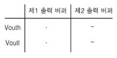
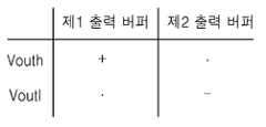
결국, 제2출력버퍼(100l)의 제3출력단자(Vouth_2)로 소스 라인 구동 신호가 출력될 때, 제1출력버퍼(100h)의 제1출력단자(Vouth_1)와 제2출력버퍼(100l)의 제3출력단자(Vouth_2) 사이의 쇼트(short)를 방지하기 위하여, 제1쇼트방지 스위치(S9h)는 상기 출력 노드(N0h)와 상기 제1출력단자(Vouth_1)의 접속을 차단한다.When the source line driving signal is output to the third output terminal Vouth_2 of the second output buffer 1001, the first output terminal Vouth_1 of the
마찬가지로, 제2출력버퍼(100l)의 제4출력단자(Voutl_2)로 소스 라인 구동 신호가 출력될 때, 제1출력버퍼(100h)의 제2출력단자(Voutl_1)와 제2출력버퍼(100l)의 제4출력단자(Voutl_2) 사이의 쇼트(short)를 방지하기 위하여, 제2쇼트방지 스위치(S10h)는 상기 출력 노드(N0h)와 상기 제2출력단자(Voutl_1)의 접속을 차단한다.Likewise, when the source line driving signal is outputted to the fourth output terminal Voutl_2 of the second output buffer 1001, the second output terminal Voutl_1 of the
도 6은 도 4에 사용되는 스플릿 레일-투-레일 출력버퍼의 제2출력버퍼를 나타내는 회로도이다.6 is a circuit diagram showing a second output buffer of the split rail-to-rail output buffer used in FIG.
도 6을 참조하면, 제2출력 버퍼(100l)는 입력 회로(110l), 전류 합 회 로(120l), 바이어스 회로(125l), 스위치 회로(130l_1, 130l_2), 출력 회로(140l_1, 140l_2), 보상 커패시터부(150l) 및 쇼트방지부(170l)를 포함한다.6, the second output buffer 100l includes an
입력 스테이지라고도 불리는 입력 회로(110l)는 제3차동 증폭기와 제4차동 증폭기를 포함한다.An
상기 제3차동 증폭기는 제3NMOSFET(N3l)를 통하여 제4전압 레일(VSS2)에 접속된 NMOSFET 쌍(N1l과 N2l)을 포함한다. NMOSFET 쌍(N1l과 N2l)은 공통 소스 구조를 갖는다. 전류 원의 기능을 수행하는 제3NMOSFET(N3l)는 제1바이어스 제어 전압(VB1l)에 응답하여 상기 제3차동 증폭기로 공급되는 바이어스 전류의 양을 제어한다. NMOSFET 쌍(N1l과 N2l) 각각의 드레인은 제3전류 미러(121l)의 각 노드(N11l과 N12l)에 접속된다.The third differential amplifier includes an NMOSFET pair N1l and N2l connected to a fourth voltage rail VSS2 through a third NMOSFET N3l. The NMOSFET pair (Nl and Nl) has a common source structure. The third NMOSFET N31 performing the function of the current source controls the amount of the bias current supplied to the third differential amplifier in response to the first bias control voltage VB1l. The drains of the NMOSFET pair N1l and N2l are connected to the respective nodes N111 and N121 of the third current mirror 121l.
제4차동 증폭기는 제3PMOSFET(P3l)를 통하여 제3전압 레일(VDD2MH)에 접속된 PMOSFET 쌍(P1l 과 P2l)을 포함한다. PMOSFET 쌍(P1l과 P2l)은 공통 소스 구조를 갖는다. 전류 원의 기능을 수행하는 제3PMOSFET(P3l)는 제2바이어스 제어 전압(VB2l)에 응답하여 상기 제4차동 증폭기로 공급되는 바이어스 전류의 양을 제어한다. PMOSFET 쌍(P1l과 P2l) 각각의 드레인은 제4전류 미러(123l)의 각 노드 (N21l과 N22l)에 접속된다.The fourth differential amplifier includes a pair of PMOSFETs P1l and P2l connected to the third voltage rail VDD2MH through a third PMOSFET P3l. The PMOSFET pair (P1l and P2l) has a common source structure. The third PMOSFET P3l that performs the function of the current source controls the amount of the bias current supplied to the fourth differential amplifier in response to the second bias control voltage VB2l. The drains of the PMOSFET pairs P1l and P2l are connected to the respective nodes N21l and N22l of the fourth current mirror 123l.
상기 제3전압 레일(VDD2MH)은 제3전압을 공급하고, 상기 제4전압 레일(VSS2)은 제3전압 보다 낮은 제4전압을 공급한다.The third voltage rail VDD2MH supplies a third voltage and the fourth voltage rail VSS2 supplies a fourth voltage lower than the third voltage.
상기 제3차동 증폭기는 제2차동 입력 신호들(INP2와 INN2)의 전압 차이에 응답하여 제3차동 전류들을 발생한다. 상기 제4차동 증폭기는 제2차동 입력 신호 들(INP2와 INN2)의 전압 차이에 응답하여 제4차동 전류들을 발생한다.The third differential amplifier generates third differential currents in response to a voltage difference between the second differential input signals INP2 and INN2. The fourth differential amplifier generates fourth differential currents in response to a voltage difference between the second differential input signals INP2 and INN2.
입력 회로(110l)는 폴디드 캐스코드 연산 트랜스컨덕턴스 증폭기(Operational Transconductance Amplifier; OTA)이다. 상기 폴디드 캐스코드 OTA는 제2차동 입력 신호들(INP2와 INN2)의 전압 차이를 출력 노드(NOl)의 출력 전압(Vouth_2, Voutl_2)을 결정하기 위한 차동 전류들로 변환한다.The
전류 합 회로(120l)는 제3전류 미러(121l)와 제4전류 미러(123l)를 포함한다. 제3전류 미러(121l)와 제4전류 미러(123l) 각각은 캐스코드 전류 미러로 구현될 수도 있다.The current sum circuit 120l includes a third current mirror 121l and a fourth current mirror 123l. Each of the third current mirror 121l and the fourth current mirror 123l may be implemented as a cascode current mirror.
제3캐스코드 전류 미러(121l)는 제3전압 레일(VDD2MH)과 바이어스 회로(125l) 사이에 접속된다. 제3캐스코드 전류 미러(121l)는 다수의 PMOSFET들(P4l, P5l, P6l, 및 P7l)을 포함한다. 다수의 PMOSFET들(P4l와 P6l)은 공통 게이트 증폭기를 구성한다. 제3캐스코드 전류 미러(121l)는 제3차동 전류들 또는 제3바이어스 제어 전압(VB3l) 중에서 적어도 하나에 응답하여 제3출력회로(140l_1)의 제5트랜지스터(P10l) 및 제4출력회로(140l_2)의 제7트랜지스터(P11l)에 흐르는 전류를 제어하기 위한 제3제어 전압을 제3제어 노드(PUl)로 출력한다. 제5트랜지스터(P10l) 및 제7트랜지스터(P11l)는 PMOSFET로 구현될 수 있다.The third cascode current mirror 121l is connected between the third voltage rail VDD2MH and the bias circuit 125l. The third cascode current mirror 121l includes a plurality of PMOSFETs P4l, P5l, P6l, and P7l. The plurality of PMOSFETs P4l and P6l constitute a common gate amplifier. The third cascode current mirror 121l is responsive to at least one of the third differential currents or the third bias control voltage VB3l to turn on the fifth transistor P10l and the fourth output circuit To the third control node PU1, a third control voltage for controlling the current flowing in the seventh transistor P111 of the first transistor P111. The fifth transistor P10l and the seventh transistor P11l may be implemented as PMOSFETs.
제4캐스코드 전류 미러(123l)는 바이어스 회로(125l)와 제4전압 레일(VSS2) 사이에 접속된다. 제4캐스코드 전류 미러(123l)는 다수의 NMOSFET들(N4l, N5l, N6l, 및 N7l)을 포함한다. 다수의 NMOSFET들(N4l와 N6l)은 공통 게이트 증폭기를 구성한다. 제4캐스코드 전류 미러(123l)는 제4차동 전류들 또는 제4바이어스 제어 전압(VB4l) 중에서 적어도 하나에 응답하여 제3출력회로(140l_1)의 제6트랜지스터(N10l) 및 제4출력회로(140l_2)의 제8트랜지스터(N11l)에 흐르는 전류를 제어하기 위한 제4제어 전압을 제4제어 노드(PDl)로 출력한다. 제6트랜지스터(N10l) 및 제8트랜지스터(N11l)는 NMOSFET로 구현될 수 있다.The fourth cascode current mirror 123l is connected between the
바이어스 회로(125l)는 플로팅 전류 원이라고도 불리는 제3바이어스 회로(126l)와 플로팅 클래스 AB 컨트롤이라고도 불리는 제4바이어스 회로(128l)를 포함한다.The
제3캐스코드 전류 미러(121l)와 제4캐스코드 전류 미러(123l) 사이에 접속되는 제3바이어스 회로(126l)는 제5바이어스 제어 전압(VB5l)과 제6바이어스 제어 전압 (VB6l)에 응답하여 제어된다.The
제3제어 노드(PUl)와 제4제어 노드(PDl) 사이에 접속되는 제4바이어스 회로(128l)는 제7바이어스 제어 전압(VB7l)과 제8바이어스 제어 전압(VB8l)에 응답하여 제3출력회로(140l_1)와 제4출력회로(140l_2)에 흐르는 전류, 예컨대 정적 전류의 양을 제어한다.The fourth bias circuit 128l connected between the third control node PU1 and the fourth control node PD1 is connected to the third output node N1 in response to the seventh bias control voltage VB7l and the eighth bias control voltage VB8l, For example, the amount of static current flowing in the circuit 140l_1 and the fourth output circuit 140l_2.
입력 회로(110l)와 전류 합 회로(120l)는 제3출력회로(140l_1)와 제4출력회로(140l_2)에 흐르는 전류의 레벨을 제어한다. 즉, 입력 회로(110l)는 제2차동 입력 신호들(INP2와 INN2)의 전압 차이에 응답하여 제3차동 전류들과 제4차동 전류들을 발생한다. 상기 제3차동 전류들과 상기 제4차동 전류들은 전류 합 회로(120l)로 전송된다. 전류 합 회로(120l)는 제3캐스코드 전류 미러(121l)와 제4캐스코드 전류 미러(123l)를 사용하여 제3제어 노드(PUl)의 전압 레벨과 제4제어 노드(PDl)의 전 압 레벨을 제어한다.The
또한, 전류 합 회로(120l)와 바이어스 회로(125l)는 제2출력버퍼(100l)의 제어 유닛을 구성한다. 상기 제어 유닛은 입력 회로(110l)에 의하여 발생한 차동 전류들, 예컨대 제3차동 전류들과 제4차동 전류들에 응답하여 제3출력회로(140l_1)와 제4출력회로(140l_2)를 통하여 흐르는 전류의 양을 제어한다.Further, the
스위치 회로는 제3스위치 회로(130l_1)와 제4스위치 회로(130l_2)를 포함한다.The switch circuit includes a third switch circuit 130l_1 and a fourth switch circuit 130l_2.
제3스위치 회로(130l_1)는, 제1제어신호(SW1) 또는 상기 제1제어신호(SW1)와 상보적인 상보 제1제어신호(SW1B) 중에서 적어도 하나에 응답하여, 제3출력 회로(140l_1)의 제5트랜지스터(P10l)의 게이트를 제3제어 노드(PUl)와 제3전압 레일(VDD2MH) 중에서 어느 하나에 접속하고 제4출력 회로(140l_1)의 제6트랜지스터(N10l)의 게이트를 제4제어 노드(PDl)와 제4전압 레일(VSS2) 중에서 어느 하나에 접속한다.The third switch circuit 130l_1 is connected to the third output circuit 140l_1 in response to at least one of the first control signal SW1 or the complementary first control signal SW1B complementary to the first control signal SW1, The gate of the fifth transistor P101 of the fourth output circuit 1401_1 is connected to either the third control node PU1 or the third voltage rail VDD2MH and the gate of the sixth transistor N101 of the fourth output circuit 1401_1 is connected to the fourth And is connected to either the control node PD1 or the fourth voltage rail VSS2.
제3스위치 회로(130l_1)는 다수의 스위치들(S1l 내지 S4l)을 포함한다. 제11스위치(S1l)는 제1제어신호(SW1)와 상보 제1제어신호(SW1B)에 응답하여 제3제어 노드(PUl)와 제5트랜지스터(P10l)의 게이트의 접속을 제어한다. 제12스위치(S2l)는 제1제어신호(SW1)와 상보 제1제어신호(SW1B)에 응답하여 제4제어 노드(PDl)와 제6트랜지스터(N10l)의 게이트의 접속을 제어한다. 제13스위치(S3l)는 상보 제1제어신호(SW1B)에 응답하여 제3전압 레일(VDD2MH)과 제5트랜지스터(P10l)의 게이트의 접속을 제어하고, 제14스위치(S4l)는 제1제어신호(SW1)에 응답하여 제4전압 레 일(VSS2)과 제6트랜지스터(N10l)의 게이트의 접속을 제어한다.The third switch circuit 130l_1 includes a plurality of switches S1l to S4l. The eleventh switch S1l controls the connection of the gates of the third control node PU1 and the fifth transistor P101 in response to the first control signal SW1 and the complementary first control signal SW1B. The twelfth switch S2l controls connection of the gates of the fourth control node PD1 and the sixth transistor N101 in response to the first control signal SW1 and the complementary first control signal SW1B. The thirteenth switch S3l controls the connection of the gates of the third voltage rail VDD2MH and the fifth transistor P101 in response to the complementary first control signal SW1B, And controls the connection of the gates of the sixth transistor N101 and the fourth voltage rail VSS2 in response to the signal SW1.
본 발명의 실시예에서 제11스위치(S1l)와 제12스위치(S2l) 각각은 트랜스미션 게이트(transmission gate)로 구현되고, 제13스위치(S3l)는 PMOSFET로 구현되고, 제14스위치(S4l)는 NMOSFET로 구현될 수 있다. 그러나, 제11스위치(S1l)와 제12스위치(S2l) 각각이 NMOSFET 또는 PMOSFET로 구현될 수도 있다.In the embodiment of the present invention, each of the eleventh switch S1l and the twelfth switch S2l is implemented as a transmission gate, the thirteenth switch S3l is implemented as a PMOSFET, and the fourteenth switch Sl, May be implemented as an NMOSFET. However, each of the eleventh switch Sl and twelfth switch S2l may be implemented as an NMOSFET or a PMOSFET.
제4스위치 회로(130l_2)는, 제2제어신호(SW2) 또는 상기 제2제어신호(SW2)와 상보적인 상보 제2제어신호(SW2B) 중에서 적어도 하나에 응답하여, 제4출력 회로(140l_2)의 제7트랜지스터(P11l)의 게이트를 제3제어 노드(PUl)와 제3전압 레일(VDD2MH) 중에서 어느 하나에 접속하고 제4출력 회로(140l_2)의 제8트랜지스터(N11l)의 게이트를 제4제어 노드(PDl)와 제4전압 레일(VSS2) 중에서 어느 하나에 접속한다.The fourth switch circuit 1301_2 is connected to the fourth output circuit 1401_2 in response to at least one of the second control signal SW2 or the complementary second control signal SW2B complementary to the second control signal SW2, The gate of the seventh transistor P111 of the fourth output circuit 1401_2 is connected to either the third control node PU1 or the third voltage rail VDD2MH and the gate of the eighth transistor N111 of the fourth output circuit 1401_2 is connected to the fourth And is connected to either the control node PD1 or the fourth voltage rail VSS2.
제4스위치 회로(130l_2)는 다수의 스위치들(S5l 내지 S8l)을 포함한다. 제15스위치(S5l)는 제2제어신호(SW2)와 상보 제2제어신호(SW2B)에 응답하여 제3제어 노드(PUl)와 제7트랜지스터(P11l)의 게이트의 접속을 제어한다. 제16스위치(S6l)는 제2제어신호(SW2)와 상보 제2제어신호(SW2B)에 응답하여 제4제어 노드(PDl)와 제8트랜지스터(N11l)의 게이트의 접속을 제어한다. 제17스위치(S7l)는 상보 제2제어신호(SW2B)에 응답하여 제3전압 레일(VDD2MH)과 제7트랜지스터(P11l)의 게이트의 접속을 제어하고, 제18스위치(S8l)는 제2제어신호(SW2)에 응답하여 제4전압 레일(VSS2)과 제8트랜지스터(N11l)의 게이트의 접속을 제어한다.The fourth switch circuit 1301_2 includes a plurality of switches S51 to S81. The fifteenth switch S5l controls the connection between the gates of the third control node PU1 and the seventh transistor P111 in response to the second control signal SW2 and the complementary second control signal SW2B. The sixteenth switch S6l controls the connection of the gates of the fourth control node PD1 and the eighth transistor N111 in response to the second control signal SW2 and the complementary second control signal SW2B. The seventeenth switch S7l controls the connection of the gates of the seventh transistor P111 and the third voltage rail VDD2MH in response to the complementary second control signal SW2B, And controls the connection of the gates of the eighth transistor N111 and the fourth voltage rail VSS2 in response to the signal SW2.
본 발명의 실시예에서 제15스위치(S5l)와 제16스위치(S6l) 각각은 트랜스미 션 게이트(transmission gate)로 구현되고, 제17스위치(S7l)는 PMOSFET로 구현되고, 제18스위치(S8l)는 NMOSFET로 구현될 수 있다. 그러나, 제15스위치(S5l)와 제16스위치(S6l) 각각이 NMOSFET 또는 PMOSFET로 구현될 수도 있다.In the embodiment of the present invention, each of the fifteenth switch S5l and the sixteenth switch S6l is implemented as a transmission gate, the seventeenth switch S7l is implemented as a PMOSFET, the eighteenth switch S8l ) May be implemented as an NMOSFET. However, each of the fifteenth switch S5l and the sixteenth switch S6l may be implemented as an NMOSFET or a PMOSFET.
제1제어신호(SW1)에 응답하여, 제2출력버퍼(100l)가 구동되는 구체적 원리는 다음과 같다. 예컨대, 제1레벨(예컨대, 하이 레벨(L))을 갖는 제1제어신호(SW1)와 제2레벨(예컨대, 로우 레벨(L))을 갖는 상보 제1제어신호(SW1B)에 응답하여, 제11스위치(S1l)는 제5트랜지스터(P10l)의 게이트와 제3제어 노드(PUl)를 분리하고, 제12스위치(S2l)는 제6트랜지스터(N10l)의 게이트와 제4제어 노드(PDl)를 분리하고, 제13스위치(S3l)는 제3전압 레일(VDD2MH)과 제5트랜지스터(P10l)의 게이트를 접속하고, 제14스위치(S4l)는 제4전압 레일(VSS2)과 제6트랜지스터(N10l)의 게이트를 접속한다.The specific principle by which the second output buffer 1001 is driven in response to the first control signal SW1 is as follows. For example, in response to the complementary first control signal SW1B having the first level (e.g., high level L) and the second level (e.g., low level L) The eleventh switch Sl separates the gate of the fifth transistor P10l from the third control node PUl and the twelfth switch S2l disconnects the gate of the sixth transistor N10l and the fourth control node PDl, The thirteenth switch S3l connects the third voltage rail VDD2MH and the gate of the fifth transistor P101 and the fourteenth switch S4l connects the fourth voltage rail VSS2 and the sixth transistor P101, N101.
그러나, 예컨대 제2레벨(예컨대, 로우 레벨(L))을 갖는 제1제어신호(SW1)와 제1레벨(예컨대, 하이 레벨(L))을 갖는 상보 제1제어신호(SW1B)에 응답하여, 제11스위치(S1l)는 제5트랜지스터(P10l)의 게이트와 제3제어 노드(PUl)를 접속하고, 제12스위치(S2l)는 제6트랜지스터(N10l)의 게이트와 제4제어 노드(PDl)를 접속하고, 제13스위치(S3l)는 제3전압 레일(VDD2MH)과 제5트랜지스터(P10l)의 게이트를 분리하고, 제14스위치(S4l)는 제4전압 레일(VSS2)과 제6트랜지스터(N10l)의 게이트를 분리한다.However, in response to the first control signal SW1 having the second level (e.g., the low level L) and the complementary first control signal SW1B having the first level (e.g., the high level L) , The eleventh switch S1l connects the gate of the fifth transistor P10l to the third control node PUl and the twelfth switch S2l connects the gate of the sixth transistor N10l to the fourth control node PDl The thirteenth switch S3l disconnects the gates of the third voltage rail VDD2MH and the fifth transistor P101 and the fourteenth switch S4l connects the fourth voltage rail VSS2 and the sixth transistor P101, The gate of the transistor N101 is disconnected.
제2제어신호(SW2)에 응답하여, 제2출력버퍼(100l)가 구동되는 구체적 원리는 다음과 같다. 예컨대, 제1레벨(예컨대, 하이 레벨(L))을 갖는 제2제어신호(SW2)와 제2레벨(예컨대, 로우 레벨(L))을 갖는 상보 제2제어신호(SW2B)에 응답하여, 제15스위치(S5l)는 제7트랜지스터(P11l)의 게이트와 제3제어 노드(PUl)를 분리하고, 제16스위치(S6l)는 제8트랜지스터(N11l)의 게이트와 제4제어 노드(PDl)를 분리하고, 제17스위치(S7l)는 제3전압 레일(VDD2MH)과 제7트랜지스터(P11l)의 게이트를 접속하고, 제18스위치(S8l)는 제4전압 레일(VSS2)과 제8트랜지스터(N11l)의 게이트를 접속한다.The specific principle by which the second output buffer 1001 is driven in response to the second control signal SW2 is as follows. For example, in response to the second control signal SW2 having the first level (e.g., the high level L) and the complementary second control signal SW2B having the second level (e.g., the low level L) The fifteenth switch S5l disconnects the gate of the seventh transistor P11l from the third control node PUl and the sixteenth switch S6l disconnects the gate of the eighth transistor N11l and the fourth control node PDl, The seventeenth switch S7l connects the gates of the seventh transistor P111 and the third voltage rail VDD2MH and the eighteenth switch S81 connects the fourth voltage rail VSS2 and the eighth transistor N111.
그러나, 예컨대 제2레벨(예컨대, 로우 레벨(L))을 갖는 제2제어신호(SW2)와 제1레벨(예컨대, 하이 레벨(L))을 갖는 상보 제2제어신호(SW2B)에 응답하여, 제15스위치(S5l)는 제7트랜지스터(P11l)의 게이트와 제3제어 노드(PUl)를 접속하고, 제16스위치(S6l)는 제8트랜지스터(N11l)의 게이트와 제4제어 노드(PDl)를 접속하고, 제17스위치(S7l)는 제3전압 레일(VDD2MH)과 제7트랜지스터(P11l)의 게이트를 분리하고, 제18스위치(S8l)는 제4전압 레일(VSS2)과 제8트랜지스터(N11l)의 게이트를 분리한다.However, in response to the second control signal SW2 having the second level (e.g., the low level L) and the complementary second control signal SW2B having the first level (e.g., the high level L) The fifteenth switch S51 connects the gate of the seventh transistor P111 to the third control node PU1 and the sixteenth switch S6l connects the gate of the eighth transistor N111 and the fourth control node PDl The seventeenth switch S7l disconnects the gates of the third voltage rail VDD2MH and the seventh transistor P111 and the eighteenth switch S81 is connected to the fourth voltage rail VSS2 and the eighth transistor The gate of the transistor N111 is disconnected.
보상 커패시터부(150l)는 제3보상 커패시터(C1l)와 제4보상 커패시터(C2l)를 포함한다.The compensation capacitor section 150l includes a third compensation capacitor C1l and a fourth compensation capacitor C2l.
제3보상 커패시터(C1l)는 출력 노드(N0l)와 제3캐스코드 전류 미러(121l)의 오른쪽 노드(N12l) 사이에 접속되고, 제4보상 커패시터(C2l)는 출력 노드(N0l)와 제4캐스코드 전류 미러(123l)의 오른쪽 노드(N22l) 사이에 접속된다. 그러나, 본 발명의 실시예에 따른 제2출력버퍼(100l)는 제3보상 커패시터(C1l)와 제4보상 커패시터(C2l) 없이도 구현될 수 있다.The third compensation capacitor C1l is connected between the output node N0l and the right node N12l of the third cascode current mirror 121l and the fourth compensation capacitor C2l is connected between the output node N0l and the fourth node And is connected between the right node N22l of the cascode current mirror 123l. However, the second output buffer 100l according to the embodiment of the present invention may be implemented without the third compensation capacitor C1l and the fourth compensation capacitor C2l.
공통 소스 구조를 갖는 제5트랜지스터(P10l)와 제6트랜지스터(N10l)를 포함하는 제3출력회로(140l_1)는 제3전압 레일(VDD2MH)과 제4전압 레일(VSS2) 사이에 접속된다. 마찬가지로, 공통 소스 구조를 갖는 제7트랜지스터(P11l)와 제8트랜지스터(N11l)를 포함하는 제4출력회로(140l_2)는 제3전압 레일(VDD2MH)과 제4전압 레일(VSS2) 사이에 접속된다.The third output circuit 140l_1 including the fifth transistor P101 and the sixth transistor N101 having the common source structure is connected between the third voltage rail VDD2MH and the fourth voltage rail VSS2. Similarly, the seventh transistor P111 having the common source structure and the fourth output circuit 1401_2 including the eighth transistor N111 are connected between the third voltage rail VDD2MH and the fourth voltage rail VSS2 .
제5트랜지스터(P10l), 제7트랜지스터(P11l)의 바이어스 전류는 제5트랜지스터(P10l), 제7트랜지스터(P11l)의 게이트로 공급되는 제3제어 전압(즉, 제3제어 노드(PUl)의 전압)에 의하여 결정되고, 제6트랜지스터(N10l), 제8트랜지스터(N11l)의 바이어스 전류는 제6트랜지스터(N10l), 제8트랜지스터(N11l)의 게이트로 공급되는 제4제어 전압(즉, 제4제어 노드(PUl)의 전압)에 의하여 결정된다.The bias currents of the fifth transistor P101 and the seventh transistor P111 are the same as those of the third control voltage PU1 supplied to the gates of the fifth transistor P101 and the seventh transistor P111 The bias current of the sixth transistor N101 and the eighth transistor N111 is determined by the fourth control voltage supplied to the gates of the sixth transistor N101 and the eighth transistor N111, 4 < / RTI > voltage of the control node PU1).
쇼트방지부(170l)는 제3쇼트방지 스위치(S9l) 및 제4쇼트방지 스위치(S10l)를 포함한다.The shot preventing portion 170l includes a third shot preventing switch S9l and a fourth shot preventing switch S10l.
제3쇼트방지 스위치(S9l)는 출력 노드(N0l)와 상기 제3출력회로(140l_1)의 제3출력단자(Vouth_2) 사이에 접속되어, 제1제어신호(SW1)와 상보 제1제어신호(SW1B)에 응답하여 상기 출력 노드(N0l)와 상기 제3출력단자(Vouth_2)를 접속하거나 차단한다.The third short-circuiting prevention switch S9l is connected between the output node N0l and the third output terminal Vouth_2 of the third output circuit 140l_1 so that the first control signal SW1 and the complementary first control signal SW1B to connect or disconnect the output node N0l and the third output terminal Vouth_2.
제4쇼트방지 스위치(S10l)는 출력 노드(N0l)와 상기 제4출력회로(140l_2)의 제4출력단자(Voutl_2) 사이에 접속되어, 제2제어신호(SW2)와 상보 제2제어신호(SW2B)에 응답하여 상기 출력 노드(N0l)와 상기 제4출력단자(Voutl_2)를 접속하거나 차단한다.The fourth short-circuit prevention switch S10l is connected between the output node N0l and the fourth output terminal Voutl_2 of the fourth output circuit 1401_2 and outputs a second control signal SW2 and a complementary second control signal SW2B to connect or disconnect the output node N0l and the fourth output terminal Voutl_2.
도 4를 다시 참조하면, 제1출력 버퍼(100h)의 제1출력단자(Vouth_1)와 제2출력 버퍼(100l)의 제3출력단자(Vouth_2)가 서로 연결되며, 제1출력 버퍼(100h)의 제2출력단자(Voutl_1)와 제2출력 버퍼(100l)의 제4출력단자(Voutl_2)가 서로 연결된다.4, the first output terminal Vouth_1 of the
결국, 제1출력버퍼(100h)의 제1출력단자(Vouth_1)로 소스 라인 구동 신호가 출력될 때, 제1출력버퍼(100h)의 제1출력단자(Vouth_1)와 제2출력버퍼(100l)의 제3출력단자(Vouth_2) 사이의 쇼트(short)를 방지하기 위하여, 제3쇼트방지 스위치(S9l)는 상기 출력 노드(N0l)와 상기 제3출력단자(Vouth_2)의 접속을 차단한다.As a result, when the source line driving signal is outputted to the first output terminal (Vouth_1) of the
마찬가지로, 제1출력버퍼(100h)의 제2출력단자(Voutl_1)로 소스 라인 구동 신호가 출력될 때, 제1출력버퍼(100h)의 제2출력단자(Voutl_1)와 제2출력버퍼(100l)의 제4출력단자(Voutl_2) 사이의 쇼트(short)를 방지하기 위하여, 제4쇼트방지 스위치(S10l)는 상기 출력 노드(N0l)와 상기 제4출력단자(Voutl_1)의 접속을 차단한다.Likewise, when the source line driving signal is outputted to the second output terminal Voutl_1 of the
도 7은 도 5의 스플릿 레일-투-레일 출력버퍼를 가지는 소스 드라이버를 포함하는 디스플레이 구동장치에 대한 회로도이다.7 is a circuit diagram of a display driver including a source driver having a split rail-to-rail output buffer of FIG.
본 발명의 실시예에 따른 디스플레이 구동 장치(500)는 TFT-LCD, PDP(Plasma Display Panel) 디스플레이, 또는 OLED(Organic Light Emitting Device) 디스플레이와 같은 평판 디스플레이(flat panel display)를 구동할 수 있다.The
본 발명의 실시예에 따른 디스플레이 구동 장치(500)는 디지털-아날로그 변환기(Digital-to-Analog Converter)(DAC, 200), 다수의 출력 버퍼(output buffer)(100_1, 100_2, 100_3, ... 100_n; n은 자연수)들 및 다수의 전하 공유 스위치(charge sharing switch)(300_1, 300_2, 300_3, ... 300_n; n은 자연수)들을 포함한다.The
또한, 디스플레이 구동 장치(500)는 다수의 출력 보호 저항(output protection resistor)(RP1, RP2, RP3, ... RPn; n은 자연수) 및 다수의 소스 라인(Y1, Y2, Y3, ... Yn; n은 자연수)들에 각각 연결된 다수의 부하(load)(400_1, 400_2, 400_3, ... 400_n; n은 자연수)들을 포함한다. 다수의 소스 라인(Y1, Y2, Y3, ... Yn)들에 각각 연결된 다수의 부하(load)(400_1, 400_2, 400_3, ... 400_n)들에 대한 구성 및 다수의 출력 보호 저항(output protection resistor)(RP1, RP2, RP3, ... RPn)에 대한 설명은 도 2 및 도 3에서 설명된 것과 동일하므로 이에 대한 구체적 설명은 생략하기로 한다.In addition, the
DAC(210)는 디지털 영상 신호들(digital image signals)(DATA)을 아날로그 영상 신호들(analog image signals)(INP1, INP2, INP3, ... INPn)로 변환하여 출력한다. 상기 각각의 아날로그 영상 신호들(INP1, INP2, INP3, ... INPn)은 계조 레벨 전압(gray level voltage)을 나타낸다.The DAC 210 converts the digital image signals DATA into analog image signals INP1, INP2, INP3, ..., INPn, and outputs the analog image signals. Each of the analog video signals INP1, INP2, INP3, ..., INPn represents a gray level voltage.
다수의 출력 버퍼들(100_1, 100_2, 100_3, ... 100_n)은 대응되는 아날로그 영상 신호(INP1, INP2, INP3, ... INPn 중 하나)를 증폭하여, 증폭된 아날로그 영상 신호를 소스 라인 구동 신호로서 출력한다. 상기 소스 라인 구동 신호는 소스 라인(Y1, Y2, ... Yn 중 하나)들에 연결된 부하(load)(400_1, 400_2, 400_3, ... 400_n)들에 각각 공급된다.The plurality of output buffers 100_1, 100_2, 100_3, ... 100_n amplify the corresponding analog video signals INP1, INP2, INP3, ... INPn, And outputs it as a signal. The source line driving signals are supplied to the loads 400_1, 400_2, 400_3, ..., 400_n connected to the source lines Y1, Y2, ..., Yn, respectively.
다수의 출력 버퍼들(100_1, 100_2, 100_3, ... 100_n) 각각의 구조는 도 4에 도시된 스플릿 레일 투 레일 출력 버퍼(100)의 구조와 실질적으로 동일하다. 구체적으로, 다수의 출력 버퍼(100_1, 100_3, ... 100_n-1)는 도 5의 제1출력 버퍼(100h)에 각각 대응되고, 다수의 출력 버퍼(100_2, 100_4, ... 100_n)는 도 6의 제2출력 버퍼(100l)에 각각 대응된다. 결국, 출력 버퍼(100_n-1, 100_n)는 도 4의 스플릿 레일 투 레일 출력 버퍼(100)로서 기능을 수행하여, 디스플레이 구동 장치(500)에서 단위 이득 출력 버퍼로 구현될 수 있다.The structure of each of the plurality of output buffers 100_1, 100_2, 100_3, ... 100_n is substantially the same as the structure of the split rail to rail
제1제어신호(SW1)와 제1제어신호(SW1)를 이용하여 발생한 상보 제1제어신호(SW1B) 및 제2제어신호(SW2)와 제2제어신호(SW2)를 이용하여 발생한 상보 제2제어신호(SW2B)는 다수의 출력 버퍼들(100_1, 100_2, 100_3, ... 100_n)로 각각으로 입력된다.The complementary first control signal SW1B generated using the first control signal SW1 and the first control signal SW1 and the complementary second control signal SW2 generated using the second control signal SW2 and the second control signal SW2, The control signal SW2B is input to the plurality of output buffers 100_1, 100_2, 100_3, ..., 100_n, respectively.
다수의 전하 공유 스위치(300_1, 300_2, 300_3, ... 300_n)는 공유 스위치 제어 신호(CSW) 및 상보 공유 스위치 제어신호(CSWB)에 응답하여 전체 소스 라인(Y1, Y2, ... Yn)들에 연결된 부하들에 저장된 전하들을 공유시켜 소스 라인 구동 신호의 전압을 소정의 프리차지 전압(precharge voltage)으로 프리차징(precharging)한다.The plurality of charge sharing switches 300_1, 300_2, 300_3, ... 300_n are connected to all the source lines Y1, Y2, ... Yn in response to the shared switch control signal CSW and the complementary switch control signal CSWB. And precharges the voltage of the source line driving signal to a predetermined precharge voltage by sharing the charges stored in the loads connected to the source line driving signal.
상기 프리차지 전압은, 이웃하는 소스 라인 구동 신호들의 전압 극성(polarity)이 서로 반대일 때(예를 들어, 제1 소스 라인(Y1) 구동 신호의 전압이 VDD2과 VDD2ML 사이의 정극성(positive polarity)의 전압이고 제2 소스 라인(Y2) 구동 신호의 전압이 VDD2MH와 VSS2 사이의 부극성(negative polarity)의 전압일 때), VDD2/2 일 수 있다. 이러한 전하 공유 방법은 다수의 출력 버퍼들(100_1, 100_2, 100_3, ... 100_n)의 전류 공급 부담을 감소시키기 위하여 대형 액정 패널 구동용 소스 드라이버에서 대부분 사용된다.The precharge voltage is set such that when the polarities of the neighboring source line driving signals are opposite to each other (for example, when the voltage of the first source line Y1 driving signal is positive polarity between VDD2 and VDD2ML ) And the voltage of the second source line Y2 driving signal is a negative polarity voltage between VDD2MH and VSS2), VDD2 / 2. This charge sharing method is mostly used in the source driver for driving a large liquid crystal panel in order to reduce the current supply burden of the plurality of output buffers 100_1, 100_2, 100_3, ... 100_n.
다수의 전하 공유 스위치(300_1, 300_2, 300_3, ... 300_n)는 다수의 출력 버퍼들(100_1, 100_2, 100_3, ... 100_n)가 소스 라인 구동 신호를 출력하기 전까지인 전하 공유 시간(charge sharing time)동안 전체 소스 라인 구동 신호들이 소정의 전압(예컨대, VDD2/2)을 가질 수 있도록 제어할 수 있다. 즉, 전체 소스 라인 구동 신호들이 소정의 전압(예컨대, VDD2/2)으로 프리차지된 후, 다수의 출력 버퍼들(100_1, 100_2, 100_3, ... 100_n)에 의해 증폭된 소스 라인 구동 신호들이 각각의 부하(400_1, 400_2, 400_3, ... 400_n)들에 공급될 수 있다.The plurality of charge sharing switches 300_1 to 300_n are connected in parallel to the charge sharing time until the output buffers 100_1, 100_2, 100_3, ..., 100_n output the source line driving signals. (e.g., VDD2 / 2) for the entire source line driving signals during the sharing time. That is, after all the source line driving signals are precharged to a predetermined voltage (for example, VDD2 / 2), the source line driving signals amplified by the plurality of output buffers 100_1, 100_2, 100_3, ... 100_n May be supplied to the respective loads 400_1, 400_2, 400_3, ... 400_n.
전하 공유 모드에서는, 예컨대, 제1레벨(예컨대, 하이 레벨(H))을 갖는 전하 공유 제어신호(CSW)와 제2레벨(예컨대, 로우 레벨(L))을 갖는 상보 전하 공유 제어신호(CSWB)에 응답하여, 상기 다수의 단위 이득 출력 버퍼(100_1, 100_2, 100_3, ... 100_n)들에 각각 연결된 소스 라인들(Y1, Y2, ... Yn)은 접속되어, 소스 라인이 소정의 프리차지 전압으로 프리차지될 수 있다.In the charge sharing mode, for example, a complementary charge sharing control signal CSWB having a charge sharing control signal CSW having a first level (e.g., a high level H) and a second level (e.g., a low level L) ... Yn connected to the plurality of unit gain output buffers 100_1, 100_2, 100_3, ..., 100_n are connected in response to a predetermined number of unit gain output buffers 100_1, 100_2, 100_3, Can be precharged with the pre-charge voltage.
증폭 모드에서는, 예컨대, 제2레벨(예컨대, 로우 레벨(L))을 갖는 전하 공유 제어신호(CSW)와 제1레벨(예컨대, 하이 레벨(H))을 갖는 상보 전하 공유 제어신호(CSWB)에 응답하여, 상기 다수의 단위 이득 출력 버퍼들(100_1, 100_2, 100_3, ... 100_n)들에 각각 연결된 소스 라인들(Y1, Y2, ... Yn)은 접속되지 않고, 상기 다수의 단위 이득 출력 버퍼들(100_1, 100_2, 100_3, ... 100_n)은 상기 제1제어신 호(SW1)와 상기 제2제어신호(SW2)에 응답하여 소스라인 구동 신호를 출력할 수 있다. 이때, 전체 소스 라인 구동 신호들이 소정의 전압(예컨대, VDD2/2)으로 프리차지된 후, 다수의 출력 버퍼들(100_1, 100_2, 100_3, ... 100_n)에 의해 증폭된 소스 라인 구동 신호들이 각각의 부하(400_1, 400_2, 400_3, ... 400_n)들에 공급될 수 있다.In the amplification mode, a complementary charge sharing control signal CSWB having a first level (e.g., a high level H) and a charge sharing control signal CSW having a second level (e.g., a low level L) The source lines Y1, Y2, ..., Yn connected to the plurality of unit gain output buffers 100_1, 100_2, 100_3, ..., 100_n are not connected, The gain output buffers 100_1, 100_2, 100_3, ... 100_n may output a source line driving signal in response to the first control signal SW1 and the second control signal SW2. At this time, the source line driving signals amplified by the plurality of output buffers 100_1, 100_2, 100_3, ... 100_n are precharged to a predetermined voltage (for example, VDD2 / 2) May be supplied to the respective loads 400_1, 400_2, 400_3, ... 400_n.
한편, 제1제어신호(SW1)와 제2제어신호(SW2)는 소스 라인들(Y1, Y2, ... Yn)이 소정의 프리차지 전압으로 프리차지되도록 제어하는 공유 스위치 제어 신호(CSW)를 지연한 신호일 수 있다.The first control signal SW1 and the second control signal SW2 are generated by a shared switch control signal CSW for controlling the source lines Y1, Y2, ... Yn to be precharged to a predetermined pre- Lt; / RTI >
또한, 제1제어신호(SW1)와 상기 제2제어신호(SW2)는 상기 공유 스위치 제어 신호(CSW)를 D 플립-플롭(flip-flop)을 통해 소스 라인들(Y1, Y2, ... Yn)이 상기 프리차지 전압으로 프리차지되는 시간인 전하 공유 시간만큼 지연한 신호일 수 있다.The first control signal SW1 and the second control signal SW2 are supplied to the source lines Y1, Y2, ... through a D flip-flop. Yn) is delayed by the charge sharing time which is the time of precharging by the pre-charge voltage.
도 8a는 한 프레임에서 소스 드라이버가 도트 인버젼(dot inversion)으로 구현되는 경우를 나타내는 도면이고, 도 8b는 한 프레임에서 소스 드라이버가 라인 인버젼(line inversion)으로 구현되는 경우를 나타내는 도면이고, 도 8c는 한 프레임에서 소스 드라이버가 컬럼 인버젼(column inversion)으로 구현되는 경우를 나타내는 도면이다.FIG. 8A is a diagram showing a case where a source driver is implemented in dot inversion in one frame, FIG. 8B is a diagram showing a case in which a source driver is implemented in a line inversion in one frame, 8C is a diagram showing a case where the source driver is implemented in a column inversion in one frame.
도 8a에 도시된 도트 인버젼(dot inversion)은 로우(row)이나 컬럼(column) 방향으로 각각 네거티브와 포지티브 값이 바뀌고, 도 8b에 도시된 라인 인버젼(line inversion)은 로우(row)가 바뀔 때 마다 네거티브와 포지티브 값이 바뀌 고, 도 8c에 도시된 컬럼 인버젼(column inversion)은 컬럼(column)이 바뀔 때 마다 네거티브와 포지티브 값이 바뀐다.The dot inversion shown in FIG. 8A changes the negative and positive values respectively in the direction of a row or a column, and the line inversion shown in FIG. 8B shows a row inversion The negative and positive values are changed each time it is changed, and the column inversion shown in FIG. 8C changes the negative and positive values each time the column is changed.
본 발명에 따른 스플릿 레일 투 레일 출력 버퍼(100)를 사용하여 도 8a(도트 인버젼), 도 8b(라인 인버젼) 및 도 8c(컬럼 인버젼)에 각각 도시된 인버젼 타입을 모두 구현할 수 있다. 이하 도 9a, 도 9b, 도 9c 및 도 9d를 참조하여 이를 설명하기로 한다.The split rail to rail
도 9a, 도 9b, 도 9c 및 도 9d는 각각 제1모드, 제2모드, 제3모드 및 제4모드에서 도 4의 스플릿 레일 투 레일 출력버퍼의 출력값을 나타내는 도면이다.FIGS. 9A, 9B, 9C and 9D are diagrams showing output values of the split rail to rail output buffer of FIG. 4 in the first mode, the second mode, the third mode and the fourth mode, respectively.
도 9a는 제1모드에서(예컨대, 제1제어신호가 하이레벨, 제2제어신호가 하이레벨) 도 4의 스플릿 레일 투 레일 출력버퍼(100)의 출력값을 나타낸 것이다. 도 4에서 제1출력 버퍼(100h)의 구동 전압(VDD2, VDD2ML)은 제2출력 버퍼(100l)의 구동 전압(VDD2MH, VSS2) 보다 높기 때문에 제1출력 버퍼(100h)의 출력값은 포지티브 전압(+)이고, 제2출력 버퍼(100l)의 출력값은 네거티브 전압(-)일 수 있다.9A shows the output value of the split rail to rail
도 4, 도 5 및 도 6을 동시에 참조하면, 제1모드에서(예컨대, 제1제어신호가 하이레벨, 제2제어신호가 하이레벨)에서 제1출력 버퍼(100h)의 제1출력단자(Vouth_1)와 제2출력단자(Voutl_1)로 포지티브 전압(+)이 출력된다.4, 5, and 6, at the
이 경우, 제2출력 버퍼(100l)의 제3쇼트방지 스위치(S9l)는 출력 노드(N0l)와 상기 제3출력단자(Vouth_2)의 접속을 차단하고, 제4쇼트방지 스위치(S10l)는 상기 출력 노드(N0l)와 상기 제4출력단자(Voutl_2)의 접속을 차단한다.In this case, the third short-circuit prevention switch S9l of the second output buffer 100l disconnects the connection between the output node N0l and the third output terminal Vouth_2, and the fourth short- And disconnects the connection between the output node (No) and the fourth output terminal (Voutl_2).
또한, 제1피드팩 회로(160_1)는 제1출력 버퍼(100h)의 상기 제1출력단 자(Vouth_1)와 상기 제1출력 버퍼(100h)의 네거티브 입력단자를 연결하여, 제1출력 버퍼(100h)의 네거티브 피드백 회로를 구성하고, 제2피드백 회로(160_1)는 제1출력 버퍼(100h)의 상기 제2출력단자(Voutl_1)와 상기 제1출력 버퍼(100h)의 네거티브 입력단자를 연결하여, 제1출력 버퍼(100h)의 네거티브 피드백 회로를 구성한다.The first feed pack circuit 160_1 connects the first output terminal Vouth_1 of the
도 9b는 제2모드에서(제1제어신호가 로우레벨, 제2제어신호가 로우레벨) 도 4의 스플릿 레일 투 레일 출력버퍼(100)의 출력값을 나타낸 것이다.FIG. 9B shows the output value of the split rail-to-
도 4, 도 5 및 도 6을 동시에 참조하면, 제2모드에서(예컨대, 제1제어신호가 로우레벨, 제2제어신호가 로우레벨)에서 제2출력 버퍼(100l)의 제3출력단자(Vouth_2)와 제4출력단자(Voutl_2)로 네거티브 전압(-)이 출력된다.4, 5 and 6, at the third output terminal 1001 of the second output buffer 100l in the second mode (e.g., the first control signal is at the low level and the second control signal is at the low level) A negative voltage (-) is outputted to the fourth output terminal (Vout_2) and the fourth output terminal (Voutl_2).
이 경우, 제1출력 버퍼(100h)의 제1쇼트방지 스위치(S9h)는 출력 노드(N0h)와 제1출력단자(Vouth_1)의 접속을 차단하고, 제2쇼트방지 스위치(S10h)는 출력 노드(N0h)와 제2출력단자(Voutl_1)의 접속을 차단한다.In this case, the first short-circuit prevention switch S9h of the
또한, 제3피드팩 회로(160_3)는 제2출력 버퍼(100l)의 상기 제3출력단자(Vouth_2)와 상기 제2출력 버퍼(100l)의 네거티브 입력단자를 연결하여, 제2출력 버퍼(100l)의 네거티브 피드백 회로를 구성하고, 제4피드백 회로(160_4)는 제2출력 버퍼(100l)의 상기 제4출력단자(Voutl_2)와 상기 제2출력 버퍼(100l)의 네거티브 입력단자를 연결하여, 제2출력 버퍼(100l)의 네거티브 피드백 회로를 구성한다.The third feed pack circuit 160_3 also connects the third output terminal Vouth_2 of the second output buffer 100l and the negative input terminal of the second output buffer 100l to the second output buffer 100l And the fourth feedback circuit 160_4 connects the fourth output terminal Voutl_2 of the second output buffer 1001 to the negative input terminal of the second output buffer 100l, And constitutes a negative feedback circuit of the second output buffer 100l.
도 9c는 제3모드에서(제1제어신호가 하이레벨, 제2제어신호가 로우레벨) 도 4의 스플릿 레일 투 레일 출력버퍼(100)의 출력값을 나타낸 것이다.FIG. 9C shows the output value of the split rail to rail
도 4, 도 5 및 도 6을 동시에 참조하면, 제3모드에서(예컨대, 제1제어신호가 하이레벨, 제2제어신호가 로우레벨)에서 제1출력 버퍼(100h)의 제1출력단자(Vouth_1)로 포지티브 전압(+)이 출력되고, 제2출력 버퍼(100l)의 제4출력단자(Voutl_2)로 네거티브 전압(-)이 출력된다.4, 5, and 6, in the third mode (for example, the first control signal is at the high level and the second control signal is at the low level), the first output terminal A negative voltage is output to the fourth output terminal Voutl_2 of the second output buffer 1001 and a positive voltage is output to the fourth output terminal Voutl_2 of the second output buffer 1001.
이 경우, 제1출력 버퍼(100h)의 제2쇼트방지 스위치(S10h)는 출력 노드(N0h)와 상기 제2출력단자(Voutl_1)의 접속을 차단하고, 제2출력 버퍼(100l)의 제3쇼트방지 스위치(S9l)는 출력 노드(N0l)와 상기 제3출력단자(Vouth_2)의 접속을 차단한다.In this case, the second short-circuit prevention switch S10h of the
또한, 제1피드팩 회로(160_1)는 제1출력 버퍼(100h)의 상기 제1출력단자(Vouth_1)와 상기 제1출력 버퍼(100h)의 네거티브 입력단자를 연결하여, 제1출력 버퍼(100h)의 네거티브 피드백 회로를 구성하고, 제4피드팩 회로(160_4)는 제2출력 버퍼(100l)의 상기 제4출력단자(Voutl_2)와 상기 제2출력 버퍼(100l)의 네거티브 입력단자를 연결하여, 제2출력 버퍼(100l)의 네거티브 피드백 회로를 구성한다.The first feed pack circuit 160_1 connects the first output terminal Vouth_1 of the
도 9d는 제4모드에서(제1제어신호가 로우레벨, 제2제어신호가 하이레벨) 도 4의 스플릿 레일 투 레일 출력버퍼(100)의 출력값을 나타낸 것이다.FIG. 9D shows an output value of the split rail-to-
도 4, 도 5 및 도 6을 동시에 참조하면, 제4모드에서(예컨대, 제1제어신호가 로우레벨, 제2제어신호가 하이레벨)에서 제1출력 버퍼(100h)의 제2출력단자(Voutl_1)로 포지티브 전압(+)이 출력되고, 제2출력 버퍼(100l)의 제3출력단자(Vouth_2)로 네거티브 전압(-)이 출력된다.4, 5 and 6, in the fourth mode (for example, the first control signal is at the low level and the second control signal is at the high level), the second output terminal (+) Is outputted to the third output terminal (Voutl_1) of the second output buffer 1001 and the negative voltage (-) is outputted to the third output terminal (Vouth_2) of the second output buffer 1001.
이 경우, 제1출력 버퍼(100h)의 제1쇼트방지 스위치(S9h)는 출력 노드(N0h)와 제1출력단자(Vouth_1)의 접속을 차단하고, 제2출력 버퍼(100l)의 제4쇼트방지 스위치(S10l)는 출력 노드(N0l)와 제4출력단자(Voutl_2)의 접속을 차단한다.In this case, the first short-circuiting prevention switch S9h of the
또한, 제2피드팩 회로(160_2)는 제1출력 버퍼(100h)의 상기 제2출력단자(Voutl_1)와 상기 제1출력 버퍼(100h)의 네거티브 입력단자를 연결하여, 제1출력 버퍼(100h)의 네거티브 피드백 회로를 구성하고, 제3피드팩 회로(160_3)는 제2출력 버퍼(100l)의 상기 제3출력단자(Vouth_2)와 상기 제2출력 버퍼(100l)의 네거티브 입력단자를 연결하여, 제2출력 버퍼(100l)의 네거티브 피드백 회로를 구성한다.The second feed pack circuit 160_2 connects the second output terminal Voutl_1 of the
결국, 제1모드와 제2모드를 활용하면 도 8b의 라인 인버젼을 구현할 수 있고, 제3모드를 활용하면 도 8c의 컬럼 인버젼을 구현할 수 있으며, 제3모드와 제4모드를 이용하면 도 8a의 도트 인버젼을 구현할 수 있다.8B can be implemented by using the first mode and the second mode, and a version that is a column of FIG. 8C can be implemented by using the third mode. By using the third mode and the fourth mode, The dot inversion of FIG. 8A can be implemented.
도 10a, 도 10b는 컬럼 인버젼에서 일반적인 스플릿 레일 투 레일 출력버퍼와 본 발명에 따른 스플릿 레일 투 레일 출력버퍼의 슬루잉 타임을 비교한 그래프이고, 도 10c는 전류값을 비교한 그래프이다.FIGS. 10A and 10B are graphs comparing slewing times of a conventional split-rail-to-rail output buffer and a split-rail-to-rail output buffer according to the present invention in a column-inversion version, and FIG.
도 10a 및 도 10b는 VDD2가 10V이고, 로드(RD)의 저항(RL)은 15KΩ, 로드(RD)의 커패시턴스(CL)는 250ρF인 경우, 출력단의 트랜스미션 게이트를 가지는 종래의 스플릿 레일 투 레일 출력버퍼와 출력단의 트랜스미션 게이트를 가지지 않는 본 발명에 따른 스플릿 레일 투 레일 출력버퍼(100)의 슬루잉 타임(slewing time)과 세틀링 타임(settling time)을 비교하였다. 도 10a는 도 4의 제1출력 버퍼(100h), 도 10b는 도 4의 제2출력 버퍼(100l)에 해당해고, 도 10c의 전류값은 제1출력 버퍼(100h)와 제2출력 버퍼(100l)에 흐르는 전류(IDD2)에 해당된다.10A and 10B show a conventional split rail to rail output having a transmission gate at the output stage when VDD2 is 10V and the resistance RL of the load RD is 15KΩ and the capacitance CL of the load RD is 250ρF The slewing time and the settling time of the split rail to rail
목표 전압의 90퍼센트에 도달하는데 소요되는 시간을 슬루잉 타임으로, 목표 전압의 99.5퍼센트에 도달하는데 소요되는 시간을 세틀링 타임으로 정의하고, 라이징 모드(rising mode)에서 슬루잉 타임(srr), 라이징 모드에서 세틀링 타임(str), 폴링 모드(falling mode)에서 슬루잉 타임(srf) 및 폴링 모드에서 세틀링 타임(stf)을 비교하였다.The time required to reach 90 percent of the target voltage is defined as the slewing time, the time required to reach 99.5 percent of the target voltage is defined as the settling time, and the slewing time (srr) The settling time (str) in the rising mode, the slewing time (srf) in the falling mode and the settling time (stf) in the polling mode are compared.
트랜스미션 게이트를 삭제한 결과, 전류(IDD2) 증가 없이도 전체적으로 슬루잉 타임과 세틀링 타임을 줄일 수 있다. 오히려 VDD2 전압을 10V에서 14.5V로 증가시킴에 따라 전류(IDD2)가 감소하여 전력을 절감시킬 수 있다. 결국, 동일한 전력을 소모한 다면 슬루잉 타임과 세틀링 타임을 크게 줄일 수 있음을 알 수 있다.As a result of eliminating the transmission gate, slewing time and settling time can be reduced overall without increasing the current (IDD2). Rather, as the voltage VDD2 is increased from 10V to 14.5V, the current IDD2 decreases and power can be saved. As a result, it can be seen that the slewing time and settling time can be greatly reduced if the same power is consumed.
도 11a는 도트 인버젼에서 일반적인 스플릿 레일 투 레일 출력버퍼와 본 발명에 따른 스플릿 레일 투 레일 출력버퍼의 슬루잉 타임을 비교한 그래프이고, 도 11b는 전류값을 비교한 그래프이다.11A is a graph comparing a slewing time of a split-rail-to-rail output buffer according to the present invention and a slewing time of a split-rail-to-rail output buffer according to the present invention in a dot inversion, and FIG. 11B is a graph comparing current values.
도 11a와 도 11b에서도 트랜스미션 게이트를 삭제한 결과, 전류(IDD2) 증가 없이도 전체적으로 슬루잉 타임과 세틀링 타임을 줄일 수 있다. 한편, 슬루잉 타임은 거의 동일하거나 미세하게 증가하는 모습을 보이나, 세틀링 타임은 현격하게 감소됨을 알 수 있다.11A and 11B, as a result of deleting the transmission gate, the slewing time and the settling time can be reduced as a whole without increasing the current IDD2. On the other hand, the slewing time is almost the same or slightly increased, but the settling time is remarkably reduced.
결과적으로, 본 발명에 따른 스플릿 레일 투 레일 출력버퍼 구조에서는 소비전류를 동등하게 하거나 감소시키면서, 높은 슬루 레이트(high slew rate), 빠른 슬루잉 타임(fast slewing time) 및 빠른 세틀링 타임(fast settling time)을 구현할 수 있다. 또한, 본 발명에 따른 스플릿 레일 투 레일 출력버퍼 구조에서는 트랜스미션 게이트를 없앤 결과, 칩 사이즈를 축소시킬 수 있으며, 트랜스미션 게이트 에서 발생하는 발열 문제를 해결할 수 있다.Consequently, in the split rail to rail output buffer structure according to the present invention, a high slew rate, a fast slewing time, and a fast settling time time can be implemented. In addition, in the split rail to rail output buffer structure according to the present invention, the transmission gate can be eliminated and the chip size can be reduced and the heat generation problem occurring in the transmission gate can be solved.
이상에서와 같이 도면과 명세서에서 최적 실시예가 개시되었다. 여기서 특정한 용어들이 사용되었으나, 이는 단지 본 발명을 설명하기 위한 목적에서 사용된 것이지 의미한정이나 특허청구범위에 기재된 본 발명의 범위를 제한하기 위하여 사용된 것은 아니다. 그러므로 본 기술분야의 통상의 지식을 가진 자라면 이로부터 다양한 변형 및 균등한 타 실시예가 가능하다는 점을 이해할 것이다. 따라서, 본 발명의 진정한 기술적 보호범위는 첨부된 특허청구범위의 기술적 사상에 의해 정해져야 할 것이다.As described above, an optimal embodiment has been disclosed in the drawings and specification. Although specific terms have been employed herein, they are used for purposes of illustration only and are not intended to limit the scope of the invention as defined in the claims or the claims. Therefore, those skilled in the art will appreciate that various modifications and equivalent embodiments are possible without departing from the scope of the present invention. Accordingly, the true scope of the present invention should be determined by the technical idea of the appended claims.
도 1은 액정표시장치를 나타내는 도면이다.1 is a view showing a liquid crystal display device.
도 2는 도 1에 사용되는 소스 드라이버를 개략적으로 나타내는 도면이다.2 schematically shows a source driver used in FIG.
도 3은 일반적인 스플릿 레일-투-레일 출력버퍼를 가지는 소스 드라이버를 개략적으로 나타내는 도면이다.Figure 3 is a schematic representation of a source driver having a conventional split rail-to-rail output buffer.
도 4는 본 발명의 실시예에 따른 스플릿 레일-투-레일 출력버퍼를 가지는 소스 드라이버를 개략적으로 나타내는 도면이다.4 is a diagram schematically illustrating a source driver having a split rail-to-rail output buffer according to an embodiment of the present invention.
도 5는 도 4에 사용되는 스플릿 레일-투-레일 출력버퍼의 제1출력버퍼를 나타내는 회로도이다.5 is a circuit diagram showing a first output buffer of the split rail-to-rail output buffer used in FIG.
도 6은 도 4에 사용되는 스플릿 레일-투-레일 출력버퍼의 제2출력버퍼를 나타내는 회로도이다.6 is a circuit diagram showing a second output buffer of the split rail-to-rail output buffer used in FIG.
도 7은 도 5의 스플릿 레일-투-레일 출력버퍼를 가지는 소스 드라이버를 포함하는 디스플레이 구동장치에 대한 회로도이다.7 is a circuit diagram of a display driver including a source driver having a split rail-to-rail output buffer of FIG.
도 8a는 한 프레임에서 소스 드라이버가 도트 인버젼(dot inversion)으로 구현되는 경우를 나타내는 도면이고, 도 8b는 한 프레임에서 소스 드라이버가 라인 인버젼(line inversion)으로 구현되는 경우를 나타내는 도면이고, 도 8c는 한 프레임에서 소스 드라이버가 컬럼 인버젼(column inversion)으로 구현되는 경우를 나타내는 도면이다.FIG. 8A is a diagram showing a case where a source driver is implemented in dot inversion in one frame, FIG. 8B is a diagram showing a case in which a source driver is implemented in a line inversion in one frame, 8C is a diagram showing a case where the source driver is implemented in a column inversion in one frame.
도 9a, 도 9b, 도 9c 및 도 9d는 각각 제1모드, 제2모드, 제3모드 및 제4모드에서 도 4의 스플릿 레일 투 레일 출력버퍼의 출력값을 나타내는 도면이다.FIGS. 9A, 9B, 9C and 9D are diagrams showing output values of the split rail to rail output buffer of FIG. 4 in the first mode, the second mode, the third mode and the fourth mode, respectively.
도 10a, 도 10b는 컬럼 인버젼에서 일반적인 스플릿 레일 투 레일 출력버퍼와 본 발명에 따른 스플릿 레일 투 레일 출력버퍼의 슬루잉 타임을 비교한 그래프이고, 도 10c는 전류값을 비교한 그래프이다.FIGS. 10A and 10B are graphs comparing slewing times of a conventional split-rail-to-rail output buffer and a split-rail-to-rail output buffer according to the present invention in a column-inversion version, and FIG.
도 11a는 도트 인버젼에서 일반적인 스플릿 레일 투 레일 출력버퍼와 본 발명에 따른 스플릿 레일 투 레일 출력버퍼의 슬루잉 타임을 비교한 그래프이고, 도 11b는 전류값을 비교한 그래프이다.11A is a graph comparing a slewing time of a split-rail-to-rail output buffer according to the present invention and a slewing time of a split-rail-to-rail output buffer according to the present invention in a dot inversion, and FIG. 11B is a graph comparing current values.
<도면의 주요부분에 대한 부호의 설명>Description of the Related Art
1: 액정표시장치, 50: 소스 드라이버,1: liquid crystal display device, 50: source driver,
100: 스플릿 레일 투 레일 출력버퍼, 110: 입력회로100: split rail to rail output buffer, 110: input circuit
120: 전류 합 회로, 130: 스위치 회로120: current sum circuit, 130: switch circuit
140: 출력 회로, 150: 보상 커패시터부140: output circuit, 150: compensation capacitor section
160: 피드백 회로,170: 쇼트방지부160: feedback circuit, 170: short-
500: 디스플레이 구동장치500: display driving device
Claims (10)
Translated fromKoreanPriority Applications (3)
| Application Number | Priority Date | Filing Date | Title |
|---|---|---|---|
| KR1020090130026AKR101579839B1 (en) | 2009-12-23 | 2009-12-23 | Output Buffer Having High Slew Rate, Output Buffer Control Method, and Display Driver Having It |
| TW099131064ATWI549429B (en) | 2009-12-23 | 2010-09-14 | Output buffer having high slew rate, method of controlling output buffer, and display driving device including output buffer |
| US12/941,459US8466909B2 (en) | 2009-12-23 | 2010-11-08 | Output buffer having high slew rate, method of controlling output buffer, and display driving device including output buffer |
Applications Claiming Priority (1)
| Application Number | Priority Date | Filing Date | Title |
|---|---|---|---|
| KR1020090130026AKR101579839B1 (en) | 2009-12-23 | 2009-12-23 | Output Buffer Having High Slew Rate, Output Buffer Control Method, and Display Driver Having It |
Publications (2)
| Publication Number | Publication Date |
|---|---|
| KR20110072914A KR20110072914A (en) | 2011-06-29 |
| KR101579839B1true KR101579839B1 (en) | 2015-12-23 |
Family
ID=44150394
Family Applications (1)
| Application Number | Title | Priority Date | Filing Date |
|---|---|---|---|
| KR1020090130026AActiveKR101579839B1 (en) | 2009-12-23 | 2009-12-23 | Output Buffer Having High Slew Rate, Output Buffer Control Method, and Display Driver Having It |
Country Status (3)
| Country | Link |
|---|---|
| US (1) | US8466909B2 (en) |
| KR (1) | KR101579839B1 (en) |
| TW (1) | TWI549429B (en) |
Cited By (4)
| Publication number | Priority date | Publication date | Assignee | Title |
|---|---|---|---|---|
| KR20200125259A (en) | 2019-04-26 | 2020-11-04 | 주식회사 디비하이텍 | Output buffer circuit |
| US10984740B2 (en) | 2016-02-26 | 2021-04-20 | Silicon Works Co., Ltd. | Display driving device |
| KR20230066690A (en) | 2021-11-08 | 2023-05-16 | 주식회사 디비하이텍 | Slew boost amplifier and display driver having the same |
| US11799431B2 (en) | 2020-12-18 | 2023-10-24 | Lx Semicon Co., Ltd. | Output buffer and data driver circuit including the same |
Families Citing this family (24)
| Publication number | Priority date | Publication date | Assignee | Title |
|---|---|---|---|---|
| KR101864834B1 (en) | 2011-09-21 | 2018-06-07 | 삼성전자주식회사 | Display device and offset cancellation method thereof |
| KR20130066275A (en) | 2011-12-12 | 2013-06-20 | 삼성전자주식회사 | Display driver and manufacturing method thereof |
| US9318068B2 (en)* | 2012-11-16 | 2016-04-19 | Apple Inc. | Display driver precharge circuitry |
| EP2757684B1 (en)* | 2013-01-22 | 2015-03-18 | ST-Ericsson SA | Differential output stage of an amplification device, for driving a load |
| KR102044557B1 (en) | 2013-04-19 | 2019-11-14 | 매그나칩 반도체 유한회사 | A column driver for a graphics display |
| KR102034061B1 (en)* | 2013-06-29 | 2019-11-08 | 엘지디스플레이 주식회사 | Liquid crystal display device |
| KR102127902B1 (en)* | 2013-10-14 | 2020-06-30 | 삼성디스플레이 주식회사 | Display device and methods of driving display device |
| KR102193688B1 (en)* | 2014-02-05 | 2020-12-21 | 삼성전자주식회사 | Buffer circuit having an amplifier offset compensation and source driving circuit including the same |
| KR102292138B1 (en) | 2014-09-05 | 2021-08-20 | 삼성전자주식회사 | Operational amplifying circuit and semiconductor device comprsing the same |
| CN106157905B (en)* | 2015-04-28 | 2018-09-28 | 王建国 | Buffer, data driving circuit and display device |
| TWI567721B (en)* | 2015-08-18 | 2017-01-21 | 矽創電子股份有限公司 | Source driver and lcd display using the same |
| CN107342280B (en)* | 2016-05-03 | 2020-03-20 | 联咏科技股份有限公司 | Output circuit with electrostatic discharge protection function |
| US10637235B2 (en)* | 2016-05-03 | 2020-04-28 | Novatek Microelectronics Corp. | Output circuit with ESD protection |
| KR20180090731A (en)* | 2017-02-03 | 2018-08-13 | 가부시키가이샤 한도오따이 에네루기 켄큐쇼 | Semiconductor device, display panel, display device, input/output device, and data processing device |
| JP6899259B2 (en)* | 2017-05-17 | 2021-07-07 | ラピスセミコンダクタ株式会社 | Semiconductor devices and data drivers |
| KR102450738B1 (en) | 2017-11-20 | 2022-10-05 | 삼성전자주식회사 | Source driving circuit and display device including the same |
| KR102433843B1 (en)* | 2017-12-28 | 2022-08-19 | 삼성디스플레이 주식회사 | Display device having voltage generator |
| US11025214B2 (en)* | 2019-01-28 | 2021-06-01 | Intel Corporation | Low voltage class AB operational trans-conductance amplifier |
| TWI725650B (en)* | 2019-05-17 | 2021-04-21 | 友達光電股份有限公司 | Source driver device |
| US11475841B2 (en)* | 2019-08-22 | 2022-10-18 | Apple Inc. | Display circuitry including selectively-activated slew booster |
| KR102749345B1 (en)* | 2020-04-24 | 2025-01-03 | 삼성디스플레이 주식회사 | Power voltage generator, display apparatus having the same and method of driving the same |
| KR102823608B1 (en)* | 2020-12-29 | 2025-06-23 | 엘지디스플레이 주식회사 | Analog digital converter and display device incluning the same |
| CN116434713B (en)* | 2023-04-12 | 2025-09-05 | 北京奕斯伟计算技术股份有限公司 | Source driver buffer output circuit, chip and electronic device |
| WO2025121923A1 (en)* | 2023-12-05 | 2025-06-12 | 주식회사 엘엑스세미콘 | Slew boost circuit and method for controlling slew boost circuit |
Citations (4)
| Publication number | Priority date | Publication date | Assignee | Title |
|---|---|---|---|---|
| KR100699829B1 (en) | 2004-12-09 | 2007-03-27 | 삼성전자주식회사 | Output Buffer and Control Method of Output Buffer of Source Driver in Liquid Crystal Display with High Slew Rate |
| JP2007208316A (en) | 2006-01-30 | 2007-08-16 | Oki Electric Ind Co Ltd | Output circuit and display apparatus using the same |
| KR100832894B1 (en) | 2005-10-06 | 2008-05-28 | 삼성전기주식회사 | Output buffer circuit |
| KR100866968B1 (en) | 2007-05-25 | 2008-11-05 | 삼성전자주식회사 | Source driver of liquid crystal display, output buffer included in source driver, and operation method of output buffer |
Family Cites Families (4)
| Publication number | Priority date | Publication date | Assignee | Title |
|---|---|---|---|---|
| KR100717278B1 (en)* | 2005-05-31 | 2007-05-15 | 삼성전자주식회사 | Source driver with slew rate adjustment |
| JP4466735B2 (en)* | 2007-12-28 | 2010-05-26 | ソニー株式会社 | SIGNAL LINE DRIVE CIRCUIT, DISPLAY DEVICE, AND ELECTRONIC DEVICE |
| US8717349B2 (en)* | 2009-08-28 | 2014-05-06 | Himax Technologies Limited | Source driver |
| US20110050665A1 (en)* | 2009-08-28 | 2011-03-03 | Himax Technologies Limited | Source driver and compensation method for offset voltage of output buffer thereof |
- 2009
- 2009-12-23KRKR1020090130026Apatent/KR101579839B1/enactiveActive
- 2010
- 2010-09-14TWTW099131064Apatent/TWI549429B/enactive
- 2010-11-08USUS12/941,459patent/US8466909B2/enactiveActive
Patent Citations (4)
| Publication number | Priority date | Publication date | Assignee | Title |
|---|---|---|---|---|
| KR100699829B1 (en) | 2004-12-09 | 2007-03-27 | 삼성전자주식회사 | Output Buffer and Control Method of Output Buffer of Source Driver in Liquid Crystal Display with High Slew Rate |
| KR100832894B1 (en) | 2005-10-06 | 2008-05-28 | 삼성전기주식회사 | Output buffer circuit |
| JP2007208316A (en) | 2006-01-30 | 2007-08-16 | Oki Electric Ind Co Ltd | Output circuit and display apparatus using the same |
| KR100866968B1 (en) | 2007-05-25 | 2008-11-05 | 삼성전자주식회사 | Source driver of liquid crystal display, output buffer included in source driver, and operation method of output buffer |
Cited By (6)
| Publication number | Priority date | Publication date | Assignee | Title |
|---|---|---|---|---|
| US10984740B2 (en) | 2016-02-26 | 2021-04-20 | Silicon Works Co., Ltd. | Display driving device |
| KR20200125259A (en) | 2019-04-26 | 2020-11-04 | 주식회사 디비하이텍 | Output buffer circuit |
| US10886920B2 (en) | 2019-04-26 | 2021-01-05 | Db Hitek Co., Ltd. | Output buffer circuit |
| US11799431B2 (en) | 2020-12-18 | 2023-10-24 | Lx Semicon Co., Ltd. | Output buffer and data driver circuit including the same |
| KR20230066690A (en) | 2021-11-08 | 2023-05-16 | 주식회사 디비하이텍 | Slew boost amplifier and display driver having the same |
| US11711059B2 (en) | 2021-11-08 | 2023-07-25 | DB HiTek, Co., Ltd. | Slew boost amplifier and display driver having the same |
Also Published As
| Publication number | Publication date |
|---|---|
| TW201131979A (en) | 2011-09-16 |
| US8466909B2 (en) | 2013-06-18 |
| US20110148893A1 (en) | 2011-06-23 |
| TWI549429B (en) | 2016-09-11 |
| KR20110072914A (en) | 2011-06-29 |
Similar Documents
| Publication | Publication Date | Title |
|---|---|---|
| KR101579839B1 (en) | Output Buffer Having High Slew Rate, Output Buffer Control Method, and Display Driver Having It | |
| US8390609B2 (en) | Differential amplifier and drive circuit of display device using the same | |
| US7443239B2 (en) | Differential amplifier, data driver and display device | |
| US7545305B2 (en) | Data driver and display device | |
| US6392485B1 (en) | High slew rate differential amplifier circuit | |
| US7154332B2 (en) | Differential amplifier, data driver and display device | |
| US8274504B2 (en) | Output amplifier circuit and data driver of display device using the same | |
| US8552960B2 (en) | Output amplifier circuit and data driver of display device using the circuit | |
| US7495512B2 (en) | Differential amplifier, data driver and display device | |
| US8963640B2 (en) | Amplifier for output buffer and signal processing apparatus using the same | |
| JP4515821B2 (en) | Drive circuit, operation state detection circuit, and display device | |
| US7764121B2 (en) | Differential amplifier, method for amplifying signals of differential amplifier, and display driving device having differential amplifier | |
| US7952553B2 (en) | Amplifier circuits in which compensation capacitors can be cross-connected so that the voltage level at an output node can be reset to about one-half a difference between a power voltage level and a common reference voltage level and methods of operating the same | |
| KR100998783B1 (en) | Buffer circuit and driver IC | |
| EP0599273A2 (en) | Circuit for converting level of low-amplitude input | |
| US8139015B2 (en) | Amplification circuit, driver circuit for display, and display | |
| EP2075790A2 (en) | TFT-LCD driver circuit and LCD devices | |
| CN101483412A (en) | Operational amplifier, drive circuit, and method for driving liquid crystal display device | |
| US20100328289A1 (en) | Signal-line driving circuit, display apparatus and electronic apparatus | |
| US7880651B2 (en) | Sample and hold circuit and digital-to-analog converter circuit | |
| JP2013085080A (en) | Output circuit, data driver and display device | |
| US20130002636A1 (en) | Lcd driving circuit using operational amplifier and lcd display apparatus using the same | |
| JP2007208694A (en) | Differential amplifier and digital-analog converter | |
| TWI291806B (en) | Buffer for source driver | |
| JP2004247870A (en) | Driving circuit of display device |
Legal Events
| Date | Code | Title | Description |
|---|---|---|---|
| PA0109 | Patent application | Patent event code:PA01091R01D Comment text:Patent Application Patent event date:20091223 | |
| PG1501 | Laying open of application | ||
| A201 | Request for examination | ||
| PA0201 | Request for examination | Patent event code:PA02012R01D Patent event date:20141126 Comment text:Request for Examination of Application Patent event code:PA02011R01I Patent event date:20091223 Comment text:Patent Application | |
| E701 | Decision to grant or registration of patent right | ||
| PE0701 | Decision of registration | Patent event code:PE07011S01D Comment text:Decision to Grant Registration Patent event date:20150918 | |
| GRNT | Written decision to grant | ||
| PR0701 | Registration of establishment | Comment text:Registration of Establishment Patent event date:20151217 Patent event code:PR07011E01D | |
| PR1002 | Payment of registration fee | Payment date:20151218 End annual number:3 Start annual number:1 | |
| PG1601 | Publication of registration | ||
| FPAY | Annual fee payment | Payment date:20191129 Year of fee payment:5 | |
| PR1001 | Payment of annual fee | Payment date:20191129 Start annual number:5 End annual number:5 | |
| PR1001 | Payment of annual fee | Payment date:20201130 Start annual number:6 End annual number:6 | |
| PR1001 | Payment of annual fee | Payment date:20221123 Start annual number:8 End annual number:8 | |
| PR1001 | Payment of annual fee | Payment date:20241126 Start annual number:10 End annual number:10 |