KR101578312B1 - Lighting optical device - Google Patents
Lighting optical deviceDownload PDFInfo
- Publication number
- KR101578312B1 KR101578312B1KR1020147009165AKR20147009165AKR101578312B1KR 101578312 B1KR101578312 B1KR 101578312B1KR 1020147009165 AKR1020147009165 AKR 1020147009165AKR 20147009165 AKR20147009165 AKR 20147009165AKR 101578312 B1KR101578312 B1KR 101578312B1
- Authority
- KR
- South Korea
- Prior art keywords
- light
- polarization
- optical
- illumination
- optical axis
- Prior art date
- Legal status (The legal status is an assumption and is not a legal conclusion. Google has not performed a legal analysis and makes no representation as to the accuracy of the status listed.)
- Expired - Fee Related
Links
Images


Classifications
- G—PHYSICS
- G03—PHOTOGRAPHY; CINEMATOGRAPHY; ANALOGOUS TECHNIQUES USING WAVES OTHER THAN OPTICAL WAVES; ELECTROGRAPHY; HOLOGRAPHY
- G03F—PHOTOMECHANICAL PRODUCTION OF TEXTURED OR PATTERNED SURFACES, e.g. FOR PRINTING, FOR PROCESSING OF SEMICONDUCTOR DEVICES; MATERIALS THEREFOR; ORIGINALS THEREFOR; APPARATUS SPECIALLY ADAPTED THEREFOR
- G03F7/00—Photomechanical, e.g. photolithographic, production of textured or patterned surfaces, e.g. printing surfaces; Materials therefor, e.g. comprising photoresists; Apparatus specially adapted therefor
- G03F7/20—Exposure; Apparatus therefor
- G03F7/2002—Exposure; Apparatus therefor with visible light or UV light, through an original having an opaque pattern on a transparent support, e.g. film printing, projection printing; by reflection of visible or UV light from an original such as a printed image
- G03F7/2004—Exposure; Apparatus therefor with visible light or UV light, through an original having an opaque pattern on a transparent support, e.g. film printing, projection printing; by reflection of visible or UV light from an original such as a printed image characterised by the use of a particular light source, e.g. fluorescent lamps or deep UV light
- G03F7/2006—Exposure; Apparatus therefor with visible light or UV light, through an original having an opaque pattern on a transparent support, e.g. film printing, projection printing; by reflection of visible or UV light from an original such as a printed image characterised by the use of a particular light source, e.g. fluorescent lamps or deep UV light using coherent light; using polarised light
- G—PHYSICS
- G03—PHOTOGRAPHY; CINEMATOGRAPHY; ANALOGOUS TECHNIQUES USING WAVES OTHER THAN OPTICAL WAVES; ELECTROGRAPHY; HOLOGRAPHY
- G03F—PHOTOMECHANICAL PRODUCTION OF TEXTURED OR PATTERNED SURFACES, e.g. FOR PRINTING, FOR PROCESSING OF SEMICONDUCTOR DEVICES; MATERIALS THEREFOR; ORIGINALS THEREFOR; APPARATUS SPECIALLY ADAPTED THEREFOR
- G03F7/00—Photomechanical, e.g. photolithographic, production of textured or patterned surfaces, e.g. printing surfaces; Materials therefor, e.g. comprising photoresists; Apparatus specially adapted therefor
- G03F7/70—Microphotolithographic exposure; Apparatus therefor
- G03F7/70483—Information management; Active and passive control; Testing; Wafer monitoring, e.g. pattern monitoring
- G03F7/7055—Exposure light control in all parts of the microlithographic apparatus, e.g. pulse length control or light interruption
- G03F7/70566—Polarisation control
- F—MECHANICAL ENGINEERING; LIGHTING; HEATING; WEAPONS; BLASTING
- F21—LIGHTING
- F21V—FUNCTIONAL FEATURES OR DETAILS OF LIGHTING DEVICES OR SYSTEMS THEREOF; STRUCTURAL COMBINATIONS OF LIGHTING DEVICES WITH OTHER ARTICLES, NOT OTHERWISE PROVIDED FOR
- F21V13/00—Producing particular characteristics or distribution of the light emitted by means of a combination of elements specified in two or more of main groups F21V1/00 - F21V11/00
- F21V13/02—Combinations of only two kinds of elements
- F—MECHANICAL ENGINEERING; LIGHTING; HEATING; WEAPONS; BLASTING
- F21—LIGHTING
- F21V—FUNCTIONAL FEATURES OR DETAILS OF LIGHTING DEVICES OR SYSTEMS THEREOF; STRUCTURAL COMBINATIONS OF LIGHTING DEVICES WITH OTHER ARTICLES, NOT OTHERWISE PROVIDED FOR
- F21V9/00—Elements for modifying spectral properties, polarisation or intensity of the light emitted, e.g. filters
- F21V9/14—Elements for modifying spectral properties, polarisation or intensity of the light emitted, e.g. filters for producing polarised light
- G—PHYSICS
- G02—OPTICS
- G02B—OPTICAL ELEMENTS, SYSTEMS OR APPARATUS
- G02B27/00—Optical systems or apparatus not provided for by any of the groups G02B1/00 - G02B26/00, G02B30/00
- G02B27/09—Beam shaping, e.g. changing the cross-sectional area, not otherwise provided for
- G02B27/0938—Using specific optical elements
- G02B27/0977—Reflective elements
- G—PHYSICS
- G02—OPTICS
- G02B—OPTICAL ELEMENTS, SYSTEMS OR APPARATUS
- G02B27/00—Optical systems or apparatus not provided for by any of the groups G02B1/00 - G02B26/00, G02B30/00
- G02B27/28—Optical systems or apparatus not provided for by any of the groups G02B1/00 - G02B26/00, G02B30/00 for polarising
- G02B27/286—Optical systems or apparatus not provided for by any of the groups G02B1/00 - G02B26/00, G02B30/00 for polarising for controlling or changing the state of polarisation, e.g. transforming one polarisation state into another
- G—PHYSICS
- G02—OPTICS
- G02B—OPTICAL ELEMENTS, SYSTEMS OR APPARATUS
- G02B5/00—Optical elements other than lenses
- G02B5/30—Polarising elements
- G02B5/3025—Polarisers, i.e. arrangements capable of producing a definite output polarisation state from an unpolarised input state
- G—PHYSICS
- G03—PHOTOGRAPHY; CINEMATOGRAPHY; ANALOGOUS TECHNIQUES USING WAVES OTHER THAN OPTICAL WAVES; ELECTROGRAPHY; HOLOGRAPHY
- G03F—PHOTOMECHANICAL PRODUCTION OF TEXTURED OR PATTERNED SURFACES, e.g. FOR PRINTING, FOR PROCESSING OF SEMICONDUCTOR DEVICES; MATERIALS THEREFOR; ORIGINALS THEREFOR; APPARATUS SPECIALLY ADAPTED THEREFOR
- G03F7/00—Photomechanical, e.g. photolithographic, production of textured or patterned surfaces, e.g. printing surfaces; Materials therefor, e.g. comprising photoresists; Apparatus specially adapted therefor
- G03F7/70—Microphotolithographic exposure; Apparatus therefor
- G03F7/70058—Mask illumination systems
- G03F7/70091—Illumination settings, i.e. intensity distribution in the pupil plane or angular distribution in the field plane; On-axis or off-axis settings, e.g. annular, dipole or quadrupole settings; Partial coherence control, i.e. sigma or numerical aperture [NA]
- G03F7/701—Off-axis setting using an aperture
- G—PHYSICS
- G03—PHOTOGRAPHY; CINEMATOGRAPHY; ANALOGOUS TECHNIQUES USING WAVES OTHER THAN OPTICAL WAVES; ELECTROGRAPHY; HOLOGRAPHY
- G03F—PHOTOMECHANICAL PRODUCTION OF TEXTURED OR PATTERNED SURFACES, e.g. FOR PRINTING, FOR PROCESSING OF SEMICONDUCTOR DEVICES; MATERIALS THEREFOR; ORIGINALS THEREFOR; APPARATUS SPECIALLY ADAPTED THEREFOR
- G03F7/00—Photomechanical, e.g. photolithographic, production of textured or patterned surfaces, e.g. printing surfaces; Materials therefor, e.g. comprising photoresists; Apparatus specially adapted therefor
- G03F7/70—Microphotolithographic exposure; Apparatus therefor
- G03F7/70058—Mask illumination systems
- G03F7/70191—Optical correction elements, filters or phase plates for controlling intensity, wavelength, polarisation, phase or the like
- G—PHYSICS
- G03—PHOTOGRAPHY; CINEMATOGRAPHY; ANALOGOUS TECHNIQUES USING WAVES OTHER THAN OPTICAL WAVES; ELECTROGRAPHY; HOLOGRAPHY
- G03F—PHOTOMECHANICAL PRODUCTION OF TEXTURED OR PATTERNED SURFACES, e.g. FOR PRINTING, FOR PROCESSING OF SEMICONDUCTOR DEVICES; MATERIALS THEREFOR; ORIGINALS THEREFOR; APPARATUS SPECIALLY ADAPTED THEREFOR
- G03F7/00—Photomechanical, e.g. photolithographic, production of textured or patterned surfaces, e.g. printing surfaces; Materials therefor, e.g. comprising photoresists; Apparatus specially adapted therefor
- G03F7/70—Microphotolithographic exposure; Apparatus therefor
- G03F7/70216—Mask projection systems
- G03F7/70308—Optical correction elements, filters or phase plates for manipulating imaging light, e.g. intensity, wavelength, polarisation, phase or image shift
Landscapes
- Physics & Mathematics (AREA)
- General Physics & Mathematics (AREA)
- Engineering & Computer Science (AREA)
- General Engineering & Computer Science (AREA)
- Optics & Photonics (AREA)
- Spectroscopy & Molecular Physics (AREA)
- Exposure And Positioning Against Photoresist Photosensitive Materials (AREA)
- Polarising Elements (AREA)
- Exposure Of Semiconductors, Excluding Electron Or Ion Beam Exposure (AREA)
- Liquid Crystal (AREA)
- Microscoopes, Condenser (AREA)
Abstract
Translated fromKoreanDescription
Translated fromKorean본 발명은 편광 변환 소자, 조명 광학 장치, 노광 장치, 및 노광 방법에 관한 것으로, 특히 반도체 소자, 촬상 소자, 액정 표시 소자, 박막 자기 헤드 등의 마이크로 디바이스를 리소그래피 공정으로 제조하기 위한 노광 장치에 관한 것이다.
BACKGROUND OF THE
이러한 종류의 전형적인 노광 장치에 있어서는, 광원으로부터 사출된 광속이 광학 인티그레이터(optical integrator)로서의 플라이아이 렌즈를 거쳐서, 다수의 광원으로 이루어지는 실질적인 면광원으로서의 2차 광원을 형성한다. 2차 광원(일반적으로는, 조명 광학 장치의 조명 동공 또는 그 근방에 형성되는 조명 동공 분포)으로부터의 광속은, 플라이아이 렌즈의 뒤쪽 초점면의 근방에 배치된 개구 조리개를 거쳐서 제한된 후, 콘덴서 렌즈에 입사한다.In a typical exposure apparatus of this kind, a light beam emitted from a light source forms a secondary light source as a substantial planar light source consisting of a plurality of light sources via a fly-eye lens as an optical integrator. The light flux from the secondary light source (generally, the illumination pupil of the illumination optical apparatus or the illumination pupil distribution formed in the vicinity thereof) is limited through the aperture stop disposed in the vicinity of the rear focal plane of the fly's eye lens, .
콘덴서 렌즈에 의해 집광된 광속은, 소정의 패턴이 형성된 마스크를 중첩적으로 조명한다. 마스크의 패턴을 투과한 광은 투영 광학계를 거쳐서 웨이퍼 위에 결상한다. 이렇게 해서, 웨이퍼 위에는 마스크 패턴이 투영 노광(전사)된다. 또한, 마스크에 형성된 패턴은 고집적화되어 있어, 이 미세 패턴을 웨이퍼 위에 정확하게 전사하기 위해서는 웨이퍼 위에 있어서 균일한 조도 분포를 얻는 것이 불가결하다.The light flux condensed by the condenser lens superimposes the mask on which the predetermined pattern is formed. The light transmitted through the pattern of the mask is imaged on the wafer through the projection optical system. Thus, the mask pattern is projected and exposed (transferred) onto the wafer. Further, the pattern formed on the mask is highly integrated, and in order to accurately transfer the fine pattern onto the wafer, it is indispensable to obtain a uniform illumination distribution on the wafer.
예를 들면, 본 출원인의 출원에 관한 일본 특허 제 3246615호 공보에는, 임의 방향의 미세 패턴을 충실하게 전사하는 데 적합한 조명 조건을 실현하기 위해서, 플라이아이 렌즈의 뒤쪽 초점면에 윤대(輪帶) 형상의 2차 광원을 형성하고, 이 윤대 형상의 2차 광원을 통과하는 광속이 그 원주 방향을 편광 방향으로 하는 직선 편광 상태(이하, 줄여서 「원주 방향 편광 상태」라고 함)로 되도록 설정하는 기술이 개시되어 있다.
For example, in Japanese Patent No. 3246615 filed by the present applicant, in order to realize an illumination condition suitable for faithfully transferring a fine pattern in an arbitrary direction, a ring-shaped zone is formed on the rear focal plane of the fly- (Hereinafter, referred to as " circumferential polarization state ") in which the light flux passing through the annular secondary light source has its circumferential direction as the polarization direction .
그러나, 상술한 공보에 개시된 종래 기술에서는, 플라이아이 렌즈를 거쳐서 형성된 원 형상의 광속을 윤대 형상의 개구부를 갖는 개구 조리개를 거쳐서 제한함으로써 윤대 형상의 2차 광원을 형성하고 있다. 그 결과, 종래 기술에서는, 개구 조리개에 있어서 큰 광량 손실이 발생하고, 나아가서는 노광 장치의 스루풋이 저하한다고 하는 불리한 경우가 있었다.However, in the prior art disclosed in the above-mentioned publication, the annular light source is formed by limiting the circular light flux formed through the fly-eye lens through the aperture stop having the annular aperture. As a result, there has been a disadvantage in that a large amount of light loss occurs in the aperture stop in the prior art, and the throughput of the exposure apparatus is lowered.
본 발명은 광량 손실을 억제하면서, 대략 단일 방향으로 편광 방향을 갖는 직선 편광 상태의 입사광을, 대략 원주 방향으로 편광 방향을 갖는 원주 방향 편광 상태의 광으로 변환하는 것을 목적으로 한다.An object of the present invention is to convert incident light in a linear polarization state having a polarization direction in a substantially unidirectional direction into light in a circumferential polarization state having a polarization direction in a substantially circumferential direction while suppressing loss of light amount.
또한, 본 발명은 대략 단일 방향으로 편광 방향을 갖는 직선 편광 상태의 입사광을 대략 원주 방향으로 편광 방향을 갖는 원주 방향 편광 상태의 광으로 변환할 수 있는 편광 변환 소자를 이용하여, 광량 손실을 양호하게 억제하면서 원주 방향 편광 상태의 윤대 형상의 조명 동공 분포를 형성하는 것을 목적으로 한다.Further, the present invention uses a polarization conversion element capable of converting incident light in a linear polarization state having a polarization direction substantially in a unidirectional direction into light in a circumferential polarization state having a polarization direction in a substantially circumferential direction, And to form an annular illumination pupil distribution in a circumferentially polarized state.
또한, 본 발명은 광량 손실을 양호하게 억제하면서 원주 방향 편광 상태의 윤대 형상의 조명 동공 분포를 형성할 수 있는 조명 광학 장치를 이용하여, 적절한 조명 조건에 근거하여 미세 패턴을 충실하게 또한 높은 스루풋으로 전사하는 것을 목적으로 한다.
Further, the present invention uses an illumination optical apparatus capable of forming a ring-shaped illumination pupil distribution in the circumferential polarization state while satisfactorily suppressing the loss of light amount, and faithfully and finely distributing the fine pattern on the basis of appropriate illumination conditions It is aimed at transferring.
상기 목적을 달성하기 위해서, 본 발명의 실시예 1에서는, 입사광의 편광 상태를 소정의 편광 상태로 변환하는 편광 변환 소자에 있어서, 선광성을 갖는 광학 재료에 의해 형성되어 원주 방향으로 변화하는 두께 분포를 갖는 것을 특징으로 하는 편광 변환 소자를 제공한다.In order to achieve the above object, in a first embodiment of the present invention, there is provided a polarization conversion element for converting a polarization state of incident light into a predetermined polarization state, wherein a thickness distribution formed by an optical material having optical rotation property, And a polarizing conversion element.
본 발명의 실시예 2에서는, 조명광을 공급하기 위한 광원과, 해당 광원과 피조사면 사이의 광로중에 배치된 실시예 1의 편광 변환 소자를 구비하고 있는 것을 특징으로 하는 조명 광학 장치를 제공한다.
본 발명의 실시예 3에서는, 광원으로부터 공급되는 조명광에 근거하여 피조사면을 조명하는 조명 광학 장치에 있어서, 상기 조명 광학 장치의 조명 동공면 또는 해당 조명 동공면과 공액의 면내에 형성되는 광강도 분포에 있어서의 소정의 유효 광원 영역에서의 제 1 방향 편광에 관한 평균 특정 편광율을 RSPh(Ave)로 하고, 제 2 방향 편광에 관한 평균 특정 편광율 RSPv(Ave)로 할 때,According to a third embodiment of the present invention, there is provided an illumination optical apparatus for illuminating a surface to be irradiated based on illumination light supplied from a light source, the illumination optical apparatus comprising: an illumination pupil plane of the illumination optical apparatus; or a light intensity distribution formed in a plane conjugate with the illumination pupil plane the average specific polarization rate about polarization in a first direction in the predetermined effective light source region in the RSP toh (Ave), and the time to by an average specific polarization rate RSPv (Ave) of the second polarizing direction,
RSPh(Ave)>70%, RSPv(Ave)>70%RSPh (Ave)> 70%, RSPv (Ave)> 70%
를 만족시키는 것을 특징으로 하는 조명 광학 장치를 제공한다.Is satisfied. ≪ / RTI >
단,only,
RSPh(Ave)=Ix(Ave)/(Ix+Iy)AveRSPh (Ave) = Ix (Ave) / (Ix + Iy) Ave
RSPv(Ave)=Iy(Ave)/(Ix+Iy)AveRSPv (Ave) = Iy (Ave) / (Ix + Iy) Ave
이다.to be.
여기서, Ix(Ave)는 소정의 유효 광원 영역을 통과하여 상면(像面) 위의 한 점에 도달하는 광선속에 있어서의 제 1 방향 편광 성분의 강도의 평균, Iy(Ave)는 상기 소정의 유효 광원 영역을 통과하여 상면 위의 한 점에 도달하는 광선속에 있어서의 제 2 방향 편광 성분의 강도의 평균, (Ix+Iy)Ave는 상기 소정의 유효 광원 영역을 통과하는 전광속(全光束)의 강도의 평균이다. 또한, 상기 조명 광학 장치의 조명 동공면이란, 상기 피조사면에 대해서 광학적으로 퓨리에 변환의 관계로 되는 면으로 정의하는 것이나, 상기 조명 광학 장치가 투영 광학계와 조합되는 경우에는, 투영 광학계의 개구 조리개와 광학적으로 공액의 조명 광학 장치 내의 면으로 정의할 수 있다. 또한, 상기 조명 광학 장치의 조명 동공면과 공액의 면이란, 상기 조명 광학 장치 내에 있는 면에만 한정되지 않고, 예를 들면 상기 조명 광학 장치가 투영 광학계와 조합되는 경우에는, 투영 광학계 내의 면이더라도 무방하고, 또한 조명 광학 장치(혹은, 투영 노광 장치)의 편광 상태를 검출하기 위한 편광 측정기 내의 면이더라도 무방하다.Here, Ix (Ave) is an average of the intensities of the first direction polarized light components in a light beam passing through a predetermined effective light source region and arriving at a point on the image surface, Iy (Ave) (Ix + Iy) Ave is an average of the intensities of the second direction polarization components in a light beam reaching a point on the image plane passing through the light source region, It is the average of strength. The illumination pupil plane of the illumination optical apparatus is defined as a plane that has an optical Fourier transform relationship with respect to the irradiated surface. When the illumination optical apparatus is combined with the projection optical system, the aperture stop of the projection optical system Can be defined as the plane within the optically conjugate illumination optics. The plane conjugate with the illumination pupil plane of the illumination optical apparatus is not limited to the plane in the illumination optical apparatus. For example, when the illumination optical apparatus is combined with the projection optical system, And may also be a surface in a polarimeter for detecting the polarization state of the illumination optical device (or projection exposure apparatus).
본 발명의 실시예 4에서는, 실시예 2 또는 실시예 3의 조명 광학 장치를 구비하고, 그 조명 광학 장치를 거쳐서 마스크의 패턴을 감광성 기판 위에 노광하는 것을 특징으로 하는 노광 장치를 제공한다.
본 발명의 실시예 5에서는, 실시예 2 또는 실시예 3의 조명 광학 장치를 이용하여, 마스크의 패턴을 감광성 기판 위에 노광하는 것을 특징으로 하는 노광 방법을 제공한다.
본 발명의 실시예 6에서는, 입사광의 편광 상태를 소정의 편광 상태로 변환하는 편광 변환 소자의 제조 방법에 있어서, 선광성을 갖는 광학 재료를 준비하는 공정과, 상기 광학 재료에 원주 방향으로 변화하는 두께 분포를 부여하는 공정을 갖는 것을 특징으로 하는 편광 변환 소자의 제조 방법을 제공한다.
According to a sixth embodiment of the present invention, there is provided a method of manufacturing a polarization conversion element for converting a polarization state of incident light into a predetermined polarization state, comprising the steps of: preparing an optical material having optical rotation; And a step of imparting a distribution to the polarization conversion element.
본 발명의 편광 변환 소자는, 예를 들면 수정과 같은 선광성을 갖는 광학 재료에 의해 형성되고, 원주 방향으로 변화하는 두께 분포를 갖는다. 여기서, 두께 분포는, 예를 들면, 대략 단일 방향으로 편광 방향을 갖는 직선 편광 상태의 광을, 대략 원주 방향으로 편광 방향을 갖는 원주 방향 편광 상태의 광으로 변환하도록 설정되어 있다. 그 결과, 본 발명에서는, 광량 손실을 억제하면서, 대략 단일 방향으로 편광 방향을 갖는 직선 편광 상태의 입사광을, 대략 원주 방향으로 편광 방향을 갖는 원주 방향 편광 상태의 광으로 변환할 수 있는 편광 변환 소자를 실현할 수 있다. 특히, 선광성을 갖는 광학 재료에 의해 편광 변환 소자를 형성하고 있기 때문에, 예를 들면 파장판과 비교해서 제조가 매우 용이하다고 하는 이점이 있다.The polarization conversion element of the present invention is formed of an optical material having optical rotation, such as quartz, for example, and has a thickness distribution varying in the circumferential direction. Here, the thickness distribution is set so as to convert, for example, linearly polarized light having a polarization direction substantially in a single direction into light in a circumferentially polarized state having a polarization direction in a substantially circumferential direction. As a result, in the present invention, it is possible to provide a polarization conversion element that can convert incident light in a linearly polarized state having a polarization direction in a substantially unidirectional direction while suppressing loss of light amount, into light in a circumferentially polarized state having a polarization direction in a substantially circumferential direction Can be realized. Particularly, since the polarization conversion element is formed by an optical material having optical rotation property, it is advantageous in that it is very easy to manufacture compared to, for example, a wavelength plate.
따라서, 본 발명의 조명 광학 장치에서는, 대략 단일 방향으로 편광 방향을 갖는 직선 편광 상태의 입사광을 대략 원주 방향으로 편광 방향을 갖는 원주 방향 편광 상태의 광으로 변환할 수 있는 편광 변환 소자를 이용하고 있으므로, 광량 손실을 양호하게 억제하면서 원주 방향 편광 상태의 윤대 형상의 조명 동공 분포를 형성할 수 있다. 또한, 본 발명의 노광 장치 및 노광 방법에서는, 광량 손실을 양호하게 억제하면서 원주 방향 편광 상태의 윤대 형상의 조명 동공 분포를 형성할 수 있는 조명 광학 장치를 이용하고 있으므로, 적절한 조명 조건에 근거하여 미세 패턴을 충실하게 또한 높은 스루풋으로 전사할 수 있고, 나아가서는 높은 스루풋으로 양호한 디바이스를 제조할 수 있다.
Therefore, in the illumination optical apparatus of the present invention, the polarization conversion element which can convert the linearly polarized incident light having the polarization direction substantially in the unidirectional direction into the light in the circumferentially polarized state having the polarization direction substantially in the circumferential direction is used , It is possible to form a ring-shaped illumination pupil distribution in the circumferential polarization state while satisfactorily suppressing the light amount loss. Further, in the exposure apparatus and the exposure method of the present invention, an illumination optical apparatus capable of forming a ring-shaped illumination pupil distribution in the circumferential polarization state while satisfactorily suppressing light amount loss is used. Therefore, The pattern can be faithfully transferred at a high throughput, and a good device can be manufactured with high throughput.
도 1은 본 발명의 실시예에 따른 노광 장치의 구성을 개략적으로 나타내는 도면,
도 2는 윤대 형상의 2차 광원에 대한 원추 액시콘계의 작용을 설명하는 도면,
도 3은 윤대 형상의 2차 광원에 대한 줌 렌즈의 작용을 설명하는 도면,
도 4는 도 1의 편광 모니터의 내부 구성을 개략적으로 나타내는 사시도,
도 5는 도 1의 편광 변환 소자의 구성을 개략적으로 나타내는 도면,
도 6은 수정의 선광성에 대해서 설명하는 도면,
도 7은 편광 변환 소자의 작용에 의해 원주 방향 편광 상태로 설정된 윤대 형상의 2차 광원을 개략적으로 나타내는 도면,
도 8은 편광 변환 소자의 작용에 의해 직경 방향 편광 상태로 설정된 윤대 형상의 2차 광원을 개략적으로 나타내는 도면,
도 9는 복수의 편광 변환 소자를 교환 가능하게 마련한 변형예를 나타내는 도면,
도 10은 도 9에서의 교환 기구로서의 터릿(turret)(10T)에 탑재된 복수 종류의 편광 변환 소자(10a~10e)를 나타내는 도면,
도 11은 복수 종류의 편광 변환 소자(10a~10e)의 각각의 구성을 나타내는 도면,
도 12는 편광 변환 소자의 작용에 의해 원주 방향 편광 상태로 설정된 2차 광원의 일례를 개략적으로 나타내는 도면,
도 13은 광축 AX 둘레로 회전 가능하게 마련된 편광 변환 소자(10f)의 구성을 개략적으로 나타내는 도면,
도 14는 편광 변환 소자(10f)의 작용에 의해 원주 방향 편광 상태로 설정된 2차 광원의 일례를 개략적으로 나타내는 도면,
도 15는 8개의 부채꼴 형상의 기본 소자로 구성되는 편광 변환 소자를 광축 AX 둘레로 회전 가능하게 했을 때에 얻어지는 2차 광원의 일례를 개략적으로 나타내는 도면,
도 16은 편광 변환 소자를 조명 광학 장치의 동공 근방의 위치 중, 원추 액시콘계(8) 바로 앞의 위치(입사측 근방의 위치)에 배치한 예를 나타내는 도면,
도 17은 도 16에 나타내는 변형예에 있어서 만족해야 하는 조건식(1) 및 (2)를 설명하기 위한 도면,
도 18은 편광 변환 소자를 조명 광학 장치의 동공 근방의 위치 중, 결상 광학계(15)의 동공 위치의 근방에 배치한 예를 나타내는 도면,
도 19는 웨이퍼 W를 조명하는 광의 편광 상태 및 광강도를 검출하기 위한 웨이퍼면 편광 모니터(90)의 개략적인 구성을 나타내는 도면,
도 20은 4분할 편광 변환 소자(10f)를 이용하여 4분할 원주 방향 편광 윤대 조명을 실행할 때에 얻어지는 윤대 형상의 2차 광원(31)을 나타내는 도면,
도 21은 마이크로 디바이스로서의 반도체 디바이스를 얻을 때의 수법의 흐름도,
도 22는 마이크로 디바이스로서의 액정 표시 소자를 얻을 때의 수법의 흐름도.BRIEF DESCRIPTION OF THE DRAWINGS Fig. 1 is a view schematically showing a configuration of an exposure apparatus according to an embodiment of the present invention,
2 is a view for explaining the action of the conical axicon system with respect to the annular secondary light source,
3 is a view for explaining the action of a zoom lens on a ring-shaped secondary light source,
Fig. 4 is a perspective view schematically showing the internal configuration of the polarization monitor of Fig. 1,
5 is a view schematically showing a configuration of the polarization conversion element of FIG. 1,
6 is a view for explaining the optical rotation of crystal,
Fig. 7 is a view schematically showing a ring-shaped secondary light source set in the circumferential polarization state by the action of the polarization conversion element, Fig.
8 is a view schematically showing a ring-shaped secondary light source set in the radial polarization state by the action of the polarization conversion element,
9 is a view showing a modification in which a plurality of polarization conversion elements are exchangeable,
10 is a view showing a plurality of kinds of
Fig. 11 is a diagram showing the configuration of each of the plural types of
12 schematically shows an example of a secondary light source set to the circumferential polarization state by the action of the polarization conversion element,
13 schematically shows the configuration of the
14 schematically shows an example of a secondary light source set to the circumferential polarization state by the action of the
15 is a view schematically showing an example of a secondary light source obtained when the polarization conversion element composed of eight basic elements of a fan shape is rotatable around the optical axis AX,
16 is a diagram showing an example in which the polarized light conversion element is disposed at a position in the vicinity of the pupil of the illumination optical device in a position immediately before the conical axicon system 8 (near the incidence side)
17 is a diagram for explaining conditional expressions (1) and (2) that must be satisfied in the modification shown in FIG. 16,
18 is a diagram showing an example in which the polarization conversion element is disposed in the vicinity of the pupil of the illumination optical apparatus and in the vicinity of the pupil position of the imaging
19 is a diagram showing a schematic configuration of a wafer
20 is a view showing a ring-shaped
21 is a flow chart of a method for obtaining a semiconductor device as a microdevice,
22 is a flowchart of a method for obtaining a liquid crystal display element as a microdevice.
본 발명의 실시예를 첨부 도면에 근거하여 설명한다. 도 1은 본 발명의 실시예에 따른 노광 장치의 구성을 개략적으로 나타내는 도면이다. 도 1에서, 감광성 기판인 웨이퍼 W의 법선 방향을 따라 Z축을, 웨이퍼 W의 면내에 있어서 도 1의 지면에 평행한 방향으로 Y축을, 웨이퍼 W의 면내에 있어서 도 1의 지면에 수직한 방향으로 X축을 각각 설정하고 있다. 도 1을 참조하면, 본 실시예의 노광 장치는 노광광(조명광)을 공급하기 위한 광원(1)을 구비하고 있다.DESCRIPTION OF THE PREFERRED EMBODIMENTS An embodiment of the present invention will be described with reference to the accompanying drawings. 1 is a view schematically showing a configuration of an exposure apparatus according to an embodiment of the present invention. 1, a Z-axis is formed along the normal direction of the wafer W, which is a photosensitive substrate, in the direction parallel to the plane of FIG. 1 in the plane of the wafer W, and in the direction perpendicular to the plane of FIG. 1 in the plane of the wafer W Axis and the X-axis, respectively. Referring to Fig. 1, the exposure apparatus of this embodiment is provided with a
광원(1)으로서, 예를 들면 248㎚ 파장의 광을 공급하는 KrF 엑시머 레이저 광원이나 193㎚ 파장의 광을 공급하는 ArF 엑시머 레이저 광원 등을 이용할 수 있다. 광원(1)으로부터 Z방향을 따라 사출된 거의 평행한 광속은, X방향을 따라 가늘고 길게 연장한 직사각형 형상의 단면을 갖고, 1쌍의 렌즈(2a, 2b)로 이루어지는 빔 익스팬더(2)에 입사한다. 각 렌즈(2a, 2b)는 도 1의 지면 내(YZ 평면 내)에 있어서 부(負)의 굴절력 및 정(正)의 굴절력을 각각 갖는다. 따라서, 빔 익스팬더(2)에 입사한 광속은 도 1의 지면 내에 있어서 확대되어, 소정의 직사각형 형상의 단면을 갖는 광속으로 정형(整形)된다.As the
정형 광학계로서의 빔 익스팬더(2)를 거친 거의 평행한 광속은, 벤딩 미러(3)에 의해 Y방향으로 편향된 후, 1/4 파장판(4a), 1/2 파장판(4b), 디폴라라이저(비편광화 소자)(4c), 및 윤대 조명용의 회절 광학 소자(5)를 거쳐서, 어포컬 렌즈(afocal lens)(6)에 입사한다. 여기서, 1/4 파장판(4a), 1/2 파장판(4b), 및 디폴라라이저(4c)는, 후술하는 바와 같이, 편광 상태 전환부(4)를 구성하고 있다. 어포컬 렌즈(6)는 그 앞쪽 초점 위치와 회절 광학 소자(5)의 위치가 거의 일치하고 또한 그 뒤쪽 초점 위치와 도면 중 파선으로 나타내는 소정면(7)의 위치가 거의 일치하도록 설정된 어포컬계(무초점 광학계)이다.The substantially parallel light flux passing through the
일반적으로, 회절 광학 소자는 기판에 노광광(조명광)의 파장 정도의 피치를 갖는 단차를 형성함으로써 구성되고, 입사 빔을 소망하는 각도로 회절하는 작용을 갖는다. 구체적으로는, 윤대 조명용의 회절 광학 소자(5)는, 직사각형 형상의 단면을 갖는 평행 광속이 입사한 경우에, 그의 파필드(far field)(또는, 프라운호퍼(Fraunhofer) 회절 영역)에 윤대 형상의 광강도 분포를 형성하는 기능을 갖는다.Generally, the diffractive optical element is constituted by forming a step having a pitch on the order of the wavelength of the exposure light (illumination light) on the substrate, and has an action of diffracting the incident beam at a desired angle. More specifically, the diffractive
따라서, 광속 변환 소자로서의 회절 광학 소자(5)에 입사한 거의 평행 광속은 어포컬 렌즈(6)의 동공면에 윤대 형상의 광강도 분포를 형성한 후, 거의 평행 광속으로 되어 어포컬 렌즈(6)로부터 사출된다. 또한, 어포컬 렌즈(6)의 앞쪽 렌즈군(6a)과 뒤쪽 렌즈군(6b) 사이의 광로중에 있어서 그 동공면 또는 그 근방에는, 원추 액시콘계(8)가 배치되어 있지만, 그 상세한 구성 및 작용에 대해서는 후술한다. 이하, 설명을 간단하게 하기 위해서, 원추 액시콘계(8)의 작용을 무시하고, 기본적인 구성 및 작용을 설명한다.Therefore, the substantially parallel light beam incident on the diffractive
어포컬 렌즈(6)를 거친 광속은, σ값 가변용의 줌 렌즈(9) 및 편광 변환 소자(10)를 거쳐서, 광학 인티그레이터로서의 마이크로 플라이아이 렌즈(또는, 플라이아이 렌즈)(11)에 입사한다. 편광 변환 소자(10)의 구성 및 작용에 대해서는 후술한다. 마이크로 플라이아이 렌즈(11)는 종횡으로 또한 조밀하게 배열된 다수의 정(正) 굴절력을 갖는 미소 렌즈로 이루어지는 광학 소자이다. 일반적으로, 마이크로 플라이아이 렌즈는, 예를 들면 평행 평면판에 에칭 처리를 실시해서 미소 렌즈군을 형성함으로써 구성된다.The light flux passed through the
여기서, 마이크로 플라이아이 렌즈를 구성하는 각 미소 렌즈는 플라이아이 렌즈를 구성하는 각 렌즈 요소보다도 미소하다. 또한, 마이크로 플라이아이 렌즈는 서로 격절된 렌즈 요소로 이루어지는 플라이아이 렌즈와는 상이하게, 다수의 미소 렌즈(미소 굴절면)가 서로 격절되지 않고 일체적으로 형성되어 있다. 그러나, 정 굴절력을 갖는 렌즈 요소가 종횡으로 배치되어 있는 점에서, 마이크로 플라이아이 렌즈는 플라이아이 렌즈와 동일한 파면 분할형의 광학 인티그레이터이다.Here, each micro lens constituting the micro fly's eye lens is smaller than each lens element constituting the fly's eye lens. Further, the micro fly's eye lens is formed integrally with a plurality of micro lenses (micro-refractive surfaces) without being collided with each other, unlike a fly-eye lens comprising lens elements which are mutually flared. However, the micro fly's eye lens is the same wavefront splitting type optical integrator as the fly's eye lens in that lens elements having a positive refractive power are arranged in the vertical and horizontal directions.
소정면(7)의 위치는 줌 렌즈(9)의 앞쪽 초점 위치의 근방에 배치되고, 마이크로 플라이아이 렌즈(11)의 입사면은 줌 렌즈(9)의 뒤쪽 초점 위치의 근방에 배치되어 있다. 환언하면, 줌 렌즈(9)는 소정 면(7)과 마이크로 플라이아이 렌즈(11)의 입사면을 실질적으로 퓨리에 변환의 관계로 배치하고, 나아가서는 어포컬 렌즈(6)의 동공면과 마이크로 플라이아이 렌즈(11)의 입사면을 광학적으로 거의 공액으로 배치하고 있다.The position of the
따라서, 마이크로 플라이아이 렌즈(11)의 입사면 위에는, 어포컬 렌즈(6)의 동공면과 마찬가지로, 예를 들면 광축 AX을 중심으로 한 윤대 형상의 조명시야가 형성된다. 이러한 윤대 형상의 조명시야의 전체 형상은 줌 렌즈(9)의 초점 거리에 의존해서 상사적(相似的)으로 변화한다. 마이크로 플라이아이 렌즈(11)를 구성하는 각 미소 렌즈는, 마스크 M 위에서 형성해야 할 조명시야의 형상(나아가서는, 웨이퍼 W 위에서 형성해야 할 노광 영역의 형상)과 상사인 직사각형 형상의 단면을 갖는다.Therefore, on the incident surface of the micro fly's
마이크로 플라이아이 렌즈(11)에 입사한 광속은 다수의 미소 렌즈에 의해 2차원적으로 분할되고, 그의 뒤쪽 초점면 또는 그 근방(나아가서는, 조명 동공)에는, 입사 광속에 의해서 형성되는 조명시야와 거의 동일한 광강도 분포를 갖는 2차 광원, 즉 광축 AX를 중심으로 한 윤대 형상의 실질적인 면광원으로 이루어지는 2차 광원이 형성된다. 마이크로 플라이아이 렌즈(11)의 뒤쪽 초점면 또는 그 근방에 형성된 2차 광원으로부터의 광속은 빔 스플리터(12a) 및 콘덴서 광학계(13)를 거친 후, 마스크 블라인드(14)를 중첩적으로 조명한다.The light beam incident on the micro fly's
이렇게 해서, 조명 시야 조리개로서의 마스크 블라인드(14)에는, 마이크로 플라이아이 렌즈(11)를 구성하는 각 미소 렌즈의 형상과 초점 거리에 따른 직사각형 형상의 조명시야가 형성된다. 또한, 빔 스플리터(12a)를 내장하는 편광 모니터(12)의 내부 구성 및 작용에 대해서는 후술한다. 마스크 블라인드(14)의 직사각형 형상의 개구부(광 투과부)를 거친 광속은 결상 광학계(15)의 집광 작용을 받은 후, 소정 패턴이 형성된 마스크 M을 중첩적으로 조명한다.In this manner, the
즉, 결상 광학계(15)는 마스크 블라인드(14)의 직사각형 형상 개구부의 상(像)을 마스크 M 위에 형성하게 된다. 마스크 M의 패턴을 투과한 광속은 투영 광학계 PL을 거쳐서, 감광성 기판인 웨이퍼 W 위에 마스크 패턴의 상을 형성한다. 이렇게 해서, 투영 광학계 PL의 광축 AX와 직교하는 평면(XY 평면) 내에 있어서 웨이퍼 W를 2차원적으로 구동 제어하면서 일괄 노광 또는 스캔 노광을 실행함으로써, 웨이퍼 W의 각 노광 영역에는 마스크 M의 패턴이 순차적으로 노광된다.That is, the imaging
또한, 편광 상태 전환부(4)에 있어서, 1/4 파장판(4a)은 광축 AX를 중심으로 해서 결정 광학축이 회전 자유롭게 구성되어, 입사하는 타원 편광의 광을 직선 편광의 광으로 변환한다. 또한, 1/2 파장판(4b)은 광축 AX를 중심으로 해서 결정 광학축이 회전 자유롭게 구성되어, 입사하는 직선 편광의 편광면을 변화시킨다. 또한, 디폴라라이저(4c)는 상보적인 형상을 갖는 쐐기 형상의 수정 프리즘과 쐐기 형상의 석영 프리즘에 의해 구성되어 있다. 수정 프리즘과 석영 프리즘은 일체적인 프리즘 조립체로서, 조명 광로에 대해서 삽입 탈착 자유롭게 구성되어 있다.In the polarization
광원(1)으로서 KrF 엑시머 레이저 광원이나 ArF 엑시머 레이저 광원을 이용하는 경우, 이들 광원으로부터 사출되는 광은 전형적으로는 95% 이상의 편광도를 갖고, 1/4 파장판(4a)에는 거의 직선 편광의 광이 입사한다. 그러나, 광원(1)과 편광 상태 전환부(4) 사이의 광로중에 이면(裏面) 반사경으로서의 직각 프리즘이 개재하는 경우, 입사하는 직선 편광의 편광면이 P편광면 또는 S편광면에 일치하고 있지 않으면, 직각 프리즘에서의 전반사에 의해 직선 편광이 타원 편광으로 바뀐다.When a KrF excimer laser light source or an ArF excimer laser light source is used as the
편광 상태 전환부(4)에서는, 예를 들면 직각 프리즘에서의 전반사에 기인하여 타원 편광의 광이 입사하더라도, 1/4 파장판(4a)의 작용에 의해 변환된 직선 편광의 광이 1/2 파장판(4b)에 입사한다. 1/2 파장판(4b)의 결정 광학축이 입사하는 직선 편광의 편광면에 대해서 0° 또는 90°의 각도를 이루도록 설정된 경우, 1/2 파장판(4b)에 입사한 직선 편광의 광은 편광면이 변화하지 않고 그대로 통과한다.In the polarization
또한, 1/2 파장판(4b)의 결정 광학축이 입사하는 직선 편광의 편광면에 대해서 45°의 각도를 이루도록 설정된 경우, 1/2 파장판(4b)에 입사한 직선 편광의 광은 편광면이 90°만큼 변화한 직선 편광의 광으로 변환된다. 또한, 디폴라라이저(4c)의 수정 프리즘의 결정 광학축이 입사하는 직선 편광의 편광면에 대해서 45°의 각도를 이루도록 설정된 경우, 수정 프리즘에 입사한 직선 편광의 광은 비편광 상태의 광으로 변환(비편광화)된다.When the crystal optical axis of the 1/2
편광 상태 전환부(4)에서는, 디폴라라이저(4c)가 조명 광로중에 위치 결정되었을 때에 수정 프리즘의 결정 광학축이 입사하는 직선 편광의 편광면에 대해서 45°의 각도를 이루도록 구성되어 있다. 덧붙여서 말하면, 수정 프리즘의 결정 광학축이 입사하는 직선 편광의 편광면에 대해서 0° 또는 90°의 각도를 이루도록 설정된 경우, 수정 프리즘에 입사한 직선 편광의 광은 편광면이 변화하지 않고 그대로 통과한다. 또한, 1/2 파장판(4b)의 결정 광학축이 입사하는 직선 편광의 편광면에 대해서 22.5°의 각도를 이루도록 설정된 경우, 1/2 파장판(4b)에 입사한 직선 편광의 광은, 편광면이 변화하지 않고 그대로 통과하는 직선 편광 성분과 편광면이 90°만큼 변화한 직선 편광 성분을 포함하는 비편광 상태의 광으로 변환된다.The polarization
편광 상태 전환부(4)에서는, 상술한 바와 같이, 직선 편광의 광이 1/2 파장판(4b)에 입사하지만, 이하의 설명을 간단하게 하기 위해서, 도 1에서 Z방향으로 편광 방향(전계의 방향)을 갖는 직선 편광(이하, 「Z방향 편광」이라고 칭함)의 광이 1/2 파장판(4b)에 입사하는 것으로 한다. 디폴라라이저(4c)를 조명 광로중에 위치 결정한 경우, 1/2 파장판(4b)의 결정 광학축을 입사하는 Z방향 편광의 편광면(편광 방향)에 대해서 0° 또는 90°의 각도를 이루도록 설정하면, 1/2 파장판(4b)에 입사한 Z방향 편광의 광은 편광면이 변화하지 않고 Z방향 편광 그대로 통과해서 디폴라라이저(4c)의 수정 프리즘에 입사한다. 수정 프리즘의 결정 광학축은 입사하는 Z방향 편광의 편광면에 대해서 45°의 각도를 이루도록 설정되어 있으므로, 수정 프리즘에 입사한 Z방향 편광의 광은 비편광 상태의 광으로 변환된다.In the polarization
수정 프리즘을 거쳐서 비편광화된 광은 광의 진행 방향을 보상하기 위한 보상기로서의 석영 프리즘을 거쳐서, 비편광 상태로 회절 광학 소자(5)에 입사한다. 한편, 1/2 파장판(4b)의 결정 광학축을 입사하는 Z방향 편광의 편광면에 대해서 45°의 각도를 이루도록 설정하면, 1/2 파장판(4b)에 입사한 Z방향 편광의 광은 편광면이 90°만큼 변화하고, 도 1에서 X방향으로 편광 방향(전계의 방향)을 갖는 직선 편광(이하, 「X방향 편광」이라고 칭함)의 광으로 되어 디폴라라이저(4c)의 수정 프리즘에 입사한다. 수정 프리즘의 결정 광학축은 입사하는 X방향 편광의 편광면에 대해서도 45°의 각도를 이루도록 설정되어 있으므로, 수정 프리즘에 입사한 X방향 편광의 광은 비편광 상태의 광으로 변환되고, 석영 프리즘을 거쳐서 비편광 상태로 회절 광학 소자(5)에 입사한다.The non-polarized light through the quartz prism is incident on the diffractive
이에 대해서, 디폴라라이저(4c)를 조명 광로로부터 퇴피시킨 경우, 1/2 파장판(4b)의 결정 광학축을 입사하는 Z방향 편광의 편광면에 대해서 0° 또는 90°의 각도를 이루도록 설정하면, 1/2 파장판(4b)에 입사한 Z방향 편광의 광은 편광면이 변화하지 않고 Z방향 편광 그대로 통과하여, Z방향 편광 상태로 회절 광학 소자(5)에 입사한다. 한편, 1/2 파장판(4b)의 결정 광학축을 입사하는 Z방향 편광의 편광면에 대해서 45°의 각도를 이루도록 설정하면, 1/2 파장판(4b)에 입사한 Z방향 편광의 광은 편광면이 90°만큼 변화해서 X방향 편광의 광으로 되어, X방향 편광 상태로 회절 광학 소자(5)에 입사한다.On the contrary, when the
이상과 같이, 편광 상태 전환부(4)에서는, 디폴라라이저(4c)를 조명 광로중에 삽입해서 위치 결정함으로써, 비편광 상태의 광을 회절 광학 소자(5)에 입사시킬 수 있다. 또한, 디폴라라이저(4c)를 조명 광로로부터 퇴피시키고 또한 1/2 파장판(4b)의 결정 광학축을 입사하는 Z방향 편광의 편광면에 대해서 0° 또는 90°의 각도를 이루도록 설정함으로써, Z방향 편광 상태의 광을 회절 광학 소자(5)에 입사시킬 수 있다. 또한, 디폴라라이저(4c)를 조명 광로로부터 퇴피시키고 또한 1/2 파장판(4b)의 결정 광학축을 입사하는 Z방향 편광의 편광면에 대해서 45°를 이루도록 설정함으로써, X방향 편광 상태의 광을 회절 광학 소자(5)에 입사시킬 수 있다.As described above, in the polarization
환언하면, 편광 상태 전환부(4)에서는, 1/4 파장판(4a)과 1/2 파장판(4b)과 디폴라라이저(4c)로 이루어지는 편광 상태 전환부의 작용에 의해, 회절 광학 소자(5)로의 입사광의 편광 상태(나아가서는, 마스크 M 및 웨이퍼 W를 조명하는 광의 편광 상태)를 직선 편광 상태와 비편광 상태 사이에서 전환할 수 있으며, 직선 편광 상태의 경우에는 서로 직교하는 편광 상태 사이(Z방향 편광과 X방향 편광 사이)에서 전환할 수 있다.In other words, in the polarization
또한, 편광 상태 전환부(4)에서는, 1/2 파장판(4b) 및 디폴라라이저(4c)를 모두 조명 광로로부터 퇴피시키고, 또한 1/4 파장판(4a)의 결정 광학축을 입사하는 타원 편광에 대해서 소정의 각도를 이루도록 설정함으로써, 원편광 상태의 광을 회절 광학 소자(5)에 입사시킬 수 있다. 또한, 일반적으로는, 1/2 파장판(4b)의 작용에 의해, 회절 광학 소자(5)로의 입사광의 편광 상태를, 임의 방향으로 편광 방향을 갖는 직선 편광 상태로 설정할 수도 있다.The polarized
다음에, 원추 액시콘계(8)는, 광원측으로부터 순서대로, 광원 쪽에 평면을 향하고 또한 마스크 쪽에 오목 원추 형상의 굴절면을 향한 제 1 프리즘 부재(8a)와, 마스크 쪽에 평면을 향하고 또한 광원 쪽에 볼록 원추 형상의 굴절면을 향한 제 2 프리즘 부재(8b)로 구성되어 있다. 그리고, 제 1 프리즘 부재(8a)의 오목 원추 형상의 굴절면과 제 2 프리즘 부재(8b)의 볼록 원추 형상의 굴절면은, 서로 맞닿을 수 있도록 상보적으로 형성되어 있다. 또한, 제 1 프리즘 부재(8a) 및 제 2 프리즘 부재(8b) 중 적어도 한쪽의 부재가 광축 AX를 따라 이동 가능하게 구성되고, 제 1 프리즘 부재(8a)의 오목 원추 형상의 굴절면과 제 2 프리즘 부재(8b)의 볼록 원추 형상의 굴절면과의 간격이 가변으로 구성되어 있다.Next, the
여기서, 제 1 프리즘 부재(8a)의 오목 원추 형상 굴절면과 제 2 프리즘 부재(8b)의 볼록 원추 형상 굴절면이 서로 맞닿아 있는 상태에서는, 원추 액시콘계(8)는 평행 평면판으로서 기능하여, 형성되는 윤대 형상의 2차 광원에 미치는 영향은 없다. 그러나, 제 1 프리즘 부재(8a)의 오목 원추 형상 굴절면과 제 2 프리즘 부재(8b)의 볼록 원추 형상 굴절면을 이간시키면, 원추 액시콘계(8)는 이른바 빔 익스팬더로서 기능한다. 따라서, 원추 액시콘계(8)의 간격 변화에 따라, 소정면(7)으로의 입사 광속의 각도는 변화한다.Here, in a state in which the concave cone-shaped refracting surface of the
도 2는 윤대 형상의 2차 광원에 대한 원추 액시콘계의 작용을 설명하는 도면이다. 도 2를 참조하면, 원추 액시콘계(8)의 간격이 0이고 또한 줌 렌즈(9)의 초점 거리가 최소값으로 설정된 상태(이하, 「표준 상태」라고 함)에서 형성된 가장 작은 윤대 형상의 2차 광원(30a)이, 원추 액시콘계(8)의 간격을 0부터 소정의 값까지 확대시킴으로써, 그 폭(외경과 내경과의 차의 1/2: 도면 중 화살표로 나타냄)이 변화하지 않고, 그 외경 및 내경이 모두 확대된 윤대 형상의 2차 광원(30b)으로 변화한다. 환언하면, 원추 액시콘계(8)의 작용에 의해, 윤대 형상의 2차 광원의 폭이 변화하지 않고, 그 윤대비(내경/외경) 및 크기(외경)가 모두 변화한다.2 is a view for explaining the action of the conical axicon system with respect to the annular secondary light source. 2, when the interval between the
도 3은 윤대 형상의 2차 광원에 대한 줌 렌즈의 작용을 설명하는 도면이다. 도 3을 참조하면, 표준 상태에서 형성된 윤대 형상의 2차 광원(30a)이, 줌 렌즈(9)의 초점 거리를 최소값으로부터 소정의 값으로 확대시킴으로써, 그 전체 형상이 상사적으로 확대된 윤대 형상의 2차 광원(30c)으로 변화한다. 환언하면, 줌 렌즈(9)의 작용에 의해, 윤대 형상의 2차 광원의 윤대비가 변화하지 않고, 그 폭 및 크기(외경)가 모두 변화한다.3 is a view for explaining the action of the zoom lens on the annular secondary light source. 3, the annular secondary
도 4는 도 1의 편광 모니터의 내부 구성을 개략적으로 나타내는 사시도이다. 도 4를 참조하면, 편광 모니터(12)는 마이크로 플라이아이 렌즈(11)와 콘덴서 광학계(13) 사이의 광로중에 배치된 제 1 빔 스플리터(12a)를 구비하고 있다. 제 1 빔 스플리터(12a)는, 예를 들면 석영 유리에 의해 형성된 비코팅의 평행 평면판(즉, 맨 유리) 형태를 갖고, 입사광의 편광 상태와는 상이한 편광 상태의 반사광을 광로로부터 취출하는 기능을 갖는다.4 is a perspective view schematically showing the internal configuration of the polarization monitor of FIG. Referring to Fig. 4, the polarization monitor 12 has a
제 1 빔 스플리터(12a)에 의해 광로로부터 취출된 광은 제 2 빔 스플리터(12b)에 입사한다. 제 2 빔 스플리터(12b)는 제 1 빔 스플리터(12a)와 마찬가지로, 예를 들면 석영 유리에 의해 형성된 비코팅의 평행 평면판의 형태를 갖고, 입사광의 편광 상태와는 상이한 편광 상태의 반사광을 발생시키는 기능을 갖는다. 그리고, 제 1 빔 스플리터(12a)에 대한 P편광이 제 2 빔 스플리터(12b)에 대한 S편광으로 되고, 또한 제 1 빔 스플리터(12a)에 대한 S편광이 제 2 빔 스플리터(12b)에 대한 P편광으로 되도록 설정되어 있다.Light extracted from the optical path by the
또한, 제 2 빔 스플리터(12b)를 투과한 광은 제 1 광강도 검출기(12c)에 의해 검출되고, 제 2 빔 스플리터(12b)에서 반사된 광은 제 2 광강도 검출기(12d)에 의해 검출된다. 제 1 광강도 검출기(12c) 및 제 2 광강도 검출기(12d)의 출력은 각각 제어부(도시하지 않음)에 공급된다. 제어부는 편광 상태 전환부(4)를 구성하는 1/4 파장판(4a), 1/2 파장판(4b) 및 디폴라라이저(4c)를 필요에 따라서 구동한다.The light transmitted through the
상술한 바와 같이, 제 1 빔 스플리터(12a) 및 제 2 빔 스플리터(12b)에 있어서, P편광에 대한 반사율과 S편광에 대한 반사율이 실질적으로 상이하다. 따라서, 편광 모니터(12)에서는, 제 1 빔 스플리터(12a)로부터의 반사광이, 예를 들면 제 1 빔 스플리터(12a)로의 입사광의 10% 정도인 S편광 성분(제 1 빔 스플리터(12a)에 대한 S편광 성분으로서 제 2 빔 스플리터(12b)에 대한 P편광 성분)과, 예를 들면 제 1 빔 스플리터(12a)로의 입사광의 1% 정도인 P편광 성분(제 1 빔 스플리터(12a)에 대한 P편광 성분으로서 제 2 빔 스플리터(12b)에 대한 S편광 성분)을 포함하게 된다.As described above, in the
또한, 제 2 빔 스플리터(12b)로부터의 반사광은, 예를 들면 제 1 빔 스플리터(12a)로의 입사광의 10%×%=0.1% 정도인 P편광 성분(제 1 빔 스플리터(12a)에 대한 P편광 성분으로서 제 2 빔 스플리터(12b)에 대한 S편광 성분)과, 예를 들면 제 1 빔 스플리터(12a)로의 입사광의 1%×10%=0.1% 정도인 S편광 성분(제 1 빔 스플리터(12a)에 대한 S편광 성분으로서 제 2 빔 스플리터(12b)에 대한 P편광 성분)을 포함하게 된다.The reflected light from the
이렇게 해서, 편광 모니터(12)에서는, 제 1 빔 스플리터(12a)가 그 반사 특성에 따라, 입사광의 편광 상태와는 상이한 편광 상태의 반사광을 광로로부터 취출하는 기능을 갖는다. 그 결과, 제 2 빔 스플리터(12b)의 편광 특성에 의한 편광 변동의 영향을 약간 받지만, 제 1 광강도 검출기(12c)의 출력(제 2 빔 스플리터(12b)의 투과광의 강도에 관한 정보, 즉 제 1 빔 스플리터(12a)로부터의 반사광과 거의 동일한 편광 상태의 광의 강도에 관한 정보)에 근거하여, 제 1 빔 스플리터(12a)로의 입사광의 편광 상태(편광도)를, 나아가서는 마스크 M으로의 조명광의 편광 상태를 검지할 수 있다.In this manner, in the
또한, 편광 모니터(12)에서는, 제 1 빔 스플리터(12a)에 대한 P편광이 제 2 빔 스플리터(12b)에 대한 S편광으로 되고 또한 제 1 빔 스플리터(12a)에 대한 S편광이 제 2 빔 스플리터(12b)에 대한 P편광으로 되도록 설정되어 있다. 그 결과, 제 2 광강도 검출기(12d)의 출력(제 1 빔 스플리터(12a) 및 제 2 빔 스플리터(12b)에서 순차적으로 반사된 광의 강도에 관한 정보)에 근거하여, 제 1 빔 스플리터(12a)로의 입사광의 편광 상태 변화의 영향을 실질적으로 받지 않고, 제 1 빔 스플리터(12a)로의 입사광의 광량(강도)을, 나아가서는 마스크 M으로의 조명광의 광량을 검지할 수 있다.In the
이렇게 해서, 편광 모니터(12)를 이용하여, 제 1 빔 스플리터(12a)로의 입사광의 편광 상태를 검지하고, 나아가서는 마스크 M으로의 조명광이 소망하는 비편광 상태, 직선 편광 상태 또는 원 편광 상태로 되어 있는지 여부를 판정할 수 있다. 그리고, 제어부가 편광 모니터(12)의 검지 결과에 근거하여 마스크 M(나아가서는, 웨이퍼 W)으로의 조명광이 소망하는 비편광 상태, 직선 편광 상태 또는 원 편광 상태로 되어 있지 않은 것을 확인한 경우, 편광 상태 전환부(4)를 구성하는 1/4 파장판(4a), 1/2 파장판(4b) 및 디폴라라이저(4c)를 구동 조정하고, 마스크 M으로의 조명광의 상태를 소망하는 비편광 상태, 직선 편광 상태 또는 원 편광 상태로 조정할 수 있다.In this way, by using the
또한, 윤대 조명용의 회절 광학 소자(5) 대신에, 4극 조명용의 회절 광학 소자(도시하지 않음)를 조명 광로중에 설정함으로써, 4극 조명을 실행할 수 있다. 4극 조명용의 회절 광학 소자는, 직사각형 형상의 단면을 갖는 평행 광속이 입사한 경우에, 그 파필드에 4극 형상의 광강도 분포를 형성하는 기능을 갖는다. 따라서, 4극 조명용의 회절 광학 소자를 거친 광속은, 마이크로 플라이아이 렌즈(11)의 입사면에, 예를 들면 광축 AX를 중심으로 한 4개의 원 형상의 조명시야로 이루어지는 4극 형상의 조명시야를 형성한다. 그 결과, 마이크로 플라이아이 렌즈(11)의 뒤쪽 초점면 또는 그 근방에도, 그 입사면에 형성된 조명시야와 동일한 4극 형상의 2차 광원이 형성된다.In addition, by setting a diffractive optical element (not shown) for quadrupole illumination in place of the diffractive
또한, 윤대 조명용의 회절 광학 소자(5) 대신에, 원형 조명용의 회절 광학 소자(도시하지 않음)를 조명 광로중에 설정함으로써, 통상의 원형 조명을 실행할 수 있다. 원형 조명용의 회절 광학 소자는, 직사각형 형상의 단면을 갖는 평행 광속이 입사한 경우에, 파필드에 원 형상의 광강도 분포를 형성하는 기능을 갖는다. 따라서, 원형 조명용의 회절 광학 소자를 거친 광속은, 마이크로 플라이아이 렌즈(11)의 입사면에, 예를 들면 광축 AX를 중심으로 한 원 형상의 조명시야로 이루어지는 4극 형상의 조명시야를 형성한다. 그 결과, 마이크로 플라이아이 렌즈(11)의 뒤쪽 초점면 또는 그 근방에도, 그 입사면에 형성된 조명시야와 동일한 원 형상의 2차 광원이 형성된다.In place of the diffractive
또한, 윤대 조명용의 회절 광학 소자(5) 대신에, 다른 복수극 조명용의 회절 광학 소자(도시하지 않음)를 조명 광로중에 설정함으로써, 다양한 복수극 조명(2극 조명, 8극 조명 등)을 실행할 수 있다. 마찬가지로, 윤대 조명용의 회절 광학 소자(5) 대신에, 적당한 특성을 갖는 회절 광학 소자(도시하지 않음)를 조명 광로중에 설정함으로써, 다양한 형태의 변형 조명을 실행할 수 있다.Further, various diffractive optical elements (not shown) for multiple-polar illumination are set in the illumination optical path in place of the diffractive
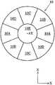
도 5는 도 1의 편광 변환 소자의 구성을 개략적으로 나타내는 도면이다. 또한, 도 6은 수정의 선광성에 대해서 설명하는 도면이다. 또한, 도 7은 편광 변환 소자의 작용에 의해 원주 방향 편광 상태로 설정된 윤대 형상의 2차 광원을 개략적으로 나타내는 도면이다. 본 실시예에 따른 편광 변환 소자(10)는 마이크로 플라이아이 렌즈(11)의 바로 앞에, 즉 조명 광학 장치(1~PL)의 동공 또는 그 근방에 배치되어 있다. 따라서, 윤대 조명의 경우, 편광 변환 소자(10)에는 광축 AX를 중심으로 한 거의 윤대 형상의 단면을 갖는 광속이 입사하게 된다.Fig. 5 is a view schematically showing a configuration of the polarization conversion element of Fig. 1. Fig. 6 is a diagram for explaining the optical rotation of quartz. 7 is a diagram schematically showing a secondary light source of a ring shape set in the circumferential polarization state by the action of the polarization conversion element. The
도 5를 참조하면, 편광 변환 소자(10)는 전체적으로 광축 AX를 중심으로 한 윤대 형상의 유효 영역을 갖고, 이 윤대 형상의 유효 영역은 광축 AX를 중심으로 한 원주 방향으로 등분할된 8개의 부채꼴 형상의 기본 소자에 의해 구성되어 있다. 이들 8개의 기본 소자에 있어서, 광축 AX를 사이에 두고서 대향하는 1쌍의 기본 소자는 서로 동일한 특성을 갖는다. 즉, 8개의 기본 소자는 광의 투과 방향(Y방향)을 따른 두께(광축 방향의 길이)가 서로 상이한 4종류의 기본 소자(10A~10D)를 2개씩 포함하고 있다.5, the
구체적으로는, 제 1 기본 소자(10A)의 두께가 가장 크고, 제 4 기본 소자(10D)의 두께가 가장 작고, 제 2 기본 소자(10B)의 두께는 제 3 기본 소자(10C)의 두께보다도 크게 설정되어 있다. 그 결과, 편광 변환 소자(10)의 한쪽 면(예를 들면, 입사면)은 평면 형상이지만, 다른쪽 면(예를 들면, 사출면)은 각 기본 소자(10A~10D)의 두께 차이에 의해 요철 형상으로 되어 있다. 또한, 편광 변환 소자(10)의 양쪽면(입사면 및 사출면)을 모두 요철 형상으로 형성할 수도 있다.More specifically, the thickness of the first
또한, 본 실시예에서는, 각 기본 소자(10A~10D)가 선광성을 갖는 광학 재료인 결정 재료로서의 수정에 의해 구성되고, 각 기본 소자(10A~10D)의 결정 광학축이 광축 AX와 거의 일치, 즉 입사광의 진행 방향과 거의 일치하도록 설정되어 있다. 이하, 도 6을 참조하여, 수정의 선광성에 대해서 간단하게 설명한다. 도 6을 참조하면, 두께 d의 수정으로 이루어지는 평행 평면판 형상의 광학 부재(100)가, 그 결정 광학축과 광축 AX가 일치하도록 배치되어 있다. 이 경우, 광학 부재(100)의 선광성에 의해, 입사한 직선 편광의 편광 방향이 광축 AX 둘레로 θ만큼 회전한 상태로 사출된다.In this embodiment, each of the
이 때, 광학 부재(100)의 선광성에 의한 편광 방향의 회전각(선광 각도) θ는, 광학 부재(100)의 두께 d와 수정의 선광성 ρ에 의해, 다음의 식(a)로 표현된다.At this time, the rotation angle (optical rotation angle)? Of the polarization direction due to the optical rotation of the

일반적으로, 수정의 선광성 ρ은 파장 의존성(사용광의 파장에 의존하여 선광성의 값이 상이한 성질: 선광 분산)이 있으며, 구체적으로는 사용광의 파장이 짧아지면 커지는 경향이 있다. 「응용 광학 Ⅱ」의 제 167페이지의 기술에 따르면, 250.3㎚의 파장을 갖는 광에 대한 수정의 선광성 ρ은 153.9°/㎜이다.Generally, the optical rotation coefficient ρ of the quartz crystal has a wavelength dependency (a property that the value of the optical rotation is different depending on the wavelength of the used light: optical bright dispersion), and specifically tends to become larger as the wavelength of the used light becomes shorter. According to the technique of page 167 of " Applied Optics II ", the roundness rho of the crystal for light having a wavelength of 250.3 nm is 153.9 DEG / mm.
본 실시예에 있어서, 제 1 기본 소자(10A)는, Z방향으로 편광 방향을 갖는 직선 편광의 광이 입사한 경우, Z방향을 Y축 둘레로 +180° 회전시킨 방향, 즉 Z방향으로 편광 방향을 갖는 직선 편광의 광을 사출하도록 두께 dA가 설정되어 있다. 따라서, 이 경우, 도 7에 나타내는 윤대 형상의 2차 광원(31) 중, 1쌍의 제 1 기본 소자(10A)의 선광 작용을 받은 광속이 형성하는 1쌍의 원호 형상 영역(31A)을 통과하는 광속의 편광 방향은 Z방향으로 된다.In the present embodiment, when linearly polarized light having a polarization direction in the Z direction is incident, the first
제 2 기본 소자(10B)는, Z방향으로 편광 방향을 갖는 직선 편광의 광이 입사한 경우, Z방향을 Y축 둘레로 +135° 회전시킨 방향, 즉 Z방향을 Y축 둘레로 -45° 회전시킨 방향으로 편광 방향을 갖는 직선 편광의 광을 사출하도록 두께 dB가 설정되어 있다. 따라서, 이 경우, 도 7에 나타내는 윤대 형상의 2차 광원(31) 중, 1쌍의 제 2 기본 소자(10B)의 선광 작용을 받은 광속이 형성하는 1쌍의 원호 형상 영역(31B)을 통과하는 광속의 편광 방향은 Z방향을 Y축 둘레로 -45° 회전시킨 방향으로 된다.When the light of the linearly polarized light having the polarization direction in the Z direction is incident, the second
제 3 기본 소자(10C)는, Z방향으로 편광 방향을 갖는 직선 편광의 광이 입사한 경우, Z방향을 Y축 둘레로 +90° 회전시킨 방향, 즉 X방향으로 편광 방향을 갖는 직선 편광의 광을 사출하도록 두께 dC가 설정되어 있다. 따라서, 이 경우, 도 7에 나타내는 윤대 형상의 2차 광원(31) 중, 1쌍의 제 3 기본 소자(10C)의 선광 작용을 받은 광속이 형성하는 1쌍의 원호 형상 영역(31C)을 통과하는 광속의 편광 방향은 X방향으로 된다.When the linearly polarized light having the polarization direction in the Z direction is incident, the third
제 4 기본 소자(10D)는, Z방향으로 편광 방향을 갖는 직선 편광의 광이 입사한 경우, Z방향을 Y축 둘레로 +45° 회전시킨 방향으로 편광 방향을 갖는 직선 편광의 광을 사출하도록 두께 dD가 설정되어 있다. 따라서, 이 경우, 도 7에 나타내는 윤대 형상의 2차 광원(31) 중, 1쌍의 제 4 기본 소자(10D)의 선광 작용을 받은 광속이 형성하는 1쌍의 원호 형상 영역(31D)을 통과하는 광속의 편광 방향은 Z방향을 Y축 둘레로 +45° 회전시킨 방향으로 된다.When the linearly polarized light having the polarization direction in the Z direction is incident, the fourth
또한, 개별적으로 형성된 8개의 기본 소자를 조합하여 편광 변환 소자(10)를 얻을 수도 있고, 혹은 평행 평면판 형상의 수정 기판에 소요의 요철 형상(단차)을 형성함으로써 편광 변환 소자(10)를 얻을 수도 있다. 또한, 편광 변환 소자(10)를 광로로부터 퇴피시키지 않고 통상의 원형 조명을 실행할 수 있도록, 편광 변환 소자(10)의 유효 영역의 직경 방향의 크기의 3/10 이상, 바람직하게는 1/3 이상의 크기를 갖고 또한 선광성을 갖지 않는 원 형상의 중앙 영역(10E)이 마련되어 있다. 여기서, 중앙 영역(10E)은, 예를 들면 석영과 같이 선광성을 갖지 않는 광학 재료에 의해 형성되어 있어도 되고, 단순히 원 형상의 개구이더라도 무방하다. 단, 중앙 영역(10E)은 편광 변환 소자(10)에 필수 요소는 아니다. 또한, 중앙 영역(10E)의 크기는 원주 방향 편광 상태인 영역과 그렇지 않은 영역과의 경계를 결정한다.Alternatively, the
본 실시예에서는, 원주 방향 편광 윤대 조명(윤대 형상의 2차 광원을 통과하는 광속이 원주 방향 편광 상태로 설정된 변형 조명)시에, Z방향으로 편광 방향을 갖는 직선 편광의 광을 편광 변환 소자(10)에 입사시킨다. 그 결과, 마이크로 플라이아이 렌즈(11)의 뒤쪽 초점면 또는 그 근방에는, 도 7에 나타내는 바와 같이, 윤대 형상의 2차 광원(윤대 형상의 조명 동공 분포)(31)가 형성되고, 이 윤대 형상의 2차 광원(31)을 통과하는 광속이 원주 방향 편광 상태로 설정된다. 원주 방향 편광 상태에서는, 윤대 형상의 2차 광원(31)을 구성하는 원호 형상 영역(31A~31D)을 각각 통과하는 광속은, 각 원호 형상 영역(31A~31D)의 원주 방향을 따른 중심 위치에서의 광축 AX를 중심으로 하는 원의 접선 방향과 거의 일치하는 편광 방향을 갖는 직선 편광 상태로 된다.In the present embodiment, light of linearly polarized light having a polarization direction in the Z direction is converted into light in the polarization conversion element (the light flux passing through the secondary light source in the annular shape is set to the circumferentially polarized state) 10. As a result, a ring-shaped secondary light source (annular illumination pupil distribution) 31 is formed at or near the rear focal plane of the micro fly's
이렇게 해서, 본 실시예에서는, 개구 조리개에 있어서 큰 광량 손실이 발생하는 종래 기술과는 상이하게, 편광 변환 소자(10)의 선광 작용에 의해, 광량 손실을 실질적으로 발생시키지 않고, 원주 방향 편광 상태의 윤대 형상의 2차 광원(31)을 형성할 수 있다. 환언하면, 본 실시예의 조명 광학 장치에서는, 광량 손실을 양호하게 억제하면서, 원주 방향 편광 상태의 윤대 형상의 조명 동공 분포를 형성할 수 있다. 또한, 본 실시예에서는, 광학 소자의 편광 작용을 이용하고 있기 때문에, 편광 변환 소자 자체의 제조가 극히 용이하고, 전형적으로는 각 기본 소자의 두께 공차를 극히 완만하게 설정할 수 있다고 하는 우수한 효과를 나타낸다.In this way, in the present embodiment, unlike the prior art in which a large amount of light loss occurs in the aperture diaphragm, the light conversion efficiency of the
또한, 원주 방향 편광 상태의 윤대 형상의 조명 동공 분포에 근거하는 원주 방향 편광 윤대 조명에서는, 최종적인 피조사면으로서의 웨이퍼 W에 조사되는 광이 S편광을 주성분으로 하는 편광 상태로 된다. 여기서, S편광이란, 입사면에 대해서 수직한 방향으로 편광 방향을 갖는 직선 편광(입사면에 수직한 방향으로 전기 벡터가 진동하고 있는 편광)인 것이다. 단, 입사면이란, 광이 매질의 경계면(피조사면:웨이퍼 W의 표면)에 도달했을 때에, 그 점에서의 경계면의 법선과 광의 입사 방향을 포함하는 면으로서 정의된다.In the circumferentially polarized annular illumination based on the annular illumination pupil distribution in the circumferentially polarized state, the light to be irradiated on the wafer W as the final irradiated surface becomes a state of polarization mainly composed of S polarized light. Here, the S-polarized light is linearly polarized light (polarized light in which the electric vector is oscillated in the direction perpendicular to the incident surface) having a polarization direction in a direction perpendicular to the incident surface. Note that the incident surface is defined as a surface including the normal line of the boundary surface at that point and the incident direction of light when the light reaches the boundary surface (surface to be irradiated: wafer W) of the medium.
그 결과, 원주 방향 편광 윤대 조명에서는, 투영 광학계의 광학 성능(초점 심도 등)의 향상을 도모할 수 있어, 웨이퍼(감광성 기판) 위에 있어서 높은 콘트라스트의 마스크 패턴 상(像)을 얻을 수 있다. 즉, 본 실시예의 노광 장치에서는, 광량 손실을 양호하게 억제하면서 원주 방향 편광 상태의 윤대 형상의 조명 동공 분포를 형성할 수 있는 조명 광학 장치를 이용하고 있으므로, 적절한 조명 조건에 근거하여 미세 패턴을 충실하게 또한 높은 스루풋으로 전사할 수 있다.As a result, in the circumferentially polarized annular illumination, the optical performance (depth of focus, etc.) of the projection optical system can be improved, and a mask pattern image of high contrast can be obtained on the wafer (photosensitive substrate). That is, in the exposure apparatus of the present embodiment, since the illumination optical apparatus capable of forming the annular illumination pupil distribution in the circumferential polarization state while satisfactorily suppressing the light amount loss is used, the fine pattern is faithfully And can also be transferred with high throughput.
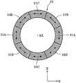
그런데, 본 실시예에서는, X방향으로 편광 방향을 갖는 직선 편광의 광을 편광 변환 소자(10)에 입사시킴으로써, 도 8에 나타내는 바와 같이 윤대 형상의 2차 광원(32)을 통과하는 광속을 직경 방향 편광 상태로 설정하고, 직경 방향 편광 윤대 조명(윤대 형상의 2차 광원을 통과하는 광속이 직경 방향 편광 상태로 설정된 변형 조명)을 실행할 수 있다. 직경 방향 편광 상태에서는, 윤대 형상의 2차 광원(32)을 구성하는 원호 형상 영역(32A~32D)을 각각 통과하는 광속은, 각 원호 형상 영역(32A~32D)의 원주 방향을 따른 중심 위치에서의 광축 AX를 중심으로 하는 원의 반경 방향과 거의 일치하는 편광 방향을 갖는 직선 편광 상태로 된다.Incidentally, in this embodiment, light of a linearly polarized light having a polarization direction in the X direction is made incident on the
직경 방향 편광 상태의 윤대 형상의 조명 동공 분포에 근거하는 직경 방향 편광 윤대 조명에서는, 최종적인 피조사면으로서의 웨이퍼 W에 조사되는 광이 P편광을 주성분으로 하는 편광 상태로 된다. 여기서, P편광이란, 상술한 바와 같이 정의되는 입사면에 대해서 평행한 방향으로 편광 방향을 갖는 직선 편광(입사면에 평행한 방향으로 전기 벡터가 진동하고 있는 편광)인 것이다. 그 결과, 직경 방향 편광 윤대 조명에서는, 웨이퍼 W에 도포된 레지스트에 있어서의 광의 반사율을 작게 억제하여, 웨이퍼(감광성 기판) 위에 있어서 양호한 마스크 패턴 상을 얻을 수 있다.In the radially polarized annular illumination based on the annular illumination pupil distribution in the radially polarized state, the light irradiated on the wafer W as the final irradiated surface is in a state of polarization mainly composed of P polarized light. Here, the P-polarized light is a linearly polarized light (polarized light in which the electric vector is oscillated in a direction parallel to the incident surface) having a polarization direction in a direction parallel to the incident surface defined as described above. As a result, in the radially polarized annular illumination, the reflectance of the light in the resist coated on the wafer W can be suppressed to be small, and a good mask pattern image can be obtained on the wafer (photosensitive substrate).
또한, 상술한 실시예에서는, 편광 변환 소자(10)에 입사하는 광속을, Z방향으로 편광 방향을 갖는 직선 편광 상태와 X방향으로 편광 방향을 갖는 직선 편광 상태 사이에서 전환함으로써, 원주 방향 편광 윤대 조명과 직경 방향 편광 윤대 조명을 실현하고 있다. 그러나, 이에 한정되지 않고, 예를 들면 Z방향 또는 X방향으로 편광 방향을 갖는 직선 편광 상태의 입사 광속에 대해서, 편광 변환 소자(10)를 도 5에 나타내는 제 1 상태와 광축 AX 둘레로 90°만큼 회전시킨 제 2 상태 사이에서 전환함으로써, 원주 방향 편광 윤대 조명과 직경 방향 편광 윤대 조명을 실현할 수도 있다.In the embodiment described above, the light beam incident on the
또한, 상술한 실시예에서는, 마이크로 플라이아이 렌즈(11) 바로 앞에 편광 변환 소자(10)를 배치하고 있다. 그러나, 이에 한정되지 않고, 일반적으로 조명 광학 장치(1~PL)의 동공 또는 그 근방에, 예를 들면 투영 광학계 PL의 동공 또는 그 근방이나, 결상 광학계(15)의 동공 또는 그 근방이나, 원추 액시콘계(8)의 바로 앞(어포컬 렌즈(6)의 동공 또는 그 근방) 등에 편광 변환 소자(10)를 배치할 수도 있다.In the above-described embodiment, the
단, 투영 광학계 PL 중이나 결상 광학계(15) 중에 편광 변환 소자(10)를 배치하면, 편광 변환 소자(10)의 소요의 유효 직경이 커지기 쉽기 때문에, 고품질이며 큰 수정 기판을 얻는 것이 곤란한 현상을 생각하면 그다지 바람직하지 않다. 또한, 원추 액시콘계(8)의 바로 앞에 편광 변환 소자(10)를 배치하면, 편광 변환 소자(10)의 소요의 유효 직경을 작게 억제할 수 있지만, 최종적인 피조사면인 웨이퍼 W까지의 거리가 길고, 그 사이의 광로중에 렌즈의 반사 방지 코팅이나 미러의 반사막과 같이 편광 상태를 변화시키는 요소가 개재하기 쉽기 때문에 그다지 바람직하지 않다. 덧붙여서 말하면, 렌즈의 반사 방지 코팅이나 미러의 반사막에서는, 편광 상태(P편광과 S편광)나 입사 각도에 따라서 반사율에 차가 생기기 쉽고, 나아가서는 광의 편광 상태가 변화하기 쉽다.However, if the
또한, 상술한 실시예에서는, 편광 변환 소자(10)가 적어도 한쪽 면(예를 들면, 사출면)이 요철 형상으로 형성되고, 나아가서는 편광 변환 소자(10)가 원주 방향으로 이산적(불연속적)으로 변화하는 두께 분포를 갖는다. 그러나, 이에 한정되지 않고, 편광 변환 소자(10)가 원주 방향으로 거의 불연속적으로 변화하는 두께 분포를 갖도록, 편광 변환 소자(10)의 적어도 한쪽 면(예를 들면, 사출면)을 곡면 형상으로 형성할 수도 있다.In the embodiment described above, at least one surface (for example, an exit surface) of the
또한, 상술한 실시예에서는, 윤대 형상의 유효 영역의 8분할에 대응하는 8개의 부채꼴 형상의 기본 소자에 의해 편광 변환 소자(10)를 구성하고 있다. 그러나, 이에 한정되지 않고, 예를 들면 원 형상의 유효 영역의 8분할에 대응하는 8개의 부채꼴 형상의 기본 소자에 의해, 혹은 원 형상 또는 윤대 형상의 유효 영역의 4분할에 대응하는 4개의 부채꼴 형상의 기본 소자에 의해, 혹은 원 형상 또는 윤대 형상의 유효 영역의 16분할에 대응하는 16개의 부채꼴 형상의 기본 소자에 의해 편광 변환 소자(10)를 구성할 수도 있다. 즉, 편광 변환 소자(10)의 유효 영역의 형상, 유효 영역의 분할 수(기본 소자의 수) 등에 대해서 다양한 변형예가 가능하다.Further, in the above-described embodiment, the
또한, 상술한 실시예에서는, 수정을 이용하여 각 기본 소자(10A~10D)를(나아가서는, 편광 변환 소자(10)를) 형성하고 있다. 그러나, 이에 한정되지 않고, 선광성을 갖는 다른 적당한 광학 재료를 이용하여 각 기본 소자를 형성할 수도 있다. 이 경우, 사용 파장의 광에 대해서 100°/㎜ 이상의 선광능을 갖는 광학 재료를 이용하는 것이 바람직하다. 즉, 선광능이 작은 광학 재료를 이용하면, 편광 방향의 소요 회전각을 얻기 위해서 필요한 두께가 지나치게 커져, 광량 손실의 원인으로 되기 때문에 바람직하지 않다.In the embodiment described above, the
또한, 상술한 실시예에 있어서, 편광 변환 소자(10)를 조명 광로에 대해서 고정적으로 마련했지만, 이 편광 변환 소자(10)를 조명 광로에 대해서 삽입 탈착 가능하게 마련해도 된다. 또한, 상술한 실시예에서는, 웨이퍼 W에 대한 S편광과 윤대 조명을 조합한 예를 나타냈지만, 웨이퍼 W에 대한 S편광과 2극이나 4극 등의 다극 조명 및 원형 조명과 조합해도 무방하다. 또한, 상술한 실시예에 있어서, 마스크 M으로의 조명 조건이나 웨이퍼 W로의 결상 조건(개구수나 수차 등)은, 예를 들면 마스크 M의 패턴의 종류 등에 따라서 자동적으로 설정할 수 있다.In the above-described embodiment, the
도 9는 복수의 편광 변환 소자를 교환 가능하게 마련한 변형예를 나타낸다. 또한, 도 9의 변형예는 도 1에 나타낸 실시예와 유사한 구성을 갖지만, 복수의 편광 변환 소자를 교환 가능하게 하는 터릿(10T)을 갖는 점에서 상이하다.Fig. 9 shows a modified example in which a plurality of polarization conversion elements are exchangeable. 9 is similar to the embodiment shown in Fig. 1, but differs in that it has a
도 10은 도 9에서의 교환 기구로서의 터릿(10T)에 탑재된 복수 종류의 편광 변환 소자(10a~10e)를 나타내는 도면이다. 도 9 및 도 10에 나타낸 바와 같이, 이 변형예에서는, 광축 AX와 평행한 방향을 축으로 해서 회전 가능한 터릿(10T) 위에 복수 종류의 편광 변환 소자(10a~10e)를 마련하고, 터릿(10T)의 회전 동작에 의해 이들 복수 종류의 편광 변환 소자(10a~10e)를 교환 가능하게 하고 있다. 또한, 도 9에서는 복수 종류의 편광 변환 소자(10a~10c) 중, 편광 변환 소자(10a, 10b)만을 도시하고 있다. 또한, 편광 변환 소자의 교환 기구로서는 터릿(10T)에는 한정되지 않고, 예를 들면 슬라이더라도 무방하다.10 is a view showing a plurality of kinds of
도 11은 복수 종류의 편광 변환 소자(10a~10e)의 각각의 구성을 나타내는 도면이다. 도 11(a)에서, 제 1 편광 변환 소자(10a)는 도 5에 나타낸 실시예의 편광 변환 소자(10)와 동일한 구성을 갖는다. 도 11(b)에서, 제 2 편광 변환 소자(10b)는 도 11(a)에 나타낸 편광 변환 소자(10a)와 유사한 구성을 갖지만, 중앙 영역(10E)에 편광 해소 부재(104c)가 마련되어 있는 점에서 상이하다. 이 편광 해소 부재(104c)는 도 1에 나타낸 디폴라라이저(4c)와 마찬가지의 구성을 갖고, 입사하는 직선 편광의 광을 비편광 상태의 광으로 변환하는 기능을 갖는다.11 is a diagram showing the configuration of each of the plural types of
도 11(c)에서, 제 3 편광 변환 소자(10c)는 도 11(a)에 나타낸 편광 변환 소자(10a)와 유사한 구성을 갖지만, 중앙 영역(10E)의 크기가 크게 되어 있는 점(제 1~제 4 기본 소자(10A~10D)의 폭이 좁게 되어 있는 점)에서 상이하다. 또한, 도 11(d)에서, 제 4 편광 변환 소자(10d)는 도 11(c)에 나타낸 편광 변환 소자(10c)와 유사한 구성을 갖지만, 중앙 영역(10E)에 편광 해소 부재(104c)가 마련되어 있는 점에서 상이하다.11 (c), the third
도 11(c)에서, 제 5 편광 변환 소자(10e)는 8개의 기본 소자가 아니라, 6개의 기본 소자(10C, 10F, 10G)를 조합해서 구성되어 있다. 제 5 편광 변환 소자(10e)는 전체적으로 광축 AX를 중심으로 한 윤대 형상의 유효 영역을 갖고, 이 윤대 형상의 유효 영역은 광축 AX를 중심으로 한 원주 방향으로 등분할된 6개의 부채꼴 형상의 기본 소자(10C, 10F, 10G)에 의해 구성되어 있다. 이들 6개의 기본 소자(10C, 10F, 10G)에 있어서, 광축 AX를 사이에 두고서 대향하는 1쌍의 기본 소자는 서로 동일한 특성을 갖는다. 즉, 6개의 기본 소자(10C, 10F, 10G)는 광의 투과 방향(Y방향)을 따른 두께(광축 방향의 길이)가 서로 상이한 3종류의 기본 소자(10C, 10F, 10G)를 2개씩 포함하고 있다.In Fig. 11 (c), the fifth
여기서, 기본 소자(10C)는 도 7에 나타낸 제 3 기본 소자(10C)와 동일한 기능을 갖는 부재이기 때문에, 그 기능의 설명을 생략한다. 기본 소자(10F)는 Z방향으로 편광 방향을 갖는 직선 편광이 입사한 경우, Z방향을 Y축 둘레로 +150° 회전시킨 방향, 즉 Z방향을 Y축 둘레로 -30° 회전시킨 방향으로 편광 방향을 갖는 직선 편광의 광을 사출하도록 두께 dF가 설정되어 있다. 기본 소자(10G)는 Z방향으로 편광 방향을 갖는 직선 편광이 입사한 경우, Z방향을 Y축 둘레로 +30° 회전시킨 방향으로 편광 방향을 갖는 직선 편광의 광을 사출하도록 두께 dG가 설정되어 있다. 또한, 중앙 영역(10E) 대신에 편광 해소 부재(104c)를 마련해도 된다.Here, since the
또한, 도 10으로 되돌아가서, 터릿(10T)에는 편광 변환 소자가 탑재되지 않는 개구부(40)가 마련되어 있고, 원주 방향 편광 조명이 아닌 편광 조명을 실행하는 경우나, 큰 σ값(σ값=조명 광학 장치의 마스크측 개구수/투영 광학계의 마스크측 개구수)에 근거하여 비편광 조명을 실행하는 경우에는, 이 개구부(40)가 조명 광로중에 위치한다.10, the
또한, 상술에서는, 터릿(10T)에 탑재되는 편광 변환 소자(10a~10e)의 중앙부에, 원 형상의 개구 또는 선광성을 갖지 않는 재료로 이루어지는 중앙 영역(10E) 혹은 편광 해소 부재(104c)를 마련한 예만 나타냈지만, 중앙 영역(10E) 또는 편광 해소 부재(104c)를 마련하지 않은 편광 변환 소자(부채꼴 형상의 기본 소자로 이루어지는 편광 변환 소자)를 탑재해도 된다.In the above description, a
도 12는 편광 변환 소자의 작용에 의해 원주 방향 편광 상태로 설정된 2차 광원의 일례를 개략적으로 나타내는 도면이다. 또한, 도 12에서는, 이해를 용이하게 하기 위해서 편광 변환 소자도 겹쳐서 도시하고 있다.12 is a view schematically showing an example of a secondary light source set in a circumferential polarization state by the action of a polarization conversion element. In Fig. 12, the polarization conversion elements are also shown overlapping to facilitate understanding.
도 12(a)는 회절 광학 소자(5) 대신에, 파필드(또는, 프라운호퍼 회절 영역)에 8극 형상의 광강도 분포를 형성하는 회절 광학 소자(광속 변환 소자)가 조명 광로에 설치되고, 또한, 편광 변환 소자(10a, 10b)가 조명 광로에 설치된 경우에 있어서의 8극 형상의 2차 광원(33)을 나타내고 있다. 여기서, 8극 형상의 2차 광원(33)을 통과하는 광속이 원주 방향 편광 상태로 설정된다. 원주 방향 편광 상태에서는, 8극 형상의 2차 광원(33)을 구성하는 8개의 원형 영역(33A~33D)을 각각 통과하는 광속이, 이들 8개의 원형 영역(33A~33D)을 연결하는 원의 원주 방향, 즉 이들 8개의 원형 영역(33A~33D)을 연결하는 원의 접선 방향과 거의 일치하는 편광 방향을 갖는 직선 편광 상태로 된다. 또한, 도 12(a)에서는, 8극 형상의 2차 광원(33)을 8개의 원형 영역(33A~33D)으로 구성한 예를 나타냈지만, 8개의 영역의 형상은 원형에만 한정되지 않는다.12 (a), a diffractive optical element (light flux conversion element) for forming an 8-pole light intensity distribution in a far field (or a Fraunhofer diffraction area) is provided in an illumination light path instead of the diffractive
도 12(b)에는, 회절 광학 소자(5) 대신에, 파필드(또는, 프라운호퍼 회절 영역)에 4극 형상의 광강도 분포를 형성하는 회절 광학 소자(광속 변환 소자)가 조명 광로에 설치되고, 또한, 편광 변환 소자(10c, 10d)가 조명 광로에 설치된 경우에 있어서의 4극 형상의 2차 광원(34)을 도시하고 있다. 여기서, 4극 형상의 2차 광원(34)을 통과하는 광속이 원주 방향 편광 상태로 설정된다. 원주 방향 편광 상태에서는, 4극 형상의 2차 광원(34)을 구성하는 4개의 영역(34A, 34C)을 각각 통과하는 광속이, 이들 4개의 영역(34A, 34C)을 연결하는 원의 원주 방향, 즉 이들 4개의 영역(34A, 34C)을 연결하는 원의 접선 방향과 거의 일치하는 편광 방향을 갖는 직선 편광 상태로 된다. 또한, 도 12(b)에서는, 4극 형상의 2차 광원(34)을 4개의 거의 타원 형상의 영역(34A, 34C)으로 구성한 예를 나타냈지만, 4개의 영역의 형상은 거의 타원 형상에만 한정되지 않는다.12B shows a diffractive optical element (light flux conversion element) for forming a quadrupole light intensity distribution in a far field (or a Fraunhofer diffraction area) in place of the diffractive
도 12(c)에는, 회절 광학 소자(5) 대신에, 파필드(또는, 프라운호퍼 회절 영역)에 6극 형상의 광강도 분포를 형성하는 회절 광학 소자(광속 변환 소자)가 조명 광로에 설치되고, 또한, 편광 변환 소자(10e)가 조명 광로에 설치된 경우에 있어서의 6극 형상의 2차 광원(35)을 나타내고 있다. 여기서, 6극 형상의 2차 광원(35)을 통과하는 광속이 원주 방향 편광 상태로 설정된다. 원주 방향 편광 상태에서는, 6극 형상의 2차 광원(35)을 구성하는 6개의 영역(35C, 35F, 35G)을 각각 통과하는 광속이, 이들 6개의 영역(35C, 35F, 35G)을 연결하는 원의 원주 방향, 즉 이들 6개의 영역(35C, 35F, 35G)을 연결하는 원의 접선 방향과 거의 일치하는 편광 방향을 갖는 직선 편광 상태로 된다. 또한, 도 12(c)에서는, 6극 형상의 2차 광원(35)을 4개의 거의 사다리꼴 형상의 영역(35C, 35F, 35G)으로 구성한 예를 나타냈지만, 6개의 영역의 형상은 거의 사다리꼴 형상에만 한정되지 않는다.12 (c), a diffraction optical element (light flux conversion element) for forming a six-pole light intensity distribution in a far field (or a Fraunhofer diffraction area) is provided in the illumination light path instead of the diffraction
또한, 상술한 실시예 및 변형예에서는, 편광 변환 소자가 광축 둘레에 고정되어 있었지만, 편광 변환 소자를 광축 둘레로 회전시켜도 된다. 도 13은 광축 AX 둘레로 회전 가능하게 마련된 편광 변환 소자(10f)의 구성을 개략적으로 나타내는 도면이다.Further, in the above-described embodiment and modified examples, the polarization conversion element is fixed around the optical axis, but the polarization conversion element may be rotated around the optical axis. Fig. 13 is a view schematically showing the configuration of the
도 13에서, 편광 변환 소자(10f)는 4개의 기본 소자(10A, 10C)를 조합해서 구성되어 있다. 편광 변환 소자(10f)는 전체적으로 광축 AX를 중심으로 한 윤대 형상의 유효 영역을 갖고, 이 윤대 형상의 유효 영역은 광축 AX를 중심으로 한 원주 방향으로 등분할된 4개의 부채꼴 형상의 기본 소자(10A, 10C)에 의해 구성되어 있다. 이들 4개의 기본 소자(10A, 10C)에 있어서, 광축 AX를 사이에 두고서 대향하는 1쌍의 기본 소자는 서로 동일한 특성을 갖는다. 즉, 4개의 기본 소자(10A, 10C)는 광의 투과 방향(Y방향)을 따른 두께(광축 방향의 길이)가 서로 상이한 2종류의 기본 소자(10A, 10C)를 2개씩 포함하고 있다.In Fig. 13, the
여기서, 기본 소자(10A)는 도 7에 나타낸 제 1 기본 소자(10A)와 동일한 기능을 갖는 부재이며, 기본 소자(10C)는 도 7에 나타낸 제 3 기본 소자(10C)와 동일한 기능을 갖는 부재이기 때문에, 그 기능의 설명을 생략한다. 또한, 중앙 영역(10E) 대신에, 편광 해소 부재(104c)를 마련해도 된다.Here, the
이 편광 변환 소자(10f)는 광축 AX를 중심으로 해서 회전 가능하게 되도록 마련되어 있고, 예를 들면 광축 AX를 중심으로 해서 +45° 또는 -45°만큼 회전 가능하게 되어 있다. 도 14는 편광 변환 소자(10f)의 작용에 의해 원주 방향 편광 상태로 설정된 2차 광원의 일례를 개략적으로 나타내는 도면이다. 또한, 도 14에서는, 이해를 용이하게 하기 위해서 편광 변환 소자(10f)도 겹처서 도시하고 있다.The polarized
도 14(a)는 회절 광학 소자(5) 대신에, 파필드(또는, 프라운호퍼 회절 영역)에 2극 형상의 광강도 분포를 형성하는 회절 광학 소자(광속 변환 소자)가 조명 광로에 설치되고, 또한, 편광 변환 소자(10f)가 회전각 0°인 상태(기준 상태)에서 조명 광로에 설치된 경우에 있어서의 2극 형상의 2차 광원(36)((36A))을 나타내고 있다. 여기서는, 2극 형상의 2차 광원(36)((36A))을 통과하는 광속이 종방향 편광 상태로 설정된다.14A, diffractive optical element (light flux conversion element) for forming a bipolar light intensity distribution in a far field (or a Fraunhofer diffractive area) is provided in an illumination light path instead of the diffractive
도 14(b)는 회절 광학 소자(5) 대신에, 파필드(또는, 프라운호퍼 회절 영역)에 4극 형상의 광강도 분포를 형성하는 회절 광학 소자(광속 변환 소자)가 조명 광로에 설치되고, 또한, 편광 변환 소자(10f)가 회전각 0°인 상태(기준 상태)에서 조명 광로에 설치된 경우에 있어서의 4극 형상의 2차 광원(37)을 나타내고 있다. 여기서는, 4극 형상의 2차 광원(37)을 통과하는 광속이 원주 방향 편광 상태로 설정된다. 또한, 도 14(b)에서의 4극 형상의 광강도 분포는 지면내 상하 방향(Z방향) 및 좌우 방향(X방향)으로 국재하고 있다.14 (b), a diffractive optical element (light flux conversion element) for forming a quadrupole light intensity distribution in a far field (or a Fraunhofer diffraction area) is provided in the illumination light path instead of the diffractive
원주 방향 편광 상태에서는, 4극 형상의 2차 광원(37)을 구성하는 4개의 원형 영역(37A, 37C)을 각각 통과하는 광속이, 이들 4개의 원형 영역(37A, 37C)을 연결하는 원의 원주 방향, 즉 이들 4개의 원형 영역(37A, 37C)을 연결하는 원의 접선 방향과 거의 일치하는 편광 방향을 갖는 직선 편광 상태로 된다. 또한, 도 14(b)에서는, 4극 형상의 2차 광원(37)을 4개의 원형 영역(37A, 37C)으로 구성한 예를 나타냈지만, 4개의 영역의 형상은 원형에만 한정되지 않는다.In the circumferential polarization state, the light flux passing through each of the four
도 14(c)는 도 14(b)의 회절 광학 소자 대신에, 파필드(또는, 프라운호퍼 회절 영역)에 지면내 +45°(-135°) 방향 및 지면내 -45°(+135°) 방향으로 국재하는 4극 형상의 광강도 분포를 형성하는 회절 광학 소자(광속 변환 소자)가 조명 광로에 설치되고, 또한 편광 변환 소자(10f)를 회전각 +45° 상태(기준 상태에 대해서 시계 방향으로 45°만큼 회전시킨 상태)로 회전시켜서 조명 광로에 설치한 경우에 있어서의 4극 형상의 2차 광원(38)을 나타내고 있다.14 (c) shows a case in which the + 45 ° (-135 °) direction in the plane and -45 ° (+ 135 °) direction in the plane are added to the far field (or the Fraunhofer diffraction area) instead of the diffractive optical element shown in FIG. (Light flux conversion element) for forming a quadrupole light intensity distribution which is localized in the direction of the polarization axis is provided in the illumination optical path and the
도 14(c)에서는, 편광 상태 전환부(4) 중의 1/2 파장판(4b)을 광축 둘레로 회전시키고, 편광 변환 소자(10f)에 대해서 +45° 방향(-135° 방향)으로 편광 방향을 갖는 직선 편광을 입사시킨다. 여기서, 기본 소자(10A)는 입사한 직선 편광의 편광 방향을 180°±n×180°(n은 정수)만큼 회전시키는 기능을 갖으며, 기본 소자(10C)는 입사한 직선 편광의 편광 방향을 90°±n×180°(n은 정수)만큼 회전시키는 기능을 갖기 때문에, 4극 형상의 2차 광원(38)을 통과하는 광속이 원주 방향 편광 상태로 설정된다.14 (c), the 1/2
도 14(c)에 나타낸 원주 방향 편광 상태에서는, 4극 형상의 2차 광원(38)을 구성하는 4개의 원형 영역(38B, 38D)을 각각 통과하는 광속이, 이들 4개의 원형 영역(38B, 38D)을 연결하는 원의 원주 방향, 즉 이들 4개의 원형 영역(38B, 38D)을 연결하는 원의 접선 방향과 거의 일치하는 편광 방향을 갖는 직선 편광 상태로 된다. 또한, 도 14(c)에서는, 4극 형상의 2차 광원(38)을 4개의 원형 영역(38B, 38D)으로 구성한 예를 나타냈지만, 4개의 영역의 형상은 원형에만 한정되지 않는다.In the circumferential direction polarization state shown in Fig. 14C, the light flux passing through each of the four
이와 같이, 편광 상태 전환부(4)의 편광 방향의 변경 동작과, 편광 변환 소자(10f)의 회전 동작에 의해, +45°(-135°) 방향 및 -45°(+135°) 방향으로 국재하는 4극 형상의 2차 광원이더라도, 0°(+180°) 방향 및 90°(270°), 즉 종횡 방향으로 국재하는 4극 형상의 2차 광원이더라도, 0°(+180°) 방향 또는 90°(270°), 즉 종횡 방향으로 국재하는 2극 형상의 2차 광원이더라도, 원주 방향 편광 상태를 실현할 수 있다.As described above, the polarization direction changing operation of the polarization
또한, 광축 AX를 중심으로 한 원주 방향으로 등분할된 8개의 부채꼴 형상의 기본 소자로 구성되는 편광 변환 소자를, 광축 AX 둘레로 회전 가능하게 해도 좋다. 도 15(a)에 나타내는 바와 같이, 예를 들면 상기 8분할의 기본 소자로 이루어지는 편광 변환 소자(예를 들면, 편광 변환 소자(10a))를 +45°만큼 광축 AX 둘레로 회전시키면, 8극 형상의 2차 광원(39)을 구성하는 8개의 원형 영역(39A~39D)을 각각 통과하는 광속이, 이들 8개의 원형 영역(39A~39D)을 연결하는 원의 원주 방향(이들 8개의 원형 영역(39~39D)을 연결하는 원의 접선 방향)에 대해서 -45°만큼 회전된 편광 방향을 갖는 직선 편광 상태로 된다.Further, the polarization conversion element composed of eight basic-shaped element elements equally divided in the circumferential direction about the optical axis AX may be rotatable around the optical axis AX. As shown in Fig. 15 (a), for example, when the polarization conversion element (for example, the
또한, 도 15(b)에 나타내는 바와 같이, 8극 형상의 2차 광원을 구성하는 8개의 원형 영역을 각각 통과하는 광속이, 이들 8개의 원형 영역을 연결하는 원의 원주 방향(이들 8개의 원형 영역을 연결하는 원의 접선 방향)에 대해서 +45°만큼 회전된 방향으로 긴 축을 갖는 타원 편광인 경우에는, 도 15(a)에 나타낸 바와 같이 편광 변환 소자(예를 들면, 편광 변환 소자(10a))를 +45°만큼 광축 AX 둘레로 회전시킴으로써, 도 15(c)에 나타내는 바와 같이, 대략 원주 방향 편광 상태를 얻을 수 있다.Further, as shown in Fig. 15 (b), the light flux passing through each of the eight circular regions constituting the quadratic light source of the eight-pole shape is divided into a circle circumferential direction of these eight circular regions Polarized light having a long axis in the direction rotated by + 45 degrees with respect to the direction of the tangential line of the circle connecting the
도 16은 편광 변환 소자를 조명 광학 장치의 동공 근방의 위치 중, 원추 액시콘계(8)의 바로 앞의 위치(입사측 근방의 위치)에 배치한 예를 나타낸다. 이 도 16의 예에서는, 줌 렌즈계(9)의 변배 작용에 의해서, 마이크로 플라이아이 렌즈(11)의 입사면에 투영되는 중앙 영역(10E)의 상(像)의 크기와, 마이크로 플라이아이 렌즈(11)의 입사면에 투영되는 각 기본 소자(10A~10D)의 상의 크기가 변경되고, 원추 액시콘계(8)의 동작에 의해서, 마이크로 플라이아이 렌즈(11)의 입사면에 투영되는 각 기본 소자(10A~10D)의 상에서의 광축 AX를 중심으로 하는 반경 방향의 폭이 변경된다.16 shows an example in which the polarized light conversion element is disposed at a position in the vicinity of the pupil of the illumination optical apparatus and at a position immediately before the conical axicon system 8 (near the incidence side). 16, the size of the image of the
따라서, 도 16에 나타낸 변형예와 같이 중앙 영역(10E)(또는, 편광 해소 부재(104c))을 갖는 편광 변환 소자를, 변배 작용을 갖는 광학계(줌 렌즈(9))보다도 광원 쪽에 마련하는 경우에는, 중앙 영역(10E)이 차지하는 영역이 줌 렌즈(9)의 변배에 의해서 변경되는 것을 고려하여, 중앙 영역(10E)의 크기를 정하면 된다.Therefore, when the polarization conversion element having the
또한, 도 16에 나타낸 변형예와 같이, 중앙 영역(10E)(또는, 편광 해소 부재(104c))을 갖는 편광 변환 소자를, 윤대비를 변경하는 작용을 갖는 광학계(원추 액시콘계(8))보다도 광원 쪽에 마련하는 경우에는, 도 17에 나타내는 바와 같이, 이하의 조건식(1) 및 (2) 중 적어도 한쪽의 조건식을 만족하는 것이 바람직하다.16, the polarization conversion element having the


단,only,
10in: 편광 변환 소자(10)의 중앙 영역(10E)의 유효 반경,10in: Effective radius of the
10out : 편광 변환 소자(10)의 외측 유효 반경,10out: outer effective radius of the
ΔA: 윤대비를 변경하는 작용을 갖는 광학계를 통과한 광속의 내측 반경의 증가분ΔA: Increase in the inner radius of the light beam passing through the optical system having the action of changing the ratio
이다.to be.
여기서, 조건식(1)을 만족하지 않는 경우에는, 편광 변환 소자(10)에 의해서 원주 방향 편광 상태로 변환되는 윤대 형상의 영역의 폭이 좁아지고, 작은 윤대비에 근거하여 윤대 형상 또는 다극 형상 2차 광원에 의한 원주 방향 편광 조명을 달성할 수 없게 되기 때문에 바람직하지 않다. 또한, 조건식(2)를 만족하지 않는 경우에는, 편광 변환 소자(10)의 중앙 영역을 통과할 수 있는 광속의 직경이 현저하게 작아지고, 예를 들면 당해 편광 변환 소자(10)를 조명 광로로부터 분리하지 않고, 편광 상태를 바꾸지 않고서 작은 σ 조명을 할 수 없게 되기 때문에 바람직하지 않다.Here, when the condition (1) is not satisfied, the width of the zone of the annular shape which is converted into the circumferential polarization state by the
또한, 도 18에 나타내는 바와 같이, 편광 변환 소자를 조명 광학 장치의 동공 근방의 위치 중, 마이크로 플라이아이 렌즈(11)보다도 마스크 쪽의 위치, 구체적으로는 마스크 블라인드(14)의 상을 마스크 위에 투영하는 결상 광학계(15)의 동공 위치의 근방에 마련해도 된다. 도 16 및 도 18에 나타낸 실시예에 있어서도, 도 9 내지 도 11의 실시예와 마찬가지로 복수의 편광 변환 소자를 교환 가능하게 해도 된다.18, the position of the polarizing conversion element in the vicinity of the pupil of the illumination optical apparatus is located at a position closer to the mask than the micro fly's
또한, 상술한 실시예에 있어서, 편광 변환 소자(10)보다도 웨이퍼 W 쪽의 광학계(조명 광학계나 투영 광학계)가 편광 수차(지연(retardation))를 갖고 있는 경우에는, 이 편광 수차에 기인해서 편광 방향이 변화하는 일이 있다. 이 경우에는, 이들 광학계의 편광 수차의 영향을 고려한 후에, 편광 변환 소자(10)에 의해 선회되는 편광면의 방향을 설정하면 된다. 또한, 편광 변환 소자(10)보다도 웨이퍼 W 쪽의 광로중에 반사 부재가 배치되어 있는 경우, 이 반사 부재에서 반사된 편광 방향마다 위상차가 생기는 일이 있다. 이 때, 반사면의 편광 특성에 기인하는 광속의 위상차를 고려한 후에, 편광 변환 소자(10)에 의해 선회되는 편광면의 방향을 설정하면 된다.In the above embodiment, when the optical system (illumination optical system or projection optical system) on the wafer W side has a polarization aberration (retardation) rather than the
다음에, 편광 상태의 평가 수법의 실시예에 대해서 설명한다. 본 실시예에서는, 감광성 기판으로서의 웨이퍼 W를 유지하는 웨이퍼 스테이지(기판 스테이지)의 옆쪽에 부착 가능한 웨이퍼면 편광 모니터(90)를 이용하여, 감광성 기판으로서의 웨이퍼 W에 도달하는 광속의 편광 상태를 검출한다. 또한, 웨이퍼면 편광 모니터(90)는 웨이퍼 스테이지 내에 마련되어도 무방하고, 당해 웨이퍼 스테이지와는 별도의 계측 스테이지에 마련되어도 무방하다.Next, an example of the evaluation method of the polarization state will be described. In this embodiment, the polarization state of the light beam reaching the wafer W as the photosensitive substrate is detected by using the wafer-side polarization monitor 90 attachable to the side of the wafer stage (substrate stage) holding the wafer W as the photosensitive substrate . Further, the wafer-surface polarization monitor 90 may be provided in the wafer stage, and it may be provided in a measurement stage separate from the wafer stage.
도 19는 웨이퍼 W를 조명하는 광의 편광 상태 및 광강도를 검출하기 위한 웨이퍼면 편광 모니터(90)의 개략적인 구성을 나타내는 도면이다. 도 19에 나타내는 바와 같이, 웨이퍼면 편광 모니터(90)는 웨이퍼 W의 위치 또는 그 근방에 위치 결정 가능한 핀홀 부재(91)를 구비하고 있다. 핀홀 부재(91)의 핀홀(91a)을 통과한 광은, 투영 광학계 PL의 상면(像面) 위치 또는 그 근방이 앞쪽 초점 위치로 되도록 배치되어 있는 콜리메이트 렌즈(92)를 거쳐서 거의 평행한 광속으로 되어, 반사경(93)에서 반사된 후, 릴레이 렌즈계(94)에 입사한다. 릴레이 렌즈계(94)를 거친 거의 평행한 광속은, 위상 시프터(移相子)로서의 λ/4판(95) 및 편광자로서의 편광 빔 스플리터(96)를 거친 후, 2차원 CCD(97)의 검출면(97a)에 도달한다. 여기서, 2차원 CCD(97)의 검출면(97a)은 투영 광학계 PL의 사출 동공과 광학적으로 거의 공액, 나아가서는 조명 광학 장치의 조명 동공면과 광학적으로 거의 공액으로 되어 있다.19 is a diagram showing a schematic configuration of a wafer surface polarization monitor 90 for detecting the polarization state and light intensity of light illuminating the wafer W. Fig. 19, the wafer surface polarized
λ/4판(95)은 광축을 중심으로 해서 회전 가능하게 구성되어 있고, 이 λ/4판(95)에는, 그 광축을 중심으로 한 회전각을 설정하기 위한 설정부(98)가 접속되어 있다. 이렇게 해서, 웨이퍼 W에 대한 조명광의 편광도가 0이 아닌 경우에는, 설정부(98)를 거쳐서 λ/4판(95)을 광축 둘레로 회전시킴으로써 2차원 CCD(97)의 검출면(97a)에 있어서의 광강도 분포가 변화한다. 따라서, 웨이퍼면 편광 모니터(90)에서는, 설정부(98)를 이용하여 λ/4판(95)을 광축 둘레로 회전시키면서 검출면(97a)에 있어서의 광강도 분포의 변화를 검출하고, 이 검출 결과로부터 회전 위상 시프터법에 의해 조명광의 편광 상태를 측정할 수 있다.The λ / 4
또한, 회전 위상 시프터법에 대해서는, 예를 들면 츠루다 저술, 「광의 연필-광 기술자를 위한 응용 광학」, 주식회사 신기술 커뮤니케이션 등에 상세하게 기재되어 있다. 실제로는, 핀홀 부재(90)(나아가서는, 핀홀(90a))를 웨이퍼면을 따라 2차원적으로 이동시키면서, 웨이퍼면 내의 복수의 위치에 있어서의 조명광의 편광 상태를 측정한다. 이 때, 웨이퍼면 편광 모니터(90)에서는, 2차원적인 검출면(97a)에 있어서의 광강도 분포의 변화를 검출하기 때문에, 이 검출 분포 정보에 근거하여 조명광의 동공 내에 있어서의 편광 상태의 분포를 측정할 수 있다.The rotation phase shifter method is described in detail, for example, in Tsuru-Daishi, "Optical pencil-application optics for optical technicians", New Technology Communication Co., Ltd. and the like. Actually, the polarization state of the illumination light at a plurality of positions in the wafer surface is measured while the pinhole member 90 (and hence the pinhole 90a) is moved two-dimensionally along the wafer surface. At this time, since the wafer surface polarized
또한, 웨이퍼면 편광 모니터(90)에서는, 위상 시프터로서 λ/4판(95) 대신에λ/2판을 이용하는 것도 가능하다. 어떠한 위상 시프터를 이용했다고 하더라도, 편광 상태, 즉 4개의 스토크스(stokes) 파라미터를 측정하기 위해서는, 위상 시프터와 편광자(편광 빔 스플리터(96))와의 광축 둘레의 상대 각도를 바꾸거나, 위상 시프터 또는 편광자를 광로로부터 퇴피시키거나 해서, 적어도 4개의 상이한 상태에서 검출면(97a)에 있어서의 광강도 분포의 변화를 검출할 필요가 있다. 또한, 본 실시예에서는 위상 시프터로서의 λ/4판(95)을 광축 둘레로 회전시켰지만, 편광자로서의 편광 빔 스플리터(96)를 광축 둘레로 회전시켜도 되고, 위상 시프터 및 편광자의 양쪽을 광축 둘레로 회전시켜도 된다. 또한, 이 동작 대신에, 혹은 이 동작에 부가하여, 위상 시프터로서의 λ/4판(95) 및 편광자로서의 편광 빔 스플리터(96) 중 한쪽 또는 양쪽을 광로로부터 삽입 탈착시켜도 된다.In the wafer plane polarization monitor 90, it is also possible to use a? / 2 plate instead of the? / 4
또한, 웨이퍼면 편광 모니터(90)에서는, 반사경(93)의 편광 특성에 의해 광의 편광 상태가 변화해 버리는 경우가 있다. 이 경우, 반사경(93)의 편광 특성은 미리 알 수 있기 때문에, 소요의 계산에 의해서 반사경(93)의 편광 특성의 편광 상태에 대한 영향에 근거해서 웨이퍼면 편광 모니터(90)의 측정 결과를 보정하여, 조명광의 편광 상태를 정확하게 측정할 수 있다. 또한, 반사경에 한정되지 않고, 렌즈 등의 다른 광학 부품에 기인해서 편광 상태가 변화해 버리는 경우에도 마찬가지로 측정 결과를 보정하여, 조명광의 편광 상태를 정확하게 측정할 수 있다.In addition, in the wafer surface polarization monitor 90, the polarization state of the light may change due to the polarization property of the reflecting
이하, 조명광의 동공 내에 있어서의 편광 상태의 분포의 평가에 대해서 구체적으로 설명한다. 먼저, 동공 위의 한 점(또는, 미소 영역)을 통과해서 상면 위의 한 점(미소 영역)에 도달하는 광선의 한개 한개에 대해서 특정 편광도(DSP)를 산출한다. 또한, 이하의 설명에서는, 도 1, 도 16, 도 18에서 이용한 XYZ 좌표계를 이용한다. 상술한 동공 위의 한 점(미소 영역)은 2차원 CCD(97)의 1화소에 대응하고, 상면 위의 한 점(미소 영역)은 핀홀(90a)의 XY 좌표에 대응한다.Hereinafter, the evaluation of the distribution of the polarization states in the pupil of the illumination light will be described in detail. First, a specific degree of polarization (DSP) is calculated for one of the light rays passing through a point (or a minute region) on the pupil and reaching a point (microdomain) on the upper surface. In the following description, the XYZ coordinate system used in Figs. 1, 16, and 18 is used. One point (micro-area) on the pupil corresponds to one pixel of the two-
이 특정 편광도(DSP)는 동공 위의 한 점(또는, 미소 영역)을 통과해서 상면 위의 한 점(미소 영역)에 도달하는 특정 광선에 있어서의 X방향 편광(동공 위에 있어서 X방향으로 진동 방향을 가지는 편광) 성분의 강도를 Ix로 하고, 당해 특정 광선에 있어서의 Y방향 편광(동공 위에 있어서 Y방향으로 진동 방향을 가지는 편광) 성분의 강도를 Iy로 할 때,This specific degree of polarization DSP passes through one point (or microdomain) on the pupil and is converted into X-directional polarized light (in the X direction on the pupil) in a specific ray reaching one point (microdomain) Direction is Ix and the intensity of the Y-direction polarized light (polarized light having a vibration direction in the Y direction on the pupil) component in the specific light ray is Iy,

로 표현된다. 또한, 이 특정 편광도(DSP)는 전강도 S0에 대한 수평 직선 편광강도 마이너스 수직 직선 편광강도 S1(S1/S0)과 동일한 의미이다.Lt; / RTI > Further, a specific polarization (DSP) are also Jeongang is as defined with the vertical straight line horizontal linear polarization intensity minus polarization intensity of the S0S 1 (S 1 / S 0 ).
또한, 동공 위의 한 점(또는, 미소 영역)을 통과해서 상면 위의 한 점(미소 영역)에 도달하는 특정 광선에 있어서의 X방향 편광(동공 위에 있어서 X방향으로 진동 방향을 가지는 편광) 성분의 강도 Ix, 및 당해 특정 광선에 있어서의 Y방향 편광(동공 위에 있어서 Y방향으로 진동 방향을 가지는 편광) 성분의 강도 Iy로부터, 아래 식(4), (5)와 같이, 수평 편광(패턴면 내에서 수평 방향으로 연장한 마스크 패턴의 회절광에 대해서 S편광으로 되는 편광)에 대한 적정 편광율 RSPh, 및 수직 편광(패턴면 내에서 수직 방향으로 연장한 마스크 패턴의 회절광에 대해서 S편광으로 되는 편광)에 대한 적정 편광율 RSPv를 정의할 수 있다.Further, the X-direction polarized light (polarized light having a vibration direction in the X direction on the pupil) in a specific ray passing through a point (or a minute region) on the pupil and reaching a point (minute region) (4) and (5) from the intensity Ix of the specific light beam and the intensity Iy of the Y direction polarized light (polarized light having the vibration direction in the Y direction on the pupil) with respect to the diffracted light of the mask pattern extending in the horizontal direction proper polarization of the polarized light that is S polarized light) ratio RSPh, and vertically polarized light (the pattern surface S polarized with respect to the diffracted light of the mask pattern extending in the vertical direction in the The polarized light RSPv can be defined.


여기서, 이상적인 비편광 조명시에는 RSPh, RSPv는 모두 50%로 되고, 이상적인 수평 편광시에는 RSPh가 100%로 되고, 이상적인 수직 편광시에는 RSPv가 100%로 된다.Here, in the ideal non-polarized illumination, RSPh and RSPv are all 50%, RSPh becomes 100% at ideal horizontal polarization, and RSPv becomes 100% at ideal vertical polarization.
또한, 동공 위의 한 점(또는, 미소 영역)을 통과해서 상면 위의 한 점(미소 영역)에 도달하는 광선의 한개 한개에 대해서, 아래 식(6)~(9)로 편광도 V를 정의할 때, 소정의 유효 광원 영역을 통과해서 상면 위의 한 점(미소 영역)에 도달하는 광선속에 대해서, 아래 식(10)과 같이 평균 편광도 V(Ave)를 정의할 수 있다.The polarization degree V is defined by the following equations (6) to (9) for one of the light rays passing through a point (or a minute region) on the pupil and reaching a point (minute region) , The average polarization degree V (Ave) can be defined for a light beam passing through a predetermined effective light source region and reaching a point (micro-region) on the upper surface as shown in the following equation (10).


단, S0은 전강도이고, S1은 수평 직선 편광 강도 마이너스 수직 직선 편광 강도이고, S2는 45° 직선 편광 강도 마이너스 135° 직선 편광 강도이며, S3은 우회전 원편광 강도 마이너스 좌회전 원편광 강도이다.S0 is the total intensity, S1 is the horizontal linear polarization intensity, minus vertical linear polarization intensity, S2 is the 45 ° linear polarization intensity, minus 135 ° linear polarization intensity, S3 is the right rotation circular polarization intensity, It is strength.

또한, (10)식에서, S0(xi, yi)는 소정의 유효 광원 영역(xi, yi) 위의 한 점(또는, 미소 영역)을 통과해서 상면 위의 한 점(미소 영역)에 도달하는 광선에 대한 전강도 S0이고, V(xi, yi)는 소정의 유효 광원 영역(xi, yi) 위의 한 점(또는, 미소 영역)을 통과해서 상면 위의 한 점(미소 영역)에 도달하는 광선의 편광도이다.(10), S0 (xi , yi ) passes through a point (or a minute region) on a predetermined effective light source region (xi , yi ) ) and Jeongang Figure S0 for rays reaching, V (xi, yi) is above the top surface by passing the predetermined effective light source region (xi, yi), a point (or microscopic region above) Is the degree of polarization of a ray reaching a point (microdomain).
또한, 소정의 유효 광원 영역을 통과해서 상면 위의 한 점(미소 영역)에 도달하는 광선속에 대해서, 이하의 (11)식에서 수평 편광에 관한 평균 특정 편광율 RSPh(Ave)를, (12)식에서 및 수직 편광에 관한 평균 특정 편광율 RSPv(Ave)를 정의할 수 있다.The average specific polarization rate RSPh (Ave) of the horizontal polarized light in the following formula (11) is obtained from the following equation (12), and the average specific polarization rate RSPh (Ave) And the average specific polarization rate RSPv (Ave) for vertical polarization can be defined.


여기서, Ix(Ave)는 소정의 유효 광원 영역(xi, yi)를 통과해서 상면 위의 한 점(미소 영역)에 도달하는 광선속에 있어서의 X방향 편광(동공 위에 있어서 X방향으로 진동 방향을 가지는 편광) 성분의 강도의 평균, Iy(Ave)는 소정의 유효 광원 영역(xi, yi)을 통과해서 상면 위의 한 점(미소 영역)에 도달하는 광선속에 있어서의 Y방향 편광(동공 위에 있어서 Y방향으로 진동 방향을 가지는 편광) 성분의 강도의 평균, RSPh(xi, yi)는 소정의 유효 광원 영역(xi, yi) 위의 한 점(또는, 미소 영역)을 통과해서 상면 위의 한 점(미소 영역)에 도달하는 광선의 수평 편광에 대한 적정 편광율, RSPv(xi, yi)는 소정의 유효 광원 영역(xi, yi) 위의 한 점(또는, 미소 영역)을 통과해서 상면 위의 한 점(미소 영역)에 도달하는 광선의 수직 편광에 대한 적정 편광율이다. 또한, (Ix+Iy)Ave는 상기 소정의 유효 광원 영역을 통과하는 전광속의 강도의 평균이다.Here, Ix (Ave) is an X-directional polarization in a light beam passing through a predetermined effective light source region (xi , yi ) and arriving at a point (microdomain) on the upper surface And Iy (Ave) of the intensity of the Y-direction polarized light in the light beam reaching one point (minute region) on the upper surface after passing through the predetermined effective light source region (xi , yi ) polarization having the direction of vibration in the Y-direction in over the pupil), the average of the strength of the component, RSPh (xi, yi) has a predetermined effective light source region (xi, yi), a point (or microscopic region above) proper polarization rate, RSPv (xi, yi) for the horizontal polarization of the light beam to a point on the upper surface reaches the (micro domains) by passing a is one of the above (xi, yi) the predetermined effective light source region Is an appropriate polarization rate for vertical polarized light of a ray passing through a point (or a minute domain) and arriving at a point (a minute domain) on the upper surface. (Ix + Iy) Ave is an average of the intensities in the total light passing through the predetermined effective light source region.
여기서, 이상적인 비편광 조명시에는 RSPh(xi, yi), RSPv(xi, yi)는 모두 50%로 되고, 이상적인 수평 편광시에는 RSPh(xi, yi)가 100%로 되고, 이상적인 수직 편광시에는 RSPv(xi, yi)가 100%로 된다.Here, the ideal unpolarized illumination when there RSPh (xi, yi), RSPv (xi, yi), all being 50%, the ideal horizontal polarization when there RSPh (xi, yi), 100 % And RSPv (xi , yi ) becomes 100% at ideal vertical polarization.
그리고, 소정의 유효 광원 영역(xi, yi)을 통과해서 상면 위의 한 점(미소 영역)에 도달하는 광선속에 대해서, 아래 식(13)과 같이 평균 특정 편광도 DSP(Ave)를 정의할 수 있다.The average specific polarization degree DSP (Ave) is defined as the following equation (13) for a light beam passing through a predetermined effective light source region (xi , yi ) and arriving at a point can do.

여기서, (Ix-Iy)Ave는 소정의 유효 광원 영역(xi, yi)를 통과해서 상면 위의 한 점(미소 영역)에 도달하는 광선속에 있어서의 X방향 편광 성분의 강도와 소정의 유효 광원 영역(xi, yi)를 통과해서 상면 위의 한 점(미소 영역)에 도달하는 광선속에 있어서의 Y방향 편광 성분의 강도와의 차의 평균, Ix(xi, yi)는 소정의 유효 광원 영역(xi, yi) 위의 한 점(또는, 미소 영역)을 통과해서 상면 위의 한 점(미소 영역)에 도달하는 광선에 있어서의 X방향 편광 성분의 강도, Iy(xi, yi)는 소정의 유효 광원 영역(xi, yi) 위의 한 점(또는, 미소 영역)을 통과해서 상면 위의 한 점(미소 영역)에 도달하는 광선에 있어서의 Y방향 편광 성분의 강도, S1(Ave)는 소정의 유효 광원 영역(xi, yi)에 있어서의 S1 성분의 평균이다.Here, (Ix-Iy) Ave is the intensity of the X-direction polarized light component in a light beam passing through a predetermined effective light source region (xi , yi ) and arriving at a point (micro-region) a light source region (xi, yi) a top point light beam average, Ix (xi, yi) of the Y of the difference between the strength and the direction of polarization component in reaching the (micro domains) above by passing a predetermined The intensity of the X-direction polarized light component in a light ray passing through a point (or a minute region) on the effective light source region (xi , yi ) of the effective light source region (xi , yi )i , yi ) of the light beam passing through a point (or a minute region) on a predetermined effective light source region (xi , yi ) reaches a point (a minute region) The intensity of the component, S1 (Ave), is the average of the S1 components in a given effective light source region (xi , yi ).
(13)식에서, 이상적인 비편광 조명시에는 DSP(Ave)는 0으로 되고, 이상적인 수평 편광시에는 DSP(Ave)가 1로 되고, 이상적인 수직 편광시에는 DSP(Ave)가 -1로 된다.(13), DSP (Ave) becomes 0 at ideal polarized light illumination, DSP (Ave) becomes 1 at ideal horizontal polarization, and DSP (Ave) becomes -1 at ideal vertical polarization.
그런데, 본 실시예의 조명 광학 장치, 나아가서는 노광 장치에서는, 소정의 유효 광원 영역에 있어서의 평균 특정 편광율 RSPh(Ave), RSPv(Ave)가,However, in the illumination optical apparatus and the exposure apparatus of this embodiment, the average specific polarization rates RSPh (Ave) and RSPv (Ave) in the predetermined effective light source region are different from each other,
RSPh(Ave)>70%, RSPv(Ave)>70%RSPh (Ave)> 70%, RSPv (Ave)> 70%
를 만족시킬 때, 그 소정의 유효 광원 영역 내를 직선 편광으로 간주할 수 있다. 여기서, 평균 특정 편광율 RSPh(Ave), RSPv(Ave)가 상기 조건을 만족하지 않는 경우에는, 원주 방향 편광 윤대 조명이나, 원주 방향 편광 4극 조명, 원주 방향 편광 2극 조명 등에 있어서, 소정 방향으로 편광면을 갖는 소망하는 직선 편광 상태가 실현되지 않기 때문에, 특정한 피치 방향을 갖는 선폭이 가는 패턴에 대한 결상 성능의 향상을 도모할 수 없게 되어 버린다., The inside of the predetermined effective light source region can be regarded as linearly polarized light. In the case where the average specific polarization rates RSPh (Ave) and RSPv (Ave) do not satisfy the above conditions, in the circumferentially polarized annular illumination, the circumferentially polarized quadrupole illumination, the circumferentially polarized bipolar illumination, A desired linearly polarized light state having a polarization plane in a predetermined direction can not be realized. Therefore, it is impossible to improve the image forming performance for a pattern having a narrow line width having a specific pitch direction.
또한, 예를 들면 도 13에 나타낸 4분할 편광 변환 소자(10f)를 이용하여 4분할 원주 방향 편광 윤대 조명을 실행하는 경우에는, 도 20에 나타내는 바와 같이, 윤대 형상의 2차 광원(31)을 4분할하여, 각각의 분할 영역(31A1, 31A2, 31C1, 31C2)마다 평균 특정 편광율 RSPh(Ave), RSPv(Ave)를 평가하면 된다.Further, for example, in the case of performing quadruple circumferential polarized annular illumination using the quadrant
상술한 실시예에 따른 노광 장치에서는, 조명 광학 장치에 의해서 마스크(레티클)를 조명하고(조명 공정), 투영 광학계를 이용하여 마스크에 형성된 전사용 패턴을 감광성 기판에 노광하는(노광 공정) 것에 의해, 마이크로 디바이스(반도체 소자, 촬상 소자, 액정 표시 소자, 박막 자기 헤드 등)를 제조할 수 있다. 이하, 상술한 실시예의 노광 장치를 이용하여 감광성 기판으로서의 웨이퍼 등에 소정의 회로 패턴을 형성함으로써, 마이크로 디바이스로서의 반도체 디바이스를 얻을 때의 수법의 일례에 대해 도 9의 흐름도를 참조하여 설명한다.In the exposure apparatus according to the embodiment described above, the mask (reticle) is illuminated by the illumination optical apparatus (illumination step) and the transfer pattern formed on the mask is exposed to the photosensitive substrate using the projection optical system (exposure step) , Micro devices (semiconductor devices, imaging devices, liquid crystal display devices, thin film magnetic heads, etc.) can be manufactured. Hereinafter, an example of a method for obtaining a semiconductor device as a microdevice by forming a predetermined circuit pattern on a wafer or the like as a photosensitive substrate using the exposure apparatus of the above-described embodiment will be described with reference to the flowchart of FIG.
먼저, 도 9의 단계 301에서, 1로트의 웨이퍼 위에 금속막이 증착된다. 다음의 단계 302에서, 그 1로트의 웨이퍼 위의 금속막 위에 포토레지스트가 도포된다. 그 후, 단계 303에서, 상술한 실시예의 노광 장치를 이용하여, 마스크 위의 패턴의 상(像)이 그 투영 광학계를 거쳐서, 그 1로트의 웨이퍼 위의 각 쇼트(shot) 영역에 순차적으로 노광 전사된다. 그 후, 단계 304에서, 그 1로트의 웨이퍼 위의 포토레지스트의 현상이 실행된 후, 단계 305에서, 그 1로트의 웨이퍼 위에서 레지스트 패턴을 마스크로 하여 에칭을 실행함으로써, 마스크 위의 패턴에 대응하는 회로 패턴이 각 웨이퍼 위의 각 쇼트 영역에 형성된다. 그 후, 더욱 위의 레이어의 회로 패턴의 형성 등을 실행함으로써, 반도체 소자 등의 디바이스가 제조된다. 상술한 반도체 디바이스 제조 방법에 의하면, 극히 미세한 회로 패턴을 갖는 반도체 디바이스를 양호한 스루풋으로 얻을 수 있다.First, in step 301 of FIG. 9, a metal film is deposited on a lot of wafers. In the next step 302, a photoresist is applied onto the metal film on the wafer of the lot. Thereafter, in step 303, an image of the pattern on the mask is successively exposed to each shot area on the wafer through the projection optical system using the exposure apparatus of the above-described embodiment Transferred. After that, in step 304, the development of the photoresist on the wafer of the lot is executed, and then in step 305, etching is performed on the wafer of the lot using the resist pattern as a mask to correspond to the pattern on the mask A circuit pattern is formed in each shot area on each wafer. Thereafter, formation of a circuit pattern of a higher layer is performed to manufacture a device such as a semiconductor device. According to the semiconductor device manufacturing method described above, a semiconductor device having an extremely fine circuit pattern can be obtained with good throughput.
또한, 상술한 실시예의 노광 장치에서는, 플레이트(유리 기판) 위에 소정의 패턴(회로 패턴, 전극 패턴 등)을 형성함으로써, 마이크로 디바이스로서의 액정 표시 소자를 얻을 수도 있다. 이하, 도 10의 흐름도를 참조하여, 이 때의 수법의 일례에 대해서 설명한다. 도 10에서, 패턴 형성 공정 401에서는, 상술한 실시예의 노광 장치를 이용하여 마스크의 패턴을 감광성 기판(레지스트가 도포된 유리 기판 등)에 전사 노광하는, 소위 광리소그래피 공정이 실행된다. 이 광리소그래피 공정에 의해서, 감광성 기판 위에는 다수의 전극 등을 포함하는 소정 패턴이 형성된다. 그 후, 노광된 기판은 현상 공정, 에칭 공정, 레지스트 박리 공정 등의 각 공정을 거침으로써, 기판 위에 소정의 패턴이 형성되고, 다음의 컬러 필터 형성 공정 402로 이행한다.Further, in the exposure apparatus of the above-described embodiment, a liquid crystal display element as a microdevice can be obtained by forming a predetermined pattern (circuit pattern, electrode pattern or the like) on a plate (glass substrate). Hereinafter, an example of the method at this time will be described with reference to the flowchart of Fig. 10, in the pattern formation step 401, a so-called photolithography process is performed in which the pattern of the mask is transferred and exposed to a photosensitive substrate (such as a glass substrate coated with a resist) using the exposure apparatus of the above-described embodiment. By this photolithography process, a predetermined pattern including a plurality of electrodes and the like is formed on the photosensitive substrate. Thereafter, the exposed substrate is subjected to respective steps such as a development step, an etching step, a resist stripping step, etc., so that a predetermined pattern is formed on the substrate, and the process proceeds to the next color filter formation step 402.
다음에, 컬러 필터 형성 공정 402에서는, R(Red), G(Green), B(Blue)에 대응한 3개의 도트의 세트가 매트릭스 형상으로 다수개 배열되거나, 또는 R, G, B의 3개의 스트라이프 필터의 세트를 복수개 수평 주사선 방향으로 배열한 컬러 필터를 형성한다. 그리고, 컬러 필터 형성 공정 402 후에, 셀 조립 공정 403이 실행된다. 셀 조립 공정 403에서는, 패턴 형성 공정 401에서 얻어진 소정 패턴을 갖는 기판, 및 컬러 필터 형성 공정 402에서 얻어진 컬러 필터 등을 이용하여 액정 패널(액정 셀)을 조립한다.Next, in the color filter forming step 402, a plurality of sets of three dots corresponding to R (Red), G (Green) and B (Blue) are arranged in a matrix form, or three sets of R, G and B A plurality of sets of stripe filters are arranged in the horizontal scanning line direction to form color filters. After the color filter forming step 402, the cell assembling step 403 is executed. In the cell assembling step 403, a liquid crystal panel (liquid crystal cell) is assembled by using a substrate having a predetermined pattern obtained in the pattern forming step 401 and a color filter or the like obtained in the color filter forming step 402.
셀 조립 공정 403에서는, 예를 들면, 패턴 형성 공정 401에서 얻어진 소정 패턴을 갖는 기판과 컬러 필터 형성 공정 402에서 얻어진 컬러 필터 사이에 액정을 주입해서, 액정 패널(액정 셀)을 제조한다. 그 후, 모듈 조립 공정 404에서, 조립된 액정 패널(액정 셀)의 표시 동작을 실행시키는 전기 회로, 백라이트 등의 각부품을 부착해서 액정 표시 소자로서 완성시킨다. 상술한 액정 표시 소자의 제조 방법에 의하면, 극히 미세한 회로 패턴을 갖는 액정 표시 소자를 양호한 스루풋으로 얻을 수 있다.In the cell assembling process 403, for example, a liquid crystal panel (liquid crystal cell) is manufactured by injecting liquid crystal between a substrate having a predetermined pattern obtained in the pattern forming process 401 and the color filter obtained in the color filter forming process 402. Then, in the module assembling step 404, each component such as an electric circuit for executing a display operation of the assembled liquid crystal panel (liquid crystal cell), a backlight and the like is attached to complete the liquid crystal display device. According to the method for manufacturing a liquid crystal display element described above, a liquid crystal display element having an extremely fine circuit pattern can be obtained with good throughput.
또한, 상술한 실시예에서는, 노광광으로서 KrF 엑시머 레이저광(파장:248nm)이나 ArF 엑시머 레이저광(파장:193nm)을 이용하고 있지만, 이에 한정되지 않고, 다른 적당한 레이저 광원, 예를 들면 파장 157㎚의 레이저광을 공급하는 F2 레이저 광원 등에 대하여 본 발명을 적용할 수도 있다. 또한, 상술한 실시예에서는, 조명 광학 장치를 구비한 노광 장치를 예로 들어서 본 발명을 설명했지만, 마스크나 웨이퍼 이외의 피조사면을 조명하기 위한 일반적인 조명 광학 장치에 본 발명을 적용할 수 있는 것은 명백하다.Although KrF excimer laser light (wavelength: 248 nm) or ArF excimer laser light (wavelength: 193 nm) is used as the exposure light in the above-described embodiment, the present invention is not limited to this and other suitable laser light sources, The present invention can also be applied to an F2 laser light source or the like that supplies laser light of a wavelength of 400 nm. Although the present invention has been described by taking the exposure apparatus including the illumination optical apparatus as an example in the above embodiments, it is obvious that the present invention can be applied to a general illumination optical apparatus for illuminating a surface to be irradiated other than a mask or wafer Do.
또한, 상술한 실시예에 있어서, 투영 광학계와 감광성 기판 사이의 광로중을 1.1보다도 큰 굴절률을 갖는 매체(전형적으로는 액체)로 채우는 수법, 소위 액침법(液浸法)을 적용해도 된다. 이 경우, 투영 광학계와 감광성 기판 사이의 광로중에 액체를 채우는 수법으로서는, 국제 공개 번호 WO99/49504호 공보에 개시되어 있는 바와 같은 국소적으로 액체를 채우는 수법이나, 일본 특허 공개 평성 제6-124873호 공보에 개시되어 있는 바와 같은 노광 대상의 기판을 유지한 스테이지를 액조 중에서 이동시키는 수법이나, 일본 특허 공개 평성 제10-303114호 공보에 개시되어 있는 바와 같은 스테이지 위에 소정 깊이의 액체조를 형성하여, 그 중에 기판을 보존유지하는 수법 등을 채용할 수 있다.In the embodiments described above, a method of filling the optical path between the projection optical system and the photosensitive substrate with a medium (typically liquid) having a refractive index greater than 1.1, that is, so-called immersion method (liquid immersion method) may be applied. In this case, as a method of filling the liquid in the optical path between the projection optical system and the photosensitive substrate, a method of locally filling the liquid as disclosed in International Publication No. WO99 / 49504, A method of moving a stage holding a substrate to be exposed as disclosed in the publication in a liquid bath, or a method of forming a liquid tank having a predetermined depth on a stage as disclosed in Japanese Patent Application Laid-Open No. 10-303114, And a method of holding and holding the substrate therebetween can be adopted.
또한, 액체로서는, 노광광에 대한 투과성이 있어서 가능한 한 굴절률이 높고, 투영 광학계나 기판 표면에 도포되어 있는 포토레지스트에 대하여 안정한 것을 이용하는 것이 바람직하며, 예를 들면 KrF 엑시머 레이저광이나 ArF 엑시머 레이저광을 노광광으로 하는 경우에는, 액체로서 순수한 물, 탈이온수를 이용할 수 있다. 또한, 노광광으로서 F2 레이저광을 이용하는 경우에는, 액체로서는 F2 레이저광을 투과 가능한 예를 들어 불소계 오일이나 과불소화 폴리에테르(PFPE) 등의 불소계 액체를 이용하면 된다.
As the liquid, it is preferable to use a liquid which has transparency with respect to exposure light, has a refractive index as high as possible, and is stable against a projection optical system and a photoresist coated on the surface of the substrate. For example, KrF excimer laser light or ArF excimer laser light Pure water or deionized water can be used as the liquid. When the F2 laser light is used as the exposure light, a fluorine-based liquid such as a fluorine-based oil or a perfluorinated polyether (PFPE) that can transmit F2 laser light may be used as the liquid.
1 : 광원4 : 편광 상태 전환부
4a : 1/4 파장판4b : 1/2 파장판
4c : 디폴라라이저5 : 회절 광학 소자(광속 변환 소자)
6 : 어포컬 렌즈8 : 원추 액시콘계
9 : 줌 렌즈10 : 편광 변환 소자
10A~10D : 각 기본 소자11 : 마이크로 플라이아이 렌즈
12 : 편광 모니터12a : 빔 스플리터
13 : 콘덴서 광학계14 : 마스크 블라인드
15 : 결상 광학계M : 마스크
PL : 투영 광학계W : 웨이퍼1: Light source 4: Polarization state switching section
4a: 1/4
4c: depolarizer 5: diffraction optical element (light flux conversion element)
6: afocal lens 8: conical axicon system
9: zoom lens 10: polarization conversion element
10A to 10D: respective basic elements 11: micro fly's eye lens
12: polarized
13: condenser optical system 14: mask blind
15: imaging optical system M: mask
PL: projection optical system W: wafer
Claims (19)
Translated fromKorean상기 조명광의 광로에 배치되고, 플라이아이 렌즈 또는 마이크로 플라이아이 렌즈인 광학 인티그레이터와,
상기 광학 인티그레이터의 입사측의 상기 광로에 배치되고, 상기 조명 광학 장치의 동공면에서 상기 조명 광학 장치의 광축으로부터 떨어진 영역에 광강도 분포를 형성하는 분포 형성 광학 소자와,
선광성을 갖는 광학 재료로 구성되고, 상기 광학 재료의 광학축의 방향이 상기 조명 광학 장치의 상기 광축의 방향과 일치하도록 상기 분포 형성 광학 소자와 상기 광학 인티그레이터 사이의 상기 광로에 배치되어, 상기 조명광의 편광 상태를 변환하는 편광 변환 부재를 구비하고,
상기 편광 변환 부재는, 소정의 1 방향을 편광 방향으로 하는 직선 편광 상태로 상기 편광 변환 부재에 입사하는 상기 조명광의 편광 방향이 상기 동공면에서 상기 광축 주위의 원주 방향과 일치하도록, 상기 광축 주위의 상이한 원주 방향 위치에서 상기 광학 재료가 상이한 두께를 갖는
조명 광학 장치.
An illumination optical apparatus for irradiating illumination light onto a pattern on a mask,
An optical integrator disposed in an optical path of the illumination light and being a fly's eye lens or a micro fly's eye lens,
A distribution forming optical element disposed in the optical path on the incident side of the optical integrator and forming a light intensity distribution in a region away from the optical axis of the illumination optical apparatus on the pupil plane of the illumination optical apparatus,
And is arranged in the optical path between the distribution forming optical element and the optical integrator such that the direction of the optical axis of the optical material coincides with the direction of the optical axis of the illumination optical device, And a polarization conversion member for converting the polarization state,
Wherein the polarization conversion member is a linearly polarized light state in which a predetermined one direction is a polarization direction so that the polarization direction of the illumination light incident on the polarization conversion member coincides with the circumferential direction around the optical axis on the pupil plane, Wherein the optical material has a different thickness at different circumferential positions
Illumination optics.
상기 편광 변환 부재는 상기 편광 변환 부재로부터의 상기 조명광이, 상기 마스크에 대해 S 편광으로 되는 편광 상태로 상기 광학 인티그레이터를 통해 상기 패턴에 조사되도록 배치되는 조명 광학 장치.
The method according to claim 1,
Wherein the polarization conversion member is disposed such that the illumination light from the polarization conversion member is irradiated to the pattern through the optical integrator in a polarization state in which the polarization state becomes S polarized light with respect to the mask.
상기 조명광의 제 1 광의 광로 내에서의 상기 편광 변환 부재의 제 1 두께는 상기 조명광의 제 2 광의 광로에서의 상기 편광 변환 부재의 제 2 두께와 상이하고,
상기 제 1 광은 상기 광축으로부터 떨어진 상기 동공면 상의 제 1 위치를 통과하는 광이고,
상기 제 2 광은 상기 광축으로부터 떨어진 상기 동공면 상의 제 2 위치를 통과하는 광이며,
상기 제 2 위치는 상기 제 1 위치와 상이한 조명 광학 장치.
The method according to claim 1,
The first thickness of the polarization conversion member in the optical path of the first light of the illumination light is different from the second thickness of the polarization conversion member in the optical path of the second light of the illumination light,
Wherein the first light is light passing through a first location on the pupil plane remote from the optical axis,
Wherein the second light is light passing through a second location on the pupil plane remote from the optical axis,
The second position being different from the first position.
상기 편광 변환 부재의 입사측 상의 상기 광로에 배치된 편광 변경 부재를 더 구비하고,
상기 편광 변경 부재는, 상기 조명광의 편광 상태를, 직선 편광, 원 편광 또는 타원 편광인 제 1 편광 상태로부터, 상기 제 1 편광 상태와는 다른 제 2 편광 상태로 변환하도록 구성되는 조명 광학 장치.
The method according to claim 1,
Further comprising a polarization changing member disposed in the optical path on an incident side of the polarization conversion member,
Wherein the polarization changing member is configured to convert the polarization state of the illumination light from a first polarization state that is linearly polarized light, circularly polarized light, or elliptically polarized light to a second polarization state that is different from the first polarization state.
상기 제 2 편광 상태는 상기 소정의 1 방향을 편광 방향으로 하는 직선 편광 상태인 조명 광학 장치.
5. The method of claim 4,
And the second polarization state is a linear polarization state in which the predetermined one direction is a polarization direction.
상기 제 2 편광 상태는 원 편광으로 이루어지는 편광 상태인 조명 광학 장치.
5. The method of claim 4,
And the second polarization state is a polarization state of circularly polarized light.
상기 편광 변경 부재는 1/2 파장판과 1/4 파장판 중 적어도 하나를 포함하는 조명 광학 장치.
5. The method of claim 4,
Wherein the polarization changing member includes at least one of a 1/2 wavelength plate and a 1/4 wavelength plate.
상기 동공면 상의 상기 영역은 상기 광축 주위의 윤대 영역인 조명 광학 장치.
The method according to any one of claims 1, 2, 3, 4, 5, 6, and 8,
Wherein the area on the pupil plane is a ring zone around the optical axis.
상기 동공면 상의 상기 영역은 상기 광축 주위의 윤대 영역 내의 이산적인 복수의 영역을 포함하는 조명 광학 장치.
The method according to any one of claims 1, 2, 3, 4, 5, 6, and 8,
And the region on the pupil plane includes a plurality of discrete regions within the annular region around the optical axis.
상기 동공면 상의 상기 영역은 상기 광축 주위의 원주 방향을 따라 나열되는 이산적인 복수의 영역을 포함하는 조명 광학 장치.
The method according to any one of claims 1, 2, 3, 4, 5, 6, and 8,
And the region on the pupil plane includes a plurality of discrete regions arranged along a circumferential direction around the optical axis.
상기 동공면 상의 상기 복수의 영역은 상기 광축에 대해 서로 대칭적으로 배치되는 1쌍의 영역을 포함하는 조명 광학 장치.
11. The method of claim 10,
And the plurality of regions on the pupil plane include a pair of regions symmetrically arranged with respect to the optical axis.
상기 광학 인티그레이터의 사출면은 상기 동공면에 해당하는 위치에 배치되는 조명 광학 장치.
The method according to any one of claims 1, 2, 3, 4, 5, 6, and 8,
And an exit surface of the optical integrator is disposed at a position corresponding to the pupil plane.
상기 기판을 유지하는 스테이지와,
상기 패턴을 상기 광으로 조사하는 청구항 1, 2, 3, 4, 5, 6, 8 중 어느 한 항에 기재된 조명 광학 장치와,
상기 광이 조사된 상기 패턴의 상을 상기 기판에 투영하는 투영 광학계를 구비하는
노광 장치.
1. An exposure apparatus for exposing a substrate with light from a pattern on a mask,
A stage for holding the substrate;
The illumination optical apparatus according to any one of claims 1, 2, 3, 4, 5, 6, and 8, which irradiates the pattern with the light,
And a projection optical system for projecting the image of the pattern irradiated with the light onto the substrate
Exposure apparatus.
액체를 통과하는 상기 광으로 상기 기판을 노광하도록 배치되는 노광 장치.
15. The method of claim 14,
And is arranged to expose the substrate with the light passing through the liquid.
상기 광학 인티그레이터의 사출면은 상기 동공면에 해당하는 위치에 배치되는 노광 장치.
15. The method of claim 14,
And an exit surface of the optical integrator is disposed at a position corresponding to the pupil plane.
상기 광학계의 동공면에서 상기 광학계의 광축으로부터 떨어진 영역에 광강도 분포를 형성하기 위한 분포 형성 광학 소자에 상기 조명광을 조사하는 공정과,
선광성을 갖는 광학 재료로 구성되고, 상기 광학 재료의 광학축의 방향이 상기 광학계의 상기 광축의 방향과 일치하도록 배치된 편광 변환 부재에 의해, 상기 분포 형성 광학 소자로부터의 상기 조명광의 편광 상태를 변환하는 공정과,
상기 편광 변환 부재로부터의 상기 조명광을, 플라이아이 렌즈 또는 마이크로 플라이아이 렌즈인 광학 인티그레이터를 거쳐서 상기 패턴에 조사하는 공정
을 포함하되,
상기 편광 변환 부재는 소정의 1 방향을 편광 상태로 하는 직선 편광 상태로 상기 편광 변환 부재에 입사하는 상기 조명광의 편광 방향이 상기 동공면에서 상기 광축 주위의 원주 방향과 일치하도록, 상기 광축 주위의 상이한 원주 방향 위치에서 상기 광학 재료가 상이한 두께를 갖는
조명 방법.
An illumination method for irradiating illumination light onto a pattern on a mask via an optical system,
Irradiating the illumination light to a distribution forming optical element for forming a light intensity distribution in a region away from the optical axis of the optical system on the pupil plane of the optical system;
The polarization state of the illumination light from the distribution-forming optical element is converted by the polarization converting member which is composed of an optical material having optical rotation and is arranged so that the direction of the optical axis of the optical material coincides with the direction of the optical axis of the optical system The process,
A step of irradiating the illumination light from the polarization conversion member to the pattern via an optical integrator which is a fly's eye lens or a micro fly's eye lens
≪ / RTI >
Wherein the polarization conversion member is a linearly polarized light state in which a predetermined one direction is polarized, and the polarization direction of the illumination light incident on the polarization conversion member is different from the polarization direction of the illumination light around the optical axis Wherein the optical material in the circumferential position has a different thickness
Lighting method.
상기 편광 변환 부재로부터의 상기 조명광은 상기 마스크에 대해 S 편광으로 되는 편광 상태로 상기 광학 인티그레이터를 통해 상기 패턴에 조사되는 조명 방법.
18. The method of claim 17,
Wherein the illumination light from the polarization conversion member is irradiated to the pattern through the optical integrator in a polarization state that becomes S polarized light with respect to the mask.
상기 조명광의 제 1 광의 광로 내에서의 상기 편광 변환 부재의 제 1 두께는 상기 조명광의 제 2 광의 광로에서의 상기 편광 변환 부재의 제 2 두께와 상이하고,
상기 제 1 광은 상기 광축으로부터 떨어진 상기 동공면 상의 제 1 위치를 통과하는 광이고,
상기 제 2 광은 상기 광축으로부터 떨어진 상기 동공면 상의 제 2 위치를 통과하는 광이며,
상기 제 2 위치는 상기 제 1 위치와 상이한 조명 방법.18. The method of claim 17,
The first thickness of the polarization conversion member in the optical path of the first light of the illumination light is different from the second thickness of the polarization conversion member in the optical path of the second light of the illumination light,
Wherein the first light is light passing through a first location on the pupil plane remote from the optical axis,
Wherein the second light is light passing through a second location on the pupil plane remote from the optical axis,
Wherein the second position is different from the first position.
Applications Claiming Priority (5)
| Application Number | Priority Date | Filing Date | Title |
|---|---|---|---|
| JP2004030555 | 2004-02-06 | ||
| JPJP-P-2004-030555 | 2004-02-06 | ||
| JPJP-P-2004-358218 | 2004-12-10 | ||
| JP2004358218 | 2004-12-10 | ||
| PCT/JP2005/000407WO2005076045A1 (en) | 2004-02-06 | 2005-01-14 | Polarization conversion element, lighting optical device, exposure system, and exposure method |
Related Parent Applications (1)
| Application Number | Title | Priority Date | Filing Date |
|---|---|---|---|
| KR1020137002721ADivisionKR101429864B1 (en) | 2004-02-06 | 2005-01-14 | Lighting optical device, exposure system, and exposure method |
Publications (2)
| Publication Number | Publication Date |
|---|---|
| KR20140056387A KR20140056387A (en) | 2014-05-09 |
| KR101578312B1true KR101578312B1 (en) | 2015-12-16 |
Family
ID=34840152
Family Applications (10)
| Application Number | Title | Priority Date | Filing Date |
|---|---|---|---|
| KR1020127003793AExpired - Fee RelatedKR101323492B1 (en) | 2004-02-06 | 2005-01-14 | Lighting optical device, exposure system and exposure method, and device manufacturing method |
| KR1020147009165AExpired - Fee RelatedKR101578312B1 (en) | 2004-02-06 | 2005-01-14 | Lighting optical device |
| KR1020137027411AExpired - Fee RelatedKR101429868B1 (en) | 2004-02-06 | 2005-01-14 | Lighting optical device, exposure system, and exposure method |
| KR1020147009172AExpired - Fee RelatedKR101626226B1 (en) | 2004-02-06 | 2005-01-14 | Lighting optical device |
| KR1020067018069AExpired - Fee RelatedKR101293399B1 (en) | 2004-02-06 | 2005-01-14 | Illumination optical device, exposure device and exposure method |
| KR1020187016763ACeasedKR20180069120A (en) | 2004-02-06 | 2005-01-14 | Lighting optical device |
| KR1020107000893AExpired - Fee RelatedKR101244282B1 (en) | 2004-02-06 | 2005-01-14 | Lighting optical device, exposure system, exposure method and manufacturing method of device |
| KR1020107000897AExpired - Fee RelatedKR101195687B1 (en) | 2004-02-06 | 2005-01-14 | Lighting optical device, exposure system, exposure method and manufacturing method of device |
| KR1020167013759ACeasedKR20160063423A (en) | 2004-02-06 | 2005-01-14 | Exposure device |
| KR1020137002721AExpired - Fee RelatedKR101429864B1 (en) | 2004-02-06 | 2005-01-14 | Lighting optical device, exposure system, and exposure method |
Family Applications Before (1)
| Application Number | Title | Priority Date | Filing Date |
|---|---|---|---|
| KR1020127003793AExpired - Fee RelatedKR101323492B1 (en) | 2004-02-06 | 2005-01-14 | Lighting optical device, exposure system and exposure method, and device manufacturing method |
Family Applications After (8)
| Application Number | Title | Priority Date | Filing Date |
|---|---|---|---|
| KR1020137027411AExpired - Fee RelatedKR101429868B1 (en) | 2004-02-06 | 2005-01-14 | Lighting optical device, exposure system, and exposure method |
| KR1020147009172AExpired - Fee RelatedKR101626226B1 (en) | 2004-02-06 | 2005-01-14 | Lighting optical device |
| KR1020067018069AExpired - Fee RelatedKR101293399B1 (en) | 2004-02-06 | 2005-01-14 | Illumination optical device, exposure device and exposure method |
| KR1020187016763ACeasedKR20180069120A (en) | 2004-02-06 | 2005-01-14 | Lighting optical device |
| KR1020107000893AExpired - Fee RelatedKR101244282B1 (en) | 2004-02-06 | 2005-01-14 | Lighting optical device, exposure system, exposure method and manufacturing method of device |
| KR1020107000897AExpired - Fee RelatedKR101195687B1 (en) | 2004-02-06 | 2005-01-14 | Lighting optical device, exposure system, exposure method and manufacturing method of device |
| KR1020167013759ACeasedKR20160063423A (en) | 2004-02-06 | 2005-01-14 | Exposure device |
| KR1020137002721AExpired - Fee RelatedKR101429864B1 (en) | 2004-02-06 | 2005-01-14 | Lighting optical device, exposure system, and exposure method |
Country Status (6)
| Country | Link |
|---|---|
| US (10) | US20060170901A1 (en) |
| EP (5) | EP2615479B1 (en) |
| JP (8) | JP4747844B2 (en) |
| KR (10) | KR101323492B1 (en) |
| TW (12) | TWI389174B (en) |
| WO (1) | WO2005076045A1 (en) |
Families Citing this family (94)
| Publication number | Priority date | Publication date | Assignee | Title |
|---|---|---|---|---|
| KR101547077B1 (en) | 2003-04-09 | 2015-08-25 | 가부시키가이샤 니콘 | Exposure method and apparatus, and device manufacturing method |
| TWI573175B (en) | 2003-10-28 | 2017-03-01 | 尼康股份有限公司 | Optical illumination device, exposure device, exposure method and device manufacturing method |
| TWI385414B (en) | 2003-11-20 | 2013-02-11 | 尼康股份有限公司 | Optical illuminating apparatus, illuminating method, exposure apparatus, exposure method and device fabricating method |
| KR101165862B1 (en) | 2004-01-16 | 2012-07-17 | 칼 짜이스 에스엠티 게엠베하 | Polarization-modulating optical element |
| US20070019179A1 (en) | 2004-01-16 | 2007-01-25 | Damian Fiolka | Polarization-modulating optical element |
| US8270077B2 (en) | 2004-01-16 | 2012-09-18 | Carl Zeiss Smt Gmbh | Polarization-modulating optical element |
| TWI395068B (en) | 2004-01-27 | 2013-05-01 | 尼康股份有限公司 | Optical system, exposure device and method of exposure |
| TWI389174B (en) | 2004-02-06 | 2013-03-11 | 尼康股份有限公司 | Polarization changing device, optical illumination apparatus, light-exposure apparatus and light-exposure method |
| US7324280B2 (en) | 2004-05-25 | 2008-01-29 | Asml Holding N.V. | Apparatus for providing a pattern of polarization |
| EP1796139A4 (en)* | 2004-08-10 | 2009-08-26 | Nikon Corp | Illumination optical equipment, exposure system and method |
| TWI453796B (en) | 2005-01-21 | 2014-09-21 | 尼康股份有限公司 | Polarizing change unit and fabricating method of device |
| US7375799B2 (en)* | 2005-02-25 | 2008-05-20 | Asml Netherlands B.V. | Lithographic apparatus |
| JP4612849B2 (en)* | 2005-03-01 | 2011-01-12 | キヤノン株式会社 | Exposure method, exposure apparatus, and device manufacturing method |
| JP2006269853A (en)* | 2005-03-25 | 2006-10-05 | Sony Corp | Exposure apparatus and method of exposure |
| JP4691594B2 (en)* | 2005-06-13 | 2011-06-01 | エーエスエムエル ネザーランズ ビー.ブイ. | Passive reticle tool, lithographic apparatus and method for patterning devices in a lithographic tool |
| JP4976670B2 (en)* | 2005-08-24 | 2012-07-18 | キヤノン株式会社 | Exposure apparatus and device manufacturing method |
| JP2007103835A (en)* | 2005-10-07 | 2007-04-19 | Toshiba Corp | Exposure apparatus and exposure method |
| JP2007123333A (en)* | 2005-10-25 | 2007-05-17 | Canon Inc | Exposure method |
| EP1953805A4 (en)* | 2005-11-10 | 2010-03-31 | Nikon Corp | Lighting optical system, exposure system, and exposure method |
| US7932994B2 (en)* | 2005-12-28 | 2011-04-26 | Nikon Corporation | Exposure apparatus, exposure method, and method for producing device |
| JP4798489B2 (en)* | 2006-01-23 | 2011-10-19 | 株式会社ニコン | Optical characteristic measuring method and apparatus, and exposure apparatus |
| EP1986223A4 (en) | 2006-02-16 | 2010-08-25 | Nikon Corp | Exposure apparatus, exposing method, and device manufacturing method |
| KR20080101865A (en) | 2006-02-16 | 2008-11-21 | 가부시키가이샤 니콘 | Exposure apparatus, exposure method, and device manufacturing method |
| WO2007100081A1 (en) | 2006-03-03 | 2007-09-07 | Nikon Corporation | Exposure method and apparatus, and device manufacturing method |
| US20070242254A1 (en) | 2006-03-17 | 2007-10-18 | Nikon Corporation | Exposure apparatus and device manufacturing method |
| US7884921B2 (en)* | 2006-04-12 | 2011-02-08 | Nikon Corporation | Illumination optical apparatus, projection exposure apparatus, projection optical system, and device manufacturing method |
| KR20090007277A (en)* | 2006-04-14 | 2009-01-16 | 가부시키가이샤 니콘 | Exposure apparatus, device manufacturing method and exposure method |
| EP2009678A4 (en)* | 2006-04-17 | 2011-04-06 | Nikon Corp | Illuminating optical apparatus, exposure apparatus and device manufacturing method |
| EP1857879A1 (en)* | 2006-05-15 | 2007-11-21 | Advanced Mask Technology Center GmbH & Co. KG | An illumination system and a photolithography apparatus |
| KR20090029686A (en) | 2006-06-16 | 2009-03-23 | 가부시키가이샤 니콘 | Variable slit device, lighting device, exposure device, exposure method and device manufacturing method |
| JP5023589B2 (en)* | 2006-07-21 | 2012-09-12 | 大日本印刷株式会社 | Photomask and method for designing the photomask |
| DE102007027985A1 (en)* | 2006-12-21 | 2008-06-26 | Carl Zeiss Smt Ag | Optical system, in particular illumination device or projection objective of a microlithographic projection exposure apparatus |
| US7952685B2 (en)* | 2007-03-15 | 2011-05-31 | Carl Zeiss Smt Ag | Illuminator for a lithographic apparatus and method |
| KR101450362B1 (en)* | 2007-04-03 | 2014-10-14 | 칼 짜이스 에스엠티 게엠베하 | An optical system, in particular a lighting device or projection objective of a microlithographic projection exposure apparatus, |
| US7872731B2 (en)* | 2007-04-20 | 2011-01-18 | Asml Netherlands B.V. | Lithographic apparatus and device manufacturing method |
| US20080285000A1 (en)* | 2007-05-17 | 2008-11-20 | Asml Netherlands B.V. | Lithographic apparatus and device manufacturing method |
| KR100916623B1 (en)* | 2007-06-12 | 2009-09-09 | 한국과학기술원 | Three-layer polarization modulator for modulating incident light from high aperture lenses |
| DE102007043958B4 (en)* | 2007-09-14 | 2011-08-25 | Carl Zeiss SMT GmbH, 73447 | Illumination device of a microlithographic projection exposure apparatus |
| US8451427B2 (en) | 2007-09-14 | 2013-05-28 | Nikon Corporation | Illumination optical system, exposure apparatus, optical element and manufacturing method thereof, and device manufacturing method |
| JP4971932B2 (en)* | 2007-10-01 | 2012-07-11 | キヤノン株式会社 | Illumination optical system, exposure apparatus, device manufacturing method, and polarization control unit |
| US20090091730A1 (en)* | 2007-10-03 | 2009-04-09 | Nikon Corporation | Spatial light modulation unit, illumination apparatus, exposure apparatus, and device manufacturing method |
| US20090097006A1 (en)* | 2007-10-10 | 2009-04-16 | Asml Netherlands B.V. | Apparatus and Method for Obtaining Information Indicative of the Uniformity of a Projection System of a Lithographic Apparatus |
| KR20100085974A (en) | 2007-10-12 | 2010-07-29 | 가부시키가이샤 니콘 | Illuminating optical apparatus, and exposure method and apparatus |
| JP5267029B2 (en) | 2007-10-12 | 2013-08-21 | 株式会社ニコン | Illumination optical apparatus, exposure apparatus, and device manufacturing method |
| CN101681123B (en) | 2007-10-16 | 2013-06-12 | 株式会社尼康 | Illumination optical system, exposure apparatus, and device manufacturing method |
| CN101681125B (en)* | 2007-10-16 | 2013-08-21 | 株式会社尼康 | Illumination optical system, exposure apparatus, and device manufacturing method |
| JP2010004008A (en)* | 2007-10-31 | 2010-01-07 | Nikon Corp | Optical unit, illumination optical device, exposure apparatus, exposure method and production process of device |
| JP5326259B2 (en) | 2007-11-08 | 2013-10-30 | 株式会社ニコン | Illumination optical apparatus, exposure apparatus, and device manufacturing method |
| DE102007055062A1 (en)* | 2007-11-16 | 2009-05-28 | Carl Zeiss Smt Ag | Optical system, and method for characterizing an optical system |
| TW200929333A (en) | 2007-12-17 | 2009-07-01 | Nikon Corp | Illumination optical system, exposure apparatus, and device manufacturing method |
| EP2233960A4 (en)* | 2007-12-17 | 2012-01-25 | Nikon Corp | Spatial light modulating unit, illumination optical system, aligner, and device manufacturing method |
| US8908151B2 (en) | 2008-02-14 | 2014-12-09 | Nikon Corporation | Illumination optical system, exposure apparatus, device manufacturing method, compensation filter, and exposure optical system |
| TW200938957A (en)* | 2008-03-05 | 2009-09-16 | Nanya Technology Corp | Feedback system and feedback method for controlling power ratio of light source |
| JPWO2009125511A1 (en) | 2008-04-11 | 2011-07-28 | 株式会社ニコン | Spatial light modulation unit, illumination optical system, exposure apparatus, and device manufacturing method |
| US20090257043A1 (en)* | 2008-04-14 | 2009-10-15 | Nikon Corporation | Illumination optical system, exposure apparatus, device manufacturing method, and exposure optical system |
| US20090265148A1 (en)* | 2008-04-16 | 2009-10-22 | Synopsys, Inc. | Modeling a sector-polarized-illumination source in an optical lithography system |
| US9116302B2 (en) | 2008-06-19 | 2015-08-25 | Ravenbrick Llc | Optical metapolarizer device |
| DE102008041179B4 (en)* | 2008-08-12 | 2010-11-04 | Carl Zeiss Smt Ag | Illumination optics for a microlithography projection exposure apparatus |
| EP2324386A4 (en) | 2008-08-20 | 2013-03-27 | Ravenbrick Llc | Methods for fabricating thermochromic filters |
| WO2010024106A1 (en)* | 2008-08-28 | 2010-03-04 | 株式会社ニコン | Illumination optical system, aligner, and process for fabricating device |
| JP5051475B2 (en)* | 2008-10-27 | 2012-10-17 | セイコーエプソン株式会社 | 1/4 wavelength plate, optical pickup device and reflection type liquid crystal display device |
| US20100123883A1 (en)* | 2008-11-17 | 2010-05-20 | Nikon Corporation | Projection optical system, exposure apparatus, and device manufacturing method |
| WO2010073794A1 (en) | 2008-12-24 | 2010-07-01 | 株式会社 ニコン | Illumination optical system, exposure apparatus, and device manufacturing method |
| WO2010073795A1 (en) | 2008-12-24 | 2010-07-01 | 株式会社 ニコン | Illumination optical system, exposure apparatus, and device manufacturing method |
| JP5671455B2 (en)* | 2009-01-21 | 2015-02-18 | レイブンブリック,エルエルシー | Optical metapolarizer device |
| JP2010197352A (en)* | 2009-02-27 | 2010-09-09 | Hitachi High-Technologies Corp | Defect inspection method and defect inspecting apparatus |
| JP2011014707A (en)* | 2009-07-01 | 2011-01-20 | Canon Inc | Exposure apparatus, and device manufacturing method |
| TW201102765A (en) | 2009-07-01 | 2011-01-16 | Nikon Corp | Grinding device, grinding method, exposure device and production method of a device |
| US20110037962A1 (en)* | 2009-08-17 | 2011-02-17 | Nikon Corporation | Polarization converting unit, illumination optical system, exposure apparatus, and device manufacturing method |
| KR20120116329A (en) | 2010-02-20 | 2012-10-22 | 가부시키가이샤 니콘 | Light source optimizing method, exposure method, device manufacturing method, program, exposure apparatus, lithography system, light source evaluation method, and light source modulation method |
| US9389519B2 (en) | 2010-02-25 | 2016-07-12 | Nikon Corporation | Measuring method and measuring apparatus of pupil transmittance distribution, exposure method and exposure apparatus, and device manufacturing method |
| US20110205519A1 (en) | 2010-02-25 | 2011-08-25 | Nikon Corporation | Polarization converting unit, illumination optical system, exposure apparatus, and device manufacturing method |
| JP2012004465A (en)* | 2010-06-19 | 2012-01-05 | Nikon Corp | Illumination optical system, exposure equipment, and device manufacturing method |
| JP5366019B2 (en) | 2010-08-02 | 2013-12-11 | 株式会社ニコン | Transmission optical system, illumination optical system, exposure apparatus, and device manufacturing method |
| US20120212722A1 (en) | 2011-02-21 | 2012-08-23 | Nikon Corporation | Fast Illumination Simulator Based on a Calibrated Flexible Point Spread Function |
| US10120283B2 (en) | 2011-06-06 | 2018-11-06 | Nikon Corporation | Illumination method, illumination optical device, and exposure device |
| FR2978255B1 (en)* | 2011-07-22 | 2014-02-21 | Horiba Jobin Yvon Sas | OPTICAL CONCOTICAL LIGHTING DEVICE WITH HOLLOW CONE FOR OPTICAL MICROSCOPE AND OPTICAL MICROSCOPY METHOD IN CONSCOPY |
| WO2013018799A1 (en) | 2011-08-04 | 2013-02-07 | 株式会社ニコン | Illumination device |
| US9213227B2 (en)* | 2011-08-18 | 2015-12-15 | Nikon Corporation | Custom color or polarization sensitive CCD for separating multiple signals in autofocus projection system |
| GB2508972B (en)* | 2011-09-29 | 2015-09-02 | Gen Electric | Aperture stop assembly and aperture element for an optical imaging system |
| CN103033942B (en)* | 2011-09-29 | 2015-07-15 | 通用电气公司 | Optical imaging system and method and aperture diaphragm assembly and aperture element |
| RU2624453C2 (en)* | 2011-10-18 | 2017-07-04 | Филипс Лайтинг Холдинг Б.В. | Split beam lighting device and lighting system |
| KR102170875B1 (en)* | 2011-10-24 | 2020-10-28 | 가부시키가이샤 니콘 | Illumination optical assembly, exposure apparatus, and device manufacturing method |
| JP6001874B2 (en)* | 2012-02-17 | 2016-10-05 | 日東電工株式会社 | OPTICAL LAMINATE AND METHOD FOR PRODUCING OPTICAL LAMINATE |
| DE102012206150B9 (en)* | 2012-04-16 | 2014-06-12 | Carl Zeiss Smt Gmbh | Optical system, in particular a microlithographic projection exposure apparatus |
| CN108107685B (en) | 2012-05-02 | 2021-01-15 | 株式会社尼康 | Exposure apparatus, exposure method, device manufacturing method, and evaluation method |
| US20140240705A1 (en)* | 2013-02-27 | 2014-08-28 | Kabushiki Kaisha Toshiba | Semiconductor device, reticle method for checking position misalignment and method for manufacturing position misalignment checking mark |
| JP6234105B2 (en)* | 2013-08-05 | 2017-11-22 | オリンパス株式会社 | Super-resolution microscope |
| JP5534276B2 (en)* | 2013-08-23 | 2014-06-25 | 株式会社ニコン | Illumination optical system, exposure apparatus, and device manufacturing method |
| EP3076160A1 (en)* | 2015-03-31 | 2016-10-05 | Nederlandse Organisatie voor toegepast- natuurwetenschappelijk onderzoek TNO | Spatially resolved aerosol detection |
| US9709897B2 (en) | 2015-10-28 | 2017-07-18 | Cymer, Llc | Polarization control of pulsed light beam |
| DE102016214695B3 (en)* | 2016-08-08 | 2017-10-19 | Carl Zeiss Smt Gmbh | Optical system and method for correcting mask errors with this system |
| KR102676879B1 (en) | 2017-02-08 | 2024-06-19 | 삼성전자주식회사 | Semiconductor device and method for fabricating the same |
| US11537051B2 (en) | 2017-03-16 | 2022-12-27 | Nikon Corporation | Control apparatus and control method, exposure apparatus and exposure method, device manufacturing method, data generating method and program |
Citations (2)
| Publication number | Priority date | Publication date | Assignee | Title |
|---|---|---|---|---|
| US20010012154A1 (en) | 1995-09-23 | 2001-08-09 | Carl-Zeiss-Stiftung | Radial polarization-rotating optical arrangement and microlithographic projection exposure system incorporating said arrangement |
| JP2002075816A (en) | 2000-08-24 | 2002-03-15 | Asahi Optical Co Ltd | Beam train detection method and detection phase filter |
Family Cites Families (1014)
| Publication number | Priority date | Publication date | Assignee | Title |
|---|---|---|---|---|
| DE206607C (en) | ||||
| JP3293882B2 (en) | 1992-03-27 | 2002-06-17 | 株式会社東芝 | Projection exposure equipment |
| GB856621A (en)* | 1956-07-20 | 1960-12-21 | Nat Res Dev | Improvements in or relating to polarising microscopes |
| US3146294A (en) | 1959-02-13 | 1964-08-25 | American Optical Corp | Interference microscope optical systems |
| US3180216A (en) | 1962-08-13 | 1965-04-27 | American Optical Corp | System and apparatus for variable phase microscopy |
| JPS444993Y1 (en) | 1964-05-28 | 1969-02-24 | ||
| GB1192417A (en)* | 1967-04-10 | 1970-05-20 | Safege Transp | Improvements in or relating to Overhead Railways |
| US3758201A (en) | 1971-07-15 | 1973-09-11 | American Optical Corp | Optical system for improved eye refraction |
| US3892469A (en) | 1974-02-01 | 1975-07-01 | Hughes Aircraft Co | Electro-optical variable focal length lens using optical ring polarizer |
| US3892470A (en)* | 1974-02-01 | 1975-07-01 | Hughes Aircraft Co | Optical device for transforming monochromatic linearly polarized light to ring polarized light |
| FR2385241A1 (en)* | 1976-12-23 | 1978-10-20 | Marie G R P | POLARIZATION MODE CONVERTERS FOR LASER BEAMS AND PLASMA GENERATORS USING THEM |
| US4103260A (en) | 1977-01-03 | 1978-07-25 | Hughes Aircraft Company | Spatial polarization coding electro-optical transmitter |
| US4198123A (en) | 1977-03-23 | 1980-04-15 | Baxter Travenol Laboratories, Inc. | Optical scrambler for depolarizing light |
| FR2413678A1 (en)* | 1977-12-28 | 1979-07-27 | Marie G R P | MODE CONVERTERS FROM A NON-CONFINANT WAVE TO A CONFINANT WAVE IN THE FAR INFRARED |
| US4286843A (en)* | 1979-05-14 | 1981-09-01 | Reytblatt Zinovy V | Polariscope and filter therefor |
| JPS5857066B2 (en) | 1979-06-29 | 1983-12-17 | 古河電気工業株式会社 | linear motor |
| ATE1462T1 (en) | 1979-07-27 | 1982-08-15 | Werner W. Dr. Tabarelli | OPTICAL LITHOGRAPHY PROCESS AND DEVICE FOR COPYING A PATTERN ONTO A SEMICONDUCTOR DISC. |
| FR2465241A1 (en) | 1979-09-10 | 1981-03-20 | Thomson Csf | ILLUMINATOR DEVICE FOR PROVIDING AN ADJUSTABLE INTENSITY DISTRIBUTION ILLUMINATION BEAM AND PATTERN TRANSFER SYSTEM COMPRISING SUCH A DEVICE |
| FR2474708B1 (en) | 1980-01-24 | 1987-02-20 | Dme | HIGH-RESOLUTION MICROPHOTOLITHOGRAPHY PROCESS |
| US4346164A (en) | 1980-10-06 | 1982-08-24 | Werner Tabarelli | Photolithographic method for the manufacture of integrated circuits |
| JPS57117238A (en) | 1981-01-14 | 1982-07-21 | Nippon Kogaku Kk <Nikon> | Exposing and baking device for manufacturing integrated circuit with illuminometer |
| JPS57152129A (en) | 1981-03-13 | 1982-09-20 | Sanyo Electric Co Ltd | Developing method of resist |
| JPS57153433A (en) | 1981-03-18 | 1982-09-22 | Hitachi Ltd | Manufacturing device for semiconductor |
| JPS5845502U (en) | 1981-09-21 | 1983-03-26 | 株式会社津山金属製作所 | wide angle reflector |
| JPS5849932A (en) | 1981-09-21 | 1983-03-24 | Ushio Inc | Illuminance distribution pattern adjuster |
| JPS58115945A (en) | 1981-12-29 | 1983-07-09 | Toyoda Gosei Co Ltd | Power transmission and signal transmission and reception method to steering section |
| JPS58202448A (en) | 1982-05-21 | 1983-11-25 | Hitachi Ltd | exposure equipment |
| DD206607A1 (en) | 1982-06-16 | 1984-02-01 | Mikroelektronik Zt Forsch Tech | METHOD AND DEVICE FOR ELIMINATING INTERFERENCE EFFECTS |
| JPS5919912A (en) | 1982-07-26 | 1984-02-01 | Hitachi Ltd | Immersion distance holding device |
| DD242880A1 (en) | 1983-01-31 | 1987-02-11 | Kuch Karl Heinz | DEVICE FOR PHOTOLITHOGRAPHIC STRUCTURAL TRANSMISSION |
| JPS59226317A (en) | 1983-06-06 | 1984-12-19 | Nippon Kogaku Kk <Nikon> | Illuminating device |
| DD221563A1 (en) | 1983-09-14 | 1985-04-24 | Mikroelektronik Zt Forsch Tech | IMMERSIONS OBJECTIVE FOR THE STEP-BY-STEP PROJECTION IMAGING OF A MASK STRUCTURE |
| JPS59155843A (en) | 1984-01-27 | 1984-09-05 | Hitachi Ltd | Exposing device |
| DD224448A1 (en) | 1984-03-01 | 1985-07-03 | Zeiss Jena Veb Carl | DEVICE FOR PHOTOLITHOGRAPHIC STRUCTURAL TRANSMISSION |
| JPS6144429A (en) | 1984-08-09 | 1986-03-04 | Nippon Kogaku Kk <Nikon> | Alignment method |
| JPS6145923A (en) | 1984-08-10 | 1986-03-06 | Aronshiya:Kk | Manufacture of rotary disk for reflection type rotary encoder |
| JPH0682598B2 (en) | 1984-10-11 | 1994-10-19 | 日本電信電話株式会社 | Projection exposure device |
| JPS61217434A (en) | 1985-03-20 | 1986-09-27 | Mitsubishi Chem Ind Ltd | Conveying device |
| JPS6194342U (en) | 1984-11-27 | 1986-06-18 | ||
| JPS61156736A (en) | 1984-12-27 | 1986-07-16 | Canon Inc | Exposing device |
| JPS61196532A (en) | 1985-02-26 | 1986-08-30 | Canon Inc | Exposure device |
| JPS61251025A (en) | 1985-04-30 | 1986-11-08 | Canon Inc | Projection exposing apparatus |
| JPS61270049A (en) | 1985-05-24 | 1986-11-29 | Toshiba Corp | Table device |
| JPS622540A (en) | 1985-06-28 | 1987-01-08 | Canon Inc | Light integrator and Koehler lighting system including it |
| JPS622539A (en) | 1985-06-28 | 1987-01-08 | Canon Inc | Illumination optical system |
| DE3523641C1 (en)* | 1985-07-02 | 1986-12-18 | Max-Planck-Gesellschaft zur Förderung der Wissenschaften e.V., 3400 Göttingen | Device for selecting rotationally symmetrical polarization components of a light bundle and use of such a device |
| US4683420A (en) | 1985-07-10 | 1987-07-28 | Westinghouse Electric Corp. | Acousto-optic system for testing high speed circuits |
| JPS6217705A (en) | 1985-07-16 | 1987-01-26 | Nippon Kogaku Kk <Nikon> | Illumination device for telecentric optical system |
| JPS6265326A (en) | 1985-09-18 | 1987-03-24 | Hitachi Ltd | Exposure device |
| JPS62100161A (en) | 1985-10-23 | 1987-05-09 | Shin Etsu Chem Co Ltd | Planar motor |
| JPS62120026A (en) | 1985-11-20 | 1987-06-01 | Fujitsu Ltd | X-ray exposing apparatus |
| JPH07105323B2 (en) | 1985-11-22 | 1995-11-13 | 株式会社日立製作所 | Exposure method |
| JPS62121417A (en) | 1985-11-22 | 1987-06-02 | Hitachi Ltd | Immersion objective lens device |
| JPS62153710A (en) | 1985-12-27 | 1987-07-08 | Furukawa Alum Co Ltd | Preparation of reflective substrate for rotary encoder |
| US4744615A (en) | 1986-01-29 | 1988-05-17 | International Business Machines Corporation | Laser beam homogenizer |
| JPH0782981B2 (en) | 1986-02-07 | 1995-09-06 | 株式会社ニコン | Projection exposure method and apparatus |
| JPS62188316A (en) | 1986-02-14 | 1987-08-17 | Canon Inc | Projection exposure device |
| JPS62203526A (en) | 1986-02-28 | 1987-09-08 | トヨタ自動車株式会社 | Wireless power transmission device |
| JPH0666246B2 (en) | 1986-05-14 | 1994-08-24 | キヤノン株式会社 | Illumination optics |
| JP2506616B2 (en) | 1986-07-02 | 1996-06-12 | キヤノン株式会社 | Exposure apparatus and circuit manufacturing method using the same |
| JPS6336526A (en) | 1986-07-30 | 1988-02-17 | Oki Electric Ind Co Ltd | Wafer exposure equipment |
| JPH0695511B2 (en) | 1986-09-17 | 1994-11-24 | 大日本スクリ−ン製造株式会社 | Washing and drying treatment method |
| JPS63128713A (en) | 1986-11-19 | 1988-06-01 | Matsushita Electric Ind Co Ltd | Distortion correction method for scanning exposure equipment |
| JPS63131008A (en) | 1986-11-20 | 1988-06-03 | Fujitsu Ltd | Optical alignment method |
| JPS63141313A (en) | 1986-12-03 | 1988-06-13 | Hitachi Ltd | Thin plate deformation device |
| JPS63157419A (en) | 1986-12-22 | 1988-06-30 | Toshiba Corp | Fine pattern transfer apparatus |
| JPS63160192A (en) | 1986-12-23 | 1988-07-02 | 株式会社明電舎 | Connecting conductor of radio frequency heater |
| JPS63231217A (en) | 1987-03-19 | 1988-09-27 | Omron Tateisi Electronics Co | Measuring instrument for movement quantity |
| JPH0718699B2 (en) | 1987-05-08 | 1995-03-06 | 株式会社ニコン | Surface displacement detector |
| JPS6426704A (en) | 1987-05-11 | 1989-01-30 | Jiei Shirinian Jiyon | Pocket structure of garment |
| JPS63292005A (en) | 1987-05-25 | 1988-11-29 | Nikon Corp | Travel amount detection device with running error correction |
| JPH07117371B2 (en) | 1987-07-14 | 1995-12-18 | 株式会社ニコン | measuring device |
| JPS6468926A (en) | 1987-09-09 | 1989-03-15 | Nikon Corp | Measurement of image distortion in projection optical system |
| US4981342A (en) | 1987-09-24 | 1991-01-01 | Allergan Inc. | Multifocal birefringent lens system |
| JPH0191419A (en) | 1987-10-01 | 1989-04-11 | Canon Inc | Aligner |
| JPH01115033A (en) | 1987-10-28 | 1989-05-08 | Hitachi Ltd | Gas discharge display device |
| JPH01147516A (en) | 1987-12-04 | 1989-06-09 | Canon Inc | Beam position controller |
| JP2728133B2 (en) | 1987-12-09 | 1998-03-18 | 株式会社リコー | Digital image forming equipment |
| JPH01202833A (en) | 1988-02-09 | 1989-08-15 | Toshiba Corp | High precision XY stage device |
| JPH0831513B2 (en) | 1988-02-22 | 1996-03-27 | 株式会社ニコン | Substrate suction device |
| JPH0545102Y2 (en) | 1988-02-24 | 1993-11-17 | ||
| JPH01255404A (en) | 1988-04-05 | 1989-10-12 | Toshiba Corp | Electromagnet device for levitation |
| US4952815A (en) | 1988-04-14 | 1990-08-28 | Nikon Corporation | Focusing device for projection exposure apparatus |
| JPH01278240A (en) | 1988-04-28 | 1989-11-08 | Tokyo Electron Ltd | Uninterruptible power source for apparatus for manufacture of semiconductor |
| JPH01276043A (en) | 1988-04-28 | 1989-11-06 | Mitsubishi Cable Ind Ltd | Waveguide type liquid detector |
| JPH01286478A (en) | 1988-05-13 | 1989-11-17 | Hitachi Ltd | Beam uniformizing optical system and manufacture thereof |
| JPH01292343A (en) | 1988-05-19 | 1989-11-24 | Fujitsu Ltd | Pellicle |
| JPH01314247A (en) | 1988-06-13 | 1989-12-19 | Fuji Plant Kogyo Kk | Automatic exposing device for printed circuit board |
| JPH0831514B2 (en) | 1988-06-21 | 1996-03-27 | 株式会社ニコン | Substrate suction device |
| JPH0242382A (en) | 1988-08-02 | 1990-02-13 | Canon Inc | moving stage structure |
| WO1990002125A1 (en) | 1988-08-22 | 1990-03-08 | Idemitsu Kosan Co. Ltd. | Oxirane derivatives and herbicides containing same as active ingredients |
| JPH0265149A (en) | 1988-08-30 | 1990-03-05 | Mitsubishi Electric Corp | Semiconductor device |
| JP2729058B2 (en) | 1988-08-31 | 1998-03-18 | 山形日本電気株式会社 | Exposure equipment for semiconductor devices |
| JPH0297239A (en) | 1988-09-30 | 1990-04-09 | Canon Inc | Power supply for exposure equipment |
| JP2682067B2 (en) | 1988-10-17 | 1997-11-26 | 株式会社ニコン | Exposure apparatus and exposure method |
| JP2697014B2 (en) | 1988-10-26 | 1998-01-14 | 株式会社ニコン | Exposure apparatus and exposure method |
| JPH02139146A (en) | 1988-11-15 | 1990-05-29 | Matsushita Electric Ind Co Ltd | Single stage 6 degrees of freedom positioning table |
| JP2940553B2 (en) | 1988-12-21 | 1999-08-25 | 株式会社ニコン | Exposure method |
| US5253110A (en) | 1988-12-22 | 1993-10-12 | Nikon Corporation | Illumination optical arrangement |
| JPH07104442B2 (en) | 1989-04-06 | 1995-11-13 | 旭硝子株式会社 | Method for producing magnesium fluoride film and low reflection film |
| DE3907136A1 (en) | 1989-03-06 | 1990-09-13 | Jagenberg Ag | DEVICE FOR JOINING MATERIAL RAILS |
| JPH02261073A (en) | 1989-03-29 | 1990-10-23 | Sony Corp | Ultrasonic motor |
| JPH02287308A (en) | 1989-04-03 | 1990-11-27 | Mikhailovich Khodosovich Vladimir | Method for centering lenses in optical unit mount |
| JPH02285320A (en) | 1989-04-27 | 1990-11-22 | Olympus Optical Co Ltd | Stop device for endoscope |
| JP2527807B2 (en) | 1989-05-09 | 1996-08-28 | 住友大阪セメント株式会社 | Optical associative identification device |
| JPH02298431A (en) | 1989-05-12 | 1990-12-10 | Mitsubishi Electric Corp | Electric discharge machining device |
| JPH02311237A (en) | 1989-05-25 | 1990-12-26 | Fuji Electric Co Ltd | Conveyance device |
| JPH0335201A (en)* | 1989-06-30 | 1991-02-15 | Nitto Denko Corp | Phase difference plate and production thereof |
| JPH0341399A (en) | 1989-07-10 | 1991-02-21 | Nikon Corp | Manufacture of multilayered film reflecting mirror |
| JPH0364811A (en) | 1989-07-31 | 1991-03-20 | Okazaki Seisakusho:Kk | Hollow core wire mi cable and manufacture thereof |
| JPH0372298A (en) | 1989-08-14 | 1991-03-27 | Nikon Corp | Manufacturing method of multilayer reflective mirror |
| JPH0394445A (en) | 1989-09-06 | 1991-04-19 | Mitsubishi Electric Corp | Semiconductor wafer transfer system |
| JPH03132663A (en) | 1989-10-18 | 1991-06-06 | Fujitsu Ltd | pellicle |
| JPH03134341A (en) | 1989-10-20 | 1991-06-07 | Fuji Photo Film Co Ltd | Damper mechanism, vibrationproof mechanism and optical beam scanning device into which this damper mechanism, etc. are incorporated |
| JP3067142B2 (en) | 1989-11-28 | 2000-07-17 | 富士通株式会社 | Photomask inspection apparatus and photomask inspection method |
| JP2784225B2 (en) | 1989-11-28 | 1998-08-06 | 双葉電子工業株式会社 | Relative displacement measurement device |
| JPH03211812A (en) | 1990-01-17 | 1991-09-17 | Canon Inc | Exposure aligner |
| JPH03246615A (en) | 1990-02-23 | 1991-11-05 | Nec Corp | Mouse input device |
| JPH03263810A (en) | 1990-03-14 | 1991-11-25 | Sumitomo Heavy Ind Ltd | Vibration control method of semiconductor aligner |
| JPH0710897B2 (en) | 1990-04-27 | 1995-02-08 | 日本油脂株式会社 | Plastic lens |
| JPH0432154A (en) | 1990-05-25 | 1992-02-04 | Iwasaki Electric Co Ltd | Metal halide lamp device |
| JP2897355B2 (en) | 1990-07-05 | 1999-05-31 | 株式会社ニコン | Alignment method, exposure apparatus, and position detection method and apparatus |
| JP3077176B2 (en) | 1990-08-13 | 2000-08-14 | 株式会社ニコン | Exposure method, apparatus, and element manufacturing method |
| JP3049774B2 (en) | 1990-12-27 | 2000-06-05 | 株式会社ニコン | Projection exposure apparatus and method, and element manufacturing method |
| US7656504B1 (en) | 1990-08-21 | 2010-02-02 | Nikon Corporation | Projection exposure apparatus with luminous flux distribution |
| JP2995820B2 (en) | 1990-08-21 | 1999-12-27 | 株式会社ニコン | Exposure method and method, and device manufacturing method |
| JPH04130710A (en) | 1990-09-21 | 1992-05-01 | Hitachi Ltd | Apparatus for exposure of light |
| JP2548834B2 (en) | 1990-09-25 | 1996-10-30 | 三菱電機株式会社 | Electron beam dimension measuring device |
| JPH04133414A (en) | 1990-09-26 | 1992-05-07 | Nec Yamaguchi Ltd | Reduced projection and aligner |
| JPH04152512A (en) | 1990-10-16 | 1992-05-26 | Fujitsu Ltd | wafer chuck |
| DE4033556A1 (en) | 1990-10-22 | 1992-04-23 | Suess Kg Karl | MEASURING ARRANGEMENT FOR X, Y, (PHI) COORDINATE TABLES |
| US5072126A (en) | 1990-10-31 | 1991-12-10 | International Business Machines Corporation | Promixity alignment using polarized illumination and double conjugate projection lens |
| JPH04179115A (en) | 1990-11-08 | 1992-06-25 | Nec Kyushu Ltd | Contracted projection aligner |
| US6252647B1 (en) | 1990-11-15 | 2001-06-26 | Nikon Corporation | Projection exposure apparatus |
| US6710855B2 (en) | 1990-11-15 | 2004-03-23 | Nikon Corporation | Projection exposure apparatus and method |
| JP3094439B2 (en) | 1990-11-21 | 2000-10-03 | 株式会社ニコン | Exposure method |
| JPH0480052U (en) | 1990-11-27 | 1992-07-13 | ||
| JPH04235558A (en) | 1991-01-11 | 1992-08-24 | Toshiba Corp | Exposure device |
| JP3084761B2 (en) | 1991-02-28 | 2000-09-04 | 株式会社ニコン | Exposure method and mask |
| JP3084760B2 (en) | 1991-02-28 | 2000-09-04 | 株式会社ニコン | Exposure method and exposure apparatus |
| JP3255168B2 (en) | 1991-02-28 | 2002-02-12 | 株式会社ニコン | Exposure method, device manufacturing method using the exposure method, and exposure apparatus |
| JP3200894B2 (en) | 1991-03-05 | 2001-08-20 | 株式会社日立製作所 | Exposure method and apparatus |
| JP2860174B2 (en) | 1991-03-05 | 1999-02-24 | 三菱電機株式会社 | Chemical vapor deposition equipment |
| JPH04280619A (en) | 1991-03-08 | 1992-10-06 | Canon Inc | Wafer retaining method and retaining device |
| JPH04282539A (en) | 1991-03-11 | 1992-10-07 | Hitachi Ltd | Method for forming reflection-charge preventing film |
| JPH05259069A (en) | 1991-03-13 | 1993-10-08 | Tokyo Electron Ltd | Method of exposing periphery of wafer |
| JPH04211110A (en) | 1991-03-20 | 1992-08-03 | Hitachi Ltd | Projection aligner and aligning method |
| JPH04296092A (en) | 1991-03-26 | 1992-10-20 | Matsushita Electric Ind Co Ltd | Reflow device |
| JP2602345Y2 (en) | 1991-03-29 | 2000-01-11 | 京セラ株式会社 | Hydrostatic bearing device |
| US5251222A (en) | 1991-04-01 | 1993-10-05 | Teledyne Industries, Inc. | Active multi-stage cavity sensor |
| JPH04305917A (en) | 1991-04-02 | 1992-10-28 | Nikon Corp | Close-contact exposure equipment |
| JPH04305915A (en) | 1991-04-02 | 1992-10-28 | Nikon Corp | Adhesion type exposure device |
| JP3200874B2 (en) | 1991-07-10 | 2001-08-20 | 株式会社ニコン | Projection exposure equipment |
| JPH04330961A (en) | 1991-05-01 | 1992-11-18 | Matsushita Electron Corp | Development processing equipment |
| FR2676288B1 (en) | 1991-05-07 | 1994-06-17 | Thomson Csf | LIGHT COLLECTOR FOR PROJECTOR. |
| JPH04343307A (en) | 1991-05-20 | 1992-11-30 | Ricoh Co Ltd | Laser adjusting device |
| JP2884830B2 (en) | 1991-05-28 | 1999-04-19 | キヤノン株式会社 | Automatic focusing device |
| JPH0590128A (en) | 1991-06-13 | 1993-04-09 | Nikon Corp | Aligner |
| US5541026A (en) | 1991-06-13 | 1996-07-30 | Nikon Corporation | Exposure apparatus and photo mask |
| JPH0545886A (en) | 1991-08-12 | 1993-02-26 | Nikon Corp | Square substrate exposure system |
| US5272501A (en) | 1991-08-28 | 1993-12-21 | Nikon Corporation | Projection exposure apparatus |
| JPH0562877A (en) | 1991-09-02 | 1993-03-12 | Yasuko Shinohara | Optical system for lsi manufacturing contraction projection aligner by light |
| US5348837A (en) | 1991-09-24 | 1994-09-20 | Hitachi, Ltd. | Projection exposure apparatus and pattern forming method for use therewith |
| KR950004968B1 (en) | 1991-10-15 | 1995-05-16 | 가부시키가이샤 도시바 | Projection exposure apparatus |
| JPH05109601A (en) | 1991-10-15 | 1993-04-30 | Nikon Corp | Aligner and exposure method |
| JPH05129184A (en) | 1991-10-30 | 1993-05-25 | Canon Inc | Projection exposure device |
| JPH05127086A (en) | 1991-11-01 | 1993-05-25 | Matsushita Electric Ind Co Ltd | Method for uniformizing light intensity and exposure device using the same |
| JPH05134115A (en)* | 1991-11-11 | 1993-05-28 | Ricoh Opt Ind Co Ltd | Double refraction member |
| JP3203719B2 (en) | 1991-12-26 | 2001-08-27 | 株式会社ニコン | Exposure apparatus, device manufactured by the exposure apparatus, exposure method, and device manufacturing method using the exposure method |
| JPH05199680A (en) | 1992-01-17 | 1993-08-06 | Honda Motor Co Ltd | Power supply |
| JPH0794969B2 (en) | 1992-01-29 | 1995-10-11 | 株式会社ソルテック | Positioning method and device thereof |
| JP3194155B2 (en) | 1992-01-31 | 2001-07-30 | キヤノン株式会社 | Semiconductor device manufacturing method and projection exposure apparatus using the same |
| JPH05217837A (en) | 1992-02-04 | 1993-08-27 | Toshiba Corp | X-y movable table |
| JP2866243B2 (en)* | 1992-02-10 | 1999-03-08 | 三菱電機株式会社 | Projection exposure apparatus and method of manufacturing semiconductor device |
| JP2796005B2 (en) | 1992-02-10 | 1998-09-10 | 三菱電機株式会社 | Projection exposure apparatus and polarizer |
| JP3153372B2 (en) | 1992-02-26 | 2001-04-09 | 東京エレクトロン株式会社 | Substrate processing equipment |
| JPH05241324A (en) | 1992-02-26 | 1993-09-21 | Nikon Corp | Photomask and exposure method |
| JPH05243364A (en) | 1992-03-02 | 1993-09-21 | Hitachi Ltd | Method of destaticizing semiconductor wafer and semiconductor integrated circuit manufacturing apparatus using the same |
| JP3278896B2 (en) | 1992-03-31 | 2002-04-30 | キヤノン株式会社 | Illumination apparatus and projection exposure apparatus using the same |
| US5312513A (en) | 1992-04-03 | 1994-05-17 | Texas Instruments Incorporated | Methods of forming multiple phase light modulators |
| JPH05304072A (en) | 1992-04-08 | 1993-11-16 | Nec Corp | Manufacture of semiconductor device |
| JP3242693B2 (en) | 1992-05-15 | 2001-12-25 | 富士通株式会社 | Pellicle sticking device |
| JP2673130B2 (en) | 1992-05-20 | 1997-11-05 | 株式会社キトー | Suspension support device for traveling rail |
| JP2946950B2 (en) | 1992-06-25 | 1999-09-13 | キヤノン株式会社 | Illumination apparatus and exposure apparatus using the same |
| JPH0629204A (en) | 1992-07-08 | 1994-02-04 | Fujitsu Ltd | Method and apparatus for development of resist |
| JPH0629102A (en) | 1992-07-10 | 1994-02-04 | Alps Electric Co Ltd | Chip resistor and its manufacturing method |
| JPH0636054A (en) | 1992-07-20 | 1994-02-10 | Mitsubishi Electric Corp | One-chip microcomputer |
| JP3246615B2 (en)* | 1992-07-27 | 2002-01-15 | 株式会社ニコン | Illumination optical device, exposure apparatus, and exposure method |
| JPH06188169A (en) | 1992-08-24 | 1994-07-08 | Canon Inc | Imaging method, exposure apparatus using the method, and device manufacturing method using the method |
| JPH07318847A (en) | 1994-05-26 | 1995-12-08 | Nikon Corp | Lighting optics |
| JPH06104167A (en) | 1992-09-18 | 1994-04-15 | Hitachi Ltd | Exposure apparatus and semiconductor device manufacturing method |
| US6404482B1 (en) | 1992-10-01 | 2002-06-11 | Nikon Corporation | Projection exposure method and apparatus |
| JP2884947B2 (en) | 1992-10-01 | 1999-04-19 | 株式会社ニコン | Projection exposure apparatus, exposure method, and method of manufacturing semiconductor integrated circuit |
| JPH06118623A (en) | 1992-10-07 | 1994-04-28 | Fujitsu Ltd | Reticle and semiconductor exposure apparatus using the same |
| JPH06124873A (en) | 1992-10-09 | 1994-05-06 | Canon Inc | Immersion projection exposure system |
| JP2724787B2 (en) | 1992-10-09 | 1998-03-09 | キヤノン株式会社 | Positioning device |
| US5459000A (en) | 1992-10-14 | 1995-10-17 | Canon Kabushiki Kaisha | Image projection method and device manufacturing method using the image projection method |
| JPH06124872A (en) | 1992-10-14 | 1994-05-06 | Canon Inc | Image forming method and manufacture of semiconductor device using the method |
| JP3322274B2 (en) | 1992-10-29 | 2002-09-09 | 株式会社ニコン | Projection exposure method and projection exposure apparatus |
| JPH06148399A (en) | 1992-11-05 | 1994-05-27 | Nikon Corp | Multilayer mirror for X-ray and X-ray microscope |
| JPH06163350A (en) | 1992-11-19 | 1994-06-10 | Matsushita Electron Corp | Projection exposure method and device thereof |
| JP2753930B2 (en) | 1992-11-27 | 1998-05-20 | キヤノン株式会社 | Immersion type projection exposure equipment |
| JP3180133B2 (en) | 1992-12-01 | 2001-06-25 | 日本電信電話株式会社 | Projection exposure equipment |
| JPH06177007A (en) | 1992-12-01 | 1994-06-24 | Nippon Telegr & Teleph Corp <Ntt> | Projection exposure device |
| JP2866267B2 (en) | 1992-12-11 | 1999-03-08 | 三菱電機株式会社 | Optical drawing apparatus and optical drawing method for wafer substrate |
| JP2698521B2 (en) | 1992-12-14 | 1998-01-19 | キヤノン株式会社 | Catadioptric optical system and projection exposure apparatus having the optical system |
| JPH06181157A (en) | 1992-12-15 | 1994-06-28 | Nikon Corp | Low dust generation device |
| JPH06186025A (en) | 1992-12-16 | 1994-07-08 | Yunisun:Kk | Three dimensional measuring device |
| JP2520833B2 (en) | 1992-12-21 | 1996-07-31 | 東京エレクトロン株式会社 | Immersion type liquid treatment device |
| JP3201027B2 (en) | 1992-12-22 | 2001-08-20 | 株式会社ニコン | Projection exposure apparatus and method |
| JP3316833B2 (en) | 1993-03-26 | 2002-08-19 | 株式会社ニコン | Scanning exposure method, surface position setting device, scanning type exposure device, and device manufacturing method using the method |
| JPH06204121A (en) | 1992-12-28 | 1994-07-22 | Canon Inc | Illuminator and projection aligner using the same |
| JP2765422B2 (en) | 1992-12-28 | 1998-06-18 | キヤノン株式会社 | Exposure apparatus and method for manufacturing semiconductor device using the same |
| JP2786070B2 (en) | 1993-01-29 | 1998-08-13 | セントラル硝子株式会社 | Inspection method and apparatus for transparent plate |
| JPH07245258A (en) | 1994-03-08 | 1995-09-19 | Nikon Corp | Exposure method and exposure apparatus |
| US5739898A (en) | 1993-02-03 | 1998-04-14 | Nikon Corporation | Exposure method and apparatus |
| JPH06241720A (en) | 1993-02-18 | 1994-09-02 | Sony Corp | Measuring method for displacement quantity and displacement meter |
| JPH06244082A (en) | 1993-02-19 | 1994-09-02 | Nikon Corp | Projection exposure device |
| JP3412704B2 (en) | 1993-02-26 | 2003-06-03 | 株式会社ニコン | Projection exposure method and apparatus, and exposure apparatus |
| JP3747958B2 (en) | 1995-04-07 | 2006-02-22 | 株式会社ニコン | Catadioptric optics |
| JP3291818B2 (en) | 1993-03-16 | 2002-06-17 | 株式会社ニコン | Projection exposure apparatus and semiconductor integrated circuit manufacturing method using the apparatus |
| JP3537843B2 (en) | 1993-03-19 | 2004-06-14 | 株式会社テクノ菱和 | Clean room ionizer |
| JPH0777191B2 (en) | 1993-04-06 | 1995-08-16 | 日本電気株式会社 | Exposure light projection device |
| JP3309871B2 (en) | 1993-04-27 | 2002-07-29 | 株式会社ニコン | Projection exposure method and apparatus, and element manufacturing method |
| JPH06326174A (en) | 1993-05-12 | 1994-11-25 | Hitachi Ltd | Wafer vacuum suction device |
| JP3265503B2 (en) | 1993-06-11 | 2002-03-11 | 株式会社ニコン | Exposure method and apparatus |
| JPH07142338A (en)* | 1993-06-14 | 1995-06-02 | Canon Inc | Image projection method and exposure apparatus using the same |
| JP3291849B2 (en) | 1993-07-15 | 2002-06-17 | 株式会社ニコン | Exposure method, device formation method, and exposure apparatus |
| US6304317B1 (en) | 1993-07-15 | 2001-10-16 | Nikon Corporation | Projection apparatus and method |
| JP3463335B2 (en) | 1994-02-17 | 2003-11-05 | 株式会社ニコン | Projection exposure equipment |
| US5677757A (en) | 1994-03-29 | 1997-10-14 | Nikon Corporation | Projection exposure apparatus |
| JPH0757993A (en) | 1993-08-13 | 1995-03-03 | Nikon Corp | Projection exposure device |
| JPH0757992A (en) | 1993-08-13 | 1995-03-03 | Nikon Corp | Projection exposure device |
| JP3844787B2 (en) | 1993-09-02 | 2006-11-15 | 日産化学工業株式会社 | Magnesium fluoride hydrate sol and its production method |
| JP3359123B2 (en) | 1993-09-20 | 2002-12-24 | キヤノン株式会社 | Aberration correction optical system |
| JP3099933B2 (en) | 1993-12-28 | 2000-10-16 | 株式会社東芝 | Exposure method and exposure apparatus |
| KR0153796B1 (en) | 1993-09-24 | 1998-11-16 | 사토 후미오 | Exposure apparatus and exposure method |
| JPH07122469A (en) | 1993-10-20 | 1995-05-12 | Nikon Corp | Projection exposure device |
| JP3505810B2 (en) | 1993-10-29 | 2004-03-15 | 株式会社日立製作所 | Pattern exposure method and apparatus |
| KR0166612B1 (en) | 1993-10-29 | 1999-02-01 | 가나이 쓰토무 | Method and apparatus for exposing pattern, mask used therefor and semiconductor integrated circuit formed by using the same |
| JP3376045B2 (en) | 1993-11-09 | 2003-02-10 | キヤノン株式会社 | Scanning exposure apparatus and device manufacturing method using the scanning exposure apparatus |
| JP3339144B2 (en) | 1993-11-11 | 2002-10-28 | 株式会社ニコン | Scanning exposure apparatus and exposure method |
| JPH07134955A (en) | 1993-11-11 | 1995-05-23 | Hitachi Ltd | Display device and its reflectance adjustment method |
| JP3278303B2 (en) | 1993-11-12 | 2002-04-30 | キヤノン株式会社 | Scanning exposure apparatus and device manufacturing method using the scanning exposure apparatus |
| JPH07147223A (en) | 1993-11-26 | 1995-06-06 | Hitachi Ltd | Pattern formation method |
| DE69432283T2 (en) | 1993-12-01 | 2004-01-22 | Sharp K.K. | Display for three-dimensional images |
| JPH07161622A (en) | 1993-12-10 | 1995-06-23 | Nikon Corp | Projection exposure device |
| JPH07167998A (en) | 1993-12-15 | 1995-07-04 | Nikon Corp | Target for laser plasma X-ray source |
| JP3487517B2 (en) | 1993-12-16 | 2004-01-19 | 株式会社リコー | Reciprocating device |
| JP3508190B2 (en) | 1993-12-21 | 2004-03-22 | セイコーエプソン株式会社 | Lighting device and projection display device |
| JPH07183201A (en) | 1993-12-21 | 1995-07-21 | Nec Corp | Exposure device and method therefor |
| JPH07190741A (en) | 1993-12-27 | 1995-07-28 | Nippon Telegr & Teleph Corp <Ntt> | Measurement error correction method |
| JPH07220989A (en) | 1994-01-27 | 1995-08-18 | Canon Inc | Exposure apparatus and device manufacturing method using the same |
| JPH07220990A (en) | 1994-01-28 | 1995-08-18 | Hitachi Ltd | Pattern forming method and exposure apparatus thereof |
| JP2715895B2 (en) | 1994-01-31 | 1998-02-18 | 日本電気株式会社 | Light intensity distribution simulation method |
| JP3372633B2 (en) | 1994-02-04 | 2003-02-04 | キヤノン株式会社 | Positioning method and positioning apparatus using the same |
| KR0173168B1 (en) | 1994-02-24 | 1999-03-20 | 가네꼬 히사시 | Exposure system for exposing resist film on wafer, illumination system and method used therefor |
| JPH07234382A (en)* | 1994-02-24 | 1995-09-05 | Matsushita Electric Ind Co Ltd | Super-resolution scanning optical device |
| JP2836483B2 (en) | 1994-05-13 | 1998-12-14 | 日本電気株式会社 | Illumination optics |
| JPH07239212A (en) | 1994-02-28 | 1995-09-12 | Nikon Corp | Position detector |
| JPH07243814A (en) | 1994-03-03 | 1995-09-19 | Fujitsu Ltd | Line width measurement method |
| JPH07263315A (en) | 1994-03-25 | 1995-10-13 | Toshiba Corp | Projection exposure device |
| US20020080338A1 (en) | 1994-03-29 | 2002-06-27 | Nikon Corporation | Projection exposure apparatus |
| US6333776B1 (en) | 1994-03-29 | 2001-12-25 | Nikon Corporation | Projection exposure apparatus |
| US5528118A (en) | 1994-04-01 | 1996-06-18 | Nikon Precision, Inc. | Guideless stage with isolated reaction stage |
| US5874820A (en) | 1995-04-04 | 1999-02-23 | Nikon Corporation | Window frame-guided stage mechanism |
| JPH07283119A (en) | 1994-04-14 | 1995-10-27 | Hitachi Ltd | Exposure apparatus and exposure method |
| FR2719124B1 (en) | 1994-04-21 | 1996-06-07 | Merlin Gerin | Method and device for correcting a current signal. |
| JPH088177A (en) | 1994-04-22 | 1996-01-12 | Canon Inc | Projection exposure apparatus and device manufacturing method using the same |
| JP3193567B2 (en) | 1994-04-27 | 2001-07-30 | キヤノン株式会社 | Substrate storage container |
| JP3555230B2 (en) | 1994-05-18 | 2004-08-18 | 株式会社ニコン | Projection exposure equipment |
| JPH07335748A (en) | 1994-06-07 | 1995-12-22 | Miyazaki Oki Electric Co Ltd | Manufacture of semiconductor element |
| EP0687956B2 (en) | 1994-06-17 | 2005-11-23 | Carl Zeiss SMT AG | Illumination device |
| US5473465A (en) | 1994-06-24 | 1995-12-05 | Ye; Chun | Optical rotator and rotation-angle-variable half-waveplate rotator |
| JP3800616B2 (en) | 1994-06-27 | 2006-07-26 | 株式会社ニコン | Target moving device, positioning device, and movable stage device |
| JP3090577B2 (en) | 1994-06-29 | 2000-09-25 | 浜松ホトニクス株式会社 | Conductor layer removal method and system |
| JP3205663B2 (en) | 1994-06-29 | 2001-09-04 | 日本電子株式会社 | Charged particle beam equipment |
| JPH0822948A (en) | 1994-07-08 | 1996-01-23 | Nikon Corp | Scanning exposure device |
| JP3205468B2 (en) | 1994-07-25 | 2001-09-04 | 株式会社日立製作所 | Processing apparatus and exposure apparatus having wafer chuck |
| JPH0846751A (en) | 1994-07-29 | 1996-02-16 | Sanyo Electric Co Ltd | Illumination optical system |
| JP3613288B2 (en) | 1994-10-18 | 2005-01-26 | 株式会社ニコン | Cleaning device for exposure apparatus |
| WO1996013752A1 (en) | 1994-10-26 | 1996-05-09 | Seiko Epson Corporation | Liquid crystal device and electronic appliance |
| JPH08136475A (en) | 1994-11-14 | 1996-05-31 | Kawasaki Steel Corp | Plate material surface observation device |
| JPH08151220A (en) | 1994-11-28 | 1996-06-11 | Nippon Sekiei Glass Kk | Method for molding quartz glass |
| JPH08162397A (en) | 1994-11-30 | 1996-06-21 | Canon Inc | Projection exposure apparatus and semiconductor device manufacturing method using the same |
| JPH08171054A (en) | 1994-12-16 | 1996-07-02 | Nikon Corp | Catadioptric system |
| JPH08195375A (en) | 1995-01-17 | 1996-07-30 | Sony Corp | Spin-drying method and spin-dryer |
| JPH08203803A (en) | 1995-01-24 | 1996-08-09 | Nikon Corp | Exposure equipment |
| JP3521544B2 (en) | 1995-05-24 | 2004-04-19 | 株式会社ニコン | Exposure equipment |
| JP3312164B2 (en) | 1995-04-07 | 2002-08-05 | 日本電信電話株式会社 | Vacuum suction device |
| JPH08297699A (en) | 1995-04-26 | 1996-11-12 | Hitachi Ltd | Manufacturing defect analysis support system, manufacturing system, and manufacturing defect analysis support method |
| JPH08316125A (en) | 1995-05-19 | 1996-11-29 | Hitachi Ltd | Projection exposure method and exposure apparatus |
| US5631721A (en) | 1995-05-24 | 1997-05-20 | Svg Lithography Systems, Inc. | Hybrid illumination system for use in photolithography |
| US5663785A (en) | 1995-05-24 | 1997-09-02 | International Business Machines Corporation | Diffraction pupil filler modified illuminator for annular pupil fills |
| US5680588A (en) | 1995-06-06 | 1997-10-21 | International Business Machines Corporation | Method and system for optimizing illumination in an optical photolithography projection imaging system |
| KR0155830B1 (en) | 1995-06-19 | 1998-11-16 | 김광호 | Advanced exposure apparatus and exposure method using the same |
| JP3531297B2 (en) | 1995-06-19 | 2004-05-24 | 株式会社ニコン | Projection exposure apparatus and projection exposure method |
| KR100474578B1 (en) | 1995-06-23 | 2005-06-21 | 가부시키가이샤 니콘 | Exp0sure apparatus |
| JP3561556B2 (en) | 1995-06-29 | 2004-09-02 | 株式会社ルネサステクノロジ | Manufacturing method of mask |
| JP3637639B2 (en) | 1995-07-10 | 2005-04-13 | 株式会社ニコン | Exposure equipment |
| JPH09108551A (en) | 1995-08-11 | 1997-04-28 | Mitsubishi Rayon Co Ltd | Water purifier |
| JPH0961686A (en) | 1995-08-23 | 1997-03-07 | Nikon Corp | Plastic lens |
| JPH0982626A (en) | 1995-09-12 | 1997-03-28 | Nikon Corp | Projection exposure device |
| JP3487527B2 (en) | 1995-09-14 | 2004-01-19 | 株式会社東芝 | Light refraction device |
| JPH0992593A (en) | 1995-09-21 | 1997-04-04 | Nikon Corp | Projection exposure device |
| US5815247A (en) | 1995-09-21 | 1998-09-29 | Siemens Aktiengesellschaft | Avoidance of pattern shortening by using off axis illumination with dipole and polarizing apertures |
| JP3433403B2 (en) | 1995-10-16 | 2003-08-04 | 三星電子株式会社 | Stepper interface device |
| JPH09134870A (en) | 1995-11-10 | 1997-05-20 | Hitachi Ltd | Pattern forming method and forming apparatus |
| JPH09148406A (en) | 1995-11-24 | 1997-06-06 | Dainippon Screen Mfg Co Ltd | Substrate carrying apparatus |
| JPH09151658A (en) | 1995-11-30 | 1997-06-10 | Nichibei Co Ltd | Runner connection device for mobile partition wall |
| JPH09160004A (en) | 1995-12-01 | 1997-06-20 | Denso Corp | Liquid crystal cell and its empty cell |
| JP3406957B2 (en) | 1995-12-06 | 2003-05-19 | キヤノン株式会社 | Optical element and exposure apparatus using the same |
| JPH09162106A (en) | 1995-12-11 | 1997-06-20 | Nikon Corp | Scanning exposure equipment |
| JPH09178415A (en) | 1995-12-25 | 1997-07-11 | Nikon Corp | Light wave interferometer |
| JPH09184787A (en) | 1995-12-28 | 1997-07-15 | Olympus Optical Co Ltd | Analysis/evaluation device for optical lens |
| JP3232473B2 (en) | 1996-01-10 | 2001-11-26 | キヤノン株式会社 | Projection exposure apparatus and device manufacturing method using the same |
| JP3189661B2 (en) | 1996-02-05 | 2001-07-16 | ウシオ電機株式会社 | Light source device |
| JP3576685B2 (en) | 1996-02-07 | 2004-10-13 | キヤノン株式会社 | Exposure apparatus and device manufacturing method using the same |
| JPH09232213A (en) | 1996-02-26 | 1997-09-05 | Nikon Corp | Projection exposure equipment |
| JPH09227294A (en) | 1996-02-26 | 1997-09-02 | Toyo Commun Equip Co Ltd | Production of artificial quartz crystal |
| US6133986A (en)* | 1996-02-28 | 2000-10-17 | Johnson; Kenneth C. | Microlens scanner for microlithography and wide-field confocal microscopy |
| JPH09243892A (en) | 1996-03-06 | 1997-09-19 | Matsushita Electric Ind Co Ltd | Optical element |
| JP3782151B2 (en) | 1996-03-06 | 2006-06-07 | キヤノン株式会社 | Gas supply device for excimer laser oscillator |
| JP3601174B2 (en) | 1996-03-14 | 2004-12-15 | 株式会社ニコン | Exposure apparatus and exposure method |
| JPH09281077A (en) | 1996-04-16 | 1997-10-31 | Hitachi Ltd | Capillary electrophoresis device |
| RU2084941C1 (en) | 1996-05-06 | 1997-07-20 | Йелстаун Корпорейшн Н.В. | Adaptive optical module |
| JP2691341B2 (en) | 1996-05-27 | 1997-12-17 | 株式会社ニコン | Projection exposure equipment |
| JPH09326338A (en) | 1996-06-04 | 1997-12-16 | Nikon Corp | Manufacturing control device |
| JPH09325255A (en) | 1996-06-06 | 1997-12-16 | Olympus Optical Co Ltd | Electronic camera |
| JPH103039A (en) | 1996-06-14 | 1998-01-06 | Nikon Corp | Catoptric system |
| JPH102865A (en) | 1996-06-18 | 1998-01-06 | Nikon Corp | Reticle inspection apparatus and inspection method |
| JPH1020195A (en) | 1996-06-28 | 1998-01-23 | Nikon Corp | Catoptric system |
| JPH1032160A (en) | 1996-07-17 | 1998-02-03 | Toshiba Corp | Pattern exposure method and exposure apparatus |
| JP3646415B2 (en) | 1996-07-18 | 2005-05-11 | ソニー株式会社 | Mask defect detection method |
| JPH1038517A (en) | 1996-07-23 | 1998-02-13 | Canon Inc | Optical displacement measuring device |
| JP3646757B2 (en) | 1996-08-22 | 2005-05-11 | 株式会社ニコン | Projection exposure method and apparatus |
| JPH1079337A (en) | 1996-09-04 | 1998-03-24 | Nikon Corp | Projection exposure equipment |
| JPH1055713A (en) | 1996-08-08 | 1998-02-24 | Ushio Inc | UV irradiation device |
| JPH1062305A (en) | 1996-08-19 | 1998-03-06 | Advantest Corp | Sensitivity correcting method of ccd camera, and lcd panel display test system with ccd camera sensitivity correcting function |
| JPH1082611A (en) | 1996-09-10 | 1998-03-31 | Nikon Corp | Surface position detection device |
| JPH1092735A (en) | 1996-09-13 | 1998-04-10 | Nikon Corp | Exposure equipment |
| JP2914315B2 (en) | 1996-09-20 | 1999-06-28 | 日本電気株式会社 | Scanning reduction projection exposure apparatus and distortion measuring method |
| JPH10104427A (en)* | 1996-10-03 | 1998-04-24 | Sankyo Seiki Mfg Co Ltd | Wavelength plate, and optical pickup unit equipped with the same |
| DE19781041B4 (en) | 1996-10-08 | 2010-02-18 | Citizen Holdings Co., Ltd., Nishitokyo | Optical device |
| JPH10116760A (en) | 1996-10-08 | 1998-05-06 | Nikon Corp | Exposure device and substrate holding device |
| JPH10116778A (en) | 1996-10-09 | 1998-05-06 | Canon Inc | Scan exposure equipment |
| JPH10116779A (en) | 1996-10-11 | 1998-05-06 | Nikon Corp | Stage equipment |
| JP3955985B2 (en) | 1996-10-16 | 2007-08-08 | 株式会社ニコン | Mark position detection apparatus and method |
| KR100191329B1 (en) | 1996-10-23 | 1999-06-15 | 윤종용 | Method and apparatus for distance education on the Internet. |
| JP3991166B2 (en) | 1996-10-25 | 2007-10-17 | 株式会社ニコン | Illumination optical apparatus and exposure apparatus provided with the illumination optical apparatus |
| JPH10135099A (en) | 1996-10-25 | 1998-05-22 | Sony Corp | Exposure device and exposure method |
| JP4029183B2 (en) | 1996-11-28 | 2008-01-09 | 株式会社ニコン | Projection exposure apparatus and projection exposure method |
| KR20030096435A (en) | 1996-11-28 | 2003-12-31 | 가부시키가이샤 니콘 | Aligner and method for exposure |
| JP4029182B2 (en) | 1996-11-28 | 2008-01-09 | 株式会社ニコン | Exposure method |
| JP3624065B2 (en) | 1996-11-29 | 2005-02-23 | キヤノン株式会社 | Substrate transport apparatus, semiconductor manufacturing apparatus, and exposure apparatus |
| JPH10169249A (en) | 1996-12-12 | 1998-06-23 | Ohbayashi Corp | Base isolating structure |
| JPH10189700A (en) | 1996-12-20 | 1998-07-21 | Sony Corp | Wafer holding mechanism |
| DE69735016T2 (en) | 1996-12-24 | 2006-08-17 | Asml Netherlands B.V. | Lithographic device with two object holders |
| US5841500A (en)* | 1997-01-09 | 1998-11-24 | Tellium, Inc. | Wedge-shaped liquid crystal cell |
| JP2910716B2 (en) | 1997-01-16 | 1999-06-23 | 日本電気株式会社 | Parametric analysis method of light intensity calculation |
| JPH10206714A (en) | 1997-01-20 | 1998-08-07 | Canon Inc | Lens moving device |
| JP2926325B2 (en) | 1997-01-23 | 1999-07-28 | 株式会社ニコン | Scanning exposure method |
| JPH10209018A (en) | 1997-01-24 | 1998-08-07 | Nippon Telegr & Teleph Corp <Ntt> | X-ray mask frame and method of holding X-ray mask |
| KR970016641U (en) | 1997-02-06 | 1997-05-23 | 이석우 | Tire snow chain |
| JP3612920B2 (en) | 1997-02-14 | 2005-01-26 | ソニー株式会社 | Exposure apparatus for producing an optical recording medium master |
| JPH10255319A (en) | 1997-03-12 | 1998-09-25 | Hitachi Maxell Ltd | Master exposure apparatus and method |
| JPH10294268A (en) | 1997-04-16 | 1998-11-04 | Nikon Corp | Projection exposure apparatus and alignment method |
| JP3747566B2 (en) | 1997-04-23 | 2006-02-22 | 株式会社ニコン | Immersion exposure equipment |
| JPH118194A (en) | 1997-04-25 | 1999-01-12 | Nikon Corp | Exposure condition measurement method, projection optical system evaluation method, and lithography system |
| KR100261888B1 (en) | 1997-04-30 | 2000-07-15 | 전주범 | User Information Processing Method of Digital Video Disc Recorder |
| JP3817836B2 (en) | 1997-06-10 | 2006-09-06 | 株式会社ニコン | EXPOSURE APPARATUS, ITS MANUFACTURING METHOD, EXPOSURE METHOD, AND DEVICE MANUFACTURING METHOD |
| JPH113856A (en) | 1997-06-11 | 1999-01-06 | Canon Inc | Projection exposure method and projection exposure apparatus |
| JPH113849A (en) | 1997-06-12 | 1999-01-06 | Sony Corp | Deformable illumination filter and semiconductor aligner |
| JP3233341B2 (en) | 1997-06-12 | 2001-11-26 | 船井電機株式会社 | Bread maker and recording medium used therein |
| JPH1114876A (en) | 1997-06-19 | 1999-01-22 | Nikon Corp | Optical structure, projection exposure optical system incorporating the optical structure, and projection exposure apparatus |
| JPH1116816A (en) | 1997-06-25 | 1999-01-22 | Nikon Corp | Projection exposure apparatus, exposure method using the apparatus, and method for manufacturing circuit device using the apparatus |
| JPH1140657A (en) | 1997-07-23 | 1999-02-12 | Nikon Corp | Sample holding device and scanning exposure device |
| US6829041B2 (en) | 1997-07-29 | 2004-12-07 | Canon Kabushiki Kaisha | Projection optical system and projection exposure apparatus having the same |
| JP3264224B2 (en) | 1997-08-04 | 2002-03-11 | キヤノン株式会社 | Illumination apparatus and projection exposure apparatus using the same |
| JP3413074B2 (en) | 1997-08-29 | 2003-06-03 | キヤノン株式会社 | Exposure apparatus and device manufacturing method |
| JPH1187237A (en) | 1997-09-10 | 1999-03-30 | Nikon Corp | Alignment device |
| JP4164905B2 (en) | 1997-09-25 | 2008-10-15 | 株式会社ニコン | Electromagnetic force motor, stage apparatus and exposure apparatus |
| JP2000106340A (en) | 1997-09-26 | 2000-04-11 | Nikon Corp | Exposure apparatus, scanning exposure method, and stage apparatus |
| JPH11111819A (en) | 1997-09-30 | 1999-04-23 | Asahi Kasei Micro Syst Co Ltd | Wafer fixing method and light exposing device |
| JPH11111818A (en) | 1997-10-03 | 1999-04-23 | Oki Electric Ind Co Ltd | Holding device and holder for wafer |
| JPH11111601A (en) | 1997-10-06 | 1999-04-23 | Nikon Corp | Exposure method and apparatus |
| JPH11195602A (en) | 1997-10-07 | 1999-07-21 | Nikon Corp | Projection exposure method and apparatus |
| JP3097620B2 (en) | 1997-10-09 | 2000-10-10 | 日本電気株式会社 | Scanning reduction projection exposure equipment |
| JP4210871B2 (en) | 1997-10-31 | 2009-01-21 | 株式会社ニコン | Exposure equipment |
| JPH11142556A (en) | 1997-11-13 | 1999-05-28 | Nikon Corp | Stage control method, stage apparatus, and exposure apparatus having the apparatus |
| JPH11150062A (en) | 1997-11-14 | 1999-06-02 | Nikon Corp | Vibration isolation apparatus, exposure apparatus and vibration isolation method for vibration isolation table |
| JPH11283903A (en) | 1998-03-30 | 1999-10-15 | Nikon Corp | Projection optical system inspection apparatus and projection exposure apparatus having the same |
| WO1999027568A1 (en) | 1997-11-21 | 1999-06-03 | Nikon Corporation | Projection aligner and projection exposure method |
| JPH11162831A (en) | 1997-11-21 | 1999-06-18 | Nikon Corp | Projection exposure apparatus and projection exposure method |
| JPH11163103A (en) | 1997-11-25 | 1999-06-18 | Hitachi Ltd | Semiconductor device manufacturing method and manufacturing apparatus |
| JPH11159571A (en) | 1997-11-28 | 1999-06-15 | Nikon Corp | Mechanical device, exposure apparatus, and method of operating exposure apparatus |
| JPH11166990A (en) | 1997-12-04 | 1999-06-22 | Nikon Corp | Stage apparatus, exposure apparatus, and scanning exposure apparatus |
| JPH11176727A (en) | 1997-12-11 | 1999-07-02 | Nikon Corp | Projection exposure equipment |
| WO1999031716A1 (en) | 1997-12-16 | 1999-06-24 | Nikon Corporation | Aligner, exposure method and method of manufacturing device |
| JP3673633B2 (en) | 1997-12-16 | 2005-07-20 | キヤノン株式会社 | Assembling and adjusting method of projection optical system |
| US6208407B1 (en) | 1997-12-22 | 2001-03-27 | Asm Lithography B.V. | Method and apparatus for repetitively projecting a mask pattern on a substrate, using a time-saving height measurement |
| TW449672B (en) | 1997-12-25 | 2001-08-11 | Nippon Kogaku Kk | Process and apparatus for manufacturing photomask and method of manufacturing the same |
| WO1999034417A1 (en) | 1997-12-26 | 1999-07-08 | Nikon Corporation | Exposure method and exposure apparatus |
| JPH11204390A (en) | 1998-01-14 | 1999-07-30 | Canon Inc | Semiconductor manufacturing apparatus and device manufacturing method |
| JPH11219882A (en) | 1998-02-02 | 1999-08-10 | Nikon Corp | Stage and exposure equipment |
| JPH11288879A (en) | 1998-02-04 | 1999-10-19 | Hitachi Ltd | Exposure condition determining method, apparatus therefor, and method of manufacturing semiconductor device |
| JP3820728B2 (en) | 1998-02-04 | 2006-09-13 | 東レ株式会社 | Substrate measuring device |
| JPH11233434A (en) | 1998-02-17 | 1999-08-27 | Nikon Corp | Exposure condition determination method, exposure method, exposure apparatus, and device manufacturing method |
| JP4207240B2 (en) | 1998-02-20 | 2009-01-14 | 株式会社ニコン | Illuminometer for exposure apparatus, lithography system, illuminometer calibration method, and microdevice manufacturing method |
| DE19807120A1 (en) | 1998-02-20 | 1999-08-26 | Zeiss Carl Fa | Optical system with polarization compensator |
| JPH11239758A (en) | 1998-02-26 | 1999-09-07 | Dainippon Screen Mfg Co Ltd | Substrate treatment apparatus |
| SE9800665D0 (en)* | 1998-03-02 | 1998-03-02 | Micronic Laser Systems Ab | Improved method for projection printing using a micromirror SLM |
| JPH11260791A (en) | 1998-03-10 | 1999-09-24 | Toshiba Mach Co Ltd | Drying method of semiconductor wafer and drying equipment |
| JPH11260686A (en) | 1998-03-11 | 1999-09-24 | Toshiba Corp | Exposure method |
| JPH11264756A (en) | 1998-03-18 | 1999-09-28 | Tokyo Electron Ltd | Level detector and level detecting method, and substrate processing device |
| WO1999049366A1 (en) | 1998-03-20 | 1999-09-30 | Nikon Corporation | Photomask and projection exposure system |
| WO1999049505A1 (en) | 1998-03-24 | 1999-09-30 | Nikon Corporation | Illuminator, exposing method and apparatus, and device manufacturing method |
| EP1083462A4 (en) | 1998-03-26 | 2003-12-03 | Nikon Corp | Exposure method and system, photomask, method of manufacturing photomask, micro-device and method of manufacturing micro-device |
| WO1999049504A1 (en) | 1998-03-26 | 1999-09-30 | Nikon Corporation | Projection exposure method and system |
| DE69931690T2 (en) | 1998-04-08 | 2007-06-14 | Asml Netherlands B.V. | Lithographic apparatus |
| JPH11307610A (en) | 1998-04-22 | 1999-11-05 | Nikon Corp | Substrate transfer device and exposure device |
| US6238063B1 (en) | 1998-04-27 | 2001-05-29 | Nikon Corporation | Illumination optical apparatus and projection exposure apparatus |
| JPH11312631A (en) | 1998-04-27 | 1999-11-09 | Nikon Corp | Illumination optical device and exposure device |
| WO2000070660A1 (en) | 1999-05-18 | 2000-11-23 | Nikon Corporation | Exposure method, illuminating device, and exposure system |
| JP4090115B2 (en) | 1998-06-09 | 2008-05-28 | 信越ポリマー株式会社 | Substrate storage container |
| JP3985346B2 (en) | 1998-06-12 | 2007-10-03 | 株式会社ニコン | Projection exposure apparatus, projection exposure apparatus adjustment method, and projection exposure method |
| WO1999066370A1 (en) | 1998-06-17 | 1999-12-23 | Nikon Corporation | Method for producing mask |
| JP2000012453A (en) | 1998-06-18 | 2000-01-14 | Nikon Corp | Exposure apparatus, method of using the same, exposure method, and method of manufacturing mask |
| JP2000021742A (en) | 1998-06-30 | 2000-01-21 | Canon Inc | Exposure method and exposure apparatus |
| JP2000021748A (en) | 1998-06-30 | 2000-01-21 | Canon Inc | Exposure method and exposure apparatus |
| DE19829612A1 (en) | 1998-07-02 | 2000-01-05 | Zeiss Carl Fa | Microlithography lighting system with depolarizer |
| JP2000032403A (en) | 1998-07-14 | 2000-01-28 | Sony Corp | Data transmission method, data transmitter and receiver thereof |
| JP2000029202A (en) | 1998-07-15 | 2000-01-28 | Nikon Corp | Manufacturing method of mask |
| JP2000036449A (en) | 1998-07-17 | 2000-02-02 | Nikon Corp | Exposure equipment |
| JP2000058436A (en) | 1998-08-11 | 2000-02-25 | Nikon Corp | Projection exposure apparatus and exposure method |
| WO2000011706A1 (en) | 1998-08-18 | 2000-03-02 | Nikon Corporation | Illuminator and projection exposure apparatus |
| JP2000081320A (en) | 1998-09-03 | 2000-03-21 | Canon Inc | Surface position detecting apparatus and device manufacturing method using the same |
| JP2000092815A (en) | 1998-09-10 | 2000-03-31 | Canon Inc | Stage apparatus and exposure apparatus using the stage apparatus |
| US6498501B2 (en)* | 1998-09-15 | 2002-12-24 | Vibro-Meter, S.A. | Measuring circuit |
| JP4132397B2 (en) | 1998-09-16 | 2008-08-13 | 積水化学工業株式会社 | Photocurable resin composition, liquid crystal inlet sealing agent and liquid crystal display cell |
| JP2000097616A (en) | 1998-09-22 | 2000-04-07 | Nikon Corp | Interferometer |
| US6031658A (en) | 1998-09-25 | 2000-02-29 | University Of Central Florida | Digital control polarization based optical scanner |
| JP4065923B2 (en) | 1998-09-29 | 2008-03-26 | 株式会社ニコン | Illumination apparatus, projection exposure apparatus including the illumination apparatus, projection exposure method using the illumination apparatus, and adjustment method of the projection exposure apparatus |
| JP2000121491A (en) | 1998-10-20 | 2000-04-28 | Nikon Corp | Evaluation method of optical system |
| JP2001176766A (en) | 1998-10-29 | 2001-06-29 | Nikon Corp | Illumination device and projection exposure device |
| JP2000147346A (en) | 1998-11-09 | 2000-05-26 | Toshiba Corp | Mounting mechanism for molded lenses |
| JP2000180371A (en) | 1998-12-11 | 2000-06-30 | Sharp Corp | Foreign matter inspection equipment and semiconductor processing equipment |
| US6563567B1 (en) | 1998-12-17 | 2003-05-13 | Nikon Corporation | Method and apparatus for illuminating a surface using a projection imaging apparatus |
| KR20000048227A (en) | 1998-12-17 | 2000-07-25 | 오노 시게오 | Method and apparatus for illuminating a surface using a projection imaging apparatus |
| US6406148B1 (en) | 1998-12-31 | 2002-06-18 | Texas Instruments Incorporated | Electronic color switching in field sequential video displays |
| DE60042186D1 (en)* | 1999-01-06 | 2009-06-25 | Nikon Corp | ONSSYSTEMS |
| JP4146952B2 (en) | 1999-01-11 | 2008-09-10 | キヤノン株式会社 | Exposure apparatus and device manufacturing method |
| JP2000208407A (en) | 1999-01-19 | 2000-07-28 | Nikon Corp | Exposure equipment |
| JP2000243684A (en) | 1999-02-18 | 2000-09-08 | Canon Inc | Exposure apparatus and device manufacturing method |
| JP2000240717A (en) | 1999-02-19 | 2000-09-05 | Canon Inc | Active vibration isolation device |
| JP2000252201A (en) | 1999-03-02 | 2000-09-14 | Nikon Corp | Surface position detecting method and apparatus, projection exposure method and apparatus using the same, and semiconductor device manufacturing method |
| JP2000286176A (en) | 1999-03-31 | 2000-10-13 | Hitachi Ltd | Display method of processing status in semiconductor substrate processing apparatus and semiconductor substrate processing apparatus |
| JP2000283889A (en) | 1999-03-31 | 2000-10-13 | Nikon Corp | Projection optical system inspection apparatus and inspection method, exposure apparatus, and microdevice manufacturing method |
| JP2001174615A (en) | 1999-04-15 | 2001-06-29 | Nikon Corp | Diffractive optical element, method for manufacturing the element, illumination device including the element, projection exposure apparatus, exposure method, light homogenizer, method for manufacturing light homogenizer |
| WO2000067303A1 (en) | 1999-04-28 | 2000-11-09 | Nikon Corporation | Exposure method and apparatus |
| DE19921795A1 (en)* | 1999-05-11 | 2000-11-23 | Zeiss Carl Fa | Projection exposure system and exposure method of microlithography |
| US6498869B1 (en) | 1999-06-14 | 2002-12-24 | Xiaotian Steve Yao | Devices for depolarizing polarized light |
| JP2000003874A (en) | 1999-06-15 | 2000-01-07 | Nikon Corp | Exposure method and exposure apparatus |
| JP2001007015A (en) | 1999-06-25 | 2001-01-12 | Canon Inc | Stage equipment |
| AU4395099A (en) | 1999-06-30 | 2001-01-22 | Nikon Corporation | Exposure method and device |
| US6769273B1 (en)* | 1999-07-05 | 2004-08-03 | Nikon Corporation | Method of manufacturing silica glass member and silica glass member obtained by the method |
| JP2001020951A (en) | 1999-07-07 | 2001-01-23 | Toto Ltd | Static pressure gas bearing |
| JP2001023996A (en) | 1999-07-08 | 2001-01-26 | Sony Corp | Semiconductor manufacturing method |
| DE10029938A1 (en) | 1999-07-09 | 2001-07-05 | Zeiss Carl | Optical system for projection exposure device, includes optical element which consists of magnesium fluoride, as main constituent |
| JP2001037201A (en) | 1999-07-21 | 2001-02-09 | Nikon Corp | Motor device, stage device, and exposure device |
| JP2001100311A (en) | 1999-07-23 | 2001-04-13 | Seiko Epson Corp | projector |
| JP2001044097A (en) | 1999-07-26 | 2001-02-16 | Matsushita Electric Ind Co Ltd | Exposure equipment |
| US6280034B1 (en) | 1999-07-30 | 2001-08-28 | Philips Electronics North America Corporation | Efficient two-panel projection system employing complementary illumination |
| JP3110023B1 (en) | 1999-09-02 | 2000-11-20 | 岩堀 雅行 | Fuel release device |
| JP4362857B2 (en) | 1999-09-10 | 2009-11-11 | 株式会社ニコン | Light source apparatus and exposure apparatus |
| EP1139521A4 (en) | 1999-09-10 | 2006-03-22 | Nikon Corp | LIGHT SOURCE AND METHOD FOR WAVELENGTH STABILIZATION, EXPOSURE DEVICE AND METHOD, METHOD FOR PRODUCING AN EXPOSURE DEVICE AND DEVICE MANUFACTURING METHOD AND DEVICE |
| JP2001083472A (en) | 1999-09-10 | 2001-03-30 | Nikon Corp | Light modulation device, light source device, and exposure device |
| WO2001022480A1 (en) | 1999-09-20 | 2001-03-29 | Nikon Corporation | Parallel link mechanism, exposure system and method of manufacturing the same, and method of manufacturing devices |
| WO2001023935A1 (en) | 1999-09-29 | 2001-04-05 | Nikon Corporation | Projection exposure method and apparatus and projection optical system |
| WO2001023933A1 (en) | 1999-09-29 | 2001-04-05 | Nikon Corporation | Projection optical system |
| JP2001097734A (en) | 1999-09-30 | 2001-04-10 | Toshiba Ceramics Co Ltd | Quartz glass container and manufacturing method thereof |
| WO2001027978A1 (en) | 1999-10-07 | 2001-04-19 | Nikon Corporation | Substrate, stage device, method of driving stage, exposure system and exposure method |
| JP2001110707A (en) | 1999-10-08 | 2001-04-20 | Orc Mfg Co Ltd | Optical system of peripheral aligner |
| JP2001118773A (en) | 1999-10-18 | 2001-04-27 | Nikon Corp | Stage device and exposure device |
| JP2001135560A (en) | 1999-11-04 | 2001-05-18 | Nikon Corp | Illumination optical apparatus, exposure apparatus having the illumination optical apparatus, and method for manufacturing microdevice using the exposure apparatus |
| AU1301801A (en) | 1999-11-09 | 2001-06-06 | Nikon Corporation | Illuminator, aligner, and method for fabricating device |
| JP2001144004A (en) | 1999-11-16 | 2001-05-25 | Nikon Corp | Exposure method, exposure apparatus, and device manufacturing method |
| US6361909B1 (en) | 1999-12-06 | 2002-03-26 | Industrial Technology Research Institute | Illumination aperture filter design using superposition |
| JP2001167996A (en) | 1999-12-10 | 2001-06-22 | Tokyo Electron Ltd | Substrate treatment apparatus |
| TW546550B (en) | 1999-12-13 | 2003-08-11 | Asml Netherlands Bv | An illuminator for a lithography apparatus, a lithography apparatus comprising such an illuminator, and a manufacturing method employing such a lithography apparatus |
| EP1109067B1 (en) | 1999-12-13 | 2006-05-24 | ASML Netherlands B.V. | Illuminator |
| JP2002118058A (en) | 2000-01-13 | 2002-04-19 | Nikon Corp | Projection aligner and projection exposure method |
| JP2001203140A (en) | 2000-01-20 | 2001-07-27 | Nikon Corp | Stage apparatus, exposure apparatus and device manufacturing method |
| JP3413485B2 (en) | 2000-01-31 | 2003-06-03 | 住友重機械工業株式会社 | Thrust ripple measurement method for linear motor |
| JP2005233979A (en) | 2000-02-09 | 2005-09-02 | Nikon Corp | Catadioptric optics |
| JP4018309B2 (en) | 2000-02-14 | 2007-12-05 | 松下電器産業株式会社 | Circuit parameter extraction method, semiconductor integrated circuit design method and apparatus |
| JP2001228404A (en) | 2000-02-14 | 2001-08-24 | Nikon Engineering Co Ltd | Epi-illumination microscope, probe card inspection device, and probe card manufacturing method |
| JP3302965B2 (en) | 2000-02-15 | 2002-07-15 | 株式会社東芝 | Inspection method for exposure equipment |
| JP2001228401A (en) | 2000-02-16 | 2001-08-24 | Canon Inc | Projection optical system, projection exposure apparatus using the projection optical system, and device manufacturing method |
| JP2002100561A (en) | 2000-07-19 | 2002-04-05 | Nikon Corp | Exposure method and apparatus, and device manufacturing method |
| US6771350B2 (en) | 2000-02-25 | 2004-08-03 | Nikon Corporation | Exposure apparatus and exposure method capable of controlling illumination distribution |
| JP2001313250A (en) | 2000-02-25 | 2001-11-09 | Nikon Corp | Exposure apparatus, adjustment method thereof, and device manufacturing method using the exposure apparatus |
| JP2001242269A (en) | 2000-03-01 | 2001-09-07 | Nikon Corp | Stage apparatus, stage driving method, exposure apparatus and exposure method |
| DE10010131A1 (en) | 2000-03-03 | 2001-09-06 | Zeiss Carl | Microlithography projection exposure with tangential polarization involves using light with preferred direction of polarization oriented perpendicularly with respect to plane of incidence |
| US7301605B2 (en) | 2000-03-03 | 2007-11-27 | Nikon Corporation | Projection exposure apparatus and method, catadioptric optical system and manufacturing method of devices |
| DE10012017A1 (en)* | 2000-03-11 | 2001-09-13 | Basysprint Gmbh Sys Druckind | Printing plate exposure device, has optical error and/or tolerance compensation device incorporated in electronic image processing device controlling light modulator |
| JP2001264696A (en) | 2000-03-16 | 2001-09-26 | Canon Inc | Illumination optical system and exposure apparatus having the same |
| JP2001267227A (en) | 2000-03-21 | 2001-09-28 | Canon Inc | Vibration isolation system, exposure apparatus and device manufacturing method |
| JP2001265581A (en) | 2000-03-21 | 2001-09-28 | Canon Inc | Software unauthorized use prevention system and unauthorized use prevention method |
| JP2001338868A (en) | 2000-03-24 | 2001-12-07 | Nikon Corp | Illuminance measurement device and exposure device |
| JP2001272764A (en) | 2000-03-24 | 2001-10-05 | Canon Inc | Photomask for projection exposure and projection exposure method using the same |
| JP4689064B2 (en) | 2000-03-30 | 2011-05-25 | キヤノン株式会社 | Exposure apparatus and device manufacturing method |
| JP2001282526A (en) | 2000-03-31 | 2001-10-12 | Canon Inc | Software management device, method, and computer-readable storage medium |
| JP3927753B2 (en)* | 2000-03-31 | 2007-06-13 | キヤノン株式会社 | Exposure apparatus and device manufacturing method |
| JP2001296105A (en) | 2000-04-12 | 2001-10-26 | Nikon Corp | Surface position detection device, exposure device and exposure method using the detection device |
| JP2001297976A (en) | 2000-04-17 | 2001-10-26 | Canon Inc | Exposure method and exposure apparatus |
| JP3514439B2 (en) | 2000-04-20 | 2004-03-31 | キヤノン株式会社 | Support structure for optical element, exposure apparatus configured using the support structure, and method for manufacturing devices and the like using the apparatus |
| JP2001307983A (en) | 2000-04-20 | 2001-11-02 | Nikon Corp | Stage device and exposure device |
| JP2001304332A (en) | 2000-04-24 | 2001-10-31 | Canon Inc | Active vibration suppression device |
| AU2001255612A1 (en) | 2000-04-25 | 2001-11-07 | Silicon Valley Group Inc | Optical reduction system with control of illumination polarization |
| JP2003532282A (en) | 2000-04-25 | 2003-10-28 | エーエスエムエル ユーエス,インコーポレイテッド | Optical reduction system without reticle diffraction induced bias |
| JP2002014005A (en) | 2000-04-25 | 2002-01-18 | Nikon Corp | Aerial image measurement method, imaging characteristic measurement method, aerial image measurement device, and exposure device |
| JP2002057097A (en) | 2000-05-31 | 2002-02-22 | Nikon Corp | Exposure apparatus, micro device, and manufacturing method thereof |
| JP2002016124A (en) | 2000-06-28 | 2002-01-18 | Sony Corp | Wafer transporting arm mechanism |
| JP2002015978A (en) | 2000-06-29 | 2002-01-18 | Canon Inc | Exposure equipment |
| JP2002043213A (en) | 2000-07-25 | 2002-02-08 | Nikon Corp | Stage equipment and exposure equipment |
| JP2002035980A (en)* | 2000-07-26 | 2002-02-05 | Matsushita Electric Ind Co Ltd | Laser processing apparatus, laser processing method, and laser oscillator |
| KR100775796B1 (en) | 2000-08-18 | 2007-11-12 | 가부시키가이샤 니콘 | Optical element holding device |
| JP2002071513A (en) | 2000-08-28 | 2002-03-08 | Nikon Corp | Interferometer for immersion microscope objective lens and method of evaluating immersion microscope objective lens |
| JP4504537B2 (en) | 2000-08-29 | 2010-07-14 | 芝浦メカトロニクス株式会社 | Spin processing equipment |
| JP2002075835A (en) | 2000-08-30 | 2002-03-15 | Nikon Corp | Illumination optical device and exposure apparatus having the illumination optical device |
| US6373614B1 (en) | 2000-08-31 | 2002-04-16 | Cambridge Research Instrumentation Inc. | High performance polarization controller and polarization sensor |
| JP2002093686A (en) | 2000-09-19 | 2002-03-29 | Nikon Corp | Stage device and exposure device |
| JP2002093690A (en) | 2000-09-19 | 2002-03-29 | Hitachi Ltd | Method for manufacturing semiconductor device |
| JP2002091922A (en) | 2000-09-20 | 2002-03-29 | Fujitsu General Ltd | Application software and content distribution management method and distribution management system |
| US6870668B2 (en) | 2000-10-10 | 2005-03-22 | Nikon Corporation | Method for evaluating image formation performance |
| JP4245286B2 (en) | 2000-10-23 | 2009-03-25 | 株式会社ニコン | Catadioptric optical system and exposure apparatus provided with the optical system |
| JP2002141270A (en) | 2000-11-01 | 2002-05-17 | Nikon Corp | Exposure equipment |
| US20020075467A1 (en) | 2000-12-20 | 2002-06-20 | Nikon Corporation | Exposure apparatus and method |
| JP2002158157A (en) | 2000-11-17 | 2002-05-31 | Nikon Corp | Illumination optical apparatus, exposure apparatus, and method for manufacturing microdevice |
| JP2002162655A (en) | 2000-11-27 | 2002-06-07 | Sony Corp | Optical apparatus |
| JP2002170495A (en) | 2000-11-28 | 2002-06-14 | Akira Sekino | Integrate barrier rib synthetic resin rear substrate |
| JP2002231619A (en) | 2000-11-29 | 2002-08-16 | Nikon Corp | Illumination optical device and exposure apparatus having the illumination optical device |
| JP2002190438A (en) | 2000-12-21 | 2002-07-05 | Nikon Corp | Exposure equipment |
| JP2002198284A (en) | 2000-12-25 | 2002-07-12 | Nikon Corp | Stage equipment and exposure equipment |
| JP2002195912A (en) | 2000-12-27 | 2002-07-10 | Nikon Corp | Optical characteristic measuring method and apparatus, exposure apparatus, and device manufacturing method |
| JP2002203763A (en) | 2000-12-27 | 2002-07-19 | Nikon Corp | Optical characteristic measuring method and apparatus, signal sensitivity setting method, exposure apparatus, and device manufacturing method |
| JP2002202221A (en) | 2000-12-28 | 2002-07-19 | Nikon Corp | Position detecting method, position detecting device, optical characteristic measuring method, optical characteristic measuring device, exposure apparatus, and device manufacturing method |
| JP3495992B2 (en) | 2001-01-26 | 2004-02-09 | キヤノン株式会社 | Correction apparatus, exposure apparatus, device manufacturing method and device |
| US6563566B2 (en) | 2001-01-29 | 2003-05-13 | International Business Machines Corporation | System and method for printing semiconductor patterns using an optimized illumination and reticle |
| JP2002229215A (en) | 2001-01-30 | 2002-08-14 | Nikon Corp | Exposure method and exposure apparatus |
| JP2002227924A (en) | 2001-01-31 | 2002-08-14 | Canon Inc | Vibration control damper and exposure apparatus with vibration control damper |
| SE0100336L (en) | 2001-02-05 | 2002-08-06 | Micronic Laser Systems Ab | Addressing method and apparatus using the same technical area |
| CN1491427A (en) | 2001-02-06 | 2004-04-21 | ������������ʽ���� | Exposure apparatus, exposure method and device manufacturing method |
| TWI285295B (en) | 2001-02-23 | 2007-08-11 | Asml Netherlands Bv | Illumination optimization in lithography |
| DE10113612A1 (en) | 2001-02-23 | 2002-09-05 | Zeiss Carl | Sub-objective for illumination system has two lens groups, second lens group with at least first lens with negative refractive index and at least second lens with positive refractive index |
| KR100815222B1 (en) | 2001-02-27 | 2008-03-19 | 에이에스엠엘 유에스, 인크. | A method of exposing a field on a substrate stage with an image from a lithographic apparatus and at least two patterns formed on at least one reticle |
| JP2002258487A (en) | 2001-02-28 | 2002-09-11 | Nikon Corp | Exposure method and exposure apparatus |
| JP4501292B2 (en) | 2001-03-05 | 2010-07-14 | コニカミノルタホールディングス株式会社 | Coating substrate, coating material coating method, and element manufacturing method |
| JP2002289505A (en) | 2001-03-28 | 2002-10-04 | Nikon Corp | Exposure apparatus, method of adjusting exposure apparatus, method of manufacturing micro device |
| JPWO2002080185A1 (en) | 2001-03-28 | 2004-07-22 | 株式会社ニコン | Stage apparatus, exposure apparatus, and device manufacturing method |
| JP2002365783A (en) | 2001-04-05 | 2002-12-18 | Sony Corp | Apparatus of forming mask pattern, apparatus and method of manufacturing high-resolution mask as well as method of forming resist pattern |
| JP2002305140A (en) | 2001-04-06 | 2002-10-18 | Nikon Corp | Exposure apparatus and substrate processing system |
| WO2002084850A1 (en) | 2001-04-09 | 2002-10-24 | Kabushiki Kaisha Yaskawa Denki | Canned linear motor armature and canned linear motor |
| JP2002324743A (en)* | 2001-04-24 | 2002-11-08 | Canon Inc | Exposure method and apparatus |
| AU2002253574A1 (en) | 2001-04-24 | 2002-11-11 | Canon Kabushiki Kaisha | Exposure method and apparatus |
| JP3937903B2 (en) | 2001-04-24 | 2007-06-27 | キヤノン株式会社 | Exposure method and apparatus |
| JP2002329651A (en) | 2001-04-27 | 2002-11-15 | Nikon Corp | Exposure apparatus, method of manufacturing exposure apparatus, and method of manufacturing micro device |
| DE10124566A1 (en)* | 2001-05-15 | 2002-11-21 | Zeiss Carl | Optical imaging system with polarizing agents and quartz crystal plate therefor |
| DE10123725A1 (en) | 2001-05-15 | 2002-11-21 | Zeiss Carl | Objective for microlithographic projection, includes lens element with axis perpendicular to specified fluoride crystal plane |
| JP2004526331A (en) | 2001-05-15 | 2004-08-26 | カール・ツアイス・エスエムテイ・アーゲー | Objective lens including fluoride crystal lens |
| DE10124474A1 (en) | 2001-05-19 | 2002-11-21 | Zeiss Carl | Microlithographic exposure involves compensating path difference by controlled variation of first and/or second optical paths; image plane difference is essentially independent of incident angle |
| DE10124803A1 (en) | 2001-05-22 | 2002-11-28 | Zeiss Carl | Polarizer and microlithography projection system with polarizer |
| US7053988B2 (en)* | 2001-05-22 | 2006-05-30 | Carl Zeiss Smt Ag. | Optically polarizing retardation arrangement, and microlithography projection exposure machine |
| JP2002353105A (en) | 2001-05-24 | 2002-12-06 | Nikon Corp | Illumination optical device, exposure apparatus having the illumination optical device, and method for manufacturing microdevice |
| JP2002359174A (en) | 2001-05-31 | 2002-12-13 | Mitsubishi Electric Corp | EXPOSURE PROCESS MANAGEMENT SYSTEM, EXPOSURE PROCESS MANAGEMENT METHOD, AND PROGRAM FOR MANAGING EXPOSURE PROCESS |
| JP2002359176A (en) | 2001-05-31 | 2002-12-13 | Canon Inc | Illumination apparatus, illumination control method, exposure apparatus, device manufacturing method and device |
| JP4622160B2 (en) | 2001-05-31 | 2011-02-02 | 旭硝子株式会社 | Diffraction grating integrated optical rotator and optical head device |
| KR100576746B1 (en) | 2001-06-01 | 2006-05-03 | 에이에스엠엘 네델란즈 비.브이. | Lithographic apparatus, device manufacturing method, device manufactured thereby, control system, computer program, and computer program product |
| JP4689081B2 (en) | 2001-06-06 | 2011-05-25 | キヤノン株式会社 | Exposure apparatus, adjustment method, and device manufacturing method |
| JP3734432B2 (en) | 2001-06-07 | 2006-01-11 | 三星電子株式会社 | Mask transfer device, mask transfer system, and mask transfer method |
| WO2002101804A1 (en) | 2001-06-11 | 2002-12-19 | Nikon Corporation | Exposure device, device manufacturing method, and temperature stabilization flow passage device |
| JP2002367523A (en) | 2001-06-12 | 2002-12-20 | Matsushita Electric Ind Co Ltd | Plasma display panel and method of manufacturing plasma display panel |
| JPWO2002103766A1 (en) | 2001-06-13 | 2004-10-07 | 株式会社ニコン | Scanning exposure method, scanning type exposure apparatus, and device manufacturing method |
| JP2002373849A (en) | 2001-06-15 | 2002-12-26 | Canon Inc | Exposure equipment |
| US6788385B2 (en) | 2001-06-21 | 2004-09-07 | Nikon Corporation | Stage device, exposure apparatus and method |
| US6831731B2 (en) | 2001-06-28 | 2004-12-14 | Nikon Corporation | Projection optical system and an exposure apparatus with the projection optical system |
| WO2003003429A1 (en) | 2001-06-28 | 2003-01-09 | Nikon Corporation | Projection optical system, exposure system and method |
| JP2003015314A (en) | 2001-07-02 | 2003-01-17 | Nikon Corp | Illumination optical device and exposure apparatus having the illumination optical device |
| JP2003015040A (en) | 2001-07-04 | 2003-01-15 | Nikon Corp | Projection optical system and exposure apparatus having the projection optical system |
| JP2003017003A (en) | 2001-07-04 | 2003-01-17 | Canon Inc | Lamp and light source device |
| US6727992B2 (en)* | 2001-07-06 | 2004-04-27 | Zygo Corporation | Method and apparatus to reduce effects of sheared wavefronts on interferometric phase measurements |
| JP3507459B2 (en) | 2001-07-09 | 2004-03-15 | キヤノン株式会社 | Illumination apparatus, exposure apparatus, and device manufacturing method |
| US6788389B2 (en) | 2001-07-10 | 2004-09-07 | Nikon Corporation | Production method of projection optical system |
| JP2003028673A (en) | 2001-07-10 | 2003-01-29 | Canon Inc | Optical encoder, semiconductor manufacturing apparatus, device manufacturing method, semiconductor manufacturing factory, and semiconductor manufacturing apparatus maintenance method |
| EP1280007B1 (en) | 2001-07-24 | 2008-06-18 | ASML Netherlands B.V. | Imaging apparatus |
| JP2003045712A (en) | 2001-07-26 | 2003-02-14 | Japan Aviation Electronics Industry Ltd | Waterproof coil and manufacturing method thereof |
| JP4522024B2 (en) | 2001-07-27 | 2010-08-11 | キヤノン株式会社 | Mercury lamp, illumination device and exposure device |
| JP2003043223A (en) | 2001-07-30 | 2003-02-13 | Nikon Corp | Beam splitter and wave plate made of crystalline material, and optical device, exposure device, and inspection device having these crystal optical components |
| JP2003059799A (en) | 2001-08-10 | 2003-02-28 | Nikon Corp | Illumination optical system, exposure apparatus, and micro device manufacturing method |
| JP2003059803A (en) | 2001-08-14 | 2003-02-28 | Canon Inc | Exposure equipment |
| JP2003068600A (en) | 2001-08-22 | 2003-03-07 | Canon Inc | Exposure apparatus and substrate chuck cooling method |
| JP2003068604A (en) | 2001-08-23 | 2003-03-07 | Nikon Corp | Illumination optical device and exposure apparatus having the illumination optical device |
| TW554411B (en) | 2001-08-23 | 2003-09-21 | Nikon Corp | Exposure apparatus |
| JP2003068607A (en) | 2001-08-23 | 2003-03-07 | Nikon Corp | Exposure apparatus and exposure method |
| JP2003075703A (en) | 2001-08-31 | 2003-03-12 | Konica Corp | Optical unit and optical device |
| JP4183166B2 (en) | 2001-08-31 | 2008-11-19 | 京セラ株式会社 | Positioning device components |
| KR100452928B1 (en) | 2001-08-31 | 2004-10-14 | 안희석 | Noodle of Potato and Method for manufacturing there of |
| KR20060098404A (en) | 2001-08-31 | 2006-09-18 | 캐논 가부시끼가이샤 | Reticle |
| JP2003081654A (en) | 2001-09-06 | 2003-03-19 | Toshiba Ceramics Co Ltd | Synthetic quartz glass and method for producing the same |
| JPWO2003023832A1 (en) | 2001-09-07 | 2004-12-24 | 株式会社ニコン | Exposure method and apparatus, and device manufacturing method |
| JP2003084445A (en) | 2001-09-13 | 2003-03-19 | Canon Inc | Scanning exposure apparatus and exposure method |
| JP2003090978A (en) | 2001-09-17 | 2003-03-28 | Canon Inc | Illumination apparatus, exposure apparatus, and device manufacturing method |
| JP4160286B2 (en) | 2001-09-21 | 2008-10-01 | 東芝マイクロエレクトロニクス株式会社 | LSI pattern dimension measurement location selection method |
| JP3910032B2 (en) | 2001-09-25 | 2007-04-25 | 大日本スクリーン製造株式会社 | Substrate developing device |
| JP2003114387A (en) | 2001-10-04 | 2003-04-18 | Nikon Corp | Catadioptric optical system and projection exposure apparatus having the optical system |
| JP4412450B2 (en) | 2001-10-05 | 2010-02-10 | 信越化学工業株式会社 | Anti-reflective filter |
| JP2003124095A (en) | 2001-10-11 | 2003-04-25 | Nikon Corp | Projection exposure method and apparatus, and device manufacturing method |
| JP2003130132A (en) | 2001-10-22 | 2003-05-08 | Nec Ameniplantex Ltd | Vibration isolation mechanism |
| US6970232B2 (en)* | 2001-10-30 | 2005-11-29 | Asml Netherlands B.V. | Structures and methods for reducing aberration in integrated circuit fabrication systems |
| JP2003202523A (en) | 2001-11-02 | 2003-07-18 | Nec Viewtechnology Ltd | Polarization unit, polarization illumination device and projection type display device using the illumination device |
| US6577379B1 (en) | 2001-11-05 | 2003-06-10 | Micron Technology, Inc. | Method and apparatus for shaping and/or orienting radiation irradiating a microlithographic substrate |
| JP4362999B2 (en) | 2001-11-12 | 2009-11-11 | 株式会社ニコン | Exposure apparatus, exposure method, and device manufacturing method |
| JP4307813B2 (en) | 2001-11-14 | 2009-08-05 | 株式会社リコー | Optical deflection method, optical deflection apparatus, method of manufacturing the optical deflection apparatus, optical information processing apparatus, image forming apparatus, image projection display apparatus, and optical transmission apparatus including the optical deflection apparatus |
| US6900915B2 (en) | 2001-11-14 | 2005-05-31 | Ricoh Company, Ltd. | Light deflecting method and apparatus efficiently using a floating mirror |
| JP2003161882A (en) | 2001-11-29 | 2003-06-06 | Nikon Corp | Projection optical system, exposure apparatus and exposure method |
| JP3809095B2 (en) | 2001-11-29 | 2006-08-16 | ペンタックス株式会社 | Light source system for exposure apparatus and exposure apparatus |
| JP2003166856A (en) | 2001-11-29 | 2003-06-13 | Fuji Electric Co Ltd | Optical encoder |
| JP3945569B2 (en) | 2001-12-06 | 2007-07-18 | 東京応化工業株式会社 | Development device |
| JP2003188087A (en) | 2001-12-21 | 2003-07-04 | Sony Corp | Aligning method and aligner and method for manufacturing semiconductor device |
| JP2003249443A (en) | 2001-12-21 | 2003-09-05 | Nikon Corp | Stage apparatus, stage position management method, exposure method, exposure apparatus, and device manufacturing method |
| TW200301848A (en) | 2002-01-09 | 2003-07-16 | Nikon Corp | Exposure apparatus and exposure method |
| TW200302507A (en) | 2002-01-21 | 2003-08-01 | Nikon Corp | Stage device and exposure device |
| JP3809381B2 (en) | 2002-01-28 | 2006-08-16 | キヤノン株式会社 | Linear motor, stage apparatus, exposure apparatus, and device manufacturing method |
| JP2003229347A (en) | 2002-01-31 | 2003-08-15 | Canon Inc | Semiconductor manufacturing equipment |
| JP2003233001A (en) | 2002-02-07 | 2003-08-22 | Canon Inc | Reflection type projection optical system, exposure apparatus and device manufacturing method |
| US20050134825A1 (en) | 2002-02-08 | 2005-06-23 | Carl Zeiss Smt Ag | Polarization-optimized illumination system |
| DE10206061A1 (en) | 2002-02-08 | 2003-09-04 | Carl Zeiss Semiconductor Mfg S | Polarization-optimized lighting system |
| JP2003240906A (en) | 2002-02-20 | 2003-08-27 | Dainippon Printing Co Ltd | Antireflection body and method of manufacturing the same |
| JP2003257812A (en) | 2002-02-27 | 2003-09-12 | Nikon Corp | Evaluation method of imaging optical system, adjustment method of imaging optical system, exposure apparatus and exposure method |
| JP2003258071A (en) | 2002-02-28 | 2003-09-12 | Nikon Corp | Substrate holding device and exposure device |
| JP4352458B2 (en) | 2002-03-01 | 2009-10-28 | 株式会社ニコン | Projection optical system adjustment method, prediction method, evaluation method, adjustment method, exposure method and exposure apparatus, exposure apparatus manufacturing method, program, and device manufacturing method |
| JP3984841B2 (en) | 2002-03-07 | 2007-10-03 | キヤノン株式会社 | Distortion measuring apparatus, distortion suppressing apparatus, exposure apparatus, and device manufacturing method |
| JP2003263119A (en) | 2002-03-07 | 2003-09-19 | Fuji Xerox Co Ltd | Rib-attached electrode and its manufacturing method |
| DE10210899A1 (en) | 2002-03-08 | 2003-09-18 | Zeiss Carl Smt Ag | Refractive projection lens for immersion lithography |
| JP3975787B2 (en) | 2002-03-12 | 2007-09-12 | ソニー株式会社 | Solid-state image sensor |
| JP4100011B2 (en) | 2002-03-13 | 2008-06-11 | セイコーエプソン株式会社 | Surface treatment apparatus, organic EL device manufacturing apparatus, and manufacturing method |
| US20050094268A1 (en) | 2002-03-14 | 2005-05-05 | Carl Zeiss Smt Ag | Optical system with birefringent optical elements |
| US7085052B2 (en) | 2002-03-14 | 2006-08-01 | Optellios, Inc. | Over-parameterized polarization controller |
| JP4335495B2 (en) | 2002-03-27 | 2009-09-30 | 株式会社日立ハイテクノロジーズ | Constant pressure chamber, irradiation apparatus using the same, and circuit pattern inspection apparatus |
| JP2003297727A (en)* | 2002-04-03 | 2003-10-17 | Nikon Corp | Illumination optical device, exposure apparatus and exposure method |
| EP1494267A4 (en) | 2002-04-09 | 2008-01-30 | Nikon Corp | Exposure method, exposure device, and device manufacturing method |
| US6894712B2 (en) | 2002-04-10 | 2005-05-17 | Fuji Photo Film Co., Ltd. | Exposure head, exposure apparatus, and application thereof |
| DE10310690A1 (en) | 2002-04-12 | 2003-10-30 | Heidelberger Druckmasch Ag | Sheet guide in sheet-processing machine especially rotary printer has pick-up pieces, free air jet nozzles and air cushion |
| JP3950732B2 (en) | 2002-04-23 | 2007-08-01 | キヤノン株式会社 | Illumination optical system, illumination method and exposure apparatus |
| JP4333078B2 (en) | 2002-04-26 | 2009-09-16 | 株式会社ニコン | Projection optical system, exposure apparatus including the projection optical system, exposure method using the projection optical system, and device manufacturing method |
| WO2003093167A1 (en) | 2002-04-29 | 2003-11-13 | Fraunhofer-Gesellschaft Zur Förderung Der Angewandten Forschung | Device for protecting a chip and method for operating a chip |
| US20050095749A1 (en) | 2002-04-29 | 2005-05-05 | Mathias Krellmann | Device for protecting a chip and method for operating a chip |
| US6707534B2 (en)* | 2002-05-10 | 2004-03-16 | Anvik Corporation | Maskless conformable lithography |
| JP4324957B2 (en) | 2002-05-27 | 2009-09-02 | 株式会社ニコン | Illumination optical apparatus, exposure apparatus, and exposure method |
| US7038763B2 (en) | 2002-05-31 | 2006-05-02 | Asml Netherlands B.V. | Kit of parts for assembling an optical element, method of assembling an optical element, optical element, lithographic apparatus, and device manufacturing method |
| JP4037179B2 (en) | 2002-06-04 | 2008-01-23 | 東京エレクトロン株式会社 | Cleaning method, cleaning device |
| JP2004015187A (en) | 2002-06-04 | 2004-01-15 | Fuji Photo Film Co Ltd | Photographing auxiliary system, digital camera, and server |
| JP2004014876A (en) | 2002-06-07 | 2004-01-15 | Nikon Corp | Adjustment method, method for measuring spatial image, method for measuring image surface, and exposure device |
| JP2004022708A (en) | 2002-06-14 | 2004-01-22 | Nikon Corp | Imaging optical system, illumination optical system, exposure apparatus and exposure method |
| JP3448812B2 (en) | 2002-06-14 | 2003-09-22 | 株式会社ニコン | Mark detection apparatus, exposure apparatus having the same, and method of manufacturing semiconductor element or liquid crystal display element using the exposure apparatus |
| JP2004179172A (en) | 2002-06-26 | 2004-06-24 | Nikon Corp | Exposure apparatus, exposure method, and device manufacturing method |
| JP4012771B2 (en) | 2002-06-28 | 2007-11-21 | 富士通エフ・アイ・ピー株式会社 | License management method, license management system, license management program |
| JP2004039952A (en) | 2002-07-05 | 2004-02-05 | Tokyo Electron Ltd | Plasma treatment apparatus and monitoring method thereof |
| JP2004040039A (en) | 2002-07-08 | 2004-02-05 | Sony Corp | Selecting method of exposing method |
| JP2004045063A (en) | 2002-07-09 | 2004-02-12 | Topcon Corp | Method of manufacturing optical rotary encoder plate and optical rotary encoder plate |
| JP2004051717A (en) | 2002-07-17 | 2004-02-19 | Mitsubishi Heavy Ind Ltd | Biomass gasifier |
| WO2004012013A2 (en) | 2002-07-26 | 2004-02-05 | Massachusetts Institute Of Technology | Optical imaging using a pupil filter and coordinated illumination polarisation |
| JP2004063847A (en) | 2002-07-30 | 2004-02-26 | Nikon Corp | Exposure apparatus, exposure method, and stage apparatus |
| JP2004063988A (en) | 2002-07-31 | 2004-02-26 | Canon Inc | Illumination optical system, exposure apparatus having the illumination optical system, and device manufacturing method |
| JP2004071851A (en) | 2002-08-07 | 2004-03-04 | Canon Inc | Semiconductor exposure method and exposure apparatus |
| JP2004085612A (en) | 2002-08-22 | 2004-03-18 | Matsushita Electric Ind Co Ltd | Halftone phase shift mask, manufacturing method thereof, and pattern forming method using the same |
| JP4095376B2 (en) | 2002-08-28 | 2008-06-04 | キヤノン株式会社 | Exposure apparatus and method, and device manufacturing method |
| JP2004095653A (en) | 2002-08-29 | 2004-03-25 | Nikon Corp | Exposure equipment |
| JP2004145269A (en) | 2002-08-30 | 2004-05-20 | Nikon Corp | Projection optical system, catadioptric projection optical system, scanning exposure apparatus and exposure method |
| US7293847B2 (en) | 2002-08-31 | 2007-11-13 | Samsung Electronics Co., Ltd. | Cabinet for recessed refrigerators |
| JP2004103674A (en) | 2002-09-06 | 2004-04-02 | Renesas Technology Corp | Method of manufacturing semiconductor integrated circuit device |
| JP2004101362A (en) | 2002-09-10 | 2004-04-02 | Canon Inc | Stage position measurement and positioning device |
| JP2004098012A (en) | 2002-09-12 | 2004-04-02 | Seiko Epson Corp | Thin film forming method, thin film forming apparatus, optical element, organic electroluminescent element, semiconductor element, and electronic equipment |
| JP2004104654A (en) | 2002-09-12 | 2004-04-02 | Ricoh Co Ltd | Image reading device |
| JP4269610B2 (en) | 2002-09-17 | 2009-05-27 | 株式会社ニコン | Exposure apparatus and method of manufacturing exposure apparatus |
| JP2004111579A (en) | 2002-09-17 | 2004-04-08 | Canon Inc | Exposure method and apparatus |
| JP3958163B2 (en) | 2002-09-19 | 2007-08-15 | キヤノン株式会社 | Exposure method |
| KR100480620B1 (en) | 2002-09-19 | 2005-03-31 | 삼성전자주식회사 | Exposing equipment including a Micro Mirror Array and exposing method using the exposing equipment |
| JP2004119497A (en) | 2002-09-24 | 2004-04-15 | Huabang Electronic Co Ltd | Semiconductor manufacturing facilities and methods |
| JP4333866B2 (en) | 2002-09-26 | 2009-09-16 | 大日本スクリーン製造株式会社 | Substrate processing method and substrate processing apparatus |
| JP2004128307A (en) | 2002-10-04 | 2004-04-22 | Nikon Corp | Exposure apparatus and adjustment method thereof |
| JP2004134682A (en) | 2002-10-15 | 2004-04-30 | Nikon Corp | Gas cylinder, stage device and exposure device |
| US6665119B1 (en) | 2002-10-15 | 2003-12-16 | Eastman Kodak Company | Wire grid polarizer |
| JP2004140145A (en) | 2002-10-17 | 2004-05-13 | Nikon Corp | Exposure equipment |
| JP2004146702A (en) | 2002-10-25 | 2004-05-20 | Nikon Corp | Optical property measuring method, exposure method and device manufacturing method |
| JP2004153064A (en) | 2002-10-31 | 2004-05-27 | Nikon Corp | Exposure equipment |
| JP2004153096A (en) | 2002-10-31 | 2004-05-27 | Nikon Corp | Exposure equipment |
| JP2004152705A (en) | 2002-11-01 | 2004-05-27 | Matsushita Electric Ind Co Ltd | Method for manufacturing organic electroluminescence device |
| JP2004165249A (en) | 2002-11-11 | 2004-06-10 | Sony Corp | Aligner and method of exposure |
| JP2004163555A (en) | 2002-11-12 | 2004-06-10 | Olympus Corp | Vertical illumination microscope and objective for vertical illumination microscope |
| CN100568101C (en) | 2002-11-12 | 2009-12-09 | Asml荷兰有限公司 | Photolithography apparatus and device manufacturing method |
| JP2004165416A (en) | 2002-11-13 | 2004-06-10 | Nikon Corp | Exposure equipment and building |
| JP2004172471A (en) | 2002-11-21 | 2004-06-17 | Nikon Corp | Exposure method and exposure apparatus |
| JP4378938B2 (en) | 2002-11-25 | 2009-12-09 | 株式会社ニコン | Exposure apparatus and device manufacturing method |
| US6844927B2 (en) | 2002-11-27 | 2005-01-18 | Kla-Tencor Technologies Corporation | Apparatus and methods for removing optical abberations during an optical inspection |
| TWI281099B (en) | 2002-12-02 | 2007-05-11 | Asml Netherlands Bv | Lithographic apparatus and device manufacturing method |
| TW200412617A (en) | 2002-12-03 | 2004-07-16 | Nikon Corp | Optical illumination device, method for adjusting optical illumination device, exposure device and exposure method |
| JP4314555B2 (en) | 2002-12-03 | 2009-08-19 | 株式会社ニコン | Linear motor device, stage device, and exposure device |
| EP1429190B1 (en) | 2002-12-10 | 2012-05-09 | Canon Kabushiki Kaisha | Exposure apparatus and method |
| KR20120127755A (en) | 2002-12-10 | 2012-11-23 | 가부시키가이샤 니콘 | Exposure apparatus and method for manufacturing device |
| DE10257766A1 (en) | 2002-12-10 | 2004-07-15 | Carl Zeiss Smt Ag | Method for setting a desired optical property of a projection lens and microlithographic projection exposure system |
| AU2003289272A1 (en) | 2002-12-10 | 2004-06-30 | Nikon Corporation | Surface position detection apparatus, exposure method, and device porducing method |
| AU2003289237A1 (en) | 2002-12-10 | 2004-06-30 | Nikon Corporation | Exposure apparatus and method for manufacturing device |
| EP1571694A4 (en) | 2002-12-10 | 2008-10-15 | Nikon Corp | Exposure apparatus and method for manufacturing device |
| WO2004053955A1 (en) | 2002-12-10 | 2004-06-24 | Nikon Corporation | Exposure system and device producing method |
| JP4232449B2 (en) | 2002-12-10 | 2009-03-04 | 株式会社ニコン | Exposure method, exposure apparatus, and device manufacturing method |
| WO2004053950A1 (en) | 2002-12-10 | 2004-06-24 | Nikon Corporation | Exposure apparatus and method for manufacturing device |
| KR101101737B1 (en) | 2002-12-10 | 2012-01-05 | 가부시키가이샤 니콘 | Exposure apparatus, exposure method and method for manufacturing device |
| JP2004301825A (en) | 2002-12-10 | 2004-10-28 | Nikon Corp | Surface position detecting device, exposure method, and device manufacturing method |
| JP4595320B2 (en) | 2002-12-10 | 2010-12-08 | 株式会社ニコン | Exposure apparatus and device manufacturing method |
| WO2004053951A1 (en) | 2002-12-10 | 2004-06-24 | Nikon Corporation | Exposure method, exposure apparatus and method for manufacturing device |
| US20040108973A1 (en) | 2002-12-10 | 2004-06-10 | Kiser David K. | Apparatus for generating a number of color light components |
| KR20050085026A (en) | 2002-12-10 | 2005-08-29 | 가부시키가이샤 니콘 | Optical device and projection exposure apparatus using such optical device |
| JP4352874B2 (en) | 2002-12-10 | 2009-10-28 | 株式会社ニコン | Exposure apparatus and device manufacturing method |
| JP2004193425A (en) | 2002-12-12 | 2004-07-08 | Nikon Corp | Movement control method and apparatus, exposure apparatus, and device manufacturing method |
| JP2004198748A (en) | 2002-12-19 | 2004-07-15 | Nikon Corp | Optical integrator, illumination optical device, exposure apparatus, and exposure method |
| JP2004205698A (en) | 2002-12-24 | 2004-07-22 | Nikon Corp | Projection optical system, exposure apparatus and exposure method |
| US6891655B2 (en) | 2003-01-02 | 2005-05-10 | Micronic Laser Systems Ab | High energy, low energy density, radiation-resistant optics used with micro-electromechanical devices |
| JP2004221253A (en) | 2003-01-14 | 2004-08-05 | Nikon Corp | Exposure equipment |
| JP2006516724A (en) | 2003-01-15 | 2006-07-06 | マイクロニック レーザー システムズ アクチボラゲット | How to detect defective pixels |
| JP2004228497A (en) | 2003-01-27 | 2004-08-12 | Nikon Corp | Exposure apparatus and electronic device manufacturing method |
| JP2004224421A (en) | 2003-01-27 | 2004-08-12 | Tokyo Autom Mach Works Ltd | Product feeding apparatus |
| JP2004241666A (en) | 2003-02-07 | 2004-08-26 | Nikon Corp | Measurement method and exposure method |
| JP2004007417A (en) | 2003-02-10 | 2004-01-08 | Fujitsu Ltd | Information provision system |
| JP4366948B2 (en) | 2003-02-14 | 2009-11-18 | 株式会社ニコン | Illumination optical apparatus, exposure apparatus, and exposure method |
| JP2004259828A (en) | 2003-02-25 | 2004-09-16 | Nikon Corp | Semiconductor exposure equipment |
| JP4604452B2 (en) | 2003-02-26 | 2011-01-05 | 株式会社ニコン | Exposure apparatus, exposure method, and device manufacturing method |
| EP2466623B1 (en) | 2003-02-26 | 2015-04-22 | Nikon Corporation | Exposure apparatus, exposure method, and method for producing device |
| JP2004259985A (en) | 2003-02-26 | 2004-09-16 | Sony Corp | Resist pattern forming device, method for forming resist pattern and method for manufacturing semiconductor device using the forming method |
| US6943941B2 (en) | 2003-02-27 | 2005-09-13 | Asml Netherlands B.V. | Stationary and dynamic radial transverse electric polarizer for high numerical aperture systems |
| JP2004260115A (en) | 2003-02-27 | 2004-09-16 | Nikon Corp | Stage apparatus, exposure apparatus, and device manufacturing method |
| JP4305003B2 (en) | 2003-02-27 | 2009-07-29 | 株式会社ニコン | EUV optical system and EUV exposure apparatus |
| JP2004260081A (en) | 2003-02-27 | 2004-09-16 | Nikon Corp | Ultraviolet reflection mirror device and projection exposure apparatus using the same |
| US7206059B2 (en) | 2003-02-27 | 2007-04-17 | Asml Netherlands B.V. | Stationary and dynamic radial transverse electric polarizer for high numerical aperture systems |
| KR20050110033A (en) | 2003-03-25 | 2005-11-22 | 가부시키가이샤 니콘 | Exposure system and device production method |
| JP2004294202A (en) | 2003-03-26 | 2004-10-21 | Seiko Epson Corp | Screen defect detection method and apparatus |
| JP4265257B2 (en) | 2003-03-28 | 2009-05-20 | 株式会社ニコン | Exposure apparatus, exposure method, and film structure |
| JP4496711B2 (en) | 2003-03-31 | 2010-07-07 | 株式会社ニコン | Exposure apparatus and exposure method |
| JP2004304135A (en) | 2003-04-01 | 2004-10-28 | Nikon Corp | Exposure apparatus, exposure method, and method for manufacturing micro device |
| JP4374964B2 (en) | 2003-09-26 | 2009-12-02 | 株式会社ニコン | Quartz glass molding method and molding apparatus |
| WO2004091079A1 (en) | 2003-04-07 | 2004-10-21 | Kabushiki Kaisha Yaskawa Denki | Canned linear motor armature and canned linear motor |
| JP4281397B2 (en) | 2003-04-07 | 2009-06-17 | 株式会社ニコン | Quartz glass molding equipment |
| JP4341277B2 (en) | 2003-04-07 | 2009-10-07 | 株式会社ニコン | Method of forming quartz glass |
| JP4288413B2 (en) | 2003-04-07 | 2009-07-01 | 株式会社ニコン | Quartz glass molding method and molding apparatus |
| EP1612850B1 (en) | 2003-04-07 | 2009-03-25 | Nikon Corporation | Exposure apparatus and method for manufacturing a device |
| JP4465974B2 (en) | 2003-04-07 | 2010-05-26 | 株式会社ニコン | Quartz glass molding equipment |
| KR101547077B1 (en) | 2003-04-09 | 2015-08-25 | 가부시키가이샤 니콘 | Exposure method and apparatus, and device manufacturing method |
| JP4428115B2 (en) | 2003-04-11 | 2010-03-10 | 株式会社ニコン | Immersion lithography system |
| US6842223B2 (en) | 2003-04-11 | 2005-01-11 | Nikon Precision Inc. | Enhanced illuminator for use in photolithographic systems |
| JP2004319724A (en) | 2003-04-16 | 2004-11-11 | Ses Co Ltd | Structure of washing tub in semiconductor washing apparatus |
| JPWO2004094940A1 (en) | 2003-04-23 | 2006-07-13 | 株式会社ニコン | Interferometer system, signal processing method in interferometer system, and stage using the signal processing method |
| JP2004327660A (en) | 2003-04-24 | 2004-11-18 | Nikon Corp | Scanning projection exposure apparatus, exposure method, and device manufacturing method |
| CA2522790C (en) | 2003-04-24 | 2013-12-03 | Metconnex Canada Inc. | A micro-electro-mechanical-system two dimensional mirror with articulated suspension structures for high fill factor arrays |
| US7095546B2 (en) | 2003-04-24 | 2006-08-22 | Metconnex Canada Inc. | Micro-electro-mechanical-system two dimensional mirror with articulated suspension structures for high fill factor arrays |
| JP2004335808A (en) | 2003-05-08 | 2004-11-25 | Sony Corp | Pattern transfer device, pattern transfer method and program |
| JP2004335864A (en) | 2003-05-09 | 2004-11-25 | Nikon Corp | Exposure apparatus and exposure method |
| JP4487168B2 (en) | 2003-05-09 | 2010-06-23 | 株式会社ニコン | Stage apparatus, driving method thereof, and exposure apparatus |
| US7511886B2 (en) | 2003-05-13 | 2009-03-31 | Carl Zeiss Smt Ag | Optical beam transformation system and illumination system comprising an optical beam transformation system |
| JP2004342987A (en) | 2003-05-19 | 2004-12-02 | Canon Inc | Stage equipment |
| TW200507055A (en) | 2003-05-21 | 2005-02-16 | Nikon Corp | Polarized cancellation element, illumination device, exposure device, and exposure method |
| TWI421906B (en) | 2003-05-23 | 2014-01-01 | 尼康股份有限公司 | An exposure method, an exposure apparatus, and an element manufacturing method |
| JP2005012190A (en) | 2003-05-23 | 2005-01-13 | Nikon Corp | Imaging optical system evaluation method, imaging optical system adjustment method, exposure apparatus, and exposure method |
| TW201806001A (en) | 2003-05-23 | 2018-02-16 | 尼康股份有限公司 | Exposure device and device manufacturing method |
| JP2004349645A (en) | 2003-05-26 | 2004-12-09 | Sony Corp | Liquid-immersed differential liquid-drainage static-pressure floating pad, master-disk exposure apparatus, and method of exposure using liquid-immersed differential liquid-drainage |
| KR101548832B1 (en) | 2003-05-28 | 2015-09-01 | 가부시키가이샤 니콘 | Exposure method, exposure device, and device manufacturing method |
| JP2004356410A (en) | 2003-05-29 | 2004-12-16 | Nikon Corp | Exposure apparatus and exposure method |
| DE10324477A1 (en) | 2003-05-30 | 2004-12-30 | Carl Zeiss Smt Ag | Microlithographic projection exposure system |
| WO2004109780A1 (en) | 2003-06-04 | 2004-12-16 | Nikon Corporation | Stage apparatus, fixation method, exposure apparatus, exposure method, and device-producing method |
| JP2005005295A (en) | 2003-06-09 | 2005-01-06 | Nikon Corp | Stage apparatus and exposure apparatus |
| JP2005005395A (en) | 2003-06-10 | 2005-01-06 | Nikon Corp | Gas supply / exhaust method and apparatus, lens barrel, exposure apparatus and method |
| JP2005005521A (en) | 2003-06-12 | 2005-01-06 | Nikon Corp | Exposure apparatus, exposure method, and polarization state measuring apparatus |
| JP2005011990A (en) | 2003-06-19 | 2005-01-13 | Nikon Corp | Scanning projection exposure apparatus, illuminance calibration method and exposure method for scanning projection exposure apparatus |
| US6867844B2 (en) | 2003-06-19 | 2005-03-15 | Asml Holding N.V. | Immersion photolithography system and method using microchannel nozzles |
| TW201721717A (en) | 2003-06-19 | 2017-06-16 | 尼康股份有限公司 | Exposure apparatus, exposure method, and device manufacturing method |
| JP2005019628A (en) | 2003-06-25 | 2005-01-20 | Nikon Corp | Optical apparatus, exposure apparatus, and device manufacturing method |
| DE10328938A1 (en) | 2003-06-27 | 2005-01-20 | Carl Zeiss Smt Ag | Correction device for compensation of disturbances of the polarization distribution and projection objective for microlithography |
| JP3862678B2 (en) | 2003-06-27 | 2006-12-27 | キヤノン株式会社 | Exposure apparatus and device manufacturing method |
| JP2005024890A (en) | 2003-07-02 | 2005-01-27 | Renesas Technology Corp | Polarizer, projection lens system, aligner, and exposure method |
| JP2005026634A (en) | 2003-07-04 | 2005-01-27 | Sony Corp | Aligner and manufacturing method of semiconductor device |
| WO2005006415A1 (en) | 2003-07-09 | 2005-01-20 | Nikon Corporation | Exposure apparatus and method for manufacturing device |
| WO2005006418A1 (en) | 2003-07-09 | 2005-01-20 | Nikon Corporation | Exposure apparatus and method for manufacturing device |
| JPWO2005008754A1 (en) | 2003-07-18 | 2007-09-20 | 株式会社ニコン | Flare measurement method, exposure method, and mask for flare measurement |
| JPWO2005010963A1 (en) | 2003-07-24 | 2007-09-27 | 株式会社ニコン | Illumination optical apparatus, exposure apparatus, and exposure method |
| JP4492600B2 (en) | 2003-07-28 | 2010-06-30 | 株式会社ニコン | Exposure apparatus, exposure method, and device manufacturing method |
| JP4492239B2 (en) | 2003-07-28 | 2010-06-30 | 株式会社ニコン | Exposure apparatus, device manufacturing method, and exposure apparatus control method |
| JP2005051147A (en) | 2003-07-31 | 2005-02-24 | Nikon Corp | Exposure method and exposure apparatus |
| JP2005055811A (en) | 2003-08-07 | 2005-03-03 | Olympus Corp | Optical member, optical apparatus having the optical member incorporated therein, and method of assembling the optical apparatus |
| JP2005064210A (en) | 2003-08-12 | 2005-03-10 | Nikon Corp | EXPOSURE METHOD, ELECTRONIC DEVICE MANUFACTURING METHOD USING THE EXPOSURE METHOD, AND EXPOSURE APPARATUS |
| JP4262031B2 (en) | 2003-08-19 | 2009-05-13 | キヤノン株式会社 | Exposure apparatus and device manufacturing method |
| TWI263859B (en) | 2003-08-29 | 2006-10-11 | Asml Netherlands Bv | Lithographic apparatus and device manufacturing method |
| KR101477850B1 (en) | 2003-08-29 | 2014-12-30 | 가부시키가이샤 니콘 | Liquid recovery apparatus, exposure apparatus, exposure method, and device production method |
| JP4305095B2 (en) | 2003-08-29 | 2009-07-29 | 株式会社ニコン | Immersion projection exposure apparatus equipped with an optical component cleaning mechanism and immersion optical component cleaning method |
| TWI245163B (en) | 2003-08-29 | 2005-12-11 | Asml Netherlands Bv | Lithographic apparatus and device manufacturing method |
| JP4218475B2 (en) | 2003-09-11 | 2009-02-04 | 株式会社ニコン | Extreme ultraviolet optical system and exposure apparatus |
| JP4323903B2 (en) | 2003-09-12 | 2009-09-02 | キヤノン株式会社 | Illumination optical system and exposure apparatus using the same |
| DE10343333A1 (en) | 2003-09-12 | 2005-04-14 | Carl Zeiss Smt Ag | Illumination system for microlithography projection exposure system, has mirror arrangement with array of individual mirrors that is controlled individually by changing angular distribution of light incident on mirror arrangement |
| JP2005091023A (en) | 2003-09-12 | 2005-04-07 | Minolta Co Ltd | Optical encoder and imaging device equipped therewith |
| EP1668421A2 (en) | 2003-09-12 | 2006-06-14 | Carl Zeiss SMT AG | Illumination system for a microlithography projection exposure installation |
| JP4444920B2 (en) | 2003-09-19 | 2010-03-31 | 株式会社ニコン | Exposure apparatus and device manufacturing method |
| JP2005093324A (en) | 2003-09-19 | 2005-04-07 | Toshiba Corp | Glass substrate used for image display device, glass substrate manufacturing method, and glass substrate manufacturing apparatus |
| JP2005093948A (en) | 2003-09-19 | 2005-04-07 | Nikon Corp | Exposure apparatus and adjustment method thereof, exposure method, and device manufacturing method |
| JP2005123586A (en) | 2003-09-25 | 2005-05-12 | Matsushita Electric Ind Co Ltd | Projection apparatus and projection method |
| KR101119796B1 (en) | 2003-09-26 | 2012-03-23 | 칼 짜이스 에스엠티 게엠베하 | Microlithographic projection exposure |
| US7408616B2 (en) | 2003-09-26 | 2008-08-05 | Carl Zeiss Smt Ag | Microlithographic exposure method as well as a projection exposure system for carrying out the method |
| JP4385702B2 (en) | 2003-09-29 | 2009-12-16 | 株式会社ニコン | Exposure apparatus and exposure method |
| JP2005108925A (en) | 2003-09-29 | 2005-04-21 | Nikon Corp | Illumination optical apparatus, exposure apparatus, and exposure method |
| JP4470433B2 (en) | 2003-10-02 | 2010-06-02 | 株式会社ニコン | Exposure apparatus, exposure method, and device manufacturing method |
| JP4513299B2 (en) | 2003-10-02 | 2010-07-28 | 株式会社ニコン | Exposure apparatus, exposure method, and device manufacturing method |
| JP2005114882A (en) | 2003-10-06 | 2005-04-28 | Hitachi High-Tech Electronics Engineering Co Ltd | Substrate mounting method for processing stage, substrate exposure stage, and substrate exposure apparatus |
| JP2005116831A (en) | 2003-10-08 | 2005-04-28 | Nikon Corp | Projection exposure apparatus, exposure method, and device manufacturing method |
| KR20060126949A (en) | 2003-10-08 | 2006-12-11 | 가부시키가이샤 니콘 | Substrate conveyance apparatus and substrate conveyance method, exposure apparatus, exposure method, and device manufacturing method |
| JP2005136364A (en) | 2003-10-08 | 2005-05-26 | Zao Nikon Co Ltd | Substrate transport apparatus, exposure apparatus, and device manufacturing method |
| WO2005036619A1 (en) | 2003-10-09 | 2005-04-21 | Nikon Corporation | Illumination optical device, and exposure device and method |
| JPWO2005036620A1 (en) | 2003-10-10 | 2006-12-28 | 株式会社ニコン | Exposure method, exposure apparatus, and device manufacturing method |
| EP1524558A1 (en) | 2003-10-15 | 2005-04-20 | ASML Netherlands B.V. | Lithographic apparatus and device manufacturing method |
| JP2005127460A (en) | 2003-10-27 | 2005-05-19 | Mitsubishi Heavy Ind Ltd | Base isolation and quake removing floor system |
| WO2005041276A1 (en) | 2003-10-28 | 2005-05-06 | Nikon Corporation | Exposure apparatus, exposure method, and device producing method |
| TWI573175B (en) | 2003-10-28 | 2017-03-01 | 尼康股份有限公司 | Optical illumination device, exposure device, exposure method and device manufacturing method |
| JP2005140999A (en) | 2003-11-06 | 2005-06-02 | Nikon Corp | Optical system, optical system adjustment method, exposure apparatus, and exposure method |
| WO2005048326A1 (en) | 2003-11-13 | 2005-05-26 | Nikon Corporation | Variable slit apparatus, illumination apparatus, exposure apparatus, exposure method, and device producing method |
| EP1688988A1 (en) | 2003-11-17 | 2006-08-09 | Nikon Corporation | Stage drive method, stage apparatus, and exposure apparatus |
| JP4976094B2 (en) | 2003-11-20 | 2012-07-18 | 株式会社ニコン | Illumination optical apparatus, exposure apparatus, exposure method, and microdevice manufacturing method |
| TWI385414B (en) | 2003-11-20 | 2013-02-11 | 尼康股份有限公司 | Optical illuminating apparatus, illuminating method, exposure apparatus, exposure method and device fabricating method |
| JP4470095B2 (en) | 2003-11-20 | 2010-06-02 | 株式会社ニコン | Illumination optical apparatus, exposure apparatus, and exposure method |
| JP4552428B2 (en) | 2003-12-02 | 2010-09-29 | 株式会社ニコン | Illumination optical apparatus, projection exposure apparatus, exposure method, and device manufacturing method |
| US6970233B2 (en) | 2003-12-03 | 2005-11-29 | Texas Instruments Incorporated | System and method for custom-polarized photolithography illumination |
| JP2005175177A (en) | 2003-12-11 | 2005-06-30 | Nikon Corp | Optical apparatus and exposure apparatus |
| JP2005175176A (en) | 2003-12-11 | 2005-06-30 | Nikon Corp | Exposure method and device manufacturing method |
| JP4720506B2 (en) | 2003-12-15 | 2011-07-13 | 株式会社ニコン | Stage apparatus, exposure apparatus, and exposure method |
| JP3102327U (en) | 2003-12-17 | 2004-07-02 | 国統国際股▲ふん▼有限公司 | Flexible tube leakage prevention mechanism |
| JP4954444B2 (en) | 2003-12-26 | 2012-06-13 | 株式会社ニコン | Channel forming member, exposure apparatus, and device manufacturing method |
| EP1703548B1 (en) | 2004-01-05 | 2010-05-12 | Nikon Corporation | Exposure apparatus, exposure method, and device producing method |
| JP4586367B2 (en) | 2004-01-14 | 2010-11-24 | 株式会社ニコン | Stage apparatus and exposure apparatus |
| WO2005071671A2 (en) | 2004-01-16 | 2005-08-04 | Koninklijke Philips Electronics N.V. | Optical system |
| US8270077B2 (en)* | 2004-01-16 | 2012-09-18 | Carl Zeiss Smt Gmbh | Polarization-modulating optical element |
| US20070019179A1 (en) | 2004-01-16 | 2007-01-25 | Damian Fiolka | Polarization-modulating optical element |
| KR101165862B1 (en) | 2004-01-16 | 2012-07-17 | 칼 짜이스 에스엠티 게엠베하 | Polarization-modulating optical element |
| JP2005209705A (en) | 2004-01-20 | 2005-08-04 | Nikon Corp | Exposure apparatus and device manufacturing method |
| JP4474927B2 (en) | 2004-01-20 | 2010-06-09 | 株式会社ニコン | Exposure method, exposure apparatus, and device manufacturing method |
| US7697110B2 (en) | 2004-01-26 | 2010-04-13 | Nikon Corporation | Exposure apparatus and device manufacturing method |
| TWI395068B (en) | 2004-01-27 | 2013-05-01 | 尼康股份有限公司 | Optical system, exposure device and method of exposure |
| US7580559B2 (en) | 2004-01-29 | 2009-08-25 | Asml Holding N.V. | System and method for calibrating a spatial light modulator |
| WO2005076321A1 (en) | 2004-02-03 | 2005-08-18 | Nikon Corporation | Exposure apparatus and method of producing device |
| TWI389174B (en) | 2004-02-06 | 2013-03-11 | 尼康股份有限公司 | Polarization changing device, optical illumination apparatus, light-exposure apparatus and light-exposure method |
| KR101166007B1 (en) | 2004-02-10 | 2012-07-17 | 가부시키가이샤 니콘 | Aligner, device manufacturing method, maintenance method and aligning method |
| JP4370992B2 (en) | 2004-02-18 | 2009-11-25 | 株式会社ニコン | Optical element and exposure apparatus |
| US20080151200A1 (en) | 2004-02-19 | 2008-06-26 | Nikon Corporation | Exposure Apparatus and Device Manufacturing Method |
| WO2005081292A1 (en) | 2004-02-20 | 2005-09-01 | Nikon Corporation | Exposure apparatus, supply method and recovery method, exposure method, and device producing method |
| JP2005234359A (en) | 2004-02-20 | 2005-09-02 | Ricoh Co Ltd | Scanning optical system optical characteristic measuring apparatus, scanning optical system optical characteristic measuring apparatus calibration method, scanning optical system, and image forming apparatus |
| JP4693088B2 (en) | 2004-02-20 | 2011-06-01 | 株式会社ニコン | Illumination optical apparatus, exposure apparatus, and exposure method |
| JP4333404B2 (en) | 2004-02-25 | 2009-09-16 | 株式会社ニコン | Conveying apparatus, conveying method, exposure apparatus, exposure method, and device manufacturing method |
| JP2005243904A (en) | 2004-02-26 | 2005-09-08 | Nikon Corp | Illumination optical apparatus, exposure apparatus, and exposure method |
| DE102004010569A1 (en) | 2004-02-26 | 2005-09-15 | Carl Zeiss Smt Ag | Illumination system for a microlithography projection exposure apparatus |
| US6977718B1 (en) | 2004-03-02 | 2005-12-20 | Advanced Micro Devices, Inc. | Lithography method and system with adjustable reflector |
| JP2005251549A (en) | 2004-03-04 | 2005-09-15 | Nikon Corp | Microswitch and driving method of microswitch |
| JP2005259789A (en) | 2004-03-09 | 2005-09-22 | Nikon Corp | Detection system, exposure apparatus, and device manufacturing method |
| JP2005257740A (en) | 2004-03-09 | 2005-09-22 | Nikon Corp | Projection optical system, exposure apparatus, and exposure method |
| JP4778685B2 (en) | 2004-03-10 | 2011-09-21 | 株式会社日立ハイテクノロジーズ | Pattern shape evaluation method and apparatus for semiconductor device |
| JP4497968B2 (en)* | 2004-03-18 | 2010-07-07 | キヤノン株式会社 | Illumination apparatus, exposure apparatus, and device manufacturing method |
| JP2005268700A (en) | 2004-03-22 | 2005-09-29 | Nikon Corp | Stage apparatus and exposure apparatus |
| JP2005276932A (en) | 2004-03-23 | 2005-10-06 | Nikon Corp | Exposure apparatus and device manufacturing method |
| JP2005302826A (en) | 2004-04-07 | 2005-10-27 | Nikon Corp | Illumination optical apparatus, exposure apparatus, and exposure method |
| JP4474979B2 (en) | 2004-04-15 | 2010-06-09 | 株式会社ニコン | Stage apparatus and exposure apparatus |
| WO2005104195A1 (en) | 2004-04-19 | 2005-11-03 | Nikon Corporation | Exposure apparatus and device producing method |
| JP2005311020A (en) | 2004-04-21 | 2005-11-04 | Nikon Corp | Exposure method and device manufacturing method |
| JP4776891B2 (en) | 2004-04-23 | 2011-09-21 | キヤノン株式会社 | Illumination optical system, exposure apparatus, and device manufacturing method |
| JP4569157B2 (en) | 2004-04-27 | 2010-10-27 | 株式会社ニコン | Reflective projection optical system and exposure apparatus provided with the reflective projection optical system |
| US7324280B2 (en) | 2004-05-25 | 2008-01-29 | Asml Holding N.V. | Apparatus for providing a pattern of polarization |
| JP2005340605A (en) | 2004-05-28 | 2005-12-08 | Nikon Corp | Exposure apparatus and adjustment method thereof |
| JP5159027B2 (en) | 2004-06-04 | 2013-03-06 | キヤノン株式会社 | Illumination optical system and exposure apparatus |
| JP2006005197A (en) | 2004-06-18 | 2006-01-05 | Canon Inc | Exposure equipment |
| JP4419701B2 (en) | 2004-06-21 | 2010-02-24 | 株式会社ニコン | Quartz glass molding equipment |
| JP2006017895A (en) | 2004-06-30 | 2006-01-19 | Integrated Solutions:Kk | Aligner |
| JP4444743B2 (en) | 2004-07-07 | 2010-03-31 | キヤノン株式会社 | Exposure apparatus and device manufacturing method |
| JP2006024819A (en) | 2004-07-09 | 2006-01-26 | Renesas Technology Corp | Immersion exposure apparatus and manufacturing method for electronic device |
| US7283209B2 (en) | 2004-07-09 | 2007-10-16 | Carl Zeiss Smt Ag | Illumination system for microlithography |
| WO2006006730A1 (en) | 2004-07-15 | 2006-01-19 | Nikon Corporation | Planar motor equipment, stage equipment, exposure equipment and device manufacturing method |
| JP2006032750A (en) | 2004-07-20 | 2006-02-02 | Canon Inc | Immersion projection exposure apparatus and device manufacturing method |
| EP1621930A3 (en)* | 2004-07-29 | 2011-07-06 | Carl Zeiss SMT GmbH | Illumination system for a microlithographic projection exposure apparatus |
| JP4411158B2 (en) | 2004-07-29 | 2010-02-10 | キヤノン株式会社 | Exposure equipment |
| JP2006049758A (en) | 2004-08-09 | 2006-02-16 | Nikon Corp | Exposure apparatus control method, and exposure method and apparatus using the same |
| JP2006054364A (en) | 2004-08-13 | 2006-02-23 | Nikon Corp | Substrate adsorption device, exposure device |
| JP4599936B2 (en) | 2004-08-17 | 2010-12-15 | 株式会社ニコン | Illumination optical apparatus, adjustment method of illumination optical apparatus, exposure apparatus, and exposure method |
| KR20070048164A (en) | 2004-08-18 | 2007-05-08 | 가부시키가이샤 니콘 | Exposure apparatus and device manufacturing method |
| JP2006073584A (en) | 2004-08-31 | 2006-03-16 | Nikon Corp | Exposure apparatus and method, and device manufacturing method |
| WO2006025341A1 (en) | 2004-09-01 | 2006-03-09 | Nikon Corporation | Substrate holder, stage apparatus, and exposure apparatus |
| US7433046B2 (en) | 2004-09-03 | 2008-10-07 | Carl Ziess Meditec, Inc. | Patterned spinning disk based optical phase shifter for spectral domain optical coherence tomography |
| JP4772306B2 (en) | 2004-09-06 | 2011-09-14 | 株式会社東芝 | Immersion optical device and cleaning method |
| JP2006080281A (en) | 2004-09-09 | 2006-03-23 | Nikon Corp | Stage apparatus, gas bearing apparatus, exposure apparatus, and device manufacturing method |
| WO2006028188A1 (en) | 2004-09-10 | 2006-03-16 | Nikon Corporation | Stage apparatus and exposure apparatus |
| CN100456423C (en) | 2004-09-14 | 2009-01-28 | 尼康股份有限公司 | Calibration method and exposure apparatus |
| JP2006086141A (en) | 2004-09-14 | 2006-03-30 | Nikon Corp | Projection optical system, exposure apparatus, and exposure method |
| WO2006030910A1 (en) | 2004-09-17 | 2006-03-23 | Nikon Corporation | Substrate for exposure, exposure method and device manufacturing method |
| JP2006086442A (en) | 2004-09-17 | 2006-03-30 | Nikon Corp | Stage apparatus and exposure apparatus |
| WO2006035775A1 (en) | 2004-09-27 | 2006-04-06 | Hamamatsu Photonics K.K. | Spatial light modulator, optical processor, coupling prism and method for using coupling prism |
| JP2006100363A (en) | 2004-09-28 | 2006-04-13 | Canon Inc | Exposure apparatus, exposure method, and device manufacturing method. |
| JP4747545B2 (en) | 2004-09-30 | 2011-08-17 | 株式会社ニコン | Stage apparatus, exposure apparatus, and device manufacturing method |
| US7245353B2 (en) | 2004-10-12 | 2007-07-17 | Asml Netherlands B.V. | Lithographic apparatus, device manufacturing method |
| GB2419208A (en) | 2004-10-18 | 2006-04-19 | Qinetiq Ltd | Optical correlation employing an optical bit delay |
| JP4335114B2 (en) | 2004-10-18 | 2009-09-30 | 日本碍子株式会社 | Micromirror device |
| JP2006120985A (en) | 2004-10-25 | 2006-05-11 | Nikon Corp | Illumination optical apparatus, exposure apparatus, and exposure method |
| JP2006128192A (en) | 2004-10-26 | 2006-05-18 | Nikon Corp | Holding device, lens barrel, exposure apparatus, and device manufacturing method |
| CN101598903A (en) | 2004-11-01 | 2009-12-09 | 株式会社尼康 | Exposure device and exposure method |
| US7271874B2 (en) | 2004-11-02 | 2007-09-18 | Asml Holding N.V. | Method and apparatus for variable polarization control in a lithography system |
| JP4517354B2 (en) | 2004-11-08 | 2010-08-04 | 株式会社ニコン | Exposure apparatus and device manufacturing method |
| EP1816671A4 (en) | 2004-11-11 | 2010-01-13 | Nikon Corp | Exposure method, device manufacturing method, and substrate |
| JP2006140366A (en) | 2004-11-15 | 2006-06-01 | Nikon Corp | Projection optical system and exposure apparatus |
| KR101411123B1 (en) | 2004-12-15 | 2014-06-25 | 가부시키가이샤 니콘 | Substrate holding apparatus, exposure apparatus and device manufacturing method |
| JP2005150759A (en) | 2004-12-15 | 2005-06-09 | Nikon Corp | Scanning exposure equipment |
| JP2006170811A (en) | 2004-12-16 | 2006-06-29 | Nikon Corp | Multilayer reflector, EUV exposure apparatus, and soft X-ray optical instrument |
| JP2006170899A (en) | 2004-12-17 | 2006-06-29 | Sendai Nikon:Kk | Photoelectric encoder |
| JP2006179516A (en) | 2004-12-20 | 2006-07-06 | Toshiba Corp | Exposure apparatus, exposure method, and semiconductor device manufacturing method |
| KR20070090876A (en) | 2004-12-24 | 2007-09-06 | 가부시키가이샤 니콘 | Magnetic guidance apparatus, stage apparatus, exposure apparatus, and device manufacturing method |
| JP2006177865A (en) | 2004-12-24 | 2006-07-06 | Ntn Corp | Magnetic encoder and bearing for wheel equipped with it |
| US20060138349A1 (en) | 2004-12-27 | 2006-06-29 | Asml Netherlands B.V. | Lithographic apparatus and device manufacturing method |
| JP4402582B2 (en) | 2004-12-27 | 2010-01-20 | 大日本印刷株式会社 | Case for large photomask and case changer |
| US7312852B2 (en) | 2004-12-28 | 2007-12-25 | Asml Netherlands B.V. | Polarized radiation in lithographic apparatus and device manufacturing method |
| US7345740B2 (en) | 2004-12-28 | 2008-03-18 | Asml Netherlands B.V. | Polarized radiation in lithographic apparatus and device manufacturing method |
| JP4632793B2 (en) | 2005-01-12 | 2011-02-16 | 京セラ株式会社 | Portable terminal with navigation function |
| US8053937B2 (en) | 2005-01-21 | 2011-11-08 | Nikon Corporation | Linear motor, stage apparatus and exposure apparatus |
| TWI453796B (en) | 2005-01-21 | 2014-09-21 | 尼康股份有限公司 | Polarizing change unit and fabricating method of device |
| US20060164711A1 (en) | 2005-01-24 | 2006-07-27 | Asml Holding N.V. | System and method utilizing an electrooptic modulator |
| WO2006080285A1 (en) | 2005-01-25 | 2006-08-03 | Nikon Corporation | Exposure device, exposure method, and micro device manufacturing method |
| WO2006085524A1 (en) | 2005-02-14 | 2006-08-17 | Nikon Corporation | Exposure equipment |
| JP4650619B2 (en) | 2005-03-09 | 2011-03-16 | 株式会社ニコン | Drive unit, optical unit, optical apparatus, and exposure apparatus |
| JP2006253572A (en) | 2005-03-14 | 2006-09-21 | Nikon Corp | Stage apparatus, exposure apparatus, and device manufacturing method |
| WO2006100889A1 (en) | 2005-03-23 | 2006-09-28 | Konica Minolta Holdings, Inc. | Method for forming organic el layer |
| JP4561425B2 (en) | 2005-03-24 | 2010-10-13 | ソニー株式会社 | Hologram recording / reproducing apparatus and hologram recording / reproducing method |
| JP4858744B2 (en) | 2005-03-24 | 2012-01-18 | 株式会社ニコン | Exposure equipment |
| JP2006278820A (en) | 2005-03-30 | 2006-10-12 | Nikon Corp | Exposure method and apparatus |
| JP4546315B2 (en) | 2005-04-07 | 2010-09-15 | 株式会社神戸製鋼所 | Manufacturing method of mold for microfabrication |
| CN101156226B (en) | 2005-04-27 | 2012-03-14 | 株式会社尼康 | Exposure method, exposure apparatus, device manufacturing method, and film evaluation method |
| JP4676815B2 (en) | 2005-05-26 | 2011-04-27 | ルネサスエレクトロニクス株式会社 | Exposure apparatus and exposure method |
| JP2006351586A (en) | 2005-06-13 | 2006-12-28 | Nikon Corp | Illumination apparatus, projection exposure apparatus, and microdevice manufacturing method |
| US7405653B2 (en)* | 2005-06-13 | 2008-07-29 | Honeywell International Inc. | System for monitoring activities and location |
| JP4710427B2 (en) | 2005-06-15 | 2011-06-29 | 株式会社ニコン | Optical element holding apparatus, lens barrel, exposure apparatus, and device manufacturing method |
| DE102005030839A1 (en) | 2005-07-01 | 2007-01-11 | Carl Zeiss Smt Ag | Projection exposure system with a plurality of projection lenses |
| US7317512B2 (en) | 2005-07-11 | 2008-01-08 | Asml Netherlands B.V. | Different polarization in cross-section of a radiation beam in a lithographic apparatus and device manufacturing method |
| EP1918983A4 (en) | 2005-08-05 | 2010-03-31 | Nikon Corp | Stage apparatus and exposure apparatus |
| JP2007048819A (en) | 2005-08-08 | 2007-02-22 | Nikon Corp | Surface position detection apparatus, exposure apparatus, and microdevice manufacturing method |
| JP2007043980A (en) | 2005-08-11 | 2007-02-22 | Sanei Gen Ffi Inc | Quality improver for japanese/western baked confectionery |
| US20070058151A1 (en) | 2005-09-13 | 2007-03-15 | Asml Netherlands B.V. | Optical element for use in lithography apparatus and method of conditioning radiation beam |
| JP2007087306A (en) | 2005-09-26 | 2007-04-05 | Yokohama National Univ | Target image designation creation method |
| JP2007093546A (en) | 2005-09-30 | 2007-04-12 | Nikon Corp | Encoder system, stage apparatus and exposure apparatus |
| JP4640090B2 (en) | 2005-10-04 | 2011-03-02 | ウシオ電機株式会社 | Discharge lamp holder and discharge lamp holding mechanism |
| JP2007113939A (en) | 2005-10-18 | 2007-05-10 | Nikon Corp | MEASUREMENT DEVICE AND MEASUREMENT METHOD, STAGE DEVICE, EXPOSURE DEVICE AND EXPOSURE METHOD |
| JP2007120334A (en) | 2005-10-25 | 2007-05-17 | Denso Corp | Abnormality diagnostic device of vehicle driving system |
| JP2007120333A (en) | 2005-10-25 | 2007-05-17 | Mitsubishi Heavy Ind Ltd | Injection pipe of combustor for rocket and combustor for rocket |
| JP4809037B2 (en) | 2005-10-27 | 2011-11-02 | 日本カニゼン株式会社 | Black plating film, method for forming the same, and article having plating film |
| JPWO2007055237A1 (en) | 2005-11-09 | 2009-04-30 | 株式会社ニコン | Exposure apparatus, exposure method, and device manufacturing method |
| EP1953805A4 (en) | 2005-11-10 | 2010-03-31 | Nikon Corp | Lighting optical system, exposure system, and exposure method |
| TWI397945B (en) | 2005-11-14 | 2013-06-01 | 尼康股份有限公司 | A liquid recovery member, an exposure apparatus, an exposure method, and an element manufacturing method |
| JP2007142313A (en) | 2005-11-22 | 2007-06-07 | Nikon Corp | Measuring tool and adjustment method |
| JP2007144864A (en) | 2005-11-29 | 2007-06-14 | Sanyo Electric Co Ltd | Laminated structure and refrigeration unit using the same |
| JP5194799B2 (en) | 2005-12-06 | 2013-05-08 | 株式会社ニコン | Exposure method, exposure apparatus, and device manufacturing method |
| WO2007066758A1 (en) | 2005-12-08 | 2007-06-14 | Nikon Corporation | Substrate holding device, exposure device, exposure method, and device fabrication method |
| JP4800901B2 (en) | 2005-12-12 | 2011-10-26 | 矢崎総業株式会社 | Voltage detection device and insulation interface |
| US20070166134A1 (en) | 2005-12-20 | 2007-07-19 | Motoko Suzuki | Substrate transfer method, substrate transfer apparatus and exposure apparatus |
| JP2007170938A (en) | 2005-12-21 | 2007-07-05 | Sendai Nikon:Kk | Encoder |
| JP2007207821A (en) | 2006-01-31 | 2007-08-16 | Nikon Corp | Variable slit device, illumination device, exposure apparatus, exposure method, and device manufacturing method |
| JP2007220767A (en) | 2006-02-15 | 2007-08-30 | Canon Inc | Exposure apparatus and device manufacturing method |
| JP2007227637A (en) | 2006-02-23 | 2007-09-06 | Canon Inc | Immersion exposure equipment |
| JPWO2007097198A1 (en) | 2006-02-27 | 2009-07-09 | 株式会社ニコン | Dichroic filter |
| JP2007234110A (en) | 2006-02-28 | 2007-09-13 | Toshiba Corp | Optical information recording apparatus and method for controlling optical information recording apparatus |
| JP4929762B2 (en) | 2006-03-03 | 2012-05-09 | 株式会社ニコン | Exposure apparatus, exposure method, and device manufacturing method |
| DE102006015213A1 (en) | 2006-03-30 | 2007-10-11 | Carl Zeiss Smt Ag | Polarization influencing optical arrangement for e.g. projection lens system, has optical unit changing distribution in central area of beam cross section, where beam has approximate tangential polarization distribution in central area |
| JP2007280623A (en) | 2006-04-03 | 2007-10-25 | Seiko Epson Corp | Heat treatment apparatus, thin film forming apparatus, and heat treatment method |
| JP2007295702A (en) | 2006-04-24 | 2007-11-08 | Toshiba Mach Co Ltd | Linear motor, and stage drive device |
| WO2007132862A1 (en) | 2006-05-16 | 2007-11-22 | Nikon Corporation | Projection optical system, exposure method, exposure apparatus, and method for manufacturing device |
| JP4893112B2 (en) | 2006-06-03 | 2012-03-07 | 株式会社ニコン | High frequency circuit components |
| JP4873138B2 (en) | 2006-06-21 | 2012-02-08 | 富士ゼロックス株式会社 | Information processing apparatus and program |
| JP2008041710A (en) | 2006-08-01 | 2008-02-21 | Fujitsu Ltd | Illumination optical apparatus, exposure method and design method |
| DE102006037776B3 (en)* | 2006-08-11 | 2008-02-21 | Siemens Ag | Device for calibrating a magnetic resonance system with PET function |
| JP2008058580A (en) | 2006-08-31 | 2008-03-13 | Canon Inc | Image forming apparatus, monitoring apparatus, control method, and program |
| JP2008064924A (en) | 2006-09-06 | 2008-03-21 | Seiko Epson Corp | Fixing apparatus and image forming apparatus |
| WO2008041575A1 (en) | 2006-09-29 | 2008-04-10 | Nikon Corporation | Stage device and exposure device |
| JP2007051300A (en) | 2006-10-10 | 2007-03-01 | Teijin Chem Ltd | Flame retardant resin composition |
| JP4924879B2 (en) | 2006-11-14 | 2012-04-25 | 株式会社ニコン | Encoder |
| WO2008061681A2 (en) | 2006-11-21 | 2008-05-29 | Carl Zeiss Smt Ag | Illumination lens system for projection microlithography, and measuring and monitoring method for such an illumination lens system |
| TWI452437B (en) | 2006-11-27 | 2014-09-11 | 尼康股份有限公司 | An exposure method, a pattern forming method, and an exposure apparatus, and an element manufacturing method |
| JP2007274881A (en) | 2006-12-01 | 2007-10-18 | Nikon Corp | Mobile device, fine moving body, and exposure apparatus |
| JP4910679B2 (en) | 2006-12-21 | 2012-04-04 | 株式会社ニコン | Variable capacitor, variable capacitor device, high frequency circuit filter and high frequency circuit |
| DE102007027985A1 (en) | 2006-12-21 | 2008-06-26 | Carl Zeiss Smt Ag | Optical system, in particular illumination device or projection objective of a microlithographic projection exposure apparatus |
| WO2008078668A1 (en) | 2006-12-26 | 2008-07-03 | Miura Co., Ltd. | Method of feeding makeup water for boiler water supply |
| KR20090106555A (en) | 2006-12-27 | 2009-10-09 | 가부시키가이샤 니콘 | Stage apparatus, exposure apparatus and device manufacturing method |
| EP2125745B1 (en) | 2006-12-27 | 2017-02-22 | Sanofi | Cycloalkylamine substituted isoquinolone derivatives |
| WO2008090975A1 (en) | 2007-01-26 | 2008-07-31 | Nikon Corporation | Support structure and exposure apparatus |
| KR101545361B1 (en) | 2007-05-09 | 2015-08-19 | 가부시키가이샤 니콘 | Photomask substrate photomask substrate forming member photomask substrate manufacturing method photomask and exposure method using photomask |
| JP5184217B2 (en) | 2007-05-31 | 2013-04-17 | パナソニック株式会社 | Image photographing apparatus, additional information providing server, and additional information filtering system |
| JP5194650B2 (en) | 2007-08-31 | 2013-05-08 | 株式会社ニコン | Electronic camera |
| US8451427B2 (en) | 2007-09-14 | 2013-05-28 | Nikon Corporation | Illumination optical system, exposure apparatus, optical element and manufacturing method thereof, and device manufacturing method |
| US20090091730A1 (en) | 2007-10-03 | 2009-04-09 | Nikon Corporation | Spatial light modulation unit, illumination apparatus, exposure apparatus, and device manufacturing method |
| JP5267029B2 (en) | 2007-10-12 | 2013-08-21 | 株式会社ニコン | Illumination optical apparatus, exposure apparatus, and device manufacturing method |
| CN101681123B (en) | 2007-10-16 | 2013-06-12 | 株式会社尼康 | Illumination optical system, exposure apparatus, and device manufacturing method |
| US8379187B2 (en) | 2007-10-24 | 2013-02-19 | Nikon Corporation | Optical unit, illumination optical apparatus, exposure apparatus, and device manufacturing method |
| JP4499774B2 (en) | 2007-10-24 | 2010-07-07 | 株式会社半導体エネルギー研究所 | Insulated gate type semiconductor device |
| JP2010004008A (en) | 2007-10-31 | 2010-01-07 | Nikon Corp | Optical unit, illumination optical device, exposure apparatus, exposure method and production process of device |
| US9116346B2 (en) | 2007-11-06 | 2015-08-25 | Nikon Corporation | Illumination apparatus, illumination method, exposure apparatus, and device manufacturing method |
| JPWO2009153925A1 (en) | 2008-06-17 | 2011-11-24 | 株式会社ニコン | Nanoimprint method and apparatus |
| KR101504388B1 (en) | 2008-06-26 | 2015-03-19 | 가부시키가이샤 니콘 | Method and apparatus for manufacturing display element |
| WO2010001537A1 (en) | 2008-06-30 | 2010-01-07 | 株式会社ニコン | Method and apparatus for manufacturing display element, method and apparatus for manufacturing thin film transistor, and circuit forming apparatus |
| US20110037962A1 (en) | 2009-08-17 | 2011-02-17 | Nikon Corporation | Polarization converting unit, illumination optical system, exposure apparatus, and device manufacturing method |
| US20110205519A1 (en) | 2010-02-25 | 2011-08-25 | Nikon Corporation | Polarization converting unit, illumination optical system, exposure apparatus, and device manufacturing method |
- 2005
- 2005-01-12TWTW094100817Apatent/TWI389174B/ennot_activeIP Right Cessation
- 2005-01-12TWTW097117881Apatent/TWI379344B/ennot_activeIP Right Cessation
- 2005-01-12TWTW102139993Apatent/TWI505329B/ennot_activeIP Right Cessation
- 2005-01-12TWTW106113666Apatent/TWI609410B/ennot_activeIP Right Cessation
- 2005-01-12TWTW097117896Apatent/TWI412067B/ennot_activeIP Right Cessation
- 2005-01-12TWTW106144296Apatent/TW201809727A/enunknown
- 2005-01-12TWTW097117888Apatent/TWI360837B/ennot_activeIP Right Cessation
- 2005-01-12TWTW097117893Apatent/TWI437618B/ennot_activeIP Right Cessation
- 2005-01-12TWTW101102214Apatent/TWI494972B/ennot_activeIP Right Cessation
- 2005-01-12TWTW104133152Apatent/TWI614795B/ennot_activeIP Right Cessation
- 2005-01-12TWTW097117899Apatent/TWI366219B/ennot_activeIP Right Cessation
- 2005-01-12TWTW102139992Apatent/TWI511182B/ennot_activeIP Right Cessation
- 2005-01-14JPJP2005517637Apatent/JP4747844B2/ennot_activeExpired - Fee Related
- 2005-01-14KRKR1020127003793Apatent/KR101323492B1/ennot_activeExpired - Fee Related
- 2005-01-14KRKR1020147009165Apatent/KR101578312B1/ennot_activeExpired - Fee Related
- 2005-01-14KRKR1020137027411Apatent/KR101429868B1/ennot_activeExpired - Fee Related
- 2005-01-14KRKR1020147009172Apatent/KR101626226B1/ennot_activeExpired - Fee Related
- 2005-01-14EPEP13156322.3Apatent/EP2615479B1/ennot_activeExpired - Lifetime
- 2005-01-14KRKR1020067018069Apatent/KR101293399B1/ennot_activeExpired - Fee Related
- 2005-01-14KRKR1020187016763Apatent/KR20180069120A/ennot_activeCeased
- 2005-01-14KRKR1020107000893Apatent/KR101244282B1/ennot_activeExpired - Fee Related
- 2005-01-14EPEP05703646.9Apatent/EP1720047B1/ennot_activeExpired - Lifetime
- 2005-01-14WOPCT/JP2005/000407patent/WO2005076045A1/enactiveApplication Filing
- 2005-01-14KRKR1020107000897Apatent/KR101195687B1/ennot_activeExpired - Fee Related
- 2005-01-14EPEP16184687.8Apatent/EP3173866A1/ennot_activeWithdrawn
- 2005-01-14EPEP13156325.6Apatent/EP2615480B1/ennot_activeExpired - Lifetime
- 2005-01-14KRKR1020167013759Apatent/KR20160063423A/ennot_activeCeased
- 2005-01-14EPEP13156324.9Apatent/EP2618188B1/ennot_activeExpired - Lifetime
- 2005-01-14KRKR1020137002721Apatent/KR101429864B1/ennot_activeExpired - Fee Related
- 2006
- 2006-02-06USUS11/347,421patent/US20060170901A1/ennot_activeAbandoned
- 2008
- 2008-10-29USUS12/289,518patent/US9429848B2/ennot_activeExpired - Fee Related
- 2008-10-29USUS12/289,515patent/US10007194B2/ennot_activeExpired - Lifetime
- 2009
- 2009-08-25USUS12/461,801patent/US20090316132A1/ennot_activeAbandoned
- 2010
- 2010-12-27JPJP2010290979Apatent/JP5696473B2/ennot_activeExpired - Fee Related
- 2011
- 2011-07-11USUS13/067,958patent/US9140990B2/ennot_activeExpired - Fee Related
- 2012
- 2012-03-30JPJP2012080678Apatent/JP5594311B2/ennot_activeExpired - Fee Related
- 2013
- 2013-05-08USUS13/889,860patent/US10241417B2/ennot_activeExpired - Lifetime
- 2013-06-07USUS13/912,832patent/US10234770B2/ennot_activeExpired - Fee Related
- 2013-10-08USUS14/048,563patent/US9423694B2/ennot_activeExpired - Lifetime
- 2013-12-27JPJP2013272068Apatent/JP5821942B2/ennot_activeExpired - Fee Related
- 2015
- 2015-02-02JPJP2015018675Apatent/JP6020617B2/ennot_activeExpired - Fee Related
- 2016
- 2016-03-07JPJP2016043787Apatent/JP6319346B2/ennot_activeExpired - Lifetime
- 2017
- 2017-03-28JPJP2017063051Apatent/JP6399133B2/ennot_activeExpired - Fee Related
- 2017-04-26USUS15/497,883patent/US20170227854A1/ennot_activeAbandoned
- 2018
- 2018-07-12JPJP2018132657Apatent/JP2018189978A/enactivePending
- 2018-08-06USUS16/055,452patent/US20180341185A1/ennot_activeAbandoned
Patent Citations (2)
| Publication number | Priority date | Publication date | Assignee | Title |
|---|---|---|---|---|
| US20010012154A1 (en) | 1995-09-23 | 2001-08-09 | Carl-Zeiss-Stiftung | Radial polarization-rotating optical arrangement and microlithographic projection exposure system incorporating said arrangement |
| JP2002075816A (en) | 2000-08-24 | 2002-03-15 | Asahi Optical Co Ltd | Beam train detection method and detection phase filter |
Also Published As
Similar Documents
| Publication | Publication Date | Title |
|---|---|---|
| KR101578312B1 (en) | Lighting optical device | |
| KR101578310B1 (en) | Illuminating optical apparatus, exposure apparatus, illuminating method, exposure method and device manufacturing method | |
| JP4748015B2 (en) | Illumination optical apparatus, exposure apparatus, exposure method, and microdevice manufacturing method | |
| JP4752702B2 (en) | Illumination optical apparatus, exposure apparatus, and device manufacturing method | |
| HK1186250B (en) | Illumination optical apparatus, exposure apparatus, and exposure method | |
| HK1186523B (en) | Illumination optical apparatus, exposure apparatus, and exposure method | |
| HK1186251B (en) | Illumination optical apparatus, exposure apparatus, and exposure method | |
| HK1098198B (en) | Polarization conversion element, lighting optical device, exposure system, and exposure method |
Legal Events
| Date | Code | Title | Description |
|---|---|---|---|
| A107 | Divisional application of patent | ||
| PA0104 | Divisional application for international application | St.27 status event code:A-0-1-A10-A16-div-PA0104 St.27 status event code:A-0-1-A10-A18-div-PA0104 | |
| A201 | Request for examination | ||
| PA0201 | Request for examination | St.27 status event code:A-1-2-D10-D11-exm-PA0201 | |
| PG1501 | Laying open of application | St.27 status event code:A-1-1-Q10-Q12-nap-PG1501 | |
| E902 | Notification of reason for refusal | ||
| PE0902 | Notice of grounds for rejection | St.27 status event code:A-1-2-D10-D21-exm-PE0902 | |
| T11-X000 | Administrative time limit extension requested | St.27 status event code:U-3-3-T10-T11-oth-X000 | |
| T11-X000 | Administrative time limit extension requested | St.27 status event code:U-3-3-T10-T11-oth-X000 | |
| T11-X000 | Administrative time limit extension requested | St.27 status event code:U-3-3-T10-T11-oth-X000 | |
| T11-X000 | Administrative time limit extension requested | St.27 status event code:U-3-3-T10-T11-oth-X000 | |
| P11-X000 | Amendment of application requested | St.27 status event code:A-2-2-P10-P11-nap-X000 | |
| P13-X000 | Application amended | St.27 status event code:A-2-2-P10-P13-nap-X000 | |
| E902 | Notification of reason for refusal | ||
| PE0902 | Notice of grounds for rejection | St.27 status event code:A-1-2-D10-D21-exm-PE0902 | |
| E13-X000 | Pre-grant limitation requested | St.27 status event code:A-2-3-E10-E13-lim-X000 | |
| P11-X000 | Amendment of application requested | St.27 status event code:A-2-2-P10-P11-nap-X000 | |
| P13-X000 | Application amended | St.27 status event code:A-2-2-P10-P13-nap-X000 | |
| R18-X000 | Changes to party contact information recorded | St.27 status event code:A-3-3-R10-R18-oth-X000 | |
| E701 | Decision to grant or registration of patent right | ||
| PE0701 | Decision of registration | St.27 status event code:A-1-2-D10-D22-exm-PE0701 | |
| GRNT | Written decision to grant | ||
| PR0701 | Registration of establishment | St.27 status event code:A-2-4-F10-F11-exm-PR0701 | |
| PR1002 | Payment of registration fee | Fee payment year number:1 St.27 status event code:A-2-2-U10-U12-oth-PR1002 | |
| PG1601 | Publication of registration | St.27 status event code:A-4-4-Q10-Q13-nap-PG1601 | |
| FPAY | Annual fee payment | Payment date:20181119 Year of fee payment:4 | |
| PR1001 | Payment of annual fee | Fee payment year number:4 St.27 status event code:A-4-4-U10-U11-oth-PR1001 | |
| FPAY | Annual fee payment | Payment date:20191118 Year of fee payment:5 | |
| PR1001 | Payment of annual fee | Fee payment year number:5 St.27 status event code:A-4-4-U10-U11-oth-PR1001 | |
| PC1903 | Unpaid annual fee | Not in force date:20201211 Payment event data comment text:Termination Category : DEFAULT_OF_REGISTRATION_FEE St.27 status event code:A-4-4-U10-U13-oth-PC1903 | |
| PC1903 | Unpaid annual fee | Ip right cessation event data comment text:Termination Category : DEFAULT_OF_REGISTRATION_FEE Not in force date:20201211 St.27 status event code:N-4-6-H10-H13-oth-PC1903 | |
| R18-X000 | Changes to party contact information recorded | St.27 status event code:A-5-5-R10-R18-oth-X000 |