KR101569894B1 - Program method of nonvolatile memory device - Google Patents
Program method of nonvolatile memory deviceDownload PDFInfo
- Publication number
- KR101569894B1 KR101569894B1KR1020080112237AKR20080112237AKR101569894B1KR 101569894 B1KR101569894 B1KR 101569894B1KR 1020080112237 AKR1020080112237 AKR 1020080112237AKR 20080112237 AKR20080112237 AKR 20080112237AKR 101569894 B1KR101569894 B1KR 101569894B1
- Authority
- KR
- South Korea
- Prior art keywords
- voltage
- line
- memory cell
- word line
- word
- Prior art date
- Legal status (The legal status is an assumption and is not a legal conclusion. Google has not performed a legal analysis and makes no representation as to the accuracy of the status listed.)
- Active
Links
Images


Classifications
- G—PHYSICS
- G11—INFORMATION STORAGE
- G11C—STATIC STORES
- G11C16/00—Erasable programmable read-only memories
- G11C16/02—Erasable programmable read-only memories electrically programmable
- G11C16/06—Auxiliary circuits, e.g. for writing into memory
- G11C16/10—Programming or data input circuits
- G—PHYSICS
- G11—INFORMATION STORAGE
- G11C—STATIC STORES
- G11C11/00—Digital stores characterised by the use of particular electric or magnetic storage elements; Storage elements therefor
- G11C11/56—Digital stores characterised by the use of particular electric or magnetic storage elements; Storage elements therefor using storage elements with more than two stable states represented by steps, e.g. of voltage, current, phase, frequency
- G11C11/5621—Digital stores characterised by the use of particular electric or magnetic storage elements; Storage elements therefor using storage elements with more than two stable states represented by steps, e.g. of voltage, current, phase, frequency using charge storage in a floating gate
- G11C11/5628—Programming or writing circuits; Data input circuits
- G—PHYSICS
- G11—INFORMATION STORAGE
- G11C—STATIC STORES
- G11C16/00—Erasable programmable read-only memories
- G11C16/02—Erasable programmable read-only memories electrically programmable
- G11C16/04—Erasable programmable read-only memories electrically programmable using variable threshold transistors, e.g. FAMOS
- G11C16/0483—Erasable programmable read-only memories electrically programmable using variable threshold transistors, e.g. FAMOS comprising cells having several storage transistors connected in series
- G—PHYSICS
- G11—INFORMATION STORAGE
- G11C—STATIC STORES
- G11C16/00—Erasable programmable read-only memories
- G11C16/02—Erasable programmable read-only memories electrically programmable
- G11C16/06—Auxiliary circuits, e.g. for writing into memory
- G11C16/34—Determination of programming status, e.g. threshold voltage, overprogramming or underprogramming, retention
- G11C16/3418—Disturbance prevention or evaluation; Refreshing of disturbed memory data
- G11C16/3427—Circuits or methods to prevent or reduce disturbance of the state of a memory cell when neighbouring cells are read or written
- G—PHYSICS
- G11—INFORMATION STORAGE
- G11C—STATIC STORES
- G11C16/00—Erasable programmable read-only memories
- G11C16/02—Erasable programmable read-only memories electrically programmable
- G11C16/06—Auxiliary circuits, e.g. for writing into memory
- G11C16/34—Determination of programming status, e.g. threshold voltage, overprogramming or underprogramming, retention
- G11C16/3418—Disturbance prevention or evaluation; Refreshing of disturbed memory data
Landscapes
- Engineering & Computer Science (AREA)
- Microelectronics & Electronic Packaging (AREA)
- Computer Hardware Design (AREA)
- Read Only Memory (AREA)
- Non-Volatile Memory (AREA)
- Semiconductor Memories (AREA)
Abstract
Translated fromKoreanDescription
Translated fromKorean본 발명은 반도체 메모리 장치에 관한 것으로, 좀 더 구체적으로는 불 휘발성 메모리 장치의 프로그램 방법에 관한 것이다.The present invention relates to a semiconductor memory device, and more particularly, to a method of programming a nonvolatile memory device.
플래시 메모리 장치는 복수의 메모리 영역들이 한번의 프로그램 동작으로 소거 또는 프로그램되는 일종의 EEPROM이다. 일반적인 EEPROM은 단지 하나의 메모리 영역이 한 번에 소거 또는 프로그램 가능하게 하며, 이는 플래시 메모리 장치를 사용하는 시스템들이 동시에 다른 메모리 영역들에 대해 읽고 쓸 때 보다 빠르고 효과적인 속도로 플래시 메모리 장치가 동작할 수 있음을 의미한다. 플래시 메모리 및 EEPROM의 모든 형태는 데이터를 저장하는 데 사용되는 전하 저장 수단의 열화 또는 전하 저장 수단을 둘러싸고 있는 절연막의 마멸로 인해서 특정 수의 소거 동작들 후에 마멸된다.A flash memory device is a kind of EEPROM in which a plurality of memory areas are erased or programmed by a single program operation. A typical EEPROM allows only one memory area to be erased or programmed at a time, which allows the flash memory device to operate at a faster and more efficient rate when systems using the flash memory device read and write to different memory areas simultaneously . All forms of flash memory and EEPROM are worn out after a certain number of erase operations due to deterioration of the charge storage means used to store data or wear of the insulating film surrounding the charge storage means.
플래시 메모리 장치는 실리콘 칩에 저장된 정보를 유지하는 데 전원을 필요로 하지 않는 방법으로 실리콘 칩 상에 정보를 저장한다. 이는 만약 칩에 공급되는 전원이 차단되면 전원의 소모없이 정보가 유지됨을 의미한다. 추가로, 플래시 메모 리 장치는 물리적인 충격 저항성 및 빠른 읽기 접근 시간을 제공한다. 이러한 특징들 때문에, 플래시 메모리 장치는 배터리에 의해서 전원을 공급받는 장치들의 저장 장치로서 일반적으로 사용되고 있다.A flash memory device stores information on a silicon chip in a manner that does not require power to maintain information stored on the silicon chip. This means that if the power to the chip is interrupted, the information is retained without consuming power. In addition, the flash memory device provides physical impact resistance and fast read access time. Because of these features, flash memory devices are commonly used as storage devices for devices powered by batteries.
본 발명의 목적은 불 휘발성 메모리 장치의 스케일-다운에 용이한 프로그램 스킴을 제공하는 것이다.It is an object of the present invention to provide a program scheme that is easy to scale-down in a non-volatile memory device.
본 발명의 다른 목적은 열-전자 주입 방식을 이용한 낸드 플래시 메모리 장치의 프로그램 방법을 제공하는 것이다.It is another object of the present invention to provide a method of programming a NAND flash memory device using a thermal-electron injection method.
본 발명의 일 특징은 프로그램될 데이터에 따라 선택된 메모리 셀의 채널을 플로팅시키는 단계와; 그리고 상기 선택된 메모리 셀과 비선택된 메모리 셀 사이에 게이트 유기 드레인 누설이 발생하도록 상기 선택된 및 비선택된 메모리 셀들의 워드 라인들을 구동하는 단계를 포함하는 불 휘발성 메모리 장치의 프로그램 방법을 제공하는 것이다.One aspect of the invention is a method comprising: plotting a channel of a memory cell selected in accordance with data to be programmed; And driving the word lines of the selected and unselected memory cells such that gate organic drain leakage occurs between the selected memory cell and the non-selected memory cell.
본 발명의 다른 특징은 프로그램될 데이터에 따라 비트 라인을 비트 라인 전압으로 구동하고, 스트링 선택 라인들을 대응하는 선택 라인 전압들로 각각 구동하고, 선택된 워드 라인을 제 1 워드 라인 전압으로, 상기 선택된 워드 라인과 공통 소오스 라인 사이에 위치한 워드 라인들을 제 2 워드 라인 전압으로, 그리고 상기 선택된 워드 라인과 상기 비트 라인 사이에 위치한 워드 라인들을 제 3 워드 라인 전압으로 구동하는 것을 포함하며, 상기 제 1 워드 라인 전압은 상기 제 3 워드 라인 전압과 같거나 높은 불 휘발성 메모리 장치의 프로그램 방법.Another aspect of the present invention is to drive a bit line to a bit line voltage according to data to be programmed, to drive string select lines to corresponding select line voltages, respectively, to drive the selected word line to a first word line voltage, Driving word lines located between a line and a common source line to a second word line voltage and word lines located between the selected word line and the bit line to a third word line voltage, And the voltage is equal to or higher than the third word line voltage.
본 발명에 따르면, 열-전자 주입 방식을 이용하여 낸드 플래시 메모리 장치의 메모리 셀들을 프로그램함으로써 플래시 메모리 장치의 스케일-다운시 야기되는 문제점들을 방지할 수 있다(또는, 최소화시킬 수 있다).According to the present invention, problems caused by scale-down of a flash memory device can be prevented (or minimized) by programming memory cells of a NAND flash memory device using a thermal-electron injection scheme.
앞의 일반적인 설명 및 다음의 상세한 설명 모두 예시적이라는 것이 이해되어야 하며, 청구된 발명의 부가적인 설명이 제공되는 것으로 여겨져야 한다.It is to be understood that both the foregoing general description and the following detailed description are exemplary and should provide a further description of the claimed invention.
참조 부호들이 본 발명의 바람직한 실시 예들에 상세히 표시되어 있으며, 그것의 예들이 참조 도면들에 표시되어 있다. 가능한 어떤 경우에도, 동일한 참조 번호들이 동일한 또는 유사한 부분을 참조하기 위해서 설명 및 도면들에 사용된다.Reference numerals are shown in detail in the preferred embodiments of the present invention, examples of which are shown in the drawings. Wherever possible, the same reference numbers are used in the description and drawings to refer to the same or like parts.
아래에서, 불 휘발성 메모리 장치가 본 발명의 특징 및 기능을 설명하기 위한 한 예로서 사용된다. 하지만, 이 기술 분야에 정통한 사람은 여기에 기재된 내용에 따라 본 발명의 다른 이점들 및 성능을 쉽게 이해할 수 있을 것이다. 본 발명은 다른 실시 예들을 통해 또한, 구현되거나 적용될 수 있을 것이다. 게다가, 상세한 설명은 본 발명의 범위, 기술적 사상 그리고 다른 목적으로부터 상당히 벗어나지 않고 관점 및 응용에 따라 수정되거나 변경될 수 있다.In the following, a nonvolatile memory device is used as an example for explaining the features and functions of the present invention. However, those skilled in the art will readily appreciate other advantages and capabilities of the present invention in accordance with the teachings herein. The invention may also be embodied or applied in other embodiments. In addition, the detailed description may be modified or modified in accordance with the aspects and applications without departing substantially from the scope, spirit and other objects of the invention.
도 1은 본 발명의 예시적인 실시예들에 따른 불 휘발성 메모리 장치를 개략적으로 보여주는 블록도이고, 도 2는 본 발명의 예시적인 실시예들에 따른 도 1에 도시된 메모리 셀 어레이를 보여주는 회로도이다. 본 발명에 따른 불 휘발성 메모리 장치는 낸드 플래시 메모리 장치이다. 하지만, 본 발명이 다른 메모리 장치들 (예를 들면, MRAM, PRAM, FRAM, 노어 플래시 메모리 장치, 등)에 적용될 수 있음은 이 분야의 통상적인 지식을 습득한 자들에게 자명하다.Figure 1 is a block diagram that schematically illustrates a non-volatile memory device in accordance with exemplary embodiments of the invention, and Figure 2 is a circuit diagram illustrating the memory cell array shown in Figure 1 in accordance with exemplary embodiments of the present invention . A nonvolatile memory device according to the present invention is a NAND flash memory device. However, it will be apparent to those skilled in the art that the present invention may be applied to other memory devices (e.g., MRAM, PRAM, FRAM, NOR flash memory devices, etc.).
도 1을 참조하면, 본 발명의 예시적인 실시예들에 따른 불 휘발성 메모리 장치(1000)는 메모리 셀 어레이(100), 행 디코더 회로(200), 열 디코더 회로(300), 읽기 및 쓰기 블록(400), 제어 로직(500), 그리고 전압 발생 회로(600)를 포함할 것이다.Referring to Figure 1, a
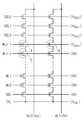
메모리 셀 어레이(100)는 데이터 정보를 저장하기 위한 영역으로, 행들(또는, 워드 라인들)과 열들(또는, 비트 라인들)로 배열된 메모리 셀들을 포함할 것이다. 메모리 셀들 각각은 1-비트 데이터 또는 N-비트 데이터(N은 2 또는 그 보다 큰 정수)를 저장할 것이다. 메모리 셀들은 복수의 메모리 블록들(또는, 섹터들)을 구성할 것이다. 하나의 메모리 블록에 속하는 메모리 셀들의 예시적인 배열이 도 2에 도시되어 있다. 도 2에 도시된 바와 같이, 메모리 셀들은 복수의 스트링들(또는, 낸드 스트링이라 불림)(101)을 구성하도록 배열될 것이다. 스트링들(101)은 대응하는 비트 라인들(BL0∼BLm-1)에 각각 연결될 것이다.The
비트 라인(BL0)에 대응하는 스트링(101)은 스트링 선택 트랜지스터들(SST0, SST1, SST2), 공통 소오스 라인(CSL)에 전기적으로 연결된 접지 선택 트랜지스터(GST), 그리고 선택 트랜지스터들(SST2, GST) 사이에 직렬 연결된 복수의 메모리 셀들(M0∼Mn)을 포함할 것이다. 스트링 선택 트랜지스터들(SST0, SST1, SST2)은 대응하는 스트링 선택 라인들(SSL0, SSL1, SSL2)에 각각 전기적으로 연결되고, 접지 선택 트랜지스터(GST)는 접지 선택 라인(GSL)에 전기적으로 연결되며, 메모리 셀들(M0∼Mn)은 대응하는 워드 라인들(WL0∼WLn)에 각각 전기적으로 연결된다. 나머지 비트 라인들(BL1BLn)에 각각 대응하는 스트링들(101)은 비트 라인(BL0)에 대응하는 스트링(101)과 동일하게 구성되며, 그것에 대한 설명은 그러므로 생략될 것이다. 여기서, 각 스트링에 속하는 스트링 선택 트랜지스터들의 수는 다양하게 변경될 수 있음은 이 분야의 통상적인 지식을 습득한 자들에게 자명하다. 예를 들면, 각 스트링은 하나 또는 그 보다 많은 스트링 선택 트랜지스터들을 포함하도록 구성될 수 있다.The string 101 corresponding to the bit line BL0 includes string selection transistors SST0, SST1 and SST2, a ground selection transistor GST electrically connected to the common source line CSL, and selection transistors SST2 and GST And a plurality of memory cells M0 to Mn connected in series between the memory cells M0 to Mn. The string selection transistors SST0, SST1 and SST2 are electrically connected to the corresponding string selection lines SSL0, SSL1 and SSL2, respectively, and the ground selection transistor GST is electrically connected to the ground selection line GSL , And the memory cells M0 to Mn are electrically connected to the corresponding word lines WL0 to WLn, respectively. The strings 101 corresponding to the remaining bit lines BL1BLn are each configured the same as the string 101 corresponding to the bit line BL0 and the description thereof will be omitted. It will be apparent to those skilled in the art that the number of string select transistors belonging to each string can vary widely. For example, each string may be configured to include one or more string selection transistors.
본 발명의 예시적인 실시예에 있어서, 메모리 셀들은 전하 저장층을 갖는 다양한 셀 구조들 중 하나를 이용하여 구현될 수 있다. 전하 저장층을 갖는 셀 구조는 플로팅 게이트를 이용하는 플로팅 게이트 타입 플래시 구조, 전하 트랩층을 이용하는 전하 트랩 플래시 구조, 어레이들이 다층으로 적층되는 스택 플래시 구조, 소오스-드레인이 없는 플래시 구조, 핀-타입 플래시 구조, 등을 포함할 것이다.In an exemplary embodiment of the present invention, the memory cells may be implemented using one of various cell structures having a charge storage layer. The cell structure having the charge storage layer may be a floating gate type flash structure using a floating gate, a charge trap flash structure using a charge trap layer, a stack flash structure in which arrays are stacked in multiple layers, a flash structure without a source- Structure, and the like.
다시 도 1을 참조하면, 행 디코더 회로(200)는 제어 로직(500)의 제어에 응답하여 동작하며, 행 어드레스(미도시됨)에 따라 메모리 셀 어레이(100)의 행들을 선택 및 구동할 것이다. 열 디코더 회로(300)는 제어 로직(500)의 제어에 응답하여 동작하며, 열 어드레스(미도시됨)에 따라 메모리 셀 어레이(100)의 열들을 선택할 것이다. 읽기 및 쓰기 블록(400)은 제어 로직(500)의 제어에 응답하여 동작하며, 동작 모드에 따라 메모리 셀 어레이(100)로부터 데이터를 읽거나 그것으로 데이터 를 쓰도록 구성될 것이다. 메모리 셀 어레이(100)에 저장될 데이터는 읽기 및 쓰기 블록(400)에 임시 저장될 것이다. 제어 로직(500)은 불 휘발성 메모리 장치(1000)의 전반적인 동작을 제어하도록 구성될 것이다. 전압 발생 회로(600)는 제어 로직(500)의 제어에 응답하여 동작하며, 동작 모드에 따라 필요한 전압들(예를 들면, 패스 전압, 소거 전압, 읽기 전압, 등)을 발생할 것이다.Referring again to Figure 1, the
이후 설명되는 바와 같이, 본 발명의 전압 발생 회로(600)는 일반적인 플래시 메모리 장치의 프로그램 동작시 필요한 프로그램 전압을 발생하지 않는다. 다시 말해서, 본 발명의 불 휘발성 메모리 장치(1000)는 프로그램 전압을 사용하지 않고 메모리 셀을 프로그램할 수 있는 새로운 프로그램 스킴을 제공할 것이다. 새로운 프로그램 스킴에 따르면, 프로그램 동작시 F-N 터널링 스킴 대신에 게이트 유기 드레인 누설(Gate-Induced Drain Leakage)(이하, 'GIDL'로 표기됨)로 인해 생성되는 열-전자(hot-electron)을 이용하여 프로그램 동작을 수행하는 것이 가능하다. 이는 이후 상세히 설명될 것이다.As will be described later, the voltage generating
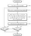
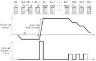
도 3은 본 발명의 예시적인 실시예들에 따른 불 휘발성 메모리 장치의 프로그램 동작을 설명하기 위한 흐름도이고, 도 4는 본 발명의 예시적인 실시예들에 따른 불 휘발성 메모리 장치의 프로그램 동작시 바이어스 조건을 보여주는 도면이다. 도 5는 본 발명의 프로그램 방법에 따른 전자 주입 메카니즘을 개략적으로 설명하기 위한 도면이다.FIG. 3 is a flowchart for explaining a program operation of a nonvolatile memory device according to exemplary embodiments of the present invention, and FIG. 4 is a flowchart illustrating a program operation of a nonvolatile memory device according to exemplary embodiments of the present invention, Fig. 5 is a view for schematically explaining an electron injection mechanism according to the programming method of the present invention.
이하, 본 발명의 예시적인 실시예들에 따른 불 휘발성 메모리 장치의 프로그램 방법이 참조 도면들에 의거하여 상세히 설명될 것이다. 설명에 앞서, 잘 알려진 바와 같이, 프로그램 동작은 복수의 프로그램 루프들을 통해 수행될 것이다. 각 프로그램 루프는 프로그램 실행 구간과 검증 읽기 구간을 포함할 것이다. 프로그램 실행 구간은 선택된 메모리 셀들이 실질적으로 프로그램 되는 구간을 나타내며, 검증 읽기 구간은 선택된 메모리 셀들이 정상적으로 프로그램되었는 지의 여부를 판별하는 구간을 나타낸다. 프로그램 루프들은 선택된 메모리 셀들이 모두 정상적으로 프로그램될 때까지 정해진 횟수 내에서 반복적으로 수행될 것이다.Hereinafter, a programming method of a nonvolatile memory device according to exemplary embodiments of the present invention will be described in detail with reference to the drawings. Prior to the description, as is well known, the program operation will be performed through a plurality of program loops. Each program loop will contain a program execution interval and a verification read interval. The program execution period represents a period in which the selected memory cells are substantially programmed, and the verify read period represents a period for determining whether or not the selected memory cells are normally programmed. Program loops will be iteratively performed within a predetermined number of times until all of the selected memory cells are normally programmed.
먼저, 단계 S100에서, 메모리 셀 어레이(100)에 프로그램될 데이터는 제어 로직(500)의 제어에 따라 열 디코더 회로(300)를 통해 읽기 및 쓰기 블록(400)에 로드될 것이다. 단계 S110에서는, 로드된 데이터에 따라 비트 라인들(BL0∼BLm-1)이 전원전압(VCC) 또는 접지 전압으로 설정되고, 스트링들(101)의 채널들이 프리챠지될 것이다. 설명의 편의상, 워드 라인(WLn-1)이 선택된다고 그리고 선택된 워드 라인(WLn-1)의 메모리 셀(A)이 프로그램될 메모리 셀이고 선택된 워드 라인(WLn-1)의 메모리 셀(B)이 프로그램 금지될 메모리 셀이라 가정한다.First, at step S100, the data to be programmed into the
이러한 가정에 따르면, 도 4에 도시된 바와 같이, 프로그램될 메모리 셀(A)에 대응하는 비트 라인(BL0)은 읽기 및 쓰기 블록(400)을 통해 전원 전압(VCC)으로 설정되는 반면에, 프로그램 금지될 메모리 셀(B)에 대응하는 비트 라인(BL1)은 읽기 및 쓰기 블록(400)을 통해 접지 전압으로 설정될 것이다. 그 다음에, 스트링 선택 라인들(SSL0, SSL1, SSL2)은 제어 로직(500)의 제어에 따라 행 디코더 회로(200)를 통해 대응하는 선택 라인 전압들(VSSL0, VSSL1, VSSL2)로 각각 구동되고, 접지 선택 라인(GSL)은 접지 전압으로 구동될 것이다. 이는 각 스트링(101)이 설정된 전압으로 프리챠지됨을 의미한다. 예를 들면, 비트 라인(BL0)에 대응하는 스트링의 채널은 (VSSL0-Vth)(Vth는 SST0의 문턱 전압)의 전압으로 프리챠지되고, 비트 라인(BL1)에 대응하는 스트링의 채널은 0V의 전압으로 프리챠지될 것이다. 비트 라인(BL0)에 대응하는 스트링의 채널이 (VSSL0-Vth)의 전압으로 프리챠지됨에 따라, 비트 라인(BL0)에 대응하는 스트링의 스트링 선택 트랜지스터(SST0)는 셧-오프될 것이다(턴-오프될 것이다).According to this assumption, the bit line BL0 corresponding to the memory cell A to be programmed is set to the power supply voltage VCC through the read and write
여기서, 선택 라인 전압들(VSSL0, VSSL1, VSSL2)은 서로 다르게 설정될 것이다. 예를 들면, 선택 라인 전압(VSSL0)은 선택 라인 전압(VSSL1)보다 낮고, 선택 라인 전압(VSSL1)은 선택 라인 전압(VSSL2)보다 낮다. 즉, 선택 라인 전압들(VSSL0, VSSL1, VSSL2)은 이 순서로 단계적으로 증가될 것이다. 즉, 워드 라인(또는, 최상위 워드 라인)에 인접한 선택 트랜지스터(예를 들면, SST2)의 선택 라인 전압이 비트 라인에 인접한 선택 트랜지스터(예를 들면, SSL0)의 선택 라인 전압보다 높다. 이는 워드 라인과 선택 라인 사이의 전압차를 감소시킴으로써 이후 설명될 GIDL로 인한 열-전자의 생성을 방지하기 위함이다.Here, the selection line voltages VSSL0 , VSSL1 , and VSSL2 will be set to be different from each other. For example, the select line voltage (VSSL0) is lower than the select line voltage (VSSL1), the select line voltage (VSSL1) is lower than the select line voltage (VSSL2). That is, the selection line voltages VSSL0 , VSSL1 , and VSSL2 will be incrementally increased in this order. That is, the select line voltage of the select transistor (for example, SST2) adjacent to the word line (or the most significant word line) is higher than the select line voltage of the select transistor (for example, SSL0) adjacent to the bit line. This is to prevent the generation of thermo-electrons due to GIDL, which will be described later, by reducing the voltage difference between the word line and the select line.
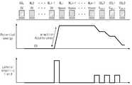
다음 단계(S120)에서는, 선택된 워드 라인(WLn-1)과 선택된 워드 라인(WLn-1)보다 위에 위치하는 워드 라인들(또는,선택된 워드 라인(WLn-1)과 스트링 선택 라인(SSL2) 사이에 위치한 워드 라인들)은 제어 로직(500)의 제어에 따라 행 디코더 회로(200)를 통해 패스 전압(Vpass)으로 각각 구동될 것이다. 이와 동시에, 도 4에 도시된 바와 같이, 선택된 워드 라인(WLn-1)보다 아래에 위치한 워드 라인들(WLn-2∼WL0)(또는, 선택된 워드 라인(WLn-1)과 접지 선택 라인(GSL) 사이에 위치한 워드 라인들)에는 접지 전압(0V)이 공급될 것이다. 워드 라인(WLn-2)이 선택되는 경우, 선택된 워드 라인과 선택된 워드 라인보다 위에 위치하는 워드 라인(들) 즉, 워드 라인들(WLn-2, WLn-1)은 모두 패스 전압(Vpass)으로 구동될 것이다. 이러한 바이어스 조건에 따르면, 비트 라인(BL0)에 대응하는 스트링의 채널은 스트링 선택 트랜지스터(SST0)가 턴-오프되어 있기 때문에 패스 전압(Vpass)의 공급에 따라 셀프 부스팅되는 반면에, 비트 라인(BL1)에 대응하는 스트링의 채널은 스트링 선택 트랜지스터들(SST0, SST1, SST2)이 턴-온되어 있기 때문에 패스 전압(Vpass)의 공급에 관계없이 접지 전압으로 유지될 것이다. 비트 라인(BL0)에 대응하는 스트링의 채널이 패스 전압(Vpass)의 공급에 따라 셀프 부스팅됨에 따라, 인접한 메모리 셀(C)의 드레인에서 GIDL로 인해 전자들이 생성되며, 그렇게 생성된 전자들은 메모리 셀(A)의 전하 저장층으로 주입될 것이다. 즉, 메모리 셀(A)이 프로그램될 것이다. 좀 더 구체적인 설명은 도 5를 참조하여 행해질 것이다.In the next step S120, the selected word line WLn-1 and the word lines WLn-1 located above the selected word line WLn-1 (or between the selected word line WLn-1 and the string selection line SSL2) Will be driven to the pass voltage Vpass through the
도 5를 참조하면, 메모리 셀(A)의 채널 전압은 선택된 워드 라인(WLn-1)에 패스 전압(Vpass)이 인가될 때 프리챠지된 전압에서 소정의 전압(예를 들면, 6V∼10V)으로 부스팅될 것이다. 이때, 인접한 워드 라인(WLn-2)에 접지 전압(0V)이 인가되기 때문에, 메모리 셀(C)의 채널 전압은 기판 전압으로 유지될 것이다. 이러한 바이어스 조건에 따르면, 부스팅된 채널 전압의 n+ 영역에서 기판으로 전계(E1) 가 가해지고, 부스팅된 채널 전압의 n+ 영역에서 워드 라인(WLn-2)으로 전계(E2)가 가해질 것이다. 그러한 전계들(E1, E2)에 의해서 전자-홀 쌍들(Electron-Hole Pairs)이 생성되며, 생성된 전자-홀 쌍들 중 홀들은 기판으로 빠져나가고, 생성된 전자-홀 쌍들 중 전자들은 n+ 영역으로 빠져나갈 것이다. 이러한 현상은, 이 분야에 잘 알려진 바와 같이, GIDL(Gate-Induced Drain Leakage)이라 불린다. GIDL으로 인해 생성된 전자들은 워드 라인들(WLn-1, WLn-2) 사이의 전압차로 인해 생기는 전계에 의해서 가속되며, 가속된 전자들(즉, 열-전자들)은 메모리 셀(A)의 전하 저장층으로 주입될 것이다. 이는 메모리 셀(A)이 프로그램됨을 의미한다. 이에 반해서, 비트 라인(BL1)에 대응하는 스트링의 메모리 셀(B)의 경우, 채널 전압이 0V으로 유지되기 때문에, 앞서 설명된 GIDL 현상은 유발되지 않을 것이다. 그러한 까닭에, 비트 라인(BL1)에 대응하는 스트링의 메모리 셀(B)은 프로그램 금지될 것이다.5, the channel voltage of the memory cell A is set to a predetermined voltage (for example, 6 V to 10 V) at a precharge voltage when the pass voltage Vpass is applied to the selected word line WLn- . At this time, since the ground voltage (0 V) is applied to the adjacent word line WLn-2, the channel voltage of the memory cell C will be maintained at the substrate voltage. According to this bias condition, the electric field E1 is applied to the substrate in the n + region of the boosted channel voltage and the electric field E2 is applied to the word line WLn-2 in the n + region of the boosted channel voltage. Electrone-hole pairs are generated by such electric fields E1 and E2, holes in the generated electron-hole pairs pass to the substrate, and electrons in the generated electron-hole pairs are recombined into the n + region I will escape. This phenomenon is referred to as GIDL (Gate-Induced Drain Leakage), as is well known in the art. Electrons generated due to GIDL are accelerated by an electric field generated due to a voltage difference between the word lines WLn-1 and WLn-2, and accelerated electrons (i.e., heat-electrons) Charge storage layer. This means that the memory cell A is programmed. On the other hand, in the case of the memory cell B of the string corresponding to the bit line BL1, since the channel voltage is maintained at 0V, the GIDL phenomenon described above will not be caused. Hence, the memory cell B of the string corresponding to the bit line BL1 will be program inhibited.
본 발명의 불 휘발성 메모리 장치에 있어서, 선택된 워드 라인(WLn-1)과 스트링 선택 라인 사이의 전압차가 클 경우, 앞서 설명된 GIDL로 인해 열-전자가 메모리 셀(A)의 드레인 측에서 생성될 것이다. 이를 방지하기 위해서, 스트링 선택 라인들(SSL2, SST1, SST0)에 인가되는 선택 라인 전압들(VSSL2, VSSL1, VSSL0)은 단계적으로 감소되도록 설정될 것이다. 선택 라인 전압들(VSSL2, VSSL1, VSSL0)은 단계적으로 감소되기 때문에, 최상위 워드 라인(WLn-1)과 스트링 선택 라인(SSL2) 사이의 전압차로 인한 열-전자의 생성은 방지될 것이다.In the nonvolatile memory device of the present invention, when the voltage difference between the selected word line WLn-1 and the string selection line is large, due to the GIDL described above, the column-electron is generated at the drain side of the memory cell A will be. In order to prevent this, the selection line voltages VSSL2 , VSSL1 , VSSL0 applied to the string selection lines SSL2, SST1,SST0 will be set to decrease stepwise. Since the select line voltages VSSL2 , VSSL1 and VSSL0 are stepped down, the generation of thermo-electrons due to the voltage difference between the most significant word line WLn-1 and the string select line SSL2 will be prevented .
다시 도 3을 참조하면, S130 단계에서는, 선택된 워드 라인(WLn-1)의 메모리 셀들(A)로부터 데이터를 읽기 위한 검증 읽기 동작이 수행될 것이다. 검증 읽기 동작이 수행되기 이전에 워드 라인들 및 비트 라인들에 인가된 전압들을 방전시키기 위한 리커버리 동작이 수행될 것이다. 검증 읽기 동작은, 앞서 설명된 바와 같이, 제어 로직(500)의 제어에 따라 읽기 및 쓰기 블록(400)을 통해 수행될 것이다. 검증 읽기 동작의 바이어스 조건은 일반적인 플래시 메모리 장치와 동일하며, 그것에 대한 설명은 그러므로 생략될 것이다. 다음 단계(S140)에서는, 제어 로직(500)은 검증 읽기 동작의 결과에 따라 읽혀진 데이터에 의거하여, 선택된 메모리 셀들이 정상적으로 수행되었는 지의 여부를 판별할 것이다. 즉, 제어 로직(500)은 검증 읽기 동작의 결과에 따라 읽혀진 데이터에 의거하여, 프로그램 동작이 패스되었는 지의 여부를 판별할 것이다. 판별 결과가 프로그램 패스를 나타내면, 프로그램 절차는 종료될 것이다. 반면에, 판별 결과가 프로그램 페일을 나타내면, 절차는 S150 단계로 진행하며, S150 단계에서는 현재의 프로그램 루프가 최대 프로그램 루프에 도달하였는 지의 여부가 제어 로직(500)에 의해서 판별될 것이다. 현재의 프로그램 루프가 최대 프로그램 루프에 도달한 것으로 판별되면, 프로그램 절차는 프로그램 페일로서 종료될 것이다. 현재의 프로그램 루프가 최대 프로그램 루프에 도달하지 않은 것으로 판별되면, 절차는 S110 단계로 진행할 것이다. 이후, 다음의 프로그램 루프가 앞서 설명될 것과 동일한 방식으로 수행될 것이다.Referring again to FIG. 3, in step S130, a verify read operation for reading data from the memory cells A of the selected word line WLn-1 will be performed. A recovery operation to discharge the voltages applied to the word lines and bit lines before the verify read operation is performed will be performed. The verify read operation will be performed through the read and write
상술한 바와 같이, 본 발명에 따른 불 휘발성 메모리 장치(1000)는 낸드 플래시 메모리 장치임에도 불구하고 F-N 터널링 방식 대신 열-전자 주입 방식을 통해 메모리 셀들을 프로그램할 것이다. 다시 말해서, 본 발명에 따른 불 휘발성 메모리 장치(1000)는 F-N 터널링 방식 대신에 GIDL로 인해 생성된 전자들을 전하 저장층에 주입하는 방식을 이용하여 메모리 셀들을 프로그램할 것이다. 본 발명의 불 휘발성 메모리 장치는 프로그램 전압과 패스 전압과 같은 고전압들을 필요로 하는 전압 방식 대신 패스 전압만을 필요로 하는 전계 방식을 채용할 것이다. 불 휘발성 메모리 장치의 스케일-다운시 생기는 문제점들은 그러한 전계 방식을 채용함으로써 최소화될 것이다. 예를 들면, F-N 터널링 방식을 통해 프로그램 동작을 수행하는 불 휘발성 메모리 장치의 경우, 프로그램 전압, 채널 부스팅 전압, 인접한 스트링들 사이에 형성되는 트렌치의 깊이, 그리고 워드 라인들 사이의 브레이크다운은 불 휘발성 메모리 장치의 스케일-다운에 무관하게 일정하게 유지되어야 한다. 즉, F-N 터널링을 위한 바이어스 조건을 변경하는 것이 불가능하기 때문에, 불 휘발성 메모리 장치의 스케일-다운시 그러한 항목들을 줄이는 것 역시 불가능하다. 이에 반해서, GIDL을 통해 생성된 열-전자를 이용하여 프로그램 동작을 수행하는 불 휘발성 메모리 장치의 경우, 채널 부스팅 전압, 프로그램/패스 전압, 인접한 스트링들 사이에 형성되는 트렌치의 깊이, 그리고 워드 라인들 사이의 브레이크다운은 불 휘발성 메모리 장치의 스케일-다운에 비례해서 단계적으로 감소될 수 있다. 즉, 전계의 세기가 절연막의 두께에 반비례하고 전압에 비례하며, 스케일-다운시 절연막의 두께가 감소할 것이다. 이는 절연막 두께의 감소에 비례하여 전압을 감소시키더라도 동일한 전계의 세기를 얻는 것이 가능함을 의미한다. 따라서, 불 휘발성 메모리 장치의 스케일-다운시 그러한 항목들을 줄이는 것이 가능하다. 결과적으로, 본 발명에 따른 프로그램 방식을 채용함으로써 스케일다운으로 인한 쟁점없이 불 휘발성 메모리 장치를 스케일-다운시키는 것이 가능하다.As described above, the
도 6은 본 발명의 예시적인 실시예들에 따른 불 휘발성 메모리 장치의 프로그램 동작시 채널 전위 및 수평 전계의 관계를 개략적으로 보여주는 도면이다.6 is a schematic view showing a relationship between a channel potential and a horizontal electric field in a program operation of a nonvolatile memory device according to exemplary embodiments of the present invention.
워드 라인(WLi)이 선택된 경우 프로그램 동작의 바이어스 조건이 도 6에 도시되어 있다. 앞서 설명된 바와 같이, 선택된 워드 라인(WLi)과 선택된 워드 라인(WLi)보다 위에 위치한 워드 라인들(WLi+1∼WLn-1) 즉, 워드 라인들(WLi∼WLn-1)은 패스 전압(Vpass)으로 구동되고, 나머지 워드 라인들(WL0∼WLi-1)은 접지 전압(0V)으로 구동된다. 이와 동시에, 선택 라인들(SSL0, SSL1, SSL2)은 대응하는 선택 라인 전압들(VSSL0, VSSL1, VSSL2)로 각각 구동된다. 선택 라인 전압들(VSSL0, VSSL1, VSSL2)은 워드 라인 방향으로 단계적으로 증가되도록 설정될 것이다.The bias condition of the program operation when the word line WLi is selected is shown in Fig. As described above, the word lines WLi + 1 to WLn-1, that is, the word lines WLi to WLn-1 located above the selected word line WLi and the selected word line WLi, Vpass, and the remaining word lines WL0 to WLi-1 are driven to the ground voltage (0 V). At the same time, the selection lines SSL0, SSL1 and SSL2 are driven respectively with the corresponding selection line voltages VSSL0 , VSSL1 and VSSL2 . The selection line voltages VSSL0 , VSSL1 , and VSSL2 will be set to increase stepwise in the word line direction.
상술한 바이어스 조건에 따르면, 워드 라인들(WLi∼WLn-1)에 연결된 메모리 셀들의 채널들은 패스 전압(Vpass)이 인가될 때 부스팅되는 반면에, 나머지 워드 라인들(WL0∼WLi-1)에 연결된 메모리 셀들의 채널들은 기판 전압으로 유지될 것이다. 결과적으로, 워드 라인(WLi)에 연결된 메모리 셀과 워드 라인(WLi-1)에 연결된 메모리 셀의 채널 전위들의 차에 대응하는 전계(즉, 수평 전계)가 인접 워드 라인들(WLi, WLi-1) 사이에 형성될 것이다. 그러한 전계에 의해서 전자들이 가속되고, 가속된 전자들(즉, 열-전자)이 워드 라인(WLi)에 연결된 메모리 셀의 전하 저장층으로 주입될 것이다. 이에 반해서, 선택된 워드 라인(WLi)과 스트링 선택 라인(SSL2) 사이에 위치한 워드 라인들의 경우, 인접한 워드 라인들 사이에 전위가 없기 때문에, 수평 전계가 형성되지 않을 것이다. 선택 라인 전압들(VSSL2, VSSL1, VSSL0) (또는, 채널 전위)이 단계적으로 감소하기 때문에, 도 6에 도시된 바와 같이, 수평 전계는 GIDL을 유발하지 않을 정도로 형성될 것이다.According to the above-described bias condition, the channels of the memory cells connected to the word lines WLi to WLn-1 are boosted when the pass voltage Vpass is applied, while the other word lines WL0 to WLi- The channels of the connected memory cells will be maintained at the substrate voltage. As a result, an electric field (i.e., a horizontal electric field) corresponding to the difference between the channel potentials of the memory cells connected to the word line WLi and the memory cells connected to the word line WLi-1 is applied to the adjacent word lines WLi and WLi-1 . The electrons are accelerated by such an electric field and accelerated electrons (i.e., heat-electrons) will be injected into the charge storage layer of the memory cell connected to the word line WLi. On the other hand, in the case of the word lines located between the selected word line WLi and the string selection line SSL2, a horizontal electric field will not be formed because there is no potential between adjacent word lines. Since the select line voltages VSSL2 , VSSL1 , VSSL0 (or channel potential) decrease stepwise, the horizontal electric field will be formed to such an extent as not to cause GIDL, as shown in FIG.
도 7은 본 발명의 다른 예시적인 실시예들에 따른 프로그램 바이어스 조건을 보여주는 도면이다.7 is a diagram showing program bias conditions according to other exemplary embodiments of the present invention.
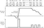
도 7을 참조하면, 선택된 워드 라인(WLi)은 패스 전압(Vpass)보다 높은 전압(Vhipass)으로 구동되는 반면에, 나머지 워드 라인들(WL0∼WLi-1, WLi+1∼WLn-1) 및 스트링 선택 라인들(SSL0, SSL1, SSL2)은 도 6에서 설명된 것과 동일하게 바이어스될 것이다. 이러한 바이어스 조건에 따르면, 워드 라인들(WLi-1, WLi) 사이에 형성되는 수평 전계가 도 6에서 설명된 것과 비교하여 볼 때 상대적으로 커질 것이다. 그렇게 형성된 수평 전계에 의해서 전자들이 가속되고, 가속된 전자들은 선택된 메모리 셀의 전하 저장층에 주입될 것이다. 이러한 점을 제외하면, 도 7에 도시된 프로그램 동작의 바이어스 조건은 도 6에 도시된 것과 실질적으로 동일하며, 그것에 대한 설명은 그러므로 생략될 것이다.7, the selected word line WLi is driven with a voltage Vhipass higher than the pass voltage Vpass while the other word lines WL0 to WLi-1, WLi + 1 to WLn-1 and The string selection lines SSL0, SSL1, SSL2 will be biased as described in FIG. According to this bias condition, the horizontal electric field formed between the word lines WLi-1, WLi will be relatively large as compared with that described in Fig. The electrons are accelerated by the horizontal electric field thus formed, and the accelerated electrons will be injected into the charge storage layer of the selected memory cell. Except for this point, the bias condition of the program operation shown in Fig. 7 is substantially the same as that shown in Fig. 6, and a description thereof will therefore be omitted.
도 8은 본 발명의 다른 예시적인 실시예들에 따른 프로그램 바이어스 조건을 보여주는 도면이다.8 is a diagram showing program bias conditions according to other exemplary embodiments of the present invention.
도 8을 참조하면, 선택된 워드 라인(WLi)과 접지 선택 라인(GSL) 사이에 위치한 워드 라인들(WL0∼WLi-1)은 접지 전압보다 높은 전압(Vlow)으로 구동되는 반면에, 나머지 워드 라인들(WLi∼WLn-1) 및 스트링 선택 라인들(SSL0, SSL1, SSL2) 은 도 6에서 설명된 것과 동일하게 바이어스될 것이다. 이러한 바이어스 조건에 따르면, 워드 라인들(WLi-1, WLi) 사이에 형성되는 수평 전계가 도 6의 바이어스 조건에 따른 생성된 것과 비교하여 볼 때 상대적으로 작아질 것이다. 이러한 점을 제외하면, 도 8에 도시된 프로그램 동작의 바이어스 조건은 도 6에 도시된 것과 실질적으로 동일하며, 그것에 대한 설명은 그러므로 생략될 것이다.8, the word lines WL0 to WLi-1 located between the selected word line WLi and the ground selection line GSL are driven at a voltage (Vlow) higher than the ground voltage, while the remaining word lines WL1 to WLn-1 and string selection lines SSL0, SSL1 and SSL2 will be biased as described in Fig. According to this bias condition, the horizontal electric field formed between the word lines WLi-1 and WLi will be relatively small as compared with that generated according to the bias condition of FIG. Except for this point, the bias condition of the program operation shown in Fig. 8 is substantially the same as that shown in Fig. 6, and a description thereof will therefore be omitted.
도 9는 본 발명의 다른 예시적인 실시예들에 따른 프로그램 바이어스 조건을 보여주는 도면이다.9 is a diagram showing program bias conditions according to other exemplary embodiments of the present invention.
도 9를 참조하면, 선택된 워드 라인(WLi)의 바로 아래에 위치한 워드 라인(WLi-1)은 접지 전압 대신 음의 전압(예를 들면, -3V)으로 구동되고, 나머지 워드 라인들(WL0∼WLi-2, WLi∼WLn-1) 및 스트링 선택 라인들(SSL0, SSL1, SSL2)은 도 6에서 설명된 것과 동일하게 바이어스될 것이다. 이러한 바이어스 조건에 따르면, 워드 라인들(WLi-1, WLi) 사이에 형성되는 수평 전계가 도 6의 바이어스 조건에 따른 것보다 커질 것이다. 이러한 점을 제외하면, 도 9에 도시된 프로그램 동작의 바이어스 조건은 도 6에 도시된 것과 실질적으로 동일하며, 그것에 대한 설명은 그러므로 생략될 것이다.9, the word line WLi-1 located immediately below the selected word line WLi is driven with a negative voltage (for example, -3V) instead of the ground voltage, and the remaining word lines WL0- WLi-2, WLi-WLn-1 and string selection lines SSL0, SSL1, SSL2 will be biased as described in FIG. According to this bias condition, the horizontal electric field formed between the word lines WLi-1 and WLi will become larger than that according to the bias condition of FIG. Except for this point, the bias condition of the program operation shown in Fig. 9 is substantially the same as that shown in Fig. 6, and a description thereof will therefore be omitted.
도 10은 본 발명의 다른 예시적인 실시예들에 따른 프로그램 바이어스 조건을 보여주는 도면이다.10 is a diagram showing program bias conditions according to other exemplary embodiments of the present invention.
도 10을 참조하면, 선택된 워드 라인(WLi)과 접지 선택 라인(GSL) 사이에 위치한 워드 라인들(WL0∼WLi-1)은 접지 전압 대신 음의 전압(예를 들면, -3V)으로 구동되며, 나머지 워드 라인들(WLi∼WLn-1) 및 스트링 선택 라인들(SSL0, SSL1, SSL2)은 도 6에서 설명된 것과 동일하게 바이어스될 것이다. 이러한 바이어스 조건에 따르면, 워드 라인들(WLi-1, WLi) 사이에 형성되는 수평 전계가 도 6의 바이어스 조건에 따른 것보다 커질 것이다. 이러한 점을 제외하면, 도 10에 도시된 프로그램 동작의 바이어스 조건은 도 6에 도시된 것과 실질적으로 동일하며, 그것에 대한 설명은 그러므로 생략될 것이다.10, the word lines WL0 to WLi-1 located between the selected word line WLi and the ground selection line GSL are driven with a negative voltage (for example, -3 V) instead of the ground voltage , The remaining word lines WLi to WLn-1 and the string selection lines SSL0, SSL1 and SSL2 will be biased as described in Fig. According to this bias condition, the horizontal electric field formed between the word lines WLi-1 and WLi will become larger than that according to the bias condition of FIG. Except for this point, the bias condition of the program operation shown in Fig. 10 is substantially the same as that shown in Fig. 6, and the description thereof will therefore be omitted.
도 9 및 도 10에서 설명된 바이어스 조건에 따르면, 워드 라인(들)로 음의 전압이 공급될 것이다. 이러한 경우, 행 디코더 회로(200)는 음의 전압을 스위치할 수 있는 고전압 전달 회로를 구비하여야 할 것이다.According to the bias conditions described in Figs. 9 and 10, a negative voltage will be supplied to the word line (s). In such a case, the
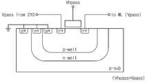
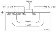
고전압 전달 회로를 포함한 행 디코더 회로를 개략적으로 보여주는 도 11을 참조하면, 행 디코더 회로(200)는 디코딩 및 구동 블록(210)과 고전압 전달 회로(220)를 포함할 것이다. 디코딩 및 구동 블록(210)은 고전압 전달 회로(220)를 통해 선택 라인들(SSL0, SSL1, SSL2, GSL) 및 워드 라인들(WL0∼WLn-1)을 구동할 것이다. 고전압 전달 회로(220)는 복수의 스위치 트랜지스터들(SWT)을 포함할 것이다. 스위치 트랜지스터들(SWT)은 음의 전압을 전달하기에 적합한 구조를 가질 것이다. 본 발명의 경우, 음의 전압을 전달하기 위해서, 스위치 트랜지스터들(SWT) 각각은 트리플-웰 구조(triple-well structure)를 갖도록 형성될 것이다. 즉, 도 12에 도시된 바와 같이, 스위치 트랜지스터들(SWT) 각각은 N-웰 내에 형성된 P-웰 내에 형성될 것이다. N-웰은 기판에 형성될 것이다. 즉, 각 스위치 트랜지스터(SWT)는 개별적으로 트리플-웰에 형성될 것이다. 음의 전압을 전달하지 않는 스위치 트랜지스터들 즉, 선택 라인들에 각각 대응하는 스위치 트랜지스터들이 기판에 직접 형성됨은 이 분야의 통상적인 지식을 습득한 자에게 자명하다. 고전압 전압 회로(220)의 트리플-웰은 메모리 셀 어레이(100)와 독립적으로 형성될 것이다.Referring to FIG. 11, which schematically illustrates a row decoder circuit including a high voltage transfer circuit, the
도 13은 고전압 전달 회로(220)를 통해 패스 전압이 공급될 때 웰 바이어스 조건을 보여주는 도면이고, 도 14는 고전압 전달 회로(220)를 통해 음의 전압이 공급될 때 웰 바이어스 조건을 보여주는 도면이다. 고전압 전달 회로(220)를 통해 패스 전압(Vpass)이 공급될 때, 도 13에 도시된 바와 같이, p-웰, n-웰, 그리고 기판은 접지 전압에 연결되고, 스위치 트랜지스터의 게이트에는 패스 전압(Vpass)보다 높은 고전압(Vhpass)이 공급될 것이다. 고전압 전달 회로(220)를 통해 음의 전압(예를 들면, -3V)이 공급될 때, 도 14에 도시된 바와 같이, n-웰과 기판은 접지 전압에 연결되고, p-웰은 음의 전압(예를 들면, -3V)에 연결되며, 스위치 트랜지스터의 게이트에는 패스 전압(Vpass)보다 높은 고전압(Vhpass)이 공급될 것이다.13 is a view showing a well bias condition when a pass voltage is supplied through the high
도 6 내지 도 10에서 설명된 것과 달리, 각 스트링은 하나의 스트링 선택 트랜지스터를 포함하도록 구성될 수 있다. 이러한 경우, 도 15에 도시된 바와 같이, 스트링 선택 라인(SSL0)과 인접 워드 라인(WLn-1) 사이의 간격은 GIDL로 인한 EHP의 생성을 방지하기에 충분하도록 넓게 설정될 것이다. 스트링 선택 라인(SSL0)과 인접 워드 라인(WLn-1) 사이의 간격이 넓기 때문에, 도 15에 도시된 바와 같이, 스트링 선택 라인(SSL0)과 인접 워드 라인(WLn-1) 사이에 형성되는 수평 전계의 세기는 일정하게 유지될 것이다. 다시 말해서, 워드 라인(WLn-1)과 스트링 선택 라인(SSL0) 사이의 채널 전위는 도 15에 도시된 바와 같이 점차적으로 감소될 것이다.6 to 10, each string may be configured to include one string selection transistor. In such a case, as shown in Fig. 15, the interval between the string selection line SSL0 and the adjacent word line WLn-1 will be set wide enough to prevent generation of EHP due to GIDL. 15, since the interval between the string selection line SSL0 and the adjacent word line WLn-1 is wide, the horizontal selection line SSL0 and the horizontal word line WLn-1 formed between the string selection line SSL0 and the adjacent word line WLn- The intensity of the electric field will be kept constant. In other words, the channel potential between the word line WLn-1 and the string selection line SSL0 will gradually decrease as shown in FIG.
예시적인 실시예에 있어서, 스트링 선택 트랜지스터들은 메모리 셀과 동일한 구조(동일한 형태 및 크기)를 갖도록 구성될 수 있다. 또는, 스트링 선택 트랜지스터들은 메모리 셀과 다른 구조(다른 형태 및 크기)를 갖도록 구성될 수도 있다. 선택 트랜지스터들 사이의 간격은 메모리 셀들 사이의 간격과 동일하게 또는 다르게 설정될 수 있다. 선택 트랜지스터와 메모리 셀 사이의 간격은 선택 트랜지스터들 사이의 간격과 다르게 또는 동일하게 설정될 수 있다. 스트링 선택 트랜지스터(SSL0)의 게이트 길이는 스트링 선택 트랜지스터들(SSL1, SSL2) 각각의 게이트 길이보다 크게 설정될 것이다. 또는, 스트링 선택 트랜지스터들(SSL0, SSL1, SSL2)의 게이트 길이들은 서로 동일하게 또는 서로 다르게 설정될 것이다.In an exemplary embodiment, the string selection transistors may be configured to have the same structure (same shape and size) as the memory cells. Alternatively, the string selection transistors may be configured to have a different structure (different shape and size) from the memory cell. The spacing between the select transistors may be set equal to or different from the spacing between the memory cells. The spacing between the select transistor and the memory cell may be set differently or the same as the spacing between the select transistors. The gate length of the string selection transistor SSL0 will be set larger than the gate length of each of the string selection transistors SSL1 and SSL2. Alternatively, the gate lengths of the string selection transistors SSL0, SSL1 and SSL2 may be set equal to each other or different from each other.
본 발명에 따른 불 휘발성 메모리 장치는 수직 어레이 구조를 갖도록 구성될 수 있다. 예시적인 수직 어레이 구조가 도 16에 도시되어 있다. 도 16에 도시된 바와 같이, 각 스트링은 일반적인 스트링 구조와 달리 비트 라인(BL)과 수직하게 형성되어 있다. 즉, 각 스트링은 기판에 수직하게 형성될 것이다. 수직 어레이 구조가 여기에 개시된 것에 국한되지 않음은 이 분야의 통상적인 지식을 습득한 자에게 자명하다. 도 16에 도시된 수직 어레이 구조를 갖는 불 휘발성 메모리 장치에도 앞서 언급된 프로그램 방법이 동일하게 적용되며, 설명의 편의상, 그것에 대한 설명은 그러므로 생략될 것이다.The nonvolatile memory device according to the present invention can be configured to have a vertical array structure. An exemplary vertical array structure is shown in Fig. As shown in FIG. 16, each string is formed perpendicular to the bit line BL, unlike a general string structure. That is, each string will be formed perpendicular to the substrate. It will be apparent to those skilled in the art that the vertical array structure is not limited to what is disclosed herein. The above-mentioned programming method is equally applied to the nonvolatile memory device having the vertical array structure shown in Fig. 16, and the description thereof will therefore be omitted for convenience of explanation.
예시적인 실시예에 있어서, 본 발명의 불 휘발성 메모리 장치는 공통 소오스 라인(CSL) 방향으로 워드 라인들이 순차적으로 선택되도록 구성될 것이다. 다시 말해서, 스트링 선택 라인(SSL0)에 바로 인접한 워드 라인(WLn-1)이 제일 먼저 선택 되고, 접지 선택 라인(GSL)에 바로 인접한 워드 라인(WL0)이 마지막으로 선택될 것이다. 이는 선택된 워드 라인과 접지 선택 라인(GSL) 사이에 위치한 메모리 셀들이 동일한 상태(즉, 소거 상태)로 유지된 상태에서 프로그램 동작이 수행됨을 의미한다. 이에 반해서, 본 발명의 불 휘발성 메모리 장치가 비트 라인 방향으로 워드 라인들이 순차적으로 선택되도록 구성될 수 있음은 이 분야의 통상적인 지식을 습득한 자에게 자명하다.In an exemplary embodiment, the nonvolatile memory device of the present invention will be configured such that the word lines are sequentially selected in the common source line (CSL) direction. In other words, the word line WLn-1 immediately adjacent to the string selection line SSL0 is selected first, and the word line WL0 immediately adjacent to the ground selection line GSL is finally selected. This means that the program operation is performed while the memory cells located between the selected word line and the ground selection line GSL are kept in the same state (i.e., the erase state). On the contrary, it is apparent to those skilled in the art that the nonvolatile memory device of the present invention can be configured so that the word lines are sequentially selected in the bit line direction.
앞서의 설명에 따르면, 선택된 워드 라인과 스트링 선택 라인 사이에 위치한 워드 라인들은 선택된 워드 라인과 동일한 전압(예를 들면, 패스 전압)으로 구동된다. 하지만, 선택된 워드 라인과 스트링 선택 라인 사이에 위치한 워드 라인들의 구동 전압이 여기에 개시된 것에 국한되지 않음은 이 분야의 통상적인 지식을 습득한 자에게 자명하다. 예를 들면, 선택된 워드 라인과 스트링 선택 라인 사이에 위치한 워드 라인들에 인가되는 전압들은 비트 라인 방향으로 단계적으로 감소되도록 설정될 수도 있다. 이러한 경우, 각 스트링에는 하나의 스트링 선택 트랜지스터가 구비될 수도 있다. 선택된 워드 라인과 스트링 선택 라인 사이에 위치한 워드 라인들에 인가되는 전압들이 비트 라인 방향으로 단계적으로 감소되기 때문에 최상위 워드 라인과 스트링 선택 라인 사이의 전압차는 GIDL의 생성을 방지하기에 충분히 작을 것이다.According to the foregoing description, the word lines located between the selected word line and the string selection line are driven with the same voltage (e.g., a pass voltage) as the selected word line. It will be apparent, however, to one of ordinary skill in the art that the driving voltage of the word lines located between the selected word line and the string selection line is not limited to that disclosed herein. For example, the voltages applied to the word lines located between the selected word line and the string selection line may be set to be gradually decreased in the bit line direction. In this case, one string selection transistor may be provided for each string. The voltage difference between the most significant word line and the string select line will be sufficiently small to prevent the generation of GIDL because the voltages applied to the word lines located between the selected word line and the string select line are stepped down in the bit line direction.
비록 도면에는 도시되지 않았지만, 본 발명에 따른 불 휘발성 메모리 장치는 스트링의 양측을 통해 선택된 메모리 셀을 프로그램하도록 구성될 수 있다. 다시 말해서, 앞서 설명된 것과 마찬가지로, 열-전자 주입 방식에 따라 선택된 메모리 셀의 소오스에서 생긴 열-전자가 전하 저장층에 주입될 것이다. 게다가, 열-전자 주입 방식에 따라 선택된 메모리 셀의 드레인에서 생긴 열-전자가 전하 저장층에 주입될 것이다. 결과적으로, 스트링에 속한 선택된 메모리 셀은 열-전자 주입 방식을 통해 2-비트 데이터로 프로그램될 것이다. 이를 위해서, 셀 어레이의 스트링들은 스트링 선택 라인 측에서 그리고 접지 선택 라인 측에서 프로그램될 데이터에 대응하는 전압이 각각 스트링의 채널로 전달되도록 구성될 것이다.Although not shown in the figure, a non-volatile memory device according to the present invention can be configured to program selected memory cells through both sides of the string. In other words, as previously described, the heat-electrons generated at the source of the selected memory cell in accordance with the thermal-electron injection scheme will be injected into the charge storage layer. In addition, heat-electrons generated in the drain of the selected memory cell in accordance with the thermal-electron injection method will be injected into the charge storage layer. As a result, the selected memory cell belonging to the string will be programmed with 2-bit data via a thermal-electron injection scheme. To this end, the strings of the cell array will be configured such that the voltages corresponding to the data to be programmed at the string select line side and at the ground select line side, respectively, are transferred to the channel of the string.
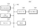
플래시 메모리 장치는 전력이 차단되어도 저장된 데이터를 유지할 수 있는 불 휘발성 메모리 장치이다. 셀룰러 폰, PDA 디지털 카메라, 포터블 게임 콘솔, 그리고 MP3P와 같은 모바일 장치들의 사용 증가에 따라, 플래시 메모리 장치는 데이터 스토리지 뿐만 아니라 코드 스토리지로서 보다 널리 사용된다. 플래시 메모리 장치는, 또한, HDTV, DVD, 라우터, 그리고 GPS와 같은 홈 어플리케이션에 사용될 수 있다. 본 발명에 따른 불 휘발성 메모리 장치를 포함한 컴퓨팅 시스템이 도 17에 개략적으로 도시되어 있다. 본 발명에 따른 컴퓨팅 시스템은 버스(2001)에 전기적으로 연결된 마이크로프로세서(2100), 사용자 인터페이스(2200), 베이스밴드 칩셋(baseband chipset)과 같은 모뎀(2300), 메모리 제어기(2400), 그리고 플래시 메모리 장치(2500)를 포함한다. 플래시 메모리 장치(2500)는 도 1에 도시된 것과 실질적으로 동일하게 구성될 것이다. 플래시 메모리 장치(2500)에는 마이크로프로세서(2100)에 의해서 처리된/처리될 N-비트 데이터(N은 1 또는 그 보다 큰 정수)가 메모리 제어기(2400)를 통해 저장될 것이다. 본 발명에 따른 컴퓨팅 시스템이 모바일 장치인 경우, 컴퓨팅 시스템의 동작 전압을 공급하기 위한 배터리(2600)가 추가 적으로 제공될 것이다. 비록 도면에는 도시되지 않았지만, 본 발명에 따른 컴퓨팅 시스템에는 응용 칩셋(application chipset), 카메라 이미지 프로세서(Camera Image Processor: CIS), 모바일 디램, 등이 더 제공될 수 있음은 이 분야의 통상적인 지식을 습득한 자들에게 자명하다. 메모리 제어기(2400)와 플래시 메모리 장치(2500)는, 예를 들면, 데이터를 저장하는 데 불 휘발성 메모리를 사용하는 SSD(Solid State Drive/Disk)를 구성할 수 있다. 예시적인 SSD가 미국특허공개번호 제2006-0152981호에 게재되어 있으며, 이 분야의 레퍼런스로 포함된다. 또는, 메모리 제어기(2400)와 플래시 메모리 장치(2500)는 데이터를 저장하는 데 불 휘발성 메모리를 메모리 카드를 구성할 수 있다.A flash memory device is a non-volatile memory device that can retain stored data even when power is turned off. With the increasing use of mobile devices such as cellular phones, PDA digital cameras, portable game consoles, and MP3Ps, flash memory devices are more widely used as code storage as well as data storage. Flash memory devices can also be used in home applications such as HDTV, DVD, routers, and GPS. A computing system including a non-volatile memory device according to the present invention is schematically illustrated in FIG. A computing system according to the present invention includes a
도 18은 본 발명의 다른 예시적인 실시예들에 따른 메모리 시스템을 보여주는 블록도이다.18 is a block diagram illustrating a memory system in accordance with another exemplary embodiment of the present invention.
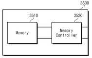
도 18에 도시된 메모리 시스템은 메모리(3510)와 메모리 제어기(3520)가 카드(3530)를 구성하도록 구현된다. 예를 들면, 카드(3530)는 플래시 메모리 카드와 같은 메모리 카드일 수 있다. 즉, 카드(3530)는 디지털, 카메라, 개인 컴퓨터 등과 같은 전자 장치를 사용하기 위한 어떤 산업 표준을 만족하는 카드일 수 있다. 메모리 제어기(3520)가 카드(3530)에 의해 또 다른 (예를 들면, 외부) 장치로부터 수신된 제어 신호들에 기초하여 메모리(3510)를 제어할 수 있다는 것이 이해될 것이다.The memory system shown in Fig. 18 is implemented such that the
도 19는 본 발명의 다른 예시적인 실시예들에 따른 메모리 시스템을 보여주는 블록도이다.19 is a block diagram illustrating a memory system in accordance with another exemplary embodiment of the present invention.
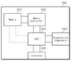
도 19에 도시된 시스템은 휴대용 장치(4000)를 나타낸다. 휴대용 장치(4000) 는 MP3 플레이어, 비디오 플레이어, 콤비네이션 비디오 및 오디오 플레이어 등일 수 있다. 도시된 바와 같이, 휴대용 장치(4000)는 메모리(3510) 및 메모리 제어기(3520)를 포함한다. 휴대용 장치(4000)는 또한 인코더 및 디코더(4610), 프리젠테이션 구성요소들(4620) 및 인터페이스(4630)를 포함할 수 있다.The system shown in Fig. 19 shows a
인코더 및 디코더(EDC)(4610)에 의해 처리된 데이터(비디오, 오디오, 등)는 메모리 제어기(3520)를 통해 메모리(3510)로 입력되고 메모리(3510)로부터 출력될 수 있다. 도 19에서 점선들에 의해 도시된 바와 같이, 데이터는 EDC(4610)로부터 메모리(3510)로 직접 입력되고 그리고/또는 메모리(3510)로부터 EDC(4610)로 직접 출력될 수 있다.Data (video, audio, etc.) processed by the encoder and decoder (EDC) 4610 may be input to and output from the
EDC(4610)는 메모리(3510)에 저장하기 위해 데이터를 인코딩할 수 있다. 예를 들면, EDC(4610)는 메모리(3510)에 저장하기 위해 오디오 데이터에 대해 MP3 인코딩을 수행할 수 있다. 다른 방법으로, EDC(4610)는 메모리(3510)에 저장하기 위해 비디오 데이터에 대해 MPEG 인코딩(예를 들면, MPEG2, MPEG4, 등)을 수행할 수 있다. 또한, EDC(4610)는 다른 데이터 포맷들에 따라 다른 타입들의 데이터를 인코딩하기 위한 복수의 인코더들을 포함할 수 있다. 예를 들면, EDC(4610)는 오디오 데이터를 위한 MP3 인코더 및 비디오 데이터를 위한 MPEG 인코더를 포함할 수 있다.
EDC(4610)는 메모리(3510)로부터의 출력을 디코딩할 수 있다. 예를 들면, EDC(4610)는 메모리(3510)로부터 출력된 오디오 데이터에 대해 MP3 디코딩을 수행할 수 있다. 다른 방법으로, EDC(4610)는 메모리(3510)로부터 출력된 비디오 데이 터에 대해 MPEG 디코딩(예를 들면, MPEG2, MPEG4, 등)을 수행할 수 있다. 또한, EDC(4610)는 다른 데이터 포맷들에 따라 다른 타입들의 데이터를 디코딩하기 위한 복수의 디코더들을 포함할 수 있다. 예를 들면, EDC(4610)는 오디오 데이터를 위한 MP3 디코더 및 비디오 데이터를 위한 MPEG 디코더를 포함할 수 있다.
EDC(4610)가 디코더들만을 포함할 수 있다는 것이 또한 이해될 것이다. 예를 들면, 이미 인코딩된 데이터는 EDC(4610)에 의해 수신될 수 있고 메모리 제어기(3520) 및/또는 메모리(3510)로 패스될 수 있다.It will also be appreciated that
EDC(4610)는 인터페이스(4630)를 통해 인코딩을 위한 데이터를 수신하거나 이미 인코딩된 데이터를 수신할 수 있다. 인터페이스(4630)는 알려진 표준(예를 들면, 펌웨어, USB, 등)에 따를 수 있다. 인터페이스(4630)는 또한 하나 이상의 인터페이스를 포함할 수 있다. 예를 들면, 인터페이스(4630)는 펌웨어 인터페이스, USB 인터페이스, 등을 포함할 수 있다. 메모리(3510)로부터의 데이터는 인터페이스(4630)를 통해 출력될 수도 있다.
프리젠테이션 구성요소들(4620)은 메모리로부터 출력되고 그리고/또는 EDC(4610)에 의해 디코딩된 데이터를 사용자에게 표시할 수 있다. 예를 들면, 프리젠테이션 구성요소들(4620)은 오디오 데이터를 출력하기 위한 스피커 잭, 비디오 데이터를 출력하기 위한 디스플레이 스크린, 등을 포함할 수 있다.
본 발명에 따른 플래시 메모리 장치 그리고/또는 메모리 제어기는 다양한 형태들의 패키지를 이용하여 실장될 수 있다. 예를 들면, 본 발명에 따른 플래시 메모리 장치 그리고/또는 메모리 제어기는 PoP(Package on Package), Ball grid arrays(BGAs), Chip scale packages(CSPs), Plastic Leaded Chip Carrier(PLCC), Plastic Dual In-Line Package(PDIP), Die in Waffle Pack, Die in Wafer Form, Chip On Board(COB), Ceramic Dual In-Line Package(CERDIP), Plastic Metric Quad Flat Pack(MQFP), Thin Quad Flatpack(TQFP), Small Outline(SOIC), Shrink Small Outline Package(SSOP), Thin Small Outline(TSOP), Thin Quad Flatpack(TQFP), System In Package(SIP), Multi Chip Package(MCP), Wafer-level Fabricated Package(WFP), Wafer-Level Processed Stack Package(WSP), 등과 같은 패키지들을 이용하여 실장될 수 있다.The flash memory device and / or memory controller according to the present invention may be implemented using various types of packages. For example, the flash memory device and / or the memory controller according to the present invention can be implemented as a package on package, ball grid arrays (BGAs), chip scale packages (CSPs), plastic leaded chip carriers (PLCC) Linear Package (PDIP), Die in Waffle Pack, Die in Wafer Form, Chip On Board (COB), Ceramic Dual In-Line Package (CERDIP), Plastic Metric Quad Flat Pack (MQFP), Thin Quad Flatpack (SOIC), Shrink Small Outline Package (SSOP), Thin Small Outline (TSOP), Thin Quad Flatpack (TQFP), System In Package (SIP), Multi Chip Package (MCP), Wafer-level Fabricated Package Wafer-Level Processed Stack Package (WSP), and the like.
본 발명의 범위 또는 기술적 사상을 벗어나지 않고 본 발명의 구조가 다양하게 수정되거나 변경될 수 있음은 이 분야에 숙련된 자들에게 자명하다. 상술한 내용을 고려하여 볼 때, 만약 본 발명의 수정 및 변경이 아래의 청구항들 및 동등물의 범주 내에 속한다면, 본 발명이 이 발명의 변경 및 수정을 포함하는 것으로 여겨진다.It will be apparent to those skilled in the art that the structure of the present invention can be variously modified or changed without departing from the scope or spirit of the present invention. In view of the foregoing, it is intended that the present invention cover the modifications and variations of this invention provided they fall within the scope of the following claims and equivalents.
도 1은 본 발명의 예시적인 실시예들에 따른 불 휘발성 메모리 장치를 개략적으로 보여주는 블록도이다.1 is a block diagram that schematically illustrates a non-volatile memory device in accordance with exemplary embodiments of the present invention.
도 2는 본 발명의 예시적인 실시예들에 따른 도 1에 도시된 메모리 셀 어레이를 보여주는 회로도이다.Figure 2 is a circuit diagram illustrating the memory cell array shown in Figure 1 in accordance with exemplary embodiments of the present invention.
도 3은 본 발명의 예시적인 실시예들에 따른 불 휘발성 메모리 장치의 프로그램 동작을 설명하기 위한 흐름도이다.3 is a flowchart for explaining the program operation of the nonvolatile memory device according to the exemplary embodiments of the present invention.
도 4는 본 발명의 예시적인 실시예들에 따른 불 휘발성 메모리 장치의 프로그램 동작시 바이어스 조건을 보여주는 도면이다.4 is a diagram illustrating bias conditions during program operation of a non-volatile memory device in accordance with exemplary embodiments of the present invention.
도 5는 본 발명의 프로그램 방법에 따른 전자 주입 메카니즘을 개략적으로 설명하기 위한 도면이다.5 is a view for schematically explaining an electron injection mechanism according to the programming method of the present invention.
도 6은 본 발명의 예시적인 실시예들에 따른 불 휘발성 메모리 장치의 프로그램 동작시 채널 전위 및 수평 전계의 관계를 개략적으로 보여주는 도면이다.6 is a schematic view showing a relationship between a channel potential and a horizontal electric field in a program operation of a nonvolatile memory device according to exemplary embodiments of the present invention.
도 7 내지 도 10은 본 발명의 다른 예시적인 실시예들에 따른 프로그램 바이어스 조건을 보여주는 도면들이다.FIGS. 7 to 10 are diagrams showing program bias conditions according to other exemplary embodiments of the present invention. FIG.
도 11은 본 발명의 예시적인 실시예들에 따른 고전압 전달 회로를 포함한 행 디코더 회로를 개략적으로 보여주는 블록도이다.11 is a block diagram that schematically illustrates a row decoder circuit including a high voltage transfer circuit in accordance with exemplary embodiments of the present invention.
도 12는 도 11에 도시된 고전압 전달 회로의 웰 구조를 보여주는 단면도이다.12 is a cross-sectional view showing the well structure of the high-voltage transfer circuit shown in Fig.
도 13은 도 11에 도시된 고전압 전달 회로를 통해 패스 전압이 공급될 때 웰 바이어스 조건을 보여주는 도면이다.13 is a view showing a well bias condition when a pass voltage is supplied through the high voltage transfer circuit shown in FIG.
도 14는 도 11에 도시된 고전압 전달 회로를 통해 음의 전압이 공급될 때 웰 바이어스 조건을 보여주는 도면이다.14 is a view showing a well bias condition when a negative voltage is supplied through the high voltage transfer circuit shown in FIG.
도 15는 본 발명의 다른 예시적인 실시예들에 따른 스트링 구조 및 바이어스 조건을 보여주는 도면이다.15 is a diagram illustrating string structures and bias conditions in accordance with other exemplary embodiments of the present invention.
도 16은 본 발명의 다른 예시적인 실시예들에 따른 불 휘발성 메모리 장치의 수직 어레이 구조를 보여주는 도면이다.16 is a diagram illustrating a vertical array structure of a non-volatile memory device according to another exemplary embodiment of the present invention.
도 17은 본 발명에 따른 불 휘발성 메모리 장치를 포함한 컴퓨팅 시스템을 개략적으로 보여주는 블록도이다.17 is a block diagram that schematically illustrates a computing system including a non-volatile memory device in accordance with the present invention.
도 18은 본 발명의 다른 예시적인 실시예들에 따른 메모리 시스템을 보여주는 블록도이다.18 is a block diagram illustrating a memory system in accordance with another exemplary embodiment of the present invention.
도 19는 본 발명의 다른 예시적인 실시예들에 따른 메모리 시스템을 보여주는 블록도이다.19 is a block diagram illustrating a memory system in accordance with another exemplary embodiment of the present invention.
Claims (25)
Translated fromKoreanPriority Applications (4)
| Application Number | Priority Date | Filing Date | Title |
|---|---|---|---|
| KR1020080112237AKR101569894B1 (en) | 2008-11-12 | 2008-11-12 | Program method of nonvolatile memory device |
| JP2009259206AJP5631577B2 (en) | 2008-11-12 | 2009-11-12 | Program method for nonvolatile memory device |
| US12/590,701US8248853B2 (en) | 2008-11-12 | 2009-11-12 | Methods of programming non-volatile flash memory devices by applying a higher voltage level to a selected word line than to a word line neighboring the selected word line |
| CN200910206438.4ACN101740127B (en) | 2008-11-12 | 2009-11-12 | Methods of programming non-volatile memory devices |
Applications Claiming Priority (1)
| Application Number | Priority Date | Filing Date | Title |
|---|---|---|---|
| KR1020080112237AKR101569894B1 (en) | 2008-11-12 | 2008-11-12 | Program method of nonvolatile memory device |
Publications (2)
| Publication Number | Publication Date |
|---|---|
| KR20100053215A KR20100053215A (en) | 2010-05-20 |
| KR101569894B1true KR101569894B1 (en) | 2015-11-17 |
Family
ID=42165075
Family Applications (1)
| Application Number | Title | Priority Date | Filing Date |
|---|---|---|---|
| KR1020080112237AActiveKR101569894B1 (en) | 2008-11-12 | 2008-11-12 | Program method of nonvolatile memory device |
Country Status (4)
| Country | Link |
|---|---|
| US (1) | US8248853B2 (en) |
| JP (1) | JP5631577B2 (en) |
| KR (1) | KR101569894B1 (en) |
| CN (1) | CN101740127B (en) |
Families Citing this family (29)
| Publication number | Priority date | Publication date | Assignee | Title |
|---|---|---|---|---|
| US8355278B2 (en)* | 2007-10-05 | 2013-01-15 | Micron Technology, Inc. | Reducing effects of program disturb in a memory device |
| JP2011192349A (en)* | 2010-03-15 | 2011-09-29 | Toshiba Corp | Nand-type flash memory |
| KR101519130B1 (en) | 2010-10-05 | 2015-05-12 | 삼성전자주식회사 | Nonvolatile memory device and method of forming the same |
| KR101868393B1 (en)* | 2012-03-14 | 2018-06-21 | 삼성전자주식회사 | Nonvolatile memory device and program method of nonvolatile memory device |
| US9111620B2 (en)* | 2012-03-30 | 2015-08-18 | Micron Technology, Inc. | Memory having memory cell string and coupling components |
| KR102011466B1 (en)* | 2012-08-29 | 2019-08-16 | 에스케이하이닉스 주식회사 | Semiconductor memory device and operating method thereof |
| JP2014127220A (en)* | 2012-12-27 | 2014-07-07 | Toshiba Corp | Semiconductor storage device |
| KR102094336B1 (en)* | 2013-02-13 | 2020-04-14 | 삼성전자주식회사 | Memory system and driving method thereof |
| KR102070724B1 (en)* | 2013-03-29 | 2020-01-30 | 삼성전자주식회사 | Memory system and driving method thereof |
| KR20150015578A (en) | 2013-07-30 | 2015-02-11 | 삼성전자주식회사 | Nonvolatile memory device and program verifying method thereof |
| US9543021B2 (en)* | 2014-03-12 | 2017-01-10 | SK Hynix Inc. | Semiconductor device and programming method thereof |
| KR20160107549A (en) | 2015-03-04 | 2016-09-19 | 에스케이하이닉스 주식회사 | Semiconductor apparatus |
| US9859007B2 (en)* | 2015-06-17 | 2018-01-02 | Macronix International Co., Ltd. | Non-volatile memory device having multiple string select lines |
| CN106449644B (en)* | 2015-08-04 | 2020-07-28 | 旺宏电子股份有限公司 | Non-volatile memory device and method of making the same |
| JP6470146B2 (en)* | 2015-08-27 | 2019-02-13 | 東芝メモリ株式会社 | Semiconductor memory device |
| KR102348094B1 (en)* | 2015-09-17 | 2022-01-07 | 에스케이하이닉스 주식회사 | Semiconductor memory device and operating method thereof |
| US9460805B1 (en)* | 2015-10-19 | 2016-10-04 | Sandisk Technologies Llc | Word line dependent channel pre-charge for memory |
| US9910749B2 (en)* | 2016-06-23 | 2018-03-06 | Sandisk Technologies Llc | Non-volatile memory with dynamic repurpose of word line |
| KR102634418B1 (en)* | 2016-12-07 | 2024-02-06 | 에스케이하이닉스 주식회사 | Semiconductor memory device and operating method thereof |
| KR102629970B1 (en)* | 2017-02-21 | 2024-01-30 | 삼성전자주식회사 | Three dimensional semiconductor memory device and method of operating the same |
| TWI745602B (en)* | 2017-06-29 | 2021-11-11 | 韓商愛思開海力士有限公司 | Nonvolatile memory device performing program operation and operation method thereof |
| US11635913B2 (en) | 2017-12-12 | 2023-04-25 | Winbond Electronics Corp. | NOR flash memory apparatus and recover and read method thereof |
| KR102407575B1 (en)* | 2017-12-18 | 2022-06-14 | 에스케이하이닉스 주식회사 | Memory device and operating method thereof |
| US11217311B2 (en) | 2018-02-28 | 2022-01-04 | Samsung Electronics Co., Ltd. | Memory device with improved program performance and method of operating the same |
| US11152074B2 (en) | 2018-02-28 | 2021-10-19 | Samsung Electronics Co., Ltd. | Memory device with improved program performance and method of operating the same |
| KR102441580B1 (en) | 2018-02-28 | 2022-09-07 | 삼성전자주식회사 | Memory device improving program performance and operating method thereof |
| US10957410B1 (en)* | 2018-03-02 | 2021-03-23 | Crossbar, Inc. | Methods and apparatus for facilitated program and erase of two-terminal memory devices |
| CN110580928B (en)* | 2019-08-09 | 2021-08-17 | 长江存储科技有限责任公司 | A three-dimensional memory control method, device and storage medium |
| WO2022172316A1 (en)* | 2021-02-09 | 2022-08-18 | ユニサンティス エレクトロニクス シンガポール プライベート リミテッド | Memory device using semiconductor element |
Citations (4)
| Publication number | Priority date | Publication date | Assignee | Title |
|---|---|---|---|---|
| JP2003163292A (en) | 2001-08-13 | 2003-06-06 | Halo Lsi Inc | Twin nand device structure, its array operation and its fabricating method |
| JP2005116150A (en) | 2003-10-02 | 2005-04-28 | Macronix Internatl Co Ltd | Method for operating nand type non-volatile memory cell |
| US20060279992A1 (en) | 2005-05-11 | 2006-12-14 | Samsung Electronics Co., Ltd. | NAND flash memory devices having shielding lines between wordlines and selection lines |
| US20070258289A1 (en) | 2006-05-05 | 2007-11-08 | Macronix International Co., Ltd. | Method of Programming and Erasing a P-Channel BE-SONOS NAND Flash Memory |
Family Cites Families (12)
| Publication number | Priority date | Publication date | Assignee | Title |
|---|---|---|---|---|
| US7057931B2 (en) | 2003-11-07 | 2006-06-06 | Sandisk Corporation | Flash memory programming using gate induced junction leakage current |
| US7161833B2 (en)* | 2004-02-06 | 2007-01-09 | Sandisk Corporation | Self-boosting system for flash memory cells |
| US7072217B2 (en)* | 2004-02-24 | 2006-07-04 | Micron Technology, Inc. | Multi-state memory cell with asymmetric charge trapping |
| US7212435B2 (en)* | 2004-06-30 | 2007-05-01 | Micron Technology, Inc. | Minimizing adjacent wordline disturb in a memory device |
| JP3962769B2 (en)* | 2004-11-01 | 2007-08-22 | 株式会社Genusion | Nonvolatile semiconductor memory device and writing method thereof |
| JP2006190820A (en)* | 2005-01-06 | 2006-07-20 | Sony Corp | Charge injection method of nonvolatile memory device |
| JP4761872B2 (en) | 2005-08-01 | 2011-08-31 | 株式会社東芝 | Nonvolatile semiconductor memory device |
| US7961511B2 (en)* | 2006-09-26 | 2011-06-14 | Sandisk Corporation | Hybrid programming methods and systems for non-volatile memory storage elements |
| KR100763093B1 (en)* | 2006-09-29 | 2007-10-04 | 주식회사 하이닉스반도체 | How to Program Flash Memory Device |
| JP2008103019A (en)* | 2006-10-19 | 2008-05-01 | Toshiba Corp | Semiconductor memory device and data writing method thereof |
| JP5221024B2 (en)* | 2006-11-06 | 2013-06-26 | 株式会社Genusion | Nonvolatile semiconductor memory device |
| JP5086933B2 (en)* | 2008-08-06 | 2012-11-28 | 株式会社東芝 | Driving method of nonvolatile semiconductor memory device |
- 2008
- 2008-11-12KRKR1020080112237Apatent/KR101569894B1/enactiveActive
- 2009
- 2009-11-12JPJP2009259206Apatent/JP5631577B2/enactiveActive
- 2009-11-12CNCN200910206438.4Apatent/CN101740127B/enactiveActive
- 2009-11-12USUS12/590,701patent/US8248853B2/enactiveActive
Patent Citations (4)
| Publication number | Priority date | Publication date | Assignee | Title |
|---|---|---|---|---|
| JP2003163292A (en) | 2001-08-13 | 2003-06-06 | Halo Lsi Inc | Twin nand device structure, its array operation and its fabricating method |
| JP2005116150A (en) | 2003-10-02 | 2005-04-28 | Macronix Internatl Co Ltd | Method for operating nand type non-volatile memory cell |
| US20060279992A1 (en) | 2005-05-11 | 2006-12-14 | Samsung Electronics Co., Ltd. | NAND flash memory devices having shielding lines between wordlines and selection lines |
| US20070258289A1 (en) | 2006-05-05 | 2007-11-08 | Macronix International Co., Ltd. | Method of Programming and Erasing a P-Channel BE-SONOS NAND Flash Memory |
Also Published As
| Publication number | Publication date |
|---|---|
| JP2010118138A (en) | 2010-05-27 |
| CN101740127A (en) | 2010-06-16 |
| US20100118606A1 (en) | 2010-05-13 |
| JP5631577B2 (en) | 2014-11-26 |
| KR20100053215A (en) | 2010-05-20 |
| US8248853B2 (en) | 2012-08-21 |
| CN101740127B (en) | 2015-01-21 |
Similar Documents
| Publication | Publication Date | Title |
|---|---|---|
| KR101569894B1 (en) | Program method of nonvolatile memory device | |
| KR101469105B1 (en) | Nonvolatile semiconductor memory device and memory system including the same | |
| US12148482B2 (en) | Semiconductor memory device | |
| KR101642932B1 (en) | Local self-boosting method of flash memory device and program method using the same | |
| KR101358752B1 (en) | Nonvolatile memory device, memory system having its, and programming method thereof | |
| KR101552211B1 (en) | Flash memory device, its programming method and memory system comprising it | |
| KR101434401B1 (en) | Integrated circuit memory device | |
| JP3863485B2 (en) | Nonvolatile semiconductor memory device | |
| KR101407361B1 (en) | Non-volatile memory device and program method thereof | |
| US8654585B2 (en) | NAND flash memory device and method of making same | |
| US20180301197A1 (en) | Semiconductor memory device | |
| US7508711B2 (en) | Arrangements for operating a memory circuit | |
| KR101481575B1 (en) | Non-volatile memory device and operation method of the same | |
| US20090055577A1 (en) | Programming methods for nonvolatile memory | |
| JP2011198419A (en) | Nonvolatile semiconductor memory device and write method thereof | |
| KR20180081887A (en) | A high voltage switching circuit of a nonvolatile memory device and a nonvolatile memory device | |
| CN110310955B (en) | Three-dimensional memory device with multiple vertical channel structures | |
| US9136004B2 (en) | Semiconductor memory device and programming method for flash memory for improving reliabilty of insulating layer of memory cell | |
| US20090129170A1 (en) | Method of programming non-volatile memory device | |
| KR101402230B1 (en) | Non-volatile memory device having dummy cell and program method thereof | |
| KR20090086819A (en) | Flash memory device | |
| KR20090124291A (en) | Nonvolatile Memory Device and Its Program Method | |
| TWI521523B (en) | Semiconductor memory device and programmable method for flash memeory | |
| KR20100116937A (en) | Programming method of nonvolatile memory device |
Legal Events
| Date | Code | Title | Description |
|---|---|---|---|
| PA0109 | Patent application | Patent event code:PA01091R01D Comment text:Patent Application Patent event date:20081112 | |
| PG1501 | Laying open of application | ||
| A201 | Request for examination | ||
| PA0201 | Request for examination | Patent event code:PA02012R01D Patent event date:20131112 Comment text:Request for Examination of Application Patent event code:PA02011R01I Patent event date:20081112 Comment text:Patent Application | |
| E902 | Notification of reason for refusal | ||
| PE0902 | Notice of grounds for rejection | Comment text:Notification of reason for refusal Patent event date:20140929 Patent event code:PE09021S01D | |
| E902 | Notification of reason for refusal | ||
| PE0902 | Notice of grounds for rejection | ||
| E701 | Decision to grant or registration of patent right | ||
| PE0701 | Decision of registration | Patent event code:PE07011S01D Comment text:Decision to Grant Registration Patent event date:20151029 | |
| GRNT | Written decision to grant | ||
| PR0701 | Registration of establishment | Comment text:Registration of Establishment Patent event date:20151111 Patent event code:PR07011E01D | |
| PR1002 | Payment of registration fee | Payment date:20151112 End annual number:3 Start annual number:1 | |
| PG1601 | Publication of registration | ||
| FPAY | Annual fee payment | Payment date:20181031 Year of fee payment:4 | |
| PR1001 | Payment of annual fee | Payment date:20181031 Start annual number:4 End annual number:4 | |
| PR1001 | Payment of annual fee | Payment date:20211027 Start annual number:7 End annual number:7 |