KR101569726B1 - Method and Device for Canceling Passive Intermodulation Signal - Google Patents
Method and Device for Canceling Passive Intermodulation SignalDownload PDFInfo
- Publication number
- KR101569726B1 KR101569726B1KR1020140075021AKR20140075021AKR101569726B1KR 101569726 B1KR101569726 B1KR 101569726B1KR 1020140075021 AKR1020140075021 AKR 1020140075021AKR 20140075021 AKR20140075021 AKR 20140075021AKR 101569726 B1KR101569726 B1KR 101569726B1
- Authority
- KR
- South Korea
- Prior art keywords
- signal
- intermodulation
- digital
- quasi
- reproduction
- Prior art date
- Legal status (The legal status is an assumption and is not a legal conclusion. Google has not performed a legal analysis and makes no representation as to the accuracy of the status listed.)
- Expired - Fee Related
Links
Images


Classifications
- H—ELECTRICITY
- H04—ELECTRIC COMMUNICATION TECHNIQUE
- H04L—TRANSMISSION OF DIGITAL INFORMATION, e.g. TELEGRAPHIC COMMUNICATION
- H04L25/00—Baseband systems
- H04L25/02—Details ; arrangements for supplying electrical power along data transmission lines
- H04L25/06—DC level restoring means; Bias distortion correction ; Decision circuits providing symbol by symbol detection
Landscapes
- Engineering & Computer Science (AREA)
- Power Engineering (AREA)
- Computer Networks & Wireless Communication (AREA)
- Signal Processing (AREA)
- Noise Elimination (AREA)
Abstract
Translated fromKoreanDescription
Translated fromKorean본 발명의 실시예들은 혼 변조 신호 제거를 위한 디지털 장치에 관한 것이다.
Embodiments of the present invention are directed to a digital device for intermodulation signal rejection.
광 선로나 동축 선로등의 유선과 무선에 의한 이동 통신망에 포함된 기지국, RRH (Remote Radio Head), AAS(Active Antenna System), MIMO(Multiple Input Multiple Output) 및 중계기 등의 이동 통신장비에서 운용 및 유지 보수 관리 목적으로 사용 주파수 대역이 서로 다른 둘 또는 그 이상의 이동 통신 시스템들간에 안테나 및 급전선 등의 공용화 그리고 듀플렉서와 결합기등의 수동소자 사용으로 인한 수동소자의 비선형적인 특성으로 인해 주파수들간의 선택적(홀수/짝수) 차수 혼변조를 유발시킨다.It is used in mobile communication equipment such as base station, remote radio head (RRH), active antenna system (AAS), multiple input multiple output (MIMO) and repeater, etc., which are included in the mobile communication network by wire and wireless lines such as optical line and coaxial line. Due to the nonlinear characteristics of passive devices due to the common use of antennas and feeder lines and the use of passive elements such as duplexers and combiners between two or more mobile communication systems with different frequency bands for maintenance management, Odd / even) order intermodulation.
이는 이동 통신 시스템의 상향 서비스 대역에 원치 않는 잡음이 부가되어 이동 통신 시스템의 서비스 품질에 열화를 초래한다.This causes undesired noise to be added to the uplink service band of the mobile communication system and deteriorates the service quality of the mobile communication system.
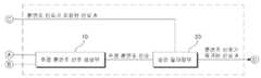
도 1은 종래의 일반적인 혼 변조 신호 제거 장치의 개괄적 구성을 도시한 도면이다.FIG. 1 is a diagram showing a general configuration of a conventional intermodulation signal removing apparatus.
도 1을 참조하면, 종래의 혼 변조 신호 제거 장치는 추정 혼 변조 신호 생성부(10) 및 상관 필터링부(20)를 포함한다.Referring to FIG. 1, a conventional intermodulation signal canceling apparatus includes an estimated intermodulation
종래의 혼 변조 신호 제거 장치에서 추정 혼 변조 신호 생성부(100)는 제1 신호 및 제2 신호를 입력받아 제3 주파수 성분의 추정 혼 변조 신호를 생성한다. 혼 변조 신호를 포함하는 신호 A 및 출력된 추정 혼 변조 신호는 상관 필터링부(20)로 입력되며 상관 필터링부(20)는 신호 A에 포함된 상호 변조 신호를 제거한다.In the conventional intermodulation signal elimination apparatus, the estimated intermodulation signal generation unit 100 receives the first signal and the second signal and generates an estimated intermodulation signal of the third frequency component. The signal A including the intermodulation signal and the output estimated intermodulation signal are input to the
도 2는 종래의 혼 변조 신호 제거 장치에서 혼 변조 신호 생성부의 구조를 도시한 블록도이다.2 is a block diagram showing the structure of a intermodulation signal generation unit in a conventional intermodulation signal elimination apparatus.
도 2를 참조하면, 종래의 혼 변조 신호 생성부는 입력신호 조절부(111), 전원 조절부(121), 출력신호 조절부(141) 등의 여러 가지 조절부와 입력신호 제어부(110), 비선형 제어부(120) 등과 같은 다수의 제어부를 구비한다.2, the conventional intermodulation signal generation unit includes various control units such as an input
종래의 혼 변조 신호 장치의 혼 변조 신호 생성부(100)는 다수의 조절부 및 제어부를 구비하고 있기 때문에 상당한 비용이 소모되는 문제점이 있었다.Since the intermodulation signal generation unit 100 of the conventional intermodulation signal apparatus includes a plurality of adjustment units and a control unit, a considerable cost is consumed.
또한, 제어 동작으로 인해 상당한 시간 지연이 발생하여 실시간 처리가 어려워지는 문제점이 있었다.
In addition, there is a problem that a considerable time delay occurs due to the control operation, which makes real-time processing difficult.
상기한 바와 같은 종래기술의 문제점을 해결하기 위해, 본 발명에서는 제어부 및 조절부를 필요로 하지 않는 혼 변조 신호 제거를 위한 디지털 장치 및 방법을 제안한다.In order to solve the problems of the prior art as described above, the present invention proposes a digital device and method for eliminating intermodulation signal without requiring a control part and an adjusting part.
또한, 본 발명은 혼 변조 신호 제거를 위한 처리 시간을 최소화할 수 있는 혼 변조 신호 제거를 위한 디지털 장치 및 방법을 제안한다.In addition, the present invention proposes a digital apparatus and method for intermodulation signal cancellation capable of minimizing processing time for intermodulation signal elimination.
또한, 본 발명은 짝수 차수 및 홀수 차수의 혼 변조 신호를 모두 제거할 수 있는 혼 변조 신호 제거를 위한 디지털 장치 및 방법을 제안한다.
In addition, the present invention proposes a digital device and a method for eliminating intermodulation signals capable of eliminating both even-order and odd-order intermodulation signals.
상기한 목적을 달성하기 위해 본 발명의 바람직한 일 실시예에 따르면, 혼 변조 신호 제거를 위한 참조 신호와 수신 신호를 기저대역의 신호로 변환하는 디지털 하양 변환기; 상기 디지털 하향 변환기를 통해 출력되는 디지털 기저대역 참조 IQ 신호로부터 짝수 또는 홀수 차수의 혼 변조 재생 신호를 출력하는 혼 변조 신호 재생기; 상기 혼 변조 재생 신호에 대한 준 직교화를 수행하는 준 직교화기; 상기 준 직교화기에서 출력되는 준 직교화 혼 변조 재생 신호와 상기 디지털 하향 변환기로부터 출력되는 디지털 기저대역 수신 IQ 신호에 포함된 혼 변조 신호의 시간적 동기를 일치시키는 혼 변조 신호 추출기; 상기 혼 변조 신호 검출기의 출력 신호와 상기 디지털 기저대역 수신 IQ 신호 상호 상관을 통해 상기 혼 변조 신호 검출기의 출력 신호의 진폭 및 위상을 보상하는 혼 변조 신호 검출기; 및 상기 혼 변조 신호 검출기의 출력 신호를 이용하여 상기 디지털 기저대역 수신 IQ 신호에 포함된 혼 변조 신호를 제거하는 혼 변조 신호 제거기를 포함하는 혼 변조 신호 제거를 위한 디지털 장치가 제공된다.In order to achieve the above object, according to a preferred embodiment of the present invention, there is provided a digital signal processor comprising: a digital-to-analog converter for converting a reference signal and a reception signal for intermodulation signal into a baseband signal; An intermodulation signal regenerator for outputting an even or odd order intermodulation reproduction signal from the digital baseband reference IQ signal outputted through the digital down-converter; A quasi-orthogonalizer for performing quasi orthogonalization on the intermodulation regeneration signal; An intermodulation signal extractor for matching temporal synchronization of a quasi-orthogonal intermodulation reproduction signal output from the quasi-orthogonalizer and an intermodulation signal contained in a digital baseband reception IQ signal output from the digital down-converter; An intermodulation signal detector for compensating for the amplitude and phase of the output signal of the intermodulation signal detector through an inter-correlation of the output signal of the intermodulation signal detector and the digital baseband reception IQ signal; And an intermodulation signal canceller for removing an intermodulation signal included in the digital baseband reception IQ signal using an output signal of the intermodulation signal detector.
상기 혼 변조 신호 재생기는 짝수 차수의 혼 변조 재생 신호의 출력을 위해 테일러 급수를 이용하고 홀수 차수의 혼 변조 재생 신호의 출력을 위해 볼테라 급수를 이용한다.The intermodulation signal regenerator uses the Taylor series for outputting odd-order intermodulation regeneration signals and the Volterra series for outputting odd-order intermodulation regeneration signals.
상기 준 직교화기는 혼 변조 재생 신호에 대한 자기 상관값과 상호 상관값에 대해 준고유값 분해(VSQ-EVD:Variable Simple Quasi-Eigenvalue Decompsition)을 이용하여 준 직교화 계수를 추출한다.The quasi-orthogonalizer extracts a quasi orthogonalization coefficient using a quasi-eigenvalue decomposition (VSQ-EVD) for an autocorrelation value and a cross-correlation value for the intermodulation reproduction signal.
상기 혼 변조 신호 재생기는, 짝수 차후 또는 홀수 차수의 혼 변조 재생 신호를 출력하는 디지털 혼 변조 선택적 차수 재생기; 상기 디지털 혼 변조 선택적 차수 재생기의 출력 신호를 정규화는 디지털 정규화기; 및 상기 디지털 정규화기의 출력 신호에 대핸 저역 통과 필터링을 수행하는 디지털 저역 통과 필터를 포함한다.Wherein the intermodulation signal regenerator includes a digital intermodulation selective order regenerator for outputting even-odd or odd-order intermodulation regeneration signals; Wherein the normalization of the output signal of the digital intermodulation-selective-order regenerator comprises: a digital normalizer; And a digital low-pass filter for performing low-pass filtering on the output signal of the digital normalizer.
상기 준 직교화기는, 상기 혼 변조 재생 신호에 대한 자기 상관값과 상호 상관값을 출력하는 디지털 상관기; 상기 디지털 자기 상관값과 디지털 상호 상관값에 대해 준고유값 분해(VSQ-EVD:Variable Simple Quasi-Eigenvalue Decompsition)을 이용하여 준 직교화 계수를 추출하는 디지털 준 직교화 계수 추출기; 및 상기 디지털 준 직교화 계수를 상기 혼 변조 재생 신호에 적용하여 준 직교화를 수행하는 디지털 준 직교화기를 포함한다.Wherein the quasi-orthogonalizer comprises: a digital correlator for outputting an autocorrelation value and a cross-correlation value for the intermodulation reproduction signal; A digital quasi-orthogonalization coefficient extractor for extracting a quasi orthogonalization coefficient using the digital autocorrelation value and the digital cross-correlation value using Variable Simple Quasi-Eigenvalue Decomposition (VSQ-EVD); And a digital quasi-orthogonalizer for performing quasi orthogonalization by applying the digital quasi-orthogonalization coefficient to the intermodulation reproduction signal.
상기 혼 변조 신호 추출기는, 상기 준 직교화 혼 변조 디지털 재생 신호와 상기 디지털 기저대역 수신 IQ 신호 사이의 상호 상관 연산을 통해 상관성이 가장 큰 샘플의 위치를 획득하는 제2 디지털 상호 상관기; 및 상기 진폭 상관성이 가장 큰 샘플의 위치에 기초하여 상기 준 직교화 혼 변조 재생 신호와 상기 디지털 기저대역 수신 IQ 신호에 포함된 혼 변조 신호간의 시간적 동기를 일치시키는 디지털 지연 보상기를 포함한다.Wherein the intermodulation signal extractor comprises: a second digital correlator for obtaining a position of a sample having the highest correlation through a cross-correlation calculation between the quasi-orthogonal intermodulation digital reproduction signal and the digital baseband reception IQ signal; And a digital delay compensator for matching temporal synchronization between the quasi-orthogonal intermodulation reproduction signal and the intermodulation signal included in the digital baseband reception IQ signal based on the position of the sample having the largest amplitude correlation.
상기 혼 변조 신호 검출기는, 상기 혼 변조 신호 추출기의 출력 신호와 상기 디지털 기저대역 수신 IQ 신호 사이의 상호 상관 연산을 통해 상관성이 큰 진폭값과 위상값을 획득하는 제2 디지털 상호 상관기; 및 상기 상관성이 큰 진폭값 및 위상값을 이용하여 상기 혼 변조 신호 추출기의 출력 신호의 위상 및 진폭을 보상하는 디지털 진폭-위상 보상기를 포함한다.Wherein the intermodulation signal detector comprises: a second digital correlator that obtains an amplitude value and a phase value with high correlation through a cross-correlation calculation between the output signal of the intermodulation signal extractor and the digital baseband reception IQ signal; And a digital amplitude-phase compensator for compensating for the phase and amplitude of the output signal of the intermodulation signal extractor using the correlation value and the phase value having high correlation.
본 발명의 다른 측면에 따르면, 혼 변조 신호 제거를 위한 참조 신호와 수신 신호를 기저대역의 신호로 변환하는 단계(a); 상기 참조 신호를 하향 변환한 디지털 기저대역 참조 IQ 신호로부터 짝수 또는 홀수 차수의 혼 변조 디지털 재생 신호를 출력하는 단계(b); 상기 혼 변조 디지털 재생 신호에 대한 디지털 준 직교화를 수행하는 단계(c); 상기 디지털 준 직교화를 통해 생성되는 준 직교화 혼 변조 디지털 재생 신호와 상기 수신 신호를 하향 변환한 디지털 기저대역 수신 IQ 신호에 포함된 혼 변조 신호의 시간적 동기를 일치시키는 단계(d); 상기 단계(d)에 의한 출력 신호와 상기 디지털 기저대역 수신 IQ 신호의 상호 상관을 통해 상기 단계(d)에 의한 출력 신호의 진폭 및 위상을 보상하는 단계(e); 및 상기 단계(e)의 출력 신호를 이용하여 상기 디지털 기저대역 수신 IQ 신호에 포함된 혼 변조 신호를 제거하는 단계(f)를 포함하는 혼 변조 신호 제거를 위한 디지털 방법이 제공된다.
According to another aspect of the present invention, there is provided a method of detecting an intermodulation signal, comprising: (a) converting a reference signal and a received signal for intermodulation signal removal into a baseband signal; (B) outputting an even or odd order intermodulation digital reproduction signal from the digital baseband reference IQ signal obtained by down-converting the reference signal; Performing digital quadrature orthogonalization on the intermodulation digital reproduction signal (c); (D) synchronizing temporal synchronization of an intermodulation signal included in a quasi-orthogonal intermodulation digital reproduction signal generated through the digital quasi-orthogonalization and a digital baseband reception IQ signal obtained by down-converting the received signal; (E) compensating the amplitude and phase of the output signal according to the step (d) through cross-correlation between the output signal according to the step (d) and the digital baseband reception IQ signal; And (f) removing the intermodulation signal included in the digital baseband received IQ signal using the output signal of step (e).
본 발명에 의하면, 혼 변조 신호 제거 장치가 조절부 및 제어부를 사용하지 않고 디지털 논리회로로 구현될 수 있다.According to the present invention, the intermodulation signal cancellation device can be implemented as a digital logic circuit without using the regulator and the control unit.
또한, 본 발명에 의하면, 혼 변조 신호 제거의 처리 시간을 최소화할 수 있으며 짝수 차수 및 홀수 차수의 혼 변조 신호를 모두 디지털적으로 제거할 수 있는 장점이 있다.
In addition, according to the present invention, it is possible to minimize the processing time of the intermodulation signal cancellation and to digitally remove even-numbered and odd-order intermodulation signals.
도 1은 종래의 일반적인 혼 변조 신호 제거 장치의 개괄적 구성을 도시한 도면.
도 2는 종래의 혼 변조 신호 제거 장치에서 혼 변조 신호 생성부의 구조를 도시한 블록도.
도 3은 본 발명의 일 실시예에 따른 혼 변조 신호 제거 장치가 적용되는 RF 장치의 일례를 도시한 도면.
도 4는 본 발명의 일 실시예에 따른 혼 변조 신호 제거 장치의 개략적 구조를 도시한 도면.
도 5는 본 발명의 일 실시예에 따른 혼 변조 신호 재생기의 구조를 도시한 블록도.
도 6은 본 발명의 일 실시예에 따른 혼 변조 신호 준 직교화기의 구성을 도시한 블록도.
도 7은 본 발명의 일 실시예에 따른 혼 변조 신호 추출기의 구조를 도시한 블록도.
도 8은 본 발명의 일 실시예에 따른 혼 변조 신호 검출기의 구조를 도시한 블록도.
도 9는 본 발명의 일 실시예에 따른 혼 변조 신호 제거기의 구조를 도시한 블록도.
도 10은 본 발명의 일 실시예에 따른 혼 변조 신호 제거 방법의 전체적인 흐름을 도시한 순서도.BRIEF DESCRIPTION OF THE DRAWINGS FIG. 1 is a diagram showing a general configuration of a conventional intermodulation signal removing apparatus. FIG.
2 is a block diagram showing the structure of a intermodulation signal generation unit in a conventional intermodulation signal elimination apparatus.
3 is a diagram illustrating an example of an RF apparatus to which an intermodulation signal eliminator according to an embodiment of the present invention is applied.
4 illustrates a schematic structure of an intermodulation signal removing apparatus according to an embodiment of the present invention.
5 is a block diagram illustrating the structure of an intermodulation signal regenerator according to an embodiment of the present invention.
FIG. 6 is a block diagram showing the configuration of an intermodulation signal quasi-orthogonalizer according to an embodiment of the present invention; FIG.
7 is a block diagram illustrating the structure of an intermodulation signal extractor according to an embodiment of the present invention.
8 is a block diagram illustrating the structure of an intermodulation signal detector according to an embodiment of the present invention.
9 is a block diagram illustrating the structure of an intermodulation signal remover according to an embodiment of the present invention.
FIG. 10 is a flowchart showing an overall flow of an intermodulation signal removing method according to an embodiment of the present invention. FIG.
본 발명은 다양한 변경을 가할 수 있고 여러 가지 실시예를 가질 수 있는 바, 특정 실시예들을 도면에 예시하고 상세한 설명에 상세하게 설명하고자 한다. 그러나, 이는 본 발명을 특정한 실시 형태에 대해 한정하려는 것이 아니며, 본 발명의 사상 및 기술 범위에 포함되는 모든 변경, 균등물 내지 대체물을 포함하는 것으로 이해되어야 한다. 각 도면을 설명하면서 유사한 참조부호를 유사한 구성요소에 대해 사용하였다.While the invention is susceptible to various modifications and alternative forms, specific embodiments thereof are shown by way of example in the drawings and will herein be described in detail. It should be understood, however, that the invention is not intended to be limited to the particular embodiments, but includes all modifications, equivalents, and alternatives falling within the spirit and scope of the invention. Like reference numerals are used for like elements in describing each drawing.
이하에서, 본 발명에 따른 실시예들을 첨부된 도면을 참조하여 상세하게 설명한다.Hereinafter, embodiments according to the present invention will be described in detail with reference to the accompanying drawings.
도 3은 본 발명의 일 실시예에 따른 혼 변조 신호 제거를 위한 디지털 장치가 적용되는 RF 장치의 일례를 도시한 도면이다.3 is a diagram illustrating an example of an RF device to which a digital device for canceling an intermodulation signal according to an embodiment of the present invention is applied.
도 3을 참조하면, 본 발명의 일 실시예에 따른 혼 변조 신호 제거 장치가 적용되는 RF 장치는 제1 수신 포트(300), 송신 포트(302), 제2 수신 포트(304), 송/수신 경로 블록(306), 디지털 혼 변조 신호 제거 장치(310)를 포함할 수 있다.3, an RF apparatus to which an intermodulation signal canceller according to an embodiment of the present invention is applied includes a
본 발명의 혼 변조 신호 제거를 위한 디지털 장치는 혼 변조 신호가 발생하는 다양한 RF 장치에 적용될 수 있다. 예를 들어, 기지국, RRH(Remote Radio Head), AAS(Active Antenna System) 및 중계기 등 송신과 수신이 동시에 이루어지는 다양한 RF 장치에 적용될 수 있다.The digital device for eliminating the intermodulation signal of the present invention can be applied to various RF devices in which intermodulation signals are generated. For example, the present invention can be applied to various RF devices including a base station, a remote radio head (RRH), an active antenna system (AAS), and a repeater.
선택적(홀수/짝수) 차수 혼 변조 신호는 송신과 수신이 동시에 이루어지는 다양한 RF 장치에서 발생할 수 있다. 일반적인 이동통신 시스템에서 송신과 수신은 서로 다른 주파수 대역을 통해 이루어지나 안테나 및 급전선 등의 공용화 수동 소자의 비선형적 특성으로 인해 주파수들간의 선택적(홀수/짝수) 차수 혼 변조를 유발시킨다.Selective (odd / even) order intermodulation signals can occur in various RF devices that transmit and receive simultaneously. In a typical mobile communication system, transmission and reception are performed through different frequency bands. However, due to the non-linear characteristics of the passive components such as antennas and feeder lines, selective (odd / even) intermodulation is caused between frequencies.
혼 변조 신호는 홀수 차수 또는 짝수 차수에서 발생하며, 본 명세서에서는 선택적 차수 혼 변조 신호를 간략히 혼 변조 신호로 정의하여 설명한다.The intermodulation signal occurs in odd order or even order, and in the present specification, a selective order intermodulation signal is simply defined as an intermodulation signal.
도 3을 참조하면, 제1 수신 포트(300)로는 수신 신호가 입력되며, 송신 포트(302)로는 송신 신호가 송신된다. 이때 제1 수신 포트(300)로 입력되는 신호는 수신 신호와 송신 신호로 인해 유발되는 혼 변조 신호가 포함된 신호이다. 제2 수신 포트(304)로는 혼 변조를 유발하는 신호(예를 들어, 송신 신호)가 입력된다. 예를 들어, 제2 수신 포트(300)로는 송신 신호의 일부를 커플링한 신호가 입력된다. 본 명세서에서는 제2 수신 포트(304)로 입력되는 신호를 참조 신호로 정의한다.Referring to FIG. 3, a received signal is input to the
제1 수신 포트(300)를 통해 수신되는 수신 신호 및 제2 수신 포트(304)를 통해 입력되는 참조 신호는 RF 경로 블록(306)을 경유하여 혼 변조 신호 제거 장치(310)로 입력된다.The reception signal received through the
혼 변조 신호 제거를 위한 디지털 장치(310)는 수신 신호 및 참조 신호를 이용하여 수신 신호에 포함된 혼 변조 신호를 디지털적으로 제거하는 기능을 한다. 본 발명의 바람직한 실시예에 따르면, 본 발명의 혼 변조 신호 제거를 위한 디지털 장치(310)는 FPGA를 이용하여 구현되며 어떠한 프로세서도 사용하지 않고 구현된다.The
이하에서는 본 발명의 일 실시예에 따른 혼 변조 신호 제거 장치의 장치의 상세한 구조를 설명한다.Hereinafter, a detailed structure of an apparatus for canceling an intermodulation signal according to an embodiment of the present invention will be described.
도 4는 본 발명의 일 실시예에 따른 혼 변조 신호 제거 장치의 장치의 개략적 구조를 도시한 도면이다.4 is a diagram showing a schematic structure of an apparatus for intermodulation signal elimination apparatus according to an embodiment of the present invention.
도 4를 참조하면, 본 발명의 일 실시예에 따른 혼 변조 신호 제거 장치는 제1 디지털 하향 변환기(400), 제2 디지털 하향 변환기(410), 혼 변조 신호 재생기(500), 혼 변조 신호 준 직교화기(600), 제1 디지털 지연기(700), 제2 디지털 지연기(710), 제3 디지털 지연기(720), 혼 변조 신호 추출기(800), 혼 변조 신호 검출기(900) 및 혼 변조 신호 제거기(1000)를 포함할 수 있다.4, an intermodulation signal cancellation apparatus according to an embodiment of the present invention includes a first
도 4에 도시된 모든 구성 요소들은 디지털 방식으로 신호를 처리하며, 디지털 신호를 출력한다.All of the components shown in FIG. 4 process digital signals and output digital signals.
제1 디지털 하향 변환기(400)로는 참조 신호가 입력되며, 제2 디지털 하향 변환기(410)로는 수신 신호가 입력된다. 전술한 바와 같이, 참조 신호는 송신 신호로부터 커플링된 신호일 수 있다.A reference signal is input to the first
도 4에는 두 개의 디지털 하향 변환기(400, 410)가 구비되는 구성이 도시되어 있으나, 디지털 하향 변환기의 수는 혼 변조를 유발하는 신호의 수에 상응하여 변경될 수 있다. 예를 들어, 서로 다른 두 주파수 대역의 신호가 혼 변조를 유발하게 될 경우 추가적인 디지털 하향 변환기가 구비될 수 있다.Although FIG. 4 illustrates a configuration in which two
필요에 따라, 참조 신호는 디지털 하향 변환기(400)를 거치지 않고 직접 혼 변조 신호 재생기(500)로 입력될 수도 있다.If necessary, the reference signal may be input directly to the
제1 디지털 하향 변환기(400) 및 제2 디지털 하향 변환기(410)는 각각 입력된 신호를 기저 대역의 IQ 디지털 신호로 변환하는 기능을 한다. 제1 디지털 하향 변환기(400)는 참조 신호에 대한 디지털 기저대역 IQ 신호를 출력하며, 제2 디지털 하향 변환기(410)는 수신 신호에 대한 디지털 기저대역 IQ 신호를 출력한다.The first digital down-
제1 디지털 하향 변환기(400)에서 출력되는 참조 신호에 대한 디지털 IQ 신호는 혼 변조 신호 재생기(500)로 입력된다. 혼 변조 신호 재생기(500)는 홀수 또는 짝수 차수의 혼 변조 신호를 재생하는 기능을 한다. 혼 변조 신호 재생기(500)는 정규화된 혼 변조 재생 신호를 출력한다.The digital IQ signal for the reference signal output from the first
정규화된 혼 변조 재생 신호는 혼 변조 신호 준 직교화기(600)로 입력된다. 혼 변조 신호 준 직교화기(600)는 혼 변조 재생 신호에 대해 디지털 준 직교화를 수행한다. 본 발명에서는 프로세서를 사용하지 않고 직교화를 수행하기 위해 준 직교화를 수행하며, 혼 변조 신호 준 직교화기(600)의 상세한 구성은 별도의 도면을 참조하여 설명하기로 한다.The normalized intermodulation reproduction signal is input to the intermodulation
혼 변조 신호 준 직교화기(600)에서 출력되는 준 직교화된 혼 변조 재생 신호는 혼 변조 신호 추출기(800)로 입력된다. 참조 신호에 대한 혼 변조 신호 재생 및 준 직교화가 이루어지는 동안 제2 디지털 하향 변환기(410)를 통해 출력되는 수신 신호에 대한 기저대역 디지털 IQ 신호(디지털 기저대역 수신 IQ 신호)는 제1 디지털 지연기(700)를 통해 지연되며, 제1 디지털 지연기(700)의 출력 신호 역시 혼 변조 신호 추출기(800)로 입력된다.The quasi-orthogonal intermodulation reproduction signal output from the intermodulation
혼 변조 신호 추출기(800)는 주파수 오프셋을 보상하고 수신 신호와 혼 변조 재생 신호간의 시간적 동기를 맞추는 기능을 하며, 혼 변조 신호 추출기(800)는 동기가 보상된 혼 변조 보상 신호를 출력한다.The
제2 디지털 지연기(710)는 혼 변조 신호 추출기(800)에서 주파수 오프셋 보상 연산 및 동기를 맞추는 연산을 수행하는 동안 디지털 기저대역 수신 IQ 신호를 지연시킨다.The second
제2 디지털 지연기(710)에서 출력되는 디지털 기저대역 수신 IQ 신호 및 혼 변조 신호 추출기(800)에서 출력되는 혼 변조 보상 신호는 혼 변조 신호 검출기(900)로 입력된다.The digital baseband reception IQ signal output from the second
혼 변조 신호 검출기(900)는 혼 변조 보상 신호와 디지털 기저대역 수신 IQ 신호에 포함된 혼 변조 신호간의 진폭 및 위상을 일치시키는 기능을 한다.The
제3 디지털 지연기(720)는 혼 변조 신호 검출기(900)에서 진폭 및 위상 보상 연산을 수행하는 동안 디지털 기저대역 수신 IQ 신호를 지연시킨다.The third
제3 디지털 지연기(720)의 출력 신호 및 혼 변조 검출 신호는 혼 변조 신호 제거기(1000)로 입력된다. 혼 변조 신호 제거기(100)는 디지털 기저대역 수신 IQ 신호로부터 혼 변조 신호를 제거하는 기능을 한다. 디지털 기저대역 수신 IQ 신호로부터 혼 변조 신호를 제거함으로써 수신 신호의 신호대 잡음비를 향상시킬 수 있게 된다.The output signal of the third
도 5는 본 발명의 일 실시예에 따른 혼 변조 신호 재생기의 구조를 도시한 블록도이다.5 is a block diagram illustrating the structure of an intermodulation signal regenerator according to an embodiment of the present invention.
도 5를 참조하면, 본 발명의 일 실시예에 따른 혼 변조 신호 재생기(500)는 디지털 사전 지연 보상기(510), 선택적 차수 혼변조 재생기(520), 디지털 정규화기(530) 및 디지털 저역 통과 필터(540)를 포함할 수 있다.5, an
디지털 사전 지연 보상기(510)는 시간 지연을 보상하는 기능을 하며, 선택적 차수 혼 변조 재생기(520)는 참조 신호를 이용하여 디지털 혼 변조 신호를 재생하는 기능을 한다.The digital
본 발명의 바람직한 실시예에 따르면 혼 변조 재생기(520)는 홀수 차수의 혼 변조 신호 및 짝수 차수의 혼 변조 신호를 모두 재생한다. 홀수 차수의 혼 변조 신호는 테일러 급수(Tayler Series)를 이용하여 재생하며, 짝수 차수의 혼 변조 신호는 볼테라 급수(Volterra Series) 를 이용하여 재생한다.According to a preferred embodiment of the present invention, the
디지털 정규화기(530)는 재생되는 혼 변조 신호의 크기에 대한 정규화를 수행하며, 디지털 저역 통과 필터(540)는 정규화된 신호로부터 고주파 성분의 노이즈를 제거하는 기능을 한다. 고주파 노이즈 성분의 제거를 통해 최종적인 혼 변조 재생 신호가 출력된다.The
도 6은 본 발명의 일 실시예에 따른 혼 변조 신호 준 직교화기의 구성을 도시한 블록도이다.6 is a block diagram illustrating a configuration of an intermodulation signal quasi-orthogonalizer according to an embodiment of the present invention.
도 6을 참조하면, 본 발명의 일 실시예에 따른 혼 변조 신호 준 직교화기(600)는 디지털 상관기(610), 디지털 지연기(620), 디지털 준 직교화 계수 추출기(630) 및 디지털 준 직교화기(640)를 포함한다.6, an intermodulation
디지털 상관기(610)는 혼 변조 신호 재생기(500)에서 출력되는 혼 변조 재생 신호에 대한 상관 연산을 수행한다. 구체적으로, 디지털 상관기(610)는 혼 변조 재생 신호에 대해 자기 상관과 상호 상관 연산을 수행한다.The
일례로, N개의 짝수 차수 혼 변조 재생 신호에 대해 N X N개의 디지털 상관값 데이터를 출력하고 M개의 홀수 차수 혼 변조 재생 신호에 대해 M X M개의 디지털 상관값 데이터가 출력된다.For example, N X N digital correlation value data are output for N even-order intermodulation reproduction signals and M X M digital correlation value data are output for M odd-order intermodulation reproduction signals.
디지털 상관값 데이터는 디지털 준 직교화 계수 추출기(630)로 입력되며, 준 직교화 계수 추출 연산 동작동안 디지털 지연기(620)는 혼 변조 재생 신호를 지연시킨다.The digital correlation value data is input to the digital quasi
디지털 상관값 데이터 매트릭스에서 대각 성분에 해당되는 값(디지털 자기 상관 연산에 의한 값)은 정규화된 값을 가진다. 그리고, 대각 성분 이외에 해당되는 값(디지털 상호 상관 연산에 의한 값)은 매우 작은 값이며 매트릭스에서 상삼각 값과 하삼각 값은 위상이 직각인 90도 위상을 가지는 대칭 구조를 가진다. 상호 상관값이 자기 상관값보다 매우 작다는 것은 선택적 차수들간의 상관성이 거의 없다는 것을 의미한다.In the digital correlation value data matrix, a value corresponding to the diagonal component (a value obtained by digital autocorrelation) has a normalized value. The values other than the diagonal components (values obtained by the digital cross-correlation calculation) are very small values, and the upper triangular value and the lower triangular value in the matrix have a symmetric structure with a phase angle of 90 degrees. The fact that the cross-correlation value is much smaller than the autocorrelation value means that there is little correlation between the selective orders.
디지털 준 직교화 계수 추출기(630)는 N X N 상관값 데이터 또는 M X M의 정규 직교화 코드와 디지털 상관값 데이터를 이용하여 준 직교화 계수를 추출하는 연산을 수행한다. 프로세서와 연동하지 않고 직교화 계수를 획득하기 위해 본 발명에서는 준 직교화 계수를 추출하며, 준 직교화 코드 및 디지털 상관값 데이터에 대해 준고유값 분해(VSQ-EVD: Variable Simple Quasi-Eigenvalue Decomposition) 디지털 알고리즘 연산을 수행하여 준 직교화 계수를 추출한다.The digital quasi
준 직교화 코드는 상호 상관이 전혀 없는 정규화된 고유 벡터이며 따라서 자기 상관만 존재하는 코드이다. 그리고 디지털 상관기(510)의 상관값 데이터는 가변되는 간단한 준 고유값 분해 디지털 신호 처리 장치에 필요한 고유값에 해당되는 데이터이다. 가변되는 준 고유값 분해 디지털 처리 장치에 의해 N X N 또는 M X M개의 준 직교화 계수를 추출한다.The quasi-orthogonalization code is a normalized eigenvector with no cross-correlation and thus is only code that is autocorrelated. The correlation value data of the
디지털 준 직교화기(640)는 혼 변조 재생 신호에 직교화 계수를 적용하여 준 직교화를 수행한다. 준 직교화가 수행되었다는 점은 혼 변조 재생 신호에서 선택적 차수간의 자기 상관값은 정규화된 값을 가지고 서로 다른 선택적 차수간의 상호 상관값은 0에 가까운 아주 작은 값을 가진다는 것을 의미한다.The digital
도 7은 본 발명의 일 실시예에 따른 혼 변조 신호 추출기의 구조를 도시한 블록도이다.7 is a block diagram illustrating the structure of an intermodulation signal extractor according to an embodiment of the present invention.
도 7을 참조하면, 본 발명의 일 실시예에 따른 혼 변조 신호 추출기(800)는 디지털 주파수 오프셋 보상기(810), 제1 디지털 상호 상관기(820) 및 디지털 지연 보상기(830)를 포함할 수 있다.7, an
혼 변조 신호 재생기(500)에서는 디지털 저역 통과 필터(540)를 통해 필터링이 이루어지며, 이러한 필터링 동작에 의해 그룹 지연이 발생하게 된다. 디지털 주파수 오프셋 보상기(810)는 준 직교화된 혼 변조 재생 신호에 대한 그룹 지연을 보상하기 위한 주파수 오프셋을 조정한다.In the
제1 디지털 상호 상관기(820)는 주파수 오프셋이 보상된 준 직교화 혼 변조 재생 신호와 디지털 기저대역 수신 IQ 신호에 대한 상호 상관을 연산하고 상호 디지털 진폭 상관성이 가장 큰 샘플의 위치를 구한다. 제1 디지털 상호 상관기(820)에서의 상관 연산은 디지털 기저대역 수신 IQ 신호에 포함된 혼 변조 신호와 혼 변조 재생 신호간의 시간적 동기 일치를 위한 것이다.The first
제1 디지털 상호 상관기(820)는 상호 디지털 진폭 상관성이 가장 큰 샘플의 위치를 출력하게 하며, 디지털 지연 보상기(830)는 상호 상관성이 가장 큰 샘플의 위치에 기초하여 준 직교화된 혼 변조 재생 신호의 지연을 보상한다.The first
혼 변조 신호 추출기(800)를 통해 혼 변조 재생 신호와 디지털 기저대역 수신 IQ 신호 사이의 시간 동기가 이루어지며, 시간 동기가 보상된 혼 변조 보상 신호가 혼 변조 신호 추출기(800)를 통해 출력된다.Time synchronization is performed between the intermodulation reproduction signal and the digital baseband reception IQ signal through the
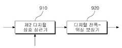
도 8은 본 발명의 일 실시예에 따른 혼 변조 신호 검출기의 구조를 도시한 블록도이다.8 is a block diagram illustrating the structure of an intermodulation signal detector according to an embodiment of the present invention.
도 8을 참조하면, 본 발명의 일 실시예에 따른 혼 변조 신호 검출기는 제2 디지털 상관기(910) 및 디지털 진폭-위상 보상기(920)를 포함할 수 있다.Referring to FIG. 8, an intermodulation signal detector according to an embodiment of the present invention may include a second
제2 디지털 상관기(910)는 혼 변조 보상 신호와 디지털 기저대역 수신 IQ 신호간의 디지털 상관성이 최대가 되는 진폭값과 위상값을 구하여 이를 출력한다.The second
제2 디지털 상관기(910)에 의해 출력되는 진폭값 및 위상값은 디지털 진폭-위상 보상기(920)로 입력되며, 디지털 진폭-위상 보상기(920)는 혼 상관성이 최대가 되는 진폭값 및 위상값에 기초하여 혼 변조 보상 신호의 진폭 및 위상을 디지털 기저대역 수신 IQ 신호의 진폭 및 위상과 일치시키는 기능을 수행한다.The amplitude value and the phase value output by the second
도 9는 본 발명의 일 실시예에 따른 혼 변조 신호 제거기의 구조를 도시한 블록도이다.9 is a block diagram illustrating the structure of an intermodulation signal remover according to an embodiment of the present invention.
도 9를 참조하면, 본 발명의 일 실시예에 따른 혼 변조 신호 제거기는 합산기(1010) 및 차감기(1020)를 포함한다.Referring to FIG. 9, the intermodulation signal canceller according to an embodiment of the present invention includes a
합산기(1010)는 혼 변조 검출 신호를 합산하는 기능을 한다. 예를 들어, 합산기(1010)는 짝수 차수의 혼 변조 신호를 합산하거나 홀수 차수의 혼 변조 신호를 합산하는 기능을 한다.The
차감기(1020)는 디지털 기저대역 수신 IQ 신호로부터 합산된 혼 변조 검출 신호를 차감하는 기능을 한다. 이와 같은 차감기의 차감 동작으로 인해 디지털 기저대역 수신 IQ 신호에 포함된 혼 변조 신호가 제거될 수 있다.The car winding 1020 serves to subtract the intermodulation detection signal summed from the digital baseband received IQ signal. Such a subtracting operation of the secondary winding can eliminate the intermodulation signal included in the digital baseband reception IQ signal.
도 10은 본 발명의 일 실시예에 따른 혼 변조 신호 디지털 제거 방법의 전체적인 흐름을 도시한 순서도이다.FIG. 10 is a flowchart illustrating an overall flow of an intermodulation signal digital cancellation method according to an embodiment of the present invention.
도 10을 참조하면, 수신 신호 및 혼 변조 신호를 유발하는 신호에 대한 참조 신호를 입력받는다(단계 1000).Referring to FIG. 10, a reference signal for a signal causing a reception signal and an intermodulation signal is received (step 1000).
수신 신호 및 참조 신호가 입력되면, 수신 신호 및 참조 신호에 대한 디지털 하향 변환을 각각 수행한다(단계 1002).When the received signal and the reference signal are input, digital down-conversion is performed on the received signal and the reference signal, respectively (step 1002).
디지털 하향 변환이 이루어지면, 참조 신호로부터 혼 변조 재생 신호를 출력한다(단계 1004). 앞서 설명한 바와 같이, 짝수 차수의 혼 변조 재생 신호는 테일러 급수를 이용하여 재생하며, 홀수 차수의 혼 변조 재생 신호는 볼테라 급수를 이용하여 재생한다.When the digital down conversion is performed, the intermodulation reproduction signal is output from the reference signal (step 1004). As described above, the even-order intermodulation reproduction signal is reproduced using the Taylor series, and the odd-order intermodulation reproduction signal is reproduced using the Volterra series.
혼 변조 신호의 재생이 이루어지면, 혼 변조 재생 신호에 대한 준 직교화를 수행한다(단계 1006). 준 직교화는 각 선택적 차수 혼 변조 재생 신호에서 신호간 직교성을 확보하기 위한 작업으로서, 본 발명에서는 프로세서를 활용하지 않고 직교화를 수행하기 위해 준고유값 분해를 이용하여 준 직교화를 수행한다.When the intermodulation signal is reproduced, a quasi-orthogonalization with respect to the intermodulation regeneration signal is performed (step 1006). Quasi orthogonalization is a task for ensuring orthogonality between signals in each selective order intermodulation regeneration signal. In the present invention, quasi orthogonalization is performed using quasi-eigenvalue decomposition to perform orthogonalization without using a processor.
준 직교화가 이루어지면, 하향 변환된 디지털 기저대역 수신 IQ 신호와 준 직교화된 혼 변조 재생 신호간 시간적 동기를 일치시켜 혼 변조 보상 신호가 출력된다(단계 1008).When quasi-orthogonalization is performed, the intermodulation compensation signal is outputted by matching the temporal synchronization between the down-converted digital baseband reception IQ signal and the quasi-orthogonal intermodulation reproduction signal (step 1008).
또한, 동기가 보상된 혼 변조 보상 신호에 대해 디지털 기저대역 수신 IQ 신호와 진폭 및 위상을 일치시키는 동기화 과정을 수행하며, 이를 통해 혼 변조 검출 신호가 출력된다(1010).In addition, a synchronization process of matching the amplitude and phase of the digital baseband reception IQ signal with the synchronization-compensated intermodulation compensation signal is performed, and the intermodulation detection signal is output (1010).
혼 변조 검출 신호가 출력되면, 디지털 기저대역 수신 IQ 신호로부터 혼 변조 검출 신호를 차감하는 작업을 통해 혼 변조 신호가 제거된 수신 신호를 획득한다(단계 1012).When the intermodulation detection signal is output, the intermodulation detection signal is subtracted from the digital baseband reception IQ signal to obtain a reception signal from which the intermodulation signal has been removed (step 1012).
상기에서는 본 발명의 바람직한 실시예를 참조하여 설명하였지만, 해당 기술 분야에서 통상의 지식을 가진 자라면 하기의 특허 청구의 범위에 기재된 본 발명의 사상 및 영역으로부터 벗어나지 않는 범위 내에서 본 발명을 다양하게 수정 및 변경시킬 수 있음을 이해할 수 있을 것이다.
It will be apparent to those skilled in the art that various modifications and variations can be made in the present invention without departing from the spirit or scope of the invention as defined in the appended claims. It will be understood that the invention may be varied and varied without departing from the scope of the invention.
Claims (10)
Translated fromKorean상기 디지털 하향 변환기를 통해 출력되는 디지털 기저대역 참조 IQ 신호로부터 짝수 또는 홀수 차수의 혼 변조 재생 신호를 출력하는 혼 변조 신호 재생기;
상기 혼 변조 재생 신호에 대한 준 직교화를 수행하는 준 직교화기;
상기 준 직교화기에서 출력되는 준 직교화 혼 변조 재생 신호와 상기 디지털 하향 변환기로부터 출력되는 디지털 기저대역 수신 IQ 신호에 포함된 혼 변조 신호의 시간적 동기를 일치시키는 혼 변조 신호 추출기;
상기 혼 변조 신호 추출기의 출력 신호와 상기 디지털 기저대역 수신 IQ 신호 상호 상관을 통해 상기 혼 변조 신호 검출기의 출력 신호의 진폭 및 위상을 보상하는 혼 변조 신호 검출기; 및
상기 혼 변조 신호 검출기의 출력 신호를 이용하여 상기 디지털 기저대역 수신 IQ 신호에 포함된 혼 변조 신호를 제거하는 혼 변조 신호 제거기를 포함하는 것을 특징으로 하는 혼 변조 신호 제거 장치.A digital down-converter for converting a reference signal and a received signal for intermodulation signal elimination into a baseband signal;
An intermodulation signal regenerator for outputting an even or odd order intermodulation reproduction signal from the digital baseband reference IQ signal outputted through the digital down-converter;
A quasi-orthogonalizer for performing quasi orthogonalization on the intermodulation regeneration signal;
An intermodulation signal extractor for matching temporal synchronization of a quasi-orthogonal intermodulation reproduction signal output from the quasi-orthogonalizer and an intermodulation signal contained in a digital baseband reception IQ signal output from the digital down-converter;
An intermodulation signal detector for compensating for the amplitude and phase of the output signal of the intermodulation signal detector through the cross-correlation of the output signal of the intermodulation signal extractor and the digital baseband receive IQ signal; And
And an intermodulation signal canceller for removing an intermodulation signal included in the digital baseband reception IQ signal using an output signal of the intermodulation signal detector.
상기 혼 변조 신호 재생기는 짝수 차수의 혼 변조 재생 신호의 출력을 위해 테일러 급수를 이용하고 홀수 차수의 혼 변조 재생 신호의 출력을 위해 볼테라 급수를 이용하는 것을 특징으로 하는 혼 변조 신호 제거 장치.The method according to claim 1,
Wherein the intermodulation signal regenerator uses a Taylor series for outputting an even-numbered intermodulation reproduction signal and a Volterra series for an odd-order intermodulation reproduction signal.
상기 준 직교화기는 혼 변조 재생 신호에 대한 자기 상관값과 상호 상관값에 대해 준고유값 분해(VSQ-EVD:Variable Simple Quasi-Eigenvalue Decompsition)을 이용하여 준 직교화 계수를 추출하는 것을 특징으로 하는 혼 변조 신호 제거 장치.The method according to claim 1,
Wherein the quasi-orthogonalizer extracts a quasi orthogonalization coefficient using a quasi-eigenvalue decomposition (VSQ-EVD) for an autocorrelation value and a cross-correlation value for the intermodulation reproduction signal Intermodulation signal remover.
상기 혼 변조 신호 재생기는,
짝수 차후 또는 홀수 차수의 혼 변조 재생 신호를 출력하는 디지털 혼 변조 선택적 차수 재생기;
상기 디지털 혼 변조 선택적 차수 재생기의 출력 신호를 정규화는 디지털 정규화기; 및
상기 디지털 정규화기의 출력 신호에 대핸 저역 통과 필터링을 수행하는 디지털 저역 통과 필터를 포함하는 것을 특징으로 하는 혼 변조 신호 제거 장치.3. The method of claim 2,
The intermodulation signal regenerator includes:
A digital intermodulation-selective-order regenerator for outputting even-numbered or odd-order intermodulation regeneration signals;
Wherein the normalization of the output signal of the digital intermodulation-selective-order regenerator comprises: a digital normalizer; And
And a digital low-pass filter for performing low-pass filtering on the output signal of the digital normalizer.
상기 준 직교화기는,
상기 혼 변조 재생 신호에 대한 자기 상관값과 상호 상관값을 출력하는 디지털 상관기;
상기 자기 상관값과 상기 상호 상관값에 대해 준고유값 분해(VSQ-EVD:Variable Simple Quasi-Eigenvalue Decompsition)을 이용하여 준 직교화 계수를 추출하는 준 직교화 계수 추출기; 및
상기 준 직교화 계수를 상기 혼 변조 재생 신호에 적용하여 준 직교화를 수행하는 준 직교화기를 포함하는 것을 특징으로 하는 혼 변조 신호 제거 장치.5. The method of claim 4,
The quasi-orthogonalizer includes:
A digital correlator for outputting an autocorrelation value and a cross-correlation value for the intermodulation reproduction signal;
A quasi orthogonalization coefficient extractor for extracting a quasi orthogonalization coefficient using the autocorrelation value and the cross-correlation value using Variable Simple Quasi-Eigenvalue Decomposition (VSQ-EVD); And
And a quasi orthogonalizer for performing quasi orthogonalization by applying the quasi orthogonalization coefficient to the intermodulation reproduction signal.
상기 혼 변조 신호 추출기는,
상기 준 직교화 혼 변조 재생 신호와 상기 디지털 기저대역 수신 IQ 신호 사이의 상호 상관 연산을 통해 상관성이 가장 큰 샘플의 위치를 획득하는 제2 디지털 상호 상관기; 및
상기 상관성이 가장 큰 샘플의 위치에 기초하여 상기 준 직교화 혼 변조 재생 신호와 상기 디지털 기저대역 수신 IQ 신호에 포함된 혼 변조 신호간의 시간적 동기를 일치시키는 디지털 지연 보상기를 포함하는 것을 특징으로 하는 혼 변조 신호 제거 장치.6. The method of claim 5,
Wherein the intermodulation signal extractor comprises:
A second digital correlator for obtaining a position of a sample having the highest correlation through a cross-correlation calculation between the quasi-orthogonal intermodulation reproduction signal and the digital baseband reception IQ signal; And
And a digital delay compensator for matching the time synchronization between the quasi-orthogonal intermodulation reproduction signal and the intermodulation signal included in the digital baseband reception IQ signal based on the position of the sample having the highest correlation, Modulation signal rejection device.
상기 참조 신호를 하향 변환한 디지털 기저대역 참조 IQ 신호로부터 짝수 또는 홀수 차수의 혼 변조 재생 신호를 출력하는 단계(b);
상기 혼 변조 재생 신호에 대한 준 직교화를 수행하는 단계(c);
상기 준 직교화를 통해 생성되는 준 직교화 혼 변조 재생 신호와 상기 수신 신호를 하향 변환한 디지털 기저대역 수신 IQ 신호에 포함된 혼 변조 신호의 시간적 동기를 일치시키는 단계(d);
상기 단계(d)에 의한 출력 신호와 상기 디지털 기저대역 수신 IQ 신호의 상호 상관을 통해 상기 단계(d)에 의한 출력 신호의 진폭 및 위상을 보상하는 단계(e); 및
상기 단계(e)의 출력 신호를 이용하여 상기 디지털 기저대역 수신 IQ 신호에 포함된 혼 변조 신호를 제거하는 단계(f)를 포함하는 것을 특징으로 하는 혼 변조 신호 제거 방법.(A) converting a reference signal and a received signal for intermodulation signal removal into a baseband signal;
(B) outputting an even or odd-order intermodulation reproduction signal from the digital baseband reference IQ signal obtained by down-converting the reference signal;
(C) performing quasi orthogonalization on the intermodulation reproduction signal;
(D) synchronizing temporal synchronization of an intermodulation signal included in a quasi-orthogonal intermodulation reproduction signal generated through the quasi-orthogonalization and a digital baseband reception IQ signal obtained by down-converting the received signal;
(E) compensating the amplitude and phase of the output signal according to the step (d) through cross-correlation between the output signal according to the step (d) and the digital baseband reception IQ signal; And
And removing (f) the intermodulation signal included in the digital baseband received IQ signal using the output signal of step (e).
상기 단계(b)는 짝수 차수의 혼 변조 재생 신호의 출력을 위해 테일러 급수를 이용하고 홀수 차수의 혼 변조 재생 신호의 출력을 위해 볼테라 급수를 이용하는 것을 특징으로 하는 혼 변조 신호 제거 방법.9. The method of claim 8,
Wherein the step (b) uses a Taylor series for outputting an even-numbered intermodulation reproduction signal and a Volterra series for an odd-order intermodulation reproduction signal.
상기 단계(c)는 혼 변조 재생 신호에 대한 자기 상관값과 상호 상관값에 대해 준고유값 분해(VSQ-EVD:Variable Simple Quasi-Eigenvalue Decompsition)을 이용하여 준 직교화 계수를 추출하는 것을 특징으로 하는 혼 변조 신호 제거 방법.
10. The method of claim 9,
The step (c) is characterized by extracting a quasi orthogonalization coefficient using a quasi-eigenvalue decomposition (VSQ-EVD) for an autocorrelation valueand a cross-correlation value for the intermodulation reproduction signal / RTI >
Priority Applications (1)
| Application Number | Priority Date | Filing Date | Title |
|---|---|---|---|
| KR1020140075021AKR101569726B1 (en) | 2014-06-19 | 2014-06-19 | Method and Device for Canceling Passive Intermodulation Signal |
Applications Claiming Priority (1)
| Application Number | Priority Date | Filing Date | Title |
|---|---|---|---|
| KR1020140075021AKR101569726B1 (en) | 2014-06-19 | 2014-06-19 | Method and Device for Canceling Passive Intermodulation Signal |
Publications (1)
| Publication Number | Publication Date |
|---|---|
| KR101569726B1true KR101569726B1 (en) | 2015-11-18 |
Family
ID=54839165
Family Applications (1)
| Application Number | Title | Priority Date | Filing Date |
|---|---|---|---|
| KR1020140075021AExpired - Fee RelatedKR101569726B1 (en) | 2014-06-19 | 2014-06-19 | Method and Device for Canceling Passive Intermodulation Signal |
Country Status (1)
| Country | Link |
|---|---|
| KR (1) | KR101569726B1 (en) |
Cited By (1)
| Publication number | Priority date | Publication date | Assignee | Title |
|---|---|---|---|---|
| KR101740922B1 (en)* | 2016-02-25 | 2017-05-29 | 주식회사 에이스테크놀로지 | Digital Apparatus and Method for Cancelling Transmitter Leakage Signal |
Citations (1)
| Publication number | Priority date | Publication date | Assignee | Title |
|---|---|---|---|---|
| US20080039045A1 (en) | 2006-08-08 | 2008-02-14 | Daniel F Filipovic | Intermodulation distortion detection and mitigation |
- 2014
- 2014-06-19KRKR1020140075021Apatent/KR101569726B1/ennot_activeExpired - Fee Related
Patent Citations (1)
| Publication number | Priority date | Publication date | Assignee | Title |
|---|---|---|---|---|
| US20080039045A1 (en) | 2006-08-08 | 2008-02-14 | Daniel F Filipovic | Intermodulation distortion detection and mitigation |
Cited By (1)
| Publication number | Priority date | Publication date | Assignee | Title |
|---|---|---|---|---|
| KR101740922B1 (en)* | 2016-02-25 | 2017-05-29 | 주식회사 에이스테크놀로지 | Digital Apparatus and Method for Cancelling Transmitter Leakage Signal |
Similar Documents
| Publication | Publication Date | Title |
|---|---|---|
| US10389313B2 (en) | Distributed antenna system architectures | |
| KR101492381B1 (en) | Linearization for a single power amplifier in a multi-band transmitter | |
| CN104852752B (en) | System and method for self-interference cancellation in efficient full-duplex communication | |
| US8982995B1 (en) | Communication device and method of multipath compensation for digital predistortion linearization | |
| EP3531565B1 (en) | Tower top device and passive intermodulation cancellation method | |
| KR100902336B1 (en) | Co-channel repeater and method | |
| US20100329387A1 (en) | Wireless communication apparatus and wireless communication method | |
| US20150036771A1 (en) | Device and method for communication correction | |
| KR20070106363A (en) | Apparatus and method for canceling multipath interference using multiple wire feedback signals | |
| US9660673B2 (en) | Apparatus and method for canceling inter-modulation products | |
| US11563493B2 (en) | Remote radio unit and central unit for multiple-input multiple-output system | |
| KR102244582B1 (en) | Apparatus For Calibration of Active Array Antenna | |
| JP5883046B2 (en) | Multi-antenna wireless relay system and feedback interference cancellation method using the same | |
| KR101569726B1 (en) | Method and Device for Canceling Passive Intermodulation Signal | |
| JPWO2020144889A1 (en) | Control device and wireless communication device | |
| KR101868848B1 (en) | Device for Canceling Passive Intermodulation Signal | |
| KR101740922B1 (en) | Digital Apparatus and Method for Cancelling Transmitter Leakage Signal | |
| KR100404385B1 (en) | Signal processing method of wireless communication systems by using DSP and apparatus thereof | |
| KR101090766B1 (en) | On-channel repeaters and its method | |
| KR101924229B1 (en) | multiple intermodulation canceling device and its method | |
| KR20170001596A (en) | Method and apparatus for tuning finite impulse response filter in in-band full duplex transceiver | |
| KR100311522B1 (en) | Distortion Signal Compensation Method and Device in Digital TV | |
| KR101431528B1 (en) | Full Band Duplexer and Radio Communication System Therefor | |
| CN119817064A (en) | A communication method and device |
Legal Events
| Date | Code | Title | Description |
|---|---|---|---|
| PA0109 | Patent application | St.27 status event code:A-0-1-A10-A12-nap-PA0109 | |
| PA0201 | Request for examination | St.27 status event code:A-1-2-D10-D11-exm-PA0201 | |
| D13-X000 | Search requested | St.27 status event code:A-1-2-D10-D13-srh-X000 | |
| D14-X000 | Search report completed | St.27 status event code:A-1-2-D10-D14-srh-X000 | |
| PE0902 | Notice of grounds for rejection | St.27 status event code:A-1-2-D10-D21-exm-PE0902 | |
| E13-X000 | Pre-grant limitation requested | St.27 status event code:A-2-3-E10-E13-lim-X000 | |
| P11-X000 | Amendment of application requested | St.27 status event code:A-2-2-P10-P11-nap-X000 | |
| P13-X000 | Application amended | St.27 status event code:A-2-2-P10-P13-nap-X000 | |
| R17-X000 | Change to representative recorded | St.27 status event code:A-3-3-R10-R17-oth-X000 | |
| R17-X000 | Change to representative recorded | St.27 status event code:A-3-3-R10-R17-oth-X000 | |
| PE0701 | Decision of registration | St.27 status event code:A-1-2-D10-D22-exm-PE0701 | |
| GRNT | Written decision to grant | ||
| PR0701 | Registration of establishment | St.27 status event code:A-2-4-F10-F11-exm-PR0701 | |
| PR1002 | Payment of registration fee | Fee payment year number:1 St.27 status event code:A-2-2-U10-U11-oth-PR1002 | |
| PG1601 | Publication of registration | St.27 status event code:A-4-4-Q10-Q13-nap-PG1601 | |
| FPAY | Annual fee payment | Payment date:20181023 Year of fee payment:4 | |
| PR1001 | Payment of annual fee | Fee payment year number:4 St.27 status event code:A-4-4-U10-U11-oth-PR1001 | |
| PR1001 | Payment of annual fee | Fee payment year number:5 St.27 status event code:A-4-4-U10-U11-oth-PR1001 | |
| R18-X000 | Changes to party contact information recorded | St.27 status event code:A-5-5-R10-R18-oth-X000 | |
| PR1001 | Payment of annual fee | Fee payment year number:6 St.27 status event code:A-4-4-U10-U11-oth-PR1001 | |
| PR1001 | Payment of annual fee | Fee payment year number:7 St.27 status event code:A-4-4-U10-U11-oth-PR1001 | |
| PC1903 | Unpaid annual fee | Not in force date:20221112 Payment event data comment text:Termination Category : DEFAULT_OF_REGISTRATION_FEE St.27 status event code:A-4-4-U10-U13-oth-PC1903 | |
| PC1903 | Unpaid annual fee | Ip right cessation event data comment text:Termination Category : DEFAULT_OF_REGISTRATION_FEE Not in force date:20221112 St.27 status event code:N-4-6-H10-H13-oth-PC1903 | |
| R18-X000 | Changes to party contact information recorded | St.27 status event code:A-5-5-R10-R18-oth-X000 |