KR101569337B1 - Touch detecting apparatus and method - Google Patents
Touch detecting apparatus and methodDownload PDFInfo
- Publication number
- KR101569337B1 KR101569337B1KR1020140063176AKR20140063176AKR101569337B1KR 101569337 B1KR101569337 B1KR 101569337B1KR 1020140063176 AKR1020140063176 AKR 1020140063176AKR 20140063176 AKR20140063176 AKR 20140063176AKR 101569337 B1KR101569337 B1KR 101569337B1
- Authority
- KR
- South Korea
- Prior art keywords
- capacitance
- sensor pad
- switch
- driving
- voltage
- Prior art date
- Legal status (The legal status is an assumption and is not a legal conclusion. Google has not performed a legal analysis and makes no representation as to the accuracy of the status listed.)
- Expired - Fee Related
Links
Images


Classifications
- G—PHYSICS
- G06—COMPUTING OR CALCULATING; COUNTING
- G06F—ELECTRIC DIGITAL DATA PROCESSING
- G06F3/00—Input arrangements for transferring data to be processed into a form capable of being handled by the computer; Output arrangements for transferring data from processing unit to output unit, e.g. interface arrangements
- G06F3/01—Input arrangements or combined input and output arrangements for interaction between user and computer
- G06F3/03—Arrangements for converting the position or the displacement of a member into a coded form
- G06F3/041—Digitisers, e.g. for touch screens or touch pads, characterised by the transducing means
- G06F3/044—Digitisers, e.g. for touch screens or touch pads, characterised by the transducing means by capacitive means
- G—PHYSICS
- G06—COMPUTING OR CALCULATING; COUNTING
- G06F—ELECTRIC DIGITAL DATA PROCESSING
- G06F3/00—Input arrangements for transferring data to be processed into a form capable of being handled by the computer; Output arrangements for transferring data from processing unit to output unit, e.g. interface arrangements
- G06F3/01—Input arrangements or combined input and output arrangements for interaction between user and computer
- G06F3/03—Arrangements for converting the position or the displacement of a member into a coded form
- G06F3/041—Digitisers, e.g. for touch screens or touch pads, characterised by the transducing means
- G06F3/0416—Control or interface arrangements specially adapted for digitisers
- G06F3/0418—Control or interface arrangements specially adapted for digitisers for error correction or compensation, e.g. based on parallax, calibration or alignment
- G06F3/04182—Filtering of noise external to the device and not generated by digitiser components
- H—ELECTRICITY
- H03—ELECTRONIC CIRCUITRY
- H03K—PULSE TECHNIQUE
- H03K17/00—Electronic switching or gating, i.e. not by contact-making and –breaking
- H03K17/94—Electronic switching or gating, i.e. not by contact-making and –breaking characterised by the way in which the control signals are generated
- H03K17/96—Touch switches
- H03K17/962—Capacitive touch switches
- H—ELECTRICITY
- H03—ELECTRONIC CIRCUITRY
- H03K—PULSE TECHNIQUE
- H03K2217/00—Indexing scheme related to electronic switching or gating, i.e. not by contact-making or -breaking covered by H03K17/00
- H03K2217/94—Indexing scheme related to electronic switching or gating, i.e. not by contact-making or -breaking covered by H03K17/00 characterised by the way in which the control signal is generated
- H03K2217/96—Touch switches
- H03K2217/9607—Capacitive touch switches
- H03K2217/960735—Capacitive touch switches characterised by circuit details
Landscapes
- Engineering & Computer Science (AREA)
- General Engineering & Computer Science (AREA)
- Theoretical Computer Science (AREA)
- Human Computer Interaction (AREA)
- Physics & Mathematics (AREA)
- General Physics & Mathematics (AREA)
- Position Input By Displaying (AREA)
Abstract
Translated fromKoreanDescription
Translated fromKorean본 발명은 터치 검출 장치 및 방법에 관한 것으로, 보다 상세하게는, 선형성이 보장되고 정전용량의 포화가 방지되면서도 터치 여부 검출의 민감도 악화가 없는 터치 검출 장치 및 방법에 관한 것이다.The present invention relates to a touch detection apparatus and method, and more particularly, to a touch detection apparatus and method without linearity deterioration of touch detection, while preventing saturation of capacitance.
터치 스크린 패널은 영상 표시 장치의 화면에 표시된 문자나 도형을 사람의 손가락이나 다른 접촉수단으로 접촉하여 사용자의 명령을 입력하는 장치로서, 영상 표시 장치 위에 부착되어 사용된다. 터치 스크린 패널은 사람의 손가락 등으로 접촉된 접촉 위치를 전기적 신호로 변환한다. 상기 전기적 신호는 입력 신호로서 이용된다.The touch screen panel is a device for inputting a command of a user by touching a character or a figure displayed on the screen of the image display device with a finger or other contact means of a person, and is attached and used on the image display device. The touch screen panel converts a contact position that is touched by a human finger or the like into an electrical signal. The electrical signal is used as an input signal.
도 1은 종래 기술에 따른 정전식 터치 스크린 패널의 일 예에 관한 분해 평면도이다.1 is an exploded top view of an example of a conventional capacitive touch screen panel.
도 1을 참고하면, 터치 스크린 패널(10)은 투명 기판(12)과 투명 기판(12) 위에 차례로 형성된 제1 센서 패턴층(13), 제1 절연막층(14), 제2 센서 패턴층(15) 및 제2 절연막층(16)과 금속 배선(17)으로 이루어진다.1, a
제1 센서 패턴층(13)은 투명 기판(12) 위에 횡방향을 따라 연결될 수 있으며, 행 단위로 금속 배선(17)과 연결된다.The first
제2 센서 패턴층(15)은 제1 절연막층(14) 위에 열방향을 따라 연결될 수 있으며, 제1 센서 패턴층(13)과 중첩되지 않도록 제1 센서 패턴층(13)과 교호로 배치된다. 또한, 제2 센서 패턴층(15)은 열 단위로 금속 배선(17)과 연결된다.The second
터치 스크린 패널(10)에 사람의 손가락이나 접촉 수단이 접촉되면 제1 및 제2 센서 패턴층(13, 15) 및 금속 배선(17)을 통하여 구동 회로 측으로 접촉 위치에 따른 정전용량의 변화가 전달된다. 그리고 이렇게 전달된 정전용량의 변화가 전기적 신호로 변환됨에 따라 접촉 위치가 파악된다.When a human finger or a contact means is brought into contact with the
그러나 이러한 터치 스크린 패널(10)은 각 센서 패턴층(13, 15)에 인듐-틴 옥사이드(ITO)와 같은 투명한 도전성 물질로 이루어진 패턴을 별도로 구비하여야 하고, 센서 패턴층(13, 15) 사이에 절연막층(14)을 구비하여야 하므로 두께가 증가한다.However, the
또한, 터치에 의해 미세하게 발생하는 정전용량의 변화를 수차례 축적하여야 터치 검출이 가능하기 때문에 높은 주파수로 정전용량 변화를 감지하여야 한다. 그리고, 정전용량의 변화를 정해진 시간 내에 충분히 축적하기 위해서는 낮은 저항을 유지하기 위한 금속 배선을 필요로 하는데, 이러한 금속 배선은 터치 스크린의 테두리에 베젤을 두껍게 하고 추가의 마스크 공정을 발생시킨다.In addition, since the touch detection can be performed by accumulating the changes of capacitance slightly generated by the touch several times, it is necessary to detect the capacitance change at a high frequency. In order to sufficiently accumulate the capacitance change within a predetermined time, a metal wiring is required to maintain a low resistance, which thickens the bezel at the edge of the touch screen and generates an additional mask process.
이러한 문제점을 해결하기 위해 도 2에 도시되는 바와 같은 터치 검출 장치가 제안되었다.To solve this problem, a touch detection apparatus as shown in Fig. 2 has been proposed.
도 2에 도시되는 터치 검출 장치는 터치 패널(20)과 구동 장치(30) 및 이 둘을 연결하는 회로 기판(40)을 포함한다.2 includes a
터치 패널(20)은 기판(21) 위에 형성되며 다각형의 매트릭스 형태로 배열되는 복수의 센서 패드(22) 및 센서 패드(22)에 연결되어 있는 복수의 신호 배선(23)을 포함한다.The
각 신호 배선(23)은 한쪽 끝이 센서 패드(22)에 연결되어 있으며 다른 쪽 끝은 기판(21)의 아래 가장자리까지 뻗어 있다. 센서 패드(22)와 신호 배선(23)은 커버 유리(50)에 패터닝 될 수 있다.Each
구동 장치(30)는 복수의 센서 패드(22)를 순차적으로 하나씩 선택하여 해당 센서 패드(22)의 정전용량을 측정하고, 이를 통해 터치 발생 여부를 검출해낸다.The
터치가 발생하면 터치 발생 도구(예를 들면, 손가락)와 센서 패드(22) 사이에는 터치 정전용량이 형성되는데, 센서 패드(22)에 소정의 신호를 입력하면 터치 정전용량의 존부에 따라 센서 패드(22)로부터의 출력 신호가 달라지게 된다. 구동 장치(30)는 센서 패드(22)로부터의 출력 신호를 통해 터치 발생 여부를 판단하게 된다.When a touch occurs, a touch capacitance is formed between the touch generating tool (e.g., a finger) and the
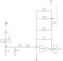
도 3은 본 발명의 일 실시예에 따른 터치 검출 장치의 동작을 설명하기 위한 회로도이다.3 is a circuit diagram for explaining the operation of the touch detection apparatus according to an embodiment of the present invention.
도 3을 참조하면, 터치 검출 장치는 센서패드(22), 구동 정전용량(Cdrv), 연산 증폭기(OP-amp), 아날로그-디지털 변환기(ADC)를 포함할 수 있다. 구동 정전용량(Cdrv), 연산 증폭기(OP-amp), 아날로그-디지털 변환기(ADC)는 도 2의 구동 장치(30)에 포함되는 구성요소이다.Referring to FIG. 3, the touch detection apparatus may include a
연산 증폭기(OP-amp)의 제1 입력단은 센서패드(22)의 출력과 연결되고 제2 입력단에는 기준 전압(Vref)이 인가된다. 연산 증폭기(OP-amp)의 제1 입력단과 출력단 사이에는 구동 정전용량(Cdrv)이 연결되며, 구동 정전용량(Cdrv) 양단의 전위는 제1 스위치(SW1)에 의해 제어된다. 한편, 연산 증폭기(OP-amp)의 제1 입력단과 센서패드(22) 출력단 사이에는 제2 스위치(SW2)가 연결된다.The first input terminal of the operational amplifier OP-amp is connected to the output of the
제1 스위치(SW1)와 제2 스위치(SW1)는 교번하여 온/오프 되는데, 제1 스위치(SW1)가 온 되면, 센서패드(22)와 터치 발생 도구 사이의 터치 정전용량(Ct)이 그라운드 전위로 연결된다. 또한, 센서패드(22) 또는 신호배선 등에 의해 형성되는 기생 정전용량(Cp) 양단 또한 그라운드 전위와 연결된다. 제1 스위치(SW1)의 온에 의해 터치 정전용량(Ct), 기생 정전용량(Cp), 구동 정전용량(Cdrv)이 리셋되며, 구동 정전용량(Cdrv)의 양단 전위는 모두 기준 전압(Vref)과 같아진다.The first switch SW1 and the second switch SW1 are alternately turned on and off. When the first switch SW1 is turned on, the touch capacitance Ct between the
제1 스위치(SW1)가 오프 되고, 제2 스위치(SW2)가 온 상태로 전환된 후 정상 상태에 도달하면, 터치 정전용량(Ct)과 기생 정전용량(Cp)이 모두 기준 전압(Vref)으로 충전되고, 연산 증폭기(OP-amp)에 의해 터치 정전용량(Ct)과 기생 정전용량(Cp)에 충전된 전하의 합과 동일한 양의 전하가 구동 정전용량(Cdrv)에 충전된다. 이는 다음과 같은 수학식으로 표현될 수 있다.When the first switch SW1 is turned off and the second switch SW2 is switched to the on state and then reaches the steady state, both the touch capacitance Ct and the parasitic capacitance Cp become the reference voltage Vref And the same amount of charge as the sum of the charges charged in the touch capacitance Ct and the parasitic capacitance Cp by the operational amplifier OP-amp is charged in the driving capacitance Cdrv. This can be expressed by the following equation.

상기 수학식 1에서 좌변은 터치 정전용량(Ct)과 기생 정전용량(Cp)에 충전된 전하량의 합을 나타내고, 우변은 구동 정전용량(Cdrv)에 충전된 전하량을 나타낸다.In the equation (1), the left side represents the sum of the charge amount charged in the touch capacitance Ct and the parasitic capacitance Cp, and the right side represents the charge amount charged in the drive capacitance Cdrv.
상기 수학식 1에 따라 구동 정전용량(Cdrv)의 양단 전압은 다음과 같이 표현될 수 있다.The voltage across the driving capacitance Cdrv according to Equation (1) can be expressed as follows.

제2 스위치(SW2)가 온 되기 전 구동 정전용량(Cdrv) 양단의 전위차는 0V이므로, 터치 전후 연산 증폭기(OP-amp)의 출력단 전압의 변화량(ΔVo)은 상기 구동 정전용량(Cdrv) 양단의 전압(Vdrv)과 같아진다.The amount of change ΔVo of the output terminal voltage of the operational amplifier OP-amp before and after the touch is equal to the voltage difference between the both ends of the drive capacitance Cdrv before the second switch SW2 is turned on, And becomes equal to the voltage Vdrv.
구동 정전용량(Cdrv), 기준 전압(Vref)은 일정한 값을 가지므로, 연산 증폭기(OP-amp) 출력단 전압의 변화량(△Vo), 즉, 레벨 시프트 값은 터치 정전용량(Ct)에 비례하게 되므로, 터치 검출에 있어서의 선형성이 확보될 수 있다.Since the driving capacitance Cdrv and the reference voltage Vref have a constant value, the change amount? Vo of the output voltage of the operational amplifier OP-amp, that is, the level shift value is proportional to the touch capacitance Ct So that the linearity in touch detection can be secured.
그러나, 상기 수학식 2에서 알 수 있는 바와 같이, 터치 정전용량(Ct)뿐만 아니라 기생 정전용량(Cp) 또한 터치 여부 검출에 영향을 주기 때문에, 터치 검출의 정확성이 떨어지게 된다.However, as can be seen from Equation (2), since not only the touch capacitance Ct but also the parasitic capacitance Cp also affect the touch detection, the accuracy of the touch detection is deteriorated.
또한, 구동 정전용량(Cdrv)이 작을수록 레벨 시프트 값이 커지므로 터치 여부 검출의 민감도가 커지게 되는데, 구동 정전용량(Cdrv)을 작게 형성하게 되면 정상 상태에서 포화가 발생할 우려가 있다.Further, since the level shift value becomes larger as the driving capacitance Cdrv is smaller, the sensitivity of touch detection is increased. If the driving capacitance Cdrv is made small, saturation may occur in a normal state.
따라서, 터치 전후의 레벨 시프트값과 터치 정전용량 간의 선형성이 확보되면서도 기생 정전용량의 영향을 최소화하며, 터치 발생 여부 검출의 민감도를 유지하면서도 정상 상태에서의 포화를 방지할 수 있는 기술이 필요하다.Accordingly, there is a need for a technique capable of minimizing the influence of the parasitic capacitance while maintaining the linearity between the level shift value before and after the touch and the touch capacitance, and preventing the saturation in the steady state while maintaining the sensitivity of touch detection.
본 발명이 해결하고자 하는 과제는 레벨 시프트값과 터치 정전용량 간의 선형성이 보장되고, 정전용량의 포화가 방지되면서도 터치 여부 검출의 민감도가 저하되지 않는 터치 검출 장치 및 방법을 제공하는 것이다.SUMMARY OF THE INVENTION It is an object of the present invention to provide a touch detection apparatus and method in which the linearity between a level shift value and a touch capacitance is ensured and saturation of a capacitance is prevented and sensitivity of touch detection is not deteriorated.
또한, 본 발명의 다른 목적은 선형성이 보장되면서도 기생 정전용량의 영향이 최소화된 터치 검출 장치 및 방법을 제공하는 것이다.It is another object of the present invention to provide a touch detection apparatus and method with minimized influence of parasitic capacitance while ensuring linearity.
본 발명의 또 다른 목적은 회로 내에서 로우 패스 필터가 구현될 수 있도록 함으로써 외부 노이즈의 영향이 제거되고, 터치 발생에 따른 응답 시간 저하가 방지되는 터치 검출 장치 및 방법을 제공하는 것이다.It is still another object of the present invention to provide a touch detection apparatus and method in which a low-pass filter can be implemented in a circuit, thereby eliminating the influence of external noise and preventing a decrease in response time due to generation of a touch.
상술한 목적을 달성하기 위한 본 발명의 일 실시예에 따르면, 터치 입력 도구와의 관계에서 터치 정전용량을 형성하는 센서패드; 상기 센서패드의 출력단과 연결된 제1 입력단 및 기준 전압을 수신하는 제2 입력단을 가지며, 터치 여부에 따라 서로 다른 신호를 출력하는 연산 증폭기; 상기 연산 증폭기의 제1 입력단과 출력단 사이에 연결된 구동 정전용량 양단의 전위를 제어하는 제1 스위치; 상기 센서패드의 출력단과 상기 연산 증폭기의 제1 입력단 간의 연결을 스위칭하며, 상기 제1 스위치와 교번하여 온/오프되는 제2 스위치; 및 상기 구동 정전용량에 선택적으로 정전용량을 병렬 또는 직렬로 부가하여, 상기 구동 정전용량과 전하를 공유하는 구동 정전용량 포화 방지부를 포함하는, 터치 검출 장치가 제공된다.According to an aspect of the present invention, there is provided a touch pad device including: a sensor pad for forming a touch capacitance in relation to a touch input tool; An operational amplifier having a first input terminal connected to the output terminal of the sensor pad and a second input terminal receiving the reference voltage, A first switch for controlling a potential at both ends of a driving capacitance connected between a first input terminal and an output terminal of the operational amplifier; A second switch for switching a connection between an output terminal of the sensor pad and a first input terminal of the operational amplifier and being turned on / off alternately with the first switch; And a driving capacitance saturation preventing unit that adds a capacitance to the driving capacitance in parallel or in series to share the electric charge with the driving capacitance.
상기 구동 정전용량 포화 방지부는, 포화 방지 정전용량; 상기 제2 스위치가 온 상태일 때 상기 포화 방지 정전용량을 상기 구동 정전용량과 병렬 연결시키는 제3 스위치; 및 상기 제2 스위치 및 제3 스위치가 오프 상태일 때 상기 포화 방지 정전용량 양단을 동전위로 제어하여 상기 포화 방지 정전용량의 전하가 상기 구동 정전용량으로 이동할 수 있도록 하는 제4 스위치를 더 포함할 수 있다.The driving capacitance saturation preventing unit may include: a saturation preventing capacitance; A third switch for connecting the anti-saturation capacitance with the driving capacitance in parallel when the second switch is on; And a fourth switch for controlling the both terminals of the saturation-preventing capacitance when the second switch and the third switch are in an off state so that the charge of the saturation-preventing electrostatic capacitance can move to the driving capacitance have.
상기 연산 증폭기의 제2 입력단에는 초과 전압이 인가되며, 상기 제2 스위치가 온 상태로 전환된 후 일정 시간 경과 후에는 상기 초과 전압보다 낮은 기준 전압이 인가될 수 있다.An excess voltage is applied to the second input terminal of the operational amplifier and a reference voltage lower than the excess voltage may be applied after a predetermined time elapses after the second switch is turned on.
상기 터치 검출 장치는, 상기 연산 증폭기의 제2 입력단에 상기 초과 전압과 상기 기준 전압이 선택적으로 인가되도록 제어하는 제5 스위치를 더 포함할 수 있다.The touch detection apparatus may further include a fifth switch for selectively applying the excess voltage and the reference voltage to a second input terminal of the operational amplifier.
상기 터치 검출 장치는, 상기 센서패드의 출력 전압과 상기 기준 전압을 비교하여, 상기 센서패드의 출력 전압이 상기 기준 전압 이상이 될 때에는 상기 연산 증폭기의 제2 입력단에 상기 기준 전압이 인가되도록 상기 제5 스위치를 제어하는 비교기를 더 포함할 수 있다.Wherein the touch detection device compares the output voltage of the sensor pad with the reference voltage so that the reference voltage is applied to the second input terminal of the operational amplifier when the output voltage of the sensor pad becomes equal to or greater than the reference voltage, 5 < / RTI > switch.
상기 터치 검출 장치는, 상기 제2 스위치가 온 상태일 때 상기 센서패드와 연결된 기생 정전용량 또는 상기 터치 정전용량 중 적어도 일부를 충전시키는 기생 정전용량 보상 회로를 더 포함할 수 있다.The touch detection apparatus may further include a parasitic capacitance compensation circuit that charges at least a part of the parasitic capacitance connected to the sensor pad or the touch capacitance when the second switch is in an on state.
상기 기생 정전용량 보상 회로는, 상기 제2 스위치가 온 상태일 때 일단이 상기 센서패드와 연결되며 타단에는 피드백 전압이 공급되는 피드백 정전용량을 포함할 수 있다.The parasitic capacitance compensation circuit may include a feedback capacitance whose one end is connected to the sensor pad when the second switch is on and the feedback voltage is supplied to the other end.
상기 터치 검출 장치는, 상기 센서패드의 출력 전압과 동일한 전압을 다른 센서패드에 인가하는 기생 정전용량 제거 회로를 더 포함할 수 있다.The touch detection apparatus may further include a parasitic capacitance elimination circuit for applying a voltage equal to an output voltage of the sensor pad to another sensor pad.
상기 기생 정전용량 제거 회로는, 상기 제1 스위치가 온 상태일 때에는 그라운드 전압, 상기 제2 스위치가 온 상태일 때에는 상기 기준 전압과 동일한 크기의 전압을 상기 다른 센서패드에 인가할 수 있다.The parasitic capacitance elimination circuit may apply a ground voltage to the other sensor pad when the first switch is in the on state and a voltage of the same magnitude as the reference voltage when the second switch is in the on state.
한편, 본 발명의 다른 실시예에 따르면, 터치 입력 도구와의 관계에서 터치 정전용량을 형성하는 센서패드, 일단에 기준 전압이 공급되는 구동 정전용량 및 상기 구동 정전용량과 병렬 연결되는 포화 방지 정전용량을 초기화시키는 단계; 상기 센서패드 출력단을 상기 구동 정전용량의 일단과 연결시켜, 상기 구동 정전용량과 상기 포화 방지 정전용량이 충전될 수 있도록 하는 단계; 상기 센서패드 출력단과 상기 구동 정전용량 간의 연결을 차단하고, 상기 포화 방지 정전용량에 충전된 전하를 상기 구동 정전용량으로 이동시키는 단계; 및 상기 구동 정전용량의 타단 전압 변동분을 기초로 터치 여부를 검출하는 단계를 포함하는, 터치 검출 방법이 제공된다.According to another embodiment of the present invention, there is provided a touch input device including a sensor pad for forming a touch capacitance in relation to a touch input tool, a driving capacitance for supplying a reference voltage to one end of the sensor pad, ; Connecting the output terminal of the sensor pad to one end of the driving electrostatic capacitance so that the driving electrostatic capacitance and the saturation preventing electrostatic capacitance can be charged; Blocking the connection between the output terminal of the sensor pad and the driving electrostatic capacitance and moving the charge charged in the saturation preventing electrostatic capacitance to the driving electrostatic capacitance; And detecting whether or not the touch is detected based on the other end voltage variation of the drive capacitance.
상기 포화 방지 정전용량의 전하를 이동시키는 단계는, 상기 포화 방지 정전용량의 일단과 상기 구동 정전용량의 일단 간 연결을 차단하고, 상기 포화 방지 정전용량의 양단을 동전위로 제어하는 단계를 포함할 수 있다.The step of transferring the charge of the saturation-preventing electrostatic capacitance may include the step of blocking connection between one end of the saturation-preventing electrostatic capacitance and one end of the driving electrostatic capacitance, and controlling both ends of the anti- have.
상기 포화 방지 정전용량과 구동 정전용량의 충전 단계는, 상기 구동 정전용량 일단에 초과 전압 및 상기 초과 전압보다 낮은 기준 전압을 인가하는 단계를 포함할 수 있다.The step of charging the saturated anti-static capacitance and the driving electrostatic capacitance may include applying an over-voltage and a reference voltage lower than the over-voltage to one end of the driving capacitance.
상기 포화 방지 정전용량과 구동 정전용량의 충전 단계는, 상기 센서패드의 출력 전압과 상기 기준 전압을 비교하여, 상기 센서패드의 출력 전압이 상기 기준 전압 이상이 될 때 상기 기준 전압을 인가하는 단계를 포함할 수 있다.The step of charging the saturation preventing capacitance and the driving electrostatic capacitance may include the step of comparing the output voltage of the sensor pad with the reference voltage and applying the reference voltage when the output voltage of the sensor pad becomes equal to or higher than the reference voltage .
상기 포화 방지 정전용량과 구동 정전용량의 충전 단계는, 기생 정전용량 보상 회로를 통해 상기 센서패드와 연결된 기생 정전용량 또는 상기 터치 정전용량 중 적어도 일부를 충전시키는 단계를 포함할 수 있다.The filling step of the saturation preventing capacitance and the driving capacitance may include filling at least part of the parasitic capacitance or the touch capacitance connected to the sensor pad through the parasitic capacitance compensation circuit.
상기 기생 정전용량 보상 회로는, 일단이 상기 센서패드와 연결되며 타단에 피드백 전압이 공급되는 피드백 정전용량을 통해 충전을 수행할 수 있다.The parasitic capacitance compensation circuit may perform charging through a feedback capacitance whose one end is connected to the sensor pad and a feedback voltage is supplied to the other end.
상기 초기화 단계는, 상기 센서패드 외의 다른 센서패드에 그라운드 전압을 인가하는 단계를 포함하고, 상기 충전 단계는, 상기 다른 센서패드에 상기 기준 전압을 인가하는 단계를 포함할 수 있다.The initializing step may include applying a ground voltage to a sensor pad other than the sensor pad, and the charging step may include applying the reference voltage to the another sensor pad.
한편, 본 발명의 또 다른 실시예에 따르면, 터치 입력 도구와의 관계에서 터치 정전용량을 형성하는 센서패드; 상기 센서패드에의 터치 여부에 따라 서로 다른 신호를 출력하며, 제1 입력단이 상기 센서패드와 교번하여 연결 및 차단되는 연산 증폭기; 상기 연산 증폭기의 제1 입력단과 출력단 사이에 연결된 구동 정전용량; 및 상기 구동 정전용량에 선택적으로 정전용량을 병렬 또는 직렬로 부가하는 구동 정전용량 포화 방지부를 포함하는, 터치 검출 장치가 제공된다.According to another embodiment of the present invention, there is provided a touch pad device including: a sensor pad forming a touch capacitance in relation to a touch input tool; An operational amplifier for outputting different signals depending on whether the sensor pad is touched or not and having a first input terminal connected to and disconnected from the sensor pad; A driving electrostatic capacitance connected between the first input terminal and the output terminal of the operational amplifier; And a driving capacitance saturation preventing portion that selectively adds the capacitance to the driving capacitance in parallel or in series.
본 발명의 실시예에 의하면, 터치 검출의 기초가 되는 레벨 시프트값과 터치 정전용량이 선형성을 갖게 되기 때문에 선형 관계의 출력값을 쉽게 구할 수 있다는 이점을 얻을 수 있는 한편, 구동 정전용량 충전시 추가 정전용량이 함께 충전되어 포화가 방지될 수 있으며, 충전 완료 후에는 추가 정전용량에 저장된 전하를 구동 정전용량으로 이동시키기 때문에 터치 여부 검출의 민감도 저하 또한 방지할 수 있다.According to the embodiment of the present invention, since the level shift value serving as a basis of touch detection and the touch capacitance have linearity, it is possible to easily obtain an output value in a linear relationship. On the other hand, The capacitance can be filled together to prevent saturation. After the charge is completed, since the charge stored in the additional capacitance is transferred to the driving capacitance, deterioration of the sensitivity of touch detection can be prevented.
또한, 본 발명의 실시예에 의하면, 저항과 정전용량이 필터 기능을 함으로써 외부 노이즈의 영향이 줄어들 수 있으며, 센서패드 출력과 구동 정전용량 연결 후 기준 전압보다 큰 초과 전압을 이용하여 충전을 수행함으로써, 저항 추가에 따른 응답시간 증가가 방지될 수 있다.In addition, according to the embodiment of the present invention, the influence of external noise can be reduced by the resistor and the capacitance functioning as a filter, and the charging is performed by using an excess voltage larger than the reference voltage after connecting the sensor pad output and the driving capacitance , The increase in response time due to the addition of the resistor can be prevented.
그리고, 본 발명의 실시예에 따르면, 센서패드 주변의 기생 정전용량에 따른 영향이 최소화될 수 있다.According to the embodiment of the present invention, the influence of the parasitic capacitance around the sensor pad can be minimized.
도 1은 통상적인 터치 스크린 패널의 분해 평면도이다.
도 2는 통상적인 터치 검출 장치의 분해 평면도이다.
도 3은 도 2의 터치 검출 장치를 예시한 회로도이다.
도 4는 본 발명의 일 실시예에 따른 터치 검출 장치를 예시한 회로도이다.
도 5는 도 4의 회로도의 동작을 설명하기 위한 파형도이다.
도 6은 본 발명의 다른 실시예에 따른 터치 검출 장치를 예시한 회로도이다.
도 7은 도 6의 회로도의 동작을 설명하기 위한 파형도이다.
도 8은 본 발명의 또 다른 실시예에 따른 터치 검출 장치를 예시한 회로도이다.1 is an exploded top view of a conventional touch screen panel.
2 is an exploded top view of a conventional touch detection device.
3 is a circuit diagram illustrating the touch detection apparatus of Fig.
4 is a circuit diagram illustrating a touch detection apparatus according to an embodiment of the present invention.
5 is a waveform diagram for explaining the operation of the circuit diagram of Fig.
6 is a circuit diagram illustrating a touch detection apparatus according to another embodiment of the present invention.
7 is a waveform diagram for explaining the operation of the circuit diagram of Fig.
8 is a circuit diagram illustrating a touch detection apparatus according to another embodiment of the present invention.
본 명세서에서 사용되는 용어에 대해 간략히 설명하고, 본 발명에 대해 구체적으로 설명하기로 한다.The terms used in this specification will be briefly described and the present invention will be described in detail.
본 발명에서 사용되는 용어는 본 발명에서의 기능을 고려하면서 가능한 현재 널리 사용되는 일반적인 용어들을 선택하였으나, 이는 당 분야에 종사하는 기술자의 의도 또는 판례, 새로운 기술의 출현 등에 따라 달라질 수 있다. 또한, 특정한 경우는 출원인이 임의로 선정한 용어도 있으며, 이 경우 해당되는 발명의 설명 부분에서 상세히 그 의미를 기재할 것이다. 따라서 본 발명에서 사용되는 용어는 단순한 용어의 명칭이 아닌, 그 용어가 가지는 의미와 본 발명의 전반에 걸친 내용을 토대로 정의되어야 한다.While the present invention has been described in connection with what is presently considered to be the most practical and preferred embodiment, it is to be understood that the invention is not limited to the disclosed embodiments. Also, in certain cases, there may be a term selected arbitrarily by the applicant, in which case the meaning thereof will be described in detail in the description of the corresponding invention. Therefore, the term used in the present invention should be defined based on the meaning of the term, not on the name of a simple term, but on the entire contents of the present invention.
명세서 전체에서 어떤 부분이 어떤 구성요소를 "포함"한다고 할 때, 이는 특별히 반대되는 기재가 없는 한 다른 구성요소를 제외하는 것이 아니라 다른 구성요소를 더 포함할 수 있음을 의미한다. 또한, 명세서에 기재된 "...부", "모듈" 등의 용어는 적어도 하나의 기능이나 동작을 처리하는 단위를 의미하며, 이는 하드웨어 또는 소프트웨어로 구현되거나 하드웨어와 소프트웨어의 결합으로 구현될 수 있다. 그리고 어떤 부분이 다른 부분과 "연결"되어 있다고 할 때, 이는 직접적으로 연결되어 있는 경우뿐 아니라, 그 중간에 다른 시스템을 두고 연결되어 있는 경우도 포함한다.When an element is referred to as "including" an element throughout the specification, it is to be understood that the element may include other elements as well, without departing from the spirit or scope of the present invention. Also, the terms "part," " module, "and the like described in the specification mean units for processing at least one function or operation, which may be implemented in hardware or software or a combination of hardware and software . When a part is "connected" to another part, it includes not only a direct connection but also a connection with another system in the middle.
아래에서는 첨부한 도면을 참고로 하여 본 발명의 실시예에 대하여 본 발명이 속하는 기술 분야에서 통상의 지식을 가진 자가 용이하게 실시할 수 있도록 상세히 설명한다. 그러나 본 발명은 여러 가지 상이한 형태로 구현될 수 있으며 여기에서 설명하는 실시예에 한정되지 않는다. 그리고 도면에서 본 발명을 명확하게 설명하기 위해서 설명과 관계없는 부분은 생략하였으며, 명세서 전체를 통하여 유사한 부분에 대해서는 유사한 도면 부호를 붙였다.Hereinafter, embodiments of the present invention will be described in detail with reference to the accompanying drawings so that those skilled in the art can easily carry out the present invention. The present invention may, however, be embodied in many different forms and should not be construed as limited to the embodiments set forth herein. In order to clearly illustrate the present invention, parts not related to the description are omitted, and similar parts are denoted by like reference characters throughout the specification.
이하에서는 첨부된 도면을 참조하여 본 발명의 실시예를 상세히 설명하기로 한다.Hereinafter, embodiments of the present invention will be described in detail with reference to the accompanying drawings.
도 4는 본 발명의 일 실시예에 따른 터치 검출 장치의 일례를 나타내는 회로도이다.4 is a circuit diagram showing an example of a touch detection apparatus according to an embodiment of the present invention.
도 4를 참조하면, 일 실시예에 따른 터치 검출 장치는 센서패드(410), 기생 정전용량(Cp), 구동 정전용량(Cdrv), 연산 증폭기(OP-amp), 아날로그-디지털 변환기(ADC)를 포함할 수 있다.4, a touch sensing apparatus according to an embodiment includes a
센서패드(410)는 터치 입력 검출을 위해 기판 상에 패터닝된 전극으로서 터치 입력 도구와의 사이에서 터치 정전용량(Ct)을 형성한다. 센서패드(410)는 각각 독립 상태의 다각형으로 복수 개가 형성될 수 있으며, 투명 도전체로 형성될 수 있다. 예를 들어, 센서패드(410)는 ITO(indium-tin-oxide), ATO(Antimony Tin Oxide), IZO(indium-zinc-oxide), CNT(carbon nanotube), 그래핀(graphene) 등의 투명한 도전성 물질로 이루어질 수 있다.The
기생 정전용량(Cp), 구동 정전용량(Cdrv)은 센서패드(410) 및 이와 연결된 신호배선(미도시됨) 당 하나씩 그룹을 이룰 수 있다. 센서패드(410), 신호배선, 기생 정전용량(Cp), 구동 정전용량(Cdrv)을 합하여 "터치 센싱 유닛(touch sensing unit)"라 한다. 이 터치 센싱 유닛은 각각의 구성요소가 멀티플렉서에 의해 전기적으로 연결된 경우를 포함하는 개념이다.The parasitic capacitance Cp and the driving capacitance Cdrv can be grouped into one each for the
기생 정전용량(Cp)은 센서패드(410)에 부수되는 정전용량을 의미하는 것으로 센서패드(410) 또는 신호배선 등에 의해 형성되는 일종의 기생 용량이다. 기생 정전용량(Cp)은 터치 검출 장치(400)가 LCD 등의 표시 장치 위에 장착될 때 표시 장치의 공통 전극과의 사이에서 형성되는 정전용량을 포함하는 개념일 수 있다.The parasitic capacitance Cp means a capacitance attached to the
연산 증폭기(OP-amp)의 제1 입력단(N1)은 센서패드(410)의 출력단(N1)과 연결되고 제2 입력단에는 기준 전압(Vref)이 인가된다. 연산 증폭기(OP-amp)의 제1 입력단(N1)과 출력단(N3) 사이에는 구동 정전용량(Cdrv)이 연결되며, 구동 정전용량(Cdrv) 양단의 전위는 제1 스위치(SW1)에 의해 제어된다. 한편, 연산 증폭기(OP-amp)의 제1 입력단(N1)과 센서패드(410) 출력단(N2) 사이에는 제2 스위치(SW2)가 연결된다. 또한, 연산 증폭기(OP-amp)의 출력단(N3)은 레벨 시프트 검출부와 연결된다. 레벨 시프트 검출부는 아날로그-디지털 변환기(ADC) 등을 포함할 수 있고, 연산 증폭기(OP-amp) 출력단에서의 전압 변동분에 기초하여 터치 여부를 검출해낸다.The first input terminal N1 of the operational amplifier OP-amp is connected to the output terminal N1 of the
도 4의 터치 검출 장치에 있어서는 제1 스위치(SW1)와 제2 스위치(SW2)가 교번하여 온/오프 된다.In the touch detection apparatus of Fig. 4, the first switch SW1 and the second switch SW2 are alternately turned on / off.
제1 스위치(SW1)가 온 되면, 터치 정전용량(Ct)과 기생 정전용량(Cp) 양단이 모두 그라운드 전위와 연결되고, 구동 정전용량(Cdrv)이 초기화된다.When the first switch SW1 is turned on, both the touch capacitance Ct and the parasitic capacitance Cp are connected to the ground potential, and the drive capacitance Cdrv is initialized.
제1 스위치(SW1)가 오프 되고, 제2 스위치(SW2)가 온 상태로 전환되면, 제2 스위치(SW2)의 양단 전위차가 기준 전압(Vref)과 같아지고, 정상 상태에 도달하면, 터치 정전용량(Ct)과 기생 정전용량(Cp)이 모두 기준 전압(Vref)으로 충전된 상태가 되고, 터치 정전용량(Ct)과 기생 정전용량(Cp)에 충전된 전하의 합과 동일한 양의 전하가 구동 정전용량(Cdrv)에 충전된다.When the first switch SW1 is turned off and the second switch SW2 is turned on, the potential difference across the both ends of the second switch SW2 becomes equal to the reference voltage Vref. When the steady state is reached, Both the capacitance Ct and the parasitic capacitance Cp are charged to the reference voltage Vref and a positive charge equal to the sum of the charges charged in the touch capacitance Ct and the parasitic capacitance Cp And charged to the driving electrostatic capacitance Cdrv.
구동 정전용량(Cdrv) 양단의 전압(Vdrv)은 수학식 2와 같아지고, 제2 스위치(SW2)가 온 되기 전 구동 정전용량(Cdrv) 양단의 전위차가 0V이므로, 터치 전후 연산 증폭기(OP-amp)의 출력단 전압의 변화량(ΔVo)은 제2 스위치(SW2)가 온 된 후의 구동 정전용량(Cdrv) 양단의 전압(Vdrv)과 같아진다.The voltage Vdrv across the driving capacitance Cdrv becomes equal to Equation 2. Since the potential difference across the driving capacitance Cdrv before the second switch SW2 is turned on is 0 V, amp is equal to the voltage Vdrv across the driving capacitance Cdrv after the second switch SW2 is turned on.
수학식 2를 참조하면, 연산 증폭기(OP-amp)의 출력단 전압의 변화량(ΔVo)은 기생 정전용량(Cp)에 따라 달라지게 되는데, 기생 정전용량(Cp)에 따른 영향을 최소화하기 위해 제2 스위치(SW2)와 구동 정전용량(Cdrv) 사이에 저항(Rserial)을 추가 배치하였다.Referring to Equation (2), the change amount? Vo of the output terminal voltage of the operational amplifier OP-amp varies depending on the parasitic capacitance Cp. In order to minimize the influence of the parasitic capacitance Cp, A resistor Rserial is additionally disposed between the switch SW2 and the drive electrostatic capacitance Cdrv.
이러한 저항(Rserial)은 구동 정전용량(Cdrv)과 함께 로우 패스 필터(Low Pass Filter)로 기능하게 된다.The resistor Rserial functions as a low pass filter together with the driving capacitance Cdrv.
기본적으로 센서패드(410)에는 부수되는 기생 정전용량(Cp)이 존재하고, 이러한 기생 정전용량(Cp)은 저항(Rserial)이 없는 경우에도 주변 배선에 존재하는 저항과 함께 로우 패스 필터로 기능하여 유기되는 노이즈를 일정 부분 차단하게 되지만, 저항(Rserial)이 추가됨으로써 로우 패스 필터의 차단 주파수(fSF=1/(2πRC)) 가 더욱 저주파 대역으로 이동하게 된다. 즉, 저항(Rserial)의 추가로 인해 패널 내의 부수 저항들이 작은 상황에서도 노이즈 차단이 가능해지며, 시정수(RC constant)를 일정값(Rserial×Cdrv) 이상으로 유지하는 효과를 얻을 수 있다. 이러한 저항(Rserial)의 배치는 생략될 수도 있다.Basically, there is an accompanying parasitic capacitance Cp in the
이러한 터치 검출 장치에 있어서는 연산 증폭기(OP-amp)의 출력단(N3) 전압 변화를 통해 터치 여부가 검출되는데, 수학식 2에서 알 수 있는 바와 같이 구동 정전용량(Cdrv)이 작을수록 연산 증폭기(OP-amp) 출력단(N3) 전압 변화량이 커지고 터치 발생 시의 정전용량 변화량에 민감하게 반응한다.In this touch detection apparatus, whether or not the touch is detected through the voltage change of the output terminal N3 of the operational amplifier OP-amp is as follows. As can be seen from the expression (2), the smaller the driving capacitance Cdrv is, -amp output terminal N3 becomes large and responds sensitively to the amount of change in capacitance at the time of occurrence of touch.
그러나, 구동 정전용량(Cdrv)이 작아지게 되면 과도한 전하가 저장되는 경우가 발생할 수 있고, 정상 상태에서 포화가 될 가능성이 높아지게 된다. 따라서, 포화 상태가 되는 것을 방지하기 위해서는 구동 정전용량(Cdrv)을 큰 값으로 설정할 수 밖에 없는데, 이 경우에는 민감도를 포기하여야만 하는 문제가 발생하게 된다. 따라서, 터치 발생 시의 정전용량 변화량에 민감하게 반응하며, 구동 정전용량(Cdrv)이 포화되는 것 또한 방지할 수 있는 회로가 필요하다.However, if the driving capacitance Cdrv becomes small, excessive charge may be stored, and the possibility of saturation in a steady state is increased. Therefore, in order to prevent saturation, the driving capacitance Cdrv can only be set to a large value. In this case, however, a problem of giving up the sensitivity is caused. Therefore, there is a need for a circuit which is sensitive to the amount of change in capacitance at the time of occurrence of a touch and is also prevented from saturating the driving capacitance Cdrv.
본 발명에서는 이에 따라 구동 정전용량 포화 방지부(500)를 더 부가하였다. 구동 정전용량 포화 방지부(500)는 구동 정전용량(Cdrv)에 정전용량을 추가로 부가하되, 선택적으로 병렬 또는 직렬로 부가하여, 구동 정전용량(Cdrv)과 전하를 공유하는 기능을 한다.In the present invention, the driving capacitance
구체적으로, 구동 정전용량 포화 방지부(500)는 구동 정전용량(Cdrv)과 병렬 연결되는 포화 방지 정전용량(Cdrv.lpf), 상기 포화 방지 정전용량(Cdrv.lpf)의 일단(N4)과 구동 정전용량(Cdrv)의 일단(N3) 간 연결을 온/오프 제어하는 제3 스위치(SW3), 상기 포화 방지 정전용량(Cdrv.lpf)의 양단 전압을 제어하는 제4 스위치(SW4)를 포함한다.Specifically, the driving capacitance
구동 정전용량 포화 방지부(500)는 센서패드(410)에 연결된 정전용량들을 충전하는 데에 필요한 만큼의 전하가 구동 정전용량(Cdrv)과 포화 방지 정전용량(Cdrv.lpf)에 나누어 충전되도록 함으로서, 구동 정전용량(Cdrv)의 포화를 방지한다.The driving capacitance
구동 정전용량(Cdrv)에 병렬 연결된 포화 방지 정전용량(Cdrv.lpf)에 의해 연산 증폭기(OP-amp) 출력 전압 변화량은 다음과 같이 표현될 수 있다.The amount of change in the output voltage of the operational amplifier OP-amp by the saturation preventing capacitance Cdrv.lpf connected in parallel with the driving electrostatic capacitance Cdrv can be expressed as follows.

수학식 3에서 알 수 있는 바와 같이, 포화 방지 정전용량(Cdrv.lpf)이 연산 증폭기(OP-amp)의 피드백 정전용량에 추가됨에 따라 구동 정전용량(Cdrv)의 포화는 방지될 수 있을지 모르지만 연산 증폭기(OP-amp) 출력 전압 변화의 민감도가 줄어들게 된다. 이러한 문제를 해결하려면, 구동 정전용량(Cdrv)이 포화되지 않는 조건 하에서 포화 방지 정전용량(Cdrv.lpf)에 충전된 전하를 구동 정전용량(Cdrv)으로 최대한 이동시켜 포화 방지 정전용량(Cdrv.lpf)이 연산 증폭기(OP-amp)의 출력 전압 변화에 영향을 주지 않도록 하여야 한다. 포화 방지 정전용량(Cdrv.lpf)에 연결된 제3 스위치(SW3) 및 제4 스위치(SW4)가 이러한 역할을 하는데, 이하 그 동작을 상세히 설명하기로 한다.As can be seen from the equation (3), saturation of the driving capacitance Cdrv may be prevented as the anti-saturation capacitance Cdrv.lpf is added to the feedback capacitance of the operational amplifier OP-amp, The sensitivity of the amplifier (OP-amp) output voltage changes is reduced. To solve this problem, the charge stored in the saturation preventing capacitance Cdrv.lpf under the condition that the driving capacitance Cdrv does not saturate is shifted to the driving capacitance Cdrv as much as possible and the saturation preventing capacitance Cdrv.lpf ) Should not affect the output voltage change of the operational amplifier (OP-amp). The third switch SW3 and the fourth switch SW4, which are connected to the saturation preventing capacitance Cdrv.lpf, serve this purpose. Hereinafter, the operation will be described in detail.
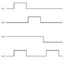
도 5는 도 4의 터치 검출 장치의 동작을 설명하기 위한 파형도이다. "SW1", "SW2", "SW3", "SW4"으로 표시된 파형은 각 스위치의 온/오프 상태를 나타내는 것으로, 파형도가 하이(high)인 상태에 해당 스위치가 온 상태가 되는 것으로 가정한다.5 is a waveform diagram for explaining the operation of the touch detection apparatus of FIG. The waveforms indicated by "SW1", "SW2", "SW3", and "SW4" indicate the on / off states of the respective switches. .
제1 스위치(SW1)가 온 상태일 때, 제2 스위치(SW2)는 오프 상태가 되며, 제3 스위치(SW3) 및 제4 스위치(SW4)는 온 상태가 된다. 제4 스위치(SW4)가 온 됨에 따라 포화 방지 정전용량(Cdrv.lpf) 양단 전위차가 0V가 되는 초기화가 이루어진다.When the first switch SW1 is in an on state, the second switch SW2 is turned off, and the third switch SW3 and the fourth switch SW4 are turned on. Initialization is performed in which the potential difference across the saturation preventing capacitance Cdrv.lpf becomes 0 V as the fourth switch SW4 is turned on.
제1 스위치(SW1)가 오프가 되고, 제2 스위치(SW2)가 온 상태가 되면, 연산 증폭기(OP-amp)의 제2 입력단을 통해 공급되는 기준 전압(Vref)에 의해 센서패드(410)가 충전되기 시작한다. 이 때, 제3 스위치(SW3)는 온 상태로 유지되며, 제4 스위치(SW4)는 오프 상태로 전환된다.When the first switch SW1 is turned off and the second switch SW2 is turned on, the reference voltage Vref supplied through the second input terminal of the operational amplifier OP- Starts charging. At this time, the third switch SW3 is kept in the ON state and the fourth switch SW4 is turned OFF.
제3 스위치(SW3)가 온 상태로 유지되기 때문에, 구동 정전용량(Cdrv)과 포화 방지 정전용량(Cdrv.lpf)은 병렬로 연결된다. 즉, 연산 증폭기(OP-amp)의 제1 입력단(N1)과 출력단(N3) 사이에 연결된 피드백 정전용량은 구동 정전용량(Cdrv)과 포화 방지 정전용량(Cdrv.lpf)이 더해진 값과 같게 된다.Since the third switch SW3 is kept in the ON state, the driving capacitance Cdrv and the saturation preventing capacitance Cdrv.lpf are connected in parallel. That is, the feedback capacitance connected between the first input terminal N1 and the output terminal N3 of the operational amplifier OP-amp becomes equal to the value obtained by adding the driving capacitance Cdrv and the saturation preventing capacitance Cdrv.lpf .
이에 따라, 센서패드(410)에의 터치 발생 전후 연산 증폭기(OP-amp) 출력 전압 변화량은 위에서 설명한 수학식 3과 같아진다.Accordingly, the amount of change in the output voltage of the operational amplifier OP-amp before and after the generation of the touch to the
전술한 바와 같이, 포화 방지 정전용량(Cdrv.lpf)이 더해짐에 따라 충전 동작 시 정전용량에 대한 포화는 방지될 수 있지만, 연산 증폭기(OP-amp) 출력 전압 변화량이 작아지게 되어 민감도는 악화될 수 있다.As described above, as the saturation prevention capacitance Cdrv.lpf is added, the saturation of the capacitance during the charging operation can be prevented, but the amount of change in the output voltage of the operational amplifier OP-amp becomes small and the sensitivity deteriorates .
따라서, 구동 정전용량(Cdrv)이 포화되지 않는 범위 내에서, 포화 방지 정전용량(Cdrv.lpf)에 충전된 전하를 구동 정전용량(Cdrv)으로 옮겨 놓을 수 있다면 민감도가 악화되지 않으면서도 포화가 방지되는 효과를 얻게 된다.Therefore, if the charge charged in the saturation preventing capacitance Cdrv.lpf can be transferred to the drive capacitance Cdrv within the range in which the drive capacitance Cdrv does not saturate, the saturation can be prevented without deteriorating the sensitivity .
다시 도 5를 참조하면, 제2 스위치(SW2)가 온 상태로 전환되고 정상 상태에 도달한 후에는 제2 스위치(SW2)가 오프 상태로 전환된다. 이 때, 제3 스위치(SW3)를 오프 상태로 전환하면, 구동 정전용량(Cdrv)의 일단(N3)과 포화 방지 정전용량(Cdrv.lpf)의 일단(N4) 간 연결이 끊어지게 되며, 이들은 직렬 연결 상태가 된다. 또한, 동시에 제4 스위치(SW4)를 온 상태로 전환하면, 포화 방지 정전용량(Cdrv.lpf)의 양단이 동전위가 되어 포화 방지 정전용량(Cdrv.lpf)에 충전되었던 전하들이 구동 정전용량(Cdrv)으로 이동하게 된다. 이는 연산 증폭기(OP-amp)의 입력이 무한대 임피던스 또는 이와 유사한 임피던스를 가지기 때문에 이동 경로가 구동 정전용량(Cdrv)을 향하는 방향밖에 없기 때문이다. 전하의 이동 방향은 포화 방지 정전용량(Cdrv.lpf) 양단의 전압이 감소하는 방향의 이동이므로 구동 정전용량(Cdrv)에는 포화 방지 정전용량(Cdrv.lpf)에 저장되었던 전하가 추가되는 결과가 된다. 구동 정전용량(Cdrv)의 일단은 기준 전압으로 유지되는 연산 증폭기(OP-amp)의 제1 입력단(N1)과 연결되어 있으므로, 연산 증폭기(OP-amp)의 출력단(N3) 전압은 포화 방지 정전용량(Cdrv.lpf)에 저장되었던 전하량의 크기에 비례하여 상승하게 된다.Referring again to FIG. 5, after the second switch SW2 is turned on and the steady state is reached, the second switch SW2 is turned off. At this time, when the third switch SW3 is turned off, the connection between one end N3 of the drive electrostatic capacitance Cdrv and one end N4 of the anti-saturation electrostatic capacitance Cdrv.lpf is cut off, Serial connection is established. At the same time, when the fourth switch SW4 is turned on, both ends of the saturation preventing capacitance Cdrv.lpf become above the electric potential and the charges charged in the saturation preventing capacitance Cdrv.lpf become the driving electrostatic capacitance Cdrv). This is because the input of the operational amplifier OP-amp has an infinite impedance or an impedance similar to that of the operational amplifier OP-amp, and thus the traveling path is only in the direction toward the driving capacitance Cdrv. Since the movement direction of the charge is the movement in the direction in which the voltage across the saturation prevention capacitance Cdrv.lpf decreases, the result is that the charge stored in the saturation prevention capacitance Cdrv.lpf is added to the driving capacitance Cdrv . Since the output terminal N3 of the operational amplifier OP-amp is connected to the first input terminal N1 of the operational amplifier OP-amp which is held at the reference voltage at one end of the driving electrostatic capacitance Cdrv, And increases in proportion to the amount of charge stored in the capacity (Cdrv.lpf).
전하 이동 전과 후의 총 전하량은 동일하므로, 다음과 같은 수학식 전개가 가능해진다.Since the total charge amount before and after the charge transfer is the same, the following expression expansion is possible.


즉, 포화 방지 정전용량(Cdrv.lpf)으로부터 구동 정전용량(Cdrv)으로 전하를 이동시킨 후의 연산 증폭기(OP-amp) 출력단(N3) 전압 변화량(ΔVafter)은 상기의 수학식에서와 같이 증가하게 되며, 처음부터 구동 정전용량(Cdrv)만으로 연산 증폭기(OP-amp) 피드백 회로를 구성한 것과 동일한 수준의 민감도를 유지할 수 있게 된다.That is, the voltage change amount? Vafter of the operational amplifier (OP-amp) output terminal N3 after the charge is moved from the saturation preventing capacitance Cdrv.lpf to the driving electrostatic capacitance Cdrv increases as shown in the above equation , It is possible to maintain the same level of sensitivity as that of the operational amplifier (OP-amp) feedback circuit formed from the beginning only by the driving capacitance Cdrv.
도 6은 본 발명의 다른 실시예에 따른 터치 검출 장치를 예시하는 회로도이다.6 is a circuit diagram illustrating a touch detection apparatus according to another embodiment of the present invention.
도 6을 참조하면, 도 4를 참조하여 설명한 회로도에 기준 전압 변화부(700)가 추가되었다는 것을 알 수 있다.Referring to FIG. 6, it can be seen that the reference
기준 전압 변화부(700)는 연산 증폭기(OP-amp)의 제2 입력단(N5)에 연결되며, 인가되는 기준 전압의 전위를 일정 구간동안 상승시키기 위한 구성요소이다.The reference
기준 전압 변화부(700)는 기준 전압 인가단(Vref)과 초과 전압 인가단(Vref.od)을 포함한다. 초과 전압 인가단(Vref.od)은 기준 전압(Vref)보다 큰 전압을 인가하는 부분이다. 또한, 기준 전압 인가단(Vref)과 초과 전압 인가단(Vref.od) 중 하나를 연산 증폭기(OP-amp)의 제2 입력단(N5)과 연결하는 제5 스위치(SW5)를 포함한다.The reference
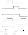
도 7은 도 6에 도시된 회로의 동작을 설명하기 위한 파형도이다. 도 7을 참조하여, 도 6의 회로도 동작을 설명하면 다음과 같다. "SW1", "SW2", "SW3", "SW4", "SW5"로 표시된 파형은 각 스위치의 온/오프 상태를 나타내는 것으로, 파형도가 하이(high)인 상태에 해당 스위치가 온 상태가 되는 것으로 가정한다. 또한, 제5 스위치(SW5)는 "SW5"의 파형도가 로우(low)일 때 초과 전압 인가단(Vref.od)과 연결되고, "SW5"의 파형도가 하이(high)일 때 기준 전압 인가단(Vref)과 연결되는 것으로 가정한다. 또한, 모니터링 전압(Vmonitor)은 제2 스위치(SW2)와 저항(Rserial)이 연결되는 노드(NM)의 전압이다.7 is a waveform diagram for explaining the operation of the circuit shown in Fig. Referring to FIG. 7, the operation of the circuit diagram of FIG. 6 will be described as follows. The waveforms indicated by "SW1", "SW2", "SW3", "SW4", and "SW5" indicate the on / off states of the respective switches. When the waveform is high, . The fifth switch SW5 is connected to the excess voltage applying stage Vref.od when the waveform of the switch SW5 is low and the waveform of the switch SW5 is high, And is connected to the application stage (Vref). The monitoring voltage Vmonitor is a voltage of the node NM to which the second switch SW2 and the resistor Rserial are connected.
제1 스위치(SW1)가 온, 제2 스위치(SW2)가 오프 상태일 때에는 모니터링 전압(Vmonitor)이 그라운드 전압이 된다. 그 후, 제2 스위치(SW2)가 온 상태로 전환되면, 저항(Rserial)에 전류가 흐르기 시작하며, 모니터링 전압(Vmonitor)은 초과 전압 인가단(Vref.od)의 전압을 향해 상승한다. 제5 스위치(SW5)가 초과 전압 인가단(Vref.od)과 연산 증폭기(OP-amp)의 제2 입력단(N5)을 연결하고 있기 때문이다. 초과 전압(Vref.od)이 기준 전압(Vref)보다 큰 값을 가지기 때문에 모니터링 전압(Vmonitor), 즉, 센서패드(410)와 저항(Rserial) 사이 노드(NM)의 전위 상승 속도가 빨라지게 된다.When the first switch SW1 is on and the second switch SW2 is off, the monitoring voltage Vmonitor becomes the ground voltage. Thereafter, when the second switch SW2 is turned on, a current starts to flow through the resistor Rserial , and the monitoring voltage Vmonitor rises toward the voltage of the excess voltage applying stage Vref.od. And the fifth switch SW5 connects the excess voltage applying stage Vref.od with the second input terminal N5 of the operational amplifier OP-amp. Since the excess voltage Vref.od has a value larger than the reference voltage Vref, the potential rise speed of the node NM between the monitoring voltage Vmonitor, that is, between the
모니터링 전압(Vmonitor)이 그라운드 전압으로부터 상승하여 기준 전압(Vref)을 넘게 되면 제5 스위치(SW5)는 기준 전압 인가단(Vref)과 연산 증폭기(OP-amp)의 제2 입력단(N5)을 연결한다. 이에 따라, 센서패드(410)와 저항(Rserial) 사이의 전위는 기준 전압(Vref)을 향해간다.When the monitoring voltage Vmonitor rises from the ground voltage and exceeds the reference voltage Vref, the fifth switch SW5 connects the reference voltage applying stage Vref and the second input terminal N5 of the operational amplifier OP-amp do. Accordingly, the potential between the
RC 회로에서의 전압값 변화는 다음의 수학식으로 나타낼 수 있는데, 이 수학식에 비추어 볼 때 기준 전압(Vref) 단일 전원만으로 센서패드(410)와 연결된 정전용량들을 충전하는 것보다, 기준 전압(Vref)보다 큰 값을 갖는 초과 전압(Vref.od)으로 초기 충전을 하는 경우가 충전 속도를 더 빠르게 할 수 있는 것이다. 즉, 초기에 초과 전압(Vref.od)으로 구동하는 것이 센서패드(410) 출력단 전압을 더욱 빨리 기준 전압(Vref)으로 끌어올릴 수 있다.The change in the voltage value in the RC circuit can be expressed by the following equation. In view of this equation, the reference voltage (Vref) The charging speed can be made faster when the initial charging is performed with the excess voltage Vref.od having a value larger than Vref. That is, it is possible to increase the output terminal voltage of the

제5 스위치(SW5)가 기준 전압 인가단(Vref)을 연산 증폭기(OP-amp)의 제2 입력단(N5)과 연결시킨 이후 정상 상태가 되면, 연산 증폭기(OP-amp)의 출력단 전압을 검출하여 터치 여부 검출을 할 수 있으며, 도 7에서는 그 시점을 화살표로 나타내었다.When the fifth switch SW5 becomes a normal state after connecting the reference voltage supply terminal Vref to the second input terminal N5 of the operational amplifier OP-amp, the output terminal voltage of the operational amplifier OP-amp is detected So that the touch can be detected. In FIG. 7, the point of time is indicated by an arrow.
모니터링 전압(Vmonitor)이 기준 전압(Vref)을 넘기만 하면 초과 전압(Vref.od)까지 도달하지 않더라도 제5 스위치(SW5)는 전환될 수 있다. 이를 위해 제5 스위치(SW5)의 동작 제어를 위한 비교기(710)가 더 추가될 수 있다.The fifth switch SW5 can be switched even if the monitoring voltage Vmonitor does not reach the excess voltage Vref.od as long as the monitoring voltage Vmonitor exceeds the reference voltage Vref. To this end, a
비교기(710)의 두 입력단에는 센서패드(710)와 저항(Rserial) 사이의 노드 전압인 모니터링 전압(Vmonitor)과 기준 전압(Vref)이 입력되고, 비교기(710)의 출력 전압은 제5 스위치(SW5)의 제어 신호로서 사용된다.A monitoring voltage Vmonitor and a reference voltage Vref which are node voltages between the
비교기(710)는 모니터링 전압(Vmonitor)이 기준 전압(Vref)보다 작을 때에는 제1 전압을 출력하고, 모니터링 전압(Vmonitor)이 기준 전압(Vref) 이상일 때에는 제2 전압을 출력한다.The
제1 전압과 제2 전압은 제5 스위치(SW5)의 제어 신호로서 이용되는데, 제1 전압은 제5 스위치(SW5)가 초과 전압 인가단(Vref.od)을 연산 증폭기(OP-amp)의 제2 입력단(N5)과 연결시키도록 제어한다. 한편, 제2 전압은 제5 스위치(SW5)가 기준 전압 인가단(Vref)을 연산 증폭기(OP-amp)의 제2 입력단(N5)과 연결시키도록 제어한다.The first voltage and the second voltage are used as a control signal of the fifth switch SW5. The first voltage is a voltage that the fifth switch SW5 supplies to the operational amplifier OP-amp To the second input terminal N5. On the other hand, the second voltage controls the fifth switch SW5 to connect the reference voltage supply terminal Vref to the second input terminal N5 of the operational amplifier OP-amp.
제5 스위치(SW5)가 초과 전압 인가단(Vref.od)과 연결될 시에, 모니터링 전압(Vmonitor)은 초과 전압(Vref.od)을 향해 증가하는데, 모니터링 전압(Vmonitor)이 기준 전압(Vref) 혹은 기준 전압(Vref)을 기준으로 일정 범위 내의 전압이 되는 순간 비교기(710)의 출력은 제2 전압으로 바뀌고, 이에 따라 제5 스위치(SW5)는 기준 전압 인가단(Vref)과 연결된다. 이에 따라, 모니터링 전압(Vmonitor), 즉, 센서패드(410)와 저항(Rserial) 사이 노드(NM)의 전압은 기준 전압(Vref)으로 유지된다. 도 7에서는 전하 이동 후 터치 여부 검출이 되는 시점을 화살표로 표시하였다.The monitoring voltage Vmonitor increases toward the excess voltage Vref.od when the fifth switch SW5 is connected to the excess voltage applying stage Vref.od and the monitoring voltage Vmonitor becomes higher than the reference voltage Vref, The output of the
실제로는 모니터링 전압(Vmonitor)의 기준 전압(Vref) 부근에서 리플(ripple)이 관측될 수 있으며, 이러한 경우 비교기(710)의 출력 전압도 달라질 수 있다. 이러한 변동을 방지하기 위해 비교기(710) 출력단에 슈미트 트리거(Schmitt trigger)를 부가하거나, 비교기(710)의 첫번째 상승 트리거만 제3 스위치(SW3)의 동작에 이용되도록 논리 회로를 부가하는 방법 등을 이용할 수 있다.A ripple can be actually observed in the vicinity of the reference voltage Vref of the monitoring voltage Vmonitor and in this case the output voltage of the
도 6을 참조하여 설명한 실시예에 따르면, 제2 스위치(SW2)가 온 상태로 전환됨과 동시에 연산 증폭기(OP-amp)의 제1 입력단(N1)을 기준 전압(Vref)보다 더 큰 초과 전압(Vref.od)으로 설정해 주기 때문에, 제2 스위치(SW2)와 저항(Rserial)을 사이에 두고 연산 증폭기(OP-amp)의 제1 입력단(N1)과 연결되는 센서패드(410)의 출력단(N2)의 전위가 그라운드 전위로부터 기준 전위(Vref)로 신속하게 상승할 수 있게 된다.6, the second switch SW2 is turned on, and at the same time the first input terminal N1 of the operational amplifier OP-amp is switched to an excess voltage (Vref) larger than the reference voltage Vref The output terminal of the
전술한 바와 같이, 터치 여부 검출은 제2 스위치(SW2)가 온 상태가 된 후 센서패드(410) 출력단(N2) 전위가 기준 전압(Vref)으로 유지되는 정상 상태에서 이루어지는데, 상기 설명한 바와 같은 이유로 정상 상태로의 도달 시간이 빨라짐에 따라 터치 여부 검출의 응답 시간을 단축시킬 수 있다.As described above, touch detection is performed in a steady state in which the potential at the output terminal N2 of the
또한, 비교기(710)의 동작에 의해 일정 조건 하에서 제5 스위치(SW5)가 동작하여 연산 증폭기(OP-amp)의 제2 입력단(N5)에 인가되는 신호가 초과 전압(Vref.od)에서 기준 전압(Vref)으로 자동 전환되므로, 제5 스위치(SW5)의 전환 시점을 미리 예측할 필요가 없게 되며, 연산 증폭기(OP-amp)의 제2 입력단(N5)에 초과 전압(Vref.od)을 필요 이상의 시간 동안 공급함으로써 발생할 수 있는 오버슈팅(over-shooting) 현상이 방지될 수 있다.The fifth switch SW5 is operated under a certain condition by the operation of the
도 8은 본 발명의 다른 실시예에 따른 터치 검출 장치를 나타내는 회로도이다.8 is a circuit diagram showing a touch detection apparatus according to another embodiment of the present invention.
도 8을 참조하면, 도 6의 회로도에 기생 정전용량 보상 회로(800) 및 기생 정전용량 제거 회로(900)가 더 포함되었다는 것을 알 수 있다.Referring to FIG. 8, it can be seen that the circuit diagram of FIG. 6 further includes a parasitic
기생 정전용량 보상 회로(800)는 피드백 정전용량(Cfb)을 포함하며, 피드백 정전용량(Cfb) 양단의 전위차는 제1 스위치(SW1)에 의해 제어된다. 피드백 정전용량(Cfb)의 일단(Nfb)은 제2 스위치(SW2)에 의해 현재 터치 여부 검출 대상인 센서패드(410-1) 출력단(N2)과 연결 또는 차단되며, 타단에는 피드백 전압(Vfb)이 인가된다.The parasitic
한편, 이하의 설명에서 기생 정전용량(Cp)은 현재 터치 여부 검출 대상이 되는 센서패드(410-1) 외의 다른 센서패드(410-2)에 의해 형성되는 기생 정전용량(Cp0), 및 터치 여부 검출 대상이 되는 센서패드(410-1)와 이웃하는 센서패드(410-2) 간의 관계에 의해 형성되는 기생 정전용량(Cpt)을 모두 합성한 개념으로 이해되어야 한다.In the following description, the parasitic capacitance Cp is expressed by the parasitic capacitance Cp0 formed by the sensor pad 410-2 other than the sensor pad 410-1, And the parasitic capacitance Cpt formed by the relationship between the sensor pad 410-1 to be detected and the neighboring sensor pad 410-2.
제1 스위치(SW1)가 온 되고 제2 스위치(SW2)가 오프 상태인 경우에는, 터치 정전용량(Ct)과 기생 정전용량(Cp) 양단의 전위차가 0V가 되어, 전하가 충전되지 않게 된다. 또한, 구동 정전용량(Cdrv) 양단위 전위차 및 피드백 정전용량(Cfb) 양단의 전위차도 0V이 되며, 제4 스위치(SW4)도 온 되어 포화 방지 정전용량(Cdrv.lpf) 양단의 전위차도 0V가 된다. 즉, 모든 정전용량에 전하가 충전되지 않게 된다. 이 때, 제5 스위치(SW5)는 초과 전압 인가단(Vref.od)과 연결되기 때문에 구동 정전용량(Cdrv) 양단의 전위는 모두 초과 전압(Vref.od)과 같아지고, 피드백 정전용량(Cfb)의 양단 전위는 모두 피드백 전압(Vfb)과 같아진다.When the first switch SW1 is turned on and the second switch SW2 is turned off, the potential difference between the touch capacitance Ct and the parasitic capacitance Cp becomes 0 V, and the charge is not charged. The potential difference between both units of the drive electrostatic capacity Cdrv and the both ends of the feedback capacitance Cfb is also 0V and the fourth switch SW4 is also turned on so that the potential difference across the saturation preventing capacitance Cdrv.lpf is 0V do. That is, no charge is charged in all the electrostatic capacitances. At this time, since the fifth switch SW5 is connected to the excess voltage applying stage Vref.od, the potentials across the driving capacitance Cdrv become equal to the excess voltage Vref.od and the feedback capacitances Cfb Is equal to the feedback voltage Vfb.
제1 스위치(SW1)가 오프, 제2 스위치(SW2)가 온, 제4 스위치(SW4)가 오프 상태가 되면, 센서패드(410-1) 출력과 저항(Rserial)이 연결되는 노드(NM)의 전위, 즉, 모니터링 전압(Vmonitor)이 초과 전압(Vref.od)을 향해 상승하게 된다. 모니터링 전압(Vmonitor)이 초과 전압(Vref.od) 부근에 도달하면, 제5 스위치(SW5)가 기준 전압 인가단(Vref)과 연결되고 모니터링 전압(Vmonitor)은 기준 전압(Vref)으로 유지된다.A first switch (SW1) is turned off, the second switch (SW2) is turned on, when the fourth switch is turned off (SW4), the sensor pad (410-1) and an output resistance (Rserial) node (NM which is connected , That is, the monitoring voltage Vmonitor rises toward the excess voltage Vref.od. When the monitoring voltage Vmonitor reaches about the excess voltage Vref.od, the fifth switch SW5 is connected to the reference voltage supply terminal Vref and the monitoring voltage Vmonitor is maintained at the reference voltage Vref.
이에 따라, 터치 정전용량(Ct)과 기생 정전용량(Cp)이 모두 기준 전압(Vref)에 의해 충전된다.Thus, both the touch capacitance Ct and the parasitic capacitance Cp are charged by the reference voltage Vref.
한편, 피드백 전압(Vfb)이 기준 전압(Vref)보다 크다면, 피드백 정전용량(Cfb) 양단 간에는 전위차가 발생하게 된다. 구체적으로, 피드백 정전용량(Cfb)의 양단 중 센서패드(410-1)의 출력과 연결되는 일단(Nfb)의 전위가 피드백 전압(Vfb)이 인가되는 타단보다 낮은 전위가 되며, 이에 따라 피드백 정전용량(Cfb)은 터치 검출 장치에 전하를 공급하는 역할을 하게 된다.On the other hand, if the feedback voltage Vfb is larger than the reference voltage Vref, a potential difference is generated across the feedback capacitance Cfb. Specifically, the potential of one end Nfb connected to the output of the sensor pad 410-1 at both ends of the feedback capacitance Cfb becomes lower than the potential at the other end to which the feedback voltage Vfb is applied, The capacitance Cfb serves to supply electric charge to the touch detection device.
정상 상태에서 터치 정전용량(Ct) 및 기생 정전용량(Cp)에 충전된 전하량의 합(Q1)은 구동 정전용량(Cdrv)과 포화 방지 정전용량(Cdrv.lpf) 및 피드백 정전용량(Cfb)이 공급하는 전하량의 합(Q2)과 같아지므로 다음과 같은 수학식이 전개될 수 있다.The sum (Q1) of the charge amount on the touch capacitance (Ct) and the parasitic capacitance (Cp) in the steady state is the driving capacitance (Cdrv) to prevent saturation capacitance (Cdrv.lpf) and feedback capacitance (Cfb) Is equal to the sum (Q2 ) of the amounts of supplied charges, the following equation can be developed.


여기서, 피드백 전압(Vfb)을 기준 전압(Vref)의 2배인 것으로 가정하고, 이를 대입하면, 다음과 같아진다.Here, it is assumed that the feedback voltage Vfb is twice the reference voltage Vref, and substituting it is as follows.

한편, 터치 전후 연산 증폭기(OP-amp)의 출력단(N3) 전압의 변화량, 즉, 레벨 시프트(ΔVo) 값은 구동 정전용량(Cdrv) 양단의 전압(Vdrv)과 같은 값이 되기 때문에, 수학식 7에서 Vdrv를 ΔVo로 치환하면 다음과 같아진다.On the other hand, since the amount of change in the voltage at the output terminal N3 of the pre-touch operational amplifier OP-amp, that is, the level shift? Va becomes the same value as the voltage Vdrv across the drive capacitance Cdrv, 7, Vdrv is replaced by ΔVo.

이 때, 구동 정전용량(Cdrv)이 포화가 되지 않았다면, 제2 스위치(SW2)를 오프 시킨 상태에서 제3 스위치(SW3)를 오프 상태로 전환하고, 제4 스위치(SW4)를 온 상태로 전환시켜 포화 방지 정전용량(Cdrv.lpf)에 저장되었던 전하를 구동 정전용량(Cdrv)으로 이동시킨다. 이는 도 4 및 도 5를 참조하여 설명하였던 바와 같이, 포화를 방지하면서도 민감도를 악화시키지 않기 위한 것이다.At this time, if the drive capacitance Cdrv is not saturated, the third switch SW3 is switched to the off state while the second switch SW2 is turned off, and the fourth switch SW4 is switched to the on state Thereby transferring the charge stored in the saturation prevention capacitance Cdrv.lpf to the driving capacitance Cdrv. This is to prevent saturation and deteriorate the sensitivity as described with reference to Figs. 4 and 5. Fig.
전하 이동 전과 후의 관계에 관한 수학식 4를 수학식 8에 대입하면, 다음과 같은 최종 레벨 시프트 값이 도출될 수 있다.Substituting Equation (4) for the relationship before and after the charge transfer into Equation (8), the following final level shift value can be derived.

즉, 최종적으로 도출되는 레벨 시프트 값은 처음부터 구동 정전용량(Cdrv)만으로 연산 증폭기(OP-amp)의 피드백 회로를 구성한 경우와 동일한 민감도를 가질 수 있게 된다.That is, the finally obtained level shift value can have the same sensitivity as that in the case of constituting the feedback circuit of the operational amplifier OP-amp from the beginning only by the driving capacitance Cdrv.
한편, 상기 수학식 9에서 피드백 정전용량(Cfb)을 기생 정전용량(Cp)과 동일한 값으로 조절할 수 있다면, 터치 전후의 레벨 시프트(ΔVo) 값은 기생 정전용량(Cp)에 무관한 값이 될 수 있다.If the feedback capacitance Cfb can be adjusted to the same value as the parasitic capacitance Cp in the above Equation 9, the value of the level shift? Vo before and after the touch becomes a value independent of the parasitic capacitance Cp .
즉, 제2 스위치(SW2)가 온 상태일 때 기생 정전용량 보상 회로(800)로부터 일정량의 전하량이 공급되는데, 피드백 정전용량(Cfb)의 크기를 적절히 조절한다면, 기생 정전용량 보상 회로(800)가 터치 정전용량(Ct) 외의 다른 모든 기생 정전용량(Cp)을 충전시키는 역할을 하게 된다. 따라서, 구동 정전용량(Cdrv)에 의한 충전이 터치 정전용량(Ct)만을 충전시키게 되므로, 터치 전후의 레벨 시프트(ΔVo) 값은 기생 정전용량(Cp)과 무관하며 터치 정전용량(Ct)에만 관계있는 값이 된다.That is, when the second switch SW2 is turned on, a certain amount of charge is supplied from the parasitic
피드백 정전용량(Cfb)의 크기를 최적화하는 과정을 설명하면 다음과 같다. 터치 정전용량(Ct)을 '0'이라 가정할 경우, 기생 정전용량(Cp)이 완전히 제거된다면, 제1 스위치(SW1)와 제4 스위치(SW4), 및 제2 스위치(SW2)가 번갈아 온/오프 되는 과정을 거쳤을 때, 연산 증폭기(OP-amp) 출력단 전압은 기준 전압(Vref)이 되어야 한다. 왜냐하면, 이상적인 경우 터치 검출 장치에 충전된 전하량의 변화가 없어야 하며, 이 때 연산 증폭기(OP-amp)의 제1 입력단과 출력단 간의 전위차는 언제나 '0'이어야 하기 때문이다.A process of optimizing the magnitude of the feedback capacitance (Cfb) will be described below. Assuming that the touch capacitance Ct is '0', if the parasitic capacitance Cp is completely removed, the first switch SW1, the fourth switch SW4, and the second switch SW2 are alternately turned on / Off, the output voltage of the operational amplifier (OP-amp) should be the reference voltage (Vref). This is because, in an ideal case, there should be no change in the amount of charge charged in the touch detection apparatus, and the potential difference between the first input terminal and the output terminal of the operational amplifier OP-amp must always be '0'.
따라서, 피드백 정전용량(Cfb) 값을 변화시키면서 연산 증폭기(OP-amp)의 출력단 전압 또는 아날로그-디지털 변환기(ADC)의 출력단 전압을 확인한다면, 최적의 피드백 정전용량(Cfb) 값을 택할 수 있게 된다. 다른 소자의 파라미터, 예를 들면, 구동 정전용량(Cdrv) 값과 상관없이 피드백 정전용량(Cfb) 값만을 변화시키면서 최적의 값을 찾을 수 있으므로, 간단한 회로 교정 또는 최적화가 가능해진다.Therefore, if the output terminal voltage of the operational amplifier OP-amp or the output terminal voltage of the analog-digital converter ADC is checked while changing the feedback capacitance Cfb, the optimum feedback capacitance Cfb can be selected do. An optimum value can be found while changing only the feedback capacitance Cfb regardless of the parameter of another element, for example, the driving capacitance Cdrv, so that simple circuit calibration or optimization becomes possible.
한편, 기생 정전용량 제거 회로(900)는 터치 검출 대상이 되는 센서패드(410-1)와 인접한 다른 센서패드(410-2) 간의 관계에 의해 형성되는 기생 정전용량(Cpt)을 최소화하는 기능을 한다.On the other hand, the parasitic
이러한 기능 수행을 위해 기생 정전용량 제거 회로(900)는 현재 터치 여부 검출 대상이 되는 센서패드(410-1)의 출력단 전압과 동일한 전압을 다른 센서패드(410-2)에 공급한다.In order to perform such a function, the parasitic
제1 스위치(SW1)가 온 상태일 때에는 현재 터치 검출 대상이 되는 센서패드(410-1)의 출력이 그라운드와 연결된다. 따라서, 센서패드(410-1)의 출력단(N2) 전위는 그라운드 전압(GND)과 같아진다.When the first switch SW1 is on, the output of the sensor pad 410-1, which is the current touch detection object, is connected to the ground. Therefore, the potential at the output terminal N2 of the sensor pad 410-1 becomes equal to the ground voltage GND.
한편, 제2 스위치(SW2)가 온 상태일 때에는 현재 터치 검출 대상이 되는 센서패드(410-1)의 출력이 연산 증폭기(OP-amp)의 제1 입력단과 연결된다. 연산 증폭기(OP-amp)의 제2 입력단에는 기준 전압(Vref)이 공급되고 있으므로, 센서패드(410-1)의 출력단(N2) 전위 또한 기준 전압(Vref)과 같아진다.On the other hand, when the second switch SW2 is on, the output of the sensor pad 410-1, which is the current touch detection object, is connected to the first input terminal of the operational amplifier OP-amp. Since the reference voltage Vref is supplied to the second input terminal of the operational amplifier OP-amp, the potential at the output terminal N2 of the sensor pad 410-1 becomes equal to the reference voltage Vref.
따라서, 제1 스위치(SW1)가 온 상태일 때에는 터치 검출 대상이 되는 센서패드(410-1) 이외의 다른 센서패드(410-2)에 그라운드 전위(GND)를 공급해주고, 제2 스위치(SW2)가 온 상태일 때에는 터치 검출 대상이 되는 센서패드(410-1) 이외의 다른 센서패드(410-2)에 기준 전압(Vref)을 공급해준다면, 인접하는 센서패드 간 전위차는 0으로 유지될 수 있다.Therefore, when the first switch SW1 is in the ON state, the ground potential GND is supplied to the sensor pad 410-2 other than the sensor pad 410-1 to be the touch detection object, and the second switch SW2 When the reference voltage Vref is supplied to the sensor pad 410-2 other than the sensor pad 410-1 to be the touch detection object, the potential difference between the adjacent sensor pads can be maintained at zero have.
사이에 유전 물질을 두고 2개의 도체가 존재한다면, 해당 구조에 충전되는 전하량(Q)은 Q=CV와 같은 수식으로 표현될 수 있다. 여기서, C는 해당 구조의 정전용량 값이며, V는 양 도체 사이의 전위차이다.If there are two conductors with a dielectric material between them, the amount of charge Q filled in the structure can be expressed as Q = CV. Where C is the capacitance value of the structure and V is the potential difference between both conductors.
상기 수식에서, 양 도체의 전위차(V)를 0에 가깝도록 수렴시키면, 도체간 전위 차에 의해 끌려지는 전하량(Q)도 0에 가깝게 수렴시킬 수 있다. 정전용량(C)은 전하의 충전 능력에 비례하는 것이므로, 충전되는 전하량(Q)이 0에 가깝게 된다면, 도체 간 관계에 의해 형성되는 정전용량(C)도 0에 가깝게 수렴한다는 의미가 된다.In the above equation, when the potential difference (V) of both conductors is converged close to zero, the amount of charge Q drawn by the inter-conductor potential difference can also converge to zero. Since the electrostatic capacitance C is proportional to the charging ability of the electric charge, if the electric charge quantity Q to be charged becomes close to 0, the electrostatic capacity C formed by the inter-conductor relation also converges to zero.
따라서, 2개의 센서패드(410-1, 410-2) 간 전위차를 항상 0에 가깝게 되도록 제어한다면, 2개의 센서패드(410-1, 410-2) 간 관계에 의해 발생할 수 있는 기생 정전용량(Cpt) 또한 최소화될 수 있다.Therefore, if the potential difference between the two sensor pads 410-1 and 410-2 is controlled to be always close to 0, the parasitic capacitance (hereinafter referred to as " parasitic capacitance " Cpt) can also be minimized.
현재 터치 검출 대상이 되는 센서패드(410-1) 이외의 센서패드(410-2)에 그라운드 전위(GND) 및 기준 전압(Vref)을 교번하여 공급하는 기생 정전용량 제거 회로(900)는 제1 입력단이 출력과 연결된 피드백 증폭기(OP-amp_fb)를 포함할 수 있다. 피드백 증폭기(OP-amp_fb)의 제2 입력단에는 그라운드 전위(GND)와 기준 전압(Vref)을 교번하여 공급하는 신호원(SS)이 연결될 수 있다.The parasitic
신호원(SS)은 로우(low) 신호가 그라운드 전위(GND)이고 하이(hing) 신호가 기준 전압(Vref)과 동일한 클록 신호일 수 있다. 신호원(SS)이 클록 신호일 때 그 주파수는 제1 스위치(SW1) 및 제2 스위치(SW2)의 스위칭 주파수와 동일하여야 하며, 제1 스위치(SW1)가 온 상태일 때에는 로우 신호, 제2 스위치(SW2)가 온 상태일 때에는 하이 신호가 출력되도록 동기화되어야 한다.The signal source SS may be a clock signal whose low signal is at the ground potential GND and whose hinging signal is equal to the reference voltage Vref. When the signal source SS is a clock signal, the frequency should be the same as the switching frequency of the first switch SW1 and the second switch SW2. When the first switch SW1 is in the ON state, (SW2) is in the ON state, a high signal should be output.
또한, 다른 예로 신호원(SS)은 기준 전압(Vref) 공급원과 스위치(미도시됨)로 구현될 수도 있다. 피드백 증폭기(OP-amp_fb)의 제2 입력단에 기준 전압(Vref)을 공급하되, 스위치를 통해 일정 간격으로 그 공급을 차단할 수 있다. 제1 스위치(SW1)가 온 될 때에는 기준 전압(Vref)의 공급을 차단하고, 제2 스위치(SW2)가 온 될 때에는 기준 전압(Vref)의 공급을 허용함으로써 신호원(SS)의 기능을 할 수 있다. 이 경우 피드백 증폭기(OP-amp_fb)의 제2 입력단과 기준 전압(Vref)을 연결 또는 차단시키는 스위치는 제2 스위치(SW2)와 동기화되어 온/오프 될 수 있다.Also, as another example, the signal source SS may be implemented with a reference voltage (Vref) source and a switch (not shown). The reference voltage Vref is supplied to the second input terminal of the feedback amplifier OP-amp_fb, and the supply of the reference voltage Vref can be interrupted at predetermined intervals through the switch. The supply of the reference voltage Vref is cut off when the first switch SW1 is turned on and the supply of the reference voltage Vref is turned on when the second switch SW2 is turned on to perform the function of the signal source SS . In this case, the switch for connecting or disconnecting the second input terminal of the feedback amplifier OP-amp_fb and the reference voltage Vref may be turned on / off in synchronization with the second switch SW2.
한편, 도 8에는 기생 정전용량 제거 회로(900)에 피드백 증폭기(OP-amp_fb)가 포함되는 것으로 예시되었으나, 피드백 증폭기(OP-amp-fb)는 제2 입력단에 공급되는 신호의 변형을 최소화하고 안정도를 향상시키기 위한 소자이므로, 피드백 증폭기(OP-amp_fb)는 생략되고, 신호원(SS)이 직접적으로 센서패드(410-2)의 출력과 연결될 수도 있음은 물론이다.8, the parasitic
전술한 본 발명의 설명은 예시를 위한 것이며, 본 발명이 속하는 기술분야의 통상의 지식을 가진 자는 본 발명의 기술적 사상이나 필수적인 특징을 변경하지 않고서 다른 구체적인 형태로 쉽게 변형이 가능하다는 것을 이해할 수 있을 것이다. 그러므로 이상에서 기술한 실시예들은 모든 면에서 예시적인 것이며 한정적이 아닌 것으로 이해해야만 한다. 예를 들어, 단일형으로 설명되어 있는 각 구성 요소는 분산되어 실시될 수도 있으며, 마찬가지로 분산된 것으로 설명되어 있는 구성 요소들도 결합된 형태로 실시될 수 있다.It will be understood by those skilled in the art that the foregoing description of the present invention is for illustrative purposes only and that those of ordinary skill in the art can readily understand that various changes and modifications may be made without departing from the spirit or essential characteristics of the present invention. will be. It is therefore to be understood that the above-described embodiments are illustrative in all aspects and not restrictive. For example, each component described as a single entity may be distributed and implemented, and components described as being distributed may also be implemented in a combined form.
본 발명의 범위는 후술하는 특허청구범위에 의하여 나타내어지며, 특허청구범위의 의미 및 범위 그리고 그 균등 개념으로부터 도출되는 모든 변경 또는 변형된 형태가 본 발명의 범위에 포함되는 것으로 해석되어야 한다.The scope of the present invention is defined by the appended claims, and all changes or modifications derived from the meaning and scope of the claims and their equivalents should be construed as being included within the scope of the present invention.
410: 센서패드
500: 구동 정전용량 포화 방지부
700: 기준 전압 변화부
710: 비교기
800: 기생 정전용량 보상 회로
900: 기생 정전용량 제거 회로410: sensor pad
500: driving capacitance saturation prevention unit
700: Reference voltage changing section
710: comparator
800: Parasitic capacitance compensation circuit
900: Parasitic capacitance elimination circuit
Claims (17)
Translated fromKorean상기 센서패드의 출력단과 연결된 제1 입력단 및 기준 전압을 수신하는 제2 입력단을 가지며, 터치 여부에 따라 서로 다른 신호를 출력하는 연산 증폭기;
상기 연산 증폭기의 제1 입력단과 출력단 사이에 연결된 구동 정전용량 양단의 전위를 제어하는 제1 스위치;
상기 센서패드의 출력단과 상기 연산 증폭기의 제1 입력단 간의 연결을 스위칭하며, 상기 제1 스위치와 교번하여 온/오프되는 제2 스위치; 및
상기 구동 정전용량에 선택적으로 정전용량을 병렬 또는 직렬로 부가하여, 상기 구동 정전용량과 전하를 공유하는 구동 정전용량 포화 방지부를 포함하는, 터치 검출 장치.A sensor pad forming a touch capacitance in relation to the touch input tool;
An operational amplifier having a first input terminal connected to the output terminal of the sensor pad and a second input terminal receiving the reference voltage,
A first switch for controlling a potential at both ends of a driving capacitance connected between a first input terminal and an output terminal of the operational amplifier;
A second switch for switching a connection between an output terminal of the sensor pad and a first input terminal of the operational amplifier and being turned on / off alternately with the first switch; And
And a driving capacitance saturation preventing unit that selectively adds a capacitance to the driving capacitance in parallel or in series to share electric charge with the driving capacitance.
상기 구동 정전용량 포화 방지부는,
포화 방지 정전용량;
상기 제2 스위치가 온 상태일 때 상기 포화 방지 정전용량을 상기 구동 정전용량과 병렬 연결시키는 제3 스위치; 및
상기 제2 스위치 및 제3 스위치가 오프 상태일 때 상기 포화 방지 정전용량 양단을 동전위로 제어하여 상기 포화 방지 정전용량의 전하가 상기 구동 정전용량으로 이동할 수 있도록 하는 제4 스위치를 포함하는, 터치 검출 장치.The method according to claim 1,
The driving capacitance saturation prevention unit may include:
Saturation-proof capacitance;
A third switch for connecting the anti-saturation capacitance with the driving capacitance in parallel when the second switch is on; And
And a fourth switch for controlling both terminals of the anti-saturation capacitance to coincide when the second switch and the third switch are in an off state so that the charge of the anti-saturation capacitance can move to the driving capacitance. Device.
상기 연산 증폭기의 제2 입력단에는 초과 전압이 인가되며, 상기 제2 스위치가 온 상태로 전환된 후 일정 시간 경과 후에는 상기 초과 전압보다 낮은 기준 전압이 인가되는, 터치 검출 장치.The method according to claim 1,
An overvoltage is applied to the second input terminal of the operational amplifier and a reference voltage lower than the excess voltage is applied after a predetermined time elapses after the second switch is turned on.
상기 연산 증폭기의 제2 입력단에 상기 초과 전압과 상기 기준 전압이 선택적으로 인가되도록 제어하는 제5 스위치를 더 포함하는, 터치 검출 장치.The method of claim 3,
And a fifth switch for selectively applying the excess voltage and the reference voltage to a second input terminal of the operational amplifier.
상기 센서패드의 출력 전압과 상기 기준 전압을 비교하여, 상기 센서패드의 출력 전압이 상기 기준 전압 이상이 될 때에는 상기 연산 증폭기의 제2 입력단에 상기 기준 전압이 인가되도록 상기 제5 스위치를 제어하는 비교기를 더 포함하는, 터치 검출 장치.5. The method of claim 4,
A comparator for comparing the output voltage of the sensor pad with the reference voltage and controlling the fifth switch to apply the reference voltage to the second input terminal of the operational amplifier when the output voltage of the sensor pad becomes equal to or greater than the reference voltage, Further comprising:
상기 제2 스위치가 온 상태일 때 상기 센서패드와 연결된 기생 정전용량 또는 상기 터치 정전용량 중 적어도 일부를 충전시키는 기생 정전용량 보상 회로를 더 포함하는, 터치 검출 장치.The method according to claim 1,
Further comprising a parasitic capacitance compensation circuit that charges at least a part of the parasitic capacitance or the touch capacitance connected to the sensor pad when the second switch is in the ON state.
상기 기생 정전용량 보상 회로는,
상기 제2 스위치가 온 상태일 때 일단이 상기 센서패드와 연결되며 타단에는 피드백 전압이 공급되는 피드백 정전용량을 포함하는, 터치 검출 장치.The method according to claim 6,
Wherein the parasitic capacitance compensation circuit comprises:
And a feedback capacitance whose one end is connected to the sensor pad and the other end is fed with a feedback voltage when the second switch is in the ON state.
상기 센서패드의 출력 전압과 동일한 전압을 다른 센서패드에 인가하는 기생 정전용량 제거 회로를 더 포함하는, 터치 검출 장치.The method according to claim 1,
Further comprising a parasitic capacitance elimination circuit for applying a voltage equal to an output voltage of the sensor pad to another sensor pad.
상기 기생 정전용량 제거 회로는,
상기 제1 스위치가 온 상태일 때에는 그라운드 전압, 상기 제2 스위치가 온 상태일 때에는 상기 기준 전압과 동일한 크기의 전압을 상기 다른 센서패드에 인가하는, 터치 검출 장치.9. The method of claim 8,
Wherein the parasitic capacitance elimination circuit comprises:
And applies a ground voltage to the other sensor pad when the first switch is in the on state and a voltage in the same magnitude as the reference voltage when the second switch is in the on state.
상기 센서패드 출력단을 상기 구동 정전용량의 일단과 연결시켜, 상기 구동 정전용량과 상기 포화 방지 정전용량이 충전될 수 있도록 하는 단계;
상기 센서패드 출력단과 상기 구동 정전용량 간의 연결을 차단하고, 상기 포화 방지 정전용량에 충전된 전하를 상기 구동 정전용량으로 이동시키는 단계; 및
상기 구동 정전용량의 타단 전압 변동분을 기초로 터치 여부를 검출하는 단계를 포함하는, 터치 검출 방법.A sensor pad for forming a touch capacitance in relation to the touch input tool, a drive capacitance for supplying a reference voltage to the one end, and a sensor pad, a drive capacitance, and the like for initializing a saturation prevention capacitance connected in parallel with the drive capacitance. Anti-saturation capacitance initialization step;
Connecting the output terminal of the sensor pad to one end of the driving electrostatic capacitance so that the driving electrostatic capacitance and the saturation preventing electrostatic capacitance can be charged;
Blocking the connection between the output terminal of the sensor pad and the driving electrostatic capacitance and moving the charge charged in the saturation preventing electrostatic capacitance to the driving electrostatic capacitance; And
Detecting whether or not the touch is detected based on the other-end voltage variation of the drive electrostatic capacitance.
상기 포화 방지 정전용량의 전하를 이동시키는 단계는,
상기 포화 방지 정전용량의 일단과 상기 구동 정전용량의 일단 간 연결을 차단하고, 상기 포화 방지 정전용량의 양단을 동전위로 제어하는 단계를 포함하는, 터치 검출 방법.11. The method of claim 10,
The step of moving charge of the saturation-
Blocking a connection between one end of the saturation-preventing capacitance and one end of the driving capacitance, and controlling both ends of the anti-saturation capacitance to a coincidence.
상기 포화 방지 정전용량과 구동 정전용량의 충전 단계는,
상기 구동 정전용량 일단에 초과 전압 및 상기 초과 전압보다 낮은 기준 전압 중 어느 하나를 인가하는 단계를 포함하는, 터치 검출 방법.11. The method of claim 10,
The charging step of the saturation preventing capacitance and the driving electrostatic capacitance includes:
Applying either one of an overvoltage and a reference voltage lower than the overvoltage to the one end of the driving capacitance.
상기 포화 방지 정전용량과 구동 정전용량의 충전 단계는,
상기 센서패드의 출력 전압과 상기 기준 전압을 비교하여, 상기 센서패드의 출력 전압이 상기 기준 전압 이상이 될 때 상기 기준 전압을 인가하는 단계를 포함하는, 터치 검출 방법.13. The method of claim 12,
The charging step of the saturation preventing capacitance and the driving electrostatic capacitance includes:
And comparing the output voltage of the sensor pad with the reference voltage to apply the reference voltage when an output voltage of the sensor pad becomes equal to or higher than the reference voltage.
상기 포화 방지 정전용량과 구동 정전용량의 충전 단계는,
기생 정전용량 보상 회로를 통해 상기 센서패드와 연결된 기생 정전용량 또는 상기 터치 정전용량 중 적어도 일부를 충전시키는 단계를 포함하는, 터치 검출 방법.11. The method of claim 10,
The charging step of the saturation preventing capacitance and the driving electrostatic capacitance includes:
And charging at least a portion of the parasitic capacitance or the touch capacitance connected to the sensor pad via a parasitic capacitance compensation circuit.
상기 기생 정전용량 보상 회로는,
일단이 상기 센서패드와 연결되며 타단에 피드백 전압이 공급되는 피드백 정전용량을 통해 충전을 수행하는, 터치 검출 방법.15. The method of claim 14,
Wherein the parasitic capacitance compensation circuit comprises:
Wherein the charging is performed through a feedback capacitance whose one end is connected to the sensor pad and a feedback voltage is supplied to the other end.
상기 초기화 단계는, 상기 센서패드 외의 다른 센서패드에 그라운드 전압을 인가하는 단계를 포함하고,
상기 충전 단계는, 상기 다른 센서패드에 상기 기준 전압을 인가하는 단계를 포함하는, 터치 검출 방법.11. The method of claim 10,
Wherein the initializing step includes applying a ground voltage to a sensor pad other than the sensor pad,
Wherein the charging step comprises applying the reference voltage to the other sensor pad.
상기 센서패드에의 터치 여부에 따라 서로 다른 신호를 출력하며, 제1 입력단이 상기 센서패드와 교번하여 연결 및 차단되는 연산 증폭기;
상기 연산 증폭기의 제1 입력단과 출력단 사이에 연결된 구동 정전용량; 및
상기 구동 정전용량에 선택적으로 정전용량을 병렬 또는 직렬로 부가하는 구동 정전용량 포화 방지부를 포함하는, 터치 검출 장치.A sensor pad forming a touch capacitance in relation to the touch input tool;
An operational amplifier for outputting different signals depending on whether the sensor pad is touched or not and having a first input terminal connected to and disconnected from the sensor pad;
A driving electrostatic capacitance connected between the first input terminal and the output terminal of the operational amplifier; And
And a driving capacitance saturation preventing portion that selectively adds the capacitance to the driving capacitance in parallel or in series.
Priority Applications (1)
| Application Number | Priority Date | Filing Date | Title |
|---|---|---|---|
| KR1020140063176AKR101569337B1 (en) | 2014-05-26 | 2014-05-26 | Touch detecting apparatus and method |
Applications Claiming Priority (1)
| Application Number | Priority Date | Filing Date | Title |
|---|---|---|---|
| KR1020140063176AKR101569337B1 (en) | 2014-05-26 | 2014-05-26 | Touch detecting apparatus and method |
Publications (1)
| Publication Number | Publication Date |
|---|---|
| KR101569337B1true KR101569337B1 (en) | 2015-11-16 |
Family
ID=54785888
Family Applications (1)
| Application Number | Title | Priority Date | Filing Date |
|---|---|---|---|
| KR1020140063176AExpired - Fee RelatedKR101569337B1 (en) | 2014-05-26 | 2014-05-26 | Touch detecting apparatus and method |
Country Status (1)
| Country | Link |
|---|---|
| KR (1) | KR101569337B1 (en) |
Cited By (3)
| Publication number | Priority date | Publication date | Assignee | Title |
|---|---|---|---|---|
| KR20170081091A (en)* | 2015-12-31 | 2017-07-11 | 엘지디스플레이 주식회사 | Display Device Having Touch Sensor |
| CN109407873A (en)* | 2017-08-17 | 2019-03-01 | 深圳指芯智能科技有限公司 | The detection circuit of low-power consumption touch sensible, device and method |
| WO2024192958A1 (en)* | 2023-03-20 | 2024-09-26 | 上海海栎创科技股份有限公司 | Touch sensing system |
- 2014
- 2014-05-26KRKR1020140063176Apatent/KR101569337B1/ennot_activeExpired - Fee Related
Cited By (6)
| Publication number | Priority date | Publication date | Assignee | Title |
|---|---|---|---|---|
| KR20170081091A (en)* | 2015-12-31 | 2017-07-11 | 엘지디스플레이 주식회사 | Display Device Having Touch Sensor |
| KR102545694B1 (en)* | 2015-12-31 | 2023-06-20 | 엘지디스플레이 주식회사 | Display Device Having Touch Sensor |
| CN109407873A (en)* | 2017-08-17 | 2019-03-01 | 深圳指芯智能科技有限公司 | The detection circuit of low-power consumption touch sensible, device and method |
| CN109407873B (en)* | 2017-08-17 | 2024-06-07 | 江西指芯智能科技有限公司 | Detection circuit, device and method for low-power-consumption touch induction |
| WO2024192958A1 (en)* | 2023-03-20 | 2024-09-26 | 上海海栎创科技股份有限公司 | Touch sensing system |
| US12340053B2 (en) | 2023-03-20 | 2025-06-24 | Shanghai Hynitron Technology Co., Ltd. | Touch sensing system |
Similar Documents
| Publication | Publication Date | Title |
|---|---|---|
| KR101502904B1 (en) | Touch detecting apparatus and method for adjusting parasitic capacitance | |
| KR101473186B1 (en) | Touch detecting apparatus and method | |
| US20190012035A1 (en) | Position-Sensing and Force Detection Panel | |
| US20160378252A1 (en) | Apparatus and Method for Detecting Touch | |
| KR101537231B1 (en) | Touch detecting apparatus and method | |
| KR101444524B1 (en) | Apparatus and method for sensing capacitance, and touchscreen apparatus | |
| KR101621233B1 (en) | Touch detecting apparatus and method | |
| KR101569337B1 (en) | Touch detecting apparatus and method | |
| KR101537229B1 (en) | Touch detecting apparatus and method | |
| KR101580381B1 (en) | Apparatus for touchscreen and method for controlling thereof | |
| KR101502907B1 (en) | Touch detecting apparatus and method | |
| TWI645326B (en) | Resistive force sensing circuit and resistive force sensing apparatus | |
| KR101553604B1 (en) | Touch detecting apparatus and method | |
| KR20150093395A (en) | Apparatus and method for sensing capacitance | |
| KR101537228B1 (en) | Touch detecting apparatus and method | |
| KR20150001487A (en) | Touch detecting apparatus and method | |
| KR20170025107A (en) | Touch detecting apparatus comprising flexible touch screen and method | |
| KR101554247B1 (en) | Capacitive type touch input device with structure reducing effect from stray capacitance | |
| KR20150001489A (en) | Touch detecting apparatus and method | |
| KR101482932B1 (en) | Touch detecting apparatus | |
| KR20170025106A (en) | Touch detecting apparatus comprising flexible touch screen and method | |
| JP7245995B2 (en) | Detection circuit and load detection device | |
| KR101553605B1 (en) | Touch detecting apparatus and method | |
| KR101461929B1 (en) | Touch detecting apparatus and method using sinusoidal voltage | |
| KR102337407B1 (en) | Touch input sensing apparatus and touchscreen apparatus including the same |
Legal Events
| Date | Code | Title | Description |
|---|---|---|---|
| PA0109 | Patent application | St.27 status event code:A-0-1-A10-A12-nap-PA0109 | |
| PA0201 | Request for examination | St.27 status event code:A-1-2-D10-D11-exm-PA0201 | |
| P11-X000 | Amendment of application requested | St.27 status event code:A-2-2-P10-P11-nap-X000 | |
| P13-X000 | Application amended | St.27 status event code:A-2-2-P10-P13-nap-X000 | |
| R18-X000 | Changes to party contact information recorded | St.27 status event code:A-3-3-R10-R18-oth-X000 | |
| R18-X000 | Changes to party contact information recorded | St.27 status event code:A-3-3-R10-R18-oth-X000 | |
| D13-X000 | Search requested | St.27 status event code:A-1-2-D10-D13-srh-X000 | |
| R18-X000 | Changes to party contact information recorded | St.27 status event code:A-3-3-R10-R18-oth-X000 | |
| D14-X000 | Search report completed | St.27 status event code:A-1-2-D10-D14-srh-X000 | |
| PE0902 | Notice of grounds for rejection | St.27 status event code:A-1-2-D10-D21-exm-PE0902 | |
| P11-X000 | Amendment of application requested | St.27 status event code:A-2-2-P10-P11-nap-X000 | |
| P13-X000 | Application amended | St.27 status event code:A-2-2-P10-P13-nap-X000 | |
| E701 | Decision to grant or registration of patent right | ||
| PE0701 | Decision of registration | St.27 status event code:A-1-2-D10-D22-exm-PE0701 | |
| GRNT | Written decision to grant | ||
| PR0701 | Registration of establishment | St.27 status event code:A-2-4-F10-F11-exm-PR0701 | |
| PR1002 | Payment of registration fee | St.27 status event code:A-2-2-U10-U11-oth-PR1002 Fee payment year number:1 | |
| PG1601 | Publication of registration | St.27 status event code:A-4-4-Q10-Q13-nap-PG1601 | |
| R18-X000 | Changes to party contact information recorded | St.27 status event code:A-5-5-R10-R18-oth-X000 | |
| P22-X000 | Classification modified | St.27 status event code:A-4-4-P10-P22-nap-X000 | |
| PN2301 | Change of applicant | St.27 status event code:A-5-5-R10-R13-asn-PN2301 St.27 status event code:A-5-5-R10-R11-asn-PN2301 | |
| PR1001 | Payment of annual fee | St.27 status event code:A-4-4-U10-U11-oth-PR1001 Fee payment year number:4 | |
| P22-X000 | Classification modified | St.27 status event code:A-4-4-P10-P22-nap-X000 | |
| FPAY | Annual fee payment | Payment date:20190909 Year of fee payment:5 | |
| PR1001 | Payment of annual fee | St.27 status event code:A-4-4-U10-U11-oth-PR1001 Fee payment year number:5 | |
| PC1903 | Unpaid annual fee | St.27 status event code:A-4-4-U10-U13-oth-PC1903 Not in force date:20201111 Payment event data comment text:Termination Category : DEFAULT_OF_REGISTRATION_FEE | |
| P22-X000 | Classification modified | St.27 status event code:A-4-4-P10-P22-nap-X000 | |
| R18-X000 | Changes to party contact information recorded | St.27 status event code:A-5-5-R10-R18-oth-X000 | |
| PC1903 | Unpaid annual fee | St.27 status event code:N-4-6-H10-H13-oth-PC1903 Ip right cessation event data comment text:Termination Category : DEFAULT_OF_REGISTRATION_FEE Not in force date:20201111 | |
| R18-X000 | Changes to party contact information recorded | St.27 status event code:A-5-5-R10-R18-oth-X000 | |
| R18-X000 | Changes to party contact information recorded | St.27 status event code:A-5-5-R10-R18-oth-X000 | |
| R18-X000 | Changes to party contact information recorded | St.27 status event code:A-5-5-R10-R18-oth-X000 |