KR101565749B1 - Fabricating method of light emitting device - Google Patents
Fabricating method of light emitting deviceDownload PDFInfo
- Publication number
- KR101565749B1 KR101565749B1KR1020090010236AKR20090010236AKR101565749B1KR 101565749 B1KR101565749 B1KR 101565749B1KR 1020090010236 AKR1020090010236 AKR 1020090010236AKR 20090010236 AKR20090010236 AKR 20090010236AKR 101565749 B1KR101565749 B1KR 101565749B1
- Authority
- KR
- South Korea
- Prior art keywords
- light emitting
- emitting device
- lens
- pattern
- lens supporting
- Prior art date
- Legal status (The legal status is an assumption and is not a legal conclusion. Google has not performed a legal analysis and makes no representation as to the accuracy of the status listed.)
- Active
Links
Images


Classifications
- B—PERFORMING OPERATIONS; TRANSPORTING
- B29—WORKING OF PLASTICS; WORKING OF SUBSTANCES IN A PLASTIC STATE IN GENERAL
- B29D—PRODUCING PARTICULAR ARTICLES FROM PLASTICS OR FROM SUBSTANCES IN A PLASTIC STATE
- B29D11/00—Producing optical elements, e.g. lenses or prisms
- B29D11/0074—Production of other optical elements not provided for in B29D11/00009- B29D11/0073
- B29D11/00807—Producing lenses combined with electronics, e.g. chips
- B—PERFORMING OPERATIONS; TRANSPORTING
- B29—WORKING OF PLASTICS; WORKING OF SUBSTANCES IN A PLASTIC STATE IN GENERAL
- B29D—PRODUCING PARTICULAR ARTICLES FROM PLASTICS OR FROM SUBSTANCES IN A PLASTIC STATE
- B29D11/00—Producing optical elements, e.g. lenses or prisms
- B29D11/00009—Production of simple or compound lenses
- B29D11/00278—Lenticular sheets
- F—MECHANICAL ENGINEERING; LIGHTING; HEATING; WEAPONS; BLASTING
- F21—LIGHTING
- F21K—NON-ELECTRIC LIGHT SOURCES USING LUMINESCENCE; LIGHT SOURCES USING ELECTROCHEMILUMINESCENCE; LIGHT SOURCES USING CHARGES OF COMBUSTIBLE MATERIAL; LIGHT SOURCES USING SEMICONDUCTOR DEVICES AS LIGHT-GENERATING ELEMENTS; LIGHT SOURCES NOT OTHERWISE PROVIDED FOR
- F21K9/00—Light sources using semiconductor devices as light-generating elements, e.g. using light-emitting diodes [LED] or lasers
- F—MECHANICAL ENGINEERING; LIGHTING; HEATING; WEAPONS; BLASTING
- F21—LIGHTING
- F21Y—INDEXING SCHEME ASSOCIATED WITH SUBCLASSES F21K, F21L, F21S and F21V, RELATING TO THE FORM OR THE KIND OF THE LIGHT SOURCES OR OF THE COLOUR OF THE LIGHT EMITTED
- F21Y2105/00—Planar light sources
- F21Y2105/10—Planar light sources comprising a two-dimensional array of point-like light-generating elements
- F—MECHANICAL ENGINEERING; LIGHTING; HEATING; WEAPONS; BLASTING
- F21—LIGHTING
- F21Y—INDEXING SCHEME ASSOCIATED WITH SUBCLASSES F21K, F21L, F21S and F21V, RELATING TO THE FORM OR THE KIND OF THE LIGHT SOURCES OR OF THE COLOUR OF THE LIGHT EMITTED
- F21Y2115/00—Light-generating elements of semiconductor light sources
- F21Y2115/10—Light-emitting diodes [LED]
- H—ELECTRICITY
- H01—ELECTRIC ELEMENTS
- H01L—SEMICONDUCTOR DEVICES NOT COVERED BY CLASS H10
- H01L2224/00—Indexing scheme for arrangements for connecting or disconnecting semiconductor or solid-state bodies and methods related thereto as covered by H01L24/00
- H01L2224/01—Means for bonding being attached to, or being formed on, the surface to be connected, e.g. chip-to-package, die-attach, "first-level" interconnects; Manufacturing methods related thereto
- H01L2224/42—Wire connectors; Manufacturing methods related thereto
- H01L2224/44—Structure, shape, material or disposition of the wire connectors prior to the connecting process
- H01L2224/45—Structure, shape, material or disposition of the wire connectors prior to the connecting process of an individual wire connector
- H01L2224/45001—Core members of the connector
- H01L2224/45099—Material
- H01L2224/451—Material with a principal constituent of the material being a metal or a metalloid, e.g. boron (B), silicon (Si), germanium (Ge), arsenic (As), antimony (Sb), tellurium (Te) and polonium (Po), and alloys thereof
- H01L2224/45138—Material with a principal constituent of the material being a metal or a metalloid, e.g. boron (B), silicon (Si), germanium (Ge), arsenic (As), antimony (Sb), tellurium (Te) and polonium (Po), and alloys thereof the principal constituent melting at a temperature of greater than or equal to 950°C and less than 1550°C
- H01L2224/45139—Silver (Ag) as principal constituent
- H—ELECTRICITY
- H01—ELECTRIC ELEMENTS
- H01L—SEMICONDUCTOR DEVICES NOT COVERED BY CLASS H10
- H01L2224/00—Indexing scheme for arrangements for connecting or disconnecting semiconductor or solid-state bodies and methods related thereto as covered by H01L24/00
- H01L2224/01—Means for bonding being attached to, or being formed on, the surface to be connected, e.g. chip-to-package, die-attach, "first-level" interconnects; Manufacturing methods related thereto
- H01L2224/42—Wire connectors; Manufacturing methods related thereto
- H01L2224/47—Structure, shape, material or disposition of the wire connectors after the connecting process
- H01L2224/48—Structure, shape, material or disposition of the wire connectors after the connecting process of an individual wire connector
- H01L2224/4805—Shape
- H01L2224/4809—Loop shape
- H01L2224/48091—Arched
- H—ELECTRICITY
- H01—ELECTRIC ELEMENTS
- H01L—SEMICONDUCTOR DEVICES NOT COVERED BY CLASS H10
- H01L2224/00—Indexing scheme for arrangements for connecting or disconnecting semiconductor or solid-state bodies and methods related thereto as covered by H01L24/00
- H01L2224/01—Means for bonding being attached to, or being formed on, the surface to be connected, e.g. chip-to-package, die-attach, "first-level" interconnects; Manufacturing methods related thereto
- H01L2224/42—Wire connectors; Manufacturing methods related thereto
- H01L2224/47—Structure, shape, material or disposition of the wire connectors after the connecting process
- H01L2224/49—Structure, shape, material or disposition of the wire connectors after the connecting process of a plurality of wire connectors
- H01L2224/491—Disposition
- H01L2224/49105—Connecting at different heights
- H01L2224/49107—Connecting at different heights on the semiconductor or solid-state body
- H—ELECTRICITY
- H01—ELECTRIC ELEMENTS
- H01L—SEMICONDUCTOR DEVICES NOT COVERED BY CLASS H10
- H01L2224/00—Indexing scheme for arrangements for connecting or disconnecting semiconductor or solid-state bodies and methods related thereto as covered by H01L24/00
- H01L2224/73—Means for bonding being of different types provided for in two or more of groups H01L2224/10, H01L2224/18, H01L2224/26, H01L2224/34, H01L2224/42, H01L2224/50, H01L2224/63, H01L2224/71
- H01L2224/732—Location after the connecting process
- H01L2224/73251—Location after the connecting process on different surfaces
- H01L2224/73265—Layer and wire connectors
- H—ELECTRICITY
- H01—ELECTRIC ELEMENTS
- H01L—SEMICONDUCTOR DEVICES NOT COVERED BY CLASS H10
- H01L25/00—Assemblies consisting of a plurality of semiconductor or other solid state devices
- H01L25/03—Assemblies consisting of a plurality of semiconductor or other solid state devices all the devices being of a type provided for in a single subclass of subclasses H10B, H10D, H10F, H10H, H10K or H10N, e.g. assemblies of rectifier diodes
- H01L25/04—Assemblies consisting of a plurality of semiconductor or other solid state devices all the devices being of a type provided for in a single subclass of subclasses H10B, H10D, H10F, H10H, H10K or H10N, e.g. assemblies of rectifier diodes the devices not having separate containers
- H01L25/075—Assemblies consisting of a plurality of semiconductor or other solid state devices all the devices being of a type provided for in a single subclass of subclasses H10B, H10D, H10F, H10H, H10K or H10N, e.g. assemblies of rectifier diodes the devices not having separate containers the devices being of a type provided for in group H10H20/00
- H01L25/0753—Assemblies consisting of a plurality of semiconductor or other solid state devices all the devices being of a type provided for in a single subclass of subclasses H10B, H10D, H10F, H10H, H10K or H10N, e.g. assemblies of rectifier diodes the devices not having separate containers the devices being of a type provided for in group H10H20/00 the devices being arranged next to each other
- H—ELECTRICITY
- H01—ELECTRIC ELEMENTS
- H01L—SEMICONDUCTOR DEVICES NOT COVERED BY CLASS H10
- H01L2924/00—Indexing scheme for arrangements or methods for connecting or disconnecting semiconductor or solid-state bodies as covered by H01L24/00
- H01L2924/0001—Technical content checked by a classifier
- H01L2924/00014—Technical content checked by a classifier the subject-matter covered by the group, the symbol of which is combined with the symbol of this group, being disclosed without further technical details
- H—ELECTRICITY
- H10—SEMICONDUCTOR DEVICES; ELECTRIC SOLID-STATE DEVICES NOT OTHERWISE PROVIDED FOR
- H10H—INORGANIC LIGHT-EMITTING SEMICONDUCTOR DEVICES HAVING POTENTIAL BARRIERS
- H10H20/00—Individual inorganic light-emitting semiconductor devices having potential barriers, e.g. light-emitting diodes [LED]
- H10H20/80—Constructional details
- H10H20/85—Packages
- H10H20/852—Encapsulations
- H10H20/853—Encapsulations characterised by their shape
Landscapes
- Engineering & Computer Science (AREA)
- Microelectronics & Electronic Packaging (AREA)
- Health & Medical Sciences (AREA)
- Manufacturing & Machinery (AREA)
- Ophthalmology & Optometry (AREA)
- Mechanical Engineering (AREA)
- Physics & Mathematics (AREA)
- Optics & Photonics (AREA)
- General Engineering & Computer Science (AREA)
- Led Device Packages (AREA)
Abstract
Translated fromKoreanDescription
Translated fromKorean본 발명은 방열 특성 및 집광 특성이 향상된 발광 장치의 제조 방법에 관한 것이다.The present invention relates to a method of manufacturing a light emitting device having improved heat radiation characteristics and light collection characteristics.
LED(Light Emitting Diode)와 같은 발광 소자는, 전자와 홀의 결합에 의해 광을 발산한다. 발광 소자는 소비 전력이 적고, 수명이 길고, 협소한 공간에서도 설치 가능하며, 진동에 강한 특성을 지닌다.BACKGROUND ART A light emitting device such as an LED (Light Emitting Diode) emits light by a combination of electrons and holes. The light emitting device has low power consumption, long lifetime, can be installed in a narrow space, and has a characteristic of being resistant to vibration.
발광 소자는 수직형(vertical type) 발광 소자, 수평형(lateral type) 발광 소자, 및 플립칩 형(flip chip type) 발광 소자 등으로 구분된다.The light emitting device is divided into a vertical type light emitting device, a lateral type light emitting device, and a flip chip type light emitting device.
발광 소자는 개개의 소자로 제조된 후 예를 들어 플라스틱 패키지 바디 등에 패키징되어 발광 장치로 사용되어 왔다. 패키지 바디를 이용한 발광 장치는 발광 소자가 실장되는 서브 마운트, 반사성을 가지는 슬러그, 발광 소자와 연성인쇄회로기판의 회로를 연결시키는 리드(lead), 리드와 발광 소자를 전기적으로 연결시키는 와이어, 이들을 보호하는 패키지 바디, 패키지 바디 하부에 부착된 연성인쇄회로기판, 연성인쇄회로기판의 열을 외부로 방출시키는 방열 기판 등을 포함한다.The light emitting device is manufactured as an individual device and then packaged in, for example, a plastic package body and used as a light emitting device. The light emitting device using the package body includes a submount on which the light emitting element is mounted, a slug having reflectivity, a lead connecting the light emitting element and the circuit of the flexible printed circuit board, a wire electrically connecting the lead and the light emitting element, A flexible printed circuit board attached to the lower part of the package body, a heat dissipation board for discharging the heat of the flexible printed circuit board to the outside, and the like.
패키지 바디를 이용한 발광 장치는 플라스틱 패키지 바디 등을 통해 열을 전 달하므로 방열 효과가 낮고 발광 특성이 저하될 수 있으며, 패키지 바디 등 별도의 부품이 요구되어 크기 감소가 어려울 수 있다.Since the light emitting device using the package body transmits heat through a plastic package body or the like, the heat radiation effect is low and the light emission characteristic may be deteriorated, and a separate part such as a package body is required.
최근 발광 소자를 기판에 실장하여 방열 효과를 상승시키는 발광 장치가 연구되고 있다.Recently, a light emitting device that mounts a light emitting element on a substrate to increase the heat radiation effect has been studied.
그러나, 발광 소자를 기판에 실장하는 경우 발광 소자로부터 방출되는 광을 효율적으로 집광하지 못할 수 있다.However, when the light emitting device is mounted on the substrate, the light emitted from the light emitting device may not be efficiently condensed.
본 발명이 해결하고자 하는 과제는, 방열 특성 및 집광 특성이 향상된 발광 장치의 제조 방법을 제공하는 것이다.A problem to be solved by the present invention is to provide a method of manufacturing a light emitting device having improved heat radiation characteristics and light collection characteristics.
본 발명이 해결하고자 하는 과제들은 이상에서 언급한 과제로 제한되지 않으며, 언급되지 않은 또 다른 과제들은 아래의 기재로부터 당업자에게 명확하게 이해될 수 있을 것이다.The problems to be solved by the present invention are not limited to the above-mentioned problems, and other problems not mentioned can be clearly understood by those skilled in the art from the following description.
상기 과제를 달성하기 위한 본 발명의 일 실시예에 따른 발광 장치의 제조 방법은, 기판 내에 복수의 발광 소자 실장 영역 및 서로 인접한 상기 복수의 발광 소자 실장 영역 사이에 분리 영역을 형성하고, 상기 각 발광 소자 실장 영역에 발광 소자를 실장하고, 상기 분리 영역과 단차를 가지도록 상기 각 발광 소자 실장 영역 상에 렌즈 지지 패턴을 형성하고, 상기 각 렌즈 지지 패턴 상에 상기 발광 소자를 덮는 렌즈를 형성하는 것을 포함한다.According to an aspect of the present invention, there is provided a method of manufacturing a light emitting device, including: forming a plurality of light emitting element mounting regions in a substrate and a plurality of light emitting element mounting regions adjacent to each other; A lens supporting pattern is formed on each of the light emitting element mounting regions so as to have a step with the isolation region and a lens that covers the light emitting element is formed on each of the lens supporting patterns .
상기 과제를 달성하기 위한 본 발명의 다른 실시예에 따른 발광 장치의 제조 방법은, 불순물이 도핑되지 않은 기판 내에 제1 형 불순물 및 상기 제1 형 불순물 과 반대 극성을 가지는 제2 형 불순물로 이루어진 복수의 제너 다이오드를 형성하고, 상기 각 제너 다이오드를 포함하는 복수의 발광 소자 실장 영역 및 서로 인접한 상기 복수의 발광 소자 실장 영역 사이에 분리 영역을 형성하고, 상기 제너 다이오드 상부의 상기 각 발광 소자 실장 영역 상에 발광 소자를 실장하고, 상기 분리 영역과 단차를 가지도록 상기 각 발광 소자 실장 영역 상에 렌즈 지지 패턴을 형성하고, 잉크젯법을 이용하여, 상기 각 렌즈 지지 패턴의 상면 및 측면의 적어도 일부 및 상기 각 발광 소자를 덮도록 렌즈를 형성하는 것을 포함한다.According to another aspect of the present invention, there is provided a method of manufacturing a light emitting device, comprising: a step of forming a plurality of first impurities and second impurities having a polarity opposite to that of the first impurities, A plurality of light emitting element mounting regions each including the zener diodes and a plurality of light emitting element mounting regions adjacent to each other, and a plurality of light emitting element mounting regions A lens supporting pattern is formed on each of the light emitting element mounting regions so as to have a step with the separation region, and at least a part of the upper surface and the side surface of each lens supporting pattern, And forming a lens to cover each light emitting element.
본 발명의 기타 구체적인 사항들은 상세한 설명 및 도면들에 포함되어 있다.Other specific details of the invention are included in the detailed description and drawings.
본 발명의 이점 및 특징, 그리고 그것들을 달성하는 방법은 첨부되는 도면과 함께 상세하게 후술되어 있는 실시예들을 참조하면 명확해질 것이다. 그러나 본 발명은 이하에서 개시되는 실시예들에 한정되는 것이 아니라 서로 다른 다양한 형태로 구현될 것이며, 단지 본 실시예들은 본 발명의 개시가 완전하도록 하며, 본 발명이 속하는 기술분야에서 통상의 지식을 가진 자에게 발명의 범주를 완전하게 알려주기 위해 제공되는 것이며, 본 발명은 청구항의 범주에 의해 정의될 뿐이다. 도면에서 층 및 영역들의 크기 및 상대적인 크기는 설명의 명료성을 위해 과장된 것일 수 있다.BRIEF DESCRIPTION OF THE DRAWINGS The advantages and features of the present invention, and the manner of achieving them, will be apparent from and elucidated with reference to the embodiments described hereinafter in conjunction with the accompanying drawings. The present invention may, however, be embodied in many different forms and should not be construed as being limited to the embodiments set forth herein. Rather, these embodiments are provided so that this disclosure will be thorough and complete, and will fully convey the scope of the invention to those skilled in the art. Is provided to fully convey the scope of the invention to those skilled in the art, and the invention is only defined by the scope of the claims. The dimensions and relative sizes of layers and regions in the figures may be exaggerated for clarity of illustration.
본 명세서에서 이용된 용어는 실시예들을 설명하기 위한 것이며 본 발명을 제한하고자 하는 것은 아니다. 본 명세서에서, 단수형은 문구에서 특별히 언급하지 않는 한 복수형도 포함한다. 명세서에서 이용되는 "포함한다(comprises)" 및/또는 "포함하는(comprising)"은 언급된 구성요소, 단계, 동작 및/또는 소자는 하나 이상의 다른 구성요소, 단계, 동작 및/또는 소자의 존재 또는 추가를 배제하지 않는다. 그리고, "A 또는 B"는 "A", "B", "A 및 B"를 의미한다. 또, 이하 명세서 전체에 걸쳐 동일 참조 부호는 동일 구성 요소를 지칭한다.The terminology used herein is for the purpose of illustrating embodiments and is not intended to be limiting of the present invention. In the present specification, the singular form includes plural forms unless otherwise specified in the specification. It is noted that the terms "comprises" and / or "comprising" used in the specification are intended to be inclusive in a manner similar to the inclusion of a stated element, step, operation and / Or additions. "A or B" means "A", "B", "A and B". Like reference numerals refer to like elements throughout the following description.
비록 제1, 제2 등이 다양한 소자, 구성요소 및/또는 섹션들을 서술하기 위해서 이용되나, 이들 소자, 구성요소 및/또는 섹션들은 이들 용어에 의해 제한되지 않음은 물론이다. 이들 용어들은 단지 하나의 소자, 구성요소 또는 섹션들을 다른 소자, 구성요소 또는 섹션들과 구별하기 위하여 이용하는 것이다. 따라서, 이하에서 언급되는 제1 소자, 제1 구성요소 또는 제1 섹션은 본 발명의 기술적 사상 내에서 제2 소자, 제2 구성요소 또는 제2 섹션일 수도 있음은 물론이다.Although the first, second, etc. are used to describe various elements, components and / or sections, it is needless to say that these elements, components and / or sections are not limited by these terms. These terms are only used to distinguish one element, element or section from another element, element or section. Therefore, it goes without saying that the first element, the first element or the first section mentioned below may be the second element, the second element or the second section within the technical spirit of the present invention.
소자(elements) 또는 층이 다른 소자 또는 층의 "위(on)" 또는 "상(on)"으로 지칭되는 것은 다른 소자 또는 층의 바로 위뿐만 아니라 중간에 다른 층 또는 다른 소자를 개재한 경우를 모두 포함한다. 반면, 소자가 "직접 위(directly on)" 또는 "바로 위"로 지칭되는 것은 중간에 다른 소자 또는 층을 개재하지 않은 것을 나타낸다.It is to be understood that when an element or layer is referred to as being "on" or " on "of another element or layer, All included. On the other hand, a device being referred to as "directly on" or "directly above " indicates that no other device or layer is interposed in between.
공간적으로 상대적인 용어인 "아래(below)", "아래(beneath)", "하부(lower)", "위(above)", "상부(upper)" 등은 도면에 도시되어 있는 바와 같이 하나의 소자 또는 구성 요소들과 다른 소자 또는 구성 요소들과의 상관관계를 용이하게 기술하기 위해 사용될 수 있다. 공간적으로 상대적인 용어는 도면에 도시되어 있는 방향에 더하여 사용시 또는 동작 시 소자의 서로 다른 방향을 포함하는 용어 로 이해되어야 한다. 명세서 전체에 걸쳐 동일 참조 부호는 동일 구성 요소를 지칭한다.The terms spatially relative, "below", "beneath", "lower", "above", "upper" May be used to readily describe a device or a relationship of components to other devices or components. Spatially relative terms should be understood to include, in addition to the orientation shown in the drawings, terms that include different orientations of the device during use or operation. Like reference numerals refer to like elements throughout the specification.
본 명세서에서 기술하는 실시예들은 본 발명의 이상적인 개략도인 단면도를 참고하여 설명될 것이다. 따라서, 제조 기술 및/또는 허용 오차 등에 의해 예시도의 형태가 변형될 수 있다. 따라서, 본 발명의 실시예들은 도시된 특정 형태로 제한되는 것이 아니라 제조 공정에 따라 생성되는 형태의 변화도 포함하는 것이다. 따라서, 도면에서 예시된 영역들은 개략적인 속성을 가지며, 도면에서 예시된 영역들의 모양은 소자의 영역의 특정 형태를 예시하기 위한 것이고, 발명의 범주를 제한하기 위한 것은 아니다.The embodiments described herein will be described with reference to cross-sectional views that are ideal schematic views of the present invention. Thus, the shape of the illustrations may be modified by manufacturing techniques and / or tolerances. Accordingly, the embodiments of the present invention are not limited to the specific forms shown, but also include changes in the shapes that are generated according to the manufacturing process. Thus, the regions illustrated in the figures have schematic attributes, and the shapes of the regions illustrated in the figures are intended to illustrate specific types of regions of the elements and are not intended to limit the scope of the invention.
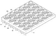
이하, 도 1a 내지 도 11을 참조하여, 본 발명의 제1 실시예에 따른 발광 장치의 제조 방법에 대하여 상세히 설명한다. 도 1a는 본 발명의 제1 실시예에 따른 방법에 의해 제조한 발광 장치를 나타낸 사시도이다. 도 1b는 본 발명의 제1 실시예에 따른 방법에 의해 제조한 발광 장치를 나타낸 저면 사시도이다. 도 2는 도 1a의 A-A'선을 따라 자른 본 발명의 제1 실시예에 따른 방법에 의해 제조한 발광 장치의 단면도이다. 도 3 내지 도 11은 본 발명의 제1 실시예에 따른 발광 장치의 제조 방법을 나타낸 단면도이다. 도 12a 내지 도 12c는 본 발명의 제1 실시예에 따른 발광 장치의 렌즈 지지 패턴과 렌즈를 개략적으로 도시한 도면들이다.Hereinafter, a method of manufacturing the light emitting device according to the first embodiment of the present invention will be described in detail with reference to FIGS. 1A to 11. FIG. 1A is a perspective view illustrating a light emitting device manufactured by a method according to a first embodiment of the present invention. 1B is a bottom perspective view showing a light emitting device manufactured by the method according to the first embodiment of the present invention. FIG. 2 is a cross-sectional view of a light emitting device manufactured by the method according to the first embodiment of the present invention cut along the line A-A 'in FIG. 1A. 3 to 11 are cross-sectional views illustrating a method of manufacturing the light emitting device according to the first embodiment of the present invention. 12A to 12C are views schematically showing a lens support pattern and a lens of a light emitting device according to the first embodiment of the present invention.
먼저, 도 1a, 도 1b, 도 2 및 도 3을 참조하면, 기판(10) 내에 제너 다이오드(zener diode)(20)를 내장(embed)할 수 있다.First, referring to FIGS. 1A, 1B, 2, and 3, a
기판(10)은 예를 들어 사파이어(sapphire) 기판, 실리콘(Si) 기판, 실리콘 카바이드(SiC) 기판, 상부에 질화갈륨이 형성되어 있는 사파이어 기판, 상부에 질화갈륨이 형성되어 있는 실리콘 기판, 상부에 질화갈륨이 형성되어 있는 실리콘 카바이드 기판일 수 있다.The
기판(10)은 불순물이 도핑(doping)되지 않은 미도핑(undoped) 기판일 수 있다.The
이러한 기판(10) 내에 제1 형 불순물을 예를 들어 이온 주입(implant), 열확산(thermal diffusion), 또는 플라즈마 도핑하여 제1 형 반도체 영역(21)을 형성한다. 제1 형 불순물은 예를 들어 P 형 불순물일 수 있다. 제1 형 반도체 영역(21)은 도 1b에 도시한 바와 같이 제1 후면 전극(55a)과 제2 후면 전극(55b) 모두와 오버랩되도록 형성할 수 있다.The first
제1 형 반도체 영역(21) 상에는 제1 형 반도체 영역(21)과 접촉하도록 제1 형 분순물과 반대 도전형을 가지는 제2 형 불순물을 이온 주입, 열확산, 또는 플라즈마 도핑하여 제2 형 반도체 영역(22)을 형성한다. 제2 형 불순물은 예를 들어 N 형 불순물일 수 있으며, 제2 형 반도체 영역(22)은 제1 후면 전극(55a)과 제2 후면 전극(55b)과 각각 오버랩되도록 2 이상 형성할 수 있다.
제1 형 반도체 영역(21)과 제2 형 반도체 영역(22)은 PN 접합을 형성하며 제너 다이오드(20)를 구성한다.The first-
본 실시예와 같이 도핑되지 않은 기판(10)에 제1 형 불순물 및 제2 형 불순물을 각각 이온 주입하여 제너 다이오드(20)를 형성함으로써 각 불순물의 농도를 용이하게 조절할 수 있다. 이 경우 제1 형 불순물은 상대적으로 낮은 농도로 형성 하고, 제2 형 불순물은 상대적으로 높은 농도로 형성할 수 있다. 예를 들어 제1 형 불순물의 농도는 5 × 10¹⁶/ ㎤ 이상 1 × 10¹⁸㎤ 이하일 수 있고, 제2 형 불순물의 농도는 이보다 높아야 한다.The concentration of each impurity can be easily controlled by ion-implanting the first-type impurity and the second-type impurity into the
제너 다이오드(20)는 후술하는 정전기 등에 의해 발광 소자(100)에 과전압이 인가되는 경우 바이패스(by-pass) 전류를 형성하여 발광 소자(100)의 손상을 방지하는 역할을 한다.The Zener
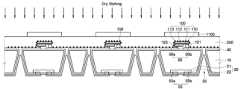
이어서, 도 1a, 도 2 및 도 4를 참조하면, 기판(10)의 일면에 보호 패턴(900)을, 기판(10)의 타면, 즉 상면에 보호막(910)을 각각 형성한다. 이를 위해 기판(10)의 양면에 보호막(910)을 형성한다. 한편, 기판(10)의 일면, 즉 하면의 보호막(미도시) 상에 제1 포토레지스트 패턴(1000)을 형성하고 제1 포토레지스트 패턴(1000)을 식각 마스크로 이용하여 보호막을 식각함으로써 보호 패턴(900)을 형성한다. 여기서, 제1 포토레지스트 패턴(1000) 및 보호 패턴(900)은 발광 소자 실장 영역(I) 및 분리 영역(II)이 형성될 영역에 형성하고, 그루브(groove)(35) 및 관통홀(30)이 형성될 영역을 노출시킨다.Next, referring to FIGS. 1A, 2 and 4, a
기판(10)의 타면, 즉 상면에 보호막(910)이 형성된 이유는 그루브(35) 식각 공정에서 KOH 용액에 기판 상면이 손상을 받지 않도록 하기 위함이고, 제1 포토레지스트 패턴(1000)과 기판(10)의 일면 사이에 보호 패턴(900)이 형성되는 이유는 제1 포토레지스트 패턴(1000)과 동일한 패턴을 형성하여 그루브(35) 식각 공정 시 KOH 용액에 포토레지스트가 용해되면, 보호 패턴(900)을 이용하여 식각 공정을 진 행하기 위함이다. 이러한 보호 패턴(900) 및 보호막(900)은 예를 들어 질화 규소 또는 산화 규소로 이루어질 수 있다.The reason why the
이어서, 도 1a, 도 1b, 도 2, 도 4 및 도 5를 참조하면, 보호 패턴(900)을 식각 마스크로 이용하여 기판(10)의 일면을 식각하여 복수의 발광 소자 실장 영역(I), 분리 영역(II), 및 복수의 발광 소자 실장 영역(I) 사이의 적어도 하나의 그루브(35) 및 관통홀(30)을 형성한다.Next, referring to FIGS. 1A, 1B, 2, 4 and 5, one surface of the
기판(10)의 식각은 예를 들어 습식 식각법을 이용하여 수행할 수 있다. 습식 식각은 예를 들어 KOH 용액과 같은 이방성 습식 식각액을 이용하여 수행할 수 있다. 이에 따라 도 1b에 도시한 바와 같이 습식 식각액에 노출된 기판(10)에는 기판(10)의 일면측에서 타면측으로 갈수록 그루브(35)의 단면 형상이 점점 작아지는 피라미드 형상의 그루브(35)가 형성된다. 도 5에 도시한 바와 같이 그루브(35)의 단면 형상은 "역 V"자일 수 있다. 그루브(35)는 서로 인접한 복수의 발광 소자 실장 영역(I) 사이에 적어도 하나 형성될 수 있다. 본 실시예에서는 서로 인접한 복수의 발광 소자 실장 영역(I) 사이에 2개의 그루브(35)가 형성되어 있는 경우를 예로 들어 설명하였으나, 본 발명은 이에 한정되는 것은 아니다.Etching of the
습식 식각액에 대한 기판(10)의 노출 시간을 조절하면 그루브(35)의 말단에 관통홀(30)이 형성될 수 있다. 또한, 상술한 바와 같이 기판(10)의 타면에 보호막(910)이 형성되어 있기 때문에 습식 식각액에 의해 그루브(35)가 형성되다가 기판(10) 타면의 보호막(910)에 의해 식각이 정지될 수도 있다.By adjusting the exposure time of the
이러한 그루브(35) 및 관통홀(30) 형성 이후, 잔류하는 보호 패턴(910) 및 보호막(900)은 예를 들어 BOE(Buffered Oxide Echant), HF에 의해 제거될 수 있다.이어서, 도 6을 참조하면, 예를 들어 열산화(thermal oxidation)법을 이용하여 노출된 기판(10) 표면에 산화막으로 이루어진 보호막(40)을 형성한다.After the formation of the
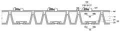
이어서, 도 7을 참조하면, 기판(10)의 일면측에 후면 전극(55)을 형성하고, 기판(10)의 타면측에 전면 전극(50)을 형성한다. 전면 전극(50)과 후면 전극(55)의 형성 순서는 뒤바뀔 수 있다.7, a
전면 전극(50)을 형성하기 위해, 예를 들어 스퍼터링(sputtering)법 또는 전기 도금(electroplating)법을 이용하여 기판(10)의 타면측에 도전성 물질층을 형성한다. 도전성 물질층으로서 도전성이 우수하고 보호막(40)과 접착성이 있는 물질, 예를 들어 Ti, Pt, Au, Cr, Ni, Cu, Ag로 이루어진 단일막 또는 다중막이 이용될 수 있다.A conductive material layer is formed on the other surface side of the
도전성 물질을 패터닝하여 제1 전면 전극(50a)과 제2 전면 전극(50b)를 형성할 수 있다. 이 경우 제1 전면 전극(50a)과 제2 전면 전극(50b)은 서로 이격되도록 패터닝한다.The first
후면 전극(55)은 전면 전극(50)과 동일한 물질 및 공정을 이용하여 형성할 수 있다. 후면 전극(55)은 제1 후면 전극(55a)과 제2 후면 전극(55b)으로 이루어질 수 있다. 기판(10)의 일면측에 형성된 후면 전극(55)은 관통홀(30)을 통해서 전면 전극(50)과 서로 접촉할 수 있다. 구체적으로 제1 후면 전극(55a)은 제1 전면 전극(50a)과 직접 접촉하고, 제2 후면 전극(55b)은 제2 전면 전극(50b)과 직접 접촉할 수 있다.The
도 8을 참조하면, 발광 소자(100)를 형성하고, 전면 전극(50) 상에 발광 소자(100)를 실장한다.Referring to FIG. 8, the
발광 소자(100)는 발광 소자 지지 기판(110) 상에 순차적으로 적층된 제1 도전형의 제1 도전 패턴(111), 발광 패턴(112), 제2 도전형의 제2 도전 패턴(113)을 포함한다.The
각 층에 대해서 구체적으로 설명하면, 제1 도전 패턴(111)은 제1 도전형(예를 들어, n형)이고, 제2 도전 패턴(113)은 제2 도전형(예를 들어, p형)일 수 있으나, 설계 방식에 따라서 제1 도전 패턴(111)이 제2 도전형(p형)이고, 제2 도전 패턴(113)이 제1 도전형(n형)일 수 있다.Specifically, the first
발광 패턴(112)은 제1 도전 패턴(111)의 캐리어(예를 들어, 전자)와 제2 도전 패턴(113)의 캐리어(예를 들어, 홀)가 결합하면서 광을 발생하는 영역이다.The
발광 패턴(112)은 도면으로 정확하게 도시하지는 않았으나, 우물층과 장벽층으로 이루어질 수 있는데, 우물층은 장벽층보다 밴드갭이 작기 때문에, 우물층에 캐리어(전자, 홀)가 모여 결합하게 된다. 이러한 발광 패턴(112)은 우물층의 개수에 따라 단일 양자 우물(Single Quantum Well; SQW) 구조, 다중 양자 우물(Multiple Quantum Well; MQW) 구조로 구분할 수 있다. 단일 양자 우물 구조는 하나의 우물층을 포함하고, 다중 양자 우물 구조는 다층의 우물층을 포함한다. 발광 특성을 조절하기 위해서, 우물층, 장벽층 중 적어도 어느 한 곳에, B, P, Si, Mg, Zn, Se, Al 중 적어도 하나를 도핑할 수 있다.The
도시 하지는 않았으나, 제1 도전 패턴(111) 상에는 제1 전극(미도시)이 형성 될 수 있다. 제1 전극은 투명 또는 불투명 금속으로 이루어질 수 있다. 제1 전극은 인듐 틴 옥사이드(ITO), 구리(Cu), 니켈(Ni), 크롬(Cr), 금(Au), 티타늄(Ti), 백금(Pt), 알루미늄(Al), 바나듐(V), 텅스텐(W), 몰리브덴(Mo), 은(Ag) 중 적어도 하나를 포함할 수 있다.Although not shown, a first electrode (not shown) may be formed on the first
제2 도전 패턴(113) 상에는 제2 전극(미도시)이 형성될 수 있다. 제2 전극은 반사율이 높은 물질, 예를 들어, 은(Ag), 알루미늄(Al) 중 적어도 하나로 이루어질 수 있다.A second electrode (not shown) may be formed on the second
이와 같이 형성된 발광 소자(100)는 예를 들어 플립칩(flip chip) 방식으로 기판(10) 상의 전면 전극(50)에 실장될 수 있다. 발광 소자(100)는 솔더(121, 123)를 이용하여 기판(10)에 실장될 수 있다. 솔더(121, 123)로는 예를 들어 AgSn, PbSn, 또는 AuSn을 이용할 수 있다. 제1 도전 패턴(111)에 연결된 제1 솔더(121)는 제2 전면 전극(50b)에 연결되고, 제2 도전 패턴(113)에 연결된 제2 솔더(123)는 제1 전면 전극(50a)에 연결될 수 있다. 그러나, 각 발광 소자(100)별로 제1 도전 패턴(111)과 제2 도전 패턴(113)이 각각 다른 전면 전극(50)에 연결될 수도 있다. 이와 같이 형성된 발광 소자(100)는 청색광을 발생시키는 청색 발광 소자일 수 있다.The
이어서, 도 1a 및 도 9를 참조하면, 기판(10) 상에 발광 소자(100) 및 전면 전극(50)을 덮는 절연막(200)을 형성한다.Next, referring to FIGS. 1A and 9, an insulating
절연막(200)은 예를 들어 스핀 코팅(spin coating)법, 드롭(drop)법, 스프레이 코팅(spray coating)법을 이용하여 형성할 수 있다. 절연막(200)은 예를 들어 실리콘 수지로 이루어질 수 있으며 발광 소자(100)를 보호하는 역할을 한다. 절연 막(200)은 이후에 설명하는 렌즈 지지 패턴(300)이 형성된 영역과 렌즈 지지 패턴(300)이 형성되지 않은 영역이 단차를 가지도록 100 내지 300㎛의 두께로 형성한다. 본 실시예의 절연막(200)은 단일막으로 형성할 수 있다.The insulating
한편, 절연막(200)에는 형광체(150)가 포함되어 있을 수 있다. 형광체(150)는 절연막(200)을 이루는 실리콘 수지 등에 혼합되어 스핀 코팅법, 드롭법, 스프레이 코팅법에 의해 기판(10) 상에 도포된다.On the other hand, the insulating
본 실시예에서는 형광체(150)가 침전될 때까지 기다렸다가, 실리콘 수지를 경화(curing)시켜 절연막(200)을 형성한다. 이에 따라, 형광체(150)는 침전되어 발광 소자(100)의 상면과 측면 및 기판(10)의 상면을 덮도록 배치되므로 발광 소자(100)에서 출사된 광은 형광체(150)를 거쳐 대기로 방출된다.In this embodiment, the
여기서, 형광체(150)는 청색광의 일부를 파장 변환하여 적색광을 발생시키는 적색 형광체, 청색광의 일부를 파장 변환하여 황색광을 발생시키는 황색 형광체 또는 청색광의 일부를 파장 변환하여 녹색광을 발생시키는 녹색 형광체를 포함할 수 있다.Here, the
형광체(150)는 예를 들어, Eu, Ce 등의 란타노이드계 원소에 의해 주로 활력을 받는 질화물계/산질화물계 형광체, Eu 등의 란타노이드계, Mn 등의 천이 금속계의 원소에 의해 주로 활력을 받는 알칼리토류 할로겐 애퍼타이트 형광체, 알칼리토류 금속 붕산 할로겐 형광체, 알칼리토류 금속 알루민산염 형광체, 알칼리토류 규산염, 알칼리토류 유화물, 알칼리토류 티오갈레이트, 알칼리토류 질화 규소, 게르만산염, 또는 Ce 등의 란타노이드계 원소에 의해 주로 활력을 받는 희토류 알루민 산염, 희토류 규산염 또는 Eu 등의 란타노이드계 원소에 의해 주로 활력을 받는 유기 및 유기 착체 등에서 선택되는 적어도 어느 하나 이상일 수 있다. 구체적인 예로서 아래와 같은 형광체를 사용할 수가 있지만 이에 한정되지 않는다.The
Eu, Ce 등의 란타노이드계 원소에 의해 주로 활력을 받는 질화물계 형광체는 M2Si5N8:Eu(M는 Sr, Ca, Ba, Mg, Zn에서 선택되는 적어도 하나) 등이 있다. 또, M2Si5N8:Eu 외, MSi7N10:Eu, M1.8Si5O0.2N8:Eu, M0.9Si7O0.1N10:Eu(M는 Sr, Ca, Ba, Mg, Zn에서 선택되는 적어도 하나) 등도 있다.The nitride-based fluorescent material mainly activated by lanthanoid elements such as Eu and Ce is M2 Si5 N8 : Eu (M is at least one selected from Sr, Ca, Ba, Mg and Zn). Further, M2Si5 N8: Eu etal, MSi 7 N 10: Eu, M 1 .8 Si 5 O 0 .2 N 8: Eu, M 0 .9 Si 7 O 0 .1 N 10: Eu (M is Sr , At least one selected from Ca, Ba, Mg, and Zn).
Eu, Ce 등의 란타노이드계 원소에 의해 주로 활력을 받는 산질화물계 형광체는 MSi2O2N2:Eu(M는 Sr, Ca, Ba, Mg, Zn에서 선택되는 적어도 하나) 등이 있다.Examples of oxynitride-based fluorescent materials that are mainly energized by lanthanoid elements such as Eu and Ce include MSi2 O2 N2 : Eu (M is at least one selected from Sr, Ca, Ba, Mg, and Zn).
Eu 등의 란타노이드계, Mn 등의 천이 금속계의 원소에 의해 주로 활력을 받는 알칼리토류 할로겐 애퍼타이트 형광체에는 M5(PO4)3 X:R(M는 Sr, Ca, Ba, Mg, Zn에서 선택되는 적어도 하나, X는 F, Cl, Br, I에서 선택되는 적어도 하나, R는 Eu, Mn, Eu에서 선택된 적어도 하나) 등이 있다.Lanthanide, an alkali earth halogen apatite phosphor subjected to mainly energized by the elements of the transition metal-based, such as Mn, such as Eu isM 5 (PO 4) 3 X : R (M is at the Sr, Ca, Ba, Mg, Zn X is at least one selected from F, Cl, Br and I, and R is at least one selected from Eu, Mn and Eu).
알칼리토류 금속 붕산 할로겐 형광체에는 M2B5O9X:R(M는 Sr, Ca, Ba, Mg, Zn에서 선택되는 적어도 하나, X는 F, Cl, Br, I에서 선택되는 적어도 하나, R는 Eu, Mn, Eu에서 선택된 적어도 하나) 등이 있다.Alkaline earth metal boric acid halogen phosphor,M 2 B 5 O 9 X: R (M is Sr, Ca, Ba, Mg, at least one element selected from Zn, X is F, Cl, Br, at least one, R is selected from I Is at least one selected from Eu, Mn and Eu).
알칼리토류 금속 알루민산염 형광체에는 SrAl2O4:R, Sr4Al14O25:R, CaAl2O4:R, BaMg2Al16O27:R, BaMg2Al16O12:R, BaMgAl10O17:R(R는 Eu, Mn, Eu에서 선택된 어느 하나) 등이 있다.The alkaline earth metal aluminate phosphors include SrAl2 O4 : R, Sr4 Al14 O25 : R, CaAl2 O4 : R, BaMg2 Al16 O27 : R, BaMg2 Al16 O12 :10 O17 : R (R is any one selected from Eu, Mn and Eu).
알칼리토류 유화물 형광체에는 La2O2S:Eu, Y2O2S:Eu, Gd2O2S:Eu 등이 있다.The alkaline earth emulsion phosphors include La2 O2 S: Eu, Y2 O2 S: Eu, and Gd2 O2 S: Eu.
Ce 등의 란타노이드계 원소에 의해 주로 활력을 받는 희토류 알루민산염 형광체에는 Y3Al5O12:Ce, (Y0.8Gd0.2)3Al5O12:Ce, Y3(Al0.8Ga0.2)5 O12:Ce, (Y, Gd)3 (Al, Ga)5 O12의 조성식에서 나타내어지는 YAG계 형광체 등이 있다. 또한, Y의 일부 혹은 전부를 Tb, Lu 등으로 치환한 Tb3Al5O12:Ce, Lu3Al5O12:Ce 등도 있다.By a lanthanoid element such as Ce rare-earth aluminate phosphor mainly receives energy, theY 3 Al 5 O 12: Ce , (Y 0 .8 Gd 0 .2) 3 Al 5 O 12: Ce, Y 3 (Al0 .8 Ga 0 .2) 5 O 12: there isCe, (Y, Gd) 3 (Al, Ga) YAG -base phosphor represented by a composition formula of in5 O12 and the like. Further, Tb3 Al5 O12 : Ce and Lu3 Al5 O12 : Ce in which a part or all of Y is substituted with Tb, Lu, and the like are also available.
알칼리토류 규산염 형광체에는 실리케이트(silicate)로 구성될 수있으며, 대표적인 형광체로 (SrBa)2SiO4:Eu 등이 있다.The alkaline earth silicate phosphor may be composed of silicate, and (SrBa)2 SiO4 : Eu is a typical phosphor.
그 외의 형광체에는 ZnS:Eu, Zn2GeO4:Mn, MGa2S4:Eu(M는 Sr, Ca, Ba, Mg, Zn에서 선택되는 적어도 하나, X는 F, Cl, Br, I에서 선택되는 적어도 하나) 등이 있다.Other phosphors include ZnS: Eu, Zn2 GeO4 : Mn, MGa2 S4 : Eu where M is at least one selected from Sr, Ca, Ba, Mg and Zn and X is selected from F, Cl, Br and I At least one of them).
전술한 형광체는 희망하는 바에 따라 Eu에 대신하거나 또는 Eu에 더하여 Tb, Cu, Ag, Au, Cr, Nd, Dy, Co, Ni, Ti에서 선택되는 1종 이상을 함유시킬 수도 있다.The above-mentioned phosphors may contain at least one selected from Tb, Cu, Ag, Au, Cr, Nd, Dy, Co, Ni and Ti in place of or in addition to Eu as desired.
또한, 전술한 형광체 이외의 형광체로서, 동일한 성능, 효과를 갖는 형광체도 사용할 수 있다.Further, as a phosphor other than the above-mentioned phosphor, a phosphor having the same performance and effect can also be used.
도 1a, 도 9 및 도 10을 참조하면, 렌즈 지지 패턴(300)이 형성될 영역에 제2 포토레지스트 패턴(1100)을 형성한다.Referring to FIGS. 1A, 9 and 10, a
본 실시예의 제2 포토레지스트 패턴(1100)은 수평 단면이 원형이 되도록 형성할 수 있다.The
이어서, 제2 포토레지스트 패턴(1100)을 식각 마스크로 이용하여 렌즈 지지 패턴(300)이 형성될 영역을 제외한 영역의 절연막(200)을 적어도 일부 식각한다. 이 경우 렌즈 지지 패턴(300)이 형성될 영역을 제외한 절연막(200)을 전부 식각하여 제거할 수 있다. 절연막(200)의 식각은 건식 식각(dry etching)법을 이용할 수 있다. 이에 따라 절연막(200)이 기판(10)의 표면에 수직인 방향으로 식각된다.Next, the insulating
이와 같이 하면 도 11에 도시한 바와 같이, 발광 소자(100) 상부에 렌즈 지지 패턴(300)이 형성되고, 렌즈 지지 패턴(300)이 형성된 영역 이외의 영역, 예를 들어 분리 영역(II) 상의 절연막(200)은 전부 제거된다. 이 경우 도 1a에 도시한 바와 같이, 제2 포토레지스트 패턴(1100)의 형상에 따라 렌즈 지지 패턴(300)은 원기둥 형상으로 형성될 수 있다.11, a
이 경우 렌즈 지지 패턴(300)은 분리 영역(II)의 표면과 단차(s)를 가진다. 렌즈 지지 패턴(300)과 분리 영역(II)이 이루는 단차(s)는 100 내지 300㎛일 수 있다. 렌즈 지지 패턴(300)의 폭은 후술하는 렌즈(400)의 표면 장력을 증가시키는 역할을 한다. 또한, 분리 영역(II)에 절연막(200)이 잔류하지 않으므로 발광 장치를 단위 발광 소자(100)별로 절단(scribe)하거나, 발광 소자(100) 어레이별로 절단하는 경우 절단면에 절연막(200)이 형성되지 않아 후술하는 렌즈(400)가 파손될 위험을 감소시킬 수 있다. 이와 같이 렌즈(400)와 절연막(200)을 별도로 형성하면, 렌즈(400)와 절연막(200)을 하나의 시트로 형성하여 기판(10)에 부착하는 경우에 비 해 발광 소자(100) 절단 공정을 용이하게 하고, 렌즈(400) 파손 위험을 현저히 감소시킬 수 있다.In this case, the
이어서, 도 1a, 도 2, 및 도 12a 내지 도 12c를 참조하면, 렌즈 지지 패턴(300) 상에 렌즈(400)를 형성한다. 렌즈(400)는 발광 소자(100)로부터 출사된 광을 집광하는 역할을 한다.Next, referring to FIGS. 1A, 2, and 12A to 12C, a
도 1a 및 도 2를 참조하면, 렌즈(400) 형성 공정은 예를 들어 잉크젯(inkjet)법을 이용할 수 있다. 구체적으로 렌즈(400) 형성 공정은 마이크로 잉크젯법을 이용하여 렌즈(400)를 전부 덮고, 렌즈 지지 패턴(300)의 상면의 적어도 일부를 덮도록 형성할 수 있다. 또한, 렌즈 지지 패턴(300)과 분리 영역(II)이 단차에 따라 렌즈 지지 패턴(300)의 측면의 일부를 덮도록 렌즈(400)를 형성할 수도 있다.Referring to FIGS. 1A and 2, the
본 실시예의 렌즈(400)는 렌즈 지지 패턴(300)의 상면 가장 자리에 형성되는 표면 장력으로 인해 반구형으로 형성될 수 있다. 즉, 원형 단면을 가지는 렌즈 지지 패턴(300)의 상면 형상을 따라 렌즈(400)의 저면은 원형 단면을 가지고 렌즈(400)의 입체 형상은 반구형으로 형성될 수 있다.The
도 12a 내지 도 12c를 참조하면, 렌즈 지지 패턴(300)의 폭(w1, w2, w3)이 증가할수록 동일한 부피의 실리콘 수지로 이루어진 렌즈(400)의 곡률 반경이 커짐을 확인할 수 있다.12A to 12C, it can be seen that as the widths w1, w2 and w3 of the
구체적으로 설명하면, 도 12a에 도시한 바와 같이, 렌즈 지지 패턴(300)의 폭(w1)이 좁은 경우 렌즈(400)의 높이(H1)는 높다. 이 경우 렌즈(400)는 광의 직진 성을 향상시킬 수 있다. 도 12b 및 도 12c에 도시한 바와 같이 렌즈 지지 패턴(300)의 폭(w2, w3)이 증가하면, 도 12a와 동일 부피의 실리콘 수지로 이루어진 도 12b 및 도 12c의 렌지 지지 패턴(300)의 표면 장력은 점점 커지며, 렌즈(400)의 높이(H2, H3)는 점점 낮아진다. 도 12c와 같이 곡률 반경이 큰 렌즈(400)는 광의 퍼짐성이 향상된다.More specifically, as shown in FIG. 12A, when the width w1 of the
즉, 렌즈 지지 패턴(300)의 상면 가장 자리에 인가되는 표면 장력에 의해 렌즈(400)의 형상이 유지되므로, 렌즈 지지 패턴(300) 및 이에 따른 렌즈(400)의 곡률 반경을 조절하여 용도에 맞는 렌즈(400)를 형성할 수 있다.That is, since the shape of the
다시, 도 1a 및 도 2를 참조하면, 렌즈(400)는 렌즈 지지 패턴(300)보다 굴절률이 작거나 같은 물질로 이루어질 수 있다. 다시 말해 렌즈 지지 패턴(300)의 굴절률이 렌즈(400)보다 크거나 같을 수 있다. 이에 따라 발광 소자(100)로부터 출사한 광이 렌즈 지지 패턴(300), 렌즈(400), 및 공기층을 순차적으로 통과하게 된다. 이 경우 렌즈 지지 패턴(300), 렌즈(400), 및 공기층의 굴절률은 순차적으로 감소하므로 굴절률의 급격한 감소로 인한 전반사 현상을 감소시킬 수 있어 광 출사 효율을 향상시킬 수 있다.Referring again to FIGS. 1A and 2, the
이어서, 렌즈(400)를 큐어링시켜 렌즈(400)를 견고하게 할 수 있다.Then, the
이어서, 각 발광 소자(100)별 또는 발광 소자(100) 어레이별로 기판(10)을 절단할 수 있다. 발광 소자(100) 어레이별로 절단되어 형성된 발광 장치의 각 발광 소자(100)는 레드(red), 그린(green), 블루(blue) 계열의 색상을 발광할 수 있으며, 이들이 주기적으로 배열되어 형성될 수 있다.Subsequently, the
이하, 도 2 내지 도 11 및 도 13을 참조하여, 본 발명의 제1 실시예의 일 변형례에 따른 발광 장치의 제조 방법에 대하여 상세히 설명한다. 도 13은 본 발명의 제1 실시예의 다른 변형례에 따른 방법에 의해 제조한 발광 장치를 나타낸 사시도이다. 이하의 실시예 및 변형례들에서는 이전의 실시예와 동일한 구성 요소에 대해서는 동일한 참조 번호를 부여하고, 설명을 생략하거나 간략화한다.Hereinafter, a method of manufacturing a light emitting device according to a first modification of the first embodiment of the present invention will be described in detail with reference to FIGS. 2 to 11 and FIG. 13 is a perspective view showing a light emitting device manufactured by a method according to another modification of the first embodiment of the present invention. In the following embodiments and modifications, the same reference numerals are given to the same constituent elements as those of the previous embodiment, and the description thereof is omitted or simplified.
도 3 내지 도 11에서 설명한 공정을 이용하여, 발광 장치를 형성한다.The light emitting device is formed by using the processes described in Figs. 3 to 11.
이 경우, 도 10의 포토레지스트 패턴(1100)의 수평 단면 형상은 사각형 형상일 수 있다. 이에 따라, 도 13에 도시한 바와 같이 렌즈 지지 패턴(300')은 사각 기둥 형상을 가지도록 형성되며, 렌즈(400')는 모서리가 곡선으로 형성된 사각뿔 형상을 가지도록 형성된다.In this case, the horizontal cross-sectional shape of the
이하, 도 2 내지 도 11 및 도 14를 참조하여, 본 발명의 제1 실시예의 다른 변형례에 따른 발광 장치의 제조 방법에 대하여 상세히 설명한다. 도 14는 본 발명의 제1 실시예의 다른 변형례에 따른 방법에 의해 제조한 발광 장치를 나타낸 사시도이다.Hereinafter, a manufacturing method of a light emitting device according to another modification of the first embodiment of the present invention will be described in detail with reference to FIGS. 2 to 11 and FIG. 14 is a perspective view showing a light emitting device manufactured by a method according to another modification of the first embodiment of the present invention.
도 3 내지 도 11에서 설명한 공정을 이용하여, 발광 장치를 형성한다.The light emitting device is formed by using the processes described in Figs. 3 to 11.
이 경우, 도 10의 포토레지스트 패턴(1100)의 수평 단면 형상은 삼각형 형상일 수 있다. 이에 따라, 도 14에 도시한 바와 같이 렌즈 지지 패턴(300'')은 삼각 기둥 형상을 가지도록 형성되며, 렌즈(400'')는 모서리가 곡선으로 형성된 삼각뿔 형상을 가지도록 형성된다.In this case, the horizontal cross-sectional shape of the
본 발명의 렌즈 및 렌즈 지지 패턴의 형상은 이상의 실시예 및 변형례에서 설명한 형상에 한정되지 않으며 다양한 변형이 가능하다.The shape of the lens and the lens support pattern of the present invention is not limited to the shape described in the above embodiments and modifications, and various modifications are possible.
이어서, 도 3 내지 도 7, 도 9 내지 도 11, 도 15, 및 도 16을 참조하여, 본 발명의 제2 실시예에 따른 발광 장치의 제조 방법에 대하여 상세히 설명한다. 도 15 및 도 16은 본 발명의 제2 실시예에 따른 발광 장치의 제조 방법을 나타낸 단면도이다.Next, a method of manufacturing the light emitting device according to the second embodiment of the present invention will be described in detail with reference to FIGS. 3 to 7, 9 to 11, 15, and 16. 15 and 16 are cross-sectional views illustrating a method of manufacturing a light emitting device according to a second embodiment of the present invention.
먼저, 도 3 내지 도 7에서 설명한 공정을 이용하여, 발광 소자 실장 영역(I), 분리 영역(II)을 형성하고, 전면 전극(50) 및 후면 전극(55)을 형성한다.First, the light emitting element mounting region I and the isolation region II are formed by using the processes described in FIGS. 3 to 7, and the
이어서, 도 15를 참조하면, 발광 소자(101)를 전면 전극(50)에 전기적으로 접속시킨다. 본 실시예의 발광 소자(101)는 순차적으로 적층된 제1 도전형의 제1 도전 패턴(114), 발광 패턴(115), 제2 도전형의 제2 도전 패턴(116)을 포함한다. 본 실시예의 발광 소자(101)는 제1 도전 패턴(114)은 제1 전면 전극(50a)에 직접 연결되고 제2 도전 패턴(116)은 와이어(wire)(126)에 의해 제2 전면 전극(50b)에 연결될 수 있다. 제1 도전 패턴(114)과 제2 도전 패턴(116)은 각 발광 소자(100)별로 서로 다른 전면 전극(50)에 연결될 수도 있다.Next, referring to FIG. 15, the
이어서, 도 8 내지 도 11에서 설명한 공정을 따라 도 16에 도시한 바와 같은 발광 장치를 완성한다.Then, a light emitting device as shown in Fig. 16 is completed according to the steps described in Figs. 8 to 11.
본 실시예의 발광 장치는 본 발명의 제1 실시예의 일 변형례 및 본 발명의 제1 실시예의 타 변형례와 조합될 수 있으며, 본 발명의 다른 실시예 및 변형례들도 서로 조합될 수 있음은 물론이다.The light emitting device of this embodiment can be combined with one modification of the first embodiment of the present invention and the other modification of the first embodiment of the present invention, and other embodiments and modifications of the present invention can be combined with each other Of course.
이어서, 도 3 내지 도 7, 도 9 내지 도 11, 도 17 및 도 18을 참조하여, 본 발명의 제3 실시예에 따른 발광 장치의 제조 방법에 대하여 상세히 설명한다. 도 17 및 도 18은 본 발명의 제3 실시예에 따른 발광 장치의 제조 방법을 나타낸 단면도이다.Next, a method of manufacturing the light emitting device according to the third embodiment of the present invention will be described in detail with reference to FIGS. 3 to 7, 9 to 11, 17, and 18. 17 and 18 are cross-sectional views illustrating a method of manufacturing a light emitting device according to a third embodiment of the present invention.
먼저, 도 3 내지 도 7에서 설명한 공정을 이용하여, 발광 소자 실장 영역(I), 분리 영역(II)을 형성하고, 전면 전극(50) 및 후면 전극(55)을 형성한다.First, the light emitting element mounting region I and the isolation region II are formed by using the processes described in FIGS. 3 to 7, and the
이어서, 도 17을 참조하면, 발광 소자(102)를 전면 전극(50)에 전기적으로 접속시킨다. 본 실시예의 발광 소자(102)는 순차적으로 적층된 제1 도전형의 제1 도전 패턴(117), 발광 패턴(118), 제2 도전형의 제2 도전 패턴(119)을 포함한다. 본 실시예의 발광 소자(102)는 제1 도전 패턴(117)은 제1 와이어(127)에 의해 제2 전면 전극(50b)에 연결되고, 제2 도전 패턴(119)은 제2 와이어(129)에 의해 제1 전면 전극(50a)에 연결될 수 있다. 제1 도전 패턴(117)과 제2 도전 패턴(119)은 각 발광 소자(100)별로 서로 다른 전면 전극(50)에 연결될 수도 있다.Next, referring to FIG. 17, the
이어서, 도 8 내지 도 11에서 설명한 공정을 따라 도 18에 도시한 발광 장치를 완성한다.Next, the light emitting device shown in Fig. 18 is completed according to the steps described in Figs.
이하, 도 3 내지 도 8, 및 도 19 내지 도 22를 참조하여, 본 발명의 제4 실시예에 따른 발광 장치에 대하여 상세히 설명한다. 도 19 내지 도 22는 본 발명의 제4 실시예에 따른 발광 장치의 제조 방법을 나타낸 단면도이다.Hereinafter, the light emitting device according to the fourth embodiment of the present invention will be described in detail with reference to FIGS. 3 to 8 and 19 to 22. FIG. 19 to 22 are cross-sectional views illustrating a method of manufacturing a light emitting device according to a fourth embodiment of the present invention.
먼저, 도 3 내지 도 8에서 설명한 공정을 이용하여, 발광 소자 실장 영역(I), 분리 영역(II), 전면 전극(50)과 후면 전극(55)을 형성한다. 이어서, 전면 전극(50)에 발광 소자(100)를 실장한다.First, the light emitting element mounting region I, the isolation region II, the
이어서, 도 19를 참조하면, 기판(10) 상에 발광 소자(100) 및 전면 전극(50)을 덮는 절연막(200)을 형성한다. 이 경우 절연막(200)에는 형광체(150)가 분산되어 있다.19, an insulating
본 실시예에서는 형광체(153)가 분산된 실리콘 수지를 기판(10) 상에 도포한 후 본 발명의 제1 실시예와 달리 형광체(153)가 침전될 때까지 기다리지 않고 실리콘 수지를 경화시킨다. 이에 따라 기판(10)의 표면 부위 뿐만 아니라 전체의 두께에 걸쳐 형광체(150)가 분산된 절연막(200)을 형성할 수 있다.In this embodiment, after the silicon resin in which the
이어서, 도 20을 참조하면, 제2 포토레지스트 패턴(1100)을 형성하고 이를 식각 마스크로 이용하여 형광체(153)가 분산된 절연막(200)의 적어도 일부를 건식 식각한다.20, a
이와 같이 하면, 도 21에 도시한 바와 같이 발광 소자(100)를 덮는 렌즈 지지 패턴(300)이 형성되고, 형광체(153)는 렌즈 지지 패턴(300) 내부의 전체 영역에 분산되어 있다.21, the
이어서, 도 22를 참조하면, 렌즈 지지 패턴(300) 상에 렌즈(400)를 형성하여, 발광 장치를 완성한다. 본 실시예의 발광 장치는, 발광 소자(100) 주위에 방사상으로 형광체(153)가 형성되어 있다.22, a
이하, 도 3 내지 도 11, 및 도 23을 참조하여, 본 발명의 제5 실시예에 따른 발광 장치에 대하여 상세히 설명한다. 도 23은 본 발명의 제5 실시예에 따른 발광 장치의 제조 방법을 나타낸 단면도이다.Hereinafter, a light emitting device according to a fifth embodiment of the present invention will be described in detail with reference to FIGS. 3 to 11 and FIG. 23 is a cross-sectional view illustrating a method of manufacturing a light emitting device according to a fifth embodiment of the present invention.
먼저, 도 3 내지 도 8에서 설명한 공정을 이용하여, 발광 소자 실장 영 역(I), 분리 영역(II), 전면 전극(50)과 후면 전극(55)을 형성한다. 이어서, 전면 전극(50)에 발광 소자(100)를 실장한다.이어서, 도 23을 참조하면, 형광체(150)를 기판(10) 상에 도포한다. 이 경우 형광체(150)는 휘발성 물질, 예를 들어 아세톤(acetone)에 용해시켜 도포할 수 있다. 이후, 아세톤을 가열하여 휘발시켜 제거한다. 이에 따라 형광체(150)는 기판(10) 상면 및 발광 소자(100)의 상면과 측면을 덮도록 배치되어 발광 소자(100)에서 출사된 광이 형광체(150)를 거쳐 대기로 방출된다.First, the light emitting element mounting region I, the isolation region II, the
이어서, 도 9를 참조하면, 형광체(150) 상에 절연막(200)을 도포한다. 즉, 본 실시예의 형광체(150)는 절연막(200)의 하부에 배치된다.Next, referring to FIG. 9, the insulating
이어서, 도 10, 도 11 및 도 2에서 설명한 공정을 이용하여, 본 실시예의 발광 장치를 완성한다.Next, the light emitting device of this embodiment is completed by using the processes described in Figs. 10, 11, and 2. Fig.
이하, 도 3 내지 도 8, 도 10, 도 11, 도 24 및 도 25를 참조하여, 본 발명의 제6 실시예에 따른 발광 장치에 대하여 상세히 설명한다. 도 24 및 도 25는 본 발명의 제6 실시예에 따른 발광 장치의 제조 방법을 나타낸 단면도이다.Hereinafter, the light emitting device according to the sixth embodiment of the present invention will be described in detail with reference to FIGS. 3 to 8, 10, 11, 24, and 25. FIG. 24 and 25 are cross-sectional views illustrating a method for manufacturing a light emitting device according to a sixth embodiment of the present invention.
먼저, 도 3 내지 도 8에서 설명한 공정을 이용하여, 발광 소자 실장 영역(I), 분리 영역(II), 전면 전극(50)과 후면 전극(55)을 형성한다. 이어서, 전면 전극(50)에 발광 소자(100)를 실장한다.First, the light emitting element mounting region I, the isolation region II, the
이어서, 도 24를 참조하면, 기판(10) 상에 발광 소자(100) 및 전면 전극(50)을 덮는 절연막(200)을 형성한다.24, an insulating
이어서, 절연막(200) 상에 형광체(154)를 도포한다. 형광체(154)의 도포는 본 발명의 제5 실시예와 동일한 방식으로 형성할 수 있다.Subsequently, the
이어서, 도 10, 및 도 11에서 설명한 공정을 이용하여 도 25에 도시한 발광 장치를 형성한다. 본 실시예는 형광체(154)가 렌즈(400)와 절연막(200) 사이에 개재된다.Next, the light emitting device shown in Fig. 25 is formed by using the processes described in Figs. 10 and 11. In this embodiment, the
이하, 도 3 내지 도 8 및 도 26 내지 도 31을 참조하여, 본 발명의 제7 실시예에 따른 발광 장치에 대하여 상세히 설명한다. 도 26은 본 발명의 제7 실시예에 따른 방법에 의해 제조한 발광 장치를 나타낸 사시도이다. 도 27은 도 26의 B-B'선을 따라 자른 본 발명의 제7 실시예에 따른 방법에 의해 제조한 발광 장치의 단면도이다. 도 28 내지 도 31은 본 발명의 제4 실시예에 따른 발광 장치의 제조 방법을 나타낸 단면도이다.Hereinafter, the light emitting device according to the seventh embodiment of the present invention will be described in detail with reference to FIGS. 3 to 8 and 26 to 31. FIG. 26 is a perspective view showing a light emitting device manufactured by the method according to the seventh embodiment of the present invention. FIG. 27 is a cross-sectional view of a light emitting device manufactured by the method according to the seventh embodiment of the present invention cut along the line B-B 'in FIG. 26; 28 to 31 are cross-sectional views illustrating a method of manufacturing a light emitting device according to a fourth embodiment of the present invention.
먼저, 도 3 내지 도 8에서 설명한 공정을 이용하여, 발광 소자 실장 영역(I), 분리 영역(II), 전면 전극(50)과 후면 전극(55)을 형성한다. 이어서, 전면 전극(50)에 발광 소자(100)를 실장한다.First, the light emitting element mounting region I, the isolation region II, the
이어서, 도 26 내지 도 28을 참조하면, 기판(10) 상에 발광 소자(100) 및 전면 전극(50)을 덮는 절연막(203)을 형성한다.26 to 28, an insulating
본 실시예의 절연막(203)은 복수층으로 형성할 수 있다. 즉, 기판(10) 상에 제1 절연막(210) 및 제2 절연막(220)을 순차적으로 적층하여 절연막(203)을 형성할 수 있다. 이 경우 제1 절연막(210)은 제2 절연막(220)보다 굴절률이 크거나 같은 물질로 이루어질 수 있다.The insulating
이어서, 도 26 및 도 29를 참조하면, 렌즈 지지 패턴(303)이 형성될 영역에 제2 포토레지스트 패턴(1100)을 형성한다.Next, referring to FIGS. 26 and 29, a
이어서, 본 발명의 제1 실시예에서 설명한 공정으로 제2 포토레지스트 패턴(1200)을 식각 마스크로 사용하여 렌즈 지지 패턴(303)이 형성될 영역을 제외한 영역의 제2 절연막(220)을 전부 식각하여 제거할 수 있다. 이와 같이 하면 렌즈 지지 패턴(303)이 형성될 영역을 제외한 영역의 제2 절연막(220)은 전부 제거되고 그 하부의 제1 절연막(210)이 노출된다.Then, the second insulating
이어서, 도 30을 참조하면, 제3 포토레지스트 패턴(1200)을 형성한다. 제3 포토레지스트 패턴(1200)은 제2 포토레지스트 패턴(1100)과 동일한 위치에 형성하되 제2 포토레지스트 패턴(1100)보다 폭이 넓을 수 있다. 이어서, 제3 포토레지스트 패턴(1200)을 식각 마스크로 사용하여 렌즈 지지 패턴(303)이 형성될 영역을 제외한 영역의 제1 절연막(210)을 적어도 일부 식각한다. 이 경우 제2 절연막(220)은 전부 식각하여 제거할 수 있다. 이에 따라 도 31에 도시한 바와 같이 제1 렌즈 지지 패턴(310)과 제2 렌즈 지지 패턴(320)으로 이루어진 렌즈 지지 패턴(303)이 형성된다. 제1 렌즈 지지 패턴(310)과 제2 렌즈 지지 패턴(320)은 단차를 가지도록 형성된다.Next, referring to FIG. 30, a
이어서, 도 27을 참조하면, 예를 들어 잉크젯법을 이용하여 렌즈 지지 패턴(303) 상에 렌즈(403)를 형성한다.Next, referring to FIG. 27, a
렌즈(400)는 제2 렌즈 지지 패턴(320)의 상면 및 측면을 전부 덮도록 형성될 수 있다. 또한, 렌즈(403)는 제1 렌즈 지지 패턴(310)의 측면의 일부 및 상면을 더 덮을 수도 있다.The
제1 렌즈 지지 패턴(310)과 제2 렌즈 지지 패턴(320)이 단차를 가지도록 형성될 수 있다. 한편, 제2 렌즈 지지 패턴(303)은 렌즈(403)보다 굴절률이 크거나 같은 물질로 이루어질 수 있다. 또한, 제1 렌즈 지지 패턴(310)은 제2 렌즈 지지 패턴(320)보다 굴절률이 크거나 같은 물질로 이루어질 수 있다. 이에 따라 발광 소자(100)로부터 출사한 광이 제1 렌즈 지지 패턴(310), 제2 렌즈 지지 패턴(320), 렌즈(403), 및 공기층을 순차적으로 통과하게 된다. 이 경우 제1 렌즈 지지 패턴(310), 제2 렌즈 지지 패턴(320), 렌즈(403), 및 공기층의 굴절률은 순차적으로 감소하므로 굴절률의 급격한 감소로 인한 전반사 현상을 감소시킬 수 있어 광 출사 효율을 보다 향상시킬 수 있다.The first
이어서, 렌즈(403)를 큐어링시켜 렌즈(403)를 견고하게 할 수 있다.Then, the
이어서, 각 발광 소자(100)별 또는 발광 소자(100) 어레이별로 기판(10)을 절단할 수 있다.Subsequently, the
이상 첨부된 도면을 참조하여 본 발명의 실시예를 설명하였지만, 본 발명이 속하는 기술분야에서 통상의 지식을 가진 자는 본 발명이 그 기술적 사상이나 필수적인 특징을 변경하지 않고서 다른 구체적인 형태로 실시될 수 있다는 것을 이해할 수 있을 것이다. 그러므로 이상에서 기술한 실시예들은 모든 면에서 예시적인 것이며 한정적이 아닌 것으로 이해해야만 한다.While the present invention has been described in connection with what is presently considered to be practical exemplary embodiments, it is to be understood that the invention is not limited to the disclosed embodiments, but, on the contrary, You will understand. It is therefore to be understood that the above-described embodiments are illustrative in all aspects and not restrictive.
도 1a는 본 발명의 제1 실시예에 따른 방법에 의해 제조한 발광 장치를 나타낸 사시도이다.1A is a perspective view illustrating a light emitting device manufactured by a method according to a first embodiment of the present invention.
도 1b는 본 발명의 제1 실시예에 따른 방법에 의해 제조한 발광 장치를 나타낸 저면 사시도이다.1B is a bottom perspective view showing a light emitting device manufactured by the method according to the first embodiment of the present invention.
도 2는 도 1a의 A-A'선을 따라 자른 본 발명의 제1 실시예에 따른 방법에 의해 제조한 발광 장치의 단면도이다.FIG. 2 is a cross-sectional view of a light emitting device manufactured by the method according to the first embodiment of the present invention cut along the line A-A 'in FIG. 1A.
도 3 내지 도 11은 본 발명의 제1 실시예에 따른 발광 장치의 제조 방법을 나타낸 단면도이다.3 to 11 are cross-sectional views illustrating a method of manufacturing the light emitting device according to the first embodiment of the present invention.
도 12a 내지 도 12c는 본 발명의 제1 실시예에 따른 발광 장치의 렌즈 지지 패턴과 렌즈를 개략적으로 도시한 도면들이다.12A to 12C are views schematically showing a lens support pattern and a lens of a light emitting device according to the first embodiment of the present invention.
도 13은 본 발명의 제1 실시예의 일 변형례에 따른 방법에 의해 제조한 발광 장치를 나타낸 사시도이다.13 is a perspective view showing a light emitting device manufactured by a method according to a first modification of the first embodiment of the present invention.
도 14는 본 발명의 제1 실시예의 다른 변형례에 따른 방법에 의해 제조한 발광 장치를 나타낸 사시도이다.14 is a perspective view showing a light emitting device manufactured by a method according to another modification of the first embodiment of the present invention.
도 15 및 도 16은 본 발명의 제2 실시예에 따른 발광 장치의 제조 방법을 나타낸 단면도이다.15 and 16 are cross-sectional views illustrating a method of manufacturing a light emitting device according to a second embodiment of the present invention.
도 17 및 도 18은 본 발명의 제3 실시예에 따른 발광 장치의 제조 방법을 나타낸 단면도이다.17 and 18 are cross-sectional views illustrating a method of manufacturing a light emitting device according to a third embodiment of the present invention.
도 19 내지 도 22는 본 발명의 제4 실시예에 따른 발광 장치의 제조 방법을 나타낸 단면도이다.19 to 22 are cross-sectional views illustrating a method of manufacturing a light emitting device according to a fourth embodiment of the present invention.
도 23은 본 발명의 제5 실시예에 따른 발광 장치의 제조 방법을 나타낸 단면도이다.23 is a cross-sectional view illustrating a method of manufacturing a light emitting device according to a fifth embodiment of the present invention.
도 24 및 도 25는 본 발명의 제6 실시예에 따른 발광 장치의 제조 방법을 나타낸 단면도이다.24 and 25 are cross-sectional views illustrating a method for manufacturing a light emitting device according to a sixth embodiment of the present invention.
도 26은 본 발명의 제4 실시예에 따른 방법에 의해 제조한 발광 장치를 나타낸 사시도이다.26 is a perspective view showing a light emitting device manufactured by the method according to the fourth embodiment of the present invention.
도 27은 도 26의 B-B'선을 따라 자른 본 발명의 제4 실시예에 따른 방법에 의해 제조한 발광 장치의 단면도이다.27 is a cross-sectional view of the light emitting device manufactured by the method according to the fourth embodiment of the present invention cut along the line B-B 'in FIG.
도 28 내지 도 31은 본 발명의 제4 실시예에 따른 발광 장치의 제조 방법을 나타낸 단면도이다.28 to 31 are cross-sectional views illustrating a method of manufacturing a light emitting device according to a fourth embodiment of the present invention.
(도면의 주요부분에 대한 부호의 설명)DESCRIPTION OF THE REFERENCE NUMERALS (S)
10: 기판 20: 제너 다이오드10: substrate 20: zener diode
30: 관통홀 35: 그루브30: Through hole 35: Groove
40: 보호막 50: 상부 전극40: protective film 50: upper electrode
55: 하부 전극 100, 101, 102: 발광 소자55:
200, 203: 절연막 300, 303: 렌즈 지지 패턴200, 203: insulating
400, 403: 렌즈400, 403: lens
Claims (10)
Translated fromKoreanPriority Applications (3)
| Application Number | Priority Date | Filing Date | Title |
|---|---|---|---|
| KR1020090010236AKR101565749B1 (en) | 2009-02-09 | 2009-02-09 | Fabricating method of light emitting device |
| US12/702,345US8053261B2 (en) | 2009-02-09 | 2010-02-09 | Method of fabricating light emitting device |
| US13/239,488US8236586B2 (en) | 2009-02-09 | 2011-09-22 | Method of fabricating light emitting device |
Applications Claiming Priority (1)
| Application Number | Priority Date | Filing Date | Title |
|---|---|---|---|
| KR1020090010236AKR101565749B1 (en) | 2009-02-09 | 2009-02-09 | Fabricating method of light emitting device |
Publications (2)
| Publication Number | Publication Date |
|---|---|
| KR20100090980A KR20100090980A (en) | 2010-08-18 |
| KR101565749B1true KR101565749B1 (en) | 2015-11-13 |
Family
ID=42540747
Family Applications (1)
| Application Number | Title | Priority Date | Filing Date |
|---|---|---|---|
| KR1020090010236AActiveKR101565749B1 (en) | 2009-02-09 | 2009-02-09 | Fabricating method of light emitting device |
Country Status (2)
| Country | Link |
|---|---|
| US (2) | US8053261B2 (en) |
| KR (1) | KR101565749B1 (en) |
Families Citing this family (13)
| Publication number | Priority date | Publication date | Assignee | Title |
|---|---|---|---|---|
| US10008637B2 (en) | 2011-12-06 | 2018-06-26 | Cree, Inc. | Light emitter devices and methods with reduced dimensions and improved light output |
| JP5320270B2 (en)* | 2009-11-25 | 2013-10-23 | 株式会社沖データ | Manufacturing method of display panel |
| KR101591991B1 (en) | 2010-12-02 | 2016-02-05 | 삼성전자주식회사 | Light emitting device package and method thereof |
| JP5643720B2 (en)* | 2011-06-30 | 2014-12-17 | 株式会社沖データ | Display module, manufacturing method thereof and display device |
| KR20130011088A (en) | 2011-07-20 | 2013-01-30 | 삼성전자주식회사 | Light emitting device package and manufacturing method thereof |
| US10211380B2 (en) | 2011-07-21 | 2019-02-19 | Cree, Inc. | Light emitting devices and components having improved chemical resistance and related methods |
| US10686107B2 (en) | 2011-07-21 | 2020-06-16 | Cree, Inc. | Light emitter devices and components with improved chemical resistance and related methods |
| JP2014525146A (en) | 2011-07-21 | 2014-09-25 | クリー インコーポレイテッド | Light emitting device, package, component, and method for improved chemical resistance and related methods |
| US9496466B2 (en)* | 2011-12-06 | 2016-11-15 | Cree, Inc. | Light emitter devices and methods, utilizing light emitting diodes (LEDs), for improved light extraction |
| US9240530B2 (en) | 2012-02-13 | 2016-01-19 | Cree, Inc. | Light emitter devices having improved chemical and physical resistance and related methods |
| US9343441B2 (en) | 2012-02-13 | 2016-05-17 | Cree, Inc. | Light emitter devices having improved light output and related methods |
| JP6209874B2 (en)* | 2012-08-31 | 2017-10-11 | 日亜化学工業株式会社 | Light emitting device and manufacturing method thereof |
| DE102014203846A1 (en)* | 2014-03-03 | 2015-09-03 | MAHLE Behr GmbH & Co. KG | Arrangement with an electrical component and a heat exchanger |
Family Cites Families (5)
| Publication number | Priority date | Publication date | Assignee | Title |
|---|---|---|---|---|
| JP4074498B2 (en)* | 2002-09-25 | 2008-04-09 | セイコーエプソン株式会社 | Surface emitting light emitting device, optical module, and optical transmission device |
| JP4239750B2 (en)* | 2003-08-13 | 2009-03-18 | セイコーエプソン株式会社 | Microlens and microlens manufacturing method, optical device, optical transmission device, laser printer head, and laser printer |
| KR100609970B1 (en) | 2005-07-04 | 2006-08-08 | 엘지전자 주식회사 | Light-emitting device mounting substrate and its manufacturing method, package using the same |
| KR100854328B1 (en) | 2006-07-07 | 2008-08-28 | 엘지전자 주식회사 | Light emitting device package and its manufacturing method |
| JP5148849B2 (en) | 2006-07-27 | 2013-02-20 | スタンレー電気株式会社 | LED package, light emitting device using the same, and method of manufacturing LED package |
- 2009
- 2009-02-09KRKR1020090010236Apatent/KR101565749B1/enactiveActive
- 2010
- 2010-02-09USUS12/702,345patent/US8053261B2/enactiveActive
- 2011
- 2011-09-22USUS13/239,488patent/US8236586B2/enactiveActive
Also Published As
| Publication number | Publication date |
|---|---|
| US8236586B2 (en) | 2012-08-07 |
| US20100203657A1 (en) | 2010-08-12 |
| US20120009701A1 (en) | 2012-01-12 |
| KR20100090980A (en) | 2010-08-18 |
| US8053261B2 (en) | 2011-11-08 |
Similar Documents
| Publication | Publication Date | Title |
|---|---|---|
| KR101565749B1 (en) | Fabricating method of light emitting device | |
| KR101332794B1 (en) | Light emitting device, light emitting system comprising the same, and fabricating method of the light emitting device and the light emitting system | |
| TWI460884B (en) | Light emitting device, light emitting element and method of manufacturing same | |
| KR101530876B1 (en) | Light emitting device with increased light emitting amount, light emitting device including same, method of manufacturing light emitting device and light emitting device | |
| JP5333226B2 (en) | Light emitting element and light emitting device using the same | |
| KR101653684B1 (en) | Light emitting device, Light emitting system comprising the same, and method of fabricating thereof | |
| JP3972670B2 (en) | Light emitting device | |
| US8704260B2 (en) | Light emitting device and light-emitting system including the same | |
| EP2551927B1 (en) | Light emitting device package | |
| TWI443860B (en) | Light-emitting element, light-emitting device, method of manufacturing the same, and method of manufacturing the same | |
| JP5634003B2 (en) | Light emitting device | |
| JP5186800B2 (en) | Nitride semiconductor light emitting device, light emitting device including the same, and method for manufacturing nitride semiconductor light emitting device | |
| CN102754229B (en) | The manufacture method of light-emitting device and light-emitting device | |
| JP4415572B2 (en) | Semiconductor light emitting device and manufacturing method thereof | |
| EP2988341B1 (en) | Light emitting device package | |
| KR101592201B1 (en) | Light emitting device and fabricating method thereof | |
| KR102346643B1 (en) | Light emitting device, manufacturing method for light emittin device, and lighting module having the light emitting device | |
| KR20100024231A (en) | Light emitting element with improved light extraction efficiency, light emitting device comprising the same, and fabricating method of the light emitting element and the light emitting device | |
| KR20100003321A (en) | Light emitting element, light emitting device comprising the same, and fabricating method of the light emitting element and the light emitting device | |
| KR20130052944A (en) | A light emitting device and a light emitting device package | |
| JP5560674B2 (en) | Semiconductor light emitting device | |
| CN103779373A (en) | Light-emitting device and method of manufacturing the same | |
| KR20100008656A (en) | Fabricating methods of the light emitting element and the light emitting device, the light emitting element and the light emitting device fabricated by the methods | |
| KR102413224B1 (en) | Light emitting device, manufacturing method for light emittin device, and lighting module | |
| JP2023148970A (en) | Light-emitting device and manufacturing method of the same |
Legal Events
| Date | Code | Title | Description |
|---|---|---|---|
| PA0109 | Patent application | Patent event code:PA01091R01D Comment text:Patent Application Patent event date:20090209 | |
| PG1501 | Laying open of application | ||
| A201 | Request for examination | ||
| PA0201 | Request for examination | Patent event code:PA02012R01D Patent event date:20140207 Comment text:Request for Examination of Application Patent event code:PA02011R01I Patent event date:20090209 Comment text:Patent Application | |
| E902 | Notification of reason for refusal | ||
| PE0902 | Notice of grounds for rejection | Comment text:Notification of reason for refusal Patent event date:20150331 Patent event code:PE09021S01D | |
| E90F | Notification of reason for final refusal | ||
| PE0902 | Notice of grounds for rejection | Comment text:Final Notice of Reason for Refusal Patent event date:20150629 Patent event code:PE09021S02D | |
| E701 | Decision to grant or registration of patent right | ||
| PE0701 | Decision of registration | Patent event code:PE07011S01D Comment text:Decision to Grant Registration Patent event date:20151019 | |
| PR0701 | Registration of establishment | Comment text:Registration of Establishment Patent event date:20151029 Patent event code:PR07011E01D | |
| PR1002 | Payment of registration fee | Payment date:20151030 End annual number:3 Start annual number:1 | |
| PG1601 | Publication of registration | ||
| FPAY | Annual fee payment | Payment date:20180927 Year of fee payment:4 | |
| PR1001 | Payment of annual fee | Payment date:20180927 Start annual number:4 End annual number:4 | |
| PR1001 | Payment of annual fee | Payment date:20190930 Start annual number:5 End annual number:5 | |
| PR1001 | Payment of annual fee | Payment date:20200929 Start annual number:6 End annual number:6 | |
| PR1001 | Payment of annual fee | Payment date:20210929 Start annual number:7 End annual number:7 | |
| PR1001 | Payment of annual fee | Payment date:20220927 Start annual number:8 End annual number:8 | |
| PR1001 | Payment of annual fee | Payment date:20240925 Start annual number:10 End annual number:10 |