KR101562086B1 - Multilayer circuit board and method of manufacturing the same - Google Patents
Multilayer circuit board and method of manufacturing the sameDownload PDFInfo
- Publication number
- KR101562086B1 KR101562086B1KR1020117011093AKR20117011093AKR101562086B1KR 101562086 B1KR101562086 B1KR 101562086B1KR 1020117011093 AKR1020117011093 AKR 1020117011093AKR 20117011093 AKR20117011093 AKR 20117011093AKR 101562086 B1KR101562086 B1KR 101562086B1
- Authority
- KR
- South Korea
- Prior art keywords
- pattern
- resin
- resin base
- base material
- wiring
- Prior art date
- Legal status (The legal status is an assumption and is not a legal conclusion. Google has not performed a legal analysis and makes no representation as to the accuracy of the status listed.)
- Expired - Fee Related
Links
Images


Classifications
- H—ELECTRICITY
- H05—ELECTRIC TECHNIQUES NOT OTHERWISE PROVIDED FOR
- H05K—PRINTED CIRCUITS; CASINGS OR CONSTRUCTIONAL DETAILS OF ELECTRIC APPARATUS; MANUFACTURE OF ASSEMBLAGES OF ELECTRICAL COMPONENTS
- H05K3/00—Apparatus or processes for manufacturing printed circuits
- H05K3/46—Manufacturing multilayer circuits
- H05K3/4611—Manufacturing multilayer circuits by laminating two or more circuit boards
- H05K3/4626—Manufacturing multilayer circuits by laminating two or more circuit boards characterised by the insulating layers or materials
- H05K3/4635—Manufacturing multilayer circuits by laminating two or more circuit boards characterised by the insulating layers or materials laminating flexible circuit boards using additional insulating adhesive materials between the boards
- H—ELECTRICITY
- H05—ELECTRIC TECHNIQUES NOT OTHERWISE PROVIDED FOR
- H05K—PRINTED CIRCUITS; CASINGS OR CONSTRUCTIONAL DETAILS OF ELECTRIC APPARATUS; MANUFACTURE OF ASSEMBLAGES OF ELECTRICAL COMPONENTS
- H05K3/00—Apparatus or processes for manufacturing printed circuits
- H05K3/46—Manufacturing multilayer circuits
- H05K3/4611—Manufacturing multilayer circuits by laminating two or more circuit boards
- H05K3/4614—Manufacturing multilayer circuits by laminating two or more circuit boards the electrical connections between the circuit boards being made during lamination
- H05K3/4617—Manufacturing multilayer circuits by laminating two or more circuit boards the electrical connections between the circuit boards being made during lamination characterized by laminating only or mainly similar single-sided circuit boards
- H—ELECTRICITY
- H05—ELECTRIC TECHNIQUES NOT OTHERWISE PROVIDED FOR
- H05K—PRINTED CIRCUITS; CASINGS OR CONSTRUCTIONAL DETAILS OF ELECTRIC APPARATUS; MANUFACTURE OF ASSEMBLAGES OF ELECTRICAL COMPONENTS
- H05K1/00—Printed circuits
- H05K1/16—Printed circuits incorporating printed electric components, e.g. printed resistor, capacitor, inductor
- H05K1/165—Printed circuits incorporating printed electric components, e.g. printed resistor, capacitor, inductor incorporating printed inductors
- H—ELECTRICITY
- H05—ELECTRIC TECHNIQUES NOT OTHERWISE PROVIDED FOR
- H05K—PRINTED CIRCUITS; CASINGS OR CONSTRUCTIONAL DETAILS OF ELECTRIC APPARATUS; MANUFACTURE OF ASSEMBLAGES OF ELECTRICAL COMPONENTS
- H05K2201/00—Indexing scheme relating to printed circuits covered by H05K1/00
- H05K2201/01—Dielectrics
- H05K2201/0104—Properties and characteristics in general
- H05K2201/0129—Thermoplastic polymer, e.g. auto-adhesive layer; Shaping of thermoplastic polymer
- H—ELECTRICITY
- H05—ELECTRIC TECHNIQUES NOT OTHERWISE PROVIDED FOR
- H05K—PRINTED CIRCUITS; CASINGS OR CONSTRUCTIONAL DETAILS OF ELECTRIC APPARATUS; MANUFACTURE OF ASSEMBLAGES OF ELECTRICAL COMPONENTS
- H05K2201/00—Indexing scheme relating to printed circuits covered by H05K1/00
- H05K2201/09—Shape and layout
- H05K2201/09209—Shape and layout details of conductors
- H05K2201/09654—Shape and layout details of conductors covering at least two types of conductors provided for in H05K2201/09218 - H05K2201/095
- H05K2201/09672—Superposed layout, i.e. in different planes
- Y—GENERAL TAGGING OF NEW TECHNOLOGICAL DEVELOPMENTS; GENERAL TAGGING OF CROSS-SECTIONAL TECHNOLOGIES SPANNING OVER SEVERAL SECTIONS OF THE IPC; TECHNICAL SUBJECTS COVERED BY FORMER USPC CROSS-REFERENCE ART COLLECTIONS [XRACs] AND DIGESTS
- Y10—TECHNICAL SUBJECTS COVERED BY FORMER USPC
- Y10T—TECHNICAL SUBJECTS COVERED BY FORMER US CLASSIFICATION
- Y10T29/00—Metal working
- Y10T29/49—Method of mechanical manufacture
- Y10T29/49002—Electrical device making
- Y10T29/49117—Conductor or circuit manufacturing
- Y10T29/49124—On flat or curved insulated base, e.g., printed circuit, etc.
- Y10T29/49126—Assembling bases
Landscapes
- Engineering & Computer Science (AREA)
- Manufacturing & Machinery (AREA)
- Microelectronics & Electronic Packaging (AREA)
- Production Of Multi-Layered Print Wiring Board (AREA)
- Parts Printed On Printed Circuit Boards (AREA)
Abstract
Translated fromKoreanDescription
Translated fromKorean본 발명은 복수의 수지 기재의 적층체인 다층 배선 기판 및 그 제조 방법에 관한 것으로, 특히 각각이 수동 소자를 구성하는 배선 패턴을 가지는 복수의 수지 기재의 적층체인 다층 배선 기판 및 그 제조 방법에 관한 것이다.
The present invention relates to a multilayer wiring board as a laminate of a plurality of resin substrates and a manufacturing method thereof, and more particularly to a multilayer wiring board as a laminate of a plurality of resin bases each having a wiring pattern constituting a passive element and a manufacturing method thereof .
근래 전자기기의 고밀도화에 따라서, 고밀도 실장된 수동 소자(예를 들어, 인덕터나 코일 안테나)를 가지는 플렉서블 배선판이 요구되고 있다. 플렉서블 배선판의 고밀도화는 예를 들어, 특허문헌 1(일본 특개 평11-54934호 공보)에 개시되어 있는 바와 같이, 각각이 한 면에 배선 패턴을 가지는 복수의 수지 기재를 접착제층을 사이에 두고 적층해서 다층 배선 구조를 형성함으로써 실현될 수 있다.2. Description of the Related Art In recent years, a flexible wiring board having a passive element (for example, an inductor or a coil antenna) having a high density has been required in accordance with the increase in density of electronic devices. In order to increase the density of the flexible wiring board, for example, as disclosed in Patent Document 1 (Japanese Unexamined Patent Application Publication No. 11-54934), a plurality of resin substrates, each having a wiring pattern on one surface, Thereby forming a multilayer wiring structure.
다층 배선 구조에 관한 선행 기술 문헌으로는 특허문헌 1 외에, 예를 들어 특허문헌 2(일본 특개 2008-103640호 공보)나 특허문헌 3(일본 특개 2007-096121호 공보)을 들 수 있다. 특허문헌 2에 개시되어 있는 다층 배선 구조는 배선 패턴(도체 패턴)을 가지는 배선 기판과 다층 수지층이 교대로 적층된 구조를 갖고, 각 다층 수지층이 열가소성 수지로 이루어진 제 1 층과, 열경화성 수지로 이루어진 제 2 층과, 이들 제 1 층 및 제 2 층을 관통하는 접속용 도체를 포함하는 것이다.Prior art documents related to the multilayer wiring structure include, for example, Patent Document 2 (Japanese Patent Laid-Open No. 2008-103640) and Patent Document 3 (Japanese Patent Laid-Open No. 2007-096121) in addition to
한편, 특허문헌 3은 표면에 도체 패턴을 갖는 열가소성 수지로 이루어진 절연 기재와 이 절연 기재를 관통하는 비아 홀에 충전된 도전성 페이스트로 이루어진 배선 기판을 개시하고 있다. 특허문헌 3의 다층 배선 구조는 이와 같은 배선 기판 복수개를 열융착에 의해 일괄 적층 또는 순차 적층함으로써 구성된다.
On the other hand, Patent Document 3 discloses a wiring substrate made of an insulating substrate made of a thermoplastic resin having a conductor pattern on its surface and a conductive paste filled in a via hole passing through the insulating substrate. The multilayer wiring structure of Patent Document 3 is constituted by laminating or sequentially stacking a plurality of such wiring boards by thermal fusion.
고주파 디바이스에 적합한 수동 소자를 다층 배선 구조 내에 형성하려면, 유전체 재료에 기인하는 에너지 손실을 낮게 억제하는 것이 중요하다. 에너지 손실(유전 손실)은 손실 탄젠트(tanδ)와 유전율(ε)의 곱에 비례하므로 손실 탄젠트와 유전율이 모두 낮은 것이 바람직하고, 또 흡습율도 낮은 것이 바람직하다. 상술한 바와 같이, 특허문헌 1에는 접착제층을 이용한 다층 배선 구조가 개시되어 있지만 접착제층의 손실 탄젠트는 크기 때문에, 특허문헌 1의 다층 배선 구조는 고주파 디바이스에 적합한 것이라고는 할 수 없다.In order to form a passive element suitable for a high-frequency device in a multilayer wiring structure, it is important to suppress energy loss caused by the dielectric material to a low level. Since the energy loss (dielectric loss) is proportional to the product of the loss tangent (tan?) And the dielectric constant (?), The loss tangent and the dielectric constant are preferably low and the moisture absorption rate is also low. As described above,
저손실 탄젠트, 저유전율 및 저흡습율을 실현하기 위한 하나의 방법은 다층 배선 구조의 구성 재료로서 열가소성 수지 등의 유기 수지 재료를 사용하는 것이다. 특허문헌 3에 개시되어 있는 바와 같이, 표면에 배선 패턴을 가지는 복수의 열가소성 수지 기재를 열융착에 의해 일체화함으로써 다층 배선 구조를 제작할 수 있다. 배선 패턴의 형상이나 조합에 의해 고주파 디바이스용 수동 소자(인덕터나 코일 안테나 등)를 다층 배선 구조 내에 형성할 수 있다. 그렇지만, 열융착시에 열가소성 수지 기재가 용융 연화되면 이 열가소성 수지 기재 상에 형성되어 있는 배선 패턴이 변형되는 경우가 있다. 이 경우에 배선 패턴이 크게 변형되면, 인접층간의 배선 패턴이 단락되거나 오동작을 일으키는 수동 소자가 형성되거나 하는 문제가 있다.One method for realizing a low-loss tangent, a low dielectric constant, and a low moisture absorption rate is to use an organic resin material such as a thermoplastic resin as a constituent material of the multilayer wiring structure. As disclosed in Patent Document 3, a multilayer wiring structure can be manufactured by integrating a plurality of thermoplastic resin bases having wiring patterns on their surfaces by thermal fusion bonding. Passive elements (such as inductors and coil antennas) for high-frequency devices can be formed in the multilayered wiring structure by the shape or combination of the wiring patterns. However, when the thermoplastic resin base material is melted and softened at the time of thermal fusion bonding, the wiring pattern formed on the thermoplastic resin base material may be deformed. In this case, if the wiring pattern is largely deformed, a problem arises in that a passive element which short-circuits the wiring pattern between adjacent layers or causes a malfunction is formed.
상기를 감안한 본 발명의 목적은 고주파 대역에서 뛰어난 전기 특성을 갖고, 또한 형상 정밀도(精度)가 좋은 배선 패턴을 가지는 다층 배선 기판을 제공하는 것이다.
It is an object of the present invention to provide a multilayer wiring board having a wiring pattern having excellent electrical characteristics in a high frequency band and having good shape accuracy (accuracy).
본 발명에 의하면, 세퍼레이터를 사이에 두고 적층된 복수의 수지 기재와, 상기 복수의 수지 기재의 한쪽 면에 각각 형성된 복수의 배선 패턴과, 상기 수지 기재 및 상기 세퍼레이터를 관통하도록 형성되어 상기 복수의 배선 패턴을 전기적으로 접속하는 도전성 범프를 포함하는 다층 배선 기판이 제공된다. 이 다층 배선 기판에서는 상기 수지 기재 및 상기 세퍼레이터는 열융착되어 있고, 상기 세퍼레이터는 제 1 유리 전이 온도를 가지는 제 1 열가소성 수지 재료로 이루어지며, 상기 각 수지 기재는 상기 제 1 유리 전이 온도보다도 높은 제 2 유리 전이 온도를 가지는 제 2 열가소성 수지 재료로 이루어진다.According to the present invention, there is provided a semiconductor device comprising: a plurality of resin base members stacked with a separator interposed therebetween; a plurality of wiring patterns formed on one side of each of the plurality of resin base members; There is provided a multilayer wiring board including conductive bumps for electrically connecting patterns. In this multilayer wiring board, the resin base material and the separator are thermally fused, and the separator is made of a first thermoplastic resin material having a first glass transition temperature, and each of the resin base materials has a glass transition temperature higher than the first
본 발명에 의하면, N개의 수지 기재(N은 2 이상의 정수) 중 N-1개의 수지 기재에 각각 도전성 범프를 매립 형성하는 공정과, 상기 N개의 수지 기재의 한쪽 면에 각각 배선 패턴을 형성하는 공정과, 상기 N개의 수지 기재를 세퍼레이터를 사이에 두고 서로 포개는 것과 아울러 상기 N개의 수지 기재 중 상기 도전성 범프가 매립 형성되어 있지 않은 수지 기재를 가장 외측에 배치하는 공정과, 상기 N개의 수지 기재가 세퍼레이터를 사이에 두고 서로 포개어진 후에 상기 N개의 수지 기재 및 상기 세퍼레이터를 열융착시켜 일체화함으로써 상기 도전성 범프를 통해 상기 복수의 배선 패턴을 전기적으로 접속시키는 공정을 포함하는 다층 배선 기판의 제조 방법이 제공된다. 이 제조 방법에서는 상기 세퍼레이터는 제 1 유리 전이 온도를 가지는 제 1 열가소성 수지 재료로 이루어지고, 상기 각 수지 기재는 상기 제 1 유리 전이 온도보다도 높은 제 2 유리 전이 온도를 가지는 제 2 열가소성 수지 재료로 이루어지며, 상기 N개의 수지 기재 및 상기 세퍼레이터를 열융착시키는 공정에서는 상기 N개의 수지 기재 및 상기 세퍼레이터는 상기 제 1 유리 전이 온도보다도 높고 상기 제 2 유리 전이 온도 미만의 온도에서 열융착된다.
According to the present invention, there is provided a method of manufacturing a semiconductor device, comprising the steps of: burying conductive bumps on N-1 resin bases among N resin bases (N is an integer of 2 or more); forming a wiring pattern on one side of each of the N resin bases A step of arranging the N resin base materials over each other with a separator interposed therebetween and arranging the resin base material in which the conductive bumps are not buried among the N resin base materials outermost; And a step of electrically connecting the plurality of wiring patterns through the conductive bumps by thermally fusing and bonding the N resin base material and the separator after being superposed on each other with the separator interposed therebetween, do. In this manufacturing method, the separator is made of a first thermoplastic resin material having a first glass transition temperature, and each of the resin base materials is made of a second thermoplastic resin material having a second glass transition temperature higher than the first glass transition temperature And the N resin base material and the separator are thermally fused at a temperature higher than the first glass transition temperature and lower than the second glass transition temperature in the step of thermally fusing the N resin base material and the separator.
상술한 바와 같이, 본 발명에 의한 다층 배선 기판은 표면에 배선 패턴이 형성된 복수의 수지 기재와 세퍼레이터를 열융착해서 이루어지는 다층 배선 구조를 가지고 있다. 수지 기재의 구성 재료인 열가소성 수지의 유리 전이 온도는 세퍼레이터의 구성 재료인 열가소성 수지의 유리 전이 온도보다도 높기 때문에 본 발명에 의한 다층 배선 기판은 수지 기재를 용융 연화시키지 않고 세퍼레이터가 용융 연화되는 온도에서 수지 기재와 세퍼레이터를 열융착시켜 수지 기재 상의 배선 패턴의 형상 변화를 방지할 수 있는 구조를 가지고 있다. 따라서, 고주파 대역에서 뛰어난 전기 특성(저유전율이나 저유전 손실)을 갖고, 형상 정밀도가 좋은 배선 패턴을 가지는 다층 배선 기판을 제공하는 것이 가능하다.As described above, the multilayer wiring board according to the present invention has a multilayer wiring structure in which a plurality of resin base materials having wiring patterns formed on the surface thereof and a separator are thermally fused. Since the glass transition temperature of the thermoplastic resin as the constituent material of the resin base material is higher than the glass transition temperature of the thermoplastic resin as the constituent material of the separator, the multilayer wiring board according to the present invention does not melt and soften the resin base material, And has a structure capable of preventing the shape change of the wiring pattern on the resin substrate by thermally fusing the substrate and the separator. Accordingly, it is possible to provide a multilayer wiring board having excellent electric characteristics (low dielectric constant and low dielectric loss) in a high frequency band and having a wiring pattern with good shape accuracy.
본 발명에 의한 다층 배선 기판의 제조 방법은 표면에 배선 패턴이 형성된 복수의 수지 기재와 세퍼레이터를 열융착할 때에 세퍼레이터의 유리 전이 온도(제 1 유리 전이 온도)보다도 높고, 수지 기재의 유리 전이 온도(제 2 유리 전이 온도) 미만의 온도에서 수지 기재와 세퍼레이터를 열융착시키므로 수지 기재를 용융 연화시키지 않고 세퍼레이터를 용융 연화시킬 수 있다. 따라서, 고주파 대역에서 뛰어난 전기 특성(저유전율이나 저유전 손실)을 갖고, 형상 정밀도가 좋은 배선 패턴을 가지는 다층 배선 기판을 제작하는 것이 가능하다.
The method for producing a multilayer wiring board according to the present invention is characterized in that when a plurality of resin base materials having wiring patterns formed on their surfaces and a separator are thermally fused, the glass transition temperature (first glass transition temperature) of the separator is higher than the glass transition temperature And the separator is thermally fused at a temperature lower than the first glass transition temperature (second glass transition temperature), the separator can be melted and softened without melting and softening the resin base material. Therefore, it is possible to manufacture a multilayer wiring board having excellent electric characteristics (low dielectric constant and low dielectric loss) in a high frequency band and having a wiring pattern with good shape accuracy.
상기 목적 그 외의 목적, 특징 및 이점은 이하의 첨부 도면 및 후술하는 바람직한 실시형태에 의해서 더욱 명백해진다.
도 1은 본 발명에 관한 제 1 실시형태의 다층 배선 기판의 적층 구조를 개략적으로 나타내는 도면이다.
도 2는 제 1 실시형태의 다층 배선 기판의 제조 방법을 설명하기 위한 도면이다.
도 3의 (A) 및 (B)는 인덕터 또는 코일 안테나용 나선 모양 배선을 구성하는 배선 패턴의 예를 개략적으로 나타내는 평면도이다.
도 4는 나선 모양 배선을 나타내는 개략도이다.
도 5는 본 발명에 관한 제 2 실시형태의 다층 배선 기판의 적층 구조를 개략적으로 나타내는 도면이다.
도 6은 제 2 실시형태의 배선 패턴의 일례를 나타내는 개략도이다.
도 7은 제 2 실시형태의 변형예의 배선 패턴의 일례를 나타내는 개략도이다.The above and other objects, features, and advantages will become more apparent from the accompanying drawings and the preferred embodiments described below.
BRIEF DESCRIPTION OF DRAWINGS FIG. 1 is a view schematically showing a lamination structure of a multilayer wiring board according to a first embodiment of the present invention. FIG.
Fig. 2 is a view for explaining a method of manufacturing the multilayer wiring board of the first embodiment. Fig.
3 (A) and 3 (B) are plan views schematically showing an example of a wiring pattern constituting a spiral wiring for an inductor or a coil antenna.
4 is a schematic view showing a spiral wiring.
5 is a view schematically showing a lamination structure of a multilayer wiring board according to a second embodiment of the present invention.
6 is a schematic view showing an example of the wiring pattern of the second embodiment.
7 is a schematic view showing an example of a wiring pattern according to a modification of the second embodiment.
이하, 본 발명에 관한 실시형태에 대해서 도면을 참조하면서 설명한다.BEST MODE FOR CARRYING OUT THE INVENTION Hereinafter, embodiments of the present invention will be described with reference to the drawings.
(제 1 실시형태)(First Embodiment)
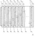
도 1은 본 발명에 관한 제 1 실시형태의 다층 배선 기판(1)의 적층 구조를 개략적으로 나타내는 도면이다. 도 1에 나타내는 바와 같이, 다층 배선 기판(1)은 세퍼레이터(121, ..., 12N-1)를 사이에 두고 적층된 수지 기재(101, ..., 10N)와 이들 수지 기재(101, ..., 10N)의 한쪽 면에 각각 형성된 배선 패턴(111, ..., 11N)과, 이들 배선 패턴(111~11N)을 전기적으로 접속하는 도전성 범프(201, 212, ..., 20N-1)를 포함하는 것이다.Fig. 1 schematically shows a lamination structure of a
도전성 범프(201~20N-1)는 수지 기재(101~10N) 및 세퍼레이터(121~12N-1)를 관통하도록 형성되어 있다. 즉, 각층의 도전성 범프(20k)(k는 1 ~ N-1 중 어느 하나)는 서로 이웃하는 배선 패턴(11k, 11k+1) 중 한쪽의 배선 패턴(11k)으로부터 다른 쪽의 배선 패턴(11k+1)으로 돌기하도록 형성되어 있다.The
도전성 범프(201~20N-1)의 구성 재료는 금, 은, 니켈, 주석, 납, 아연, 비스무트, 안티몬 및 구리로 이루어진 군으로부터 선택된 1종 또는 2종 이상의 금속 재료이면 된다.The constituent material of the
배선 패턴(111~11N) 및 도전성 범프(201~20N-1)에 의해 고주파 수동 소자를 구성할 수 있다. 고주파 수동 소자로는 예를 들어, 저항기, 인덕터, 캐패시터 혹은 코일 안테나 또는 이들의 조합을 들 수 있다.The high- frequency passive elements can be constituted by the
세퍼레이터(121~12N-1)는 열가소성 수지 재료로 이루어지고, 수지 기재(101~10N)도 열가소성 수지 재료로 이루어진다. 수지 기재(101~10N)를 구성하는 열가소성 수지 재료는 세퍼레이터(121~12N-1)를 구성하는 열가소성 수지 재료의 유리 전이 온도 Tg1보다도 높은 유리 전이 온도 Tg2를 가지고 있다. 이와 같은 수지 기재(101~10N)와 세퍼레이터(121~12N-1)를 Tg1보다도 높고, 또한 Tg2 미만의 범위 내의 온도에서 열융착함으로써 다층 배선 기판(1)이 제작된다. 즉, 수지 기재(101~10N)를 용융 연화시키지 않고 세퍼레이터(121~12N-1)를 용융 연화시키는 온도에서 수지 기재(101~10N)와 세퍼레이터(121~12N-1)를 열융착시켜 일체화함으로써,열융착 공정에서 수지 기재(101~10N) 상의 배선 패턴(111~11N)의 형상이 변화되는 것을 방지하는 것이 가능하다.The
수지 기재(101~10N)의 열가소성 수지 재료와 세퍼레이터(121~12N-1)의 열가소성 수지 재료는 각각 서로 상이한 유리 전이 온도 Tg2, Tg1를 가지는 환상 올레핀계 수지 조성물을 주성분으로 하여 구성되어 있다. 환상 올레핀계 수지는 환상 올레핀 모노머의 (공)중합체를 주체로서 포함한다. 중합 조건을 바꿈으로써 환상 올레핀계 수지의 분자량이나 가교 밀도를 제어해 원하는 유리 전이 온도 Tg2, Tg1를 얻는 것이 가능하다. 중합도를 높게 하거나 환상 올레핀계 수지가 가지는 측쇄를 길게 하거나 함으로써 유리 전이 온도 Tg2, Tg1를 높게 할 수 있다.The thermoplastic resin material of the resin substrate (101 to 10N ) and the thermoplastic resin material of the separators (121 to 12N-1 ) are constituted by using as a main component a cyclic olefin resin composition having glass
고주파 영역에서의 뛰어난 전기 특성(저유전 탄젠트, 저유전율)을 얻는 관점에서는 환상 올레핀계 수지 조성물 중에서도 특히 노르보넨계 수지가 바람직하다. 노르보넨계 수지는 10GHz에서 유전율이 약 2, 유전 탄젠트가 10-3~10-4오더라는 전기 특성을 실현할 수 있다. 예를 들어, 10GHz에서 유전율이 약 2, 유전 탄젠트가 10-4오더라는 전기 특성을 가지는 노르보넨계 수지로서 TiCoNa사제의 상품명「TOPAS 8007」(유리 전이 온도 78℃), 「TOPAS 6013」(유리 전이 온도 138℃), 「TOPAS 6015」(유리 전이 온도 158℃), 「TOPAS 5013」(유리 전이 온도 134℃), 「TOPAS 6017」(유리 전이 온도 178℃)이 시판되고 있다.From the standpoint of obtaining excellent electrical properties (low dielectric tangent, low dielectric constant) in the high frequency range, norbornene-based resins are particularly preferable among the cyclic olefin resin compositions. The norbornene resin can realize an electric characteristic that the dielectric constant is about 2 at 10 GHz and the dielectric tangent is about 10-3 to 10-4 . TOPAS 8007 " (glass transition temperature: 78 占 폚) and TOPAS 6013 (trade name, manufactured by TiCoNa) having electrical properties such that the dielectric constant is about 2 and the dielectric tangent is 10-4 at 10 GHz, TOPAS 6015 " (glass transition temperature 158 DEG C), TOPAS 5013 (glass transition temperature 134 DEG C), and TOPAS 6017 (glass transition temperature 178 DEG C).
열융착 공정에 있어서, 수지 기재(101~10N)를 용융 연화시키지 않고 세퍼레이터(121~12N-1)의 용융 연화를 일으키게 하기 위해서는 수지 기재(101~10N)와 세퍼레이터(121~12N-1) 사이의 유리 전이 온도의 차이(= Tg2 - Tg1)가 약 50℃인 것이 바람직하다. 예를 들어, 수지 기재(101~10N)와 세퍼레이터(121~12N-1)의 조합으로서 「TOPAS 5013」과 「TOPAS 8007」의 조합을 들 수 있지만, 이것으로 한정되는 것은 아니다.In order to cause the softening and softening of the
다음에, 다층 배선 기판(1)의 바람직한 제조 공정에 대해서 설명한다.Next, a preferable manufacturing process of the
먼저, N개의 수지 기재(101~10N)의 한쪽 면에 각각 구리박을 형성한다. 다음에, N개의 수지 기재(101~10N) 중의 수지 기재(101~10N-1)에 각각 도전성 범프(201~20N-1)를 매립 형성한다. 구체적으로는 수지 기재(101~10N-1)의 다른 쪽 면으로부터 각각 구리박에 이르는 관통공을 형성한다. 계속해서 전해 도금법 또는 페이스트 인쇄 넣기법에 의해 이들 관통공의 내부로부터 각각 외부로 돌출하는 도전성 돌기부를 형성한다. 도전성 돌기부는 예를 들어, 구리로 구성하면 된다. 또, 레이저를 사용하면 수지 기재(101~10N-1)에 고정밀도의 관통공을 용이하게 형성할 수 있다. 다음에, 도전성 돌기부의 노출면을 금속 또는 합금으로 피복한다. 금속으로는 금, 은, 니켈, 주석, 납, 아연, 비스무트 및 안티몬으로 이루어진 군으로부터 선택된 적어도 1종으로 이루어지고, 단층 또는 2층 이상이어도 된다. 합금으로는 주석, 납, 은, 아연, 비스무트, 안티몬 및 구리로 이루어진 군으로부터 선택된 적어도 2종 이상의 금속으로 구성된 납땜을 들 수 있다. 납땜으로는 예를 들어, 주석-납계, 주석-은계, 주석-아연계, 주석-비스무트계, 주석-안티몬계, 주석-은-비스무트계 혹은 주석-구리계를 들 수 있지만, 이것들로 한정되지 않고 최적인 것을 선택하면 된다. 당연, 여기서 든 금속 또는 합금의 융점은 수지 기재(101~10N) 또는 세퍼레이터(121~12N-1)의 유리 전이 온도보다 충분히 높아 상기 열융착 공정에서 융해하지 않는다.First, a copper foil is formed on one side of each of theN
다음에, N개의 수지 기재(101~10N)의 면 위에 형성된 구리박을 에칭해 배선 패턴(111~11N)을 형성한다. 이들 배선 패턴(111~11N)은 예를 들어, 인덕터, 저항기, 캐패시터 혹은 정합 회로 등의 고주파 수동 소자를 구성하도록 미리 설계된 것이다. 또한, 이 공정에서 형성되는 배선 패턴(111~11N) 중 적어도 일부는 주회(周回) 각도가 360°를 넘는 소용돌이 모양의 배선 패턴으로 하는 것이 바람직하다. 그 상세한 내용에 대해서는 후술한다.Next, the copper foils formed on the surfaces of theN
다음에, 도 2에 나타내는 바와 같이 성형기 내에서 수지 기재(101, ..., 10N)를 세퍼레이터(121, ..., 12N-1)를 사이에 두고 서로 포갠다. 이때, 배선 패턴(111~11N)이 모두 동일 방향을 향하도록 수지 기재(101~10N)는 배치되고, 도전성 범프가 형성되어 있지 않은 수지 기재(10N)는 가장 외측에 배치된다.Next, as shown in Fig. 2, the
다음에, 성형기 내에 배치된 수지 기재(101~10N) 및 세퍼레이터(121~12N-1)를 세퍼레이터(121~12N-1)의 유리 전이 온도 Tg1보다도 높고, 또한 수지 기재(101~10N)의 유리 전이 온도 Tg2 미만의 범위 내의 온도에서 열압한다. 이에 의해, 수지 기재(101~10N) 및 세퍼레이터(121~12N-1)가 열융착된다. 도전성 범프(201, ..., 20N-1)는 각각 용융 연화된 세퍼레이터(121, ..., 12N-1)를 관통하여 배선 패턴(112, ..., 11N)의 표면과 접합된다.Next, the
도 3(A) 및 도 3(B)는 인덕터 또는 코일 안테나용의 나선 모양 배선을 구성하는 배선 패턴(11k,11m)의 예를 개략적으로 나타내는 평면도이다. 도 3(A)의 배선 패턴(11k)과 도 3(B)의 배선 패턴(11m) 조합으로 나선 모양 배선을 구성할 수 있다. 도 3(A)의 배선 패턴(11k)은 단부에 범프 접합점(21k,22k)을 가지는 소용돌이 모양 배선으로서 그 주회 각도는 거의 360°이다. 도 3(B)의 배선 패턴(11m)은 단부에 범프 접합점(21m,22m)을 가지는 소용돌이 모양 배선으로서 그 주회 각도는 360°를 넘고 있다. 또한, 도 3에 있어서, 배선 패턴(11k,11m)은 곡선과 직선의 조합으로 이루어진 형상이지만, 곡선만으로 구성되어도 되고, 직선만으로 구성되어도 된다.Figure 3 (A) and 3 (B) is a plan view schematically showing an example of a wiring pattern (11k, 11m) constituting a spiral-shaped wire for the inductor or coil antenna. FIG wiring pattern (11k) of 3 (A) and can form a wiring pattern (11m) a spiral-shaped wiring by the combination of Fig. 3 (B). FIG wiring pattern (11k) is a spiral-shaped wire having a bump junction (21k, 22k) at the ends of the main angle 3 (A) is substantially 360 °. The
여기서, 나선 모양이란 다층 배선 기판(1)의 두께 방향으로 회전하면서 상승 또는 하강하는 형상을 말한다. 또, 소용돌이 모양이란 다층 배선 기판(1)의 평면상에서 선회함에 따라 중심축으로부터 멀어지는 또는 가까워지는 형상을 말한다.Here, the spiral shape refers to a shape that rises or falls while rotating in the thickness direction of the
도 3(A)의 배선 패턴(11k)의 일단에 형성되는 범프 접합점(22k)과 도 3(B)의 배선 패턴(11m)의 일단에 형성되는 범프 접합점(22m)을 도전성 범프를 통해 접속함으로써 나선 모양 배선을 형성할 수 있다. 혹은 도 3(A)의 배선 패턴(11k)의타단에 형성되는 범프 접합점(21k)과 도 3(B)의 배선 패턴(11m) 타단에 형성되는 범프 접합점(21m)을 도전성 범프를 통해 접속함으로써 나선 모양 배선을 형성하는 것이 가능하다.Once bump junction (22k) and one bump junction (22m) formed on the wiring pattern (11m) of Figure 3 (B) formed on the wiring pattern (11k) of Figure 3 (A) the conductive bump So that spiral wiring can be formed. Or of the wiring pattern (11k) of Figure 3 (A) The bump junction (21k) and the bump junction (21m) formed on the wiring pattern (11m) the other end of FIG. 3 (B) formed on the other end it is possible to form a spiral-shaped line, by connecting via the conductive bump.
도 4는 도 3(A), (B)의 배선 패턴(11k,11m)을 이용해 형성된 나선 모양 배선을 나타내는 개략도이다. 홀수번째 층의 배선 패턴(111, 113, ..., 11N-1)(여기서, N은 짝수)은 도 3(A)의 배선 패턴(11k)과 동일한 형상을 가지고 있고, 짝수번째 층의 배선 패턴(112, 114, ..., 11N)는 도 3(B)의 배선 패턴(11m)과 동일한 형상을 가지고 있다. 그리고, 이들 배선 패턴(111~11N)은 도전성 범프(201~20N-1)에 의해 형성되는 층간 접속 라인(231~23N-1)을 통해 전기적으로 접속되어 있다.Figure 4 is a schematic view showing a spiral wire formed with a wiring pattern (11k, 11m) of Figure 3 (A), (B) . The odd-numbered
상기 제 1 실시형태의 다층 배선 기판(1) 및 그 제조 방법이 나타내는 효과는 다음과 같다.The effects of the
다층 배선 기판(1)의 제조 공정에서는 표면에 배선 패턴(111~11N)이 형성된 수지 기재(101~10N)와 세퍼레이터(121~12N-1)를 열융착할 때에 세퍼레이터(121~12N-1)의 유리 전이 온도 Tg1보다도 높고, 수지 기재(101~10N)의 유리 전이 온도 Tg2 미만의 온도에서 수지 기재(101~10N)와 세퍼레이터(121~12N-1)를 열융착시키므로, 수지 기재(101~10N)의 열가소성 수지를 용융 연화시키지 않고 세퍼레이터(121~12N-1)의 열가소성 수지를 용융 연화시킬 수 있다. 이 상태로, 세퍼레이터(121~12N-1)와 수지(101~10N)를 열압하므로 용융 연화하지 않는 수지 기재(101~10N)에 형성된 도전성 범프(201, ..., 20N-1)는 각각 용융 연화된 세퍼레이터(121, ..., 12N-1)를 관통하여 배선 패턴(112, ..., 11N)의 표면과 접합된다. 따라서, 열융착 공정에서의배선 패턴(111~11N)의 형상 변화를 방지할 수 있다.In the manufacturing process of the
따라서, 고주파 대역에서 뛰어난 전기 특성(저유전율이나 저유전 손실)을 가져 형상 정밀도가 양호한 배선 패턴(111~11N)을 가지는 다층 배선 기판(1)을 제공할 수 있다.Therefore, it is possible to provide the
또, 짝수번째 층의 배선 패턴(112, 114, ..., 11N)는 주회 각도가 360°를넘고 있어 그 상하에 구성되는 홀수번째 층의 배선 패턴(111, 113, ..., 11N-1)과 대향하는 부분은 거의 원형으로 할 수 있다. 만일, 배선 패턴(111~11N)의 주회 각도가 360°미만이면 주회 각도가 360°에 미치지 않는 쪽의 턴수가 줄어들게 되어 나선 모양 배선의 인덕턴스가 감소된다. 즉, 본 실시형태의 나선 모양 배선은 인덕턴스를 해치지 않고 형성할 수 있다.In the even-numbered
(제 2 실시형태)(Second Embodiment)
다음에, 본 발명에 관한 제 2 실시형태에 대해서 설명한다. 도 5는 제 2 실시형태의 다층 배선 기판(2)의 적층 구조를 개략적으로 나타내는 도면이다. 도 6은 다층 배선 기판(2) 내에 형성된 나선 모양 배선을 구성하는 배선 패턴(111~1117)의 일례를 나타내는 개략도이다. 제 2 실시형태의 다층 배선 기판(2)은 도전성 범프(201~2016)의 위치와 배선 패턴(111~1117)의 형상을 제외하고 상기 제 1 실시형태의 다층 배선 기판(1)과 동일한 구성을 갖고, 제 1 실시형태의 다층 배선 기판(1)과 동일한 공정으로 제조되는 것이다.Next, a second embodiment of the present invention will be described. 5 is a view schematically showing the lamination structure of the
배선 패턴(111~1117)은 각각 주회 각도가 360°를 넘는 소용돌이 모양의 배선 패턴이다. 홀수번째 층의 수지 기재(101, 103, ..., 1017) 상에 형성되는 배선 패턴(111, 113, ..., 1117)과 짝수번째 층의 수지 기재(102, 104, ..., 1016) 상에 형성되는 배선 패턴(112, 114, ..., 1116)은 한쪽을 반전시킨 형상으로 되어 있다. 즉, 수지 기재(101, 103, ..., 1017)와 수지 기재(102, 104, ..., 1016)는 교대로 배치되므로, 배선 패턴(111~1117)은 표리 교대로 서로 포개어진다. 당연히 배선 패턴(111~1117)은 각각의 단부끼리가 도전성 범프를 통해 접속되어 있다.The
제 1 실시형태에서는 도 1 및 도 4에 나타낸 바와 같이, 홀수번째 층의 도전성 범프(201, 203, ..., 20N-1)(여기서, N은 짝수)는 적층 방향으로부터 봐서 서로 중복되는 위치에 형성되어 있고, 짝수번째 층의 도전성 범프(202, 204, ..., 20N-2)도 적층 방향으로부터 봐서 서로 중복되는 위치에 형성되어 있다. 그러므로, 제 1 실시형태의 다층 배선 구조에서는 사용되는 열가소성 수지의 종류나 열압 조건에 따라서는 두께가 불균일하게 되는 경우가 있다.In the first embodiment, as shown in Figs. 1 and 4, the
이와는 대조적으로, 제 2 실시형태에서는 배선 패턴(111~1117)을 표리 교대로 서로 포개어져 있으므로, 도전성 범프(201~2016)가 적층 방향으로부터 봤을 때에 서로 중복되지 않는 위치에 형성되어 있다. 또한, 도전성 범프(201~2016)를 매립한 수지 기재(101~1016)는 16층이므로, 배선 패턴(111~1117)의 주회 각도를 (360°+ 360°/16)로 하여 형성함으로써, 배선 패턴(111~1117) 중심축의 주위에 균등한 각도 간격으로 층간 접속 라인(231~2316)을 배치할 수 있다. 즉, 도 6에 나타내는 바와같이, 배선 패턴(111~1117)은 도전성 범프(201~2016)에 의해 형성되는 층간 접속 라인(231~2316)을 통해 전기적으로 접속되어 있다. 층간 접속 라인(231~2316)은 배선 패턴(111~1117)의 중심축 주위에 약 22.5°의 각도 간격으로 배치되어 있다.In contrast, in the second embodiment, since the
상기와 같이, 제 2 실시형태의 다층 배선 기판(2)의 도전성 범프(201~2016)는 적층 방향으로부터 봤을 때에 서로 중복되지 않는 위치에 형성되어 있으므로 두께의 불균일을 회피할 수 있다. 이에 의해, 다층 배선 기판(2)의 강성 밸런스가 좋아져 강도가 향상된다.As described above, since the
또한, 제 2 실시형태의 다층 배선 기판(2)의 층수는 17층이지만 이것으로 한정되지 않고, 18층 이상의 층수를 가지도록 다층 배선 기판(2)을 변형시켜도 된다. 예를 들면, 다층 배선 기판(2)의 층의 수가 N인 경우 도전성 범프(20)를 매립한 수지 기재(10)의 수는 N-1이며, 배선 패턴(11)의 주회 각도를 (360°+ 360°/(N-1))로 하여 형성함으로써, 배선 패턴(11)의 중심축 주위에 균등한 각도 간격으로 층간 접속 라인(23)을 배치할 수 있다.The
제 2 실시형태의 변형예로서 도 7에 나타내는 바와 같은 나선 모양 배선을 가지는 다층 배선 기판도 있을 수 있다. 도 7에 나타내는 바와 같이, 홀수번째 층간 접속 라인(231, 233, 235, 237)은 배선 패턴(111~118)의 중심축 주위에 약 45°의 각도 간격으로 배치되도록 형성되어 있고, 짝수번째 층간 접속 라인(232, 234, 236)은 배선 패턴(111~118)의 중심축 주위에 균등한 각도 간격으로 배치되도록 형성되어 있다.As a modification of the second embodiment, there may be a multilayer wiring board having a spiral wiring as shown in Fig. 7, the odd-numbered
이상, 도면을 참조해 본 발명의 실시형태에 대해서 설명했지만, 이것들은 본 발명의 예시이며 상기 이외의 여러가지 구성을 채용할 수도 있다. 예를 들어, 상기 제 1 및 제 2 실시형태는 모두 6층 이상의 배선 패턴을 가지고 있었지만, 이것으로 한정되는 것은 아니다. 제 1 실시형태의 변형예로서 적어도 2층의 배선 패턴을 가지는 다층 배선 기판의 형태가, 제 2 실시형태의 변형예로서 적어도 2층의 배선 패턴을 가지는 다층 배선 기판의 형태가 각각 존재할 수 있다.Although the embodiments of the present invention have been described with reference to the drawings, they are examples of the present invention and various configurations other than the above may be employed. For example, although the first and second embodiments have six or more wiring patterns, the present invention is not limited thereto. As a modification of the first embodiment, a multilayer wiring board having at least two wiring patterns and a multilayer wiring board having at least two wiring patterns as a modification of the second embodiment may be respectively present.
또, 인덕터를 실현하는 배선은 도 4 및 도 6에 나타낸 바와 같이, 복수의 소용돌이 모양의 배선 패턴을 나선 모양으로 접속함으로써 형성하면 되지만, 배선 패턴의 형상은 이것들로 한정되는 것은 아니다. 그 형상은 원호상이어도 방형상이어도 다각형상이라도 된다.The wiring for realizing the inductor may be formed by connecting a plurality of spiral-shaped wiring patterns in a spiral shape as shown in Figs. 4 and 6, but the shape of the wiring pattern is not limited to these. The shape thereof may be circular, rectangular or polygonal.
또한, 본 발명의 다층 배선 기판은 상술한 배선 패턴을 형성하는 수지 기재의 층이나 세퍼레이터의 층 이외의 층을 본 발명의 특징에 모순되지 않는 범위에서 구비해도 상관없다.
The multilayer wiring board of the present invention may be provided with layers other than the resin-based layer or the separator layer for forming the above-described wiring pattern within a range inconsistent with the features of the present invention.
본 출원은 일본 특허청에 출원된 특원 2008-279732호(출원일: 2008년 10월 30일)를 기초로 하는 우선권을 주장하는 것으로, 그 개시된 모두는 본 명세서의 일부로서 원용(incorporation herein by reference)된다.This application claims priority based on Japanese Patent Application No. 2008-279732 (filed on October 30, 2008), the disclosure of which is incorporated herein by reference in its entirety .
Claims (20)
Translated fromKorean상기 복수의 수지 기재의 한쪽 면에 각각 형성된 복수의 배선 패턴
을 포함하되,
상기 복수의 배선 패턴의 각각은 곡선 형상을 가지며, 상기 복수의 배선 패턴의 제 1 패턴이 제 1 수지 기재 상에 형성되고, 상기 복수의 배선 패턴의 제 2 패턴이 제 2 수지 기재 상에 형성되고, 상기 제 1 패턴은 제 1 접합단과 제 2 접합단을 가지며, 상기 제 2 패턴은 제 3 접합단과 제 4 접합단을 가지며,
상기 수지 기재 및 상기 세퍼레이터를 관통하도록 형성되고, 상기 복수의 배선 패턴을 전기적으로 접속하는 복수의 도전성 범프를 더 포함하며,
제 1 도전성 범프가 상기 제 2 접합단을 상기 제 3 접합단에 전기적으로 접속하고, 상기 제 4 접합단이 상기 제 1 접합단에 겹치지만, 상기 제 1 접합단과의 사이의 세퍼레이터에 의해 상기 제 1 접합단과 이간하도록 상기 복수의 배선 패턴이 전기적으로 접속되고, 상기 제 1 패턴과 상기 제 2 패턴은 상기 제 1 도전성 범프를 사이에 두고 전체적으로 나선 모양을 형성하고 있으며,
상기 수지 기재 및 상기 세퍼레이터는 열융착되어 있으며,
상기 세퍼레이터는 제 1 유리 전이 온도를 가지는 제 1 열가소성 수지 재료로 이루어지고,
상기 각 수지 기재는 상기 제 1 유리 전이 온도보다도 높은 제 2 유리 전이 온도를 가지는 제 2 열가소성 수지 재료로 이루어진 다층 배선 기판.A plurality of resin substrates stacked with a separator therebetween,
A plurality of wiring patterns formed on one surface of each of the plurality of resin substrates
≪ / RTI >
Wherein each of the plurality of wiring patterns has a curved shape, a first pattern of the plurality of wiring patterns is formed on the first resin base, a second pattern of the plurality of wiring patterns is formed on the second resin base material Wherein the first pattern has a first bonding end and a second bonding end, the second pattern has a third bonding end and a fourth bonding end,
Further comprising a plurality of conductive bumps formed to penetrate the resin base material and the separator and electrically connecting the plurality of wiring patterns,
The first conductive bump electrically connects the second junction node to the third junction node, and the fourth junction node overlaps with the first junction node, but the separator between the first junction node and the first junction node electrically connects the second junction node to the third junction node, And the first pattern and the second pattern form a spiral shape as a whole with the first conductive bump therebetween,
The resin base material and the separator are thermally fused,
Wherein the separator is made of a first thermoplastic resin material having a first glass transition temperature,
Wherein each of the resin substrates comprises a second thermoplastic resin material having a second glass transition temperature higher than the first glass transition temperature.
상기 제 1 도전성 범프는 상기 배선 패턴 중 상기 제 1 패턴의 상기 제 2 접합단으로부터 상기 제 2 패턴의 상기 제 3 접합단으로 돌기하도록 형성되어 있는 다층 배선 기판.The method according to claim 1,
Wherein the first conductive bump is formed so as to protrude from the second bonding end of the first pattern to the third bonding end of the second pattern among the wiring patterns.
상기 제 1 및 제 2 열가소성 수지 재료는 각각 서로 상이한 유리 전이 온도를 가지는 환상 올레핀계 수지 조성물을 주성분으로 하여 구성되어 있는 다층 배선 기판.The method according to claim 1 or 2,
Wherein the first and second thermoplastic resin materials each comprise a cycloolefin resin composition having a glass transition temperature different from each other as a main component.
상기 환상 올레핀계 수지 조성물은 노르보넨계 수지인 다층 배선 기판.The method of claim 3,
Wherein the cycloolefin resin composition is a norbornene resin.
상기 도전성 범프는 금, 은, 니켈, 주석, 납, 아연, 비스무트, 안티몬 및 구리로 이루어진 군으로부터 선택된 1종 또는 2종 이상의 금속 재료로 이루어진 다층 배선 기판.The method according to claim 1,
Wherein the conductive bump is made of one or more metal materials selected from the group consisting of gold, silver, nickel, tin, lead, zinc, bismuth, antimony, and copper.
상기 복수의 배선 패턴 및 상기 도전성 범프는 수동 소자를 구성하고 있는 다층 배선 기판.The method according to claim 1,
Wherein the plurality of wiring patterns and the conductive bumps constitute passive elements.
상기 수동 소자는 저항기, 인덕터 및 캐패시터 중에서 선택된 1종 또는 복수종의 회로를 포함하는 다층 배선 기판.The method of claim 6,
Wherein the passive element includes at least one circuit selected from a resistor, an inductor, and a capacitor.
제 3 수지 기재 상에 형성된 상기 복수의 배선 패턴의 제 3 패턴을 더 구비하되,
상기 제 3 패턴은 제 5 접합단과 제 6 접합단을 가지며, 제 2 도전성 범프가 상기 제 4 접합단을 상기 제 5 접합단에 접속하고,
상기 제 1 및 제 2 도전성 범프는 적층 방향으로부터 봐서 서로 상이한 위치에 형성되어 있는 다층 배선 기판.The method according to claim 1,
And a third pattern of the plurality of wiring patterns formed on the third resin base material,
The third pattern has a fifth junction end and a sixth junction end, a second conductive bump connects the fourth junction end to the fifth junction end,
Wherein the first and second conductive bumps are formed at positions different from each other in the stacking direction.
상기 복수의 배선 패턴의 제 4 패턴이 제 4 수지 기재 상에 형성되고, 상기 제 4 패턴이 제 7 접합단과 제 8 접합단을 가지며, 제 3 도전성 범프가 상기 제 6 접합단을 상기 제 7 접합단에 접속하고 있는 다층 배선 기판.The method of claim 8,
A fourth pattern of the plurality of wiring patterns is formed on a fourth resin base material, the fourth pattern has a seventh bonding end and an eighth bonding end, and a third conductive bump forms the seventh bonding end, Layer wiring substrate.
상기 제 1 패턴, 상기 제 2 패턴 및 상기 제 3 패턴 중 적어도 하나는 주회(周回) 각도가 360°를 넘는 소용돌이 모양의 배선 패턴을 규정하는 다층 배선 기판.The method of claim 8,
Wherein at least one of the first pattern, the second pattern, and the third pattern defines a spiral-shaped wiring pattern having a circumference angle of more than 360 degrees.
상기 소용돌이 모양의 배선 패턴이 표리 교대로 서로 포개어지고, 또한 각각의 단부(端部)끼리가 상기 도전성 범프를 통해 접속되어 있는 다층 배선 기판.The method of claim 10,
Wherein the spiral-shaped wiring patterns are overlapped with each other in a front-to-back manner, and the respective end portions are connected to each other via the conductive bumps.
상기 도전성 범프가 매립된 상기 수지 기재의 수는 M개(M은 자연수)이며,
상기 소용돌이 모양의 배선 패턴의 주회 각도는 (360°+ 360°/M)인 다층 배선 기판.The method of claim 11,
The number of the resin substrates in which the conductive bumps are embedded is M (M is a natural number)
(360 DEG + 360 DEG / M) of the spiral-shaped wiring pattern.
상기 N개의 수지 기재의 한쪽 면에 각각 배선 패턴을 형성하는 공정
을 포함하되,
상기 복수의 배선 패턴의 각각은 곡선 형상을 가지며, 상기 복수의 배선 패턴의 제 1 패턴이 제 1 수지 기재 상에 형성되고, 상기 복수의 배선 패턴의 제 2 패턴이 제 2 수지 기재 상에 형성되고, 상기 제 1 패턴은 제 1 접합단과 제 2 접합단을 가지며, 상기 제 2 패턴은 제 3 접합단과 제 4 접합단을 갖도록 상기 배선 패턴이 형성되고,
상기 N개의 수지 기재를 세퍼레이터를 사이에 두고 서로 포개는 것과 아울러 상기 N개의 수지 기재 중 상기 도전성 범프가 매립 형성되어 있지 않은 수지 기재를 가장 외측에 배치하는 공정과,
상기 N개의 수지 기재가 세퍼레이터를 사이에 두고 서로 포개어진 후에, 상기 N개의 수지 기재 및 상기 세퍼레이터를 열융착시켜 일체화함으로써 상기 도전성 범프를 통해 상기 복수의 배선 패턴을 전기적으로 접속시키는 공정
을 더 포함하며,
제 1 도전성 범프가 상기 제 2 접합단을 상기 제 3 접합단에 접속하고, 상기 제 4 접합단이 상기 제 1 접합단에 겹치지만, 상기 제 1 접합단과의 사이의 세퍼레이터에 의해 상기 제 1 접합단과 이간하도록, 또한 상기 제 1 패턴과 상기 제 2 패턴은 상기 제 1 도전성 범프를 사이에 두고 전체적으로 나선 모양을 형성하도록 상기 복수의 배선 패턴이 전기적으로 접속되며,
상기 세퍼레이터는 제 1 유리 전이 온도를 가지는 제 1 열가소성 수지 재료로 이루어지고,
상기 각 수지 기재는 상기 제 1 유리 전이 온도보다도 높은 제 2 유리 전이 온도를 가지는 제 2 열가소성 수지 재료로 이루어지며,
상기 N개의 수지 기재 및 상기 세퍼레이터를 열융착시키는 공정에서는 상기 N개의 수지 기재 및 상기 세퍼레이터는 상기 제 1 유리 전이 온도보다도 높고 상기 제 2 유리 전이 온도 미만의 온도에서 열융착되는 다층 배선 기판의 제조 방법.A step of embedding conductive bumps in each of N-1 resin bases among N resin bases (N is an integer of 2 or more)
A step of forming a wiring pattern on one side of each of the N resin substrates
≪ / RTI >
Wherein each of the plurality of wiring patterns has a curved shape, a first pattern of the plurality of wiring patterns is formed on the first resin base, a second pattern of the plurality of wiring patterns is formed on the second resin base material , The first pattern has a first bonding end and a second bonding end, and the second pattern has the wiring pattern formed to have a third bonding end and a fourth bonding end,
A step of arranging the N resin base materials over each other with a separator interposed therebetween and a resin base material in which the conductive bumps are not buried among the N resin base materials,
A step of electrically connecting the plurality of wiring patterns through the conductive bumps by thermally fusing the N resin base material and the separator after the N resin base materials are superposed on each other with the separator interposed therebetween;
Further comprising:
The first conductive bump connects the second junction end to the third junction node and the fourth junction node overlaps with the first junction node but the first junction node is connected to the first junction node by the separator between the first junction node and the first junction node, The plurality of wiring patterns are electrically connected so that the first pattern and the second pattern form a spiral as a whole with the first conductive bump therebetween,
Wherein the separator is made of a first thermoplastic resin material having a first glass transition temperature,
Wherein each of the resin substrates is made of a second thermoplastic resin material having a second glass transition temperature higher than the first glass transition temperature,
Wherein the N resin base material and the separator are thermally fused at a temperature higher than the first glass transition temperature and lower than the second glass transition temperature in a step of thermally fusing the N resin base material and the separator .
상기 도전성 범프를 매립 형성하는 공정에서는 상기 제 1 도전성 범프는 상기 N-1개의 수지 기재 중 상기 제 1 수지 기재의 면으로부터 제 2 수지 기재의 면의 방향으로 돌기하도록 형성되는 다층 배선 기판의 제조 방법.14. The method of claim 13,
In the step of embedding the conductive bump, the first conductive bump is formed so as to protrude in the direction of the surface of the second resin base material from the surface of the first resin base material among the N-1 resin base materials .
상기 제 1 및 제 2 열가소성 수지 재료는 각각 서로 상이한 유리 전이 온도를 가지는 환상 올레핀계 수지 조성물을 주성분으로 하여 구성되어 있는 다층 배선 기판의 제조 방법.The method according to claim 13 or 14,
Wherein the first and second thermoplastic resin materials each comprise a cycloolefin resin composition having a glass transition temperature different from each other as a main component.
상기 환상 올레핀계 수지 조성물은 노르보넨계 수지인 다층 배선 기판의 제조 방법.16. The method of claim 15,
Wherein the cyclic olefin resin composition is a norbornene resin.
상기 도전성 범프는 금, 은, 니켈, 주석, 납, 아연, 비스무트, 안티몬 및 구리로 이루어진 군으로부터 선택된 1종 또는 2종 이상의 금속 재료로 이루어진 다층 배선 기판의 제조 방법.14. The method of claim 13,
Wherein the conductive bump is made of one or more metal materials selected from the group consisting of gold, silver, nickel, tin, lead, zinc, bismuth, antimony, and copper.
상기 배선 패턴을 형성하는 공정에서는 상기 N개의 수지 기재 중 적어도 일부에 주회 각도가 360°이상인 소용돌이 모양의 배선 패턴을 형성하고,
상기 N개의 수지 기재 및 상기 세퍼레이터를 열융착시키는 공정에서는 상기 소용돌이 모양의 배선 패턴의 일단을 하나의 도전성 범프를 통해 하나의 배선 패턴에 접속시키고, 타단을 다른 도전성 범프를 통해 다른 배선 패턴에 접속시키는 다층 배선 기판의 제조 방법.14. The method of claim 13,
Wherein in the step of forming the wiring pattern, a spiral-shaped wiring pattern having a main winding angle of 360 degrees or more is formed on at least a part of the N resin substrates,
In the step of thermally fusing the N resin base material and the separator, one end of the spiral-shaped wiring pattern is connected to one wiring pattern through one conductive bump, and the other end is connected to another wiring pattern through another conductive bump A method of manufacturing a multilayer wiring board.
상기 배선 패턴을 형성하는 공정에서는 제 1 수지 기재에 상기 소용돌이 모양의 배선 패턴을 형성하고, 제 2 수지 기재에 상기 소용돌이 모양의 배선 패턴을 반전시킨 배선 패턴을 형성하며,
상기 수지 기재를 배치하는 공정에서는 상기 제 1 수지 기재와 상기 제 2 수지 기재를 교대로 반복해 배치하고,
상기 N개의 수지 기재 및 상기 세퍼레이터를 열융착시키는 공정에서는 상기 제 1 수지 기재의 배선 패턴의 단부와 상기 제 2 수지 기재의 배선 패턴의 단부를 상기 도전성 범프를 통해 접속시키는 다층 배선 기판의 제조 방법.19. The method of claim 18,
In the step of forming the wiring pattern, the spiral-shaped wiring pattern is formed on the first resin base material, and the wiring pattern in which the spiral-shaped wiring pattern is inverted is formed on the second resin base material,
In the step of arranging the resin base material, the first resin base material and the second resin base material are alternately and repeatedly arranged,
And the end portions of the wiring patterns of the first resin base material and the end portions of the wiring patterns of the second resin base material are connected through the conductive bumps in the step of thermally fusing the N resin base material and the separator.
상기 배선 패턴을 형성하는 공정에서는 상기 소용돌이 모양의 배선 패턴의 주회 각도를 (360°+ 360°/(N-1))로 하여 형성하는 다층 배선 기판의 제조 방법.The method of claim 19,
Wherein the step of forming the wiring pattern has the main angle of the spiral-shaped wiring pattern set to (360 deg. + 360 deg. / (N-1)).
Applications Claiming Priority (2)
| Application Number | Priority Date | Filing Date | Title |
|---|---|---|---|
| JP2008279732 | 2008-10-30 | ||
| JPJP-P-2008-279732 | 2008-10-30 |
Publications (2)
| Publication Number | Publication Date |
|---|---|
| KR20110076995A KR20110076995A (en) | 2011-07-06 |
| KR101562086B1true KR101562086B1 (en) | 2015-10-20 |
Family
ID=42128564
Family Applications (1)
| Application Number | Title | Priority Date | Filing Date |
|---|---|---|---|
| KR1020117011093AExpired - Fee RelatedKR101562086B1 (en) | 2008-10-30 | 2009-10-28 | Multilayer circuit board and method of manufacturing the same |
Country Status (7)
| Country | Link |
|---|---|
| US (1) | US8787030B2 (en) |
| EP (1) | EP2367407A1 (en) |
| JP (1) | JP4518214B2 (en) |
| KR (1) | KR101562086B1 (en) |
| CN (1) | CN102204421A (en) |
| TW (1) | TW201031293A (en) |
| WO (1) | WO2010050193A1 (en) |
Families Citing this family (8)
| Publication number | Priority date | Publication date | Assignee | Title |
|---|---|---|---|---|
| JP2012186440A (en)* | 2011-02-18 | 2012-09-27 | Ibiden Co Ltd | Inductor component, printed circuit board incorporating the component, and manufacturing method of the inductor component |
| US10051741B2 (en)* | 2013-11-06 | 2018-08-14 | Qualcomm Incorporated | Embedded layered inductor |
| WO2015129601A1 (en)* | 2014-02-27 | 2015-09-03 | 株式会社村田製作所 | Electromagnet production method, and electromagnet |
| US9832875B2 (en)* | 2014-07-07 | 2017-11-28 | Hamilton Sundstrand Corporation | Method for manufacturing layered electronic devices |
| JP6397374B2 (en)* | 2015-07-01 | 2018-09-26 | 日本電信電話株式会社 | amplifier |
| WO2018034162A1 (en)* | 2016-08-18 | 2018-02-22 | 株式会社村田製作所 | Multilayer substrate and manufacturing method therefor |
| JP7047713B2 (en)* | 2018-11-05 | 2022-04-05 | オムロン株式会社 | Robot arm and robot arm manufacturing method |
| CN111970810A (en)* | 2019-05-20 | 2020-11-20 | 庆鼎精密电子(淮安)有限公司 | Multilayer resin substrate and method for manufacturing same |
Citations (4)
| Publication number | Priority date | Publication date | Assignee | Title |
|---|---|---|---|---|
| JP2003218532A (en) | 2002-01-23 | 2003-07-31 | Sumitomo Bakelite Co Ltd | Multilayered wiring board, wiring board for manufacturing the same, and their manufacturing methods |
| JP2004186433A (en) | 2002-12-03 | 2004-07-02 | Sumitomo Bakelite Co Ltd | Wiring board and multilayer wiring board |
| US20050155792A1 (en) | 2002-02-22 | 2005-07-21 | Fujikura Ltd. | Multilayer wiring board, base for multilayer wiring board, printed wiring board and its manufacturing method |
| JP2006102753A (en) | 2004-09-30 | 2006-04-20 | Sumitomo Bakelite Co Ltd | Thermosetting flux, flux sheet, and multilayer printed circuit board |
Family Cites Families (9)
| Publication number | Priority date | Publication date | Assignee | Title |
|---|---|---|---|---|
| JPH1154934A (en) | 1997-06-06 | 1999-02-26 | Ibiden Co Ltd | Multilayered printed wiring board and its manufacture |
| JP4515477B2 (en)* | 2001-06-05 | 2010-07-28 | 大日本印刷株式会社 | Method for manufacturing wiring board with passive element |
| EP1265466A3 (en)* | 2001-06-05 | 2004-07-21 | Dai Nippon Printing Co., Ltd. | Method for fabrication wiring board provided with passive element and wiring board provided with passive element |
| JP2004031803A (en)* | 2002-06-27 | 2004-01-29 | Fujikura Ltd | Multilayer wiring board and base material for multilayer wiring board |
| JP2005340577A (en) | 2004-05-28 | 2005-12-08 | Matsushita Electric Ind Co Ltd | Multilayer printed circuit board |
| JP4515160B2 (en)* | 2004-06-11 | 2010-07-28 | 大日本印刷株式会社 | Wiring board with built-in capacitor, capacitor element with built-in wiring board |
| JP4996838B2 (en) | 2005-09-29 | 2012-08-08 | 三菱樹脂株式会社 | Multilayer wiring board |
| JP2007184388A (en)* | 2006-01-06 | 2007-07-19 | Sumitomo Bakelite Co Ltd | Printed wiring board and method of manufacturing same |
| JP2008103640A (en) | 2006-10-20 | 2008-05-01 | Ngk Spark Plug Co Ltd | Multilayer wiring board |
- 2009
- 2009-10-28KRKR1020117011093Apatent/KR101562086B1/ennot_activeExpired - Fee Related
- 2009-10-28EPEP09823306Apatent/EP2367407A1/ennot_activeWithdrawn
- 2009-10-28USUS13/124,751patent/US8787030B2/enactiveActive
- 2009-10-28WOPCT/JP2009/005684patent/WO2010050193A1/enactiveApplication Filing
- 2009-10-28CNCN200980143786XApatent/CN102204421A/enactivePending
- 2009-10-28JPJP2010507167Apatent/JP4518214B2/enactiveActive
- 2009-10-29TWTW098136644Apatent/TW201031293A/enunknown
Patent Citations (4)
| Publication number | Priority date | Publication date | Assignee | Title |
|---|---|---|---|---|
| JP2003218532A (en) | 2002-01-23 | 2003-07-31 | Sumitomo Bakelite Co Ltd | Multilayered wiring board, wiring board for manufacturing the same, and their manufacturing methods |
| US20050155792A1 (en) | 2002-02-22 | 2005-07-21 | Fujikura Ltd. | Multilayer wiring board, base for multilayer wiring board, printed wiring board and its manufacturing method |
| JP2004186433A (en) | 2002-12-03 | 2004-07-02 | Sumitomo Bakelite Co Ltd | Wiring board and multilayer wiring board |
| JP2006102753A (en) | 2004-09-30 | 2006-04-20 | Sumitomo Bakelite Co Ltd | Thermosetting flux, flux sheet, and multilayer printed circuit board |
Also Published As
| Publication number | Publication date |
|---|---|
| US20110211321A1 (en) | 2011-09-01 |
| KR20110076995A (en) | 2011-07-06 |
| JPWO2010050193A1 (en) | 2012-03-29 |
| CN102204421A (en) | 2011-09-28 |
| US8787030B2 (en) | 2014-07-22 |
| EP2367407A1 (en) | 2011-09-21 |
| JP4518214B2 (en) | 2010-08-04 |
| TW201031293A (en) | 2010-08-16 |
| WO2010050193A1 (en) | 2010-05-06 |
Similar Documents
| Publication | Publication Date | Title |
|---|---|---|
| KR101562086B1 (en) | Multilayer circuit board and method of manufacturing the same | |
| JP6642708B2 (en) | Electronic components, diaphragms and electronic equipment | |
| JP6213698B2 (en) | Multi-layer substrate with built-in coil and manufacturing method thereof | |
| KR102360532B1 (en) | Inductor and manufacturing method thereof | |
| CN1867225B (en) | Multilayer assembly and method of manufacturing the same | |
| US20030222340A1 (en) | Enhancement of current-carrying capacity of a multilayer circuit board | |
| KR102021296B1 (en) | Composite electronic component and resistor device | |
| JP4791244B2 (en) | Electronic component built-in substrate and manufacturing method thereof | |
| KR20030066360A (en) | Semiconductor device built-in multilayer wiring board and method of manufacturing same | |
| JP2008311426A (en) | Multilayer wiring board and method for manufacturing multilayer wiring board | |
| WO2015079941A1 (en) | Multilayer-substrate manufacturing method, multilayer substrate, and electromagnet | |
| KR102041097B1 (en) | Composite electronic component and resistor device | |
| JP5725152B2 (en) | Multi-layer substrate with built-in electric element and manufacturing method thereof | |
| US9960122B2 (en) | Composite device with substrate and mounted component | |
| US10096901B2 (en) | Coil module | |
| JP4285339B2 (en) | Circuit module and method of manufacturing circuit module | |
| CN105609231A (en) | Laminated inductor and manufacturing method therefor and lamination packaging assembly | |
| US10468183B2 (en) | Inductor and manufacturing method of the same | |
| JP4010919B2 (en) | Inductive element manufacturing method | |
| JP4065125B2 (en) | Component built-in module and manufacturing method thereof | |
| JPWO2014069107A1 (en) | Component built-in board and communication terminal device | |
| US11856713B2 (en) | Multilayer resin substrate and method of manufacturing multilayer resin substrate | |
| JP6232976B2 (en) | Multilayer substrate manufacturing method, multilayer substrate and electromagnet | |
| JP6070290B2 (en) | Resin multilayer part and manufacturing method thereof | |
| CN109712896A (en) | The manufacturing method of junction structure, electronic component module, electronic component unit and electronic component unit |
Legal Events
| Date | Code | Title | Description |
|---|---|---|---|
| PA0105 | International application | St.27 status event code:A-0-1-A10-A15-nap-PA0105 | |
| P11-X000 | Amendment of application requested | St.27 status event code:A-2-2-P10-P11-nap-X000 | |
| P13-X000 | Application amended | St.27 status event code:A-2-2-P10-P13-nap-X000 | |
| PG1501 | Laying open of application | St.27 status event code:A-1-1-Q10-Q12-nap-PG1501 | |
| N231 | Notification of change of applicant | ||
| PN2301 | Change of applicant | St.27 status event code:A-3-3-R10-R13-asn-PN2301 St.27 status event code:A-3-3-R10-R11-asn-PN2301 | |
| A201 | Request for examination | ||
| P11-X000 | Amendment of application requested | St.27 status event code:A-2-2-P10-P11-nap-X000 | |
| P13-X000 | Application amended | St.27 status event code:A-2-2-P10-P13-nap-X000 | |
| PA0201 | Request for examination | St.27 status event code:A-1-2-D10-D11-exm-PA0201 | |
| E902 | Notification of reason for refusal | ||
| PE0902 | Notice of grounds for rejection | St.27 status event code:A-1-2-D10-D21-exm-PE0902 | |
| P11-X000 | Amendment of application requested | St.27 status event code:A-2-2-P10-P11-nap-X000 | |
| P13-X000 | Application amended | St.27 status event code:A-2-2-P10-P13-nap-X000 | |
| E701 | Decision to grant or registration of patent right | ||
| PE0701 | Decision of registration | St.27 status event code:A-1-2-D10-D22-exm-PE0701 | |
| PR0701 | Registration of establishment | St.27 status event code:A-2-4-F10-F11-exm-PR0701 | |
| PR1002 | Payment of registration fee | St.27 status event code:A-2-2-U10-U12-oth-PR1002 Fee payment year number:1 | |
| PG1601 | Publication of registration | St.27 status event code:A-4-4-Q10-Q13-nap-PG1601 | |
| LAPS | Lapse due to unpaid annual fee | ||
| PC1903 | Unpaid annual fee | St.27 status event code:A-4-4-U10-U13-oth-PC1903 Not in force date:20181015 Payment event data comment text:Termination Category : DEFAULT_OF_REGISTRATION_FEE | |
| PC1903 | Unpaid annual fee | St.27 status event code:N-4-6-H10-H13-oth-PC1903 Ip right cessation event data comment text:Termination Category : DEFAULT_OF_REGISTRATION_FEE Not in force date:20181015 |