KR101559913B1 - Plasma dry etching apparatus - Google Patents
Plasma dry etching apparatusDownload PDFInfo
- Publication number
- KR101559913B1 KR101559913B1KR1020090057172AKR20090057172AKR101559913B1KR 101559913 B1KR101559913 B1KR 101559913B1KR 1020090057172 AKR1020090057172 AKR 1020090057172AKR 20090057172 AKR20090057172 AKR 20090057172AKR 101559913 B1KR101559913 B1KR 101559913B1
- Authority
- KR
- South Korea
- Prior art keywords
- ring
- edge
- wafer
- coolant
- pedestal
- Prior art date
- Legal status (The legal status is an assumption and is not a legal conclusion. Google has not performed a legal analysis and makes no representation as to the accuracy of the status listed.)
- Active
Links
Images


Classifications
- H—ELECTRICITY
- H01—ELECTRIC ELEMENTS
- H01J—ELECTRIC DISCHARGE TUBES OR DISCHARGE LAMPS
- H01J37/00—Discharge tubes with provision for introducing objects or material to be exposed to the discharge, e.g. for the purpose of examination or processing thereof
- H01J37/32—Gas-filled discharge tubes
- H01J37/32009—Arrangements for generation of plasma specially adapted for examination or treatment of objects, e.g. plasma sources
- H01J37/32082—Radio frequency generated discharge
- H01J37/32091—Radio frequency generated discharge the radio frequency energy being capacitively coupled to the plasma
- H—ELECTRICITY
- H01—ELECTRIC ELEMENTS
- H01J—ELECTRIC DISCHARGE TUBES OR DISCHARGE LAMPS
- H01J37/00—Discharge tubes with provision for introducing objects or material to be exposed to the discharge, e.g. for the purpose of examination or processing thereof
- H01J37/32—Gas-filled discharge tubes
- H01J37/32431—Constructional details of the reactor
- H01J37/32715—Workpiece holder
- H01J37/32724—Temperature
- H—ELECTRICITY
- H01—ELECTRIC ELEMENTS
- H01L—SEMICONDUCTOR DEVICES NOT COVERED BY CLASS H10
- H01L21/00—Processes or apparatus adapted for the manufacture or treatment of semiconductor or solid state devices or of parts thereof
- H01L21/02—Manufacture or treatment of semiconductor devices or of parts thereof
- H01L21/04—Manufacture or treatment of semiconductor devices or of parts thereof the devices having potential barriers, e.g. a PN junction, depletion layer or carrier concentration layer
- H01L21/18—Manufacture or treatment of semiconductor devices or of parts thereof the devices having potential barriers, e.g. a PN junction, depletion layer or carrier concentration layer the devices having semiconductor bodies comprising elements of Group IV of the Periodic Table or AIIIBV compounds with or without impurities, e.g. doping materials
- H01L21/30—Treatment of semiconductor bodies using processes or apparatus not provided for in groups H01L21/20 - H01L21/26
- H01L21/31—Treatment of semiconductor bodies using processes or apparatus not provided for in groups H01L21/20 - H01L21/26 to form insulating layers thereon, e.g. for masking or by using photolithographic techniques; After treatment of these layers; Selection of materials for these layers
- H01L21/3105—After-treatment
- H01L21/311—Etching the insulating layers by chemical or physical means
- H01L21/31105—Etching inorganic layers
- H01L21/31111—Etching inorganic layers by chemical means
- H01L21/31116—Etching inorganic layers by chemical means by dry-etching
- H—ELECTRICITY
- H01—ELECTRIC ELEMENTS
- H01L—SEMICONDUCTOR DEVICES NOT COVERED BY CLASS H10
- H01L21/00—Processes or apparatus adapted for the manufacture or treatment of semiconductor or solid state devices or of parts thereof
- H01L21/02—Manufacture or treatment of semiconductor devices or of parts thereof
- H01L21/04—Manufacture or treatment of semiconductor devices or of parts thereof the devices having potential barriers, e.g. a PN junction, depletion layer or carrier concentration layer
- H01L21/18—Manufacture or treatment of semiconductor devices or of parts thereof the devices having potential barriers, e.g. a PN junction, depletion layer or carrier concentration layer the devices having semiconductor bodies comprising elements of Group IV of the Periodic Table or AIIIBV compounds with or without impurities, e.g. doping materials
- H01L21/30—Treatment of semiconductor bodies using processes or apparatus not provided for in groups H01L21/20 - H01L21/26
- H01L21/31—Treatment of semiconductor bodies using processes or apparatus not provided for in groups H01L21/20 - H01L21/26 to form insulating layers thereon, e.g. for masking or by using photolithographic techniques; After treatment of these layers; Selection of materials for these layers
- H01L21/3205—Deposition of non-insulating-, e.g. conductive- or resistive-, layers on insulating layers; After-treatment of these layers
- H01L21/321—After treatment
- H01L21/3213—Physical or chemical etching of the layers, e.g. to produce a patterned layer from a pre-deposited extensive layer
- H01L21/32133—Physical or chemical etching of the layers, e.g. to produce a patterned layer from a pre-deposited extensive layer by chemical means only
- H01L21/32135—Physical or chemical etching of the layers, e.g. to produce a patterned layer from a pre-deposited extensive layer by chemical means only by vapour etching only
- H01L21/32136—Physical or chemical etching of the layers, e.g. to produce a patterned layer from a pre-deposited extensive layer by chemical means only by vapour etching only using plasmas
- H01L21/32137—Physical or chemical etching of the layers, e.g. to produce a patterned layer from a pre-deposited extensive layer by chemical means only by vapour etching only using plasmas of silicon-containing layers
Landscapes
- Physics & Mathematics (AREA)
- Engineering & Computer Science (AREA)
- Plasma & Fusion (AREA)
- Chemical & Material Sciences (AREA)
- Analytical Chemistry (AREA)
- Drying Of Semiconductors (AREA)
Abstract
Translated fromKoreanDescription
Translated fromKorean본 발명은 플라즈마 식각 공정 중에 웨이퍼의 최외곽 온도를 제어하는 플라즈마 건식 식각 장치에 관한 것으로, 더 자세하게는 라디칼 에치(Radical etch)가 진행되는 폴리 에치(Poly etch)의 경우 라디칼 에천트(Radical etchant)의 밀도(Density)가 높아지면, 폴리실리콘막의 건식 식각 속도가 빨라져서 바(Bar)의 임계 선폭(CD)이 작아지고, 폴리메릭 에치(Polymeric etch)가 진행되는 옥사이드 에치(Oxide etch)의 경우 폴리머(Polymer)의 밀도(Density)가 높아지면, 옥사이드막의 건식 식각 속도가 느려져서 바(Bar)의 임계 선폭(CD)이 커지는 웨이퍼 프로세스와 같이, 웨이퍼의 표면 온도가 식각 프로파일에 중요한 파라메터가 되는 점을 고려하여 웨이퍼와 이웃하는 에지 링에 웨이퍼의 표면 온도를 조절하는 냉온 수단을 구비하는 플라즈마 건식 식각 장치에 관한 것이다.BACKGROUND OF THE INVENTION 1. Field of the Invention The present invention relates to a plasma dry etching apparatus for controlling an outermost temperature of a wafer during a plasma etching process, more specifically, a radical etchant for a poly etch in which a radical etch proceeds, The etch rate of the polysilicon film is increased so that the critical line width CD of the bar becomes smaller and the oxide etch of the polymer etch progresses when the density of the polymer becomes higher. The surface temperature of the wafer becomes an important parameter for the etch profile like the wafer process in which the dry etch rate of the oxide film becomes slow and the critical line width (CD) of the bar becomes larger as the density of the polymer increases. And cooling means for adjusting the surface temperature of the wafer in the edge ring adjacent to the wafer in consideration of the temperature of the wafer.
또한 본 발명은, 웨이퍼의 중심과 주변에서 식각 속도를 제어하기 위하여 웨 이퍼를 직접 지지하는 ECS 페데스탈에 백 사이드용 냉각장치 및 가열장치를 구비하는 것은 물론이고, 웨이퍼의 최외곽에서 식각 속도는 백 사이드용 냉각장치 및 가열장치를 통해서는 제어되지 않기 때문에, 커플링 링에 상기 페데스탈과 독립적으로 에지용 냉각수단 및 가열수단을 구비하고, 페데스탈과 커플링 링 사이에 열 차폐막을 설치하여 커플링 링을 독립적으로 제어하는 플라즈마 건식 식각 장치에 관한 것이다.Further, the present invention is not limited to the ECS pedestal that directly supports the wafers to control the etching speed at the center and periphery of the wafer, but also includes a backside cooling device and a heating device, Side cooling device and the heating device. Therefore, the coupling ring is provided with cooling means for edge and heating means independently of the pedestal, and a heat shielding film is provided between the pedestal and the coupling ring, To a plasma dry etching apparatus.
반도체 소자의 제조 공정은, 소정의 식각 장치를 사용하여, 반도체 웨이퍼 상에 형성된 물질막을 식각하는 공정을 포함한다. 예를 들면, 절연막을 관통하는 콘택 홀을 형성하는 공정이 그것이다. 이러한 식각 장치는, 식각 방법을 기준으로 건식 식각 장치 또는 습식 식각 장치로 구분될 수 있다.A manufacturing process of a semiconductor device includes a process of etching a material film formed on a semiconductor wafer using a predetermined etching apparatus. For example, the step of forming a contact hole through the insulating film is a step. Such an etching apparatus can be classified into a dry etching apparatus or a wet etching apparatus based on the etching method.
상기 습식 식각 장치는, 복수의 웨이퍼를 한 번에 처리할 수 있는 장점이 있지만, 등방성의 식각 특성 때문에 언더 컷(under cut) 등의 문제점이 발생 된다. 예를 들면, 콘택 홀 형성을 위한 식각 공정 등에는 습식 식각 장치가 부적합하다.The wet etching apparatus has an advantage in that a plurality of wafers can be processed at a time, but problems such as undercuts occur due to isotropic etching characteristics. For example, a wet etching apparatus is not suitable for an etching process for forming a contact hole.
반면, 건식 식각 장치는, 플라즈마를 이용하여 물질막을 식각하는 장치로서, 이방성의 식각 특성을 갖는다. 이에 따라, 건식 식각 장치는, 라인 앤 스페이스의 형성 공정이나 콘택 홀의 형성 공정 등에 폭넓게 사용될 수 있다.On the other hand, a dry etching apparatus is an apparatus for etching a material film by using plasma, and has an anisotropic etching characteristic. Accordingly, the dry etching apparatus can be widely used for a line-and-space forming step and a contact hole forming step.
상기 건식 식각 장치는, 다시 물리적 건식 식각 장치와 화학적 건식 식각 장치로 구분될 수 있다. 상기 물리적 건식 식각 장치는 플라즈마 내에 형성된 이온을 전기장에 의해 가속하여 물질막에 충돌시키는 과정을 이용한다. 이에 따라, 물 리적 건식 식각 장치는, 우수한 이방성 식각 특성을 갖지만, 물질막 아래의 막에 대한 식각 선택비는 좋지 않는 단점이 있다. 반면, 화학적 건식 식각 장치는, 물질막을 상기 플라즈마 내에 형성된 라디칼과의 화학적 반을을 통해 식각한다. 이에 따라, 화학적 건식 식각 장치는 선택적 식각 특성은 우수하지만, 전술한 등방성의 식각 특성을 가질 수도 있다. 최근에는 물리적 및 화학적 건식 식각 장치들의 장점을 조합하여, 선택적 식각 특성과 이방적 식각 특성이 모두 우수한 이온 강화 플라즈마 식각 방법이 사용되기도 한다.The dry etching apparatus may be further divided into a physical dry etching apparatus and a chemical dry etching apparatus. The physical dry etching apparatus uses a process of accelerating ions formed in a plasma by an electric field to collide with a material film. Accordingly, the physical dry etching apparatus has excellent anisotropic etching characteristics, but has a disadvantage in that the etching selectivity ratio to the film below the material film is poor. On the other hand, a chemical dry etching apparatus etches a material film through a chemical barrier with a radical formed in the plasma. Accordingly, although the chemical dry etching apparatus has excellent selective etching characteristics, it may have the above-described isotropic etching characteristics. In recent years, ion enhanced plasma etching methods having both selective etching properties and anisotropic etching characteristics have been used in combination with the advantages of physical and chemical dry etching devices.
그러나, 이러한 건식 시각 장치에도 불구하고, 라인 앤 스페이스의 형성 공정이나 콘택 홀 형성 공정에서 바(Bar)의 임계 선폭이 일정하지 않거나 혹은 콘택 홀(Hole)이 오픈되지 않는(Not open) 식각 불량이 여전히 존재한다.However, in spite of such a dry visual device, in the process of forming a line-and-space or the process of forming a contact hole, the critical line width of the bar is not constant, or the etching defect in which the contact hole (not open) It still exists.
따라서, 본 발명은 상기한 바와 같은 종래 기술의 문제점을 해결하기 위하여 안출된 것으로, 본 발명의 목적은 웨이퍼 가장자리 부분에서 바(Bar)의 선폭이 일정하지 않거나 콘택 홀(Hole)이 오픈되지 않는 식각 불량으로 인하여 대략 5㎜ 안밖의 웨이퍼 최외곽 영역을 폐기해야 하는 경제적 손실이 뒤 따랐기 때문에, 에지 링에 냉각수단 및 가열수단을 더 구비함으로써, 웨이퍼의 최외곽 영역도 상품으로써 활용할 수 있는 플라즈마 건식 식각 장치를 제공하는 것이다.SUMMARY OF THE INVENTION Accordingly, it is an object of the present invention to provide an etching method and a manufacturing method thereof, in which the line width of a bar is not constant at an edge of a wafer, Since the edge ring is further provided with a cooling means and a heating means since an economic loss to dispose the outermost wafer area of about 5 mm due to defects has been followed by the edge ring, the outermost region of the wafer is also subjected to plasma dry etching Device.
본 발명의 다른 목적은 웨이퍼의 표면 온도가 플라즈마 식각 특성에서 중요한 파라메터가 되는 점을 적극 반영하여 웨이퍼의 표면 온도를 액티브하게 제어할 수 있는 플라즈마 건식 식각 장치를 제공하는 것이다.Another object of the present invention is to provide a plasma dry etching apparatus capable of actively controlling the surface temperature of a wafer by positively reflecting the fact that the surface temperature of the wafer becomes an important parameter in the plasma etching characteristic.
본 발명의 또 다른 목적은 웨이퍼를 직접 지지하는 페데스탈은 물론이고 웨이퍼와 소정 거리를 두고 이웃하는 에지 링의 온도를 독자적으로 제어할 수 있는 플라즈마 건식 식각 장치를 제공하는 것이다.It is another object of the present invention to provide a plasma dry etching apparatus capable of independently controlling the temperature of an edge ring adjacent to a wafer at a predetermined distance as well as a pedestal supporting the wafer directly.
본 발명의 또 다른 목적은 라디칼 에치가 진행되는 폴리 에치와, 폴리메릭 에치가 진행되는 옥사이드 에치와 같이, 프로세스 가스에 따라 식각 속도가 빨라지는 경우는 물론이고 식각 속도가 느려지는 경우에도 식각 제어를 선택적으로 수행할 수 있는 플라즈마 건식 식각 장치를 제공하는 것이다.It is another object of the present invention to provide an etching control method and a manufacturing method of a semiconductor device, which can be used not only in a case where the etch rate is increased according to a process gas, such as a polyetrix radical etchant, And to provide a plasma dry etching apparatus which can be selectively performed.
전술한 바와 같은 목적을 달성하기 위한 본 발명의 특징에 따르면, 본 발명 은 식각 공정이 수행되는 프로세스 챔버와, 상기 프로세스 챔버 내부에 구비되어 웨이퍼가 로딩되는 페데스탈과, 상기 프로세스 챔버 내부에 구비되어 고주파(RF) 전원을 인가하는 전극 캐소드 및 전극 플레이트과, 상기 페데스탈의 가장자리에 구비되는 에지 링과, 일측은 상기 페데스탈에 지지되고, 타측은 상기 에지 링과 연결되는 커플링 링과, 상기 커플링 링에 구비되고, 상기 웨이퍼 최외곽(Extreme edge) 온도의 상승(Raise) 혹은 하강(Drop)을 위하여, 상기 에지 링을 냉각(Cooling) 혹은 가열(Heating) 하는 에지용 냉각수단 및 가열수단을 포함한다.According to an aspect of the present invention, there is provided a plasma processing apparatus including a process chamber in which an etching process is performed, a pedestal provided in the process chamber and loaded with a wafer, An electrode cathode and an electrode plate for applying RF power to the edge ring, an edge ring provided at the edge of the pedestal, a coupling ring having one side supported by the pedestal and the other side connected to the edge ring, And includes an edge cooling means and a heating means for cooling or heating the edge ring in order to raise or lower the extreme edge temperature of the wafer.
상기 프로세스 챔버는, 프로세스 가스를 플라즈마화함으로써, 웨이퍼 상에 적층된 폴리실리콘막 혹은 옥사이드막을 패턴닝하거나 혹은 콘택 홀을 형성하는 건식 식각하는 장치이고, 상기 에지용 냉각수단은, 폴리 에치(Poly etch) 공정시 패턴의 임계 선폭이 작아지면 상기 커플링 링을 냉각시켜 인접한 에지 링의 온도를 하강시키고, 상기 에지용 가열수단은, 옥사이드 에치(Oxide etch) 공정시 패턴의 임계 선폭이 커지면 상기 커플링 링을 가열시켜 인접한 에지 링의 온도를 상승시킨다.Wherein the process chamber is a dry etching apparatus for patterning a polysilicon film or an oxide film deposited on a wafer by plasma-forming a process gas or forming a contact hole, wherein the edge cooling means is a poly etch ), The temperature of the adjacent edge ring is lowered by cooling the coupling ring when the critical line width of the pattern becomes smaller, and the edge heating means, when the critical line width of the pattern increases during the oxide etch process, The ring is heated to raise the temperature of the adjacent edge ring.
상기 에지 링은, 폴리 에치(Poly etch) 공정과 옥사이드 에치(Oxide etch) 공정 모두에 범용적으로 사용될 수 있는 세라믹 계열로 성형되고, 상기 커플링 링은, 열 전도성(Conductive) 금속 계열로 성형된다.The edge ring is formed into a ceramic series that can be used universally for both the poly etch process and the oxide etch process, and the coupling ring is formed of a conductive metal series .
상기 페데스탈 상에 로딩되는 웨이퍼 중심과 주변의 온도를 조절하기 위하여, 페데스탈 하부를 냉각 혹은 가열함으로써, 웨이퍼의 백 사이드를 냉각 혹은 가열하는 백 사이드용 냉각장치 및 가열장치를 더 포함하고, 상기 웨이퍼 최외곽 온 도를 조절하는 에지용 냉각수단 및 가열수단은 상기 백 사이드용 냉각장치 및 가열장치와 독립적(Independent)으로 제어되며, 이를 위하여 상기 페데스탈과 커플링 링 사이에는 열 전달을 차단하는 Al2O3, 세라믹, 쿼츠 혹은 엔지니어링 플라스틱 중에서 선택되고, 그 두께는 0.1㎜ ∼ 10㎜ 범위 내에서 결정되는 열 차폐막을 더 포함한다.Further comprising a backside cooling device and a heating device for cooling or heating the backside of the wafer by cooling or heating the lower part of the pedestal to control the temperature of the center and periphery of the wafer loaded on the pedestal, The edge cooling means and the heating means for controlling the outside temperature are controlled independently of the cooling device and the heating device for the backside. To this end, Al2 O3 , a ceramic, a quartz, or an engineering plastic, and the thickness of the heat shielding film is determined within a range of 0.1 mm to 10 mm.
상기 에지용 냉각수단은, 상기 링 구조물의 커플링 링 내부를 따라 적어도 1회 이상 턴(Tunr)하는 쿨런트 채널과, 상기 쿨런트 채널을 플로우하는 쿨런트와, 상기 쿨런트를 공급하거나 배출하도록, 상기 쿨런트가 플로우를 시작하는 상기 쿨런트 채널의 양측에서 하부로 각각 연장되는 공급 채널 및 배출 채널을 포함한다.The cooling means for edge includes a coolant channel that tunes at least once along the inside of the coupling ring of the ring structure, a coolant for flowing the coolant channel, And a supply channel and a discharge channel each extending downward from both sides of the coolant channel from which the coolant starts to flow.
상기 커플링 링은, 알루미늄(Al)을 재료로 주조(Cast)되고, 주조시 상기 쿨런트 채널이 형성되도록 저면에 개구부를 갖는 환형의 그루브가 성형되며, 상기 그루브의 개구부는 납땜(Brazing) 혹은 용접(Welding)에 의하여 밀봉됨으로써, 높이와 폭이 각각 2㎜ ∼ 20㎜의 상기 쿨런트 채널이 완성된다.The coupling ring is formed by casting aluminum (Al), and an annular groove having an opening at the bottom surface is formed so that the coolant channel is formed during casting. The opening of the groove is brazed or By sealing by welding, the coolant channel having a height and a width of 2 mm to 20 mm is completed.
상기 에지 링과 커플링 링은, 0.05㎜ ∼ 5㎜ 범위의 두께로 에폭시(Epoxy) 혹은 실리콘(Silicone)의 폴리머 본더(Polymer bonder)에 의하여 접합되고, 상기 페데스탈과 커플링 링은, 볼트(Bolt)를 이용하여 체결되며, 상기 볼트의 안착 공간을 위하여, 쿨런트 채널은 커플링 링에서 순환하되, 지그재그의 곡선 형태로 턴(Tunr)되며, 상기 쿨런트의 유출을 방지하기 위하여, 상기 공급 채널 및 배출 채널 가장자리에는 상기 커플링 링과 페데스탈이 접하는 부분에 쿨런트와 진공을 상 호 실링(Sealing)하는 오링(O-ring)이 더 설치되고, 상기 오링은 상기 볼트에 의하여 더욱 긴밀하게 밀착된다.The edge ring and the coupling ring are joined by a polymer bonder of epoxy or silicone to a thickness of 0.05 mm to 5 mm and the pedestal and the coupling ring are connected by a bolt The coolant channel is circulated in a coupling ring and is turned into a zigzag curved shape for the seating space of the bolt. In order to prevent the coolant from flowing out, And an O-ring for sealing the coolant and the vacuum at a portion where the coupling ring and the pedestal are in contact are further provided at the edge of the discharge channel, and the O-ring is further closely contacted by the bolt .
상기 페데스탈의 하부에 절연 플레이트(Isolator plate)가 더 설치되고, 상기 페데스탈의 외주연에 절연 링(Isolator ring)이 더 설치되며, 상기 절연 링의 상부에 커버 링(Cover ring)이 더 설치되며, 상기 쿨런트를 공급하거나 배출하는 공급 채널 및 배출 채널은 상기 절연 플레이트 혹은 절연 링으로 더 연장되며, 상기 페데스탈과 절연 플레이트 혹은 절연 링 사이에도 오링(O-ring)이 더 개재된다.An isolator plate is further provided at a lower portion of the pedestal, an isolator ring is further provided at an outer periphery of the pedestal, a cover ring is further provided on the insulating ring, The supply channel and the discharge channel for supplying or discharging the coolant further extend to the insulating plate or the insulating ring, and an O-ring is further interposed between the pedestal and the insulating plate or the insulating ring.
상기 에지용 가열수단은, 히터 코일과 히터 터미널로 구성되고, 상기 히터 코일은, 상기 쿨런트 채널과 일정한 거리를 두고 쿨런트 채널의 상부에 평행하게 1회 이상 턴(Turn)되며, 상기 히터 터미널은, 상기 쿨런트 채널이 형성되지 않는 상기 공급 채널과 배출 채널 사이에 구비되며, 상기 공급 채널과 배출 채널과 오버랩되지 않는 범위 내에서 히터 코일의 수직으로 각각 연장된다.The heating means for edge includes a heater coil and a heater terminal, and the heater coil is turned at least once in parallel to the upper portion of the coolant channel at a certain distance from the coolant channel, Is provided between the supply channel and the discharge channel in which the coolant channel is not formed and extends vertically each of the heater coils within a range that does not overlap the supply channel and the discharge channel.
상기 히터는, 50W 내지 500W 파워의 저항성 히터(Resistive heater)로서, 상기 히터 코일(Heater coil)이 인서트(Insert)된 상태에서 커플링 링과 일체(Integral)로 주조(Cast)되는 캐스트 인 히터(Cast-in heater)로 구성된다.The heater is a resistive heater having a power of 50 W to 500 W. The heater is a cast heater that is casted integrally with the coupling ring in a state where the heater coil is inserted, Cast-in heater.
위에서 설명한 바와 같이, 본 발명의 구성에 의하면 다음과 같은 효과를 기대할 수 있다.As described above, according to the configuration of the present invention, the following effects can be expected.
첫째, 웨이퍼의 백 사이드를 직접적으로 냉각 혹은 가열하는 냉각장치 및 가열장치 외에도 웨이퍼의 에지를 간접적으로 냉각 혹은 가열하는 냉각수단 및 가열 수단을 에지 링에 더 설치함으로써, 웨이퍼의 최외곽의 임계 선폭이 일정하게 유지되고 콘택 홀이 오픈되며, 5㎜ 안밖의 웨이퍼의 최외곽 영역도 그대로 상품으로 사용할 수 있는 경제적인 작용효과가 기대된다.First, in addition to the cooling device and the heating device that directly cool or heat the backside of the wafer, the edge ring further includes cooling means and heating means for indirectly cooling or heating the edge of the wafer, The contact hole is opened constantly, and the outermost region of the wafer outside 5 mm can be used as a product as an economical effect.
둘째, 웨이퍼의 표면 온도가 플라즈마 식각 특성에서 중요한 파라메터가 되는 점을 고려하여, 폴리 에치의 경우에는 냉각수단을 선택하고, 옥사이드 에치의 경우에는 가열수단을 선택함으로써, 식각될 물질막과 식각용 프로세스 가스의 종류에 따라 적절하게 대응할 수 있는 작용효과가 기대된다.Second, considering the fact that the surface temperature of the wafer becomes an important parameter in the plasma etching characteristic, the cooling means is selected in the case of the polyetch and the heating means is selected in the case of the oxide etch, It is anticipated that an action effect capable of appropriately responding to the kind of gas is expected.
셋째, 웨이퍼를 직접 지지하는 페데스탈과, 웨이퍼와 소정 거리를 두고 이웃하는 에지 링 사이에 열 차폐막을 설치함으로써, 종래의 백 사이드용 냉각장치 및 가열장치와는 독립적으로 웨이퍼의 최외곽 온도를 조절할 수 있는 작용효과가 기대된다.Third, by providing a heat shielding film between a pedestal directly supporting the wafer and an edge ring adjacent to the wafer at a predetermined distance, the outermost temperature of the wafer can be adjusted independently of the conventional backside cooling device and the heating device It is expected that the action effect.
이하, 상기한 바와 같은 구성을 가지는 본 발명에 의한 플라즈마 건식 식각 장치의 바람직한 실시예를 첨부된 도면을 참고하여 상세하게 설명한다.Hereinafter, preferred embodiments of the plasma dry etching apparatus according to the present invention will be described in detail with reference to the accompanying drawings.
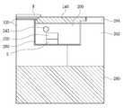
도 1에 도시된 바와 같이 본 발명의 건식 식각 장치는, 식각 공정이 수행되는 프로세스 챔버(110)와, 상기 프로세스 챔버(110) 내부에 구비되어 웨이퍼(W)가 로딩되는 페데스탈(120)과, 프로세스 챔버(110) 상,하부에 각각 설치되어 고주파(RF) 전원을 인가하는 전극 캐소드(130)와 전극 플레이트(도면부호 없음)를 포함할 수 있다.1, the dry etching apparatus of the present invention includes a
상기 프로세스 챔버(110)는, 특별히 제한되지 않으나 대략 원통형으로 제작 되고, 그 표면은 알루미늄으로 양극 산화 처리될 수 있다. 프로세스 챔버(110)의 측면 일측에는 급기구(112)가 형성되어 플라즈마 반응에 필요한 프로세스 가스를 공급하며, 바닥 일측에는 배기구(114)가 형성되어 프로세스 챔버(110) 내부를 소정 압력으로 감압할 수 있다. 상기 프로세스 챔버(110)는, 상부 챔버와 하부 챔버로 나누어 구성될 수 있으나, 여기에서는 편의상 구분없이 설명하기로 한다.The
상기 전극 캐소드(130)는, 상기 전극 플레이트의 상측에 위치하고, 전극 플레이트와 소정 거리를 두고 평행하게 설치될 수 있다. 전극 캐소드(130)는, 프로세스 가스를 프로세스 챔버(110) 내부에 균일하게 분배할 수 있도록, 샤워 헤드 구조를 취할 수 있다.The
상기 전극 플레이트는, 페데스탈(120) 내부 혹은 하부에 구비될 수 있기 때문에 별도로 도면부호를 제공하지 않았다. 즉, 페데스탈(120)은, 웨이퍼를 고정하는 기능을 수행하지만, 고주파 파워 소스를 인가하는 전극 플레이트로도 기능할 수 있다.Since the electrode plate may be provided inside or below the
여기서 상기 페데스탈(120)은, 상부에 웨이퍼(W)를 고정하는 고정척을 포함하는 개념으로 사용된다. 상기 고정척은 유전분극 현상과 정전기적 원리를 이용하여 웨이퍼(W)을 고정하는 정전척(ESC:Electro Static Chuck)에 관한 것이나, 여기에 제한되는 것은 아니고, 기계적 특성을 이용하여 웨이퍼(W)을 고정하는 진공척(Vacuum chuck) 기타 모든 고정척을 포함할 수 있다. 다만, 프로세스 챔버가 진공 상태에 있고, 진공 상호간의 압력차가 형성되지 않을 가능성이 있기 때문에, 진공척보다는 정밀 고정에 유리한 정전척(ESC)을 사용하는 것이 바람직하다. 따라 서, 정전척(ESC) 혹은 진공척은 페데스탈(Pedestal)의 상부에 별도로 구비되는 것이나, 여기서는 이들을 포함하는 것으로 사용하기로 한다.Here, the
상기 페데스탈(120)의 가장자리에는 웨이퍼(W)를 감싸는 에지 링(Edge ring: 140)이 설치된다. 에지 링(140)은, 웨이퍼(W)의 상부 표면만이 플라즈마에 노출되도록 하기 위하여, 웨이퍼(W)의 측면에 설치되는 것으로, 플라즈마를 포커싱하는 등 플라즈마를 컨펌하는 기능을 수행하기도 한다.An
한편, 로딩되는 웨이퍼(W)를 일정한 온도 상태로 유지하기 위하여 페데스탈(120) 하부에는 백 사이드용 냉각장치 혹은 가열장치(도시되지 않음)가 더 구비될 수 있다. 특히, 웨이퍼(W)의 중심과 주변에서 온도차가 존재할 수 있고, 온도차로 인해 고온에서 저온으로 플라즈마 확산이 발생할 수 있기 때문에, 온도차를 최소화하기 위하여 백 사이드용 냉각장치 혹은 가열장치는 필수적이라고 할 수 있다.Meanwhile, a cooling device or a heating device (not shown) for the backside may be further provided under the
다만, 백 사이드용 냉각장치 혹은 가열장치는, 웨이퍼(W) 중심과 주변의 온도를 조절하기 위하여, 웨이퍼(W)의 백 사이드(Back side)를 냉각 혹은 가열하기 때문에, 페데스탈 하부에 설치된다. 따라서, 웨이퍼(W)의 최외곽(Extreme edge) 부분에 대하여는 어떤식으로든 온도 조절을 수행할 수 없는 한계가 있다. 이 부분에 대하여는 좀더 자세하게 후술하겠다.The backside cooling device or heating device is installed under the pedestal to cool or heat the back side of the wafer W to adjust the temperature of the center and the periphery of the wafer W. [ Therefore, there is a limit in which the temperature adjustment can not be performed in some way with respect to the extreme edge portion of the wafer W. This part will be described in more detail below.
이와 같이, 건식 식각 공정은 폴리실리콘막 또는 옥사이드막이 적층된 웨이퍼(W)를 밀폐된 프로세스 챔버(110) 내에 장착하고, 식각용 프로세스 가스를 프로세스 챔버(110)에 주입한 다음, 고주파 혹은 마이크로 웨이브 전력 등을 인가하여 플라즈마 상태의 가스를 형성함으로써, 상기 폴리실리콘막 또는 옥사이드막을 식각할 수 있다. 이러한 건식 식각 공정은 웨이퍼(W)가 식각된 후의 세척 공정을 거칠 필요가 없을 뿐만 아니라, 폴리실리콘막 또는 옥사이드막이 이방성으로 식각되는 특성을 갖고 있다. 따라서, 건식 식각 공정은 습식 식각 공정에 비하여 고집적회로를 위한 미세 패턴 형성에 더 적합할 뿐만 아니라 식각 공정을 단순화할 수 있는 잇점이 있다.As described above, in the dry etching process, a wafer W in which a polysilicon film or an oxide film is stacked is mounted in a sealed
그런데, 건식 식각 공정(Dry etch process) 진행시 웨이퍼(W)의 온도가 일정 온도 이상으로 상승되거나 하강하면, 웨이퍼(W)의 전면에 걸쳐서 균일한 식각이 진행되지 않는 문제점이 있다.However, when the temperature of the wafer W rises or falls below a predetermined temperature during the dry etch process, uniform etching does not proceed over the entire surface of the wafer W.
여기서, 웨이퍼 전면에서 균일 식각이 진행되지 않는 이유는 여러 가지 원인이 있겠지만, 그 중에서도 웨이퍼의 표면 온도를 가장 큰 파라메터(Parameter)로 꼽을수가 있다. 웨이퍼의 표면 온도가 식각률에 영향을 미칠 수 있으며, 식각률은 표면 온도에 비례하여 높아지거나 낮아지기 때문이다. 특히 표면 온도가 과도하게 높아지거나 낮아지면 식각 제어는 전혀 이루어질 수 없게 되고, 식각 불량과 수률 저하로 귀결된다.Here, there are many reasons why the uniform etching does not proceed from the front side of the wafer. Among them, the surface temperature of the wafer is the largest parameter. The surface temperature of the wafer can affect the etch rate, and the etch rate increases or decreases in proportion to the surface temperature. In particular, if the surface temperature is excessively high or low, the etching control can not be achieved at all, resulting in poor etching and reduced yield.
식각 불량 및 수률 저하를 방지하기 위하여, 건식 식각 공정 진행중 웨이퍼(W)의 백 사이드(Back side)로 냉각 가스 혹은 고온 가스를 공급하는 냉각장치 및 가열장치를 통하여 웨이퍼(W)의 표면 온도를 제어할 수 있다. 가령, 웨이퍼(W)의 표면 온도 제어를 위하여, 웨이퍼(W)가 로딩되는 페데스탈(120)에는 웨이퍼(W)의 백 사이드(Back side)로 헬륨(He) 가스 등이 플로우되는 다수의 홀이 구비 될 수 있다.The surface temperature of the wafer W is controlled through a cooling device and a heating device for supplying a cooling gas or a high temperature gas to the back side of the wafer W during the dry etching process in order to prevent the etching failure and the decrease in the water rate can do. For example, in order to control the surface temperature of the wafer W, a plurality of holes through which helium (He) gas flows in the back side of the wafer W are formed in the
위와 같이, 웨이퍼(W)는 통상 중심과 주변에서 온도차로 인하여 균일 식각이 이루어지지 않으나, 웨이퍼(W) 중심과 주변에서의 식각 불균형은 페데스탈의 백 사이드용 냉각장치와 가열장치를 통하여 어느 정도 해결할 수 있다. 그러나, 대략 5㎜ 안밖의 웨이퍼 최외곽(Extreme edge)에서는 상기한 백 사이드용 냉각장치와 가열장치를 통해서도 해결되지 않는다.As described above, the wafer W is not uniformly etched due to the temperature difference between the center and the periphery. However, the etching imbalance at the center and the periphery of the wafer W can be solved to some extent through the pedestal backside cooling device and the heating device . However, this problem can not be solved by the above-described backside cooling device and heating device at the wafer extreme edge of about 5 mm.
일례로, 폴리실리콘막 혹은 옥사이드막이 적층된 웨이퍼(W)를 프로세스 챔버(110) 내에서 라인 앤 스페이스(L&S) 형태로 건식 식각함에 있어서, 바(Bar)의 임계 선폭(CD)을 얼마나 균일하게 형성하는지 여부가 고집적회로 형성에 관건이 된다. 그러나, 이와 같은 바(Bar)의 임계 선폭(CD)이 증가하거나 감소하는 경향이 있다. 이를 폴리실리콘막과 옥사이드막을 나누어 자세하게 살펴보면 다음과 같다.For example, when the wafer W having a polysilicon film or an oxide film stacked thereon is dry-etched in the form of L & S in the
먼저, 폴리실리콘막을 라인 앤 스페이스(L&S) 형태로 건식 식각하는 폴리 에치(Poly etch)의 경우, 라디칼 에치(Radical etch)가 진행되기 때문에, 라디칼 에천트(Radical etchant)의 밀도(Density)에 따라 식각 정도가 달라질 수 있다. 이때, 프로세스 가스로 Cl2, F 화합물 혹은 Br 화합물 등이 사용될 수 있다. 웨이퍼(W)의 최외곽 영역 밖에 있는 에지 링(140)에서는 라디칼 에천트(Radical etchant)가 소모되지 않고 그대로 머물러 있기 때문에, 웨이퍼(W) 전면에 비하여 라디칼 에천트가 풍부하다. 라디칼 에천트의 밀도가 높아지게 되면, 식각 속도(Etch rate)가 빨라지게 된다. 따라서, 에지 링(140)에서 라디칼 에천트의 밀도 가 높아지고, 인접한 웨이퍼(W)의 최외곽에서는 식각 속도가 빨라지기 때문에, 도 2 및 도 4에 도시된 바와 같이 폴리실리콘막에서 바(Bar)의 임계 선폭(CD)이 작아(Drop)지는 경향이 있다.First, in the case of a poly etch in which a polysilicon film is dry-etched in the form of a line and space (L & S), a radical etch is progressed. Therefore, depending on the density of a radical etchant, The degree of etching may vary. At this time, Cl2 , F compound, Br compound or the like may be used as the process gas. Radiant etchant is not consumed in the
다음, 옥사이드막을 라인 앤 스페이스(L&S) 형태로 건식 식각하는 옥사이드 에치(Oxide etch)의 경우, 폴리메릭 에치(Polymeric etch)가 진행되기 때문에, 폴리머(Polymer)가 발생하고, 폴리머(Polymer)의 밀도(Density)에 따라 식각 정도가 달라질 수 있다. 이때, 옥사이드는 화학적 반응 혹은 이온 충격의 도움으로 식각될 수 있다. 에지 링(140)에서 폴리머의 밀도가 높아지면 식각 속도(Etch rate)가 느려지기 때문에, 인접한 웨이퍼(W)의 최외곽에서는 식각 속도가 현저히 낮아지고, 도 2에 도시된 바와 같이 옥사이드막에서 바(Bar)의 임계 선폭(CD)은 커지는(Raise) 경향이 있다.Next, in the case of an oxide etch in which an oxide film is dry-etched in a line-and-space (L & S) form, since a polymeric etch proceeds, a polymer is generated and the density of the polymer The etching degree may vary depending on the density. At this time, the oxide can be etched with the help of chemical reaction or ion impact. As the density of the polymer increases at the
다른 예로, 반도체 소자에서 층간 배선을 연결하기 위하여 비아 콘택(Via contact)을 형성하는 콘택 에치(Contact etch)의 경우, 옥사이드 에치에서 풍부한 폴리머로 인하여 콘택이 오픈되지 않는(Not open) 경우가 종종 발생하게 된다. 이 경우에도 옥사이드막을 라인 앤 스페이스로 건식 식각하는 경우와 그 원인이 같다.As another example, in the case of a contact etch forming a via contact to connect an interlayer wiring in a semiconductor device, a contact often does not open due to the polymer rich in the oxide etch. . Even in this case, the reason for this is the same as the case of dry-etching the oxide film by line-and-space.
이와 같이, 폴리 에치 공정에서는 바(Bar)의 임계 선폭(CD)이 감소하고, 옥사이드 에치 공정에서는 바(Bar)의 임계 선폭(CD)가 증가하거나 혹은 콘택(Contact)이 오픈되지 않는 문제점이 있기 때문에, 일방적으로 온도를 내리는 자연 냉각이나 온도를 올리는 자연 가열만으로는 엑티브하게 식각을 제어할 수 없다. 또한, 웨이퍼(W)의 중심과 주변에서 온도 제어를 하는 백 사이드용 냉각장치 및 가열장치에 의해서는 더더욱 제어할 수 없다. 따라서, 식각 공정에서 사용되는 프로세스 가스에 따라 냉각 공정 혹은 가열 공정을 선택적으로 수행할 수 있도록 에지용 냉각수단 및 가열수단을 모두 구비할 수 있어야 한다.As described above, in the poly-etch process, there is a problem in that the critical dimension line CD of the bar is decreased and the critical dimension line CD of the bar is increased or the contact is not opened in the oxide etch process Therefore, it is not possible to control the etching actively by natural cooling which unilaterally reduces the temperature or natural heating which raises the temperature. Further, it is impossible to further control by the cooling apparatus and the heating apparatus for the back side which control the temperature at the center and the periphery of the wafer W. Therefore, it is necessary to be able to provide both the cooling means for the edge and the heating means so that the cooling process or the heating process can be selectively performed according to the process gas used in the etching process.
즉, 폴리실리콘막을 라인 앤 스페이스 형태로 건식 식각하는 폴리 에치(Poly etch) 공정에서는, 웨이퍼(W)의 최외곽에서의 식각 속도를 다운시키기 위하여, 인접한 에지 링(140)의 온도를 드롭시키는 냉각수단이 필요하다. 반면, 옥사이드막을 건식 식각하는 옥사이드 에치(Oxide etch) 공정에서는, 웨이퍼(W)의 최외곽에서 식각 속도를 높이기 위하여, 인접한 에지 링(W)의 온도를 상승시키는 가열수단이 필요하다. 따라서, 도 3에 도시된 바와 같이 폴리실리콘막 혹은 옥사이드막 모두에서 바(Bar)의 임계 선폭(CD)이 균일해지는 것을 알 수 있다.That is, in the poly etch process for dry-etching the polysilicon film in a line-and-space form, the temperature of the
여기서, 프로세스 챔버(110)에서 진행되는 웨이퍼 프로세스를 주로 에칭(Etching)에 관하여 설명하고 있지만, 증착(Deposition)의 경우에 대하여도 동일하게 적용될 수 있다. 가령, 웨이퍼(W)의 표면 온도가 높아지는 경우 플라즈마에 의하여 활성화된 입자(라이칼 등의 중성 입자나 이온)가 웨이퍼(W) 상에 머무는 시간이 짧아지고, 활성화된 입자의 밀도가 낮아지며, 단위 시간 당 식각 속도가 저하될 때, 단위 시간 당 식각 속도를 제어하기 위하여, 웨이퍼(W)의 표면 온도를 낮출 수 있도록 냉각수단이 요구될 수 있다. Here, although the wafer process in the
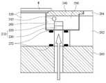
이와 같이, 도 5 내지 도 7에 도시된 바와 따르면, 에지 링(140)의 하부에는 웨이퍼(W)의 최외곽 온도를 조절하기 위하여, 열전달 기능을 수행하는 커플링 링(200)과, 커플링 링(200) 내부에 구비되고 커플링 링의 온도를 상승(Raise) 혹은 드롭(Drop)시킴으로써, 에지 링(120)을 냉각 혹은 가열시키는 에지용 냉각수단(210) 및 가열수단(240)을 더 포함한다.5 to 7, a
이 때, 본 발명의 실시예에서는 에지 링(140)의 하부에 커플링 링(200)이 링 구조물을 이루는 것으로 되어 있지만, 별도의 커플링 링(200)이 구비되지 않고, 에지용 냉각수단(210) 및 가열수단(240)이 에지 링(140)에 직접 설치될 수 있음을 배제하지 않는다.In this case, in the embodiment of the present invention, the
상기 에지 링(140)은, 폴리 에치(Poly etch) 공정에서는 쿼츠(Quartz)가 사용될 수 있으나, 옥사이드 에치(Oxide etch) 공정에서는 실리콘(Si)이 사용되며, 더 바람직하게는 세라믹 계열의 알루미나 등이 사용될 수 있다. 여기서, 옥사이드 에치 공정에서는 실리콘으로 에지 링(140)을 제작하여도 무방하지만, 폴리 에지 공정에서는 실리콘이 모두 식각될 수 있기 때문에 적합하지 않고 쿼츠를 사용해야 되나, 본 발명의 실시예에서는 옥사이드 에치와 폴리 에치를 모두 처리할 수 있어야 하고, 웨이퍼(W)의 최외곽 온도를 조절해야 하기 때문에, 에지 링(140)은 세라믹 계열의 알루미나로 구성되는 것이 바람직하다.Quartz may be used in the poly etch process, but silicon (Si) is used in the oxide etch process. More preferably, the
상기 커플링 링(200)은, 열 전달이 우수하고, 열 분포가 고른 알루미늄(Al)과 같은 금속 혹은 이와 유사한 전도성(Conductive) 물질로 구성될 수 있다. 커플링 링(200)의 내부에는 에지용 냉각수단(210) 혹은 가열수단(240)이 구비되기 때문이다.The
도 7 및 도 8에 도시된 바와 같이, 상기 페데스탈(120)과 커플링 링(200) 사이에는 온도 변화의 폭을 최소화하고, 능동적으로 온도를 제어할 수 있도록, 열 전 달을 차단하는 열 차폐막(Thermal insulator layer: 260)이 구비될 수 있다. 도면에는 도시되어 있지 않지만, 페데스탈(120)에는 웨이퍼(W)의 중심과 주변의 온도차를 해소하기 위하여, 백 사이드용 냉각장치 및 가열장치(도시되지 않음)가 더 구비될 수 있다. 특히, 본 발명의 실시예에서는 페데스탈(120)과 커플링 링(200) 양측에서 온도를 독립적으로 제어하기 위하여, 페데스탈(120)과 커플링 링(200) 사이에서 열 전달을 차단해야 할 이유가 매우 크다.As shown in FIGS. 7 and 8, between the
상기 열 차폐막(260)은, 열 차단에 우수한 알루미나와 같은 세라믹, 쿼츠 혹은 엔지니어링 플라스틱(가령, Polyimide, Teflon, Peek)등의 재료로 구성될 수 있다. 열 차폐막(260)의 두께는 0.1㎜ ∼ 10㎜ 정도로 형성되는 것이 열 차단에 적합하다.The
상기 커플링 링(200)은, 에지용 냉각수단(210) 혹은 가열수단(240) 중 어느 하나를 선택적으로 구비할 수 있다. 하지만, 폴리 에치 공정시 사용되는 프로세스 가스와 옥사이드 에치 공정시 사용되는 프로세스 가스가 각각 다를 수 있고, 이에 따라 에지 링(140)을 냉각 혹은 가열시켜야 하기 때문에, 각 공정에서 웨이퍼(W)의 최외곽 온도를 엑티브하게 조절하기 위하여 두 개의 수단을 모두 구비하는 것이 바람직하다.The
상기 냉각수단(210)은, 커플링 링(200)의 링 구조물을 따라 그 내부에 형성된 쿨런트 채널(220)과, 상기 쿨런트 채널(220)을 플로우하는 쿨런트로 구성될 수 있다. 상기 쿨런트는, 냉각수를 비롯하여 모든 냉각제가 포함될 수 있다.The cooling means 210 may include a
상기 쿨런트 채널(220)은, 링 구조물의 커플링 링(200) 내부를 쿨런트가 순 환할 수 있도록 환형 구조를 가질 수 있다. 이때, 커플링 링(200)은 그 제작이 용이한 주조(Cast)에 의하여 제작될 수 있다. 그리고, 도 9에 도시된 바와 같이 쿨런트 채널(220)을 형성하기 위하여 커플링 링(200)의 저면에 개구부(Opening: 222)를 갖는 환형의 그루브(Groove: 224)가 성형되도록 한다. 다음, 도 10에 도시된 바와 같이 그루브(224)를 따라 개구부(222)에 납땜(Brazing) 혹은 이빔 용접(B-beam welding)을 수행하게 되면, 개방된 그루브(224)가 폐쇄됨으로써 쿨런트 채널(220)이 형성된다. 따라서, 커플링 링(200)에서 쿨런트 채널(220)의 하부 스페이서(S)는 납땜(brazing)이나 이빔 용접(E-beam welding) 방식에 의하여 채워짐으로써, 납땜부 혹은 용접부가 형성될 수 있다. 납땜 혹은 용접 재료는 커플링 링(200)의 재료와 동일하거나 이와 유사하다.The
상기 쿨런트 채널(220)은, 커플링 링(200)의 링 구조물을 따라 한 번 혹은 그 이상 회전함에 따라 싱글 턴(Single-turn) 혹은 멀티 턴(Multi-turn)을 구성할 수 있다. 상기 쿨런트 채널(220)은, 쿨런트가 원활하게 플로우할 수 있도록 그 높이가 2㎜ ∼ 20㎜ 정도이고, 그 폭은 2㎜ ∼ 20㎜ 정도로 형성되는 것이 바람직하다.The
상기 쿨런트가 플로우를 시작하는 상기 환형의 쿨런트 채널(220)의 일측과 타측에는 쿨런트 채널과 수직으로 쿨런트가 공급되거나 혹은 배출되는 공급 채널과 배출 채널(230)이 각각 형성될 수 있다.A supply channel and a
상기 가열수단(240)은, 히터(Heater)로 구성될 수 있다. 상기 히터는 히터 코일(Heater coil: 242)과 히터 터미널(Heater terminal: 244)로 구성될 수 있다. 히터 코일(242)은 냉각수단 즉, 쿨런트 채널(220)과 일정한 거리를 두고 쿨런트 채널(220)의 상부에 평행하게 설치되는 것이 바람직하다. 상기 히터는, 그 파워(Power)가 50W 내지 500W 정도의 저항성 히터(Resistive heater)가 사용될 수 있다. 따라서 히터 코일(242)은, 저항 변화가 적고, 사용 수명이 비교적 긴 Ni-Cr 계열이 사용될 수 있다. 상기 히터 코일(242)은, 싱글 턴(Single-turn) 혹은 멀티 턴(Multi-turn) 모두 가능하다.The heating means 240 may be a heater. The heater may include a
상기 히터 터미널(244)은 냉각수단 즉, 쿨런트 채널(220)이 존재하지 않는 공급 채널과 배출 채널(230) 사이에 구비되는 것이 바람직하다. 따라서, 공급 채널(230)과 히터 터미널(244)은 상호 오버랩(Overlap)되지 않는 범위 내에서 커플링 링(200)의 하부에서 상부로 수직하게 연장되고, 쿨런트 채널(220)과 히터 코일(242)은 다시 환형의 커플링 링(200)에서 수평으로 순환되도록 턴(Turn)한 후, 다시 배출 채널(230)과 히터 터미널(244)은 커플링 링(200)의 상부에서 하부로 수직하게 연장될 수 있다.The
상기 히터는 제작 방식에 따라 캐스트 인 히터(Cast-in heater) 또는 타이트 피팅 히터(Tight-fitting heater)로 구분될 수 있다. 특히, 캐스트 인 히터는, 히터 코일(242)을 인서트한 상태에서 주조 하기 때문에, 커플링 링(200)에 히터 코일(242)을 원하는 형상으로 배치할 수 있어 본 발명에 매우 적합하다.The heater may be classified into a cast-in heater or a tight-fitting heater according to a manufacturing method. Particularly, since the cast-in heater casts the
상기 에지 링(140)과 커플링 링(200)은, 에폭시(Epoxy)나 실리콘(Silicone)과 같은 폴리머 본더(Polymer bonder)에 의하여 접합될 수 있다. 상기 본더의 두께는 0.05 ∼ 5㎜ 정도로 형성되는 것이 바람직하다.The
상기 페데스탈(120)과 커플링 링(200)은, 여러 가지 체결수단을 이용하여 고정될 수 있으나, 유체 상태인 쿨런트의 실링(Sealing)을 위하여 페데스탈(120)과 커플링 링(200)을 긴밀하게 결합하는 볼트(Bolt: 270)를 이용할 수 있다. 따라서, 볼트(270)가 안착될 수 있도록 쿨런트 채널(220)은 단면을 기준으로 볼 때 커플링 링(200)의 외주연을 원형으로 턴(Turn)하는 것이 아니고, 지그재그의 곡선 형태로 턴(Tunr)하는 것이 바람직하다.The
상기 쿨런트 채널(220)은 상압으로 유지되나 페데스탈(120)의 상부는 진공 상태에 있기 때문에, 압력차에 의하여 상기 쿨런트가 진공으로 유출될 수 있다. 상기 쿨런트의 실링(Sealing)을 더욱 강화하기 위하여, 쿨런트와 진공 사이를 실링(Sealing)하는 오링(O-ring: 272)이 공급 및 배출 채널(230)의 가장자리에 설치될 수 있다. 여기서, 상기 볼트(270)는 전술한 바와 같이 오링(272)이 커플링 링(200)과 페데스탈(120) 사이에 더욱 긴밀하게 밀착되도록 가압하는 기능을 수행한다.Since the
경우에 따라서, 페데스탈(120)의 하부에 절연 플레이트(Isolator plate: 280)가 더 설치되거나 절연 링(Isolator ring: 290)이 더 설치될 수 있다. 이러한 경우 쿨런트를 공급하는 공급 및 배출 채널(230)이 절연 플레이트(280)나 절연 링(282)으로 연장될 수 있다. 이러한 경우에 페데스탈(120)과 절연 플레이트(280) 혹은 절연 링(282) 사이에도 오링(272)이 더 개재될 수 있음은 물론이다.In some cases, an
상기 절연 링(282)이 더 구비되는 경우에는 절연 링의 상부에 커버 링(Cover ring: 284)이 더 구비될 수 있다. 상기 커버 링(284)은 에지 링(140)과 마찬가지 로, 프로세스 가스의 종류에 따라 실리콘(Si), 쿼츠(Quartz) 혹은 세라믹(Ceramic) 등으로 형성될 수 있다.When the insulating
한편, 상기 히터의 구동을 위하여 직류(DC) 전류가 사용되나, 플라즈마 방전을 위하여 바이어스 파워 혹은 소스 파워로 고주파(RF)를 사용하기 때문에, 히터가 고주파(RF)에 의하여 교란될 수 있다. 따라서, 바이어스 혹은 소스 RF 파워로부터 히터로 유입되는 고주파(RF)의 누출을 방지하기 위하여, 히터 터미널(244)에는 필터(Filter: 290)가 더 구비될 수 있다.On the other hand, a direct current (DC) current is used for driving the heater, but a high frequency (RF) is used as a bias power or a source power for plasma discharge, so that the heater can be disturbed by a high frequency RF. Therefore, the
이상에서 살펴본 바와 같이, 본 발명은 식각될 물질막과 사용될 프로세스 가스의 종류에 관계 없이 웨이퍼의 최외곽 영역에서 액티브하게 온도를 올리거나 내릴 수 있는 구성을 기술적 사상으로 하고 있음을 알 수 있다. 이와 같은 본 발명의 기본적인 기술적 사상의 범주 내에서, 당업계의 통상의 지식을 가진 자에게 있어서는 다른 많은 변형이 가능할 것이다.As described above, according to the present invention, it is understood that the structure is such that the temperature can be actively raised or lowered in the outermost region of the wafer regardless of the material film to be etched and the kind of process gas to be used. Many other modifications will be possible to those skilled in the art, within the scope of the basic technical idea of the present invention.
도 1은 본 발명에 의한 플라즈마 건식 식각 장치의 구성을 나타내는 개략 단면도.1 is a schematic sectional view showing a configuration of a plasma dry etching apparatus according to the present invention.
도 2는 본 발명에 의한 폴리 에치 공정 및 옥사이드 에치 공정시 웨이퍼의 최외곽 부분에서 바의 임계 선폭이 감소하거나 증가하는 경향을 나타내는 그래프.FIG. 2 is a graph showing a tendency that a critical line width of a bar in the outermost portion of a wafer decreases or increases in a poly etch process and an oxide etch process according to the present invention.
도 3은 본 발명에 의한 폴리 에치 공정 및 옥사이드 에치 공정시 웨이퍼의 최외곽 부분의 온도를 냉각시키거나 가열함으로써, 바의 임계 선폭이 균일해지는 경향을 나타내는 그래프.3 is a graph showing a tendency that the critical line width of a bar becomes uniform by cooling or heating the temperature of the outermost portion of the wafer in the poly etch process and the oxide etch process according to the present invention.
도 4는 본 발명에 의한 폴리 에치 공정 및 옥사이드 에칭 공정에서 플라즈마 반응의 차이를 보여주는 테이블.4 is a table showing differences in plasma reactions in a poly-etch process and an oxide etch process according to the present invention.
도 5는 본 발명에 의한 도 1의 Ⅰ-Ⅰ를 절단하되, 나머지 구성을 생략하고 커플링 링의 구성만을 나타내는 평단면도.Fig. 5 is a plan sectional view showing only the structure of a coupling ring, in which I-I of Fig.
도 6은 본 발명에 의한 에지용 냉각수단 및 가열수단이 구비되는 커플링 링의 구성을 나타내는 부분 절개 사시도.6 is a partially cutaway perspective view showing the structure of a coupling ring provided with cooling means for edge and heating means according to the present invention.
도 7은 본 발명에 의한 도 1의 P부분을 확대하되, 도 5의 B-B를 절단한 부분의 단면도.FIG. 7 is a cross-sectional view of a portion of FIG. 5 taken along line B-B of FIG. 1 according to the present invention.
도 8은 본 발명에 의한 도 1의 P부분을 확대하되, 도 5의 C-C를 절단한 부분의 단면도.FIG. 8 is a cross-sectional view of a portion cut along line C-C of FIG. 5 by enlarging the P portion of FIG. 1 according to the present invention. FIG.
도 9는 본 발명에 의한 커플링 링을 히터 코일이 인서트된 상태에서 주조하는 공정을 나타내는 부분 절개 사시도.9 is a partial cutaway perspective view showing a process of casting a coupling ring according to the present invention in a state in which a heater coil is inserted.
도 10은 본 발명에 의한 커플링 링의 그루브를 납땜 혹은 용접하여 쿨런트 채널을 완성하는 공정을 나나태는 부분 절개 사시도.10 is a partially cutaway perspective view showing a process of completing a coolant channel by brazing or welding a groove of a coupling ring according to the present invention.
**도면의 주요구성에 대한 부호의 설명**DESCRIPTION OF THE REFERENCE SYMBOLS
110: 프로세스 챔버112: 급기구110: process chamber 112:
114: 배기구120: 페데스탈114: exhaust port 120: pedestal
130: 케소드140: 에지 링130: Kesord 140: Edge ring
200: 커플링 링210: 에지용 냉각수단200: Coupling ring 210: Cooling means for edge
220: 쿨런트 채널222: 개구부220: Coolant channel 222: Opening
224: 그루브230: 공급 및 배출 채널224: Groove 230: Feed and discharge channel
240: 에지용 가열수단242: 히터 코일240: Edge heating means 242: Heater coil
244: 히터 터미널260: 열 차폐막244: heater terminal 260: heat shield film
270: 볼트272: 오링270: Bolt 272: O-ring
280: 절연 플레이트282: 절연 링280: insulating plate 282: insulating ring
284: 커버 링290: 필터284: Cover ring 290: Filter
Claims (10)
Translated fromKoreanPriority Applications (2)
| Application Number | Priority Date | Filing Date | Title |
|---|---|---|---|
| KR1020090057172AKR101559913B1 (en) | 2009-06-25 | 2009-06-25 | Plasma dry etching apparatus |
| US12/792,915US8555810B2 (en) | 2009-06-25 | 2010-06-03 | Plasma dry etching apparatus having coupling ring with cooling and heating units |
Applications Claiming Priority (1)
| Application Number | Priority Date | Filing Date | Title |
|---|---|---|---|
| KR1020090057172AKR101559913B1 (en) | 2009-06-25 | 2009-06-25 | Plasma dry etching apparatus |
Publications (2)
| Publication Number | Publication Date |
|---|---|
| KR20100138580A KR20100138580A (en) | 2010-12-31 |
| KR101559913B1true KR101559913B1 (en) | 2015-10-27 |
Family
ID=43379440
Family Applications (1)
| Application Number | Title | Priority Date | Filing Date |
|---|---|---|---|
| KR1020090057172AActiveKR101559913B1 (en) | 2009-06-25 | 2009-06-25 | Plasma dry etching apparatus |
Country Status (2)
| Country | Link |
|---|---|
| US (1) | US8555810B2 (en) |
| KR (1) | KR101559913B1 (en) |
Families Citing this family (27)
| Publication number | Priority date | Publication date | Assignee | Title |
|---|---|---|---|---|
| KR101559913B1 (en)* | 2009-06-25 | 2015-10-27 | 삼성전자주식회사 | Plasma dry etching apparatus |
| KR101951369B1 (en)* | 2011-09-01 | 2019-02-25 | 세메스 주식회사 | Electrostatic chuck and substrate treating apparatus including the chuck |
| US9947559B2 (en)* | 2011-10-28 | 2018-04-17 | Applied Materials, Inc. | Thermal management of edge ring in semiconductor processing |
| US9412579B2 (en)* | 2012-04-26 | 2016-08-09 | Applied Materials, Inc. | Methods and apparatus for controlling substrate uniformity |
| US20150170955A1 (en)* | 2013-12-17 | 2015-06-18 | Applied Materials, Inc. | Actively-cooled shadow ring for heat dissipation in plasma chamber |
| CN104862660B (en)* | 2014-02-24 | 2017-10-13 | 北京北方华创微电子装备有限公司 | Bogey and plasma processing device |
| US10109510B2 (en)* | 2014-12-18 | 2018-10-23 | Varian Semiconductor Equipment Associates, Inc. | Apparatus for improving temperature uniformity of a workpiece |
| US9633875B2 (en)* | 2015-03-13 | 2017-04-25 | Varian Semiconductor Equipment Associates, Inc. | Apparatus for improving temperature uniformity of a workpiece |
| KR20170127724A (en)* | 2016-05-12 | 2017-11-22 | 삼성전자주식회사 | Plasma processing apparatus |
| US9852889B1 (en) | 2016-06-22 | 2017-12-26 | Lam Research Corporation | Systems and methods for controlling directionality of ions in an edge region by using an electrode within a coupling ring |
| KR102581226B1 (en) | 2016-12-23 | 2023-09-20 | 삼성전자주식회사 | Plasma processing device |
| KR101941765B1 (en)* | 2017-01-13 | 2019-01-23 | 쿠어스택 가부시키가이샤 | Planar heater |
| US10674566B2 (en) | 2017-03-02 | 2020-06-02 | Coorstek Kk | Planar heater |
| JP7045635B2 (en)* | 2017-08-30 | 2022-04-01 | パナソニックIpマネジメント株式会社 | Plasma processing equipment and method |
| US11915850B2 (en)* | 2017-12-20 | 2024-02-27 | Applied Materials, Inc. | Two channel cosine-theta coil assembly |
| CN110323117B (en)* | 2018-03-28 | 2024-06-21 | 三星电子株式会社 | Plasma treatment equipment |
| CN111197251B (en)* | 2018-10-30 | 2022-11-04 | 青岛海尔智能技术研发有限公司 | Drying machine, control method and control device |
| US11430639B2 (en)* | 2018-12-13 | 2022-08-30 | Xia Tai Xin Semiconductor (Qing Dao) Ltd. | Plasma processing system |
| EP4336983A3 (en)* | 2019-01-04 | 2024-05-15 | Jabil, Inc. | Apparatus, system, and method of providing a circuit board carrier for an underfill system |
| US10784089B2 (en) | 2019-02-01 | 2020-09-22 | Applied Materials, Inc. | Temperature and bias control of edge ring |
| JP2021019099A (en)* | 2019-07-19 | 2021-02-15 | 東京エレクトロン株式会社 | Placement table assembly, substrate processing device, and edge ring |
| US11894255B2 (en) | 2019-07-30 | 2024-02-06 | Applied Materials, Inc. | Sheath and temperature control of process kit |
| JP2021027152A (en)* | 2019-08-05 | 2021-02-22 | キオクシア株式会社 | Plasma processing apparatus and plasma processing method |
| JP7316179B2 (en)* | 2019-10-04 | 2023-07-27 | 東京エレクトロン株式会社 | SUBSTRATE SUPPORT AND PLASMA PROCESSING APPARATUS |
| CN112259452B (en)* | 2020-10-21 | 2023-04-07 | 上海华力集成电路制造有限公司 | Control method of plasma dry etching process |
| KR20220102201A (en) | 2021-01-12 | 2022-07-20 | 삼성전자주식회사 | chuck assembly, manufacturing apparatus of semiconductor device including the same and manufacturing method of semiconductor device |
| KR102783125B1 (en)* | 2023-02-21 | 2025-03-19 | 삼성전자주식회사 | Plasma apparatus |
Citations (1)
| Publication number | Priority date | Publication date | Assignee | Title |
|---|---|---|---|---|
| US20040040933A1 (en)* | 2002-03-04 | 2004-03-04 | Seiichiro Kanno | Wafer processing apparatus and a wafer stage and a wafer processing method |
Family Cites Families (13)
| Publication number | Priority date | Publication date | Assignee | Title |
|---|---|---|---|---|
| US6024826A (en)* | 1996-05-13 | 2000-02-15 | Applied Materials, Inc. | Plasma reactor with heated source of a polymer-hardening precursor material |
| JP3257328B2 (en)* | 1995-03-16 | 2002-02-18 | 株式会社日立製作所 | Plasma processing apparatus and plasma processing method |
| US6036878A (en)* | 1996-02-02 | 2000-03-14 | Applied Materials, Inc. | Low density high frequency process for a parallel-plate electrode plasma reactor having an inductive antenna |
| EP1154466A4 (en) | 1999-01-29 | 2003-08-27 | Tokyo Electron Ltd | Method and apparatus for plasma processing |
| US6363882B1 (en)* | 1999-12-30 | 2002-04-02 | Lam Research Corporation | Lower electrode design for higher uniformity |
| JP4592916B2 (en)* | 2000-04-25 | 2010-12-08 | 東京エレクトロン株式会社 | Placement device for workpiece |
| US6492774B1 (en)* | 2000-10-04 | 2002-12-10 | Lam Research Corporation | Wafer area pressure control for plasma confinement |
| JP2002164323A (en) | 2000-11-28 | 2002-06-07 | Semiconductor Leading Edge Technologies Inc | Focusing ring and apparatus and method for treatment of substrate |
| JP4676074B2 (en)* | 2001-02-15 | 2011-04-27 | 東京エレクトロン株式会社 | Focus ring and plasma processing apparatus |
| AU2002366921A1 (en)* | 2001-12-13 | 2003-07-09 | Tokyo Electron Limited | Ring mechanism, and plasma processing device using the ring mechanism |
| US7244336B2 (en)* | 2003-12-17 | 2007-07-17 | Lam Research Corporation | Temperature controlled hot edge ring assembly for reducing plasma reactor etch rate drift |
| KR20080046822A (en) | 2006-11-23 | 2008-05-28 | 삼성전자주식회사 | Plasma processing apparatus having a control electrode inside the focus ring |
| KR101559913B1 (en)* | 2009-06-25 | 2015-10-27 | 삼성전자주식회사 | Plasma dry etching apparatus |
- 2009
- 2009-06-25KRKR1020090057172Apatent/KR101559913B1/enactiveActive
- 2010
- 2010-06-03USUS12/792,915patent/US8555810B2/enactiveActive
Patent Citations (1)
| Publication number | Priority date | Publication date | Assignee | Title |
|---|---|---|---|---|
| US20040040933A1 (en)* | 2002-03-04 | 2004-03-04 | Seiichiro Kanno | Wafer processing apparatus and a wafer stage and a wafer processing method |
Also Published As
| Publication number | Publication date |
|---|---|
| KR20100138580A (en) | 2010-12-31 |
| US20100326600A1 (en) | 2010-12-30 |
| US8555810B2 (en) | 2013-10-15 |
Similar Documents
| Publication | Publication Date | Title |
|---|---|---|
| KR101559913B1 (en) | Plasma dry etching apparatus | |
| KR102471635B1 (en) | Ultra-uniform heated substrate support assembly | |
| US6245192B1 (en) | Gas distribution apparatus for semiconductor processing | |
| US7244311B2 (en) | Heat transfer system for improved semiconductor processing uniformity | |
| KR102374523B1 (en) | Chamber apparatus for chemical etching of dielectric materials | |
| KR100726381B1 (en) | Gas distribution apparatus for semiconductor processing | |
| KR101980203B1 (en) | Support unit and substrate treating apparatus including the same | |
| CN101903996B (en) | Method and apparatus for controlling temperature of a substrate | |
| KR101476566B1 (en) | Substrate support having dynamic temperature control | |
| JP4776130B2 (en) | Plasma processing apparatus, semiconductor manufacturing apparatus, and heating / cooling block used therefor | |
| CN108335963A (en) | Plasma processing apparatus | |
| EP2088616A2 (en) | Substrate mounting table, substrate processing apparatus and substrate temperature control method | |
| JP3374033B2 (en) | Vacuum processing equipment | |
| TW200406846A (en) | Variable temperature processes for tunable electrostatic chuck | |
| US20050039854A1 (en) | Plasma etching method and plasma etching unit | |
| KR20010042268A (en) | Contamination controlling method and plasma processing chamber | |
| KR101333926B1 (en) | Substrate supporting table, substrate processing apparatus, and manufacture method for semiconductor device | |
| KR20140095031A (en) | Method of etching self-aligned vias and trenches in a multi-layer film stack | |
| JP2007507104A (en) | Method and apparatus for efficient temperature control using communication space | |
| KR102585290B1 (en) | Focus Ring and plasma device including the same | |
| KR102684970B1 (en) | Capacitively-coupled plasma substrate processing apparatus including a focus ring and a substrate processing method using the same | |
| KR100304971B1 (en) | heater block for film deposition in fabrication of semiconductor | |
| US20250218729A1 (en) | Shower head assembly and substrate processing apparatus | |
| KR20020089592A (en) | reflow equipment of semiconductor device manufacturing equipment | |
| JP2009087949A (en) | Microwave plasma device |
Legal Events
| Date | Code | Title | Description |
|---|---|---|---|
| PA0109 | Patent application | Patent event code:PA01091R01D Comment text:Patent Application Patent event date:20090625 | |
| PG1501 | Laying open of application | ||
| A201 | Request for examination | ||
| PA0201 | Request for examination | Patent event code:PA02012R01D Patent event date:20140522 Comment text:Request for Examination of Application Patent event code:PA02011R01I Patent event date:20090625 Comment text:Patent Application | |
| E902 | Notification of reason for refusal | ||
| PE0902 | Notice of grounds for rejection | Comment text:Notification of reason for refusal Patent event date:20150316 Patent event code:PE09021S01D | |
| E701 | Decision to grant or registration of patent right | ||
| PE0701 | Decision of registration | Patent event code:PE07011S01D Comment text:Decision to Grant Registration Patent event date:20150817 | |
| GRNT | Written decision to grant | ||
| PR0701 | Registration of establishment | Comment text:Registration of Establishment Patent event date:20151006 Patent event code:PR07011E01D | |
| PR1002 | Payment of registration fee | Payment date:20151007 End annual number:3 Start annual number:1 | |
| PG1601 | Publication of registration | ||
| FPAY | Annual fee payment | Payment date:20180927 Year of fee payment:4 | |
| PR1001 | Payment of annual fee | Payment date:20180927 Start annual number:4 End annual number:4 | |
| PR1001 | Payment of annual fee | Payment date:20200929 Start annual number:6 End annual number:6 | |
| PR1001 | Payment of annual fee | Payment date:20220927 Start annual number:8 End annual number:8 | |
| PR1001 | Payment of annual fee | Payment date:20240925 Start annual number:10 End annual number:10 |