KR101556314B1 - Bridge structure in conductive mesh and method for manufacturing the same - Google Patents
Bridge structure in conductive mesh and method for manufacturing the sameDownload PDFInfo
- Publication number
- KR101556314B1 KR101556314B1KR1020137030044AKR20137030044AKR101556314B1KR 101556314 B1KR101556314 B1KR 101556314B1KR 1020137030044 AKR1020137030044 AKR 1020137030044AKR 20137030044 AKR20137030044 AKR 20137030044AKR 101556314 B1KR101556314 B1KR 101556314B1
- Authority
- KR
- South Korea
- Prior art keywords
- bridge
- conductive
- directional
- directional mesh
- mesh conductive
- Prior art date
- Legal status (The legal status is an assumption and is not a legal conclusion. Google has not performed a legal analysis and makes no representation as to the accuracy of the status listed.)
- Expired - Fee Related
Links
Images


Classifications
- G—PHYSICS
- G06—COMPUTING OR CALCULATING; COUNTING
- G06F—ELECTRIC DIGITAL DATA PROCESSING
- G06F3/00—Input arrangements for transferring data to be processed into a form capable of being handled by the computer; Output arrangements for transferring data from processing unit to output unit, e.g. interface arrangements
- G06F3/01—Input arrangements or combined input and output arrangements for interaction between user and computer
- G06F3/03—Arrangements for converting the position or the displacement of a member into a coded form
- G06F3/041—Digitisers, e.g. for touch screens or touch pads, characterised by the transducing means
- G06F3/044—Digitisers, e.g. for touch screens or touch pads, characterised by the transducing means by capacitive means
- G06F3/0446—Digitisers, e.g. for touch screens or touch pads, characterised by the transducing means by capacitive means using a grid-like structure of electrodes in at least two directions, e.g. using row and column electrodes
- G—PHYSICS
- G06—COMPUTING OR CALCULATING; COUNTING
- G06F—ELECTRIC DIGITAL DATA PROCESSING
- G06F3/00—Input arrangements for transferring data to be processed into a form capable of being handled by the computer; Output arrangements for transferring data from processing unit to output unit, e.g. interface arrangements
- G06F3/01—Input arrangements or combined input and output arrangements for interaction between user and computer
- G06F3/03—Arrangements for converting the position or the displacement of a member into a coded form
- G06F3/041—Digitisers, e.g. for touch screens or touch pads, characterised by the transducing means
- G06F3/044—Digitisers, e.g. for touch screens or touch pads, characterised by the transducing means by capacitive means
- G06F3/0443—Digitisers, e.g. for touch screens or touch pads, characterised by the transducing means by capacitive means using a single layer of sensing electrodes
- G—PHYSICS
- G06—COMPUTING OR CALCULATING; COUNTING
- G06F—ELECTRIC DIGITAL DATA PROCESSING
- G06F2203/00—Indexing scheme relating to G06F3/00 - G06F3/048
- G06F2203/041—Indexing scheme relating to G06F3/041 - G06F3/045
- G06F2203/04103—Manufacturing, i.e. details related to manufacturing processes specially suited for touch sensitive devices
- G—PHYSICS
- G06—COMPUTING OR CALCULATING; COUNTING
- G06F—ELECTRIC DIGITAL DATA PROCESSING
- G06F2203/00—Indexing scheme relating to G06F3/00 - G06F3/048
- G06F2203/041—Indexing scheme relating to G06F3/041 - G06F3/045
- G06F2203/04111—Cross over in capacitive digitiser, i.e. details of structures for connecting electrodes of the sensing pattern where the connections cross each other, e.g. bridge structures comprising an insulating layer, or vias through substrate
- G—PHYSICS
- G06—COMPUTING OR CALCULATING; COUNTING
- G06F—ELECTRIC DIGITAL DATA PROCESSING
- G06F2203/00—Indexing scheme relating to G06F3/00 - G06F3/048
- G06F2203/041—Indexing scheme relating to G06F3/041 - G06F3/045
- G06F2203/04112—Electrode mesh in capacitive digitiser: electrode for touch sensing is formed of a mesh of very fine, normally metallic, interconnected lines that are almost invisible to see. This provides a quite large but transparent electrode surface, without need for ITO or similar transparent conductive material
Landscapes
- Engineering & Computer Science (AREA)
- General Engineering & Computer Science (AREA)
- Theoretical Computer Science (AREA)
- Human Computer Interaction (AREA)
- Physics & Mathematics (AREA)
- General Physics & Mathematics (AREA)
- Position Input By Displaying (AREA)
- Manufacture Of Switches (AREA)
Abstract
Translated fromKoreanDescription
Translated fromKorean본 발명은 도전성 메쉬 내 브릿지 구조물 및 이러한 브릿지 구조물을 제조하는 방법에 관련된다.
The present invention relates to a bridge structure in a conductive mesh and a method for manufacturing such a bridge structure.
용량성 터치 스크린의 도전성 패턴은 도전성 와이어(wire)로 구성된 병렬의 도전성 금속 메쉬 트레이스의 두 그룹을 포함한다. 일반적으로, 평행 금속 메쉬 트레이스의 일 그룹은 2차원 좌표에서 X축을 따라 정렬되고, 병렬 도전성 금속 메쉬 트레이스의 다른 그룹은 2차원 좌표에서 Y축 좌표를 따라 정렬된다. 금속 메쉬 트레이스의 두 그룹은 얼라인먼트내에 함께 본딩된 상이한 두 개의 기판상에 위치된다. 도전성 구조물이 터치 스크린에 적용되면, 터치 스크린은 큰 두께의 단점을 보이게 된다.
The conductive pattern of the capacitive touch screen includes two groups of parallel conducting metal mesh traces composed of conductive wires. In general, one group of parallel metal mesh traces are aligned along the X axis in two dimensional coordinates, and another group of parallel conductive metal mesh traces are aligned along Y axis coordinates in two dimensional coordinates. The two groups of metal mesh traces are placed on two different substrates bonded together in an alignment. When a conductive structure is applied to a touch screen, the touch screen exhibits a large thickness disadvantage.
터치 스크린의 두께가 커지는 문제를 해결하기 위해서, 본 발명은 터치 스크린의 두께를 감소시키기 위한 도전성 메쉬의 브릿지 구조물 및 상기 브릿지 구조물을 제조하는 방법에 관련된다.In order to solve the problem of increasing the thickness of the touch screen, the present invention relates to a bridge structure of a conductive mesh for reducing the thickness of a touch screen and a method of manufacturing the bridge structure.
본 발명의 일 측면에 따르면, 도전성 메쉬 브릿지 구조물이 제공되며, 이는 기판의 일 표면상에 형성된 제2방향 메쉬 도전성 트레이스에 전기적으로 연결되도록 구성되고, 제1방향 메쉬 도전성 트레이스는 상기 기판의 동일한 표면에 형성되며, 상기 제1방향 메쉬 도전성 트레이스 및 제2방향 메쉬 도전성 트레이스는 서로 평행하지 않으며, 제2방향 메쉬 도전성 트레이스는 제1방향 메쉬 도전성 트레이스와 교차하는 부분에서 단절되어 중단부를 형성하고, 이에 따라서 제2방향 메쉬 도전성 트레이스는 제1방향 메쉬 도전성 트레이스와 연결되지 않는다, 상기 브릿지 구조물은 하기의 구성을 포함한다:According to an aspect of the invention, a conductive mesh bridge structure is provided, which is configured to be electrically connected to a second directional mesh conductive trace formed on a surface of a substrate, wherein a first directional mesh conductive trace is formed on the same surface Wherein the first directional mesh conductive traces and the second directional mesh conductive traces are not parallel to each other and the second directional mesh conductive traces are disconnected at portions that intersect the first directional mesh conductive traces to form the stops, Thus, the second directional mesh conductive traces are not connected to the first directional mesh conductive traces. The bridge structure includes the following configuration:
제1브릿지 와이어 및 제2 브릿지 와이어, 제1브릿지 와이어 및 제2 브릿지 와이어는 상기 제2방향 메쉬 도전성 트레이스의 중단부에 형성되고, 상기 제1방향 메쉬 도전성 트레이스의 양측에 각각 배치됨;A first bridge wire and a second bridge wire, a first bridge wire, and a second bridge wire are formed in a middle portion of the second directional mesh conductive trace, and are disposed on both sides of the first directional mesh conductive trace, respectively;
상기 제1방향 메쉬 도전성 트레이스 상에 형성된 절연층;An insulating layer formed on the first directional mesh conductive trace;
상기 절연층상에 형성된 도전성 브릿지, 상기 도전성 브릿지는 제1방향 메쉬 도전성 트레이스와 절연되고, 상기 제1브릿지 와이어 및 제2브릿지 와이어와 연결됨.The conductive bridge formed on the insulating layer, the conductive bridge is insulated from the first directional mesh conductive trace, and connected to the first bridge wire and the second bridge wire.
일 실시예에서, 제1브릿지 와이어의 폭 및 제2브릿지 와이어의 폭은 1μm 내지 10μm이다.In one embodiment, the width of the first bridge wire and the width of the second bridge wire are 1 占 퐉 to 10 占 퐉.
일 실시예에서, 도전성 브릿지는 도전성 브릿지 금속 분말층이고, 도전성 브릿지 금속 분말층의 폭은 10μm 내지 20μm이다.In one embodiment, the conductive bridge is a conductive bridge metal powder layer, and the width of the conductive bridge metal powder layer is 10 [mu] m to 20 [mu] m.
일 실시예에서, 절연층의 상측 표면은 매끈한 곡면(smooth curved surface)이다.In one embodiment, the upper surface of the insulating layer is a smooth curved surface.
일 실시예에서 절연층은 포물선 형태의(parabolic-like) 절연층이다.In one embodiment, the insulating layer is a parabolic-like insulating layer.
일 실시예에서 상기 절연층은 투명 절연 도료(paint)층이다.In one embodiment, the insulating layer is a transparent insulating paint layer.
본 발명의 일 측면에 따르면, 도전성 메쉬 브릿지 구조물을 제조하는 방법이 제공되고, 브릿지 구조물은 기판의 일 표면상의 제2방향 메쉬 도전성 트레이스와 전기적으로 연결되도록 구성되고, 제1방향 메쉬 도전성 트레이스는 상기 기판의 표면에 형성되며, 상기 방법은 하기의 단계를 포함한다:According to an aspect of the invention, there is provided a method of making a conductive mesh bridge structure, wherein the bridge structure is configured to be electrically connected to a second directional mesh conductive trace on a surface of a substrate, The substrate being formed on the surface of the substrate, the method comprising the steps of:
제1브릿지 와이어 및 제2브릿지 와이어를 상기 제2방향 메쉬 도전성 트레이스의 중단부에 형성하고, 제1방향 메쉬 도전성 트레이스의 양측에 각각 배치하는 단계;Forming a first bridge wire and a second bridge wire in a middle portion of the second directional mesh conductive trace and placing the first and second bridge wires on opposite sides of the first directional mesh conductive trace, respectively;
제1방향 메쉬 도전성 트레이스상에 절연층을 형성하는 단계; 및Forming an insulating layer on the first directional mesh conductive trace; And
제1방향 메쉬 도전성 트레이스와 절연되고, 제1브릿지 와이어 및 제2브릿지 와이어에 연결되도록 절연층상에 도전성 브릿지를 형성하는 단계.Forming a conductive bridge on the insulative layer such that it is insulated from the first directional mesh conductive trace and connected to the first bridge wire and the second bridge wire.
일 실시예에서, 기판의 동일한 표면에 배치되는 제1방향 메쉬 도전성 트레이스 및 제2방향 메쉬 도전성 트레이스를 형성하는 것은 하기의 단계를 포함한다: 제1방향 메쉬 도전성 트레이스 및 제2방향 메쉬 도전성 트레이스를 기판상에 형성하고, 여기서 상기 제1방향 도전성 트레이스 및 제2방향 메쉬 도전성 트레이스는 서로 평행하지 않으며, 상기 제2방향 메쉬 도전성 트레이스는 제1방향 메쉬 도전성 트레이스와 교차하는 부분에서 단절되고, 제2방향 메쉬 도전성 트레이스는 제1방향 메쉬 도전성 트레이스와 연결되지 않는다.In one embodiment, forming the first directional mesh conductive traces and the second directional mesh conductive traces disposed on the same surface of the substrate includes the following: a first directional mesh conductive trace and a second directional mesh conductive trace, Wherein the first directional conductive traces and the second directional mesh conductive traces are not parallel to one another and the second directional mesh conductive traces are disconnected at portions that intersect the first directional mesh conductive traces, The directional mesh conductive traces are not connected to the first directional mesh conductive traces.
일 실시예에서, 상기 방법은 제1브릿지 와이어, 제2브릿지 와이어, 제1방향 메쉬 도전성 트레이스, 및 제2방향 도전성 트레이스를 기판상에 동시에 형성한다.In one embodiment, the method simultaneously forms a first bridge wire, a second bridge wire, a first directional mesh conductive trace, and a second directional conductive trace on a substrate.
일 실시예에서, 도전성 브릿지는 도전성 브릿지 금속 분말층이고, 도전성 브릿지를 절연층에 형성하여 제1방향 메쉬 도전성 트레이스와 절연시키며 이는 잉크젯 프린팅을 통해 절연층상에 금속 분말을 형성함으로써 수행된다.In one embodiment, the conductive bridge is a conductive bridge metal powder layer, and the conductive bridge is formed in the insulating layer and is insulated from the first directional mesh conductive trace, which is accomplished by forming metal powder on the insulating layer through inkjet printing.
일 실시예에서, 절연층은 투명 절연 도료층이고, 제1메쉬 도전성 트레이스상에 절연층을 형성하는 것은 투명 절연 도료를 제1방향 메쉬 도전성 트레이스에 잉크젯 프린팅함으로써 수행된다.In one embodiment, the insulating layer is a transparent insulating paint layer, and forming the insulating layer on the first mesh conductive traces is performed by inkjet printing a transparent insulating paint to the first directional mesh conductive traces.
도전성 메쉬 브릿지 구조물 및 도전성 메쉬 브릿지 구조물을 제조하는 방법에 있어서, 제1방향 메쉬 도전성 트레이스 및 제2방향 메쉬 도전성 트레이스는 동일한 기판상에 형성된다. 제1방향 메쉬 도전성 트레이스가 제2방향 메쉬 도전성 트레이스와의 교차점에서 연결되는 것을 방지하기 위해, 제2방향 메쉬 도전성 트레이스는 제1방향 메쉬 도전성 트레이스와 교차하는 부분에서 단절되어, 제2방향 메쉬 도전성 트레이스는 두 개의 분리된(discontinued) 메쉬 도전성 트레이스가된다. 제1브릿지 와이어 및 제2브릿지 와이어는 제2방향 메쉬 도전성 트레이스상에 형성되고, 제1브릿지 와이어는 도전성 브릿지를 통해 제2브릿지 와이어에 연결되고, 이에 따라서 제1방향 메쉬 도전성 트레이스의 양측에 위치된 두 개의 제2방향 메쉬 도전성 트레이스는 서로 연결된다. 또한, 도전성 브릿지는 절연층을 통해 제1방향 메쉬 도전성 트레이스와 절연된다; 제1방향 메쉬 도전성 트레이스는 제2방향 메쉬 도전성 트레이스와 연결되지 않고, 동일한 기판에 형성되어 있는 제1방향 메쉬 도전성 트레이스 및 제2방향 메쉬 도전성 트레이스의 목적이 이루어진다. 또한, 도전성 브릿지가 분리된 메쉬 도전성 트레이스를 직접 연결하기 위해 이용되고, 메쉬 도전성 트레이스 사이에 블랭크 영역에 연결되는 도전성 브릿지의 위험성이 제거된다. 또한 도전성 메쉬 브릿지 구조물이 터치 스크린에 적용되는 경우, 터치 스크린의 두께 및 비용이 줄어들고, 생산 효율이 향상된다.
In a method of making a conductive mesh bridge structure and a conductive mesh bridge structure, a first directional mesh conductive trace and a second directional mesh conductive trace are formed on the same substrate. To prevent the first directional mesh conductive traces from being connected at the intersection with the second directional mesh conductive traces, the second directional mesh conductive traces are disconnected at portions that intersect the first directional mesh conductive traces, The traces become two discontinued mesh conductive traces. The first bridge wire and the second bridge wire are formed on the second directional mesh conductive traces and the first bridge wire is connected to the second bridge wire through the conductive bridge so that the first bridge wire and the second bridge wire are positioned on both sides of the first directional mesh conductive trace The two second directional mesh conductive traces are connected to one another. Also, the conductive bridge is insulated from the first directional mesh conductive trace through the insulating layer; The first directional mesh conductive traces are not connected to the second directional mesh conductive traces, and the purpose of the first directional mesh conductive traces and second directional mesh conductive traces formed on the same substrate is accomplished. Also, the conductive bridges are used to directly connect the separated mesh conductive traces, and the risk of the conductive bridges connecting to the blank areas between the mesh conductive traces is eliminated. Also, when the conductive mesh bridge structure is applied to the touch screen, the thickness and cost of the touch screen are reduced, and the production efficiency is improved.
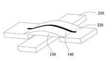
도1은 도전성 메쉬 브릿지 구조물의 개략도이다.
도2는 일 실시예에 따른 도전성 메쉬 브릿지 구조물의 부분적인 확대도이다.
도3은 도전성 메쉬 브릿지 구조물의 제조방법에 대한 순서도이다.1 is a schematic view of a conductive mesh bridge structure.
2 is a partial enlarged view of a conductive mesh bridge structure according to one embodiment.
3 is a flowchart of a method for manufacturing a conductive mesh bridge structure.
도면에 기재된 참조번호가 본 발명의 실시예의 도전성 메쉬 브릿지 구조물 밀 도전성 메쉬 브릿지 구조물을 제조하는 방법을 구체적으로 설명하기 위해 이용된다.Reference numerals in the drawings are used to specifically illustrate the method of making the conductive mesh bridge structure of the conductive mesh bridge structure of the present invention.
도1을 참조하면, 도전성 메쉬 브릿지 구조물(100)이 제공되며, 이것은 제2방향 메쉬 도전성 트레이스(220)에 전기적으로 연결되도록 구성되고, 제1방향 메쉬 도전성 트레이스(210)는 기판 표면의 동일한 표면에 형성된다. 도전성 메쉬 브릿지 구조물(100)은 제1브릿지 와이어(110), 제2브릿지 와이어(120), 절연층(130) 및 도전성 브릿지(140)를 포함한다.Referring to Figure 1, a conductive
구체적으로, 기판은 유리, 폴리에틸렌 테레프타레이트(PET; polyethylene terephthalate), 폴리카보네이트(PC; polycarbonate), 폴리메타크릴산메칠(PMMA; polymethylmethacrylate) 등과 같은 투명 물질로 만들어진다.Specifically, the substrate is made of a transparent material such as glass, polyethylene terephthalate (PET), polycarbonate (PC), polymethylmethacrylate (PMMA), or the like.
제1방향 메쉬 도전성 트레이스(210) 및 제2방향 메쉬 도전성 트레이스(220)는 서로 평행하지 않으며, 제2방향 메쉬 도전성 트레이스(220)는 제1방향 메쉬 도전성 트레이스(210)와 교차하는 부분에서 단절되어 중단부를 형성하며, 즉, 제2방향 메쉬 도전성 트레이스(220)는 두 개의 분리된 메쉬 도전성 트레이스로 나눠지고, 제2방향 메쉬 도전성 트레이스(220)는 제1방향 메쉬 도전성 트레이스(210)와 연결되지 않는다. 제1방향 메쉬 도전성 트레이스(210) 및 제2방향 메쉬 도전성 트레이스(220)는 은(silver), 구리(copper), 은과 구리의 혼합물, 또는 니켈(nickel)과 같은 재료로 만들어 질 수 있다.The first directional mesh
설명된 실시예에서, 제1방향은 수직방향이고; 제2방향은 수평방향이다. 다른 실시예에서, 제1방향은 수평방향일 수 있고, 제2방향이 수직방향일 수 있다. 또한, 서로 평행하지 않는 한 제1방향은 제2방향에 대하여 수직이 아닐 수도 있다.In the described embodiment, the first direction is the vertical direction; And the second direction is the horizontal direction. In another embodiment, the first direction may be a horizontal direction, and the second direction may be a vertical direction. Further, the first direction may not be perpendicular to the second direction unless they are parallel to each other.
제1브릿지 와이어(110) 및 제2브릿지 와이어(120)는 제2방향 메쉬 도전성 트레이스(220)의 중단부의 대향하는(opposite) 끝쪽(ends)에 형성되고, 제1브릿지 와이어(110) 및 제2브릿지 와이어(120)는 제1방향 메쉬 도전성 트레이스(210)의 양측에 각각 형성된다, 즉, 제1브릿지 와이어(110) 및 제2브릿지 와이어(120)는 제2방향 메쉬 도전성 트레이스(220)의 중단부의 경계부분에 형성된다. 메쉬 도전성 트레이스는 금속선(metal wire)을 스플라이싱(splicing)하여 형성되고, 금속선의 폭의 범위는 1μm 내지 5μm이고, 금속선 사이의 거리는 300μm 내지 500μm이다. 디자인된 브릿지 와이어의 폭이 매우 큰 경우(예컨대, 150μm 내지 500μm 이상인 경우), 명확한 브릿지 와이어가 기판상에 형성되고, 이에 따라서 터치 스크린의 광학 효율에 영향을 끼친다. 따라서 제1브릿지 와이어(110) 및 제2브릿지 와이어(120)의 폭의 범위는 일반적으로 1μm 내지 10μm이고, 이 범위는 제1브릿지 와이어(110) 및 제2브릿지 와이어(120)의 폭이 너무 커서 발생되는 터치 스크린의 광학 효율에 대한 영향을 제거할 수 있다.The
제1브릿지 와이어(110) 및 제2브릿지 와이어(120)의 길이는 제2방향 메쉬 도전성 트레이스(220)의 중단부의 단면 길이와 동일하거나 특정 상황에 따라 구성될 수 있다. 제1브릿지 와이어(110) 및 제2브릿지 와이어(120)의 길이는 금속 트레이스 사이의 거리에 배수(several or doznes of times)이고, 따라서 도전성 브릿지(140)가 분리된 메쉬 도전성 트레이스(220)에 연결되면, 도전성 브릿지(140)가 금속선이 아닌 금속선 사이의 블랭크 영역에 연결되는 위험을 피할 수 있다. 제1브릿지 와이어(110) 및 제2브릿지 와이어(120)는 은, 구리, 은과 구리의 혼합물 또는 니켈등과 같은 물질로 만들어질 수 있다.The length of the
절연층(130)은 제1방향 메쉬 도전성 트레이스(220)상에 형성된다. 절연층(130)은 일반적으로 제1브릿지 와이어(110), 제2브릿지 와이어(120) 및 제1브릿지 와이어(110) 및 제2브릿지 와이어(120)의 끝부분으로 구성된 영역상에 형성되고, 제1방향 메쉬 도전성 트레이스(210) 상에 위치된다. 특정 상황에 따라서 상이한 방법으로 이들이 구성될 수 있다는 것이 이해되어야 한다. 따라서 제1브릿지 와이어(110)가 도전성 브릿지(140)을 통해서 제2브릿지 와이어(120)와 연결된 경우, 도전성 브릿지(140)는 제1방향 메쉬 도전성 트레이스(210)와 절연된다.An
도2를 참조하면, 절연층(130)의 상측 표면은 포물선 형태의(parabolic-like) 절연층(130)과 같은 매끈한 전이 곡면(smooth transition curved surface)이 될 수 있고, 절연층(130)의 표면과 제1브릿지 와이어(110) 또는 제2브릿지 와이어(120) 사이의 높이 차이로 인해 발생되는 도전성 브릿지(140)의 단절 문제가 제거될 수 있다.2, the upper surface of the
설명된 실시예에서, 절연층(130)은 투명 절연 도료(paint)층이고, 이에 따라서 터치 스크린의 광학적 성능이 영향 받는 것을 방지한다. 투명 절연 도료층의 제1방향 메쉬 도전성 트레이스(210) 상에 고정시키기 위해 잉크젯 프린팅(ink-jet printing)으로 형성될 수 있으며 이것은 간단하고 편리하다. 다른 실시예에서, 절연층(130)은 투명하지 않을 수 있고, 절연층(130)의 폭은 터치 스크린의 광학 성능이 영향 받지 않을 만큼 제한되어야 한다.In the illustrated embodiment, the
도전성 브릿지(140)는 절연층(130)상에 형성되어 제1방향 메쉬 도전성 트레이스(210)와 절연되고, 제1브릿지 와이어는 도전성 브릿지(140)를 통해 제2브릿지 와이어(120)와 연결된다.The
도전성 브릿지(140)의 폭은 10μm 내지 20μm의 범위를 갖도록 구성될 수 있다. 따라서 도전성 브릿지(140)가 제1브릿지 와이어(110) 및 제2브릿지 와이어(120)에 연결하는 것은 편리하며, 매우 큰 도전성 브릿지(140)의 폭으로 인해 발생되는 터치 스크린의 광학 성능상의 영향은 제거될 수 있다.The width of the
도전성 브릿지(140)는 와이어 또는 금속 분말층일 수 있다. 설명된 실시예에서, 도전성 브릿지(140)는 도전성 브릿지 금속 분말층이고, 이것은 절연층(130)을 고정시키기 위해 잉크젯 프린팅으로 형성될 수 있다, 이는 간단하고 편리하다. 그 후, 도전성 브릿지(140)는 제1브릿지 와이어(110) 및 제2브릿지 와이어(120)에 레이저 얼라인(laser-laigned)을 통해 연결되어 연결 속도 및 정확성을 향상시킬 수 있다. 도전성 브릿지(140)는 은, 구리, 은과 구리의 혼합물 또는 니켈등으로 만들어 질 수 있다.The
도전성 메쉬 브릿지 구조물(100)에서, 제1방향 메쉬 도전성 트레이스(210) 및 제2방향 메쉬 도전성 트레이스(220)는 동일한 기판상에 형성되고, 제2방향 메쉬 도전성 트레이스(220)는 제1방향 메쉬 도전성 트레이스(210)와 교차하는 부분에서 단절되어 제1방향 메쉬 도전성 트레이스(210)가 교차점에서 제2방향 메쉬 도전성 트레이스(220)와 연결되는 것을 방지하고, 제2방향 메쉬 도전성 트레이스(220)는 두 개의 분리된 메쉬 도전성 트레이스로 나눠진다. 제1브릿지 와이어(110) 및 제2브릿지 와이어(120)는 제2방향 메쉬 도전성 트레이스(220)상에 형성되기 때문에, 제1브릿지 와이어(110)는 도전성 브릿지(140)를 통해 제2브릿지 와이어(120)와 연결되어, 제1방향 메쉬 도전성 트레이스(210)의 양측에 위치된 두 개의 제2방향 메쉬 도전성 트레이스(220)가 연결된다. 또한, 도전성 브릿지(140)는 절연층(130)을 통해 제1방향 메쉬 도전성 트레이스(210)와 절연되고; 제1방향 메쉬 도전성 트레이스(210)는 제2방향 메쉬 도전성 트레이스(220)와 연결되지 않으며, 동일한 기판상에 형성되어 있는 제1방향 메쉬 도전성 트레이스(210) 및 제2방향 메쉬 도전성 트레이스(220)의 목적이 이뤄진다. 또한, 도전성 브릿지(140)가 분리된 제2방향 메쉬 도전성 트레이스(220)에 연결되는데 직접 이용되는 경우, 도전성 브릿지(140)가 메쉬 도전성 트레이스 사이의 블랭크 영역에 연결되는 위험성이 제거된다. 또한, 도전성 메쉬 브릿지 구조물(100)이 터치 스크린에 적용되는 경우, 터치 스크린의 두께 및 비용이 줄어들고, 생산 효율이 향상된다.In the conductive
도3을 참조하면, 동일한 기판상에 형성된 제1방향 메쉬 도전성 트레이스(210) 및 제2방향 메쉬 도전성 트레이스(220)을 연결하기 위한 도전성 메쉬 브릿지 구조물(100)을 제조하는 방법이 제공되며, 이 방법은 아래 단계를 포함한다:3, there is provided a method of fabricating a conductive
단계(S110): 제1브릿지 와이어(110) 및 제2브릿지 와이어(120)가 제2방향 메쉬 도전성 트레이스(220)의 중단부에 형성(laid)된다.Step S110: The
제1브릿지 와이어(110) 및 제2브릿지 와이어(120)는 제2방향 메쉬 도전성 트레이스(220)의 중단부의 경계부분에 형성되고, 제1방향 메쉬 도전성 트레이스(210)의 양측에 각각 형성된다. 제1브릿지 와이어(110) 및 제2브릿지 와이어(120)는 은, 구리, 은과 구리의 혼합물, 또는 니켈등으로 만들어 질 수 있다.The
구체적으로, 제1브릿지 와이어(110) 및 제2브릿지 와이어(120)의 길이는 제2방향 메쉬 도전성 트레이스(220)의 중단부의 단면 길이(sectional length)와 동일하도록 구성될 수 있다. 이는 특별한 상황에 있어서 이렇게 구성될 수 있음이 이해되어야 한다. 제1브릿지 와이어(110) 및 제2브릿지 와이어(120)의 길이는 금속선(metal line)사이의 길이의 배수(several or dozens of times)일 수 있다는 것이 이해되어야 하며, 따라서 도전성 브릿지(140)가 단절된 메쉬 도전성 트레이스(220)에 연결된 경우, 금속선이 아닌 금속선 사이의 블랭크 영역에 연결되는 도전성 브릿지(140)의 위험이 제거될 수 있다.Specifically, the length of the
단계(S120): 절연층(130)은 제1방향 메쉬 도전성 트레이스(210) 상에 형성(배치)된다.Step (S120): The insulating
절연층(130)을 형성하는 원리는: 도전성 브릿지(140)가 형성될 때, 제1브릿지 와이어(110) 및 제2브릿지 와이어(120)에 연결되어 절연되는 제1방향 메쉬 도전성 트레이스(210) 및 도전성 브릿지(140)에 편리하다. 따라서 절연층(130)은 제1브릿지 와이어(110), 제2브리지 와이어(120) 및 제1브릿지 와이어(110) 및 제2브릿지 와이어(120)의 끝부분으로 구성된 영역에 형성되고, 제1방향 메쉬 도전성 트레이스(210)상에 위치된다. 절연층(130)은 포물선 형태의(parabolic-like) 절연층(130)과 같은 매끈한 전이 곡면(smooth transition curved surface)으로 구성될 수 있고, 절연층(130)의 표면과 제1브릿지 와이어(110) 또는 제2브릿지 와이어(120) 사이의 높이차이로 인해 발생되는 도전성 브릿지(140)의 단절 문제가 제거될 수 있다.The principle of forming the insulating
설명된 실시예에서, 절연층(130)은 투명 절연 도료(paint)층이고, 이에 따라서 터치 스크린의 광학적 성능이 영향 받는 것을 방지한다. 투명 절연 도료층의 제1방향 메쉬 도전성 트레이스(210) 상에 고정시키기 위해 잉크젯 프린팅(ink-jet printing)으로 형성될 수 있으며 이것은 간단하고 편리하다. 다른 실시예에서, 절연층(130)은 투명하지 않을 수 있고, 절연층(130)의 폭은 터치 스크린의 광학 성능이 영향 받지 않을 만큼 제한되어야 한다.In the illustrated embodiment, the insulating
단계(S130): 도전성 브릿지가 절연층(130)상에 형성된다.Step S130: A conductive bridge is formed on the insulating
도전성 브릿지(140)가 제1방향 메쉬 도전성 트레이스(210)와 절연되고; 제1브릿지 와이어(110)가 제2브릿지 와이어(120)와 도전성 브릿지(140)을 통해 연결된다. 도전성 브릿지(140)은 은, 구리, 은과 구리의 혼합물 또는 니켈등으로 만들어질 수 있다. 도전성 브릿지(140)는 와이어(wire) 또는 금속 분말층이될 수 있다. 설명된 실시예에서, 도전성 브릿지(140)는 도전성 브릿지 금속 분말층이고, 이것은 절연층(130)상에 고정하기 위해 잉크젯 프린팅으로 형성될 수 있으며 이는 간단하고 편리하다. 이 경우, 도전성 브릿지(140)는 제1브릿지 와이어(110) 및 제2브릿지 와이어(120)와 레이저-얼라인(laser-aligned)을 통해 연결되어 연결 속도 및 정확성을 향상시킨다.The
상기 단계들에서, 제1브릿지 와이어(110) 및 제2브릿지 와이어(120)의 폭은 1μm 내지 10μm의 범위로 구성될 수 있고; 도전성 브릿지(140)의 폭은 10μm 내지 20μm의 범위로 구성될 수 있다. 따라서 도전성 브릿지(140)가 제1브릿지 와이어(110), 제2브릿지 와이어(120)에 연결되는 것은 편리하고, 제1브릿지 와이어(110), 제2브릿지 와이어(120) 및 도전성 브릿지의 폭이 매우 커서 발생되는 터치 스크린의 광학 성능의 영향은 제거될 수 있다.In the above steps, the widths of the
동일한 기판상의 제1방향 메쉬 도전성 트레이스(210) 및 제2방향 메쉬 도전성 트레이스(220)를 제조하는 단계는: 제1방향 도전성 트레이스(210) 및 제2방향 도전성 트레이스(220)가 기판상에 형성된다.The step of fabricating the first directional mesh conductive traces 210 and the second directional mesh conductive traces 220 on the same substrate includes: forming first directional
기판은 유리, 폴리에틸렌 테레프타레이트(PET; polyethylene terephthalate), 폴리카보네이트(PC; polycarbonate), 폴리메타크릴산메칠(PMMA; polymethylmethacrylate) 등과 같은 투명 물질로 만들어진다.The substrate is made of a transparent material such as glass, polyethylene terephthalate (PET), polycarbonate (PC), polymethylmethacrylate (PMMA), or the like.
제1방향 메쉬 도전성 트레이스(210) 및 제2방향 메쉬 도전성 트레이스(220)는 동일한 기판상에 형성되고, 제1방향 메쉬 도전성 트레이스(210) 및 제2방향 메쉬 도전성 트레이스(220)는 서로 평행하지 않으며, 제2방향 메쉬 도전성 트레이스(220)는 제1방향 메쉬 도전성 트레이스(210)와 교차하는 부분에서 단절되어 제2방향 메쉬 도전성 트레이스(220)는 제1방향 메쉬 도전성 트레이스(210)와 연결되지 않는다.The first directional mesh conductive traces 210 and the second directional mesh conductive traces 220 are formed on the same substrate and the first directional mesh conductive traces 210 and the second directional mesh conductive traces 220 are parallel to each other And the second directional mesh conductive traces 220 are disconnected at portions that intersect the first directional mesh conductive traces 210 so that the second directional mesh conductive traces 220 are connected to the first directional mesh conductive traces 210 Do not.
설명된 실시예에서, 제1방향은 수직방향이고; 제2방향은 수평방향이다. 다른 실시예에서, 제1방향은 수평방향일 수 있고, 제2방향이 수직방향일 수 있다. 또한, 서로 평행하지 않는 한 제1방향은 제2방향에 대하여 수직이 아닐 수도 있다. 제1방향 메쉬 도전성 트레이스(210) 및 제2방향 메쉬 도전성 트레이스(220)는 은, 구리, 은과 구리의 혼합물 또는 니켈로 만들어 질 수 있다.In the described embodiment, the first direction is the vertical direction; And the second direction is the horizontal direction. In another embodiment, the first direction may be a horizontal direction, and the second direction may be a vertical direction. Further, the first direction may not be perpendicular to the second direction unless they are parallel to each other. The first directional mesh conductive traces 210 and the second directional mesh conductive traces 220 may be made of silver, copper, a mixture of silver and copper, or nickel.
특정 동작에 있어서, 제1브릿지 와이어(110), 제2브릿지 와이어(120), 제1방향 메쉬 도전성 트레이스(210) 및 제2방향 메쉬 도전성 트레이스(220)는 동시에 형성될 수 있으며, 즉 제1브릿지 와이어(110), 제2브릿지 와이어(120), 제1방향 메쉬 도전성 트레이스(210), 제2방향 메쉬 도전성 트레이스(220)는 기판상에 동시에 형성될 수 있다. 따라서 기계적인 처리공정 및 비용이 줄어든다.The
제1방향 메쉬 도전성 트레이스(210) 및 제2방향 메쉬 도전성 트레이스(220)는 동일한 기판상에 형성되고, 제1방향 메쉬 도전성 트레이스(210)가 제2방향 메쉬 도전성 트레이스(220)와 교차점에서 연결되는 것을 방지하기 위해, 제2방향 메쉬 도전성 트레이스(220)는 제1방향 메쉬 도전성 트레이스(210)와 교차하는 부분에서 단절되고, 제2방향 메쉬 도전성 트레이스(220)는 두 개의 분리된 메쉬 도전성 트레이스로 나눠진다. 도전성 메쉬 브릿지 구조물(100)을 제조하는 방법에 있어서, 제1브릿지 와이어(110) 및 제2브릿지 와이어(120)가 제2방향 메쉬 도전성 트레이스(220)상에 형성되고, 제1브릿지 와이어(110)는 도전성 브릿지(140)를 통해 제2브릿지 와이어(120)에 연결되어, 제1방향 메쉬 도전성 트레이스(210)의 양측에 위치된 두 개의 제2방향 메쉬 도전성 트레이스(220)가 연결된다. 또한, 도전성 브릿지(140)는 절연층(130)을 통해서 제1방향 메쉬 도전성 트레이스(210)와 절연되고, 제1방향 메쉬 도전성 트레이스(210)는 제2방향 메쉬 도전성 트레이스(220)와 연결되지 않아서 동일한 기판의 표면상에 제1방향 메쉬 도전성 트레이스(210) 및 제2방향 메쉬 도전성 트레이스(220)를 형성하는 목적이 이루어진다. 또한 도전성 브릿지(140)가 제2방향 메쉬 도전성 트레이스(220)에 연결되는데 직접 이용되는 경우, 도전성 브릿지(140)가 메쉬 도전성 트레이스 사이의 블랭크 영역에 연결되는 위험성이 제거된다. 또한 도전성 메쉬 브릿지 구조물(100)이 터치 스크린에 적용되면, 터치 스크린의 두께 및 비용이 감소되어 생산 효율이 향상된다.The first directional mesh conductive traces 210 and the second directional mesh conductive traces 220 are formed on the same substrate and the first directional mesh conductive traces 210 are connected to the second directional mesh conductive traces 220 at their intersections The second directional mesh conductive traces 220 are cut at portions that intersect the first directional mesh conductive traces 210 and the second directional mesh conductive traces 220 are separated from the two separate mesh conductive traces 210. [ . A method of making a conductive mesh bridge structure (100), wherein a first bridge wire (110) and a second bridge wire (120) are formed on a second directional mesh conductive trace (220) Are connected to the
상기 예시들의 설명은 구체적이고 자세하지만, 이러한 설명들이 본 발명을 제한하는데 이용될 수는 없다는 것이 이해되어야 한다. 따라서 특허 발명의 보호범위는 첨부된 청구범위에 의해 정해져야 한다.It should be understood that the description of the above examples is specific and specific, but such descriptions are not used to limit the present invention. Accordingly, the scope of protection of the patented invention should be determined by the appended claims.
Claims (11)
Translated fromKorean상기 제2방향 메쉬 도전성 트레이스의 상기 중단부에 형성되고, 상기 제1방향 메쉬 도전성 트레이스의 양측에 각각 배치된 제1 브릿지 와이어 및 제2 브릿지 와이어;
상기 제1방향 메쉬 도전성 트레이스상에 형성된 절연층; 및
상기 절연층 상에 형성되고, 상기 제1방향 도전성 트레이스에 대하여 절연되고, 상기 제1브릿지 와이어 및 상기 제2브릿지 와이어에 연결된 도전성 브릿지를 포함하되,
상기 제1브릿지 와이어 및 제2 브릿지 와이어의 길이는 상기 제2방향 메쉬 도전성 트레이스의 금속 트레이스 사이의 거리의 배수인 것을 특징으로 하는 도전성 메쉬 브릿지 구조물.
A conductive mesh bridge structure electrically connected to a second directional meshed conductive trace formed on the surface of the substrate comprises: a first directional mesh conductive trace formed on the surface of the substrate, the first directional mesh conductive trace and Wherein the second directional conductive traces are not parallel to each other and the second directional mesh conductive traces are broken at a portion that intersects the first directional mesh conductive traces to form an interrupting portion, The two-way mesh conductive traces are not connected to the first directional mesh conductive traces;
A first bridge wire and a second bridge wire formed in the middle portion of the second directional mesh conductive trace and disposed on both sides of the first directional mesh conductive trace, respectively;
An insulating layer formed on the first directional mesh conductive trace; And
A conductive bridge formed on the insulating layer and insulated with respect to the first directional conductive traces and connected to the first bridge wire and the second bridge wire,
Wherein the length of the first bridge wire and the second bridge wire is a multiple of a distance between the metal traces of the second directional mesh conductive traces.
제1브릿지 와이어 및 제2브릿지 와이어의 폭은 1μm 내지 10μm인 것을 특징으로 하는 도전성 메쉬 브릿지 구조물.
The method according to claim 1,
Wherein the widths of the first bridge wire and the second bridge wire are 1 占 퐉 to 10 占 퐉.
상기 도전성 브릿지는 도전성 브릿지 금속 분말층이고, 상기 도전성 브릿지 금속 분말층의 폭은 10μm 내지 20μm인 것을 특징으로 하는 도전성 메쉬 브릿지 구조물.
The method according to claim 1,
Wherein the conductive bridge is a conductive bridge metal powder layer, and the width of the conductive bridge metal powder layer is 10 to 20 占 퐉.
상기 절연층의 상측 표면은 매끈한 곡면(smooth curved surface)인 것을 특징으로 하는 도전성 메쉬 브릿지 구조물.
The method according to claim 1,
Wherein the upper surface of the insulating layer is a smooth curved surface.
상기 절연층은 포물선 형태의(parabolic-like) 절연층인 것을 특징으로 하는 도전성 메쉬 브릿지 구조물.
5. The method of claim 4,
Wherein the insulating layer is a parabolic-like insulating layer. ≪ RTI ID = 0.0 > 11. < / RTI >
상기 절연층은 투명 절연 도료(paint)층인 것을 특징으로 하는 도전성 메쉬 브릿지 구조물.
The method according to claim 1,
Wherein the insulating layer is a transparent insulating paint layer.
상기 제2방향 메쉬 도전성 트레이스의 중단부에 형성되고, 상기 제1방향 메쉬 도전성 트레이스의 양측에 각각 배치된 제1브릿지 와이어 및 제2 브릿지 와이어를 형성하는 단계;
상기 제1방향 메쉬 도전성 트레이스 상에 절연층을 형성하는 단계; 및
상기 제1방향 메쉬 도전성 트레이스와 절연되고, 상기 제1브릿지 와이어 및 상기 제2브릿지 와이어와 연결되도록 상기 절연층상에 도전성 브릿지를 형성하는 단계를 포함하되,
상기 제1브릿지 와이어 및 제2 브릿지 와이어의 길이는 상기 제2방향 메쉬 도전성 트레이스의 금속 트레이스 사이의 거리의 배수인 것을 특징으로 하는 도전성 메쉬 브릿지 구조물을 제조하는 방법.
A method for fabricating a conductive mesh bridge structure electrically connected to a second directional mesh conductive trace formed on a surface of a substrate, the method comprising: forming a first directional mesh conductive trace on a surface of the substrate;
Forming a first bridge wire and a second bridge wire, which are formed at a middle portion of the second directional mesh conductive trace and are disposed on both sides of the first directional mesh conductive trace, respectively;
Forming an insulating layer on the first directional mesh conductive trace; And
And forming a conductive bridge on the insulating layer to be insulated from the first directional mesh conductive trace and connected to the first bridge wire and the second bridge wire,
Wherein the length of the first bridge wire and the second bridge wire is a multiple of a distance between the metal traces of the second directional mesh conductive traces. ≪ RTI ID = 0.0 > 11. < / RTI >
상기 기판의 동일한 표면에 배치된 상기 제1방향 메쉬 도전성 트레이스 및 상기 제2방향 메쉬 도전성 트레이스를 형성하는 것은:
상기 제1방향 메쉬 도전성 트레이스 및 상기 제2방향 메쉬 도전성 트레이스를 상기 기판상에 형성하는 것을 포함하고,
상기 제1방향 메쉬 도전성 트레이스 및 상기 제2방향 메쉬 도전성 트레이스는 서로 평행하지 않으며, 상기 제2방향 메쉬 도전성 트레이스는 상기 제1방향 메쉬 도전성 트레이스와 교차하는 부분에서 단절되고, 상기 제2방향 메쉬 도전성 트레이스는 상기 제1방향 메쉬 도전성 트레이스와 연결되지 않는 것을 특징으로 하는 도전성 메쉬 브릿지 구조물을 제조하는 방법.
8. The method of claim 7,
Forming the first directional mesh conductive traces and the second directional mesh conductive traces disposed on the same surface of the substrate:
Forming the first directional mesh conductive trace and the second directional mesh conductive trace on the substrate,
Wherein the first directional mesh conductive traces and the second directional mesh conductive traces are not parallel to one another and the second directional mesh conductive traces are disconnected at portions that intersect the first directional mesh conductive traces, Wherein the traces are not connected to the first directional mesh conductive traces. ≪ Desc / Clms Page number 20 >
상기 제1브릿지 와이어, 상기 제2브릿지 와이어, 상기 제1방향 메쉬 도전성 트레이스, 및 제2방향 메쉬 도전성 트레이스를 상기 기판상에 형성하는 단계는 동시에 형성하는 것을 특징으로 하는 도전성 메쉬 브릿지 구조물을 제조하는 방법.
9. The method of claim 8,
Wherein the step of forming the first bridge wire, the second bridge wire, the first directional mesh conductive trace, and the second directional mesh conductive trace on the substrate is simultaneously performed. Way.
상기 도전성 브릿지는 도전성 브릿지 금속 분말층이고, 상기 제1방향 메쉬 도전성 트레이스와 절연되도록 상기 도전성 브릿지를 상기 절연층상에 형성하는 것은 상기 절연층 상에 금속 분말을 잉크젯-프린팅함으로써 수행되는 것을 특징으로 하는 도전성 메쉬 브릿지 구조물을 제조하는 방법.
8. The method of claim 7,
Wherein the conductive bridge is a conductive bridge metal powder layer and forming the conductive bridge on the insulating layer so as to be insulated from the first directional mesh conductive trace is performed by inkjet printing a metal powder on the insulating layer. A method for fabricating a conductive mesh bridge structure.
상기 절연층은 투명 절연 도료층이고, 상기 제1방향 메쉬 도전성 트레이스상에 상에 절연층을 형성하는 것은 상기 제1방향 메쉬 도전성 트레이스상에 투명 절연 도료를 잉크젯-프린팅함으로써 수행되는 것을 특징으로 하는 도전성 메쉬 브릿지 구조물을 제조하는 방법.8. The method of claim 7,
Wherein the insulating layer is a transparent insulating paint layer and forming the insulating layer on the first directional mesh conductive traces is performed by inkjet printing a transparent insulating paint on the first directional mesh conductive traces. A method for fabricating a conductive mesh bridge structure.
Applications Claiming Priority (3)
| Application Number | Priority Date | Filing Date | Title |
|---|---|---|---|
| CN201310071856.3 | 2013-03-06 | ||
| CN201310071856.3ACN103176678B (en) | 2013-03-06 | 2013-03-06 | Conductive grid bridging structure and manufacturing method thereof |
| PCT/CN2013/078944WO2014134893A1 (en) | 2013-03-06 | 2013-07-06 | Conductive grid bridging structure and manufacturing method thereof |
Publications (2)
| Publication Number | Publication Date |
|---|---|
| KR20140131855A KR20140131855A (en) | 2014-11-14 |
| KR101556314B1true KR101556314B1 (en) | 2015-09-30 |
Family
ID=48636604
Family Applications (1)
| Application Number | Title | Priority Date | Filing Date |
|---|---|---|---|
| KR1020137030044AExpired - Fee RelatedKR101556314B1 (en) | 2013-03-06 | 2013-07-06 | Bridge structure in conductive mesh and method for manufacturing the same |
Country Status (5)
| Country | Link |
|---|---|
| JP (1) | JP5934834B2 (en) |
| KR (1) | KR101556314B1 (en) |
| CN (1) | CN103176678B (en) |
| TW (1) | TWI497392B (en) |
| WO (1) | WO2014134893A1 (en) |
Families Citing this family (7)
| Publication number | Priority date | Publication date | Assignee | Title |
|---|---|---|---|---|
| CN103176678B (en)* | 2013-03-06 | 2014-05-07 | 南昌欧菲光科技有限公司 | Conductive grid bridging structure and manufacturing method thereof |
| JP6180174B2 (en)* | 2013-05-08 | 2017-08-16 | グンゼ株式会社 | Touch panel, display device and electronic device |
| CN105549798A (en)* | 2014-10-30 | 2016-05-04 | 中强光电股份有限公司 | Touch projection screen and projection system using same |
| CN105335034B (en)* | 2015-12-08 | 2019-03-12 | 赵宗轩 | Two-sided capacitance plate functional sheet of metal grill monofilm and preparation method thereof |
| CN105677092B (en) | 2016-01-04 | 2019-05-10 | 京东方科技集团股份有限公司 | Panel, method of making the same, and display device |
| CN106843625B (en)* | 2017-01-18 | 2020-01-14 | 业成科技(成都)有限公司 | Reduced visibility metal grid structure and method of making the same |
| CN108388363B (en)* | 2018-01-18 | 2020-12-15 | 深圳市志凌伟业技术股份有限公司 | Electrode structure for touch control |
Citations (3)
| Publication number | Priority date | Publication date | Assignee | Title |
|---|---|---|---|---|
| JP2006344163A (en)* | 2005-06-10 | 2006-12-21 | Nissha Printing Co Ltd | Electrostatic capacitance touch panel |
| JP2009009574A (en)* | 2007-06-28 | 2009-01-15 | Sense Pad Tech Co Ltd | Capacitive-type touch panel |
| US20120319990A1 (en)* | 2011-06-14 | 2012-12-20 | Chien-Ting Chan | Touch display device |
Family Cites Families (8)
| Publication number | Priority date | Publication date | Assignee | Title |
|---|---|---|---|---|
| KR101474897B1 (en)* | 2009-12-28 | 2014-12-19 | 쿄세라 코포레이션 | Input device and display device provided with same |
| JP5685411B2 (en)* | 2010-10-01 | 2015-03-18 | 京セラディスプレイ株式会社 | Touch panel |
| JP5520776B2 (en)* | 2010-10-20 | 2014-06-11 | 信越ポリマー株式会社 | Sensor sheet and manufacturing method thereof |
| CN102681734A (en)* | 2011-03-07 | 2012-09-19 | 昆山维信诺显示技术有限公司 | Capacitor touch screen and manufacturing method thereof |
| CN202150102U (en)* | 2011-07-27 | 2012-02-22 | 昆山维信诺显示技术有限公司 | Capacitive touch sensitive device |
| CN202748763U (en)* | 2012-07-13 | 2013-02-20 | 宸鸿光电科技股份有限公司 | Conductive pattern structure of capacitive touch panel |
| CN202735635U (en)* | 2012-08-10 | 2013-02-13 | 上海天马微电子有限公司 | Color film substrate and embedded touch liquid crystal display panel with same |
| CN103176678B (en)* | 2013-03-06 | 2014-05-07 | 南昌欧菲光科技有限公司 | Conductive grid bridging structure and manufacturing method thereof |
- 2013
- 2013-03-06CNCN201310071856.3Apatent/CN103176678B/enactiveActive
- 2013-07-06WOPCT/CN2013/078944patent/WO2014134893A1/enactiveApplication Filing
- 2013-07-06KRKR1020137030044Apatent/KR101556314B1/ennot_activeExpired - Fee Related
- 2013-07-06JPJP2015503747Apatent/JP5934834B2/ennot_activeExpired - Fee Related
- 2013-09-23TWTW102134022Apatent/TWI497392B/ennot_activeIP Right Cessation
Patent Citations (3)
| Publication number | Priority date | Publication date | Assignee | Title |
|---|---|---|---|---|
| JP2006344163A (en)* | 2005-06-10 | 2006-12-21 | Nissha Printing Co Ltd | Electrostatic capacitance touch panel |
| JP2009009574A (en)* | 2007-06-28 | 2009-01-15 | Sense Pad Tech Co Ltd | Capacitive-type touch panel |
| US20120319990A1 (en)* | 2011-06-14 | 2012-12-20 | Chien-Ting Chan | Touch display device |
Also Published As
| Publication number | Publication date |
|---|---|
| KR20140131855A (en) | 2014-11-14 |
| TW201435697A (en) | 2014-09-16 |
| JP5934834B2 (en) | 2016-06-15 |
| WO2014134893A1 (en) | 2014-09-12 |
| CN103176678A (en) | 2013-06-26 |
| CN103176678B (en) | 2014-05-07 |
| TWI497392B (en) | 2015-08-21 |
| JP2015512112A (en) | 2015-04-23 |
Similar Documents
| Publication | Publication Date | Title |
|---|---|---|
| KR101556314B1 (en) | Bridge structure in conductive mesh and method for manufacturing the same | |
| TWI467449B (en) | Capacitive touch panel and method for producing the same | |
| JP5838131B2 (en) | Method for manufacturing a touch-on-lens device | |
| KR102237790B1 (en) | Touch panel | |
| KR20140121811A (en) | Touch module and manufacture method thereof | |
| TWI489362B (en) | Touch sensor structures and methods of forming the same | |
| CN104460092A (en) | Display panel, display device and manufacturing method of display panel | |
| KR20130051408A (en) | Touch electrode structure and a method for manufacturing the same | |
| CN104699308B (en) | A kind of preparation method of contact panel, contact panel and touch control display apparatus | |
| US20170329455A1 (en) | Touch panel and touch display screen | |
| US9891768B2 (en) | Touch panel, its manufacturing method and touch display device | |
| CN104111747A (en) | Touch panel | |
| JP5866059B2 (en) | Touch screen conductive layer | |
| CN106896968B (en) | Touch panel capable of avoiding exposure of etched circuit | |
| TWI441067B (en) | Transparent touch pad and a method for manufacturing the same | |
| US9952697B2 (en) | Touch module and manufacturing method thereof | |
| US9287644B2 (en) | Bridge structure in conductive mesh and method for manufacturing the same | |
| KR20140014083A (en) | Touch sensor, touch screen and display device | |
| KR101400700B1 (en) | Interface panel for display and method of fabricating thereof | |
| TW201525795A (en) | Method for making touch panel | |
| CN103176677B (en) | Touch screen conductive structure and manufacturing method | |
| CN102830831B (en) | A kind of method for making of panel construction | |
| TWM494356U (en) | Touch-type electrode substrate structure | |
| CN204287665U (en) | Display panel and display device | |
| CN109375807A (en) | The production method and touch panel of touch panel |
Legal Events
| Date | Code | Title | Description |
|---|---|---|---|
| A201 | Request for examination | ||
| PA0105 | International application | St.27 status event code:A-0-1-A10-A15-nap-PA0105 | |
| PA0201 | Request for examination | St.27 status event code:A-1-2-D10-D11-exm-PA0201 | |
| P11-X000 | Amendment of application requested | St.27 status event code:A-2-2-P10-P11-nap-X000 | |
| P13-X000 | Application amended | St.27 status event code:A-2-2-P10-P13-nap-X000 | |
| PG1501 | Laying open of application | St.27 status event code:A-1-1-Q10-Q12-nap-PG1501 | |
| E902 | Notification of reason for refusal | ||
| PE0902 | Notice of grounds for rejection | St.27 status event code:A-1-2-D10-D21-exm-PE0902 | |
| P11-X000 | Amendment of application requested | St.27 status event code:A-2-2-P10-P11-nap-X000 | |
| P13-X000 | Application amended | St.27 status event code:A-2-2-P10-P13-nap-X000 | |
| E701 | Decision to grant or registration of patent right | ||
| PE0701 | Decision of registration | St.27 status event code:A-1-2-D10-D22-exm-PE0701 | |
| GRNT | Written decision to grant | ||
| PR0701 | Registration of establishment | St.27 status event code:A-2-4-F10-F11-exm-PR0701 | |
| PR1002 | Payment of registration fee | St.27 status event code:A-2-2-U10-U12-oth-PR1002 Fee payment year number:1 | |
| PG1601 | Publication of registration | St.27 status event code:A-4-4-Q10-Q13-nap-PG1601 | |
| LAPS | Lapse due to unpaid annual fee | ||
| PC1903 | Unpaid annual fee | St.27 status event code:A-4-4-U10-U13-oth-PC1903 Not in force date:20180923 Payment event data comment text:Termination Category : DEFAULT_OF_REGISTRATION_FEE | |
| PC1903 | Unpaid annual fee | St.27 status event code:N-4-6-H10-H13-oth-PC1903 Ip right cessation event data comment text:Termination Category : DEFAULT_OF_REGISTRATION_FEE Not in force date:20180923 |