KR101549672B1 - Display reparing device and method using conductive ink - Google Patents
Display reparing device and method using conductive inkDownload PDFInfo
- Publication number
- KR101549672B1 KR101549672B1KR1020140111210AKR20140111210AKR101549672B1KR 101549672 B1KR101549672 B1KR 101549672B1KR 1020140111210 AKR1020140111210 AKR 1020140111210AKR 20140111210 AKR20140111210 AKR 20140111210AKR 101549672 B1KR101549672 B1KR 101549672B1
- Authority
- KR
- South Korea
- Prior art keywords
- conductive ink
- nozzle
- substrate
- voltage
- ink
- Prior art date
- Legal status (The legal status is an assumption and is not a legal conclusion. Google has not performed a legal analysis and makes no representation as to the accuracy of the status listed.)
- Active
Links
Images


Classifications
- B—PERFORMING OPERATIONS; TRANSPORTING
- B05—SPRAYING OR ATOMISING IN GENERAL; APPLYING FLUENT MATERIALS TO SURFACES, IN GENERAL
- B05B—SPRAYING APPARATUS; ATOMISING APPARATUS; NOZZLES
- B05B5/00—Electrostatic spraying apparatus; Spraying apparatus with means for charging the spray electrically; Apparatus for spraying liquids or other fluent materials by other electric means
- B05B5/005—Electrostatic spraying apparatus; Spraying apparatus with means for charging the spray electrically; Apparatus for spraying liquids or other fluent materials by other electric means the high voltage supplied to an electrostatic spraying apparatus being adjustable during spraying operation, e.g. for modifying spray width, droplet size
- B—PERFORMING OPERATIONS; TRANSPORTING
- B05—SPRAYING OR ATOMISING IN GENERAL; APPLYING FLUENT MATERIALS TO SURFACES, IN GENERAL
- B05B—SPRAYING APPARATUS; ATOMISING APPARATUS; NOZZLES
- B05B5/00—Electrostatic spraying apparatus; Spraying apparatus with means for charging the spray electrically; Apparatus for spraying liquids or other fluent materials by other electric means
- G—PHYSICS
- G09—EDUCATION; CRYPTOGRAPHY; DISPLAY; ADVERTISING; SEALS
- G09F—DISPLAYING; ADVERTISING; SIGNS; LABELS OR NAME-PLATES; SEALS
- G09F9/00—Indicating arrangements for variable information in which the information is built-up on a support by selection or combination of individual elements
Landscapes
- Physics & Mathematics (AREA)
- General Physics & Mathematics (AREA)
- Engineering & Computer Science (AREA)
- Theoretical Computer Science (AREA)
- Devices For Indicating Variable Information By Combining Individual Elements (AREA)
- Application Of Or Painting With Fluid Materials (AREA)
Abstract
Translated fromKoreanDescription
Translated fromKorean본 발명의 실시예는 전도성 잉크를 사용하는 디스플레이 수리 장치 및 방법에 관한 것이다.An embodiment of the present invention relates to a display repair apparatus and method using conductive ink.
일반적으로 전기, 전자 부품분야에서 도전 배선 형성 방법에는 주로, 에칭법, 스크린인쇄법, 그리고 진공 증착 법 등이 사용되고 있으며, 근래에는 FED, PDP, LCD 등과 같은 디스플레이(display) 분야의 내부 전극 형성을 위하여 각종 금속 페이스트가 사용된다. 기존 전극소재에 사용되는 전도성 코팅에 이용되는 금속 페이스트용 금속으로 Au, Ag, Cu, Pt, Re, Al, Fe, Ni 등에 의해서도 가능하나 전기적 특성에 의해 Au, Ag, Cu가 주로 연구 되고 있다.Generally, in the fields of electric and electronic parts, etching wiring, screen printing, and vacuum deposition are mainly used for forming conductive wirings. In recent years, internal electrode formation in display fields such as FED, PDP, LCD, Various metal pastes are used. Au, Ag, Cu, Pt, Re, Al, Fe, and Ni can be used as the metal for the conductive paste used in the conventional electrode material.
이와 같은 대부분의 금속 페이스트는 전극 형성에 필요한 재료에 대한 손실이 많으며, 인쇄 형상의 제약이 따르며, 근래에는 은 페이스트(Ag paste)가 널리 사용되고 있다.Most of such metal pastes suffer from a large loss in the material required for electrode formation and are subject to restrictions on the printing form. In recent years, silver paste has been widely used.
은(Ag) 코팅막은 지난 20년 동안 건축용 로이유리시장에서 매우 중요한 역할을 수행하고 있으며, 최근에는 선택적 태양광조절유리와 디스플레이용 투명전극, 자동차용 발열유리, 자동차용 글래스(glass) 안테나 등 그 쓰임새가 크게 증가하고 있다. 이 전도성 코팅방법으로는 스퍼터링 방식과 무전해 도금법 등이 많이 사용되고 있다.Silver (Ag) coatings have been playing a very important role in the architectural roux glass market for the last 20 years. Recently, they have been used for selective solar control glass, transparent electrodes for displays, automobile heating glass, Usage is greatly increasing. As the conductive coating method, sputtering method and electroless plating method are widely used.
그러나, 이러한 코팅 방법은 코팅막 두께의 한계와 그 방법에 따른 여러 가지 문제점이 있어 많은 제약이 따른다. 스퍼터링 방식은 산소 분위기에 상온에서도 집적화(agglomerate)가 일어나는 것으로 알려져 있으며, 도금법 또한 금속이온을 환원 시키는 과정에서도 집적화(agglomerate)가 일어나는 것이다. 집적화(agglomerate)는 열처리 중에 코팅막 표면의 에너지를 최소화하기 위하여 미세구조 변화 중에 원자와 기공들이 이동하기 때문에 생기는 현상이다. 집적화(agglomerate)가 진행되면 표면에 기공과 힐콕(hillock)과 같은 손상이 발생하게 되어 코팅막의 저항을 높이고, 전기적 물성을 떨어뜨리게 된다. 또한 전도성 코팅막이 형성되는 두께의 한계로 인하여 증착된 은(Ag) 코팅막의 집적화는 공정을 까다롭게 만들고 물성을 떨어뜨려 배선재료로서의 활용을 더디게 하는 이유가 된다.However, such a coating method has many limitations due to limitations of the thickness of the coating film and various problems depending on the method. The sputtering method is known to agglomerate even at room temperature in oxygen atmosphere, and the plating method also agglomerates in the process of reducing metal ions. Agglomerate is a phenomenon caused by the movement of atoms and pores during microstructural changes to minimize the energy of the coating surface during heat treatment. As the agglomerate proceeds, damage such as pores and hillock occurs on the surface, increasing the resistance of the coating film and decreasing the electrical properties. Also, due to the limitation of the thickness of the conductive coating film, the integration of the deposited silver (Ag) coating film is a reason to make the process difficult and deteriorate the physical properties and slow down the utilization as a wiring material.
상기한 단점을 보완한 인쇄 기술로서, 최근에는 잉크젯 프린팅 기술을 디스플레이 분야의 전극형성 및 기타 제조공정에 활용하려는 연구가 활발하게 이루어지고 있으며, 디스플레이 패널의 오픈 결함(open defect)을 수리하기 위하여 잉크넷 프린팅 기술이 사용되고 있다.In recent years, research has been actively conducted to utilize inkjet printing technology in the electrode formation and other manufacturing processes of the display field. In order to repair an open defect of a display panel, Net printing technology is being used.
디스플레이 패널의 오픈 결함(open defect)이 발생하는 경우에는 일반적으로 오픈 결함이 발생한 영역에 전도성 잉크를 토출시켜 와이어링(wiring)을 통해 오픈 결함을 제거한다.When an open defect occurs in the display panel, the conductive ink is generally discharged to an area where an open defect occurs to remove the open defect through wiring.
그러나, 종래 기술에 따르면 전도성 잉크의 스프레이 현상, 단절 구간 또는 퍼짐 현상이 발생하여 오픈 결함의 수리가 용이하지 않았으며, 전도성 잉크에 의한 선폭을 보다 미세하기 형성하기 어려우므로, 미세한 오픈 결함의 수리가 어려운 문제점이 있었다.However, according to the related art, it is difficult to repair the open defect due to the spraying phenomenon, the cut-off section or the spreading phenomenon of the conductive ink, and since it is difficult to form the line width by the conductive ink finer, There was a difficult problem.
본 발명은 전술한 문제를 해결하기 위해 안출된 것으로서, 디스플레이 패널의 오픈 결함(open defect)의 수리 시에 전도성 잉크를 토출(jetting)시켜 결함 없는 와이어링(wiring)이 가능하도록 하고자 한다.Disclosure of Invention Technical Problem [8] Accordingly, the present invention has been made to solve the above problems, and it is an object of the present invention to enable defectless wiring by jetting conductive ink during repair of an open defect of a display panel.
또한, 본 발명은 전도성 잉크의 스프레이 현상, 단절 구간 또는 퍼짐 현상이 발생하지 않도록 하면서도 최소 선폭 1㎛의 구현이 가능하도록 하고자 한다.In addition, the present invention is intended to enable the implementation of a minimum line width of 1 탆, while avoiding spray development, interruption or spreading of the conductive ink.
전술한 문제를 해결하기 위한 본 실시예에 따른 전도성 잉크를 사용하는 디스플레이 수리 방법은, 전도성 잉크가 저장되는 잉크 저장부에 압력을 가하여 상기 전도성 잉크를 공급하는 압력 제어부; 상기 전도성 잉크를 토출시키는 노즐; 상기 토출된 전도성 잉크가 도포되는 기판이 배치되는 스테이지; 및 상기 노즐에 직류 전압(DC Voltage)을 인가하여 상기 기판 상에 전도성 잉크를 선형(line type)으로 도포하고, 상기 노즐에 펄스 전압(Pulse Voltage)을 인가하여 상기 선형으로 도포된 전도성 잉크 상에 상기 전도성 잉크를 드롭형(drop type)으로 도포하는 전압 제어부;를 포함한다.According to another aspect of the present invention, there is provided a method of repairing a display using conductive ink, the method including: a pressure controller for supplying the conductive ink by applying pressure to an ink reservoir in which conductive ink is stored; A nozzle for discharging the conductive ink; A stage on which a substrate to which the discharged conductive ink is to be applied is disposed; And applying a DC voltage to the nozzle to apply a conductive ink on the substrate in a line type and applying a pulse voltage to the nozzle to apply the ink on the linearly coated conductive ink And a voltage controller for applying the conductive ink in a drop type.
본 발명의 다른 일실시예에 따르면, 상기 스테이지를 수평 또는 수직으로 이동시키는 이동 제어부;를 더 포함할 수 있다.According to another embodiment of the present invention, a movement controller for moving the stage horizontally or vertically may be further included.
본 발명의 다른 일실시예에 따르면, 상기 전압 제어부가 상기 기판 상에 전도성 잉크를 선형으로 도포시에는, 상기 이동 제어부가 상기 스테이지를 수직으로 이동시켜 상기 기판에 상기 노즐을 최초 위치보다 근접시키고, 상기 전압 제어부가 상기 선형으로 도포된 전도성 잉크 상에 상기 전도성 잉크를 드롭형으로 도포 시에는, 상기 이동 제어부가 상기 스테이지를 수직으로 이동시켜 상기 전도성 잉크를 선형으로 도포시 보다 이격시킬 수 있다.According to another embodiment of the present invention, when the voltage control unit linearly applies the conductive ink on the substrate, the movement control unit vertically moves the stage so that the nozzle is brought closer to the substrate than the initial position, When the voltage control unit applies the conductive ink dropwise onto the linearly coated conductive ink, the movement control unit vertically moves the stage so that the conductive ink is separated from the conductive ink linearly when applied.
본 발명의 다른 일실시예에 따르면, 상기 기판과 상기 노즐 사이의 거리를 측정하는 레이저 거리 측정 장치;를 더 포함할 수 있다.According to another embodiment of the present invention, a laser distance measuring apparatus for measuring a distance between the substrate and the nozzle may be further included.
본 발명의 다른 일실시예에 따르면, 상기 레이저 거리 측정 장치는 레이저를 출사시키는 레이저 다이오드; 및 상기 출사된 레이저를 수신하여 상기 기판과 상기 노즐 사이의 거리를 측정하는 레이저 위치 센서;를 포함할 수 있다.According to another embodiment of the present invention, the laser distance measuring apparatus includes: a laser diode for emitting laser; And a laser position sensor for receiving the emitted laser and measuring a distance between the substrate and the nozzle.
본 발명의 다른 일실시예에 따르면, 상기 전도성 잉크는 극성 용매(polarized solvent)와 전도성 금속 재료를 포함할 수 있다.According to another embodiment of the present invention, the conductive ink may include a polarized solvent and a conductive metal material.
본 발명의 다른 일실시예에 따르면, 상기 전도성 잉크는 전극과 전극을 연결할 수 있다.According to another embodiment of the present invention, the conductive ink may connect an electrode and an electrode.
본 발명의 일실시예에 따른 전도성 잉크를 사용하는 디스플레이 수리 방법은, 압력 제어부가 전도성 잉크가 저장되는 잉크 저장부에 압력을 가하여 상기 전도성 잉크를 공급하는 제1 단계; 전압 제어부가 스테이지에 고정되어 상기 전도성 잉크를 토출하는 노즐에 직류 전압(DC Voltage)을 인가하여 기판 상에 전도성 잉크를 선형(line type)으로 도포하는 제2 단계; 상기 전압 제어부가 상기 노즐에 펄스 전압(Pulse Voltage)을 인가하여 상기 선형으로 도포된 전도성 잉크 상에 상기 전도성 잉크를 드롭형(drop type)으로 도포하는 제3 단계;를 포함한다.According to an embodiment of the present invention, there is provided a method of repairing a display using conductive ink, the method comprising: a first step of supplying a conductive ink by applying pressure to an ink reservoir where a conductive ink is stored; A second step of applying a direct current voltage (DC voltage) to a nozzle which is fixed to the stage and discharges the conductive ink to apply the conductive ink on the substrate in a line type; And applying a pulsed voltage to the nozzle to apply the conductive ink in a drop type on the linearly applied conductive ink.
본 발명의 다른 일실시예에 따르면, 상기 제2 단계는 상기 전압 제어부가 상기 기판 상에 전도성 잉크를 선형으로 도포시에는, 이동 제어부가 상기 스테이지를 수직으로 이동시켜 상기 기판에 상기 노즐을 최초 위치보다 근접시킬 수 있다.According to another embodiment of the present invention, in the second step, when the voltage control unit linearly applies the conductive ink on the substrate, the movement control unit moves the stage vertically to move the nozzle to the initial position .
본 발명의 다른 일실시예에 따르면, 상기 제3 단계는 상기 전압 제어부가 상기 선형으로 도포된 전도성 잉크 상에 상기 전도성 잉크를 드롭형으로 도포 시에는, 이동 제어부가 상기 스테이지를 수직으로 이동시켜 상기 전도성 잉크를 선형으로 도포시 보다 이격시켜 도포할 수 있다.According to another embodiment of the present invention, in the third step, when the voltage control unit applies the conductive ink dropwise onto the linearly coated conductive ink, the movement control unit vertically moves the stage, When the conductive ink is applied linearly, it can be applied apart from the conductive ink.
본 발명의 실시예에 따르면 디스플레이 패널의 오픈 결함(open defect)의 수리를 위한 전도성 잉크의 토출(jetting) 시에 결함 없는 와이어링(wiring)이 가능하다.According to the embodiment of the present invention, defectless wiring is possible when jetting the conductive ink for repairing an open defect of a display panel.
또한, 본 발명의 실시예에 따르면 전도성 잉크의 스프레이 현상, 단절 구간 또는 퍼짐 현상이 발생하지 않도록 하면서도 최소 선폭 1㎛의 구현이 가능하다.In addition, according to the embodiment of the present invention, it is possible to realize a minimum line width of 1 mu m while preventing the spraying phenomenon, the cut-off period, or the spreading phenomenon of the conductive ink.
도 1은 본 발명의 일실시예에 따른 전도성 잉크를 사용하는 디스플레이 수리 장치를 도시한 도면이다.
도 2 내지 도 8은 본 발명의 일실시예에 따른 전도성 잉크를 사용하는 디스플레이 수리 방법을 설명하기 위한 도면이다.
도 9는 본 발명의 일실시예에 따른 전도성 잉크를 사용하는 디스플레이 수리 장치 및 방법의 동작 원리를 설명하기 위한 도면이다.
도 10 내지 도 13은 본 발명의 일실시예에 따른 전도성 잉크를 사용하는 디스플레이 수리 장치 및 방법에 따른 전도성 잉크의 도포 결과를 설명하기 위한 도면이다.1 is a view illustrating a display repairing apparatus using a conductive ink according to an embodiment of the present invention.
FIGS. 2 to 8 are views for explaining a display repair method using a conductive ink according to an embodiment of the present invention.
9 is a view for explaining the operation principle of a display repairing apparatus and method using conductive ink according to an embodiment of the present invention.
FIGS. 10 to 13 are views for explaining the results of application of the conductive ink according to the display repair apparatus and method using the conductive ink according to an embodiment of the present invention.
이하에서는 첨부한 도면을 참조하여 바람직한 본 발명의 일실시예에 대해서 상세히 설명한다. 다만, 실시형태를 설명함에 있어서, 관련된 공지 기능 혹은 구성에 대한 구체적인 설명이 본 발명의 요지를 불필요하게 흐릴 수 있다고 판단되는 경우 그에 대한 상세한 설명은 생략한다. 또한, 도면에서의 각 구성요소들의 크기는 설명을 위하여 과장될 수 있으며, 실제로 적용되는 크기를 의미하는 것은 아니다.Hereinafter, preferred embodiments of the present invention will be described in detail with reference to the accompanying drawings. In the following description, well-known functions or constructions are not described in detail to avoid unnecessarily obscuring the subject matter of the present invention. In addition, the size of each component in the drawings may be exaggerated for the sake of explanation and does not mean a size actually applied.
도 1은 본 발명의 일실시예에 따른 전도성 잉크를 사용하는 디스플레이 수리 장치를 도시한 도면이다.1 is a view illustrating a display repairing apparatus using conductive ink according to an embodiment of the present invention.
도 1을 참조하여 본 발명의 일실시예에 따른 전도성 잉크를 사용하는 디스플레이 수리 장치를 설명하기로 한다.1, a display repair apparatus using a conductive ink according to an embodiment of the present invention will be described.
도 1에 도시된 바와 같이 본 발명의 일실시예에 따른 전도성 잉크를 사용하는 디스플레이 수리 장치는, 압력 제어부(120), 노즐(130), 스테이지(150) 및 전압 제어부(160)를 포함하며, 이동 제어부(165) 및 레이저 거리 측정 장치(180, 185)를 더 포함하여 구성될 수 있다.1, a display repair apparatus using conductive ink according to an embodiment of the present invention includes a
압력 제어부(120)는 전도성 잉크가 저장되는 잉크 저장부(110)에 압력을 가하여 상기 전도성 잉크를 공급하며, 노즐(130)은 상기 전도성 잉크를 토출시킨다.The
보다 상세하게 설명하면, 상기 잉크 저장부(110)에는 전도성 잉크가 저장되며, 상기 잉크 저장부(110)에 저장된 전도성 잉크는 상기 압력 제어부(120)의 제어에 의하여 상기 노즐(130)을 통해 토출된다.The conductive ink stored in the
이때, 상기 전도성 잉크는 극성 용매(polarized solvent)와 전도성 금속 재료를 포함하여 구성될 수 있다.At this time, the conductive ink may include a polarized solvent and a conductive metal material.
상기 노즐(130)을 통해 토출되는 전도성 잉크는 스테이지(150) 상에 놓인 기판(140) 상에 도포된다.The conductive ink ejected through the
이때, 전압 제어부(160)는 상기 노즐(130)에 전압을 인가하여 상기 전도성 잉크를 도포하며, 상기 전도성 잉크는 극성 용매(polarized solvent)와 전도성 금속 재료를 포함하여 구성될 수 있다.At this time, the
본 발명의 일실시예에 따르면 전압 제어부(160)가 기판(140) 상에 전도성 잉크를 선형(line type)으로 도포하고, 상기 선형으로 도포된 전도성 잉크 상에 다시 상기 전도성 잉크를 드롭형(drop type)으로 도포할 수 있다.According to an embodiment of the present invention, the
보다 상세하게 설명하면, 상기 전압 제어부(160)는 상기 노즐(130)에 직류 전압(DC Voltage)을 인가하여 상기 기판(140) 상에 전도성 잉크를 선형(line type)으로 도포하고, 상기 노즐(130)에 펄스 전압(Pulse Voltage)을 인가하여 상기 선형으로 도포된 전도성 잉크 상에 상기 전도성 잉크를 드롭형(drop type)으로 도포할 수 있다.More specifically, the
한편, 상기 기판(140)이 놓인 스테이지(150)는 상기 스테이지(150)를 수평 또는 수직으로 이동시키는 이동 제어부(165)에 의해 이동할 수 있다.The
따라서, 상기 전압 제어부(160)가 상기 기판(140) 상에 전도성 잉크를 선형으로 도포시에는, 상기 이동 제어부(160)가 상기 스테이지(150)를 수직으로 이동시켜 상기 기판(140)에 상기 노즐(130)을 최초 위치보다 근접시키고, 상기 전압 제어부(160)가 상기 선형으로 도포된 전도성 잉크 상에 상기 전도성 잉크를 드롭형으로 도포 시에는, 상기 이동 제어부(165)가 상기 스테이지(150)를 수직으로 이동시켜 상기 전도성 잉크를 선형으로 도포시 보다 이격시켜 전도성 잉크를 도포할 수 있다.When the
한편, 상기 기판(140)과 노즐(130) 사이의 거리 측정시에는 레이저 거리 측정 장치(180, 185)가 사용될 수 있다.The laser distance measuring
보다 상세하게 설명하면, 상기 레이저 거리 측정 장치(180, 185)는 레이저를 출사시키는 레이저 다이오드(180) 및 상기 출사된 레이저를 수신하여 상기 기판(140)과 상기 노즐(130) 사이의 거리를 측정하는 레이저 위치 센서(185)로 구성될 수 있다.
More specifically, the laser
도 2 내지 도 8은 본 발명의 일실시예에 따른 전도성 잉크를 사용하는 디스플레이 수리 방법을 설명하기 위한 도면이다.FIGS. 2 to 8 are views for explaining a display repair method using a conductive ink according to an embodiment of the present invention.
이후부터는 도 1 내지 도 8을 참조하여 본 발명의 일실시예에 따른 전도성 잉크를 사용하는 디스플레이 수리 방법을 설명하기로 한다.Hereinafter, a display repair method using conductive ink according to an embodiment of the present invention will be described with reference to FIGS. 1 to 8. FIG.
먼저, 압력 제어부(120)가 전도성 잉크가 저장되는 잉크 저장부(110)에 압력을 가하여 상기 전도성 잉크를 공급한다.First, the
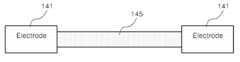
또한, 전압 제어부(160)는 스테이지(150)에 고정되어 상기 전도성 잉크를 토출하는 노즐(130)에 직류 전압(DC Voltage)을 인가하여, 도 2 및 도 3에 도시된 바와 같이 기판(140) 상에 전도성 잉크(145)를 선형(line type)으로 도포하며, 이때 인가되는 전압은 도 4에 도시된 바와 같이 직류 전압을 인가한다.2 and 3, the
도 2는 선형으로 전도성 잉크(145)를 도포한 단면도를 도시하고 있으며, 도 3은 전도성 잉크(145)를 도포한 상면도를 도시하고 있으며, 도 2 및 도 3에 도시된 바와 같이 상기 선형의 전도성 잉크(145)는 전극(141)과 전극(141)을 연결하도록 도포된다.Fig. 2 shows a cross-sectional view in which the
이때, 상기 전압 제어부(160)가 상기 기판(140) 상에 전도성 잉크(145)를 선형으로 도포시에는, 이동 제어부(165)가 상기 스테이지(150)를 수직으로 이동시켜 상기 기판에 상기 노즐을 최초 위치보다 근접하여 상기 전도성 잉크(145)를 도포할 수 있다.At this time, when the
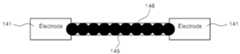
이후에는, 도 5 및 도 6에 도시된 바와 같이, 상기 전압 제어부(160)가 상기 노즐(130)에 펄스 전압(Pulse Voltage)을 인가하여 상기 선형으로 도포된 전도성 잉크(145) 상에 상기 전도성 잉크(146)를 드롭형(drop type)으로 도포하며, 이때 인가되는 전압은 도 8에 도시된 바와 같이 펄스 전압을 인가한다.5 and 6, the
도 5는 드롭형으로 전도성 잉크(165)를 도포한 단면도를 도시하고 있으며, 도 3은 전도성 잉크(146)를 도포한 상면도를 도시하고 있으며, 도 2 및 도 3에 도시된 바와 같이 상기 드롭형의 전도성 잉크(146)는 전극(141)과 전극(141)을 연결하되, 상기 선형 전도성 잉크(145) 상에 도포된다.FIG. 5 shows a cross-sectional view in which
이때, 상기 전압 제어부(160)가 상기 선형으로 도포된 전도성 잉크(145) 상에 상기 전도성 잉크(146)를 드롭 형으로 도포 시에는, 이동 제어부(165)가 상기 스테이지(150)를 수직으로 이동시켜 상기 전도성 잉크를 선형으로 도포시 보다 이격시켜 드롭형의 전도성 잉크(146)를 도포할 수 있다.At this time, when the
또한, 본 발명의 일실시예에 따르면, 상기와 같이 도포된 드롭형의 전도성 잉크(146) 상에 추가적으로 드롭형의 전도성 잉크를 도포하여 보다 두꺼운 전도성 잉크(146) 층을 구성하도록 할 수도 있다.
In addition, according to one embodiment of the present invention, a drop-type conductive ink may be further applied on the drop-type
도 9는 본 발명의 일실시예에 따른 전도성 잉크를 사용하는 디스플레이 수리 장치 및 방법의 동작 원리를 설명하기 위한 도면이다.9 is a view for explaining the operation principle of a display repairing apparatus and method using conductive ink according to an embodiment of the present invention.
도 9를 참조하여 본 발명의 일실시예에 따른 전도성 잉크를 사용하는 디스플레이 수리 장치 및 방법의 동작 원리를 보다 상세하게 설명하기로 한다.The operation principle of the display repair apparatus and method using the conductive ink according to an embodiment of the present invention will be described in detail with reference to FIG.
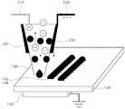
압력 제어부(120)가 일정한 압력(210)을 가하고, 전압 제어부(160)가 전압(220)을 가하면, 극성 용매(polarized solvent: 231)와 전도성 금속 재료(232)가 노즐(130)을 통하여 토출된다.The polarized solvent 231 and the
상기 극성 용매(231)는 음극(-)을 띄며, 상기 전도성 금속 재료(232)는 은(Ag)과 같은 금속 재료로 구성되며 양극(+)을 띄게된다.The polar solvent 231 has a negative (-) side, and the
따라서, 상기 전압 제어부(160)가 상기 노즐(130)에 직류 전압(DC Voltage)을 인가하면 스테이지(150) 상의 기판(140)에 전도성 잉크(145)를 선형(line type)으로 도포하며, 상기 노즐(130)에 펄스 전압(Pulse Voltage)을 인가하면 상기 선형으로 도포된 전도성 잉크 상(145)에 상기 전도성 잉크(146)를 드롭 형(drop type)으로 도포할 수 있다.
Accordingly, when the DC voltage is applied to the
도 10 내지 도 13은 본 발명의 일실시예에 따른 전도성 잉크를 사용하는 디스플레이 수리 장치 및 방법에 따른 전도성 잉크의 도포 결과를 설명하기 위한 도면이다.FIGS. 10 to 13 are views for explaining the results of application of the conductive ink according to the display repair apparatus and method using the conductive ink according to an embodiment of the present invention.
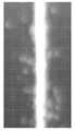
보다 상세하게 설명하면, 도 10 및 도 12는 종래 기술에 따른 전도성 잉크를 도포 결과를 도시한 도면이고, 도 13은 본 발명의 일실시예에 따른 전도성 잉크를 도포 결과를 도시한 도면이다.More specifically, FIGS. 10 and 12 show results of application of the conductive ink according to the prior art, and FIG. 13 illustrates the results of applying the conductive ink according to an embodiment of the present invention.
기판 상에 전도성 잉크를 드롭 형(drop type)으로 도포하는 경우에는 도 10에 도시된 바와 같이 전도성 잉크의 스프레이(spray) 현상이 발생한다.When the conductive ink is applied in a drop type on the substrate, a spray phenomenon of the conductive ink occurs as shown in FIG.
이는 전도성 잉크의 도포시에 전기장(electric field)에 의해 발생하는 현상으로 기판 상에 전도성 잉크를 드롭 형(drop type)으로 1회 도포하는 경우에는, 도 10에 도시된 바와 같이 스프레이 현상이 발생한다.This is a phenomenon caused by an electric field when the conductive ink is applied, and when the conductive ink is applied once in a drop type on the substrate, a spray phenomenon occurs as shown in FIG. 10 .
이와 같은 스프레이 현상을 보완하기 위하여, 기판 상에 전도성 잉크를 드롭 형(drop type)으로 5회 도포하는 경우에는, 도 11에 도시된 바와 같이 전도성 잉크가 도포되는 첫 지점에서 전도성 잉크가 쏟아지게 되어 일부 구간의 폭이 두꺼워지는 문제점이 발생하며, 전도성 잉크의 드롭이 균일하지 않아 단절되는 구간이 발생할 수 있다.In order to compensate for such a spray phenomenon, when the conductive ink is applied in a drop type five times on the substrate, the conductive ink is poured at the first point where the conductive ink is applied as shown in FIG. 11 There arises a problem that the width of a certain section becomes thick, and a section where the drop of the conductive ink is not uniform and is disconnected may occur.
이와 같은 전도성 잉크의 스프레이 현상과 단절 구간을 보완하기 위하여, 같이 기판 상에 전도성 잉크를 드롭 형(drop type)으로 10회 도포하는 경우에는, 도 11에 도시된 바와 같이 전도성 잉크의 퍼짐 현상이 발생하는 문제점이 있었다.In order to compensate for the spraying phenomenon and the cut-off period of the conductive ink, when the conductive ink is applied 10 times in a drop type on the substrate, spreading of the conductive ink occurs as shown in FIG. 11 .
그러나, 본 발명의 일실시예에서와 같이, 기판에 전도성 잉크를 선형(line type)으로 도포하고, 상기 선형으로 도포된 전도성 잉크 상에 상기 전도성 잉크를 드롭 형(drop type)으로 도포하는 경우에는, 도 13에 도시된 바와 같이 도포된 전도성 잉크의 스프레이 현상, 단절 구간 또는 퍼짐 현상이 발생하지 않는다.However, as in the embodiment of the present invention, when the conductive ink is applied to the substrate in a line type and the conductive ink is applied in a drop type on the linearly applied conductive ink, , The spraying phenomenon, the cut-off section, or the spreading phenomenon of the applied conductive ink does not occur as shown in Fig.
따라서, 본 발명의 실시예에 따르면 디스플레이 패널의 오픈 결함(open defect)의 수리를 위한 전도성 잉크의 토출(jetting) 시에 결함 없는 와이어링(wiring)이 가능하다.Therefore, according to the embodiment of the present invention, defectless wiring is possible when jetting the conductive ink for repairing an open defect of a display panel.
또한, 본 발명의 실시예에 따르면 전도성 잉크의 스프레이 현상, 단절 구간 또는 퍼짐 현상이 발생하지 않도록 하면서도 최소 선폭 1㎛의 구현이 가능하다.In addition, according to the embodiment of the present invention, it is possible to realize a minimum line width of 1 mu m while preventing the spraying phenomenon, the cut-off period, or the spreading phenomenon of the conductive ink.
전술한 바와 같은 본 발명의 상세한 설명에서는 구체적인 실시예에 관해 설명하였다. 그러나 본 발명의 범주에서 벗어나지 않는 한도 내에서는 여러 가지 변형이 가능하다. 본 발명의 기술적 사상은 본 발명의 전술한 실시예에 국한되어 정해져서는 안 되며, 특허청구범위뿐만 아니라 이 특허청구범위와 균등한 것들에 의해 정해져야 한다.In the foregoing detailed description of the present invention, specific examples have been described. However, various modifications are possible within the scope of the present invention. The technical spirit of the present invention should not be limited to the above-described embodiments of the present invention, but should be determined by the claims and equivalents thereof.
110: 잉크 저장부
120: 압력 제어부
130: 노즐
141: 전극
145: 선형 전도성 잉크
146: 드롭형 전도성 잉크
150: 스테이지
160: 전압 제어부
165: 이동 제어부
180: 레이저 다이오드
185: 레이저 위치 센서110:
120:
130: nozzle
141: Electrode
145: Linear conductive ink
146: drop type conductive ink
150: stage
160:
165:
180: laser diode
185: Laser position sensor
Claims (10)
Translated fromKorean상기 전도성 잉크를 토출시키는 노즐;
상기 토출된 전도성 잉크가 도포되는 기판이 배치되는 스테이지;
상기 노즐에 직류 전압(DC Voltage)을 인가하여 상기 기판 상에 전도성 잉크를 선형(line type)으로 도포하고, 상기 노즐에 펄스 전압(Pulse Voltage)을 인가하여 상기 선형으로 도포된 전도성 잉크 상에 상기 전도성 잉크를 드롭형(drop type)으로 도포하는 전압 제어부; 및
상기 스테이지를 수평 또는 수직으로 이동시키는 이동 제어부;
를 포함하고,
상기 전압 제어부가 상기 기판 상에 전도성 잉크를 선형으로 도포시에는, 상기 이동 제어부가 상기 스테이지를 수직으로 이동시켜 상기 기판에 상기 노즐을 최초 위치보다 근접시키고,
상기 전압 제어부가 상기 선형으로 도포된 전도성 잉크 상에 상기 전도성 잉크를 드롭형으로 도포 시에는, 상기 이동 제어부가 상기 스테이지를 수직으로 이동시켜 상기 전도성 잉크를 선형으로 도포시 보다 이격시키는 전도성 잉크를 사용하는 디스플레이 수리 장치.A pressure control unit for supplying the conductive ink by applying pressure to the ink storage unit in which the conductive ink is stored;
A nozzle for discharging the conductive ink;
A stage on which a substrate to which the discharged conductive ink is to be applied is disposed;
Applying a DC voltage to the nozzle to apply a conductive ink on the substrate in a line type and applying a pulse voltage to the nozzle to form a conductive ink on the linearly applied conductive ink, A voltage controller for applying the conductive ink in a drop type; And
A movement controller for moving the stage horizontally or vertically;
Lt; / RTI >
Wherein when the voltage control unit linearly applies the conductive ink on the substrate, the movement control unit moves the stage vertically to bring the nozzle closer to the substrate than the initial position,
When the voltage control unit applies the conductive ink in a drop shape onto the linearly coated conductive ink, the movement control unit moves the stage vertically to use the conductive ink that separates the conductive ink from the linearly applied coating ink Display repair device.
상기 기판과 상기 노즐 사이의 거리를 측정하는 레이저 거리 측정 장치;
를 더 포함하는 전도성 잉크를 사용하는 디스플레이 수리 장치.The method according to claim 1,
A laser distance measuring device for measuring a distance between the substrate and the nozzle;
Further comprising a conductive ink.
상기 레이저 거리 측정 장치는,
레이저를 출사시키는 레이저 다이오드; 및
상기 출사된 레이저를 수신하여 상기 기판과 상기 노즐 사이의 거리를 측정하는 레이저 위치 센서;
를 더 포함하는 전도성 잉크를 사용하는 디스플레이 수리 장치.The method of claim 4,
The laser distance measuring apparatus includes:
A laser diode for emitting a laser; And
A laser position sensor for receiving the emitted laser and measuring a distance between the substrate and the nozzle;
Further comprising a conductive ink.
상기 전도성 잉크는,
극성 용매(polarized solvent)와 전도성 금속 재료를 포함하는 전도성 잉크를 사용하는 디스플레이 수리 장치.The method according to claim 1,
Wherein the conductive ink comprises:
A display repair apparatus using a conductive ink comprising a polarized solvent and a conductive metal material.
상기 전도성 잉크는,
전극과 전극을 연결하는 전도성 잉크를 사용하는 디스플레이 수리 장치.The method according to claim 1,
Wherein the conductive ink comprises:
A display repair apparatus using conductive ink to connect electrodes and electrodes.
전압 제어부가 스테이지에 고정되어 상기 전도성 잉크를 토출하는 노즐에 직류 전압(DC Voltage)을 인가하여 기판 상에 전도성 잉크를 선형(line type)으로 도포하는 제2 단계; 및
상기 전압 제어부가 상기 노즐에 펄스 전압(Pulse Voltage)을 인가하여 상기 선형으로 도포된 전도성 잉크 상에 상기 전도성 잉크를 드롭형(drop type)으로 도포하는 제3 단계;
를 포함하고,
상기 제2 단계는,
상기 전압 제어부가 상기 기판 상에 전도성 잉크를 선형으로 도포시에는, 이동 제어부가 상기 스테이지를 수직으로 이동시켜 상기 기판에 상기 노즐을 최초 위치보다 근접시키고,
상기 제3 단계는,
상기 전압 제어부가 상기 선형으로 도포된 전도성 잉크 상에 상기 전도성 잉크를 드롭형으로 도포 시에는, 이동 제어부가 상기 스테이지를 수직으로 이동시켜 상기 전도성 잉크를 선형으로 도포시 보다 이격시켜 도포하는 전도성 잉크를 사용하는 디스플레이 수리 방법.
A first step of supplying a conductive ink by applying pressure to an ink storage part where a pressure control part stores conductive ink;
A second step of applying a direct current voltage (DC voltage) to a nozzle which is fixed to the stage and discharges the conductive ink to apply the conductive ink on the substrate in a line type; And
A third step of applying a pulse voltage to the nozzle to apply the conductive ink in a drop type on the linearly coated conductive ink;
Lt; / RTI >
The second step comprises:
When the voltage control unit linearly applies the conductive ink on the substrate, the movement control unit vertically moves the stage so that the nozzle is brought closer to the substrate than the initial position,
In the third step,
When the voltage control unit applies the conductive ink dropwise onto the linearly coated conductive ink, the movement control unit vertically moves the stage to apply the conductive ink to the conductive ink, How to repair your display.
Priority Applications (4)
| Application Number | Priority Date | Filing Date | Title |
|---|---|---|---|
| KR1020140111210AKR101549672B1 (en) | 2014-08-26 | 2014-08-26 | Display reparing device and method using conductive ink |
| CN201580045984.8ACN106794477B (en) | 2014-08-26 | 2015-03-25 | Display repair apparatus and method using conductive ink |
| PCT/KR2015/002934WO2016032081A1 (en) | 2014-08-26 | 2015-03-25 | Apparatus and method for repairing display using conductive ink |
| TW104113638ATWI609610B (en) | 2014-08-26 | 2015-04-29 | Display repairing device and method |
Applications Claiming Priority (1)
| Application Number | Priority Date | Filing Date | Title |
|---|---|---|---|
| KR1020140111210AKR101549672B1 (en) | 2014-08-26 | 2014-08-26 | Display reparing device and method using conductive ink |
Publications (1)
| Publication Number | Publication Date |
|---|---|
| KR101549672B1true KR101549672B1 (en) | 2015-09-03 |
Family
ID=54247083
Family Applications (1)
| Application Number | Title | Priority Date | Filing Date |
|---|---|---|---|
| KR1020140111210AActiveKR101549672B1 (en) | 2014-08-26 | 2014-08-26 | Display reparing device and method using conductive ink |
Country Status (4)
| Country | Link |
|---|---|
| KR (1) | KR101549672B1 (en) |
| CN (1) | CN106794477B (en) |
| TW (1) | TWI609610B (en) |
| WO (1) | WO2016032081A1 (en) |
Cited By (2)
| Publication number | Priority date | Publication date | Assignee | Title |
|---|---|---|---|---|
| WO2021085828A1 (en)* | 2019-10-29 | 2021-05-06 | 삼성디스플레이 주식회사 | Panel repairing device and panel repairing method |
| KR20210100228A (en) | 2020-01-28 | 2021-08-17 | 주식회사 코윈디에스티 | Method for repairing display panel and structure of display panel using thereof |
Citations (3)
| Publication number | Priority date | Publication date | Assignee | Title |
|---|---|---|---|---|
| JP2001088306A (en) | 1999-09-24 | 2001-04-03 | Dainippon Printing Co Ltd | Method of depositing liquid with specific electric conductivity by electric field jet |
| JP2006261228A (en)* | 2005-03-15 | 2006-09-28 | Kitakyushu Foundation For The Advancement Of Industry Science & Technology | Circuit board wiring pattern forming apparatus and wiring pattern repairing method |
| KR101425855B1 (en) | 2013-02-21 | 2014-08-14 | 서울대학교산학협력단 | Electroconductive ink composite including metal-organic precursor and method for Forming the metal line using the same |
Family Cites Families (6)
| Publication number | Priority date | Publication date | Assignee | Title |
|---|---|---|---|---|
| JP3975272B2 (en)* | 2002-02-21 | 2007-09-12 | 独立行政法人産業技術総合研究所 | Ultrafine fluid jet device |
| JP3967296B2 (en)* | 2003-08-08 | 2007-08-29 | シャープ株式会社 | Electrostatic suction type fluid discharge method and apparatus |
| CN100399152C (en)* | 2006-02-27 | 2008-07-02 | 友达光电股份有限公司 | Method for repairing transparent conductive layer and structure thereof |
| JP4018120B2 (en)* | 2006-05-12 | 2007-12-05 | シャープ株式会社 | Droplet discharge drawing device |
| CN101493586A (en)* | 2008-01-25 | 2009-07-29 | 东捷科技股份有限公司 | Pixel Repair System |
| US9198299B2 (en)* | 2012-12-11 | 2015-11-24 | Sharp Laboratories Of America, Inc. | Electrohydrodynamic (EHD) printing for the defect repair of contact printed circuits |
- 2014
- 2014-08-26KRKR1020140111210Apatent/KR101549672B1/enactiveActive
- 2015
- 2015-03-25CNCN201580045984.8Apatent/CN106794477B/enactiveActive
- 2015-03-25WOPCT/KR2015/002934patent/WO2016032081A1/enactiveApplication Filing
- 2015-04-29TWTW104113638Apatent/TWI609610B/enactive
Patent Citations (3)
| Publication number | Priority date | Publication date | Assignee | Title |
|---|---|---|---|---|
| JP2001088306A (en) | 1999-09-24 | 2001-04-03 | Dainippon Printing Co Ltd | Method of depositing liquid with specific electric conductivity by electric field jet |
| JP2006261228A (en)* | 2005-03-15 | 2006-09-28 | Kitakyushu Foundation For The Advancement Of Industry Science & Technology | Circuit board wiring pattern forming apparatus and wiring pattern repairing method |
| KR101425855B1 (en) | 2013-02-21 | 2014-08-14 | 서울대학교산학협력단 | Electroconductive ink composite including metal-organic precursor and method for Forming the metal line using the same |
Cited By (3)
| Publication number | Priority date | Publication date | Assignee | Title |
|---|---|---|---|---|
| WO2021085828A1 (en)* | 2019-10-29 | 2021-05-06 | 삼성디스플레이 주식회사 | Panel repairing device and panel repairing method |
| US12360408B2 (en) | 2019-10-29 | 2025-07-15 | Samsung Display Co., Ltd. | Panel repairing device and panel repairing method |
| KR20210100228A (en) | 2020-01-28 | 2021-08-17 | 주식회사 코윈디에스티 | Method for repairing display panel and structure of display panel using thereof |
Also Published As
| Publication number | Publication date |
|---|---|
| TW201607775A (en) | 2016-03-01 |
| WO2016032081A1 (en) | 2016-03-03 |
| CN106794477B (en) | 2019-12-13 |
| TWI609610B (en) | 2017-12-21 |
| CN106794477A (en) | 2017-05-31 |
Similar Documents
| Publication | Publication Date | Title |
|---|---|---|
| CA2741925C (en) | Improvements relating to additive manufacturing processes | |
| TWI569883B (en) | Electrostatic coating method and electrostatic coating device | |
| JP6268769B2 (en) | Method for forming conductive thin wire and wire and substrate used therefor | |
| JP2011119142A (en) | Method for manufacturing transparent conductive base material | |
| KR101454106B1 (en) | Apparatus and Method for forming pattern line by electrohydrodynamics | |
| CN100541273C (en) | Method for repairing defective portion in flat display panel | |
| KR101549672B1 (en) | Display reparing device and method using conductive ink | |
| TWI716587B (en) | Forming apparatus for pattern line | |
| JP2009113033A (en) | Apparatus for forming circuit on resin molded article having three-dimensional shape | |
| KR100963222B1 (en) | Inkjet Printing Apparatus, System and Method Using Roll | |
| JP2012135704A (en) | Electrospray deposition device | |
| Son et al. | Fine metal line patterning on hydrophilic non-conductive substrates based on electrohydrodynamic printing and laser sintering | |
| KR101632637B1 (en) | Display reparing device and method using conductive ink | |
| CN106229259A (en) | The preparation method that a kind of thin film transistor (TFT) prints electrode | |
| KR101323763B1 (en) | Apparatus for manufacturing printed transparent conductive electrode film | |
| TWI850746B (en) | Printed product, preparation method therefor, and use thereof | |
| KR101501123B1 (en) | Slot-die coating method and apparatus for making thin-film | |
| KR20100110982A (en) | Pattern method using inkjet printing | |
| Prakasan et al. | In-Situ and Simultaneous Surface Treatment and Self-Sintering of Patterned Conductive Traces | |
| JP2015003293A (en) | Electrostatic spray film production method and electrostatic spray film production device | |
| KR101442672B1 (en) | Spray nozzle system using mask and method for fabricating touch screen for the same | |
| JP2015185418A (en) | Method of estimating thin film for organic el element and thin film forming apparatus for organic el element | |
| KR100754675B1 (en) | Pattern forming apparatus and manufacturing apparatus using the same | |
| JP2016137461A (en) | Electrospray coating device | |
| Son et al. | Fine metal line patterning of ITO ink based on electrohydrodynamic printing |
Legal Events
| Date | Code | Title | Description |
|---|---|---|---|
| PA0109 | Patent application | St.27 status event code:A-0-1-A10-A12-nap-PA0109 | |
| PA0201 | Request for examination | St.27 status event code:A-1-2-D10-D11-exm-PA0201 | |
| D13-X000 | Search requested | St.27 status event code:A-1-2-D10-D13-srh-X000 | |
| D14-X000 | Search report completed | St.27 status event code:A-1-2-D10-D14-srh-X000 | |
| PE0902 | Notice of grounds for rejection | St.27 status event code:A-1-2-D10-D21-exm-PE0902 | |
| E13-X000 | Pre-grant limitation requested | St.27 status event code:A-2-3-E10-E13-lim-X000 | |
| P11-X000 | Amendment of application requested | St.27 status event code:A-2-2-P10-P11-nap-X000 | |
| P13-X000 | Application amended | St.27 status event code:A-2-2-P10-P13-nap-X000 | |
| PE0701 | Decision of registration | St.27 status event code:A-1-2-D10-D22-exm-PE0701 | |
| GRNT | Written decision to grant | ||
| PR0701 | Registration of establishment | St.27 status event code:A-2-4-F10-F11-exm-PR0701 | |
| PR1002 | Payment of registration fee | St.27 status event code:A-2-2-U10-U11-oth-PR1002 Fee payment year number:1 | |
| PG1601 | Publication of registration | St.27 status event code:A-4-4-Q10-Q13-nap-PG1601 | |
| FPAY | Annual fee payment | Payment date:20180927 Year of fee payment:4 | |
| PR1001 | Payment of annual fee | St.27 status event code:A-4-4-U10-U11-oth-PR1001 Fee payment year number:4 | |
| R18-X000 | Changes to party contact information recorded | St.27 status event code:A-5-5-R10-R18-oth-X000 | |
| FPAY | Annual fee payment | Payment date:20190827 Year of fee payment:5 | |
| PR1001 | Payment of annual fee | St.27 status event code:A-4-4-U10-U11-oth-PR1001 Fee payment year number:5 | |
| PN2301 | Change of applicant | St.27 status event code:A-5-5-R10-R13-asn-PN2301 St.27 status event code:A-5-5-R10-R11-asn-PN2301 | |
| PR1001 | Payment of annual fee | St.27 status event code:A-4-4-U10-U11-oth-PR1001 Fee payment year number:6 | |
| R18-X000 | Changes to party contact information recorded | St.27 status event code:A-5-5-R10-R18-oth-X000 | |
| PR1001 | Payment of annual fee | St.27 status event code:A-4-4-U10-U11-oth-PR1001 Fee payment year number:7 | |
| PR1001 | Payment of annual fee | St.27 status event code:A-4-4-U10-U11-oth-PR1001 Fee payment year number:8 | |
| R18-X000 | Changes to party contact information recorded | St.27 status event code:A-5-5-R10-R18-oth-X000 | |
| PN2301 | Change of applicant | St.27 status event code:A-5-5-R10-R13-asn-PN2301 St.27 status event code:A-5-5-R10-R11-asn-PN2301 | |
| PR1001 | Payment of annual fee | St.27 status event code:A-4-4-U10-U11-oth-PR1001 Fee payment year number:9 | |
| PR1001 | Payment of annual fee | St.27 status event code:A-4-4-U10-U11-oth-PR1001 Fee payment year number:10 | |
| PR1001 | Payment of annual fee | St.27 status event code:A-4-4-U10-U11-oth-PR1001 Fee payment year number:11 |