KR101547076B1 - Daisy chain cascading devices - Google Patents
Daisy chain cascading devicesDownload PDFInfo
- Publication number
- KR101547076B1 KR101547076B1KR1020147013416AKR20147013416AKR101547076B1KR 101547076 B1KR101547076 B1KR 101547076B1KR 1020147013416 AKR1020147013416 AKR 1020147013416AKR 20147013416 AKR20147013416 AKR 20147013416AKR 101547076 B1KR101547076 B1KR 101547076B1
- Authority
- KR
- South Korea
- Prior art keywords
- output
- memory device
- input
- data
- memory
- Prior art date
- Legal status (The legal status is an assumption and is not a legal conclusion. Google has not performed a legal analysis and makes no representation as to the accuracy of the status listed.)
- Expired - Fee Related
Links
Images


Classifications
- G—PHYSICS
- G11—INFORMATION STORAGE
- G11C—STATIC STORES
- G11C7/00—Arrangements for writing information into, or reading information out from, a digital store
- G11C7/10—Input/output [I/O] data interface arrangements, e.g. I/O data control circuits, I/O data buffers
- G—PHYSICS
- G06—COMPUTING OR CALCULATING; COUNTING
- G06F—ELECTRIC DIGITAL DATA PROCESSING
- G06F13/00—Interconnection of, or transfer of information or other signals between, memories, input/output devices or central processing units
- G06F13/14—Handling requests for interconnection or transfer
- G—PHYSICS
- G06—COMPUTING OR CALCULATING; COUNTING
- G06F—ELECTRIC DIGITAL DATA PROCESSING
- G06F13/00—Interconnection of, or transfer of information or other signals between, memories, input/output devices or central processing units
- G06F13/38—Information transfer, e.g. on bus
- G06F13/42—Bus transfer protocol, e.g. handshake; Synchronisation
- G06F13/4247—Bus transfer protocol, e.g. handshake; Synchronisation on a daisy chain bus
- G06F13/4256—Bus transfer protocol, e.g. handshake; Synchronisation on a daisy chain bus using a clocked protocol
- G—PHYSICS
- G11—INFORMATION STORAGE
- G11C—STATIC STORES
- G11C5/00—Details of stores covered by group G11C11/00
- G11C5/06—Arrangements for interconnecting storage elements electrically, e.g. by wiring
- G11C5/066—Means for reducing external access-lines for a semiconductor memory clip, e.g. by multiplexing at least address and data signals
- G—PHYSICS
- G11—INFORMATION STORAGE
- G11C—STATIC STORES
- G11C7/00—Arrangements for writing information into, or reading information out from, a digital store
- G11C7/22—Read-write [R-W] timing or clocking circuits; Read-write [R-W] control signal generators or management
- G—PHYSICS
- G06—COMPUTING OR CALCULATING; COUNTING
- G06F—ELECTRIC DIGITAL DATA PROCESSING
- G06F12/00—Accessing, addressing or allocating within memory systems or architectures
- G06F12/02—Addressing or allocation; Relocation
- G06F12/06—Addressing a physical block of locations, e.g. base addressing, module addressing, memory dedication
- G06F12/0615—Address space extension
- G06F12/0623—Address space extension for memory modules
- G—PHYSICS
- G11—INFORMATION STORAGE
- G11C—STATIC STORES
- G11C16/00—Erasable programmable read-only memories
- G11C16/02—Erasable programmable read-only memories electrically programmable
- G11C16/06—Auxiliary circuits, e.g. for writing into memory
Landscapes
- Engineering & Computer Science (AREA)
- Theoretical Computer Science (AREA)
- Physics & Mathematics (AREA)
- General Engineering & Computer Science (AREA)
- General Physics & Mathematics (AREA)
- Bus Control (AREA)
- Information Transfer Systems (AREA)
- Dram (AREA)
- Memory System (AREA)
- Read Only Memory (AREA)
- Small-Scale Networks (AREA)
Abstract
Translated fromKorean
Description
Translated fromKorean본 발명은 데이지 체인 케스케이딩 장치에 관한 것이다.The present invention relates to daisy chain cascading devices.
현재의 컴퓨터 기반 시스템들은 거의 어디에서나 찾아볼 수 있고, 셀 폰, 휴대용 컴퓨터, 자동차, 의료 장치, 퍼스널 컴퓨터 등과 같은 매일 사회적으로 사용되는 다수의 장치로의 진출이 행해져 왔다. 일반적으로, 체크북(checkbook)의 밸런싱(balancing) 같은 간단한 태스크(task)와 같은 일상의 태스크 내지 날씨를 예측하는 것과 같은 비교적 복잡한 태스크를 다루기 위해 컴퓨터 기반 시스템에 매우 의존하는 사회가 존재해왔다. 기술이 향상됨에 따라, 더욱 많은 태스크가 컴퓨터 기반 시스템으로 이동된다. 이것은 차례로, 사회가 더욱더 이들 시스템에 의존하게 되도록 한다.Current computer-based systems can be found almost anywhere and have been made into a number of socially used devices, such as cell phones, portable computers, automobiles, medical devices, personal computers, and the like. In general, there have been societies that rely heavily on computer-based systems to handle relatively complex tasks such as predicting everyday tasks or weather, such as simple tasks such as balancing a checkbook. As technology improves, more tasks are moved to computer-based systems. This, in turn, makes society more dependent on these systems.
전형적인 컴퓨터 기반 시스템은 시스템 보드, 및 옵션으로 디스플레이 유닛, 저장 유닛 등과 같은 하나 이상의 주변 장치를 포함한다. 시스템 보드는 하나 이상의 프로세서, 메모리 서브시스템, 및 직렬 장치 인터페이스, 네트워크 장치 제어기, 하드 디스크 제어기 등과 같은 다른 로직을 포함할 수 있다.A typical computer-based system includes a system board, and optionally one or more peripheral devices such as a display unit, a storage unit, and the like. The system board may include one or more processors, memory subsystems, and other logic such as a serial device interface, a network device controller, a hard disk controller, and the like.
특정 시스템 보드에 채용되는 프로세스의 타입은 일반적으로, 시스템에 의해 실행되는 태스크의 타입에 의존한다. 예를 들면, 자동차 엔진에 의해 생성되는 배출물을 모니터하고 엔진이 연료를 완전히 연소되게 하도록 공기/연료 혼합물을 조정하는 것과 같은 제한된 세트의 태스크를 실행하는 시스템은, 이들 태스크를 실행하는 데 맞추어진 간단한 특정화된 프로세서를 채용할 수 있다. 한편, 다수의 사용자를 관리하고 다수의 상이한 애플리케이션을 실행하는 것과 같은 다수의 상이한 태스크를 실행하는 시스템은, 고속 계산을 실행하고 사용자의 요구에 대해 서비스하는 응답 시간을 최소화하도록 데이터를 조작하게끔 구성된, 사실상 범용인 하나 이상의 복잡한 프로세서를 채용할 수 있다.The type of process employed on a particular system board generally depends on the type of task being executed by the system. For example, a system that implements a limited set of tasks, such as monitoring emissions produced by an automotive engine and adjusting the air / fuel mixture to cause the engine to fully combust the fuel, A specified processor can be employed. On the other hand, a system that executes a number of different tasks, such as managing a large number of users and executing a number of different applications, is configured to manipulate data to perform high-speed computations and minimize response time servicing the user & It is possible to employ one or more complex processors which are generally universal.
메모리 서브시스템은 프로세서에 의해 사용되는 정보(예컨대, 지시, 데이터 값)을 유지하는 저장장치이다. 메모리 서브시스템은 일반적으로, 제어기 로직 및 하나 이상의 메모리 장치를 포함한다. 제어기 로직은 일반적으로, 프로세서들과 메모리 장치들을 인터페이스하여, 프로세서들이 메모리 장치들에/로부터 정보를 저장 및 검색하도록 인에이블시킨다. 메모리 장치는 실제의 정보를 유지한다.The memory subsystem is a storage device that holds information (e.g., instructions, data values) used by the processor. The memory subsystem typically includes controller logic and one or more memory devices. Controller logic generally interfaces processors and memory devices to enable processors to store and retrieve information to and from memory devices. The memory device maintains actual information.
프로세서와 같이, 메모리 서브시스템에 채용되는 장치들의 타입은 종종 컴퓨터 시스템에 의해 실행되는 태스크의 타입에 의해 도출된다. 예를 들면, 컴퓨터 시스템은 디스크 드라이브의 도움 없이 부트하여 변하지 않는 소프트웨어 루틴의 세트를 실행해야 하는 태스크를 가질 수 있다. 여기에서, 메모리 서브시스템은 플래시 메모리 장치와 같은 비휘발성 장치를 채용하여 소프트웨어 루틴을 저장할 수 있다. 다른 컴퓨터 시스템은 큰 부분의 정보를 유지하도록 대형 고속 데이터 저장장치를 필요로 하는 매우 복잡한 태스크를 실행할 수 있다. 여기에서, 메모리 서브시스템은 큰 부분의 정보를 저장하기 위해 고속 고밀도 동적 랜덤 액세스 메모리(DRAM)을 채용할 수도 있다.The type of devices employed in the memory subsystem, such as a processor, is often derived by the type of task being executed by the computer system. For example, a computer system may have a task to boot without assistance of a disk drive to execute a set of unchanging software routines. Here, the memory subsystem may employ non-volatile devices such as flash memory devices to store software routines. Other computer systems can perform very complex tasks that require large, high-speed data storage devices to maintain a large portion of information. Here, the memory subsystem may employ a high-speed, high-density dynamic random access memory (DRAM) to store a large portion of information.
현재, 하드 디스크 드라이브는 20∼40 기가바이트의 데이터를 저장할 수 있는 고밀도를 갖지만, 비교적 부피가 크다. 그러나, 고체 드라이브라고도 알려진 플래시 메모리는 하드 디스크 드라이브에 비해 고밀도, 비휘발성 및 작은 사이즈로 인해 인기가 있다. 플래시 메모리 기술은 EPROM 및 EEPROM 기술에 의거한다. 용어 "플래시"는 EEPROM와 구별되는 바와 같이 한번에 다수의 메모리 셀이 소거될 수 있기 때문에 선택되었으며, 각 바이트가 개별적으로 소거되었다. 멀티 레벨 셀(MLC)의 출현은 단일 레벨 셀에 비해 플래시 메모리 밀도를 더욱 증가시킨다. 당업자는 플래시 메모리가 NOR 플래시 또는 NAND 플래시로서 구성될 수 있음을 이해할 것이고, NAND 플래시가 더욱 간단한 메모리 어레이 구조로 인해 소정 면적당의 더 높은 밀도를 갖는다. 더욱 논의할 목적으로, 플래시 메모리에 대한 언급은 NOR 또는 NAND 또는 다른 타입의 플래시 메모리 어느 것으로서 이해되어야 한다.Currently, hard disk drives have a high density capable of storing 20 to 40 gigabytes of data, but are relatively bulky. However, flash memory, also known as a solid-state drive, is popular due to its high density, non-volatility and small size compared to hard disk drives. Flash memory technology is based on EPROM and EEPROM technology. The term "flash" has been selected because multiple memory cells can be erased at one time, as distinguished from EEPROM, and each byte has been individually erased. The emergence of multilevel cells (MLCs) further increases the flash memory density over single level cells. Those skilled in the art will appreciate that the flash memory may be configured as a NOR flash or NAND flash, and the NAND flash has a higher density per given area due to the simpler memory array architecture. For further discussion, references to flash memory should be understood as either NOR or NAND or any other type of flash memory.
메모리 서브시스템 내의 장치들은 종종, 병렬 상호접속 스킴(scheme)을 사용하여 상호접속된다. 이 스킴은 어드레스 및 데이터 정보 및 제어 신호들이 병렬식으로 장치들에 연결되는 방식으로 장치들을 상호접속하는 것을 포함한다. 각 장치는, 장치들로의 데이터 및 어드레스 정보뿐만 아니라 제어 신호의 병렬 전송을 조정하도록 복수의 입력/출력을 통합할 수 있다.Devices in a memory subsystem are often interconnected using a parallel interconnect scheme. This scheme involves interconnecting devices in such a way that address and data information and control signals are connected in parallel to the devices. Each device may incorporate a plurality of inputs / outputs to coordinate data and address information to devices as well as parallel transmission of control signals.
메모리 서브시스템에서 병렬 상호접속을 이용하는 것과 관련한 하나의 결점은 정보 및 신호들을 장치들에 병렬로 전송하기 위해 장치들 간에 다수의 상호접속이 필요한 경향이 있다는 것이다. 이것은 이들 서브시스템을 구현하는 보드의 복잡성을 더한다. 또한, 혼선과 같은 다수의 상호접속과 관련된 불필요한 영향이 이들 서브시스템의 성능을 제한하기 쉽다. 더욱이, 이들 서브시스템에 통합되어 있는 장치들의 수가 상호접속에 의해 반송되는 신호들의 전달 지연으로 인해 제한될 수도 있다.One drawback with using parallel interconnects in memory subsystems is that there is a need for multiple interconnections between devices to transfer information and signals to devices in parallel. This adds to the complexity of the board implementing these subsystems. In addition, unnecessary effects associated with multiple interconnections, such as cross talk, are likely to limit the performance of these subsystems. Moreover, the number of devices integrated in these subsystems may be limited due to the propagation delay of the signals carried by the interconnection.
여기에 설명한 기술들은 병렬 상호접속 구현예들보다 더 적고 더 짧은 접속을 채용하는 직렬 데이지 체인 캐스케이딩 배열로 장치들을 연결하는 기술을 제공함으로써 상기 결점을 극복한다. 데이지 체인 배열로 장치들을 구성하면, 더 적고 더 짧은 상호접속을 이용하는 것이 전체 구현을 전파 지연 및 혼선과 같은 불필요한 영향에 상처를 덜 받게 하기 때문에, 병렬 상호접속 구현예들보다 더 고속으로 장치들이 동작될 수 있게 할 수 있다. 또한, 더 적고 더 짧은 접속이 구현의 복잡성을 감소시키기 쉽다. 이러한 감소된 복잡성은 또한, 장치들을 포함하는 서브시스템이 더 작은 면적으로 구현되도록 인에이블시켜, 서브시스템이 더 작은 풋프린트를 점유하게 한다.The techniques described herein overcome this drawback by providing a technique for connecting devices with a serial daisy chain cascading arrangement that employs fewer and shorter connections than parallel interconnect implementations. When devices are configured in a daisy-chained arrangement, devices are operated at a higher speed than parallel interconnect implementations, because using fewer, shorter interconnects is less prone to unnecessary effects such as propagation delays and crosstalk, Can be done. Also, fewer and shorter connections are likely to reduce implementation complexity. This reduced complexity also enables the subsystem containing the devices to be implemented with a smaller footprint, allowing the subsystem to occupy a smaller footprint.
여기에 설명한 기술들의 양태에 따르면, 장치들이 데이지 체인 캐스케이드 배열로 연결되어, 데이지 체인 캐스케이드 내의 더 앞의 장치의 출력들이 데이지 체인 내의 더 뒤의 다음의 장치의 입력들에 연결되어, 더 앞의 장치로부터 더 뒤의 장치로의 정보(예컨대, 데이터, 어드레스 및 커맨드 정보) 및 제어 신호(예컨대, 인에이블 신호)의 전송을 조정한다.According to an aspect of the techniques described herein, the devices are connected in a daisy chain cascade arrangement such that the outputs of the earlier devices in the daisy chain cascade are connected to the inputs of the subsequent devices in the daisy chain, (E.g., data, address, and command information) and a control signal (e.g., an enable signal) to a later device.
기술들의 일 실시예에서, 데이지 체인 캐스케이드 내의 각 장치는 직렬 입력(SI) 및 직렬 출력(SO)을 포함한다. 정보가 장치의 SI를 통해 장치에 입력된다. 유사하게, 정보는 장치의 SO를 통해 장치로부터 출력된다. 데이지 체인 케스케이드 내의 장치의 SO는 데이지 체인 캐스케이드 내의 다음의 장치의 SI에 연결된다. 장치의 SI를 통해 데이지 체인 캐스케이드 내의 더 앞의 장치로 입력된 정보가 장치를 통과하여 장치의 SO를 통해 장치로부터 출력되도록 인에이블시키기 위해 장치들 내에 회로가 제공된다. 정보는 그 후 다음의 장치의 SI와 더 앞의 장치의 SO 사이의 접속을 통해 데이지 체인 캐스케이드 내의 다음의 SI에 전송된다. 전송된 정보는 장치의 SI를 통해 다음의 장치에 입력될 수도 있다.In one embodiment of the techniques, each device in the daisy chain cascade includes a serial input (SI) and a serial output (SO). Information is input to the device through the SI of the device. Similarly, information is output from the device via the SO of the device. The SO of the device in the daisy chain cascade is connected to the SI of the next device in the daisy chain cascade. Circuitry is provided within the devices to enable information input to a further device in a daisy-chain cascade via the SI of the device to be output from the device through the device's SO through the device. The information is then transmitted to the next SI in the daisy chain cascade via the connection between the SI of the next device and the SO of the previous device. The transmitted information may be input to the next device through the SI of the device.
또한, 클록 신호가 데이지 체인 캐스케이드 내의 장치들에 연결된다. 클록 신호는 데이지 체인 캐스케이드 내의 하나의 장치에서 다음의 장치로의 정보의 전송을 조정하도록 장치들에 의해 사용된다.Also, the clock signal is coupled to devices in a daisy chain cascade. The clock signal is used by devices to coordinate the transmission of information from one device to the next in a daisy chain cascade.
여기에 설명된 기술들의 다른 양태에 따르면, 예컨대, 데이터를 SI를 통해 장치에 입력되게 그리고 SO를 통해 장치로부터 출력되게 인에이블시키기 위해 장치에 의해 이용되는 제어 신호(예컨대, 인에이블 신호)가 상술한 바와 같이, 데이지 체인 캐스케이드 내의 장치들 간에 전송된다. 여기에서, 데이지 체인 캐스케이드 내의 더 앞의 장치로 입력된 제어 신호가 장치를 통해 전달되어 장치로부터 출력을 통해 데이지 체인 캐스케이드 내의 다음의 장치의 입력으로 전송되도록 인에이블시키기 위해 회로가 제공된다. 전송된 제어 신호는 그 후 입력을 통해 다음의 장치에 입력된다.According to another aspect of the techniques described herein, a control signal (e.g., an enable signal) used by the device to enable data to be input to the device via SI and to be output from the device via SO, As is done, it is transmitted between devices in a daisy chain cascade. Here, a circuit is provided for enabling a control signal input to a further device in a daisy-chain cascade to be transmitted through the device and transmitted from the device via the output to the input of the next device in the daisy-chain cascade. The transmitted control signal is then input to the next device via the input.
본 발명의 원리들에 따르면, 플래시 메모리 시스템이 복수의 직렬로 접속된 플래시 메모리 장치를 가질 수 있다. 그 시스템의 플래시 메모리 장치는 직렬 입력 데이터 포트 및 직렬 데이터 출력 포트를 갖는 직렬 데이터 링크 인터페이스, 제1 입력 인에이블 신호를 수신하는 제어 입력 포트, 및 제2 입력 인에이블 신호를 송신하는 제어 출력 포트를 포함할 수 있다. 입력 인에이블 신호는 직렬 데이터 링크 인터페이스와 메모리 뱅크 간의 데이터 전송을 제어하는 회로에 사용된다. 플래시 메모리 장치는 외부 소스로부터 직렬 입력 데이터 및 제어 신호를 수신하고, 외부 장치에 데이터 및 제어 신호를 제공하도록 구성된다. 외부 소스 및 외부 장치는 시스템 내의 다른 메모리 장치들일 수도 있다. 본 발명의 실시예에서는, 장치들이 시스템 내에서 직렬로 캐스케이드되어 있을 때, 그들 장치는 수신된 IPE 및 OPE 신호를 외부 장치로 "반향하는(echo)" 출력 제어 포트를 더 가질 수 있다. 이로 인해, 시스템이 데이지 체인 캐스케이딩 스킴(대 브로드캐스팅/멀티드롭 캐스케이딩 스킴)을 형성하도록 포인트간 접속된 신호 포트를 갖는다.According to the principles of the present invention, a flash memory system may have a plurality of serially connected flash memory devices. The flash memory device of the system includes a serial data link interface having a serial input data port and a serial data output port, a control input port for receiving a first input enable signal, and a control output port for transmitting a second input enable signal . The input enable signal is used in the circuit that controls the data transfer between the serial data link interface and the memory bank. The flash memory device is configured to receive serial input data and control signals from an external source and provide data and control signals to an external device. The external source and external device may be other memory devices in the system. In an embodiment of the invention, when the devices are cascaded in series within the system, they may further have an output control port echoing the received IPE and OPE signals to the external device. Thereby, the system has point-to-point connected signal ports to form a daisy-chained cascading scheme (large broadcasting / multi-drop cascading scheme).
이들 시스템은, 제한된 하드웨어 물리 장치 선택 핀들을 사용하는 것보다는, 전체 시스템이 시스템의 전체 성능을 희생하지 않고 메모리 밀도의 점에서 쉽게 가능한 많이 팽창할 수 있게 하기 위해, 고유 장치 식별 및 타깃 장치 선택 어드레스 스킴을 사용할 수 있다. 본 발명의 일부 실시예에서, 각각의 플래시 메모리 장치는 고유 장치 식별자를 포함할 수 있다. 장치들은 직렬 입력 데이터 내의 타깃 장치 정보 필드를 파싱(parsing)하여, 타깃 장치 정보와 장치의 고유 장치 식별 번호를 상관시켜 장치가 타깃 장치인지를 판정하도록 구성될 수 있다. 장치는 수신된 임의의 부가 입력 데이터를 처리하기 전에 타깃 장치 정보 필드를 파싱할 수도 있다. 메모리 장치가 타깃 장치가 아니면, 직렬 입력 데이터를 무시할 수 있으므로, 부가적인 처리 시간 및 자원을 절감할 수 있다.These systems require unique device identification and target device selection addressing to allow the entire system to expand as readily as possible in terms of memory density without sacrificing the overall performance of the system, rather than using limited hardware physical device select pins You can use schemes. In some embodiments of the invention, each flash memory device may include a unique device identifier. The devices may be configured to parse the target device information field in the serial input data to correlate the target device information and the unique device identification number of the device to determine whether the device is the target device. The device may parse the target device information field before processing any additional input data received. If the memory device is not the target device, the serial input data can be ignored, thereby saving additional processing time and resources.
이상의 설명은, 같은 참조 문자가 다른 도면에 걸쳐 동일한 부분을 언급하는 첨부하는 도면에 예시된 바와 같이, 발명의 아래의 예시적인 실시예의 더욱 특별한 설명으로부터 명백해질 것이다. 도면들은, 반드시 축소, 강조하기 위한 것은 아니고, 그 대신에 본 발명의 실시예들을 예시하기 위한 것이다.The foregoing description will become apparent from a more particular description of exemplary embodiments of the invention as illustrated in the accompanying drawings, wherein like reference characters refer to the same parts throughout the different views. The drawings are not necessarily to scale down or emphasize, but instead are for the purpose of illustrating embodiments of the invention.
도 1은 직렬 데이지 체인 캐스케이드 배열로 구성된 복수의 단일 포트 장치를 포함하는 예시적인 장치 구성의 블록도이다.
도 2는 캐스케이드된 클록을 갖는 직렬 데이지 체인 캐스케이드 배열로 구성된 복수의 단일 포트 장치를 포함하는 예시적인 장치 구성의 블록도이다.
도 3은 직렬 데이지 체인 캐스케이드 배열로 구성된 복수의 이중 포트 장치를 포함하는 예시적인 장치 구성의 블록도이다.
도 4는 여러 가지 인에이블 신호용의 입력 및 출력을 갖는 직렬 데이지 체인 배열로 구성된 복수의 단일 포트 장치를 포함하는 예시적인 장치 구성의 블록도이다.
도 5는 여러 가지 인에이블 신호용으로 구성된 입력 및 출력을 갖는 직렬 데이지 체인 배열로 구성된 이중 포트 장치를 포함하는 예시적인 장치 구성의 블록도이다.
도 6은 직렬 데이지 체인 캐스케이딩 배열로 구성되는 복수의 직렬 입력 및 복수의 직렬 출력을 갖는 복수의 장치를 포함하는 예시적인 장치 구성의 블록도이다.
도 7은 직렬 데이지 체인 캐스케이딩 배열로 구성된 단일 장치 및 그 배열로 구성된 복수의 장치에서 실행되는 판독 동작과 관련된 타이밍을 도시하는 타이밍도이다.
도 8은 직렬 데이지 체인 캐스케이딩 배열로 구성된 장치들 사이에서 전송되는 정보와 관련된 타이밍을 도시하는 타이밍도이다.
도 9는 단일 포트의 장치용의 예시적인 직렬 출력 제어 로직의 고 레벨 블록도이다.
도 10은 이중 포트의 장치용의 예시적인 직렬 출력 제어 로직의 고 레벨 블록도이다.
도 11은 장치용의 예시적인 직렬 출력 제어 로직의 상세한 블록도이다.
도 12는 직렬 데이지 체인 캐스케이딩 배열로 구성되고 예시적인 직렬 출력 제어 로직을 포함하는 장치들의 예시적인 구성의 블록도이다.
도 13은 예시적인 직렬 출력 제어 로직을 포함하는 장치들의 입력 및 출력과 관련된 타이밍을 도시하는 타이밍도이다.
도 14는 데이지 체인 캐스케이드 내의 제1 장치에 포함된 메모리로부터 데이지 체인 캐스케이드 내의 제2 장치로 데이터를 전송하는 데 사용될 수 있는 예시적인 직렬 출력 제어 로직의 블록도이다.
도 15는 예시적인 직렬 출력 제어 로직을 사용하여 데이지 체인 캐스케이드 내의 제1 장치의 메모리에 포함되는 데이터를 데이지 체인 캐스케이드 내의 제2 장치에 전송하는 것과 관련된 타이밍을 도시하는 타이밍도이다.1 is a block diagram of an exemplary device configuration including a plurality of single-port devices configured in a cascade arrangement in a serial daisy chain.
2 is a block diagram of an exemplary device configuration including a plurality of single port devices configured with a cascaded array of daisy chained cascaded clocks.
Figure 3 is a block diagram of an exemplary device configuration including a plurality of dual port devices configured in a cascade arrangement in a serial daisy chain.
4 is a block diagram of an exemplary device configuration including a plurality of single port devices configured in a serial daisy chain arrangement having input and output for various enable signals.
Figure 5 is a block diagram of an exemplary device configuration including a dual port device configured with a serial daisy chain arrangement having inputs and outputs configured for various enable signals.
6 is a block diagram of an exemplary device configuration including a plurality of devices having a plurality of serial inputs and a plurality of serial outputs configured in a serial daisy-chain cascading arrangement.
7 is a timing diagram illustrating the timing associated with a read operation performed on a single device configured with a serial daisy-chain cascading arrangement and a plurality of devices configured with the array.
8 is a timing diagram illustrating the timing associated with information transmitted between devices configured with a serial daisy-chain cascading arrangement.
9 is a high-level block diagram of an exemplary serial output control logic for a single port device.
10 is a high-level block diagram of an exemplary serial output control logic for a dual port device.
11 is a detailed block diagram of an exemplary serial output control logic for the device.
FIG. 12 is a block diagram of an exemplary configuration of devices configured with a serial daisy-chain cascading arrangement and including exemplary serial output control logic.
13 is a timing diagram illustrating the timing associated with the input and output of devices including the exemplary serial output control logic.
14 is a block diagram of an exemplary serial output control logic that may be used to transfer data from a memory included in a first device in a daisy chain cascade to a second device in a daisy chain cascade.
15 is a timing diagram illustrating the timing associated with transmitting data contained in a memory of a first device in a daisy chain cascade to a second device in a daisy chain cascade using the exemplary serial output control logic.
이하 본 발명의 바람직한 실시예를 설명한다.Hereinafter, preferred embodiments of the present invention will be described.
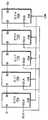
도 1은 직렬 데이지 체인 캐스케이드 배열로 구성된 복수의 단일 포트 장치들(110a∼e)을 포함하는 예시적인 장치 구성의 블록도이다. 장치들(110a∼e)은 동적 랜덤 액세스 메모리(DRAM) 셀, 정적 랜덤 액세스 메모리(SRAM) 셀, 플래시 메모리 셀 등을 포함할 수 있는 메모리(도시 생략)를 각각 포함하는 예시적인 메모리 장치들이다. 각 장치(110)는 직렬 입력(SI), 직렬 출력(SO), 클록(SCLK) 입력 및 칩 선택(CS#) 입력을 포함한다.FIG. 1 is a block diagram of an exemplary device configuration including a plurality of
SI는 정보(예컨대, 커맨드, 어드레스 및 데이터 정보)를 장치(110)에 전송하는 데 사용된다. SO는 장치(110)로부터 정보를 전송하는 데 사용된다. SCLK 입력은 외부 클록 신호를 장치(110)에 제공하는 데 사용되고, CS# 입력은 칩 선택 신호를 장치(110)에 제공하는 데 사용된다. 여기에서 설명하는 기술과 함께 사용될 수 있는 장치의 일례는 미국 특허 출원 11/324,023호에 기재되어 있는 복수의 독립 직렬 링크(MISL) 메모리 장치이다.The SI is used to transfer information (e.g., command, address, and data information) The SO is used to transfer information from the device 110. The SCLK input is used to provide an external clock signal to the device 110 and the CS # input is used to provide a chip select signal to the device 110. [ An example of a device that can be used with the techniques described herein is a plurality of independent serial link (MISL) memory devices as described in U.S. Patent Application 11 / 324,023.
SI 및 SO는 데이지 체인 캐스케이드 배열에서 장치들(110) 사이에 접속되어, 데이지 체인 캐스케이드에서의 더 앞의 장치(110)의 SO가 데이지 체인 캐스케이드에서의 이후의 장치(110)의 SI에 연결되게 된다. 예를 들면, 장치(110a)의 SO는 장치(110b)의 SI에 연결된다. 각 장치(110)의 SCLK 입력에는 예컨대, 메모리 제어기(도시 생략)로부터 클록 신호가 공급된다. 클록 신호는 공통 링크를 통해 각 장치(110)에 분배된다. 더 이후에 설명하는 바와 같이, SCLK는 특히, 장치(110)에 포함되는 여러 개의 레지스터들에서 장치(110)에 정보 입력을 래치하는 데 사용된다.SI and SO are connected between the devices 110 in a daisy chain cascade arrangement such that the SO of the previous device 110 in the daisy chain cascade is connected to the SI of the subsequent device 110 in the daisy chain cascade do. For example, the SO of
장치들(110)로의 정보 입력은 SCLK 입력에 공급되는 클록 신호와 다른 시간에 래치될 수 있다. 예를 들면, 단일 데이터 레이트(SDR) 구현 시에, SI에서의 장치(110)로의 정보 입력은 SCLK 클록 신호의 상승 또는 하강 에지의 어느 하나에서 래치될 수 있다. 이와 달리, 이중 데이터 레이트(DDR) 구현 시에, SCLK 클록 신호의 상승 및 하강 에지의 양자가 SI에서 정보 입력을 래치하는 데 사용될 수 있다.The information input to the devices 110 may be latched at a different time than the clock signal supplied to the SCLK input. For example, in a single data rate (SDR) implementation, the information input to the device 110 at the SI may be latched at either the rising or falling edge of the SCLK clock signal. Alternatively, in a dual data rate (DDR) implementation, both the rising and falling edges of the SCLK clock signal may be used to latch the information input at the SI.
각 장치의 CS# 입력은 장치를 선택하는 통상적인 칩 선택이다. 이 입력은, 칩 선택 신호가 모든 장치들(110)에 동시에 어써트(assert)되는 것과, 모든 장치들(110)을 동시에 선택하는 것을 인에이블시키는 공통 링크에 연결된다.The CS # input of each device is a conventional chip selection that selects the device. This input is coupled to a common link that enables the chip select signal to be asserted simultaneously to all devices 110 and to enable simultaneous selection of all devices 110.
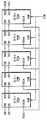
도 2는 캐스케이드된 클록을 갖는 직렬 데이지 체인 캐스케이딩 배열로 구성된 복수의 단일 포트 장치(210a∼e)를 포함하는 예시적인 장치 구성의 블록도이다. 각 장치(210)는 상술한 바와 같이, SI, SO, SCLK 입력 및 CS# 입력을 포함한다. 또한, 각 장치(210)는 클록 출력(SCLKO)을 포함한다. SCLKO는 SCLK 신호 입력을 장치(210)에 출력하는 출력이다.2 is a block diagram of an exemplary device configuration including a plurality of
도 2를 참조하면, 장치들(210)의 SI 및 SO는 상술한 바와 같이, 데이지 체인 캐스케이드 배열로 연결된다. 게다가, 장치들의 SCLK 입력 및 SCLKO는 또한 데이지 체인 캐스케이드 배열로 연결되어, 데이지 체인 캐스케이드에서의 더 앞의 장치(210)의 SCLKO가 데이지 체인 캐스케이드에서의 이후의 장치(210)의 SCLK 입력에 연결되게 된다. 따라서, 예를 들면, 장치(210a)의 SCLKO는 장치(210b)의 SCLK 입력에 연결된다.Referring to FIG. 2, SI and SO of devices 210 are connected in a daisy chain cascade arrangement, as described above. In addition, the SCLK input of the devices and SCLKO are also connected in a daisy chain cascade arrangement so that the SCLKO of the earlier device 210 in the daisy chain cascade is connected to the SCLK input of the subsequent device 210 in the daisy chain cascade do. Thus, for example, the SCLKO of
클록 신호는 데이지 체인 캐스케이드된 장치들을 통해 전파하므로, 지연을 초래할 수 있음에 유의하라. 지연 록트 루프(DLL) 회로와 같은 내부 지연 보상 회로가 이러한 지연을 제거하도록 채용될 수도 있다.Note that clock signals propagate through daisy-chain cascaded devices, which can lead to delays. An internal delay compensation circuit such as a delay locked loop (DLL) circuit may be employed to eliminate this delay.
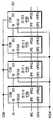
도 3은 직렬 데이지 체인 캐스케이드 배열로 구성된 복수의 이중 포트 장치들(310a∼e)을 포함하는 예시적인 장치 구성의 블록도이다. 각 장치(310)는 상술한 바와 같이, 각 포트에 대해 SI 및 SO, SCLK 입력 및 CS# 입력을 포함한다. 도 3을 참조하면, 장치(310) 상의 제1 포트에 대한 SI는 "SI0"의 라벨로 나타내고, 제2 포트에 대한 SI는 "SI1"의 라벨로 나타낸다. 유사하게, 제1 포트에 대한 SO는 "SO0"의 라벨로 나타내고, 제2 포트에 대해서는 "SO1"의 라벨로 나타낸다. 각 포트에 대한 SI 및 SO는 상술한 바와 같이, 장치들(310) 사이에 접속된다. 따라서, 예를 들면, 장치(310a) 상의 포트 0의 SO가 장치(310b) 상의 포트 0의 SI에 공급된다. 유사하게, 장치(310a) 상의 포트 1의 SO가 장치(310b) 상의 포트 1의 SI에 공급된다.3 is a block diagram of an exemplary device configuration including a plurality of
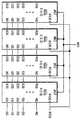
도 4는 여러 가지 인에이블 신호용의 입력 및 출력을 갖는 직렬 데이지 체인 배열로 구성된 복수의 단일 포트 장치를 포함하는 예시적인 장치 구성의 블록도이다. 각 장치(410)는 상술한 바와 같이, SI, SO, CS# 입력, SCLK 입력을 포함한다. 또한, 각 장치(410)는 입력 포트 인에이블(IPE) 입력, 출력 포트 인에이블(OPE) 입력, 입력 포트 인에이블 출력(IPEQ) 및 출력 포트 인에이블 출력(OPEQ)을 포함한다. IPE 입력은 IPE 신호를 장치에 입력하는 데 사용된다. IPE 신호는 장치에 의해 SI를 인에이블시키는 데 사용되어, IPE가 어써트될 때 SI를 통해 장치(410)에 정보가 직렬로 입력될 수 있게 된다. 유사하게, OPE 입력은 장치에 OPE 신호를 입력하는 데 사용된다. OPE 신호는 장치에 의해 SO를 인에이블시키는 데 사용되어, OPE가 어써트될 때 SO를 통해 장치(410)로부터 정보가 직렬로 출력될 수 있게 된다. IPEQ 및 OPEQ는 각각, 장치로부터 IPE 및 OPE를 출력하는 출력들이다. IPEQ 신호는 지연된 IPE 신호이거나, IPE 신호의 어떤 파생물(derivative)일 수도 있다. 유사하게, OPEQ 신호는 지연된 OPE 신호이거나, OPE 신호의 어떤 파생물일 수도 있다. CS# 입력 및 SCLK 입력은 상술한 바와 같이, 장치들(410a∼d)에 CS# 및 SCLK 신호를 각각 분배하는 별개의 링크들에 연결된다.4 is a block diagram of an exemplary device configuration including a plurality of single port devices configured in a serial daisy chain arrangement having input and output for various enable signals. Each device 410 includes SI, SO, CS # input, and SCLK input, as described above. Each device 410 also includes an input port enable (IPE) input, an output port enable (OPE) input, an input port enable output (IPEQ), and an output port enable output (OPEQ). The IPE input is used to input the IPE signal to the device. The IPE signal is used by the device to enable the SI so that information can be serially input to the device 410 via the SI when the IPE is asserted. Similarly, the OPE input is used to input the OPE signal to the device. The OPE signal is used by the device to enable SO so that information can be output serially from the device 410 via the SO when the OPE is asserted. IPEQ and OPEQ are outputs that output IPE and OPE from the device, respectively. The IPEQ signal may be a delayed IPE signal or some derivative of the IPE signal. Similarly, the OPEQ signal may be a delayed OPE signal or some derivative of the OPE signal. The CS # input and the SCLK input are coupled to separate links that distribute the CS # and SCLK signals, respectively, to the
SI 및 SO는 상술한 바와 같이, 데이지 체인 캐스케이드 배열로 하나의 장치로부터 다음의 장치로 연결된다. 또한, 데이지 체인 캐스케이드에서의 더 앞의 장치(410)의 IPEQ 및 OPEQ는 각각, 데이지 체인 캐스케이드에서의 다음의 장치(410)의 IPE 입력 및 OPE 입력에 연결된다. 이러한 배열은 직렬 데이지 체인 캐스케이드 방식으로 하나의 장치(410)로부터 다음의 장치로 IPE 및 OPE 신호가 전송될 수 있게 한다.SI and SO are connected from one device to the next in a daisy chain cascade arrangement, as described above. Also, IPEQ and OPEQ of the earlier device 410 in the daisy chain cascade are each connected to the IPE input and OPE input of the next device 410 in the daisy chain cascade. This arrangement allows IPE and OPE signals to be transmitted from one device 410 to the next in a daisy-chain cascade manner.
도 5는 여러 가지 인에이블 신호용으로 구성된 입력 및 출력을 갖는 직렬 데이지 체인 배열로 구성된 이중 포트 장치(510a∼d)를 포함하는 예시적인 장치 구성의 블록도이다. 각 장치(510)는 상술한 바와 같이, 각 포트에 대해 CS# 입력, SCLK 입력, 및 SI, SO, IPE, OPE, IPEQ 및 OPEQ를 포함한다. 포트 1 및 포트 2에 대한 SI, SO, IPE, OPE, IPEQ 및 OPEQ는 각각, SI1, SO1, IPE1, OPE1, IPEQ1 및 OPEQ1과, SI2, SO2, IPE2, OPE2, IPEQ2 및 OPEQ2로 나타낸다.5 is a block diagram of an exemplary device configuration including a
각 장치(510)에 대한 CS# 입력은 상술한 바와 같이, 단일 링크에 연결되어 모든 장치들(510)을 동시에 선택한다. 유사하게, 각 장치(510)에 대한 SCLK는 상술한 바와 같이, 단일 링크에 연결되어 클록 신호를 모든 장치들(510)에 동시에 분배하도록 구성된다. 또한, 상술한 바와 같이, SI, SO, IPE, OPE, IPEQ 및 OPEQ는, 데이지 체인 캐스케이드에서의 더 앞의 장치의 SO, IPEQ 및 OPEQ가 데이지 체인 캐스케이드에서의 더 뒤의 장치의 SI, IPE 및 OPE에 연결되도록, 장치들 사이에 연결된다. 예를 들면, 장치(510a)의 SO1, SO2, IPEQ1, IPEQ2, OPEQ1, 및 OPEQ2는 각각, 장치(510b)의 SI1, SI2, IPE1, IPE2, OPE1, 및 OPE2에 연결된다.The CS # input to each device 510 is connected to a single link to select all the devices 510 at the same time, as described above. Similarly, the SCLK for each device 510 is configured to be coupled to a single link to simultaneously distribute the clock signal to all of the devices 510, as described above. Also, as described above, SI, SO, IPE, OPE, IPEQ and OPEQ can be used to determine the SI, IPEQ and OPEQ of the earlier devices in the daisy chain cascade, To be connected to the OPE. For example, SO1, SO2, IPEQ1, IPEQ2, OPEQ1, and OPEQ2 of
장치(510a)의 SI, IPE 및 OPE에 입력되는 SI, IPE 및 OPE 신호들은 각각 예컨대, 메모리 제어기(도시 생략)로부터 장치(510a)에 제공된다. 장치(510d)는데이터 및 제어 신호를 장치(510d)의 SO, IPEQ 및 OPEQ 출력들을 통해 메모리 제어기에 되돌려 제공된다.The SI, IPE, and OPE signals that are input to the SI, IPE, and OPE of the
도 6은 직렬 데이지 체인 캐스케이딩 배열로 구성되는 복수의 직렬 입력들(SI0∼SIn) 및 복수의 직렬 출력들(SO0∼SOn)을 갖는 복수의 장치들(610a∼d)을 포함하는 예시적인 장치 구성의 블록도이다. 또한, 각 장치(610)는 상술한 바와 같이, SCLK 입력 및 CS# 입력을 갖는다.Figure 6 shows an exemplary embodiment of a system including a plurality of
각 장치(610)에 대해 채용된 직렬 입력들(SI0∼SIn) 및 직렬 출력들(SO0∼SOn)은 각각, 정보가 직렬 방식으로 장치(610)로 입력되고 장치(610)로부터 출력될 수 있게 한다. 각 입력에는, 특정한 타입의 정보(예컨대, 어드레스, 커맨드, 데이터) 및/또는 신호들(예컨대, 인에이블 신호들)을 장치(610)에 입력하기 위한 특정 역할이 할당될 수 있다. 유사하게, 각 출력에는, 장치(610)로부터의 특정한 타입의 정보 및 신호들을 출력하기 위한 특정 역할이 할당될 수 있다. 예를 들면, 하나 이상의 입력들에, 어드레스 정보를 장치(610)에 입력될 수 있게 하기 위한 역할이 할당될 수도 있다. 유사하게, 예를 들면, 하나 이상의 출력들에, 어드레스 정보를 장치(610)로부터 출력될 수 있게 하기 위한 역할이 할당될 수도 있다.The serial inputs SI0-SnIn and serial outputs SO0-SOn employed for each device 610 are each such that information is input to the device 610 in a serial fashion and output from the device 610 do. Each input may be assigned a specific role for inputting specific types of information (e.g., address, command, data) and / or signals (e.g., enable signals) to the device 610. Similarly, each output may be assigned a specific role for outputting specific types of information and signals from device 610. [ For example, one or more inputs may be assigned a role to enable address information to be input to the device 610. [ Similarly, for example, one or more outputs may be assigned a role to enable address information to be output from the device 610. [
각 장치(610)에 대한 직렬 입력들 및 직렬 출력들의 수는 일반적으로, 어드레스 라인의 수, 커맨드 크기 및 데이터 폭 크기와 같은 특정한 인자들(factors)에 의존한다. 이들 인자는 장치가 특정 시스템 애플리케이션에서 어떻게 사용되는지에 의해 영향을 받을 수 있다. 예를 들면, 소량의 정보를 저장하는 데 사용되는 데이터 저장장치를 필요로 하는 시스템 애플리케이션은, 대량의 정보용의 데이터 저장장치를 필요로 하는 시스템 애플리케이션보다 더 적은 어드레스 및 데이터 라인, 그에 따라 더 적은 입력/출력을 갖는 장치를 채용할 수도 있다.The number of serial inputs and serial outputs for each device 610 generally depends on certain factors such as the number of address lines, command size, and data width size. These factors can be influenced by how the device is used in a particular system application. For example, a system application that requires a data storage device used to store a small amount of information may require fewer address and data lines than a system application that requires a large amount of informational data storage device, An apparatus having an input / output may be employed.
도 7은 직렬 데이지 체인 캐스케이딩 배열로 구성된 단일 장치 및 그 배열로 구성된 복수의 장치에서 실행되는 판독 동작과 관련된 타이밍을 도시하는 타이밍도이다. 도 7을 참조하면, CS#이 모든 장치들을 선택하도록 어써트된다. 판독 동작은 IPE를 어써트하고 SI를 통해 장치로 판독 동작과 관련된 정보를 클록함으로써 시작한다. 예시적으로, 이 정보는 판독 동작이 실행될 것을 나타내는 커맨드(CMD)과, 데이터가 판독되는 메모리 내의 개시 위치를 나타내는 칼럼 어드레스(Col. ADD) 및 로우 어드레스(Row ADD)를 포함한다.7 is a timing diagram illustrating the timing associated with a read operation performed on a single device configured with a serial daisy-chain cascading arrangement and a plurality of devices configured with the array. Referring to FIG. 7, CS # is asserted to select all devices. The read operation begins by asserting the IPE and clocking the information associated with the read operation to the device via SI. Illustratively, this information includes a command (CMD) indicating that a read operation is to be performed, a column address (Col.ADD) and a row address (Row ADD) indicating the start position in the memory where data is read.
시간 "tR"에서, 요구된 데이터가 메모리로부터 판독되어, 장치 내에 포함되는 특수한 내부 데이터 버퍼에 위치한다. tR의 길이는 일반적으로, 메모리를 포함하는 셀의 특성에 의해 결정된다. 시간 tR 후에, OPE가 어써트되어 내부 데이터 버퍼로부터 SO를 통해 데이지 체인 캐스케이드에서의 다음의 장치로의 데이터의 직렬 전송을 인에이블시킨다. 데이터는 SO 출력에서 예시적으로, SCLK 상승 에지에서 내부 버퍼로부터 직렬로 출력된다. 데이지 체인 캐스케이드에서의 장치로부터 출력된 데이터는 예를 들면, IPE 및 OPE와 같은 제어 데이터를 전파하는 것과 관련된 지연을 제어하기 위해 1 클록 사이클만큼 지연된다. 더 이후에 설명하는 바와 같이, 지연 제어는 클록 동기화된 래치를 사용하여 실행된다.At time "tR ", the requested data is read from memory and located in a special internal data buffer included in the device. The length of tR is generally determined by the characteristics of the cell containing the memory. After time tR, the OPE is asserted to enable serial transmission of data from the internal data buffer to the next device in the daisy chain cascade via SO. Data is output serially from the internal buffer at the SCLK rising edge, illustratively at the SO output. Data output from the device in the daisy-chain cascade is delayed by one clock cycle to control the delay associated with propagating control data, such as, for example, IPE and OPE. As described further below, the delay control is performed using a clock synchronized latch.
플래시 코어 구조 실현을 위한 캐스케이드된 메모리 장치들의 동작의 일부 예들이 아래의 표 1에 도시된다. 표 1은 타깃 장치 어드레스(TDA), 가능한 OP(동작) 코드, 그리고 칼럼 어드레스, 로우/뱅크 어드레스 및 입력 데이터의 대응하는 상태들을 리스트한다.
Some examples of the operation of cascaded memory devices for flash core architecture realization are shown in Table 1 below. Table 1 lists the target device address (TDA), possible OP (operation) codes, and corresponding states of the column address, row / bank address, and input data.
[표 1] 커맨드 세트[Table 1] Command set

본 발명의 일부 실시예에서, 도 1∼6에 도시된 시스템 내의 각 장치는 직렬 입력 데이터 내의 타깃 장치 어드레스(tda)로서 사용될 수 있는 고유 장치 식별자를 가질 수 있다. 직렬 입력 데이터를 수신할 때, 플래시 메모리 장치는 직렬 입력 데이터 내의 타깃 장치 어드레스 필드를 파싱하여, 타깃 장치 어드레스를 장치의 고유 장치 식별 번호와 상관시킴으로써 장치가 타깃 장치인지를 판정할 수 있다.
In some embodiments of the invention, each device in the system shown in Figs. 1-6 may have a unique device identifier that can be used as the target device address tda in the serial input data. Upon receiving the serial input data, the flash memory device may determine whether the device is the target device by parsing the target device address field in the serial input data and correlating the target device address with the unique device identification number of the device.
표 2는 도 1∼6과 관련하여 설명한 시스템들을 포함하는 본 발명의 실시예들에 따르는 입력 데이터 스트림의 바람직한 입력 시퀀스를 도시한다. 커맨드들, 어드레스들 및 데이터가 최상위 비트에서 시작하여, 각 메모리 장치의 내외로 직렬로 시프트된다.Table 2 shows the preferred input sequence of the input data stream in accordance with embodiments of the present invention including the systems described with respect to Figures 1-6. Commands, addresses and data are shifted in series into and out of each memory device starting at the most significant bit.
도 4를 참조하면, 장치들(410a∼d)은, 입력 포트 인에이블(IPE)이 HIGH인 동안 직렬 클록(SCLK)의 상승 에지에서 샘플링된 직렬 입력 신호(SIP)로 동작될 수 있다. 커맨드 시퀀스들은 1 바이트 타깃 장치 어드레스("tda") 및 커맨드 코드(표 1에서 "cmd")라고도 교환 가능하게 칭해지는 1 바이트 동작 코드에서 시작한다. 최상위 비트에서의 1 바이트 타깃 장치 어드레스에서 직렬 입력 신호를 시작함으로써, 장치는 수신되는 임의의 부가 입력 데이터를 처리하기 전에 타깃 장치 어드레스 필드를 파싱할 수 있다. 메모리 장치가 타깃 장치가 아니면, 그 장치는 직렬 입력 데이터를 처리하기 전에 다른 장치에 전송할 수 있으며, 그에 따라 부가적인 처리 시간 및 자원을 절약할 수 있다.Referring to FIG. 4, the
[표 2] 바이트 모드에서의 입력 시퀀스[Table 2] Input sequence in byte mode

1 바이트 TDA가 장치로 시프트되고, 1 바이트 cmb 코드가 뒤따른다. 최상위 비트(MSB)는 SIP에서 시작하고, 각 비트는 직렬 클록(SCLK)의 상승 에지에서 래치된다. 커맨드에 따라, 1 바이트 커맨드 코드에는 칼럼 어드레스 바이트, 로우 어드레스 바이트, 뱅크 어드레스 바이트, 데이터 바이트, 및/또는 그 조합이 뒤따를 수 있거나 또는 아무것도 뒤따르지 않을 수도 있다.The 1 byte TDA is shifted to the device, followed by the 1 byte cmb code. The most significant bit (MSB) starts in SIP, and each bit is latched on the rising edge of the serial clock (SCLK). Depending on the command, the 1-byte command code may be followed by column address byte, row address byte, bank address byte, data byte, and / or combination thereof, or nothing at all.
도 8은 직렬 데이지 체인 캐스케이드 배열로 구성된 장치들 사이에서 전송되는 정보와 관련된 타이밍을 도시하는 타이밍도이다. 상기와 같이, CS#은 장치들을 선택하기 위해 어써트된다. IPE를 어써트하고 SCLK의 연속적인 상승 에지에서 장치에 데이터를 클록함으로써, 데이지 체인 캐스케이드에서의 제1 장치에 정보가 입력된다. IPE는 1 사이클 미만에서 제1 장치를 통해 제2 장치로 전파된다. 이것은, 정보가 제1 장치 내에 클록된 후의 1 사이클에서, 제1 장치의 SO로부터 제2 장치의 SI로 정보가 클록될 수 있게 한다. 이것은 데이지 체인 캐스케이드 내의 연속하는 장치들에 대해 반복된다. 따라서, 예를 들면, 정보는 제1 장치에서의 데이터의 래치 포인트로부터 SCLK의 제3 상승 에지에서 직렬 데이지 체인 캐스케이드 내의 제3 장치에 입력된다. 제어 신호들 IPE 및 OPE는 데이지 체인 캐스케이드 내의 다음의 장치에서 이들 신호에 대한 적절한 설정 시간을 보증하기 위해 SCLK의 상승 에지와 동기화된다.8 is a timing diagram illustrating the timing associated with information transmitted between devices configured with a serial daisy-chain cascade arrangement. As above, CS # is asserted to select devices. Information is input to the first device in the daisy chain cascade by asserting the IPE and clocking the data to the device at successive rising edges of SCLK. The IPE is propagated from the first device to the second device in less than one cycle. This allows information to be clocked from the SO of the first device to the SI of the second device in one cycle after the information is clocked in the first device. This is repeated for successive devices in a daisy chain cascade. Thus, for example, information is input to the third device in the serial daisy-chain cascade at the third rising edge of SCLK from the latch point of the data at the first device. The control signals IPE and OPE are synchronized with the rising edge of SCLK to ensure proper setup time for these signals in the next device in the daisy chain cascade.
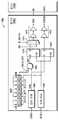
도 9는 단일 포트의 장치용의 예시적인 직렬 출력 제어 로직(900)의 블록도이다. 로직(900)은 IPE용 입력 버퍼(902), SI(SIP)용 입력 버퍼(904), OPE용 입력 버퍼(906), 입력 래치 제어(908), 직렬-병렬 레지스터(910), 출력 래치 제어(912), 데이터 레지스터(914), 어드레스 레지스터(916), 커맨드 해석기(918), 셀렉터(920), 페이지 버퍼(924), 논리 OR 게이트(926), 출력 버퍼(928), 셀렉터(930) 및 메모리(950)를 포함한다.9 is a block diagram of an exemplary serial
입력 버퍼(902)는 버퍼(902)의 입력에서 장치에 공급되는 IPE 신호의 상태를 버퍼링하도록 구성되는 통상적인 저 전압 트랜지스터-트랜지스터 로직(LVTTL) 버퍼이다. 버퍼(902)의 출력은, IPE 신호의 상태를 래치하고 IPE 신호의 래치된 상태를 입력 버퍼(904) 및 셀렉터(920)에 제공하는 입력 래치 제어(908)에 공급된다. 입력 버퍼(904)는 SI 입력을 통해 장치에 공급되는 정보를 버퍼링하도록 구성되는 LVTTL 버퍼이다. 입력 버퍼(904)는 입력 래치 제어(908)의 출력에 의해 인에이블된다. 인에이블될 때, SI 입력에 제공되는 정보는 버퍼(908)에 의해 직렬-병렬 레지스터(910) 및 셀렉터(930)의 입력에 공급된다. 입력 버퍼(904)는, 입력 래치 제어(908)로부터 공급되는 IPE 신호의 래치된 상태가, IPE 신호가 어써트된 것을 나타낼 때 인에이블된다. 직렬-병렬 레지스터(910)에 공급되는 정보는 레지스터(910)에 의해 직렬 형태에서 병렬 형태로 변환된다. 직렬-병렬 레지스터(910)의 출력들은 데이터 레지스터(914), 어드레스 레지스터(916) 및 커맨드 해석기(918)에 공급된다.The
데이터 레지스터(914) 및 어드레스 레지스터(916)는 SI를 통해 장치에 공급되는 데이터 및 어드레스 정보를 각각 유지한다. 커맨드 해석기(918)는 SI를 통해 장치에 입력되는 커맨드를 해석하도록 구성된다. 이들 커맨드는 장치의 동작을 더욱 제어하기 위해 사용된다. 예를 들면, "기록 메모리" 커맨드는, 장치가 데이터 레지스터(914)에 포함된 데이터를, 어드레스 레지스터(916)에 의해 특정되는 어드레스에서 장치에 포함되는 메모리(950)에 기록하게 하는 데 사용될 수 있다.Data register 914 and address register 916 maintain data and address information, respectively, supplied to the device via SI. The
입력 버퍼(906)는 장치의 OPE 입력에 공급되는 OPE 신호를 버퍼링하도록 구성되는 LVTTL 버퍼이다. 버퍼(906)의 출력은 OPE 신호의 상태를 래치하는 출력 래치 제어(912)에 전송된다. 출력 래치 제어는 래치된 OPE 신호 상태를 OR 게이트(926)에 출력한다. OR 게이트(926)는, 그 출력이 출력 버퍼(928)의 출력을 인에이블/디스에이블시키는 데 사용되는 통상적인 논리 OR 게이트이다.The
셀렉터(920)는 신호 DAISY_CHAIN에 의해 선택되는 바와 같은 2개의 입력 중 하나를 출력하는 통상적인 2-투(to)-1 멀티플렉서이다. 상기 논의된 바와 같이, 이들 입력 중 하나는 입력 래치 제어(908)로부터의 IPE의 래치된 상태이다. 다른 입력은 논리 저 조건으로 설정된다. 신호 DAISY_CHAIN은, 장치가 직렬 데이지 체인 캐스케이드 배열 내의 하나 이상의 다른 장치들에 연결되는지를 나타낸다. 예시적으로, 이 신호는, 장치가 직렬 데이지 체인 캐스케이드 배열 내의 하나 이상의 장치들에 연결되면 어써트된다. DAISY_CHAIN 신호를 어써트하면 셀렉터(920)에 공급되는 IPE 신호의 래치된 상태가 셀렉터(920)로부터 출력된다. DAISY_CHAIN이 어써트되지 않을 때, 셀렉터(920)로의 논리 저 조건 입력이 셀렉터(920)로부터 출력된다.The
페이지 버퍼(924)는 메모리(950)로부터 판독되는 정보를 유지하도록 구성되는 통상적인 데이터 버퍼이다. 셀렉터(930)는 신호 ID_MATCH에 의해 선택된 것으로서 2개의 입력 중 하나를 출력하는 통상적인 2-투-1 멀티플렉서이다. 셀렉터(930)로의 하나의 입력은 페이지 버퍼(924)의 출력으로부터 공급되고, 다른 입력은 SI 입력 버퍼(904)의 출력으로부터 공급된다. 셀렉터(930)의 출력은 출력 버퍼(928)에 공급된다. 신호 ID_MATCH는, SI를 통해 장치에 전송되는 특정 커맨드가 장치에 어드레스되는지를 나타낸다. 커맨드가 장치에 어드레스되면, ID_MATCH가 어써트되어, 페이지 버퍼(924)로부터의 출력이 셀렉터(930)로부터 출력되게 한다. ID_MATCH가 어써트되지 않으면, SI 버퍼(904)로부터의 출력(즉, 장치로 입력되는 SI 신호의 상태)이 셀렉터(930)로부터 출력된다.The
메모리(950)는 데이터를 유지하도록 구성되는 통상적인 메모리이다. 메모리(950)는 SI를 통해 장치에 입력되는 어드레스를 사용하여 어드레스 가능한 정적 RAM(SRAM), 동적 RAM(DRAM) 또는 플래시 메모리 셀과 같은 셀들을 포함하는 랜덤 액세스 메모리(RAM)일 수 있다.
동작적으로는, 어써트된 IPE 신호가 입력 버퍼(902)에 의해 버퍼링되어, IPE의 어써트된 상태를 래치하는 입력 래치 제어(908)에 전송된다. 이 래치된 상태는 셀렉터(920)에 그리고 입력 버퍼(904) 공급되어, 이 버퍼(904)를 인에이블시킨다. 입력 버퍼(904)에 입력되는 커맨드, 어드레스 및 데이터 정보는 그 후, 정보를 직렬 형태에서 병렬 형태로 변환시키고 커맨드, 어드레스 및 데이터 정보를 각각 커맨드 해석기(918), 어드레스 레지스터(916) 및 데이터 레지스터(914)에 공급하는 직렬-병렬 레지스터(910)에 공급된다. 버퍼(904)의 출력은 또한 셀렉터(930)에 공급된다. ID_MATCH가 어써트되지 않으면, 버퍼(904)의 출력은 출력 버퍼(928)의 입력에 공급되는 셀렉터(930)의 출력에 존재한다. DAISY_CHAIN이 어써트되면, IPE의 래치된 상태는 셀렉터(920)의 출력에 존재하고 OR 게이트(926)의 제1 입력에 공급된다. OR 게이트(926)는 IPE의 상태를 출력 버퍼(928)에 전달하여 출력 버퍼(928)를 인에이블시킨다. 이것은 차례로, SI 입력으로 입력되는 정보가 SO에서 장치로부터 출력될 수 있게 한다.Operationally, the asserted IPE signal is buffered by the
페이지 버퍼(924)로부터의 데이터는 OPE 및 ID_MATCH를 어써트함으로써 장치로부터 출력된다. 구체적으로는, OPE의 어써트된 상태가 입력 버퍼(906)에 공급되고, 차례로 그 상태를 출력 래치 제어(912)에 공급하여 그 상태를 래치한다. 래치된 어써트된 상태는, 출력 버퍼(928)를 인에이블시키도록 신호를 출력하는 OR 게이트(926)의 제2 입력에 공급된다. ID_MATCH를 어써트하면 페이지 버퍼(924)의 출력이 셀렉터(930)의 출력에 존재하게 할 수 있다. 셀렉터(930)의 출력은 장치의 SO 출력에서 장치로부터 데이터를 출력하는 인에이블된 출력 버퍼(928)에 공급된다.Data from
DAISY_CHAIN이 어써트되지 않으면, 출력 버퍼(928)가 OPE에 의해 인에이블되기만 한다. 이것은 장치가 비데이지(non-daisy) 체인 직렬 캐스케이드 구성에 사용될 수 있게 한다.If DAISY_CHAIN is not asserted, the
도 10은 이중 포트의 장치용의 예시적인 직렬 출력 제어 로직(1000)의 블록도이다. 각 포트에 대해, 직렬 출력 제어 로직(1000)은 IPE 입력 버퍼(1002), SI 입력 버퍼(1004), OPE 입력 버퍼(1006), 입력 래치 제어(1008), 직렬-병렬 레지스터(1010), 출력 래치 제어(1012), 데이터 레지스터(1014), 어드레스 레지스터(1016), 커맨드 해석기(1018), 셀렉터(1020), 페이지 버퍼(1024), 논리 OR 게이트(1026), 출력 버퍼(1028) 및 셀렉터(1030)를 포함하며, 이들은 각각, 상술한 IPE 입력 버퍼(902), SIP 입력 버퍼(904), OPE 입력 버퍼(906), 입력 래치 제어(908), 직렬-병렬 레지스터(910), 출력 래치 제어(912), 데이터 레지스터(914), 어드레스 레지스터(916), 커맨드 해석기(918), 셀렉터(920), 페이지 버퍼(924), 논리 OR 게이트(926), 출력 버퍼(928) 및 셀렉터(930)와 동일하다.10 is a block diagram of an exemplary serial
도 11은 여기에서 설명하는 기술과 함께 사용될 수 있는 직렬 출력 제어 로직(1100)의 다른 실시예의 상세한 블록도이다. 로직(1100)은 SI 입력 버퍼(1104), IPE 입력 버퍼(1106), OPE 입력 버퍼(1108), SCLK 입력 버퍼(1110), 논리 AND 게이트들(1112 및 1114), 래치들(1116, 1118, 1120 및 1122), 셀렉터들(1124 및 1130), 논리 OR 게이트(1126) 및 SO 출력 버퍼(1128)를 포함한다. 버퍼들(1104, 1106, 1108 및 1110)은 각각, 장치에 입력되는 SI, IPE, OPE 및 SCLK 신호를 버퍼링하도록 구성되는 통상적인 LVTTL 버퍼들이다.11 is a detailed block diagram of another embodiment of the serial
AND 게이트(1112)는, IPE가 어써트될 때 SI로 입력되는 정보를 래치(1116)에 출력하도록 구성된다. 래치(1116)는 클록 신호(SCLK)가 버퍼(1110)에 의해 제공될 때 정보를 래치하도록 구성된다. DATA_OUT은 장치에 포함되는 메모리(도시 생략)로부터 판독되는 데이터의 상태를 나타낸다. AND 게이트(1114)는 OPE가 어써트될 때 DATA_OUT의 상태를 출력하도록 구성된다. AND 게이트(1114)의 출력은, 클록 신호가 버퍼(1110)에 의해 제공될 때 DATA_OUT의 상태를 래치하도록 구성되는 래치(1118)에 공급된다. 버퍼(1106)는 장치에 공급되는 IPE 신호를 버퍼링하도록 구성된다. 버퍼(1106)의 출력은 래치(1120)에 의해 래치된다. 유사하게, 버퍼(1108)는 장치에 공급되는 OPE 신호를 버퍼링하도록 구성된다. 래치(1122)는 버퍼(1108)에 의한 출력으로서 OPE의 상태를 래치하도록 구성된다. 셀렉터들(1124 및 1130)은 2개의 입력을 각각 포함하는 통상적인 2-투-1 멀티플렉서들이다. 셀렉터(1124)에 대한 입력들은 상술한 ID_MATCH 신호에 의해 셀렉터(1124)로부터의 출력을 위해 선택된다. 하나의 입력은 래치(1118)에 의해 유지되는 것으로서 DATA_OUT의 래치된 상태와 함께 공급된다. 이 입력은, ID_MATCH가 어써트될 때 셀렉터(1124)로부터의 출력을 위해 선택된다. 다른 입력은 래치(1116)에 의해 유지되는 것으로서 SI의 래치된 상태와 함께 공급된다. 이 입력은 ID_MATCH가 어써트되지 않을 때 셀렉터(1124)로부터의 출력을 위해 선택된다.The AND
셀렉터(1130)에 대한 입력들은 상술한 DAISY_CHAIN 신호에 의한 셀렉터(1130)로부터의 출력을 위해 선택된다. 셀렉터(1130)로의 하나의 입력은 래치(1120)에 의해 유지되는 것으로서 IPE의 래치된 상태와 함께 공급되고, 다른 입력은 논리 제로(0)로 구속된다. IPE의 래치된 상태는 DAISY_CHAIN이 어써트될 때 셀렉터(1130)로부터의 출력을 위해 선택된다. 유사하게, DAISY_CHAIN이 어써트되지 않을 때, 논리 제로가 셀렉터(1130)로부터의 출력을 위해 선택된다.The inputs to the
OR 게이트(1126)는 인에이블/디스에이블 신호를 출력 버퍼(1128)에 제공하도록 구성되는 통상적인 논리 OR 게이트이다. OR 게이트(1126)에는 셀렉터(1130)의 출력과 함께 래치(1122)에 의해 유지되는 것으로서 OPE의 래치된 상태가 공급된다. 이들 출력 중 어느 하나는 인에이블 신호를 버퍼(1128)에 제공하여 버퍼의 출력을 인에이블시키는 데 사용될 수 있다. 버퍼(1128)는 출력 신호 SO를 버퍼링하는 통상적인 버퍼이다. 상기 논의된 바와 같이, 버퍼(1128)는 OR 게이트(1126)의 출력에 의해 인에이블/디스에이블된다.OR
동작적으로는, IPE가 어써트될 때, SI를 통해 장치에 입력되는 정보가 래치(1116)에 공급된다. 래치(1116)는 이 정보를, IPE가 어써트된 후 예시적으로 SCLK의 제1 상향 전이 시에 래치한다. 유사하게, 래치(1120)는 이 SCLK 전이 시에 IPE의 상태를 래치한다. ID_MATCH가 어써트되지 않는다고 가정하면, 래치(1116)의 출력은 셀렉터(1124)를 통해 버퍼(1128)에 공급된다. 유사하게, 어써트된 IPE는 버퍼(1106)로부터, 그것이 또한 예시적으로 SCLK의 제1 상향 전이에 의해 래치되는 래치(1120)에 전송된다. DAISY_CHAIN이 어써트된다고 가정하면, IPE의 래치된 상태가 셀렉터(1130)의 출력에 제공되고 OR 게이트(1126)에 전송되어 인에이블 신호를 버퍼(1128)에 제공한다. SI의 래치된 상태는 그 후 출력 SO로서 버퍼(1128)를 통해 장치로부터 전송된다.Operationally, when IPE is asserted, information input to the device via SI is provided to latch 1116.
DAISY_CHAIN이 어써트되지 않을 때, 셀렉터(1130)로 입력되는 논리 제로가 선택되어 셀렉터(1130)로부터 논리 제로를 출력한다. 이것은 인에이블한 버퍼(1128)로부의 IPE를 효과적으로 디스에이블시킨다.When DAISY_CHAIN is not asserted, a logic zero input to the
예시적으로는, OPE가 어써트된 후 SCLK의 다음의 상향 전이 시에, OPE의 어써트된 상태가 래치(1122)에서 래치되고 DATA_OUT의 상태가 래치(1118)에서 래치된다. ID_MATCH가 어써트된다고 가정하면, DATA_OUT의 래치된 상태가 셀렉터(1124)에 의해 선택되어 버퍼(1128)의 입력에 적용된다. 동시에, 래치(1122)로부터의 OPE의 래치된 어써트된 상태가 OR 게이트(1126)를 통과하여 버퍼(1128)를 인에이블시켜, DATA_OUT의 래치된 상태가 출력 SO로서 장치로부터 출력되게 한다.Illustratively, at the next up transition of SCLK after OPE is asserted, the asserted state of OPE is latched in latch 1122 and the state of DATA_OUT is latched in
도 12는 직렬 데이지 체인 캐스케이딩 배열로 구성되고 예시적인 직렬 출력 제어 로직을 포함하는 장치들의 예시적인 구성의 블록도이다. 그러한 배열은, 상술한 바와 같이, 데이지 체인 캐스케이드 내의 더 앞의 장치의 출력들이 데이지 체인 캐스케이드 내의 다음의 장치의 입력들에 연결되도록 구성되는 3개의 장치들(1210)을 포함한다. 하나의 장치로부터 다음의 장치로의 정보 및 데이터의 전송은 아래의 도 13을 참조하여 설명한다.FIG. 12 is a block diagram of an exemplary configuration of devices configured with a serial daisy-chain cascading arrangement and including exemplary serial output control logic. Such an arrangement includes three devices 1210 that are configured to connect the outputs of the earlier devices in the daisy chain cascade to the inputs of the next device in the daisy chain cascade, as described above. The transfer of information and data from one apparatus to the next apparatus will be described below with reference to FIG.
도 13은 도 12에 도시된 장치들의 입력 및 출력과 관련된 타이밍을 도시하는 예시적인 타이밍도이다. 구체적으로는, 도 13은 각 장치(1210)의 SI 입력에서의 정보 입력을 장치(1210)의 SO 출력에 전달하는 것에 대해 각 장치 내의 직렬 출력 제어 로직(100)의 동작을 도시한다.13 is an exemplary timing diagram illustrating the timing associated with the input and output of the devices shown in Fig. Specifically, FIG. 13 illustrates the operation of the serial output control logic 100 within each device for transferring the information input at the SI input of each device 1210 to the SO output of the device 1210.
도 11, 12 및 13을 참조하면, DAISY_CHAIN이 어써트된다고 가정한다. IPE가 장치(1210a)에서 어써트될 때, 장치의 SI 입력에서의 정보가 장치의 직렬 출력 제어 로직(1100)을 통해 상술한 바와 같이, 장치(1210a)의 SO 출력에 전달된다. 구체적으로는, 데이터는, IPE가 어써트된 후 예시적으로 SCLK의 각 상승 에지에서 장치(1210a)에 클록된다. IPE의 상태 및 정보는 상술한 바와 같이, 로직(1100)을 통해 전파하고, 장치의 SO 및 IPEQ 출력에서 각각, 장치(1210a)를 빠져나간다. 이들 출력은 각각, 도면에서 S1 및 P1로서 나타난다. 이들 출력은 장치(1210b)의 SI 및 IPE 입력에 공급되어, 상술한 바와 같이, 장치(1210b)의 직렬 출력 제어 로직(1100)을 통과하여, 장치의 SO 및 IPEQ 출력들에서 1 클록 사이클 이후에 장치(1210b)로부터 출력된다. 이들 출력은 도면에서 각각, S2 및 P2로 나타난다. 유사하게, 장치(1210b)의 SO 및 IPEQ 출력은 각각, 장치(1210c)의 SI 및 IPE 입력에 공급되어, 장치(1210c)의 직렬 출력 제어 로직(1100)을 통과하여, 장치의 SO 및 IPEQ 출력들에서 1 클록 사이클 이후에 장치(1210c)로부터 출력된다. 이들 출력은 도면에서 각각, S3 및 P3으로 나타난다.Referring to Figs. 11, 12 and 13, it is assumed that DAISY_CHAIN is asserted. When the IPE is asserted at the device 1210a, the information at the SI input of the device is passed to the SO output of the device 1210a, as described above, via the serial
상술한 데이지 체인 캐스케이드 배열에서, SDR 동작을 위한 데이지 체인 캐스케이드 내의 신호들의 출력 지연은 아래의 식을 사용하여 판정될 수 있다.In the daisy chain cascade arrangement described above, the output delay of the signals in the daisy chain cascade for SDR operation can be determined using the following equation.
출력_지연 = N * 클록_사이클_시간Output_delay = N * Clock_cycle_time
여기에서, "출력_지연"은 데이터의 출력 지연이고,Here, "output_delay" is the output delay of the data,
"N"은 데이지 체인 캐스케이드 배열 내의 장치들의 수이며,"N" is the number of devices in the daisy chain cascade arrangement,
"클록_사이클_시간"은 클록(예컨대, SCLK)이 동작하는 클록 사이클 시간이다.Is a clock cycle time at which a clock (e.g., SCLK) operates.
예를 들어, 도 12에 도시된 데이지 체인 캐스케이드에 대한 클록_사이클_시간이 10 나노초라고 가정한다. 장치(1210c)의 SO에서의 데이터에 대한 총 출력 지연은 3*10 나노초 즉, 30 나노초이다.For example, assume that the clock_cycle_time for the daisy chain cascade shown in FIG. 12 is 10 nanoseconds. The total output delay for the data at the SO of device 1210c is 3 * 10 nanoseconds, or 30 nanoseconds.
DDR 동작의 경우에, 출력 지연은 아래와 같이 판정될 수 있다.In the case of DDR operation, the output delay can be determined as follows.
출력_지연 = N * (클록_사이클_시간/2)Output_Delay = N * (Clock_Cycle_Hours / 2)
DDR 동작에서, 클록의 양 에지들은 입력 데이터의 래치 포인트 및 출력 데이터의 변화 포인트로서 작용할 수 있다. 따라서, 총 지연은 SDR 동작에 대한 지연의 1/2이다.In DDR operation, both edges of the clock can act as a latch point of the input data and a changing point of the output data. Thus, the total delay is one-half of the delay for SDR operation.
상기 설명에서, 장치(1210)로 입력되는 정보는 SDR 동작에 대해서는 1 클록 사이클 후에, 그리고 DDR 동작에 대해서는 1½ 사이클 후에 출력된다. 이러한 지연은 출력 버퍼(1128)를 활성화시키는 데 필요한 시간에 적응하도록 도입된다.In the above description, the information input to the device 1210 is output after 1 clock cycle for the SDR operation and after 1½ cycles for the DDR operation. This delay is introduced to adapt to the time required to activate the
도 14는 데이지 체인 캐스케이드 내의 제1 장치(1450a)의 메모리에 포함된 데이터를 데이지 체인 캐스케이드 내의 제2 장치(1450b)로 전송하는 데 사용될 수 있는 로직(1400)의 블록도이다. 로직(1400)은 데이터 출력 레지스터(1402), OPE 입력 버퍼(1404), SCLK 입력 버퍼(1406), AND 게이트(1048), 데이터 출력 래치(1410), OPE 상태 래치(1412), 셀렉터(1414), SO 출력 버퍼(1416) 및 OPEQ 출력 버퍼(1418)를 포함한다.14 is a block diagram of
데이터 출력 레지스터(1402)는 장치(1450)에 포함되는 메모리로부터 판독되는 데이터를 저장하도록 구성된 통상적인 레지스터이다. 그 레지스터(1402)는 예시적으로는 메모리로부터 병렬로 데이터를 로드하고 그 데이터를 게이트(1408)의 입력에 직렬로 전송하는 병렬-직렬 데이터 레지스터이다. SCLK는 레지스터(1402)에 의해 데이터를 게이트(1408)에 전송하는 데 사용되는 클록을 제공한다. 도시된 바와 같이, 데이터 레지스터(1402)는 비트들(D0 내지 D7)을 포함하는 1 바이트의 데이터를 유지하도록 구성되며, 여기에서 D0은 바이트의 최하위 비트(LSB)이고 비트 D7은 바이트의 최상위 비트(MSB)이다. 레지스터(1402)는 메모리로부터의 바이트 폭의 데이터와 병렬로 로드된다. 데이터는 그 후 레지스터로부터 시프트되어, MSB에서 시작하여 게이트(1408)의 입력에 한 비트씩 직렬로 공급된다.
버퍼들(1404 및 1406)은 각각, 입력 신호들(OPE 및 SCLK)을 버퍼링하는 데 사용되는 통상적인 LVTTL 버퍼들이다. OPE 신호는 버퍼(1404)의 출력(OPEI)으로부터 게이트(1408)에 전송된다. SCLK 신호는 버퍼(1406)의 출력으로부터 데이터 출력 레지스터(1402) 및 래치들(1410 및 1412)에 출력되어 클록을 이들 구성요소들에 제공한다.
게이트(1408)는 OPE가 어써트될 때 데이터 출력 레지스터(1402)의 출력(DATA_OUT)을 래치(1410)에 전송하도록 구성되는 통상적인 논리 AND 게이트이다. 게이트(1408)의 출력은 "DBIT"로서 지정된다. 래치들(1410 및 1412)은 각각, DBIT 및 OPE 신호의 상태를 래치하도록 구성되는 통상적인 래치들이다. 셀렉터(1414)는 신호 ID_MATCH에 의해 제어되는 통상적인 2 입력 2-투-1 멀티플렉서이다. 데이터 입력 중 하나는 DBIT의 래치된 상태와 함께 공급된다. 이 상태는, ID_MATCH가 어써트될 때 셀렉터(1414)로부터 출력된다. 다른 입력은 그 SI를 통해 장치(1450a)에 입력되는 직렬 정보(SI0)과 함께 공급된다. 이 정보는, ID_MATCH가 어써트되지 않을 때 셀렉터(1414)에 의해 출력된다.
버퍼들(1416 및 1418)은 각각, 셀렉터(1414) 및 래치(1416)의 출력을 버퍼링하도록 구성되는 통상적인 버퍼들이다. 버퍼(1416)의 출력은 SO(SO0)로서 장치(1450a)를 빠져나가고, 버퍼(1418)의 출력은 OPEQ(OPEQ0)로서 장치(1450a)를 빠져나간다.
도 15는 로직(1400)을 사용하여 장치(1450a)에 포함되는 메모리로부터 장치(1450b)로의 바이트 폭의 데이터를 전송하는 것과 관련된 타이밍을 도시하는 타이밍도이다. 도 14 및 도 15를 참조하면, OPEI는, OPE가 입력 버퍼(1404)에서 장치(1450a)에 공급된 후 짧게 어써트된다. OPEI는 게이트(1408)에 공급되어 데이터 출력 레지스터(1402)의 D7에 존재하는 데이터가 SCLK의 다음의 상승 에지에서 래치(1410)에서 래치될 수 있게 한다. 또한, 이 SCLK의 다음의 상승 에지가 데이터를 데이터 출력 레지스터(1402)에서 우측으로 시프트되게 하여, D6 내의 데이터가 D7로 시프트되고, D5 내의 데이터가 D6으로 시프트되며, 등등이다. 래치(1410)의 출력은 셀렉터(1414)에 제공되어, ID_MATCH가 어써트된다고 가정하면, 데이터의 래치된 상태를 버퍼(1416)에 출력한다. 버퍼(1416)는 이 래치된 상태를 장치(1450a)로부터, 데이지 체인 캐스케이드의 다음의 장치(1450b)의 SI 입력(SI1)에 공급되는 SO0으로서 출력한다. 한편, OPE가 어써트된 후 제1 클록의 상승 에지에서도 또한, OPE의 상태가 래치(1412)에서 래치된다. 래치(1412)의 출력은 버퍼(1418)에 전송되어, OPE의 래치된 상태를 장치(1450a)로부터 데이지 체인 캐스케이드의 다음의 장치(1450b)의 OPE 입력(OPE1)에 공급되는 OPEQ(OPEQ0)로서 출력한다. 이 프로세스는 비트들(D6 내지 D0)에 대해 반복된다.Figure 15 is a timing diagram illustrating the timing associated with transferring byte-wide data from the memory included in
본 발명은 바람직한 실시예를 참조하여 특히 도시 및 설명하였지만, 당업자에게는 첨부하는 청구의 범위에 의해 한정되는 발명의 범위를 벗어남 없이 형태 및 상세내용의 여러 가지 변형이 행해질 수 있다는 것을 이해할 것이다.While the invention has been particularly shown and described with reference to a preferred embodiment, it will be understood by those skilled in the art that various changes in form and details may be made therein without departing from the scope of the invention as defined by the appended claims.
Claims (29)
Translated fromKorean상기 제1 메모리 장치는,
(a) 메모리,
(b) 상기 메모리 내의 메모리 위치에 관련된 어드레스 정보를 수신하는 제1 입력,
(c) 상기 어드레스 정보를 수신하기 위하여 상기 제1 입력을 인에이블 시키는데 사용되는 제1 입력 인에이블 신호를 수신하는 제1 제어 입력,
(d) 지속 시간(duration of time) 동안 제1 로직 레벨로 설정된 제1 출력 인에이블 신호를 수신하는 제 2 제어 입력,
(e) 상기 지속 시간 동안 상기 제1 로직 레벨에 있는 상기 제1 출력 인에이블 신호에 응답하여 상기 메모리 내의 상기 메모리 위치에 포함된 제1 출력 데이터를 제공하는 제1 출력,
(f) 상기 제1 입력 인에이블 신호에 응답하여 제2 입력 인에이블 신호를 제공하는 제1 제어 출력,
(g) 상기 제1 출력 인에이블 신호에 응답하여 제2 출력 인에이블 신호를 제공하는 제2 제어 출력 - 상기 제2 출력 인에이블 신호는 상기 지속 시간 동안 상기 제1 로직 레벨에 있음 - ,
을 포함하고,
상기 제2 메모리 장치는,
(a) 상기 제1 메모리 장치로부터 상기 제2 입력 인에이블 신호를 수신하는 제1 제어 입력,
(b) 수신된 상기 제2 입력 인에이블 신호에 응답하여 상기 제1 메모리 장치로부터 제공된 상기 제1 출력 데이터를 수신하는 제1 입력,
(c) 상기 제1 메모리 장치로부터 상기 제2 출력 인에이블 신호를 수신하는 제2 제어 입력,
(d) 상기 지속 시간 동안 상기 제1 로직 레벨에 있는 수신된 상기 제2 출력 인에이블 신호에 응답하여 후속 장치(subsequent device)로 제2 출력 데이터를 출력하도록 구성되는 제1 출력,
을 포함하며,
상기 제2 출력 데이터는 상기 제2 메모리 장치의 상기 제1 입력에 의해 수신된 상기 제1 출력 데이터 및 상기 제2 메모리 장치에 의하여 제공된 데이터 중 어느 하나인, 데이지 체인 캐스케이드 배열로 구성된 복수의 장치를 갖는 장치.An apparatus having a plurality of devices configured in a daisy chain cascade arrangement comprising a first memory device and a second memory device,
Wherein the first memory device comprises:
(a) memory,
(b) a first input for receiving address information related to a memory location in the memory,
(c) a first control input for receiving a first input enable signal used to enable the first input to receive the address information,
(d) a second control input for receiving a first output enable signal set to a first logic level during a duration of time,
(e) a first output for providing first output data contained in the memory location in the memory in response to the first output enable signal at the first logic level for the duration,
(f) a first control output responsive to the first input enable signal to provide a second input enable signal,
(g) a second control output providing a second output enable signal in response to the first output enable signal, the second output enable signal being at the first logic level during the duration,
/ RTI >
The second memory device comprising:
(a) a first control input for receiving the second input enable signal from the first memory device,
(b) a first input for receiving the first output data provided from the first memory device in response to the received second input enable signal,
(c) a second control input for receiving the second output enable signal from the first memory device,
(d) a first output configured to output second output data to a subsequent device in response to the received second output enable signal at the first logic level during the duration,
/ RTI >
Wherein the second output data is any one of the first output data received by the first input of the second memory device and the data provided by the second memory device, / RTI >
상기 제1 출력 데이터는 상기 제1 메모리 장치의 상기 제1 출력으로부터 상기 제2 메모리 장치의 상기 제1 입력으로 전송된 데이터를 포함하는, 데이지 체인 캐스케이드 배열로 구성된 복수의 장치를 갖는 장치.The method according to claim 1,
Wherein the first output data comprises data transmitted from the first output of the first memory device to the first input of the second memory device.
상기 제1 메모리 장치 및 상기 제2 메모리 장치 각각은 클록 신호를 수신하는 제3 제어 입력을 포함하는, 데이지 체인 캐스케이드 배열로 구성된 복수의 장치를 갖는 장치.The method according to claim 1,
Wherein the first memory device and the second memory device each comprise a third control input for receiving a clock signal.
상기 제1 메모리 장치는, 수신된 상기 클록 신호에 따라 상기 제1 메모리 장치의 상기 메모리에서 상기 제1 메모리 장치의 상기 제1 출력으로 판독 데이터를 전송하도록 구성되는 데이터 전송로(data transfer path)를 포함하며, 상기 제1 출력 데이터는 상기 판독 데이터에 상응하는, 데이지 체인 캐스케이드 배열로 구성된 복수의 장치를 갖는 장치.The method of claim 3,
The first memory device having a data transfer path configured to transfer read data from the memory of the first memory device to the first output of the first memory device in accordance with the received clock signal, And wherein the first output data comprises a plurality of devices in a daisy chain cascade arrangement corresponding to the read data.
상기 제2 메모리 장치는, 수신된 상기 클록 신호에 따라 상기 제2 메모리 장치의 상기 제1 입력에 의하여 수신된 상기 제1 출력 데이터를 상기 제2 메모리 장치의 상기 제1 출력으로 전송하도록 구성되는 데이터 전송로(data transfer path)를 포함하는, 데이지 체인 캐스케이드 배열로 구성된 복수의 장치를 갖는 장치.The method of claim 3,
Wherein the second memory device is configured to receive data that is configured to transfer the first output data received by the first input of the second memory device to the first output of the second memory device in accordance with the received clock signal An apparatus having a plurality of devices configured in a daisy chain cascade arrangement, the device including a data transfer path.
상기 제1 메모리 장치는, 상기 클록 신호를 상기 제1 메모리 장치에서 상기 제2 메모리 장치로 전송하는 상기 제2 메모리 장치의 제3 제어 입력에 연결되는, 제3 제어 출력을 갖는, 데이지 체인 캐스케이드 배열로 구성된 복수의 장치를 갖는 장치.The method of claim 5,
The first memory device having a third control output coupled to a third control input of the second memory device for transferring the clock signal from the first memory device to the second memory device, the daisy chain cascade arrangement ≪ / RTI >
상기 후속 장치는 제3 메모리 장치 및 메모리 제어기 중 어느 하나를 포함하는, 데이지 체인 캐스케이드 배열로 구성된 복수의 장치를 갖는 장치.The method according to claim 1,
Wherein the subsequent device comprises a third memory device and a memory controller. ≪ Desc / Clms Page number 21 >
상기 제1 메모리 장치는, 상기 제1 입력 및 상기 메모리에 연결된 페이지 버퍼 중 어느 하나를 상기 제1 출력에 선택적으로 연결하는 셀렉터를 포함하고, 상기 페이지 버퍼는 상기 메모리 위치에 포함된 상기 데이터를 저장하는, 데이지 체인 캐스케이드 배열로 구성된 복수의 장치를 갖는 장치.The method according to claim 1,
Wherein the first memory device comprises a selector for selectively coupling either the first input or the page buffer connected to the memory to the first output and the page buffer stores the data contained in the memory location A plurality of devices configured in a daisy chain cascade arrangement.
상기 제2 메모리 장치의 상기 데이터 전송로는, 상기 제2 메모리 장치의 상기 제1 입력에 의하여 수신된 상기 제1 출력 데이터 및 상기 제2 메모리 장치에 의하여 제공된 상기 데이터 중 어느 하나를 상기 제2 메모리 장치의 상기 제1 출력으로 전송하는 내부 회로를 갖는, 데이지 체인 캐스케이드 배열로 구성된 복수의 장치를 갖는 장치.The method of claim 5,
Wherein the data transfer path of the second memory device is configured to transfer either the first output data received by the first input of the second memory device and the data provided by the second memory device to the second memory Having a plurality of devices configured in a daisy chain cascade arrangement having internal circuitry for transmitting to the first output of the device.
상기 내부 회로는 입력 회로 및 출력 회로를 포함하고,
상기 입력 회로는 상기 제2 메모리 장치의 메모리로부터 상기 데이터를 제공하도록 구성되며,
상기 출력 회로는 상기 제2 메모리 장치의 상기 제1 출력으로 상기 데이터를 상기 제2 출력 데이터로서 제공하도록 구성되는, 데이지 체인 캐스케이드 배열로 구성된 복수의 장치를 갖는 장치.The method of claim 9,
Wherein the internal circuit includes an input circuit and an output circuit,
Wherein the input circuit is configured to provide the data from a memory of the second memory device,
Wherein the output circuit is configured to provide the data as the second output data to the first output of the second memory device.
상기 입력 회로는, 상기 제1 출력 데이터를 버퍼링된 데이터로서 버퍼링하는 입력 버퍼를 갖고,
상기 출력 회로는, 상기 제2 메모리 장치의 상기 제1 출력으로 상기 버퍼링된 데이터를 상기 제2 출력 데이터로서 수신하고 제공하는 출력 버퍼를 갖는, 데이지 체인 캐스케이드 배열로 구성된 복수의 장치를 갖는 장치.The method of claim 10,
Wherein the input circuit has an input buffer for buffering the first output data as buffered data,
The output circuit having a plurality of devices configured in a daisy chain cascade arrangement having an output buffer that receives and provides the buffered data as the second output data to the first output of the second memory device.
제1 메모리 장치에 포함된 메모리의 메모리 위치에 관련된 어드레스 정보를 제1 메모리 장치의 제1 입력에 입력하는 단계;
상기 제1 메모리 장치의 상기 제1 입력에 입력되는 상기 어드레스 정보를 인에이블 시키는데 사용되는 제1 입력 인에이블 신호를 상기 제1 메모리 장치의 제1 제어 입력에 입력하는 단계;
상기 제1 메모리 장치의 제1 제어 출력으로부터 제2 입력 인에이블 신호를 출력하는 단계;
제2 메모리 장치의 제1 제어 입력에서 상기 제2 입력 인에이블 신호를 수신하는 단계;
상기 메모리 위치에서 상기 제1 메모리 장치에 포함된 메모리 내의 데이터를 액세스하는 단계;
지속 시간(duration of time) 동안 제1 로직 레벨로 설정된 제1 출력 인에이블 신호를 상기 제1 메모리 장치의 제2 제어 입력에 입력하는 단계;
상기 제1 메모리 장치의 제1 출력으로부터 상기 지속 시간 동안 상기 제1 로직 레벨에 있는 상기 제1 출력 인에이블 신호에 응답하여 상기 액세스된 데이터를 출력하는 단계;
상기 제1 메모리 장치의 제2 제어 출력으로부터 상기 제1 출력 인에이블 신호에 응답하여 상기 지속 시간 동안 상기 제1 로직 레벨로 설정된 제2 출력 인에이블 신호를 출력하는 단계;
상기 제2 메모리 장치의 제1 입력으로 상기 제1 메모리 장치의 상기 제1 출력으로부터 제공된 액세스된 상기 데이터를 수신하는 단계;
상기 제2 메모리 장치의 제2 제어 입력으로 상기 제2 출력 인에이블 신호를 수신하는 단계; 및
상기 제2 출력 인에이블 신호에 응답하여 상기 제2 메모리 장치의 제1 출력으로부터 후속 장치(subsequent device)로 출력 데이터를 제공하는 단계 - 상기 출력 데이터는 액세스된 상기 데이터 및 상기 제2 메모리 장치에 의하여 제공된 데이터 중 어느 하나임 - ;
를 포함하는, 데이지 체인 캐스케이드 배열로 구성된 복수의 장치로부터 데이터를 판독하는 방법.A method for reading data from a plurality of devices configured in a daisy chain cascade arrangement,
Inputting address information related to a memory location of a memory included in the first memory device to a first input of the first memory device;
Inputting a first input enable signal to the first control input of the first memory device, the first input enable signal being used to enable the address information input to the first input of the first memory device;
Outputting a second input enable signal from a first control output of the first memory device;
Receiving the second input enable signal at a first control input of a second memory device;
Accessing data in a memory contained in the first memory device at the memory location;
Inputting a first output enable signal set to a first logic level during a duration of time to a second control input of the first memory device;
Outputting the accessed data in response to the first output enable signal at the first logic level during the duration from the first output of the first memory device;
Outputting a second output enable signal set to said first logic level during said duration in response to said first output enable signal from a second control output of said first memory device;
Receiving the accessed data provided from the first output of the first memory device as a first input of the second memory device;
Receiving the second output enable signal with a second control input of the second memory device; And
Providing output data from a first output of the second memory device to a subsequent device in response to the second output enable signal, the output data being accessed by the accessed data and the second memory device One of the provided data;
Wherein the data is read from the plurality of devices in a daisy chain cascade arrangement.
상기 어드레스 정보는, 상기 제2 입력 인에이블 신호에 응답하여 상기 제2 메모리 장치의 상기 제1 입력에서 수신되는, 데이지 체인 캐스케이드 배열로 구성된 복수의 장치로부터 데이터를 판독하는 방법.The method of claim 12,
Wherein the address information is received at the first input of the second memory device in response to the second input enable signal.
클록 신호를 상기 제1 메모리 장치 및 상기 제2 메모리 장치에 연결하는 단계를 더 포함하며,
상기 클록 신호는 상기 제1 메모리 장치에서 상기 제2 메모리 장치로의 액세스된 상기 데이터의 전송을 수용하기 위하여 상기 제1 메모리 장치 및 상기 제2 메모리 장치에 의하여 사용되는, 데이지 체인 캐스케이드 배열로 구성된 복수의 장치로부터 데이터를 판독하는 방법.The method of claim 12,
Further comprising coupling a clock signal to the first memory device and the second memory device,
Wherein the clock signal is used by the first memory device and the second memory device to accommodate transfer of the data accessed from the first memory device to the second memory device in a daisy chain cascade arrangement Of the device.
상기 클록 신호는, 상기 제1 메모리 장치의 제3 제어 출력으로부터 상기 제2 메모리 장치의 제3 제어 입력으로 연결되는, 데이지 체인 캐스케이드 배열로 구성된 복수의 장치로부터 데이터를 판독하는 방법.15. The method of claim 14,
Wherein the clock signal is coupled from a third control output of the first memory device to a third control input of the second memory device.
액세스된 상기 데이터는, 상기 제1 메모리 장치의 상기 제1 출력에서 상기 제2 메모리 장치의 제1 입력으로 전송되는, 데이지 체인 캐스케이드 배열로 구성된 복수의 장치로부터 데이터를 판독하는 방법.The method of claim 12,
Wherein the accessed data is transferred from the first output of the first memory device to the first input of the second memory device.
Applications Claiming Priority (9)
| Application Number | Priority Date | Filing Date | Title |
|---|---|---|---|
| US72236805P | 2005-09-30 | 2005-09-30 | |
| US60/722,368 | 2005-09-30 | ||
| US11/324,023 | 2005-12-30 | ||
| US11/324,023US7652922B2 (en) | 2005-09-30 | 2005-12-30 | Multiple independent serial link memory |
| US78771006P | 2006-03-28 | 2006-03-28 | |
| US60/787,710 | 2006-03-28 | ||
| US11/496,278US20070076502A1 (en) | 2005-09-30 | 2006-07-31 | Daisy chain cascading devices |
| US11/496,278 | 2006-07-31 | ||
| PCT/CA2006/001607WO2007036048A1 (en) | 2005-09-30 | 2006-09-29 | Daisy chain cascading devices |
Related Parent Applications (1)
| Application Number | Title | Priority Date | Filing Date |
|---|---|---|---|
| KR1020117022548ADivisionKR101452564B1 (en) | 2005-09-30 | 2006-09-29 | Daisy chain cascading devices |
Publications (2)
| Publication Number | Publication Date |
|---|---|
| KR20140079845A KR20140079845A (en) | 2014-06-27 |
| KR101547076B1true KR101547076B1 (en) | 2015-08-24 |
Family
ID=37899330
Family Applications (5)
| Application Number | Title | Priority Date | Filing Date |
|---|---|---|---|
| KR1020137020706AActiveKR101392605B1 (en) | 2005-09-30 | 2006-09-29 | daisy chain cascading devices |
| KR1020137020705AExpired - Fee RelatedKR101506831B1 (en) | 2005-09-30 | 2006-09-29 | Daisy chain cascading devices |
| KR1020087010548AExpired - Fee RelatedKR101370691B1 (en) | 2005-09-30 | 2006-09-29 | Daisy chain cascading devices |
| KR1020117022548AExpired - Fee RelatedKR101452564B1 (en) | 2005-09-30 | 2006-09-29 | Daisy chain cascading devices |
| KR1020147013416AExpired - Fee RelatedKR101547076B1 (en) | 2005-09-30 | 2006-09-29 | Daisy chain cascading devices |
Family Applications Before (4)
| Application Number | Title | Priority Date | Filing Date |
|---|---|---|---|
| KR1020137020706AActiveKR101392605B1 (en) | 2005-09-30 | 2006-09-29 | daisy chain cascading devices |
| KR1020137020705AExpired - Fee RelatedKR101506831B1 (en) | 2005-09-30 | 2006-09-29 | Daisy chain cascading devices |
| KR1020087010548AExpired - Fee RelatedKR101370691B1 (en) | 2005-09-30 | 2006-09-29 | Daisy chain cascading devices |
| KR1020117022548AExpired - Fee RelatedKR101452564B1 (en) | 2005-09-30 | 2006-09-29 | Daisy chain cascading devices |
Country Status (9)
| Country | Link |
|---|---|
| US (2) | US20070076502A1 (en) |
| EP (4) | EP1981030B1 (en) |
| JP (3) | JP2009510568A (en) |
| KR (5) | KR101392605B1 (en) |
| CN (1) | CN102750975B (en) |
| CA (1) | CA2627663A1 (en) |
| ES (2) | ES2405952T3 (en) |
| TW (2) | TWI564906B (en) |
| WO (1) | WO2007036048A1 (en) |
Cited By (1)
| Publication number | Priority date | Publication date | Assignee | Title |
|---|---|---|---|---|
| US10715722B2 (en) | 2016-07-19 | 2020-07-14 | Samsung Electronics Co., Ltd. | Display device, method of controlling thereof and display system |
Families Citing this family (97)
| Publication number | Priority date | Publication date | Assignee | Title |
|---|---|---|---|---|
| WO2006057049A1 (en) | 2004-11-26 | 2006-06-01 | Kabushiki Kaisha Toshiba | Card and host device |
| US7652922B2 (en) | 2005-09-30 | 2010-01-26 | Mosaid Technologies Incorporated | Multiple independent serial link memory |
| KR101293365B1 (en)* | 2005-09-30 | 2013-08-05 | 모사이드 테크놀로지스 인코퍼레이티드 | Memory with output control |
| US11948629B2 (en) | 2005-09-30 | 2024-04-02 | Mosaid Technologies Incorporated | Non-volatile memory device with concurrent bank operations |
| US20070165457A1 (en) | 2005-09-30 | 2007-07-19 | Jin-Ki Kim | Nonvolatile memory system |
| EP2487794A3 (en) | 2006-08-22 | 2013-02-13 | Mosaid Technologies Incorporated | Modular command structure for memory and memory system |
| US7904639B2 (en) | 2006-08-22 | 2011-03-08 | Mosaid Technologies Incorporated | Modular command structure for memory and memory system |
| US8407395B2 (en)* | 2006-08-22 | 2013-03-26 | Mosaid Technologies Incorporated | Scalable memory system |
| US7721130B2 (en)* | 2006-11-27 | 2010-05-18 | Qimonda Ag | Apparatus and method for switching an apparatus to a power saving mode |
| US8433874B2 (en)* | 2006-12-06 | 2013-04-30 | Mosaid Technologies Incorporated | Address assignment and type recognition of serially interconnected memory devices of mixed type |
| US7925854B2 (en)* | 2006-12-06 | 2011-04-12 | Mosaid Technologies Incorporated | System and method of operating memory devices of mixed type |
| US7752364B2 (en)* | 2006-12-06 | 2010-07-06 | Mosaid Technologies Incorporated | Apparatus and method for communicating with semiconductor devices of a serial interconnection |
| US7554855B2 (en)* | 2006-12-20 | 2009-06-30 | Mosaid Technologies Incorporated | Hybrid solid-state memory system having volatile and non-volatile memory |
| US7650459B2 (en)* | 2006-12-21 | 2010-01-19 | Intel Corporation | High speed interface for non-volatile memory |
| US8122202B2 (en) | 2007-02-16 | 2012-02-21 | Peter Gillingham | Reduced pin count interface |
| CN101617371B (en) | 2007-02-16 | 2014-03-26 | 莫塞德技术公司 | Non-volatile semiconductor memory with multiple external power supplies |
| US8086785B2 (en) | 2007-02-22 | 2011-12-27 | Mosaid Technologies Incorporated | System and method of page buffer operation for memory devices |
| WO2008101316A1 (en) | 2007-02-22 | 2008-08-28 | Mosaid Technologies Incorporated | Apparatus and method for using a page buffer of a memory device as a temporary cache |
| US7865756B2 (en)* | 2007-03-12 | 2011-01-04 | Mosaid Technologies Incorporated | Methods and apparatus for clock signal synchronization in a configuration of series-connected semiconductor devices |
| KR101227669B1 (en) | 2007-07-17 | 2013-01-29 | 가부시키가이샤 어드밴티스트 | Testing apparatus, circuit apparatus and program |
| US20090076502A1 (en)* | 2007-09-14 | 2009-03-19 | Lazure Technologies, Llc. | Prostate cancer ablation |
| US7889578B2 (en)* | 2007-10-17 | 2011-02-15 | Mosaid Technologies Incorporated | Single-strobe operation of memory devices |
| WO2009062280A1 (en)* | 2007-11-15 | 2009-05-22 | Mosaid Technologies Incorporated | Methods and systems for failure isolation and data recovery in a configuration of series-connected semiconductor devices |
| US8825939B2 (en)* | 2007-12-12 | 2014-09-02 | Conversant Intellectual Property Management Inc. | Semiconductor memory device suitable for interconnection in a ring topology |
| US8781053B2 (en)* | 2007-12-14 | 2014-07-15 | Conversant Intellectual Property Management Incorporated | Clock reproducing and timing method in a system having a plurality of devices |
| US8467486B2 (en)* | 2007-12-14 | 2013-06-18 | Mosaid Technologies Incorporated | Memory controller with flexible data alignment to clock |
| US8399973B2 (en) | 2007-12-20 | 2013-03-19 | Mosaid Technologies Incorporated | Data storage and stackable configurations |
| KR20100106410A (en)* | 2007-12-21 | 2010-10-01 | 모사이드 테크놀로지스 인코퍼레이티드 | Non-volatile semiconductor memory device with power saving feature |
| US8291248B2 (en)* | 2007-12-21 | 2012-10-16 | Mosaid Technologies Incorporated | Non-volatile semiconductor memory device with power saving feature |
| US8594110B2 (en) | 2008-01-11 | 2013-11-26 | Mosaid Technologies Incorporated | Ring-of-clusters network topologies |
| US8823209B2 (en)* | 2008-06-20 | 2014-09-02 | Fujitsu Semiconductor Limited | Control of semiconductor devices to selectively supply power to power domains in a hierarchical structure |
| US8139390B2 (en)* | 2008-07-08 | 2012-03-20 | Mosaid Technologies Incorporated | Mixed data rates in memory devices and systems |
| US8560735B2 (en)* | 2008-08-15 | 2013-10-15 | Micron Technology, Inc. | Chained bus method and device |
| US8181056B2 (en)* | 2008-09-30 | 2012-05-15 | Mosaid Technologies Incorporated | Serial-connected memory system with output delay adjustment |
| WO2010037205A1 (en) | 2008-09-30 | 2010-04-08 | Mosaid Technologies Incorporated | Serial-connected memory system with output delay adjustment |
| US8161313B2 (en)* | 2008-09-30 | 2012-04-17 | Mosaid Technologies Incorporated | Serial-connected memory system with duty cycle correction |
| US8134852B2 (en) | 2008-10-14 | 2012-03-13 | Mosaid Technologies Incorporated | Bridge device architecture for connecting discrete memory devices to a system |
| US7957173B2 (en)* | 2008-10-14 | 2011-06-07 | Mosaid Technologies Incorporated | Composite memory having a bridging device for connecting discrete memory devices to a system |
| US20100115172A1 (en)* | 2008-11-04 | 2010-05-06 | Mosaid Technologies Incorporated | Bridge device having a virtual page buffer |
| US8549209B2 (en) | 2008-11-04 | 2013-10-01 | Mosaid Technologies Incorporated | Bridging device having a configurable virtual page size |
| US8472199B2 (en) | 2008-11-13 | 2013-06-25 | Mosaid Technologies Incorporated | System including a plurality of encapsulated semiconductor chips |
| US8880970B2 (en)* | 2008-12-23 | 2014-11-04 | Conversant Intellectual Property Management Inc. | Error detection method and a system including one or more memory devices |
| US8924661B1 (en)* | 2009-01-18 | 2014-12-30 | Apple Inc. | Memory system including a controller and processors associated with memory devices |
| DE112010002750T5 (en) | 2009-06-29 | 2013-01-31 | Mosaid Technologies Incorporated | Bridge device with a clock domain with configurable frequency |
| US8521980B2 (en)* | 2009-07-16 | 2013-08-27 | Mosaid Technologies Incorporated | Simultaneous read and write data transfer |
| US8700845B1 (en)* | 2009-08-12 | 2014-04-15 | Micron Technology, Inc. | Daisy chaining nonvolatile memories |
| JP5150591B2 (en)* | 2009-09-24 | 2013-02-20 | 株式会社東芝 | Semiconductor device and host device |
| TWI426446B (en)* | 2009-12-31 | 2014-02-11 | Ite Tech Inc | Data processing module, cascading data-transmitting system, light-emitting module, display system and data-processing method |
| US8966208B2 (en)* | 2010-02-25 | 2015-02-24 | Conversant Ip Management Inc. | Semiconductor memory device with plural memory die and controller die |
| US8582382B2 (en)* | 2010-03-23 | 2013-11-12 | Mosaid Technologies Incorporated | Memory system having a plurality of serially connected devices |
| WO2011134051A1 (en)* | 2010-04-26 | 2011-11-03 | Mosaid Technologies Incorporated | Serially connected memory having subdivided data interface |
| US8843692B2 (en) | 2010-04-27 | 2014-09-23 | Conversant Intellectual Property Management Inc. | System of interconnected nonvolatile memories having automatic status packet |
| WO2011137541A1 (en) | 2010-05-07 | 2011-11-10 | Mosaid Technologies Incorporated | Method and apparatus for concurrently reading a plurality of memory devices using a single buffer |
| US8463959B2 (en)* | 2010-05-31 | 2013-06-11 | Mosaid Technologies Incorporated | High-speed interface for daisy-chained devices |
| KR20110132055A (en)* | 2010-06-01 | 2011-12-07 | 삼성전자주식회사 | ID setting system, ID setting method and display device using same |
| US8423823B2 (en)* | 2010-12-22 | 2013-04-16 | Ge Energy Power Conversion Technology Limited | Communications architecture for providing data communication, synchronization and fault detection between isolated modules |
| US8856482B2 (en) | 2011-03-11 | 2014-10-07 | Micron Technology, Inc. | Systems, devices, memory controllers, and methods for memory initialization |
| US9239806B2 (en) | 2011-03-11 | 2016-01-19 | Micron Technology, Inc. | Systems, devices, memory controllers, and methods for controlling memory |
| US8775689B2 (en) | 2011-05-02 | 2014-07-08 | Deere & Company | Electronic modules with automatic configuration |
| US9390049B2 (en)* | 2011-06-03 | 2016-07-12 | Micron Technology, Inc. | Logical unit address assignment |
| US9588883B2 (en) | 2011-09-23 | 2017-03-07 | Conversant Intellectual Property Management Inc. | Flash memory system |
| US8825967B2 (en) | 2011-12-08 | 2014-09-02 | Conversant Intellectual Property Management Inc. | Independent write and read control in serially-connected devices |
| KR101964403B1 (en)* | 2012-05-21 | 2019-08-01 | 에스케이하이닉스 주식회사 | Multi chip pakage and operating method thereof |
| CN102662383B (en)* | 2012-05-29 | 2014-11-19 | 张二浩 | Realizing method for controlling chain of chain control system |
| US9471484B2 (en) | 2012-09-19 | 2016-10-18 | Novachips Canada Inc. | Flash memory controller having dual mode pin-out |
| US8909833B2 (en)* | 2012-09-26 | 2014-12-09 | The United States Of America As Represented By The Secretary Of The Navy | Systems, methods, and articles of manufacture to stream data |
| US8966124B1 (en)* | 2012-09-26 | 2015-02-24 | The United States Of America As Represented By The Secretary Of The Navy | Systems, methods, and articles of manufacture to stream data |
| KR20150106399A (en)* | 2012-11-09 | 2015-09-21 | 노바칩스 캐나다 인크. | Method and apparatus for pll locking control in daisy chained memory system |
| US9501437B2 (en)* | 2012-11-15 | 2016-11-22 | Empire Technology Development Llc | Scalable storage system having multiple storage channels |
| US9728526B2 (en) | 2013-05-29 | 2017-08-08 | Sandisk Technologies Llc | Packaging of high performance system topology for NAND memory systems |
| US9324389B2 (en)* | 2013-05-29 | 2016-04-26 | Sandisk Technologies Inc. | High performance system topology for NAND memory systems |
| US9477616B2 (en)* | 2013-08-07 | 2016-10-25 | Micron Technology, Inc. | Devices, systems, and methods of reducing chip select |
| US9658971B2 (en)* | 2013-09-11 | 2017-05-23 | Nxp Usa, Inc. | Universal SPI (serial peripheral interface) |
| US20150102943A1 (en)* | 2013-10-10 | 2015-04-16 | Datang Nxp Semiconductors Co., Ltd. | Daisy-chain communication bus and protocol |
| US9703702B2 (en)* | 2013-12-23 | 2017-07-11 | Sandisk Technologies Llc | Addressing auto address assignment and auto-routing in NAND memory network |
| JP6290761B2 (en)* | 2014-09-25 | 2018-03-07 | Necプラットフォームズ株式会社 | Data transfer control system, data transfer control method, and data transfer control program |
| US12104754B2 (en) | 2014-09-28 | 2024-10-01 | Jiaxing Super Lighting Electric Appliance Co., Ltd. | LED tube lamp and a power supply module thereof |
| US10560989B2 (en) | 2014-09-28 | 2020-02-11 | Jiaxing Super Lighting Electric Appliance Co., Ltd | LED tube lamp |
| CN112197181A (en) | 2014-09-28 | 2021-01-08 | 嘉兴山蒲照明电器有限公司 | LED straight lamp |
| KR102206171B1 (en)* | 2014-10-27 | 2021-01-22 | 엘지전자 주식회사 | Multi-vision having daisy chain type and id allocating method thereof |
| US12078301B2 (en) | 2015-03-10 | 2024-09-03 | Jiaxing Super Lighting Electric Appliance Co., Ltd. | LED lamp and power source module thereof |
| US11754232B2 (en) | 2015-03-10 | 2023-09-12 | Jiaxing Super Lighting Electric Appliance Co., Ltd. | LED lamp and power source module thereof related applications |
| TWI612788B (en)* | 2015-12-21 | 2018-01-21 | 視動自動化科技股份有限公司 | Communication system with train bus architecture |
| KR20170089678A (en)* | 2016-01-27 | 2017-08-04 | 한국전자통신연구원 | Processing unit, apparatus and method for in-memory data processing |
| TWI620074B (en)* | 2016-07-12 | 2018-04-01 | 緯創資通股份有限公司 | Server system and control method for storage unit |
| KR102656189B1 (en) | 2016-07-19 | 2024-04-11 | 삼성전자주식회사 | Electronic device configured to control non-directly connected storage device among serially connected storage devices, storage device included therein, computing system including the same, and operation method of controller of storage device |
| KR102757627B1 (en) | 2016-09-23 | 2025-01-23 | 삼성전자주식회사 | Electronic device comprising storage devices transmitting reference clock via cascade coupling structure |
| US10510382B2 (en) | 2016-11-11 | 2019-12-17 | Qualcomm Incorporated | Hardware automated link control of daisy-chained storage device |
| WO2018112942A1 (en)* | 2016-12-23 | 2018-06-28 | 深圳前海达闼云端智能科技有限公司 | Device authentication method, apparatus, electronic device and slave device |
| KR102615775B1 (en)* | 2017-01-31 | 2023-12-20 | 에스케이하이닉스 주식회사 | Semiconductor device |
| US11221977B2 (en)* | 2019-08-29 | 2022-01-11 | Microchip Technology Incorporated | Daisy chain mode entry sequence |
| TWI757984B (en) | 2019-11-20 | 2022-03-11 | 聯詠科技股份有限公司 | Display driving system and method for display driving system |
| CN112087359B (en)* | 2020-09-28 | 2022-03-18 | 北京东土科技股份有限公司 | Serial communication system |
| KR102401812B1 (en)* | 2020-12-21 | 2022-05-25 | 넥스트랩주식회사 | High speed serial interface apparatus for robot control and serial interfacing method thereof |
| KR20240053293A (en) | 2022-10-17 | 2024-04-24 | 삼성전자주식회사 | Backlight apparatus and operating method thereof |
| CN116149222B (en)* | 2023-02-02 | 2025-07-29 | 珠海一微半导体股份有限公司 | Daisy chain type timer interconnection triggering system |
| CN117118777B (en)* | 2023-10-23 | 2024-01-02 | 合肥为国半导体有限公司 | Communication system and method |
Citations (1)
| Publication number | Priority date | Publication date | Assignee | Title |
|---|---|---|---|---|
| US20040148482A1 (en)* | 2003-01-13 | 2004-07-29 | Grundy Kevin P. | Memory chain |
Family Cites Families (207)
| Publication number | Priority date | Publication date | Assignee | Title |
|---|---|---|---|---|
| US3249270A (en)* | 1965-05-03 | 1966-05-03 | Mister Hanger Inc | Garment support means |
| US4174536A (en)* | 1977-01-21 | 1979-11-13 | Massachusetts Institute Of Technology | Digital communications controller with firmware control |
| JPS5815935U (en) | 1981-07-24 | 1983-01-31 | 電気興業株式会社 | Branch line insulator |
| JPS5949800U (en) | 1982-09-27 | 1984-04-02 | 株式会社明電舎 | air lift pump |
| US4617566A (en) | 1983-12-15 | 1986-10-14 | Teleplex Corporation | Addressable-port, daisy chain telemetry system with self-test capability |
| JPS6148060U (en) | 1984-09-04 | 1986-03-31 | 三菱重工業株式会社 | dust removal device |
| EP0179605B1 (en)* | 1984-10-17 | 1992-08-19 | Fujitsu Limited | Semiconductor memory device having a serial data input circuit and a serial data output circuit |
| EP0523759B1 (en)* | 1985-01-22 | 1998-05-20 | Texas Instruments Incorporated | Serial accessed semiconductor memory |
| US4683555A (en)* | 1985-01-22 | 1987-07-28 | Texas Instruments Incorporated | Serial accessed semiconductor memory with reconfigureable shift registers |
| JPS62152050A (en) | 1985-12-26 | 1987-07-07 | Nec Corp | Semiconductor memory |
| JPS63113624A (en) | 1986-10-30 | 1988-05-18 | Tokyo Electric Co Ltd | Printer interface for electronic scale |
| JPH0176143U (en) | 1987-11-05 | 1989-05-23 | ||
| JP2764908B2 (en) | 1988-02-04 | 1998-06-11 | 日本電気株式会社 | Cascade buffer circuit |
| DE69030858T2 (en)* | 1989-03-15 | 1998-01-29 | Oki Electric Ind Co Ltd | SERIAL INPUT PARALLEL OUTPUT CONVERSION SWITCHING |
| JPH02136945U (en) | 1989-04-19 | 1990-11-15 | ||
| JPH02282989A (en) | 1989-04-25 | 1990-11-20 | Sony Corp | Memory control circuit |
| US5126808A (en)* | 1989-10-23 | 1992-06-30 | Advanced Micro Devices, Inc. | Flash EEPROM array with paged erase architecture |
| JPH03113555U (en) | 1990-03-06 | 1991-11-20 | ||
| US5175819A (en)* | 1990-03-28 | 1992-12-29 | Integrated Device Technology, Inc. | Cascadable parallel to serial converter using tap shift registers and data shift registers while receiving input data from FIFO buffer |
| US5243703A (en)* | 1990-04-18 | 1993-09-07 | Rambus, Inc. | Apparatus for synchronously generating clock signals in a data processing system |
| US5204669A (en) | 1990-08-30 | 1993-04-20 | Datacard Corporation | Automatic station identification where function modules automatically initialize |
| US5319598A (en)* | 1990-12-10 | 1994-06-07 | Hughes Aircraft Company | Nonvolatile serially programmable devices |
| US5132635A (en) | 1991-03-05 | 1992-07-21 | Ast Research, Inc. | Serial testing of removable circuit boards on a backplane bus |
| US5249270A (en)* | 1991-03-29 | 1993-09-28 | Echelon Corporation | Development system protocol |
| US5663901A (en) | 1991-04-11 | 1997-09-02 | Sandisk Corporation | Computer memory cards using flash EEPROM integrated circuit chips and memory-controller systems |
| JPH0776942B2 (en) | 1991-04-22 | 1995-08-16 | インターナショナル・ビジネス・マシーンズ・コーポレイション | Multiprocessor system and data transmission device thereof |
| US5237218A (en)* | 1991-05-03 | 1993-08-17 | Lattice Semiconductor Corporation | Structure and method for multiplexing pins for in-system programming |
| US5430859A (en) | 1991-07-26 | 1995-07-04 | Sundisk Corporation | Solid state memory system including plural memory chips and a serialized bus |
| US6230233B1 (en)* | 1991-09-13 | 2001-05-08 | Sandisk Corporation | Wear leveling techniques for flash EEPROM systems |
| JPH05108547A (en) | 1991-10-14 | 1993-04-30 | Fujitsu Ltd | Direct memory access system |
| KR950000761B1 (en)* | 1992-01-15 | 1995-01-28 | 삼성전자 주식회사 | Apparatus for synchronizing serial input signals |
| JPH05233524A (en) | 1992-02-19 | 1993-09-10 | Casio Comput Co Ltd | Bus controller |
| JPH05241946A (en) | 1992-02-27 | 1993-09-21 | Nec Corp | Random access memory device with built-in rom |
| JP3088180B2 (en)* | 1992-03-26 | 2000-09-18 | 日本電気アイシーマイコンシステム株式会社 | Serial input interface circuit |
| US5592415A (en) | 1992-07-06 | 1997-01-07 | Hitachi, Ltd. | Non-volatile semiconductor memory |
| KR960000616B1 (en)* | 1993-01-13 | 1996-01-10 | 삼성전자주식회사 | Nonvolatile Semiconductor Memory Device |
| JPH06275069A (en)* | 1993-03-20 | 1994-09-30 | Hitachi Ltd | Serial memory |
| US5519847A (en) | 1993-06-30 | 1996-05-21 | Intel Corporation | Method of pipelining sequential writes in a flash memory |
| US5365484A (en)* | 1993-08-23 | 1994-11-15 | Advanced Micro Devices, Inc. | Independent array grounds for flash EEPROM array with paged erase architechture |
| US5617367A (en)* | 1993-09-01 | 1997-04-01 | Micron Technology, Inc. | Controlling synchronous serial access to a multiport memory |
| JPH0793219A (en)* | 1993-09-20 | 1995-04-07 | Olympus Optical Co Ltd | Information processor |
| US5602780A (en)* | 1993-10-20 | 1997-02-11 | Texas Instruments Incorporated | Serial to parallel and parallel to serial architecture for a RAM based FIFO memory |
| US5452259A (en)* | 1993-11-15 | 1995-09-19 | Micron Technology Inc. | Multiport memory with pipelined serial input |
| US5404460A (en)* | 1994-01-28 | 1995-04-04 | Vlsi Technology, Inc. | Method for configuring multiple identical serial I/O devices to unique addresses through a serial bus |
| US5475854A (en) | 1994-01-28 | 1995-12-12 | Vlsi Technology, Inc. | Serial bus I/O system and method for serializing interrupt requests and DMA requests in a computer system |
| US5596724A (en)* | 1994-02-04 | 1997-01-21 | Advanced Micro Devices | Input/output data port with a parallel and serial interface |
| JPH07254292A (en) | 1994-03-15 | 1995-10-03 | Mitsubishi Electric Corp | Nonvolatile memory and microcomputer using the nonvolatile memory |
| JPH07319755A (en) | 1994-05-25 | 1995-12-08 | Nippon Telegr & Teleph Corp <Ntt> | Multi-port memory |
| DE4429433C1 (en)* | 1994-08-19 | 1995-10-26 | Siemens Ag | Address association method for modular stored program controller |
| US5473566A (en)* | 1994-09-12 | 1995-12-05 | Cirrus Logic, Inc. | Memory architecture and devices, systems and methods utilizing the same |
| US5563915A (en) | 1994-11-30 | 1996-10-08 | Thomson Consumer Electronics Inc. | Data deinterleaver in a digital television signal decoding system |
| KR0142367B1 (en)* | 1995-02-04 | 1998-07-15 | 김광호 | Erase verifying circuit for nonvolatile semiconductor memory having dolumn redundancy |
| JPH08221319A (en) | 1995-02-13 | 1996-08-30 | Hitachi Ltd | Semiconductor memory device |
| US5636342A (en)* | 1995-02-17 | 1997-06-03 | Dell Usa, L.P. | Systems and method for assigning unique addresses to agents on a system management bus |
| US5878240A (en) | 1995-05-11 | 1999-03-02 | Lucent Technologies, Inc. | System and method for providing high speed memory access in a multiprocessor, multimemory environment |
| US5729683A (en) | 1995-05-18 | 1998-03-17 | Compaq Computer Corporation | Programming memory devices through the parallel port of a computer system |
| US5594694A (en) | 1995-07-28 | 1997-01-14 | Micron Quantum Devices, Inc. | Memory circuit with switch for selectively connecting an input/output pad directly to a nonvolatile memory cell |
| US6728851B1 (en) | 1995-07-31 | 2004-04-27 | Lexar Media, Inc. | Increasing the memory performance of flash memory devices by writing sectors simultaneously to multiple flash memory devices |
| JP2817672B2 (en) | 1995-08-11 | 1998-10-30 | 日本電気株式会社 | Semiconductor memory |
| US5742840A (en) | 1995-08-16 | 1998-04-21 | Microunity Systems Engineering, Inc. | General purpose, multiple precision parallel operation, programmable media processor |
| US5812796A (en)* | 1995-08-18 | 1998-09-22 | General Magic, Inc. | Support structures for an intelligent low power serial bus |
| JPH0954751A (en) | 1995-08-18 | 1997-02-25 | Hitachi Ltd | Information processing device |
| US5835935A (en)* | 1995-09-13 | 1998-11-10 | Lexar Media, Inc. | Method of and architecture for controlling system data with automatic wear leveling in a semiconductor non-volatile mass storage memory |
| JPH0991197A (en) | 1995-09-22 | 1997-04-04 | Sharp Corp | Data transfer controller |
| JPH09115286A (en) | 1995-10-17 | 1997-05-02 | Hitachi Ltd | Multi-port memory |
| JP3693721B2 (en)* | 1995-11-10 | 2005-09-07 | Necエレクトロニクス株式会社 | Microcomputer with built-in flash memory and test method thereof |
| TW307869B (en)* | 1995-12-20 | 1997-06-11 | Toshiba Co Ltd | Semiconductor memory |
| KR100197563B1 (en) | 1995-12-27 | 1999-06-15 | 윤종용 | Digital Delay Synchronous Loop Circuit Using Synchronous Delay Line |
| KR100211760B1 (en)* | 1995-12-28 | 1999-08-02 | 윤종용 | Data I / O Path Control Circuit of Semiconductor Memory Device with Multi-Bank Structure |
| KR0170723B1 (en)* | 1995-12-29 | 1999-03-30 | 김광호 | Semiconductor memory device with dual banks that can be operated simultaneously by a single RAS signal |
| US5828899A (en)* | 1996-01-04 | 1998-10-27 | Compaq Computer Corporation | System for peripheral devices recursively generating unique addresses based on the number of devices connected dependent upon the relative position to the port |
| JPH09231740A (en)* | 1996-02-21 | 1997-09-05 | Nec Corp | Semiconductor memory |
| US5809070A (en) | 1996-02-27 | 1998-09-15 | Flat Connections, Inc. | High speed data communications using multiple low speed modems |
| US5938750A (en)* | 1996-06-28 | 1999-08-17 | Intel Corporation | Method and apparatus for a memory card bus design |
| JP3926873B2 (en)* | 1996-10-11 | 2007-06-06 | 株式会社東芝 | Computer system |
| US5941974A (en)* | 1996-11-29 | 1999-08-24 | Motorola, Inc. | Serial interface with register selection which uses clock counting, chip select pulsing, and no address bits |
| KR100243335B1 (en)* | 1996-12-31 | 2000-02-01 | 김영환 | Daisy-chain semiconductor device with independent refresh means |
| KR100272037B1 (en)* | 1997-02-27 | 2000-12-01 | 니시무로 타이죠 | Non volatile simiconductor memory |
| US5900021A (en) | 1997-04-04 | 1999-05-04 | United Memories, Inc. | Pad input select circuit for use with bond options |
| US5966723A (en) | 1997-05-16 | 1999-10-12 | Intel Corporation | Serial programming mode for non-volatile memory |
| US5964857A (en)* | 1997-05-30 | 1999-10-12 | Quality Semiconductor, Inc. | Priority encoder for a content addressable memory system |
| GB2329792A (en)* | 1997-08-20 | 1999-03-31 | Nokia Telecommunications Oy | Identification signals enable a transceiver module to correctly configure itself to an attached functional module |
| JPH1166841A (en)* | 1997-08-22 | 1999-03-09 | Mitsubishi Electric Corp | Semiconductor storage device |
| KR100240873B1 (en)* | 1997-08-26 | 2000-01-15 | 윤종용 | Serial interface device with register for both sending and receiving |
| JP4039532B2 (en)* | 1997-10-02 | 2008-01-30 | 株式会社ルネサステクノロジ | Semiconductor integrated circuit device |
| US6378018B1 (en)* | 1997-10-10 | 2002-04-23 | Intel Corporation | Memory device and system including a low power interface |
| US5937425A (en)* | 1997-10-16 | 1999-08-10 | M-Systems Flash Disk Pioneers Ltd. | Flash file system optimized for page-mode flash technologies |
| US6148364A (en)* | 1997-12-30 | 2000-11-14 | Netlogic Microsystems, Inc. | Method and apparatus for cascading content addressable memory devices |
| JPH11224492A (en) | 1997-11-06 | 1999-08-17 | Toshiba Corp | Semiconductor storage device, nonvolatile semiconductor storage device, and flash memory |
| JP3707919B2 (en)* | 1997-11-17 | 2005-10-19 | 松下電器産業株式会社 | Integrated circuit including DRAM |
| JP3532747B2 (en) | 1997-12-09 | 2004-05-31 | 富士通株式会社 | Ferroelectric storage device, flash memory, and nonvolatile random access memory |
| US6102963A (en)* | 1997-12-29 | 2000-08-15 | Vantis Corporation | Electrically erasable and reprogrammable, nonvolatile integrated storage device with in-system programming and verification (ISPAV) capabilities for supporting in-system reconfiguring of PLD's |
| US6002638A (en)* | 1998-01-20 | 1999-12-14 | Microchip Technology Incorporated | Memory device having a switchable clock output and method therefor |
| US6453365B1 (en) | 1998-02-11 | 2002-09-17 | Globespanvirata, Inc. | Direct memory access controller having decode circuit for compact instruction format |
| JP3714969B2 (en)* | 1998-03-02 | 2005-11-09 | レクサー・メディア・インコーポレイテッド | Flash memory card with improved operating mode detection and user-friendly interfacing system |
| US6085290A (en) | 1998-03-10 | 2000-07-04 | Nexabit Networks, Llc | Method of and apparatus for validating data read out of a multi port internally cached dynamic random access memory (AMPIC DRAM) |
| US6144576A (en)* | 1998-08-19 | 2000-11-07 | Intel Corporation | Method and apparatus for implementing a serial memory architecture |
| JP2000082982A (en) | 1998-09-03 | 2000-03-21 | Nec Corp | Array antenna reception device |
| US5995417A (en)* | 1998-10-20 | 1999-11-30 | Advanced Micro Devices, Inc. | Scheme for page erase and erase verify in a non-volatile memory array |
| JP4601737B2 (en)* | 1998-10-28 | 2010-12-22 | 株式会社東芝 | Memory embedded logic LSI |
| JP2000149564A (en)* | 1998-10-30 | 2000-05-30 | Mitsubishi Electric Corp | Semiconductor storage device |
| US6304921B1 (en)* | 1998-12-07 | 2001-10-16 | Motorola Inc. | System for serial peripheral interface with embedded addressing circuit for providing portion of an address for peripheral devices |
| KR100284742B1 (en)* | 1998-12-28 | 2001-04-02 | 윤종용 | Memory device with the minimum number of I / O sense amplifiers |
| US6422098B1 (en) | 1999-03-03 | 2002-07-23 | Hanson Research Corp. | Dissolution sampling apparatus |
| JP3464621B2 (en) | 1999-04-01 | 2003-11-10 | フーリエ有限会社 | Bank variable memory |
| AUPQ005099A0 (en)* | 1999-04-29 | 1999-05-20 | Canon Kabushiki Kaisha | Sequential bus architecture |
| JP3853537B2 (en)* | 1999-04-30 | 2006-12-06 | 株式会社日立製作所 | Semiconductor memory file system |
| US6377502B1 (en) | 1999-05-10 | 2002-04-23 | Kabushiki Kaisha Toshiba | Semiconductor device that enables simultaneous read and write/erase operation |
| US7069406B2 (en) | 1999-07-02 | 2006-06-27 | Integrated Device Technology, Inc. | Double data rate synchronous SRAM with 100% bus utilization |
| US7130958B2 (en)* | 2003-12-02 | 2006-10-31 | Super Talent Electronics, Inc. | Serial interface to flash-memory chip using PCI-express-like packets and packed data for partial-page writes |
| US6792003B1 (en) | 1999-08-12 | 2004-09-14 | Nortel Networks Limited | Method and apparatus for transporting and aligning data across multiple serial data streams |
| DE10043397B4 (en) | 1999-09-06 | 2007-02-08 | Samsung Electronics Co., Ltd., Suwon | Flash memory device with programming state detection circuit and the method therefor |
| JP3892655B2 (en)* | 1999-09-17 | 2007-03-14 | 株式会社東芝 | Semiconductor integrated circuit device |
| US6567023B1 (en)* | 1999-09-17 | 2003-05-20 | Kabushiki Kaisha Toshiba | Analog to digital to analog converter for multi-valued current data using internal binary voltage |
| US6680904B1 (en)* | 1999-12-27 | 2004-01-20 | Orckit Communications Ltd. | Bi-directional chaining of network access ports |
| KR100398040B1 (en) | 1999-12-28 | 2003-09-19 | 주식회사 하이닉스반도체 | Flash memory device |
| US20050160218A1 (en)* | 2004-01-20 | 2005-07-21 | Sun-Teck See | Highly integrated mass storage device with an intelligent flash controller |
| US6442098B1 (en)* | 2000-02-08 | 2002-08-27 | Alliance Semiconductor | High performance multi-bank compact synchronous DRAM architecture |
| AU2001243463A1 (en)* | 2000-03-10 | 2001-09-24 | Arc International Plc | Memory interface and method of interfacing between functional entities |
| US6816933B1 (en)* | 2000-05-17 | 2004-11-09 | Silicon Laboratories, Inc. | Serial device daisy chaining method and apparatus |
| US6535948B1 (en)* | 2000-05-31 | 2003-03-18 | Agere Systems Inc. | Serial interface unit |
| US6317350B1 (en)* | 2000-06-16 | 2001-11-13 | Netlogic Microsystems, Inc. | Hierarchical depth cascading of content addressable memory devices |
| JP2002024158A (en) | 2000-07-05 | 2002-01-25 | Denso Corp | Data transfer device and microcomputer |
| US6754807B1 (en)* | 2000-08-31 | 2004-06-22 | Stmicroelectronics, Inc. | System and method for managing vertical dependencies in a digital signal processor |
| GB2370667B (en) | 2000-09-05 | 2003-02-12 | Samsung Electronics Co Ltd | Semiconductor memory device having altered clock frequency for address and/or command signals, and memory module and system having the same |
| US6317352B1 (en)* | 2000-09-18 | 2001-11-13 | Intel Corporation | Apparatus for implementing a buffered daisy chain connection between a memory controller and memory modules |
| US6853557B1 (en)* | 2000-09-20 | 2005-02-08 | Rambus, Inc. | Multi-channel memory architecture |
| JP2002109884A (en) | 2000-09-27 | 2002-04-12 | Toshiba Corp | Memory device |
| US6658509B1 (en) | 2000-10-03 | 2003-12-02 | Intel Corporation | Multi-tier point-to-point ring memory interface |
| FR2816751A1 (en)* | 2000-11-15 | 2002-05-17 | St Microelectronics Sa | Flash memory erasable by page and method for data storaage, comprising array with counter and sectors, and circuits for reading page address and incrementing counter |
| JP2002236611A (en) | 2000-12-04 | 2002-08-23 | Hitachi Ltd | Semiconductor device and information processing system |
| US6718432B1 (en) | 2001-03-22 | 2004-04-06 | Netlogic Microsystems, Inc. | Method and apparatus for transparent cascading of multiple content addressable memory devices |
| US6732221B2 (en)* | 2001-06-01 | 2004-05-04 | M-Systems Flash Disk Pioneers Ltd | Wear leveling of static areas in flash memory |
| US6996644B2 (en)* | 2001-06-06 | 2006-02-07 | Conexant Systems, Inc. | Apparatus and methods for initializing integrated circuit addresses |
| KR100413762B1 (en)* | 2001-07-02 | 2003-12-31 | 삼성전자주식회사 | Semiconductor memory device having adjustable banks and method thereof |
| JP2003036681A (en) | 2001-07-23 | 2003-02-07 | Hitachi Ltd | Non-volatile storage device |
| JP4148136B2 (en) | 2001-07-25 | 2008-09-10 | ソニー株式会社 | Interface device |
| JP2003072276A (en) | 2001-08-31 | 2003-03-12 | Masaaki Fukami | Writing utensil |
| JP2003077276A (en) | 2001-08-31 | 2003-03-14 | Nec Corp | Semiconductor memory |
| DE10144998A1 (en) | 2001-09-12 | 2003-05-08 | Kluft Werner | Event data recorder for collision or overload situations on machine tools |
| US6928501B2 (en)* | 2001-10-15 | 2005-08-09 | Silicon Laboratories, Inc. | Serial device daisy chaining method and apparatus |
| JP2003198356A (en)* | 2001-12-25 | 2003-07-11 | Hitachi Ltd | Semiconductor chip and integrated circuit |
| US6778443B2 (en) | 2001-12-25 | 2004-08-17 | Kabushiki Kaisha Toshiba | Non-volatile semiconductor memory device having memory blocks pre-programmed before erased |
| US6763426B1 (en)* | 2001-12-27 | 2004-07-13 | Cypress Semiconductor Corporation | Cascadable content addressable memory (CAM) device and architecture |
| JP4204226B2 (en) | 2001-12-28 | 2009-01-07 | 日本テキサス・インスツルメンツ株式会社 | Device identification method, data transmission method, device identifier assigning apparatus, and device |
| JP3916953B2 (en)* | 2001-12-28 | 2007-05-23 | 日本テキサス・インスツルメンツ株式会社 | Variable time division multiplexing transmission system |
| US6799235B2 (en)* | 2002-01-02 | 2004-09-28 | Intel Corporation | Daisy chain latency reduction |
| JP2003263363A (en) | 2002-03-08 | 2003-09-19 | Ricoh Co Ltd | Memory control circuit |
| US6906978B2 (en) | 2002-03-19 | 2005-06-14 | Intel Corporation | Flexible integrated memory |
| JP2003337640A (en) | 2002-05-21 | 2003-11-28 | Mitsubishi Electric Corp | Bus control device |
| US7073022B2 (en) | 2002-05-23 | 2006-07-04 | International Business Machines Corporation | Serial interface for a data storage array |
| US7062601B2 (en)* | 2002-06-28 | 2006-06-13 | Mosaid Technologies Incorporated | Method and apparatus for interconnecting content addressable memory devices |
| JP4257824B2 (en) | 2002-07-03 | 2009-04-22 | シャープ株式会社 | Semiconductor memory device |
| JP4082519B2 (en) | 2002-07-22 | 2008-04-30 | 株式会社ルネサステクノロジ | Semiconductor integrated circuit device, data processing system, and memory system |
| KR100499686B1 (en)* | 2002-07-23 | 2005-07-07 | 주식회사 디지털웨이 | Portable flash memory extended memory capacity |
| CA2396632A1 (en)* | 2002-07-31 | 2004-01-31 | Mosaid Technologies Incorporated | Cam diamond cascade architecture |
| KR100487539B1 (en)* | 2002-09-02 | 2005-05-03 | 삼성전자주식회사 | Nonvolatile semiconductor memory device for connecting to serial advanced techonology attachement cable |
| JP4122921B2 (en) | 2002-10-18 | 2008-07-23 | 株式会社日立製作所 | Bus equipment |
| EP1424635B1 (en)* | 2002-11-28 | 2008-10-29 | STMicroelectronics S.r.l. | Non volatile memory device architecture, for instance a flash kind, having a serial communication interface |
| KR100493884B1 (en)* | 2003-01-09 | 2005-06-10 | 삼성전자주식회사 | Control apparatus and method for xip(execution in place) in serial flash memory and flash memory chip using the same |
| US7242684B2 (en) | 2003-02-07 | 2007-07-10 | Fujitsu Limited | Architecture for switching packets in a high-speed switching environment |
| US20040199721A1 (en)* | 2003-03-12 | 2004-10-07 | Power Data Communication Co., Ltd. | Multi-transmission interface memory card |
| US7571287B2 (en) | 2003-03-13 | 2009-08-04 | Marvell World Trade Ltd. | Multiport memory architecture, devices and systems including the same, and methods of using the same |
| US7020757B2 (en)* | 2003-03-27 | 2006-03-28 | Hewlett-Packard Development Company, L.P. | Providing an arrangement of memory devices to enable high-speed data access |
| DE112004000821B4 (en) | 2003-05-13 | 2016-12-01 | Advanced Micro Devices, Inc. | System with a host connected to multiple storage modules via a serial storage connection |
| JP4256210B2 (en) | 2003-06-12 | 2009-04-22 | 株式会社半導体理工学研究センター | Synchronous bank type memory |
| JP4156986B2 (en)* | 2003-06-30 | 2008-09-24 | 株式会社東芝 | Nonvolatile semiconductor memory device |
| JP2005025473A (en) | 2003-07-01 | 2005-01-27 | Matsushita Electric Ind Co Ltd | Compound I / O device |
| KR100542712B1 (en) | 2003-08-25 | 2006-01-11 | 주식회사 하이닉스반도체 | Light path structure of synchronous DRAM |
| DE10339787B4 (en)* | 2003-08-28 | 2005-11-03 | Infineon Technologies Ag | memory module |
| JP2005078523A (en) | 2003-09-02 | 2005-03-24 | Matsushita Electric Ind Co Ltd | Serial transfer device |
| IES20030722A2 (en)* | 2003-10-01 | 2005-04-06 | Yqa Now Ltd | A data storage device |
| US7433258B2 (en)* | 2003-10-10 | 2008-10-07 | Datasecure Llc. | Posted precharge and multiple open-page RAM architecture |
| US20050086413A1 (en)* | 2003-10-15 | 2005-04-21 | Super Talent Electronics Inc. | Capacity Expansion of Flash Memory Device with a Daisy-Chainable Structure and an Integrated Hub |
| US7779212B2 (en)* | 2003-10-17 | 2010-08-17 | Micron Technology, Inc. | Method and apparatus for sending data from multiple sources over a communications bus |
| US7113418B2 (en) | 2003-11-04 | 2006-09-26 | Hewlett-Packard Development Company, L.P. | Memory systems and methods |
| US7243205B2 (en)* | 2003-11-13 | 2007-07-10 | Intel Corporation | Buffered memory module with implicit to explicit memory command expansion |
| US20050138267A1 (en)* | 2003-12-23 | 2005-06-23 | Bains Kuljit S. | Integral memory buffer and serial presence detect capability for fully-buffered memory modules |
| KR100598097B1 (en) | 2003-12-29 | 2006-07-07 | 삼성전자주식회사 | Dual chip package |
| US7031221B2 (en) | 2003-12-30 | 2006-04-18 | Intel Corporation | Fixed phase clock and strobe signals in daisy chained chips |
| CN100495369C (en) | 2004-01-20 | 2009-06-03 | 特科2000国际有限公司 | Portable data storage device using multiple memory devices |
| JP4697924B2 (en) | 2004-06-07 | 2011-06-08 | キヤノン株式会社 | Data transfer method |
| US8060799B2 (en)* | 2004-06-11 | 2011-11-15 | Samsung Electronics Co., Ltd. | Hub, memory module, memory system and methods for reading and writing to the same |
| US7254663B2 (en)* | 2004-07-22 | 2007-08-07 | International Business Machines Corporation | Multi-node architecture with daisy chain communication link configurable to operate in unidirectional and bidirectional modes |
| US8375146B2 (en) | 2004-08-09 | 2013-02-12 | SanDisk Technologies, Inc. | Ring bus structure and its use in flash memory systems |
| US7669027B2 (en)* | 2004-08-19 | 2010-02-23 | Micron Technology, Inc. | Memory command delay balancing in a daisy-chained memory topology |
| US7457156B2 (en)* | 2004-09-02 | 2008-11-25 | Micron Technology, Inc. | NAND flash depletion cell structure |
| KR100705221B1 (en)* | 2004-09-03 | 2007-04-06 | 에스티마이크로일렉트로닉스 엔.브이. | Flash memory device and method of erasing flash memory cell using same |
| US6950325B1 (en)* | 2004-10-07 | 2005-09-27 | Winbond Electronics Corporation | Cascade-connected ROM |
| US7334070B2 (en)* | 2004-10-29 | 2008-02-19 | International Business Machines Corporation | Multi-channel memory architecture for daisy chained arrangements of nodes with bridging between memory channels |
| GB2421092B (en)* | 2004-12-07 | 2008-12-03 | Hewlett Packard Development Co | Bufferless writing of data to memory |
| US8041879B2 (en) | 2005-02-18 | 2011-10-18 | Sandisk Il Ltd | Flash memory backup system and method |
| JP2006260127A (en) | 2005-03-17 | 2006-09-28 | Hiroshima Univ | Coupling network and multiport memory using the same |
| US7184360B2 (en)* | 2005-06-15 | 2007-02-27 | Infineon Technologies, Ag | High-speed interface circuit for semiconductor memory chips and memory system including semiconductor memory chips |
| WO2007003370A2 (en) | 2005-06-30 | 2007-01-11 | Interuniversitair Microelektronica Centrum Vzw | A memory arrangement for multi-processor systems |
| US20070005831A1 (en)* | 2005-06-30 | 2007-01-04 | Peter Gregorius | Semiconductor memory system |
| US7414917B2 (en)* | 2005-07-29 | 2008-08-19 | Infineon Technologies | Re-driving CAwD and rD signal lines |
| US7464225B2 (en)* | 2005-09-26 | 2008-12-09 | Rambus Inc. | Memory module including a plurality of integrated circuit memory devices and a plurality of buffer devices in a matrix topology |
| US7652922B2 (en)* | 2005-09-30 | 2010-01-26 | Mosaid Technologies Incorporated | Multiple independent serial link memory |
| KR101293365B1 (en)* | 2005-09-30 | 2013-08-05 | 모사이드 테크놀로지스 인코퍼레이티드 | Memory with output control |
| US7496777B2 (en)* | 2005-10-12 | 2009-02-24 | Sun Microsystems, Inc. | Power throttling in a memory system |
| ATE527791T1 (en) | 2006-01-19 | 2011-10-15 | Panasonic Corp | RADIO COMMUNICATION BASE STATION AND METHOD FOR PILOT TRANSMISSION |
| US8364861B2 (en) | 2006-03-28 | 2013-01-29 | Mosaid Technologies Incorporated | Asynchronous ID generation |
| US7545664B2 (en) | 2006-07-26 | 2009-06-09 | International Business Machines Corporation | Memory system having self timed daisy chained memory chips |
| US7546410B2 (en)* | 2006-07-26 | 2009-06-09 | International Business Machines Corporation | Self timed memory chip having an apportionable data bus |
| US8407395B2 (en)* | 2006-08-22 | 2013-03-26 | Mosaid Technologies Incorporated | Scalable memory system |
| JP2010506284A (en)* | 2006-10-04 | 2010-02-25 | マーベル ワールド トレード リミテッド | Flash memory control interface |
- 2006
- 2006-07-31USUS11/496,278patent/US20070076502A1/ennot_activeAbandoned
- 2006-09-29EPEP08006223Apatent/EP1981030B1/ennot_activeNot-in-force
- 2006-09-29JPJP2008532551Apatent/JP2009510568A/ennot_activeWithdrawn
- 2006-09-29KRKR1020137020706Apatent/KR101392605B1/enactiveActive
- 2006-09-29KRKR1020137020705Apatent/KR101506831B1/ennot_activeExpired - Fee Related
- 2006-09-29KRKR1020087010548Apatent/KR101370691B1/ennot_activeExpired - Fee Related
- 2006-09-29KRKR1020117022548Apatent/KR101452564B1/ennot_activeExpired - Fee Related
- 2006-09-29EPEP06790771.7Apatent/EP1929480B1/ennot_activeNot-in-force
- 2006-09-29KRKR1020147013416Apatent/KR101547076B1/ennot_activeExpired - Fee Related
- 2006-09-29ESES08006225Tpatent/ES2405952T3/enactiveActive
- 2006-09-29CNCN201210074088.2Apatent/CN102750975B/ennot_activeExpired - Fee Related
- 2006-09-29WOPCT/CA2006/001607patent/WO2007036048A1/enactiveApplication Filing
- 2006-09-29EPEP08006225Apatent/EP1981032B1/ennot_activeNot-in-force
- 2006-09-29ESES08006223Tpatent/ES2395570T3/enactiveActive
- 2006-09-29TWTW103113209Apatent/TWI564906B/ennot_activeIP Right Cessation
- 2006-09-29TWTW095136434Apatent/TWI445010B/ennot_activeIP Right Cessation
- 2006-09-29EPEP08006224.3Apatent/EP1981031B1/ennot_activeNot-in-force
- 2006-09-29CACA002627663Apatent/CA2627663A1/ennot_activeAbandoned
- 2006-11-08USUS11/594,564patent/US9240227B2/enactiveActive
- 2009
- 2009-09-28JPJP2009223077Apatent/JP5179450B2/ennot_activeExpired - Fee Related
- 2012
- 2012-09-10JPJP2012198200Apatent/JP2012238341A/enactivePending
Patent Citations (1)
| Publication number | Priority date | Publication date | Assignee | Title |
|---|---|---|---|---|
| US20040148482A1 (en)* | 2003-01-13 | 2004-07-29 | Grundy Kevin P. | Memory chain |
Cited By (1)
| Publication number | Priority date | Publication date | Assignee | Title |
|---|---|---|---|---|
| US10715722B2 (en) | 2016-07-19 | 2020-07-14 | Samsung Electronics Co., Ltd. | Display device, method of controlling thereof and display system |
Also Published As
Similar Documents
| Publication | Publication Date | Title |
|---|---|---|
| KR101547076B1 (en) | Daisy chain cascading devices | |
| CN101278352B (en) | Daisy chain cascade device and method | |
| CA2623747C (en) | Multiple independent serial link memory | |
| TWI446356B (en) | Memory with output control and system thereof | |
| US7379363B2 (en) | Method and apparatus for implementing high speed memory | |
| US6185656B1 (en) | Synchronous SRAM having pipelined enable and burst address generation | |
| HK1178311A (en) | Daisy chain cascading devices |
Legal Events
| Date | Code | Title | Description |
|---|---|---|---|
| A107 | Divisional application of patent | ||
| PA0104 | Divisional application for international application | St.27 status event code:A-0-1-A10-A16-div-PA0104 St.27 status event code:A-0-1-A10-A18-div-PA0104 | |
| A201 | Request for examination | ||
| PA0201 | Request for examination | St.27 status event code:A-1-2-D10-D11-exm-PA0201 | |
| PG1501 | Laying open of application | St.27 status event code:A-1-1-Q10-Q12-nap-PG1501 | |
| E902 | Notification of reason for refusal | ||
| PE0902 | Notice of grounds for rejection | St.27 status event code:A-1-2-D10-D21-exm-PE0902 | |
| AMND | Amendment | ||
| P11-X000 | Amendment of application requested | St.27 status event code:A-2-2-P10-P11-nap-X000 | |
| P13-X000 | Application amended | St.27 status event code:A-2-2-P10-P13-nap-X000 | |
| R18-X000 | Changes to party contact information recorded | St.27 status event code:A-3-3-R10-R18-oth-X000 | |
| E601 | Decision to refuse application | ||
| PE0601 | Decision on rejection of patent | St.27 status event code:N-2-6-B10-B15-exm-PE0601 | |
| T11-X000 | Administrative time limit extension requested | St.27 status event code:U-3-3-T10-T11-oth-X000 | |
| AMND | Amendment | ||
| E13-X000 | Pre-grant limitation requested | St.27 status event code:A-2-3-E10-E13-lim-X000 | |
| J201 | Request for trial against refusal decision | ||
| P11-X000 | Amendment of application requested | St.27 status event code:A-2-2-P10-P11-nap-X000 | |
| P13-X000 | Application amended | St.27 status event code:A-2-2-P10-P13-nap-X000 | |
| PJ0201 | Trial against decision of rejection | St.27 status event code:A-3-3-V10-V11-apl-PJ0201 | |
| PB0901 | Examination by re-examination before a trial | St.27 status event code:A-6-3-E10-E12-rex-PB0901 | |
| B701 | Decision to grant | ||
| PB0701 | Decision of registration after re-examination before a trial | St.27 status event code:A-3-4-F10-F13-rex-PB0701 | |
| GRNT | Written decision to grant | ||
| PR0701 | Registration of establishment | St.27 status event code:A-2-4-F10-F11-exm-PR0701 | |
| PR1002 | Payment of registration fee | Fee payment year number:1 St.27 status event code:A-2-2-U10-U12-oth-PR1002 | |
| PG1601 | Publication of registration | St.27 status event code:A-4-4-Q10-Q13-nap-PG1601 | |
| FPAY | Annual fee payment | Payment date:20180718 Year of fee payment:4 | |
| PR1001 | Payment of annual fee | Fee payment year number:4 St.27 status event code:A-4-4-U10-U11-oth-PR1001 | |
| FPAY | Annual fee payment | Payment date:20190718 Year of fee payment:5 | |
| PR1001 | Payment of annual fee | Fee payment year number:5 St.27 status event code:A-4-4-U10-U11-oth-PR1001 | |
| PR1001 | Payment of annual fee | Fee payment year number:6 St.27 status event code:A-4-4-U10-U11-oth-PR1001 | |
| R18-X000 | Changes to party contact information recorded | St.27 status event code:A-5-5-R10-R18-oth-X000 | |
| PC1903 | Unpaid annual fee | Not in force date:20210819 Payment event data comment text:Termination Category : DEFAULT_OF_REGISTRATION_FEE St.27 status event code:A-4-4-U10-U13-oth-PC1903 | |
| PC1903 | Unpaid annual fee | Ip right cessation event data comment text:Termination Category : DEFAULT_OF_REGISTRATION_FEE Not in force date:20210819 St.27 status event code:N-4-6-H10-H13-oth-PC1903 | |
| R18-X000 | Changes to party contact information recorded | St.27 status event code:A-5-5-R10-R18-oth-X000 |