KR101545271B1 - Piezoelectric acoustic transducer and method for fabricating the same - Google Patents
Piezoelectric acoustic transducer and method for fabricating the sameDownload PDFInfo
- Publication number
- KR101545271B1 KR101545271B1KR1020080130385AKR20080130385AKR101545271B1KR 101545271 B1KR101545271 B1KR 101545271B1KR 1020080130385 AKR1020080130385 AKR 1020080130385AKR 20080130385 AKR20080130385 AKR 20080130385AKR 101545271 B1KR101545271 B1KR 101545271B1
- Authority
- KR
- South Korea
- Prior art keywords
- piezoelectric
- film
- region
- electrode
- substrate
- Prior art date
- Legal status (The legal status is an assumption and is not a legal conclusion. Google has not performed a legal analysis and makes no representation as to the accuracy of the status listed.)
- Active
Links
Images


Classifications
- H—ELECTRICITY
- H04—ELECTRIC COMMUNICATION TECHNIQUE
- H04R—LOUDSPEAKERS, MICROPHONES, GRAMOPHONE PICK-UPS OR LIKE ACOUSTIC ELECTROMECHANICAL TRANSDUCERS; DEAF-AID SETS; PUBLIC ADDRESS SYSTEMS
- H04R17/00—Piezoelectric transducers; Electrostrictive transducers
- H04R17/005—Piezoelectric transducers; Electrostrictive transducers using a piezoelectric polymer
- H—ELECTRICITY
- H04—ELECTRIC COMMUNICATION TECHNIQUE
- H04R—LOUDSPEAKERS, MICROPHONES, GRAMOPHONE PICK-UPS OR LIKE ACOUSTIC ELECTROMECHANICAL TRANSDUCERS; DEAF-AID SETS; PUBLIC ADDRESS SYSTEMS
- H04R17/00—Piezoelectric transducers; Electrostrictive transducers
- B—PERFORMING OPERATIONS; TRANSPORTING
- B06—GENERATING OR TRANSMITTING MECHANICAL VIBRATIONS IN GENERAL
- B06B—METHODS OR APPARATUS FOR GENERATING OR TRANSMITTING MECHANICAL VIBRATIONS OF INFRASONIC, SONIC, OR ULTRASONIC FREQUENCY, e.g. FOR PERFORMING MECHANICAL WORK IN GENERAL
- B06B1/00—Methods or apparatus for generating mechanical vibrations of infrasonic, sonic, or ultrasonic frequency
- B06B1/02—Methods or apparatus for generating mechanical vibrations of infrasonic, sonic, or ultrasonic frequency making use of electrical energy
- B06B1/06—Methods or apparatus for generating mechanical vibrations of infrasonic, sonic, or ultrasonic frequency making use of electrical energy operating with piezoelectric effect or with electrostriction
- B06B1/0644—Methods or apparatus for generating mechanical vibrations of infrasonic, sonic, or ultrasonic frequency making use of electrical energy operating with piezoelectric effect or with electrostriction using a single piezoelectric element
- B06B1/0662—Methods or apparatus for generating mechanical vibrations of infrasonic, sonic, or ultrasonic frequency making use of electrical energy operating with piezoelectric effect or with electrostriction using a single piezoelectric element with an electrode on the sensitive surface
- B06B1/0666—Methods or apparatus for generating mechanical vibrations of infrasonic, sonic, or ultrasonic frequency making use of electrical energy operating with piezoelectric effect or with electrostriction using a single piezoelectric element with an electrode on the sensitive surface used as a diaphragm
- G—PHYSICS
- G10—MUSICAL INSTRUMENTS; ACOUSTICS
- G10K—SOUND-PRODUCING DEVICES; METHODS OR DEVICES FOR PROTECTING AGAINST, OR FOR DAMPING, NOISE OR OTHER ACOUSTIC WAVES IN GENERAL; ACOUSTICS NOT OTHERWISE PROVIDED FOR
- G10K9/00—Devices in which sound is produced by vibrating a diaphragm or analogous element, e.g. fog horns, vehicle hooters or buzzers
- G10K9/12—Devices in which sound is produced by vibrating a diaphragm or analogous element, e.g. fog horns, vehicle hooters or buzzers electrically operated
- G10K9/122—Devices in which sound is produced by vibrating a diaphragm or analogous element, e.g. fog horns, vehicle hooters or buzzers electrically operated using piezoelectric driving means
- H—ELECTRICITY
- H04—ELECTRIC COMMUNICATION TECHNIQUE
- H04R—LOUDSPEAKERS, MICROPHONES, GRAMOPHONE PICK-UPS OR LIKE ACOUSTIC ELECTROMECHANICAL TRANSDUCERS; DEAF-AID SETS; PUBLIC ADDRESS SYSTEMS
- H04R17/00—Piezoelectric transducers; Electrostrictive transducers
- H04R17/02—Microphones
- H—ELECTRICITY
- H04—ELECTRIC COMMUNICATION TECHNIQUE
- H04R—LOUDSPEAKERS, MICROPHONES, GRAMOPHONE PICK-UPS OR LIKE ACOUSTIC ELECTROMECHANICAL TRANSDUCERS; DEAF-AID SETS; PUBLIC ADDRESS SYSTEMS
- H04R31/00—Apparatus or processes specially adapted for the manufacture of transducers or diaphragms therefor
- H04R31/006—Interconnection of transducer parts
- Y—GENERAL TAGGING OF NEW TECHNOLOGICAL DEVELOPMENTS; GENERAL TAGGING OF CROSS-SECTIONAL TECHNOLOGIES SPANNING OVER SEVERAL SECTIONS OF THE IPC; TECHNICAL SUBJECTS COVERED BY FORMER USPC CROSS-REFERENCE ART COLLECTIONS [XRACs] AND DIGESTS
- Y10—TECHNICAL SUBJECTS COVERED BY FORMER USPC
- Y10T—TECHNICAL SUBJECTS COVERED BY FORMER US CLASSIFICATION
- Y10T29/00—Metal working
- Y10T29/42—Piezoelectric device making
Landscapes
- Engineering & Computer Science (AREA)
- Physics & Mathematics (AREA)
- Acoustics & Sound (AREA)
- Signal Processing (AREA)
- Multimedia (AREA)
- Manufacturing & Machinery (AREA)
- Mechanical Engineering (AREA)
- Piezo-Electric Transducers For Audible Bands (AREA)
Abstract
Translated fromKoreanDescription
Translated fromKorean본 발명은 압전형 음향 변환기 및 이의 제조방법에 관한 것이다.The present invention relates to a piezoelectric acoustic transducer and a method of manufacturing the same.
압전형 음향 변환기는 압전 현상을 이용하여 음향 에너지와 전기적 에너지를 상호 변환시켜주는 장치이다. 압전형 음향 변환기로는 전기적 에너지를 음향 에너지로 바꿔주는 마이크로 스피커와 음향 에너지를 전기적으로 바꿔주는 마이크로 폰이 있다.Piezoelectric acoustic transducers are devices that convert acoustic energy and electrical energy using piezoelectric phenomena. Piezoelectric acoustic transducers include a micro speaker that converts electrical energy into acoustic energy, and a microphone that electrically converts acoustic energy.
예를 들어, 종래의 압전형 음향 변환기는 다이어프램에 1차 전극, 압전막, 2차 전극을 적층한 진동판을 가지며, 제1 및 제2 전극에 전압을 인가함으로써 압전막을 팽창 또는 수축시켜 진동판을 진동시킨다. 이러한 압전형 음향 변환기는 별도의 자석이나 구동코일 없이 진동판을 진동시킬 수 있으므로, 일렉트로 다이나믹형 스피커(electro-dynamic speaker)과 같은 음성 코일 방식에 비해 그 구조가 간단하다.For example, a conventional piezoelectric transducer has a diaphragm in which a primary electrode, a piezoelectric film, and a secondary electrode are laminated on a diaphragm. By applying a voltage to the first and second electrodes, the piezoelectric film is expanded or contracted, . Such a piezoelectric type acoustic transducer can vibrate the diaphragm without a separate magnet or a driving coil, so that its structure is simpler than a voice coil type such as an electro-dynamic speaker.
휴대폰이나 피디에이(PDA: Personal Digital Assistant)와 같은 소형화된 전자기기의 발달에 따라, 이에 사용되는 음향 변환기를 소형화하는 기술들이 개발되 고 있다. 이러한 점에서 그 구조가 간단한 압전형 음향 변환기는 소형화하기에 유리하다. 특히 미세가공기술(Micro-Electro-Mechanical Systems; MEMS)을 이용하여, 실리콘 웨이퍼 상에서 압전형 음향 변환기를 소형화하는 기술은 반도체 일괄 공정에 의해 제조가 가능하다는 점에서 제조비용을 절감할 수 있으며, 단일 칩 내에 다수의 회로소자들을 포함시킬 수가 있어 음향기기 자체를 소형화시킬 수 있다.BACKGROUND ART [0002] As miniaturized electronic devices such as a mobile phone and a PDA (Personal Digital Assistant) have been developed, techniques for miniaturizing an acoustic transducer used therefor have been developed. In this respect, a simple piezoelectric type acoustic transducer is advantageous in downsizing. In particular, the technology of miniaturizing a piezoelectric type acoustic transducer on a silicon wafer by using micro-electro-mechanical systems (MEMS) can reduce manufacturing cost in that it can be manufactured by a semiconductor batch process, It is possible to include a plurality of circuit elements in the chip, thereby miniaturizing the acoustic apparatus itself.
현재 제안되고 있는 압전형 음향 변환기는 제조공정이 비교적 간단하고 소형화시키기에 유리하기는 하나, 음성 코일 방식의 음향 변환기에 비하여 음향 출력이나 감도가 낮다는 문제점이 있다.The piezo-electric acoustic transducer currently proposed has a problem in that the manufacturing process is relatively simple and is advantageous for miniaturization, but the acoustic output or sensitivity is lower than that of a voice coil type acoustic transducer.
이에 본 발명의 실시예들은 크기도 작으면서 음향 출력도 높은 압전형 음향 변환기 및 이의 제조방법을 제공한다.Embodiments of the present invention provide a piezoelectric acoustic transducer having a small size and high acoustic output and a method of manufacturing the same.
본 발명의 일 실시예에 따른 압전형 음향 변환기는 관통영역이 형성된 기판; 상기 관통영역의 중앙쪽 일부 영역에 위치하며, 압전막과 상기 압전막의 양면에 마련된 제1 및 제2 전극을 구비한 압전부; 및 상기 압전부의 외곽과 상기 기판을 연결하며 탄성 변형되는 것으로, 상기 압전부의 평면 방향의 변형이 자신에게 전달되거나 자신의 변형이 상기 압전부에 전달되어 상기 압전부와 함께 진동하는 변형막;을 포함한다. 여기서, 제1 전극은 상기 압전막의 하부면에 상기 압전막의 영역보다 작은 영역에 걸쳐 형성되며, 제2 전극은 상기 압전막의 상부면에 상기 압전막의 영역보다 작은 영역에 걸쳐 형성되고, 상기 변형막은 상기 제2 전극의 외측 경계 영역에서 상기 관통영역 외곽의 기판 상부면에 걸쳐 형성될 수 있다.According to an aspect of the present invention, there is provided a piezoelectric acoustic transducer comprising: a substrate having a through region; A piezoelectric portion which is located in a central region of the through region and has first and second electrodes provided on both surfaces of the piezoelectric film and the piezoelectric film; And a deformation layer which is elastically deformed by connecting the outer periphery of the piezoelectric part and the substrate and is deformed in the plane direction of the piezoelectric part itself or a deformation thereof is transmitted to the piezoelectric part to vibrate together with the piezoelectric part do. Here, the first electrode is formed on a lower surface of the piezoelectric film over a region smaller than the region of the piezoelectric film, and the second electrode is formed on an upper surface of the piezoelectric film over a region smaller than the region of the piezoelectric film, And may extend from the outer boundary region of the second electrode to the upper surface of the substrate outside the through region.
본 발명의 다른 실시예에 따른 압전형 음향 변환기는 관통영역이 형성된 기판; 상기 관통영역의 중앙쪽 일부 영역에 위치하며 탄성 변형되는 변형막; 및 상기 변형막의 외곽과 상기 기판을 연결하며, 자신의 평면 방향의 변형이 상기 변형막에 전달되거나 상기 변형막의 변형이 자신에게 전달되어, 상기 변형막과 함께 진동하는 것으로, 압전막과 상기 압전막의 양면에 마련된 제1 및 제2 전극을 구비한 압전부;를 포함한다. 여기서, 제1 전극은 상기 관통영역 외곽의 기판 상부면에서 상기 압전막의 하부면에 형성되며, 제2 전극은 상기 압전막의 상부면에 상기 압전막의 영역보다 작은 영역에 걸쳐 형성되고, 상기 압전부는 상기 변형막의 외측 경계 영역에서 상기 관통영역 외곽의 기판 상부면에 걸쳐 형성될 수 있다.According to another aspect of the present invention, there is provided a piezoelectric acoustic transducer comprising: a substrate having a through-hole formed therein; A deformation film which is elastically deformed and is located in a part of the central region of the through region; And deforming the deformable film to transmit the deformation of the deformable film to itself and vibrating together with the deformable film so as to connect the outer surface of the deformable film and the substrate, And a piezoelectric unit having first and second electrodes provided on both sides thereof. Here, the first electrode is formed on the lower surface of the piezoelectric film on the upper surface of the substrate outside the through region, the second electrode is formed on the upper surface of the piezoelectric film over a region smaller than the region of the piezoelectric film, And may extend from the outer boundary region of the strained film to the upper surface of the substrate outside the penetration region.
상기 압전부의 중심평면이 상기 변형막의 기하학적 중심평면과 다른 면상에 놓일 수 있다.The central plane of the piezoelectric portion may be on a plane different from the geometrical center plane of the deformable film.
본 발명의 실시예들에 따른 압전형 음향 변환기는 압전막과 제1 전극의 사이 및 압전막과 제2 전극의 사이 중 적어도 어느 한 쪽에 개재되는 압전부 절연막을 더 포함할 수 있다.The piezoelectric acoustic transducer according to embodiments of the present invention may further include a piezoelectric portion insulating film interposed between the piezoelectric film and the first electrode and between the piezoelectric film and the second electrode.
본 발명의 실시예들에 따른 압전형 음향 변환기는, 제1 및 제2 전극에 각각 구동 전압을 인가하기 위한 것으로 기판 상부면에 마련되는 제1 및 제2 전극단자; 및 상기 제1 및 제2 전극과 제1 및 제2 전극단자를 각각 연결하기 위한 제1 및 제2 리드선;을 더 포함할 수 있다.The piezoelectric transducer according to the embodiments of the present invention includes first and second electrode terminals provided on an upper surface of a substrate for applying a driving voltage to the first and second electrodes, respectively; And first and second lead wires for connecting the first and second electrodes to the first and second electrode terminals, respectively.
본 발명의 실시예들에 따른 압전형 음향 변환기는 상기 관통영역 외곽의 기판 상부면과 상기 제1 및 제2 전극단자 사이에 개재된 외곽 절연막을 더 포함할 수 있다.The piezoelectric transducer according to embodiments of the present invention may further include an outer insulating film interposed between the upper surface of the substrate outside the penetration area and the first and second electrode terminals.
상기 변형막은 파릴렌막 또는 실리콘 질화막일 수 있다.The deformed film may be a parylene film or a silicon nitride film.
상기 압전막은 ZnO, AlN, PZT, PbTiO3, 또는 PLT로 형성될 수 있다.The piezoelectric film may be formed of ZnO, AlN, PZT, PbTiO3 , or PLT.
상기 제1 및 제2 전극은 Cr, Au, Cu, Al, Mo, Ti, Pt으로 이루어진 군에서 적어도 어느 하나의 금속으로 형성될 수 있다.The first and second electrodes may be formed of at least one metal selected from the group consisting of Cr, Au, Cu, Al, Mo, Ti and Pt.
본 발명의 실시예들에 따른 압전형 음향 변환기는 마이크로 스피커 또는 마이크로 폰일 수 있다.The piezoelectric acoustic transducer according to embodiments of the present invention may be a micro speaker or a microphone.
본 발명의 일 실시예에 따른 압전형 음향 변환기의 제조방법은, 기판 위에 제1 전극, 제1 리드선 및 제1 전극단자를 포함하는 제1 전극부를 형성하는 단계; 상기 제1 전극 위에 압전막을 형성하는 단계; 상기 압전막 위에 제2 전극 형성하고, 상기 기판 위에 제2 리드선 및 제2 전극단자를 포함하는 제2 전극부를 형성하는 단계; 상기 기판의 압전막이 형성되지 않은 영역에 변형막을 형성하는 단계; 및 상기 압전막과 상기 변형막이 놓인 상기 기판의 하부를 식각하여, 다이어프램을 형성하는 단계;를 포함한다.A method of manufacturing a piezoelectric acoustic transducer according to an embodiment of the present invention includes: forming a first electrode portion including a first electrode, a first lead line, and a first electrode terminal on a substrate; Forming a piezoelectric film on the first electrode; Forming a second electrode on the piezoelectric film, and forming a second electrode portion including a second lead line and a second electrode terminal on the substrate; Forming a deformation film on a region of the substrate where the piezoelectric film is not formed; And forming a diaphragm by etching the piezoelectric film and the lower portion of the substrate on which the deformable film is placed.
상기 압전막은 상기 기판의 일 영역에 형성하며, 상기 변형막은 상기 기판의 상기 압전막이 형성된 영역의 외곽 영역에 형성할 수 있다.The piezoelectric film may be formed in one region of the substrate, and the deformable film may be formed in an outer region of the substrate in which the piezoelectric film is formed.
상기 변형막은 상기 기판의 일 영역에 형성하며, 상기 압전막은 상기 기판의 상기 변형막이 형성된 영역의 외곽 영역에 형성할 수 있다.The deformation film is formed in one region of the substrate, and the piezoelectric film can be formed in an outer region of the region where the deformation film is formed on the substrate.
본 발명의 실시예에 따른 압전형 음향 변환기의 제조방법은 상기 제1 전극부를 형성하기 전에 상기 기판 위에 절연막을 형성하는 단계;를 더 포함할 수 있다.The method of manufacturing a piezoelectric acoustic transducer according to an embodiment of the present invention may further include forming an insulating film on the substrate before forming the first electrode unit.
상기 압전부의 중심편면이 상기 변형막의 기하학적 중심평면과 다른 면상에 놓이도록 할 수 있다.The center single face of the piezoelectric portion may be on a plane different from the geometrical center plane of the deformable film.
본 발명의 실시예들에 따르면, 낮은 잔류 응력을 갖는 파릴렌 또는 저응력 비화학양론적 실리콘 질화막을 다이어프램의 외곽부에만 사용함으로써 구조 강성이 작아 저전압 구동에서도 큰 변형량을 기대할 수 있다.According to the embodiments of the present invention, since parylene or low-stress non-stoichiometric silicon nitride film having low residual stress is used only at the outer periphery of the diaphragm, the structural rigidity is small and a large deformation amount can be expected even in low-
본 발명의 실시예들에 따르면, 크기도 작으면서 음향 출력이 높은 압전형 음향 변환기를 제공할 수 있다. 또한, 저전압 구동형 압전형 음향 변환기의 구현이 가능해지며, 저주파 음성 대역에서 충분한 음압을 제공할 수 있다.According to the embodiments of the present invention, it is possible to provide a piezoelectric type acoustic transducer having a small size and high acoustic output. Further, it becomes possible to implement a low-voltage-drive type piezoelectric acoustic transducer, and sufficient sound pressure can be provided in a low-frequency voice band.
이하, 첨부된 도면들을 참조하면서 본 발명의 바람직한 실시예를 상세히 설명하기로 한다. 그러나 아래에 예시되는 실시예는 본 발명의 범위를 한정하는 것이 아니며, 본 발명을 이 기술 분야에서 통상의 지식을 가진 자에게 충분히 설명하기 위해 제공되는 것이다. 이하의 도면들에서 동일한 참조부호는 동일한 구성요소를 지칭하며, 도면상에서 각 구성요소의 크기는 설명의 명료성과 편의상 과장되어 있을 수 있다.Hereinafter, preferred embodiments of the present invention will be described in detail with reference to the accompanying drawings. However, the embodiments illustrated below are not intended to limit the scope of the invention, but rather to provide a thorough understanding of the invention to those skilled in the art. In the following drawings, like reference numerals refer to like elements, and the size of each element in the drawings may be exaggerated for clarity and convenience of explanation.
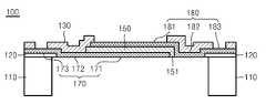
도 1은 본 발명의 일 실시예에 따른 압전형 음향 변환기의 개략적인 상면도이며, 도 2a 내지 도 2c는 도 1의 A-B선, C-D선, C-O-A선을 따라 본 압전형 음향 변환기의 측단면도이다.FIG. 1 is a schematic top view of a piezoelectric acoustic transducer according to an embodiment of the present invention, and FIGS. 2A to 2C are side cross-sectional views of a piezoelectric transducer along an AB line, a CD line, and a COA line in FIG. 1 .
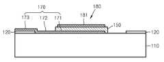
도 1 및 도 2a 내지 도 2c를 참조하면, 본 실시예의 압전형 음향 변환기(100)는, 관통영역(110a)이 형성된 기판(110)과, 상기 관통영역(110a)의 중앙쪽 일부 영역에 위치하는 압전부와, 상기 압전부의 외곽과 상기 기판(110)을 연결하는 변형막(130)을 포함한다.1 and 2A to 2C, the piezoelectric
기판(110)은 통상 사용되는 재질로 형성될 수 있으며, 예를 들어 실리콘, 유리 등으로 형성될 수 있다. 기판(110)은 관통영역(110a)을 구비한다. 상기 관통영역(110a)은 후술하는 바와 같이 압전부와 변형막(130)을 릴리즈(release)시켜 다이어프램 영역(D)을 정의한다. 관통영역(110a)은 예를 들어 원형으로 형성될 수 있다. 도 1에 도시된 참조번호 100-1은 이러한 다이어프램 영역(D)의 경계를 나타낸다.The
압전부는 관통영역(110a)의 중앙쪽 일부 영역에 위치한다. 도 1에 도시된 참조번호 100-3은 이러한 압전부의 외곽 경계를 나타낸다. The piezoelectric portion is located in a part of the central region of the
압전부는 압전막(150)과, 압전막(150)의 양면에 마련된 제1 및 제2 전극(171, 181)을 포함하는 압전 커패시턴스 구조를 가진다.The piezoelectric portion has a piezoelectric film structure including a
상기 제1 전극(171)은 제1 리드선(172) 및 제1 전극단자(173)와 함께 제1 전극부(170)를 이룬다. 상기 제1 전극단자(173)는 압전부의 외곽에 배치되며, 제1 리드선(172)는 제1 전극(171)과 제1 전극단자(173)를 전기적으로 연결한다. 상기 제1 전극(170)은 Cr, Au, Cu, Al, Mo, Ti, Pt으로 이루어진 군에서 적어도 어느 하나의 금속으로 형성될 수 있다. 예를 들어, 제1 전극(170)은 Cr/Au, Au/Cu, Al, Mo, Ti/Pt와 같은 단층 내지 다층의 금속막으로 형성될 수 있다.The
상기 압전막(150)은 상기 제1 전극(171)을 덮도록 형성될 수 있다. 즉, 상기 압전막(150)은 상기 제1 전극(171)의 영역보다 약간 넓게 상기 제1 전극(171) 위에 형성하여, 제1 전극(171)과 제2 전극(181)이 절연될 수 있도록 할 수 있다. 상기 압전막(150)은 통상의 압전형 음향 변환기에 사용되는 ZnO, AlN, PZT, PbTiO3, 또는 PLT와 같은 압전 물질로 형성될 수 있다.The
상기 제2 전극(181)은 제2 리드선(182) 및 제2 전극단자(183)와 함께 제2 전극부(180)를 이룬다. 상기 제2 전극단자(183)는 압전부의 외곽에 배치되며, 제2 리드선(182)는 제2 전극(181)과 제2 전극단자(183)를 전기적으로 연결한다. 상기 제2 전극부(180)는 예를 들어, Cr/Au, Au/Cu, Al, Mo, Ti/Pt와 같은 단층 내지 다층의 금속막으로 형성될 수 있다. 제2 전극(181)은 압전막(150)의 영역보다 약간 작게 형성할 수 있다. 제1 및 제2 전극(171, 181)은 압전막(150)을 사이에 두고 대칭되게 형성될 수 있다. 도 1에 도시된 압전부의 외곽 경계(100-3)는 압전막(150)의 외곽경계가 되며, 참조번호 100-4는 제1 및 제2 전극(171, 181)의 외곽 경계가 된다.The
변형막(130)은 압전부의 외곽과 기판(110)을 연결하며 탄성 변형되는 막이다. 변형막(130)은, 예를 들어 파릴렌(parylene)이나 저응력 비화학양론적(non-stoichiometric) 실리콘 질화막(SixNy)과 같은 물질로 형성될 수 있다. 변형막(130)의 재료로 탄성 계수가 작고 잔류 응력이 작은 물질을 사용함으로써 저주파 음성 대역에서의 특성을 향상시킬 수 있다.The
변형막(130)은 기판 접합부(131), 변형부(132), 및 압전부 접합부(133)를 포함한다. 상기 기판 접합부(131)는 기판(110)의 상면에 마련된다. 도 1에서 다이어프램의 경계(100-1)는 기판 접합부(131)의 내측 경계가 된다. 기판 접합부(131)의 제1 및 제2 전극단자(173, 183)가 위치한 영역은 외부와의 전기적 접촉을 위해 오픈된다. 상기 변형부(132), 및 압전부 접합부(133)는 기판(110)의 관통영역(110a)에 마련된다. 압전부 접합부(133)는 압전막(150) 및 제2 전극(181)의 외곽에 맞닿으며, 릴리즈된 압전부를 지지한다. 도 1에 도시된 참조번호 100-5는 압전부 접합부(133)의 내측 경계가 된다. 전술한 바와 같이 제2 전극(181)을 압전막(150)의 영역보다 약간 작게 형성하여, 압전막(150) 및 제2 전극(181)의 외곽이 단차지게 함으로써, 압전부 접합부(133)와 압전막(150)/제2 전극(181)의 결합력을 높일 수 있다. 변형부(132)는 기판 접합부(131)와 압전부 접합부(133)를 연결하며, 자유롭게 탄성 변형될 수 있다. 압전부 접합부(133)의 내측 경계(100-5) 안쪽에 변형부(132)가 연장되지 않도록 되어 있으므로, 제2 전극(181)은 외부로 노출될 수 있다.The
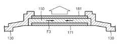
변형막(130)은 압전막(150)과 소정의 높이차(H)를 갖도록 형성된다. 이때, 높이차(H)는 변형막(130)의 기하학적 중심평면(P1)과 압전막(150)의 중심평면(P2)과의 거리에 해당된다. 즉, 상기 압전막(150)의 평면 방향 변형력의 중심선(도 3a의 F1 또는 도 4a의 F2 참조)이 상기 변형막의 기하학적 중심평면(P1)과 다른 면상에 놓이도록 한다. 변형막(130)에 있어서 동적 측면에서 볼 때 기판 접합부(131)와 압전부 접합부(133)는 무시될 수 있으므로, 변형부(132)의 기하학적 중심평면을 변형막(130)의 기하학적 중심평면(P1)으로 정의할 수 있다. 한편, 압전막(150)에는 제1 및 제2 전극단자(173, 183) 이외에 다른 막이 적층되어 있지 않다. 제1 및 제2 전극(171, 181)이 압전막(150)을 사이에 두고 대칭되게 형성된다면, 압전막(150)은 팽창 내지 수축할 뿐이고 자체적으로 휨이 발생되지는 않는다. 또한, 압전막(150) 의 두께 방향의 크기에 비해 넓이 방향의 크기가 매우 크므로, 압전막(150)의 압전 변형은 평면 방향의 팽창/수축이 주되게 된다. 즉, 제1 및 제2 전극(171, 181)에 전압이 인가되면, 압전막(150)에는 패창/수축하는 평면 방향 변형력이 발생된다. 이와 같은 압전막(150)의 평면 방향 변형력의 중심선이 놓이는 평면을 압전막(150)의 중심평면(P2)으로 정의한다. 상기와 같이 변형막(130)은 압전막(150)과 소정의 높이차(H)를 갖도록 형성하기 위하여, 예를 들어 제1 전극(171)을 변형막(130)의 두께에 대해 무시할 수 없을 정도의 두께로 형성할 수 있을 것이다.The
상기 제1 및 제2 전극단자(173, 183)와 기판(110) 사이에는 기판 절연막(120)이 개재될 수 있다. 가령, 기판(100)이 실리콘과 같은 전도성이 있는 물질로 형성된 경우, 기판 절연막(120)은 기판(110)과 제1 및 제2 전극단자(173, 183) 사이를 전기적으로 절연시킨다. 도 1에 도시된 참조번호 100-2는 기판 절연막(120)의 내측 경계를 나타낸다. 만일 기판(110)이 절연성이 있다면, 기판 절연막(120)은 생략될 수 있다.A
다음으로, 도 3a 내지 도 4b를 참조하여, 본 실시예의 압전형 음향 변환기의 동작을 설명하기로 한다.Next, the operation of the piezoelectric transducer of this embodiment will be described with reference to Figs. 3A to 4B.
도 3a 및 도 3b는, 압전막(150)에 소정의 전압이 인가되어 압전막(150)이 팽창한다고 할 때, 압전막(150)의 평면 방향의 팽창에 따른 다이어프램의 움직임을 보여준다.3A and 3B show the movement of the diaphragm in accordance with the expansion of the
전술한 바와 같이 변형막(130)의 기하학적 중심평면(P1)과 압전막(150)의 중심평면(P2)은 일치하지 않으므로, 압전막(150)에서 발생되는 팽창 변형력(F1)은 변 형막(130)의 반력(reaction force)(F2)이 동일 선상에 놓이지 않게 된다. 이와 같이 팽창 변형력(F1)은 변형막(130)의 반력(F2)이 동일 선상에 놓이지 않으므로, 팽창 변형력(F1)은 중심점(C)를 중심으로 변형부(132)를 반시계 방향(R1)으로 비트는 토크로 작용하게 된다. 결과적으로, 압전부는 도 3b에 도시되듯이 하방을 움직이게 된다.The geometric center plane P1 of the
도 4a 및 도 4b는, 압전막(150)에 소정의 전압이 인가되어 압전막(150)이 수축한다고 할 때, 압전막(150)의 평면 방향의 수축에 따른 다이어프램의 움직임을 보여준다.4A and 4B show the movement of the diaphragm in accordance with the shrinkage of the
전술한 바와 같이 변형막(130)의 기하학적 중심평면(P1)과 압전막(150)의 중심평면(P2)은 일치하지 않으므로, 압전막(150)에서 발생되는 수축 변형력(F3)은 변형막(130)의 반력(F4)이 동일 면상에 놓이지 않게 된다. 이에 따라, 수축 변형력(F3)은 중심점(C)를 중심으로 변형부(132)를 시계 방향(R2)으로 비트는 토크로 작용하게 되며, 압전부는 도 4b에 도시되듯이 상방을 움직이게 된다.Since the geometrical center plane P1 of the
상기와 같이, 압전막(150)의 팽창/수축에 따라 변형부(132)가 휘게 됨으로써 압전부를 포함한 다이어프램은 상하로 진동하게 된다. 이와 같은 진동 메커니즘은, 변형막(130)을 다이어프램의 외곽에만 사용함으로써 구조 강성을 작게 하며, 따라서 저전압 구동에서도 큰 상하 진동을 기대할 수 있다. 즉, 본 실시예의 압전형 음향 변환기에서, 압전부의 압전변형력은 압전부를 직접적으로 휘게 하지 않고 변형막에 비트는 힘으로 작용하여 다이어프램의 진동 특성을 향상시킨다.As described above, the
전술한 실시예에서는 변형막(130)의 기하학적 중심평면(P1)과 압전막(150)의 중심평면(P2)은 일치하지 않은 경우를 예로 들었으나, 본 발명의 실시예들은 이에 한정되는 것은 아니다. 예를 들어, 변형막(130)의 기하학적 중심평면(P1)과 압전막(150)의 중심평면(P2)은 일치하더라도, 압전막(150)의 잔류응력과 변형막(130)의 잔류응력이 동일 면상에 놓이지 않게 되면, 휨축(bending axis)가 일치하지 않아 편심된 압축력 또는 인장력이 작용하게 되어 변형막(150), 특히 변형부(132)의 휨이 발생될 수 있다.Although the geometric center plane P1 of the
전술한 실시예의 압전형 음향 변환기의 동작은 제1 및 제2 전극(171,181)에 전압을 인가하는 경우, 즉 마이크로 스피커인 경우를 예로 들어 설명하였다. 그러나, 압전막(150)에서의 전기적 에너지와 압전 변형 에너지의 변환은 서로 뒤바뀔 수 있으므로, 본 실시예의 압전형 음향 변환기는 외부의 진동을 전기적 에너지로 바꾸는 마이크로 폰에도 적용할 수 있음은 당해 분야의 통상의 지식을 가진 자라면 충분히 이해할 수 있을 것이다.The operation of the piezoelectric transducer of the above-described embodiment has been described by taking the case where a voltage is applied to the first and
도 5는 도 1의 압전형 음향 변환기의 변형례를 도시한다. 본 변형례의 압전형 음향 변환기는, 압전막(150)과 제2 전극(181) 사이에 압전부 절연막(190)을 더 포함한다. 이와 같이 압전부 절연막(190)을 더 구비함으로써, 파워가 큰 압전형 음향 변환기에 있어서 발생될 수 있는 압전막(150)에서의 절연파괴를 방지할 수 있다.Fig. 5 shows a modification of the piezoelectric acoustic transducer of Fig. The piezoelectric acoustic transducer according to the present modification further includes a piezoelectric insulating film 190 between the
도 6은 본 발명의 다른 실시예에 따른 압전형 음향 변환기를 도시한다.6 shows a piezoelectric acoustic transducer according to another embodiment of the present invention.
도 6을 참조하면, 본 실시예의 압전형 음향 변환기(200)는, 관통영역(210a)이 형성된 기판(210)과, 상기 관통영역(210a)의 중앙쪽 일부 영역에 위치하는 변형 막(230)과, 상기 변형막(230)의 외곽과 상기 기판(210)을 연결하는 압전부를 포함한다.6, the piezoelectric
기판(210)의 관통영역(210a)은 다이어프램을 정의하는 영역으로, 예를 들어 원형으로 형성될 수 있다.The
변형막(230)은 관통영역(210a)의 중앙쪽 일부 영역에 위치한다. 변형막(230)은 변형부(231)와 압전부 접합부(233)을 포함한다. 변형부(231)는 압전부의 팽창/수축에 따라 휨이 발생되는 영역이다. 압전부 접합부(233)는 변형부(231)와 압전부를 결합시킨다.The
압전부는 변형막(230)의 외곽으로 관통영역(210a) 내측 둘레를 따라 형성된다. 압전부는 압전막(250)과 압전막(250)의 양면에 마련된 제1 및 제2 전극(271, 281)을 포함하는 압전 커패시턴스 구조를 가진다. 변형막(230)의 기하학적 중심평면(P1′)과 압전막(250)의 중심평면(P2′)은 높이차 H′을 가진다. 제1 전극(271)은 제1 리드선(미도시) 및 제1 전극단자(273)와 함께 제1 전극부(270)를 이루며, 제2 전극(281)은 제2 리드선(282) 및 제2 전극단자(283)와 함께 제2 전극부(280)를 이룬다. 기판(210)과 제1 및 제2 전극단자(273,283) 사이에는 기판 절연막(220)이 마련될 수 있다.The piezoelectric portion is formed along the inner periphery of the through
본 실시예의 압전형 음향 변환기(200)의 진동 메커니즘은 전술한 실시예와 실질적으로 동일하다. 즉, 압전막(250)에는 전술한 실시예에서와 마찬가지로 전압이 인가됨에 따라 평면방향으로 팽창/수축하는 변형력이 발생될 수 있다. 변형막(230)의 기하학적 중심평면(P1′)과 압전막(250)의 중심평면(P2′) 사이의 높이 차 H′에 의해 압전막(250)에서 발생되는 팽창/수축하는 변형력은 변형부(231)을 비트는 토크로 작용하게 되며, 이에 따라 다이어프램을 이루는 변형막(230) 및 압전부는 상하로 진동하게 된다.The vibration mechanism of the piezoelectric
다음으로, 본 발명의 일 실시예에 따른 압전형 음향 변환기의 제조 방법을 설명하기로 한다. 도 7a 내지 도 7d는 본 발명의 일 실시예에 따른 압전형 음향 변환기의 제조 공정을 간략하게 보여주는 순서도이다.Next, a method of manufacturing the piezoelectric transducer according to an embodiment of the present invention will be described. 7A to 7D are flowcharts illustrating a manufacturing process of the piezoelectric transducer according to an embodiment of the present invention.
도 7a를 참조하면, 먼저 기판(110)을 준비한다. 기판(110)의 <100>면의 소정의 영역에 기판 절연막(120)을 형성한다. 기판(110)으로 실리콘 기판을 사용하는 경우, 기판(110)의 일면 전체에 실리콘 산화막(silicon oxide; SiO2)을 형성한 뒤 이를 패터닝하여 소정 영역에 절연막(120)을 형성할 수 있다.Referring to FIG. 7A, first, a
다음으로, 도 7b를 참조하면, 스퍼터링(sputtering)이나 진공증착(evaporation)등의 증착공정을 이용하여 Cr/Au, Au/Cu, Al, Mo, Ti/Pt와 같은 단층 내지 다층으로 금속박막을 형성하고 제1 전극(171), 제1 리드선(172), 및 제1 전극단자(173)로 패터닝하여 제1 전극부(170)를 형성한다. 다음으로, 압전막(150)을 제1 전극(171) 위에 적층한다. 압전막(150)은 제1 전극(171)보다 넓게 형성하여 제1 전극(171)을 덮도록 한다. 압전막(150)은 ZnO, AlN, PZT, PbTiO3, 또는 PLT 등으로 스퍼터링 또는 스핀-코팅(spin-coating) 등의 방법으로 증착한 후 부분 식각하여 형성할 수 있다. 다음으로, Cr/Au, Au/Cu, Al, Mo, Ti/Pt와 같은 단층 내지 다층으로 금속박막으로 제2 전극(181), 제2 리드선(도 2b의 182 참조) 및 제2 전극 단자(도 2b의 183 참조)를 포함하는 제2 전극부(180)를 형성한다. 제2 전극부(180)는 증착 및 식각 공정이나 리프트-오프(lift-off) 방법 등을 통해 형성할 수 있다. 제2 전극(181)은 압전막(150)보다 작게 형성한다.Next, referring to FIG. 7B, a metal thin film such as Cr / Au, Au / Cu, Al, Mo and Ti / Pt is formed as a single layer or multilayer by using a deposition process such as sputtering or vacuum evaporation And the
다음으로, 도 7c를 참조하면, 압전막(150) 및 제1 및 제2 전극부(170, 180) 위에 파릴렌이나 실리콘 질화물 등을 적층하고 일부 영역(130a,130b)을 선택적으로 식각하여 변형막(130)을 형성한다. 예를 들어, 파릴렌 박막의 선택적인 식각은 포토 레지스트를 식각 마스크로 사용한 O2 플라즈마 식각법을 이용할 수 있다. 변형막(130)은 압전막(150)과 소정의 높이차(H)를 갖도록 형성하기 위하여, 예를 들어 제1 전극(171)을 변형막(130)의 두께에 대해 무시할 수 없을 정도의 두께로 형성할 수 있다.7C, parylene or silicon nitride is deposited on the
다음으로, 도 7d를 참조하면, 기판(110)의 후면의 다이어프램 영역을 변형막의 일부 및 압전부의 저면이 노출될 때까지 식각하여 기판(110)에 관통영역(110a)을 형성한다. 기판(110)의 후면의 식각은 예를 들어, 실리콘 기판에 대해 실리콘 딥 식각법(Si Deep ICP RIE)을 이용할 수 있다. 이와 같이 변형막의 및 압전부를 릴리즈시킴으로써 다이어프램을 완성한다.7D, the diaphragm region on the rear surface of the
이러한 본 발명인 압전형 음향 변환기 및 이의 제조방법은 이해를 돕기 위하여 도면에 도시된 실시예를 참고로 설명되었으나, 이는 예시적인 것에 불과하며, 당해 분야에서 통상적 지식을 가진 자라면 이로부터 다양한 변형 및 균등한 타 실시예가 가능하다는 점을 이해할 것이다. 따라서, 본 발명의 진정한 기술적 보호 범 위는 첨부된 특허청구범위에 의해 정해져야 할 것이다.The piezoelectric transducer and the method of manufacturing the piezoelectric transducer of the present invention have been described with reference to the embodiments shown in the drawings for the sake of understanding. However, those skilled in the art will appreciate that various modifications, It will be appreciated that other embodiments are possible. Accordingly, the true scope of protection of the present invention should be defined by the appended claims.
도 1은 본 발명의 일 실시예에 따른 압전형 음향 변환기의 개략적인 상면도이다.1 is a schematic top view of a piezoelectric acoustic transducer according to an embodiment of the present invention.
도 2a 내지 도 2c는 도 1의 A-B선, C-D선, C-O-A선을 따라 본 압전형 음향 변환기의 측단면도이다.2A to 2C are side cross-sectional views of the piezoelectric type acoustic transducer along the lines A-B, C-D, and C-O-A in Fig.
도 3a 내지 도 4b는 도 1의 압전형 음향 변환기의 동작을 설명하는 도면이다.3A to 4B are views for explaining the operation of the piezoelectric type acoustic transducer of FIG.
도 5는 도 1의 압전형 음향 변환기의 변형례를 도시한다.Fig. 5 shows a modification of the piezoelectric acoustic transducer of Fig.
도 6은 본 발명의 다른 실시예에 따른 압전형 음향 변환기의 개략적인 측면도이다.6 is a schematic side view of a piezoelectric acoustic transducer according to another embodiment of the present invention.
도 7a 내지 도 7d는 본 발명의 일 실시예에 따른 압전형 음향 변환기의 제조 방법을 설명하는 순서도이다.7A to 7D are flowcharts illustrating a method of manufacturing a piezoelectric acoustic transducer according to an embodiment of the present invention.
<도면의 주요부분에 대한 부호의 설명>Description of the Related Art
100, 101, 200...압전형 음향 변환기100, 101, 200 ... Piezoelectric acoustic transducer
110, 210...기판120, 185, 220...절연막110 and 210, a
130, 230...변형막150, 250...압전막130, 230 ...
170, 270...제1전극부180, 280...제2전극부170, 270 ...
Claims (17)
Translated fromKoreanPriority Applications (4)
| Application Number | Priority Date | Filing Date | Title |
|---|---|---|---|
| KR1020080130385AKR101545271B1 (en) | 2008-12-19 | 2008-12-19 | Piezoelectric acoustic transducer and method for fabricating the same |
| US12/489,531US8237332B2 (en) | 2008-12-19 | 2009-06-23 | Piezoelectric acoustic transducer and method of fabricating the same |
| CN200910224400.XACN101754077B (en) | 2008-12-19 | 2009-12-02 | Piezoelectric acoustic transducer and method for fabricating the same |
| JP2009280707AJP5486913B2 (en) | 2008-12-19 | 2009-12-10 | Piezoelectric acoustic transducer and manufacturing method thereof |
Applications Claiming Priority (1)
| Application Number | Priority Date | Filing Date | Title |
|---|---|---|---|
| KR1020080130385AKR101545271B1 (en) | 2008-12-19 | 2008-12-19 | Piezoelectric acoustic transducer and method for fabricating the same |
Related Child Applications (1)
| Application Number | Title | Priority Date | Filing Date |
|---|---|---|---|
| KR1020150044552ADivisionKR101652784B1 (en) | 2015-03-30 | 2015-03-30 | Piezoelectric acoustic transducer and method for fabricating the same |
Publications (2)
| Publication Number | Publication Date |
|---|---|
| KR20100071607A KR20100071607A (en) | 2010-06-29 |
| KR101545271B1true KR101545271B1 (en) | 2015-08-19 |
Family
ID=42264968
Family Applications (1)
| Application Number | Title | Priority Date | Filing Date |
|---|---|---|---|
| KR1020080130385AActiveKR101545271B1 (en) | 2008-12-19 | 2008-12-19 | Piezoelectric acoustic transducer and method for fabricating the same |
Country Status (4)
| Country | Link |
|---|---|
| US (1) | US8237332B2 (en) |
| JP (1) | JP5486913B2 (en) |
| KR (1) | KR101545271B1 (en) |
| CN (1) | CN101754077B (en) |
Cited By (5)
| Publication number | Priority date | Publication date | Assignee | Title |
|---|---|---|---|---|
| US10313797B2 (en) | 2016-09-09 | 2019-06-04 | Hyundai Motor Company | Microphone, manufacturing method and control method thereof |
| US11832057B2 (en) | 2019-08-13 | 2023-11-28 | Skyworks Solutions, Inc. | Piezoelectric MEMS microphone |
| US12329033B2 (en) | 2021-10-21 | 2025-06-10 | Skyworks Solutions, Inc. | Piezoelectric sensor with increased sensitivity and devices having the same |
| US12335687B2 (en) | 2021-09-20 | 2025-06-17 | Skyworks Solutions, Inc. | Piezoelectric MEMS microphone with cantilevered separation |
| US12391546B1 (en) | 2021-01-07 | 2025-08-19 | Skyworks Global Pte. Ltd. | Method of making acoustic devices with directional reinforcement |
Families Citing this family (26)
| Publication number | Priority date | Publication date | Assignee | Title |
|---|---|---|---|---|
| KR101520070B1 (en) | 2008-09-22 | 2015-05-14 | 삼성전자 주식회사 | Piezoelectric microspeaker and its fabrication method |
| KR101562339B1 (en) | 2008-09-25 | 2015-10-22 | 삼성전자 주식회사 | Piezoelectric microspeaker and its fabrication method |
| US8363864B2 (en) | 2008-09-25 | 2013-01-29 | Samsung Electronics Co., Ltd. | Piezoelectric micro-acoustic transducer and method of fabricating the same |
| KR101561660B1 (en) | 2009-09-16 | 2015-10-21 | 삼성전자주식회사 | Piezoelectric micro speaker having annular ring-shape vibrating membrane and method of manufacturing the same |
| KR101561661B1 (en)* | 2009-09-25 | 2015-10-21 | 삼성전자주식회사 | Piezoelectric micro speaker with mass attached to diaphragm and method of manufacturing the same |
| JP6041382B2 (en)* | 2010-07-23 | 2016-12-07 | 日本電気株式会社 | Audio equipment and oscillation unit |
| US8465659B2 (en)* | 2011-01-21 | 2013-06-18 | Xerox Corporation | Polymer layer removal on pzt arrays using a plasma etch |
| US8811636B2 (en) | 2011-11-29 | 2014-08-19 | Qualcomm Mems Technologies, Inc. | Microspeaker with piezoelectric, metal and dielectric membrane |
| EP2973767B1 (en)* | 2013-03-14 | 2017-11-22 | Volcano Corporation | Method of coating wafer-scale transducer |
| FR3022674B1 (en)* | 2014-06-18 | 2019-12-13 | Iem Sarl | DETECTION TERMINAL COMPRISING A PIEZOELECTRIC TRANSDUCER ATTACHED TO A MEMBRANE LINKED TO A STOP STRUCTURE |
| KR101550636B1 (en)* | 2014-09-23 | 2015-09-07 | 현대자동차 주식회사 | Micro phone and method manufacturing the same |
| JP6536792B2 (en)* | 2015-03-25 | 2019-07-03 | セイコーエプソン株式会社 | Ultrasonic sensor and method of manufacturing the same |
| DE102015224770A1 (en)* | 2015-12-10 | 2017-06-14 | Robert Bosch Gmbh | Sound transducer arrangement with annular first connecting regions and method for producing a sound transducer arrangement with annular first connecting regions |
| TWI708511B (en) | 2016-07-21 | 2020-10-21 | 聯華電子股份有限公司 | Piezoresistive microphone and method of fabricating the same |
| CN108140373B (en)* | 2016-09-28 | 2021-10-26 | 株式会社村田制作所 | Piezoelectric sound producing component and method for manufacturing same |
| KR101903420B1 (en)* | 2016-10-07 | 2018-11-02 | 성균관대학교산학협력단 | Microphone and method of fabricating thereof |
| DE102017205375A1 (en)* | 2017-03-30 | 2018-10-04 | Robert Bosch Gmbh | transducer |
| CN107071672B (en)* | 2017-05-22 | 2020-08-21 | 潍坊歌尔微电子有限公司 | Piezoelectric microphone |
| DE102018126387A1 (en)* | 2018-10-23 | 2020-04-23 | Tdk Electronics Ag | Sound transducer and method for operating the sound transducer |
| CN110040681A (en)* | 2019-03-05 | 2019-07-23 | 常州元晶电子科技有限公司 | A kind of production method of the high consistency MEMS PZT (piezoelectric transducer) of low cost |
| CN110677784A (en)* | 2019-09-29 | 2020-01-10 | 歌尔股份有限公司 | Loudspeaker of sound cone and applied this sound cone |
| CN110896518B (en)* | 2019-12-17 | 2021-03-12 | 安徽奥飞声学科技有限公司 | Manufacturing method of MEMS structure |
| CN111182430B (en)* | 2019-12-17 | 2024-10-08 | 安徽奥飞声学科技有限公司 | MEMS structure |
| CN113573218B (en)* | 2020-04-29 | 2022-10-18 | 华为技术有限公司 | Piezoelectric acoustic sensor and method of making the same |
| US12267646B2 (en)* | 2023-02-16 | 2025-04-01 | AAC Technologies Pte. Ltd. | Acoustic transducer and method for manufacturing acoustic transducer |
| CN116916228A (en)* | 2023-08-11 | 2023-10-20 | 湖北九峰山实验室 | Piezoelectric MEMS sounder and manufacturing method thereof |
Citations (2)
| Publication number | Priority date | Publication date | Assignee | Title |
|---|---|---|---|---|
| US20040256953A1 (en)* | 2003-06-20 | 2004-12-23 | Ngk Insulators, Ltd. | Piezoelectric/electrostrictive device made of piezoelectric/electrostrictive film and manufacturing method |
| JP2006100954A (en)* | 2004-09-28 | 2006-04-13 | Matsushita Electric Ind Co Ltd | Piezoelectric acoustic transducer and manufacturing method thereof |
Family Cites Families (20)
| Publication number | Priority date | Publication date | Assignee | Title |
|---|---|---|---|---|
| JPS5772497A (en)* | 1980-10-23 | 1982-05-06 | Murata Mfg Co Ltd | Piezoelectric speaker |
| JPH0833097A (en)* | 1994-07-13 | 1996-02-02 | Olympus Optical Co Ltd | Piezoelectric element |
| JP2001119795A (en)* | 1999-08-10 | 2001-04-27 | Murata Mfg Co Ltd | Piezoelectric electroacoustic transducer |
| WO2001022776A1 (en) | 1999-09-21 | 2001-03-29 | University Of Hawaii | Method of forming parylene-diaphragm piezoelectric acoustic transducers |
| US6726618B2 (en)* | 2001-04-12 | 2004-04-27 | Otologics, Llc | Hearing aid with internal acoustic middle ear transducer |
| US7003125B2 (en)* | 2001-09-12 | 2006-02-21 | Seung-Hwan Yi | Micromachined piezoelectric microspeaker and fabricating method thereof |
| KR100416164B1 (en) | 2002-01-21 | 2004-01-24 | 이승환 | Manufacturing method and piezoelectric bimorph microphone |
| KR100416158B1 (en) | 2002-01-21 | 2004-01-28 | 이승환 | Method for fabricating a compressive thin film diaphragm and piezoelectric microspeaker fabricated therewith |
| JP3945292B2 (en)* | 2002-04-10 | 2007-07-18 | 松下電器産業株式会社 | Diaphragm type transducer |
| KR100512960B1 (en) | 2002-09-26 | 2005-09-07 | 삼성전자주식회사 | Flexible MEMS transducer and its manufacturing method, and flexible MEMS wireless microphone |
| JP3988672B2 (en)* | 2003-04-07 | 2007-10-10 | 株式会社村田製作所 | Piezoelectric electroacoustic transducer and manufacturing method thereof |
| CN1677842B (en)* | 2004-03-31 | 2011-06-08 | 松下电器产业株式会社 | Acoustic resonator and filter |
| JP4280198B2 (en)* | 2004-04-30 | 2009-06-17 | 株式会社東芝 | Thin film piezoelectric resonator |
| CN101336562B (en)* | 2005-12-27 | 2012-11-28 | 日本电气株式会社 | Piezoelectric actuator and electronic device |
| JP4321552B2 (en)* | 2006-06-07 | 2009-08-26 | セイコーエプソン株式会社 | Actuator device and liquid jet head |
| KR100791084B1 (en) | 2006-06-27 | 2008-01-03 | 충주대학교 산학협력단 | Piezoelectric micro speaker and manufacturing method thereof |
| JP4215788B2 (en)* | 2006-08-25 | 2009-01-28 | ホシデン株式会社 | Piezoelectric electroacoustic transducer |
| US7963640B2 (en)* | 2006-09-08 | 2011-06-21 | Canon Kabushiki Kaisha | Liquid discharge head and method for manufacturing the liquid discharge head |
| WO2008056800A1 (en)* | 2006-11-09 | 2008-05-15 | Nec Corporation | Piezoelectric speaker and electronic apparatus with piezoelectric speaker |
| KR100870148B1 (en) | 2007-02-02 | 2008-11-24 | 충주대학교 산학협력단 | Low Voltage Driven Piezoelectric Microspeakers and Manufacturing Method Thereof |
- 2008
- 2008-12-19KRKR1020080130385Apatent/KR101545271B1/enactiveActive
- 2009
- 2009-06-23USUS12/489,531patent/US8237332B2/enactiveActive
- 2009-12-02CNCN200910224400.XApatent/CN101754077B/enactiveActive
- 2009-12-10JPJP2009280707Apatent/JP5486913B2/enactiveActive
Patent Citations (2)
| Publication number | Priority date | Publication date | Assignee | Title |
|---|---|---|---|---|
| US20040256953A1 (en)* | 2003-06-20 | 2004-12-23 | Ngk Insulators, Ltd. | Piezoelectric/electrostrictive device made of piezoelectric/electrostrictive film and manufacturing method |
| JP2006100954A (en)* | 2004-09-28 | 2006-04-13 | Matsushita Electric Ind Co Ltd | Piezoelectric acoustic transducer and manufacturing method thereof |
Cited By (5)
| Publication number | Priority date | Publication date | Assignee | Title |
|---|---|---|---|---|
| US10313797B2 (en) | 2016-09-09 | 2019-06-04 | Hyundai Motor Company | Microphone, manufacturing method and control method thereof |
| US11832057B2 (en) | 2019-08-13 | 2023-11-28 | Skyworks Solutions, Inc. | Piezoelectric MEMS microphone |
| US12391546B1 (en) | 2021-01-07 | 2025-08-19 | Skyworks Global Pte. Ltd. | Method of making acoustic devices with directional reinforcement |
| US12335687B2 (en) | 2021-09-20 | 2025-06-17 | Skyworks Solutions, Inc. | Piezoelectric MEMS microphone with cantilevered separation |
| US12329033B2 (en) | 2021-10-21 | 2025-06-10 | Skyworks Solutions, Inc. | Piezoelectric sensor with increased sensitivity and devices having the same |
Also Published As
| Publication number | Publication date |
|---|---|
| CN101754077B (en) | 2014-06-04 |
| CN101754077A (en) | 2010-06-23 |
| KR20100071607A (en) | 2010-06-29 |
| US8237332B2 (en) | 2012-08-07 |
| US20100156238A1 (en) | 2010-06-24 |
| JP5486913B2 (en) | 2014-05-07 |
| JP2010148102A (en) | 2010-07-01 |
Similar Documents
| Publication | Publication Date | Title |
|---|---|---|
| KR101545271B1 (en) | Piezoelectric acoustic transducer and method for fabricating the same | |
| JP5513287B2 (en) | Piezoelectric microspeaker having piston diaphragm and manufacturing method thereof | |
| US8509462B2 (en) | Piezoelectric micro speaker including annular ring-shaped vibrating membranes and method of manufacturing the piezoelectric micro speaker | |
| KR101561661B1 (en) | Piezoelectric micro speaker with mass attached to diaphragm and method of manufacturing the same | |
| US11905164B2 (en) | Micro-electro-mechanical system acoustic sensor, micro-electro-mechanical system package structure and method for manufacturing the same | |
| KR100931575B1 (en) | Piezoelectric element micro speaker using MEMS and its manufacturing method | |
| JP3700559B2 (en) | Piezoelectric acoustic component and manufacturing method thereof | |
| US6741710B1 (en) | Piezoelectric electroacoustic transducer | |
| KR100931578B1 (en) | Piezoelectric element microphone, speaker, microphone-speaker integrated device and manufacturing method thereof | |
| US8401220B2 (en) | Piezoelectric micro speaker with curved lead wires and method of manufacturing the same | |
| US20230234837A1 (en) | Mems microphone with an anchor | |
| KR20080034407A (en) | Electrostatic pressure transducer and manufacturing method thereof | |
| US20230239641A1 (en) | Method of making mems microphone with an anchor | |
| US11239408B2 (en) | Acoustic transducer and related fabrication and packaging techniques | |
| WO2011024397A1 (en) | Capacitor microphone | |
| KR101652784B1 (en) | Piezoelectric acoustic transducer and method for fabricating the same | |
| KR101066102B1 (en) | Micro speaker and its manufacturing method | |
| JP2011139267A (en) | Piezoelectric type sounding device | |
| KR20040091207A (en) | Piezoelectric acoustic transducer and manufacturing method thereof | |
| CN115767385A (en) | MEMS (micro-electromechanical systems) loudspeaker, electronic equipment and preparation method of MEMS loudspeaker | |
| CN117499848A (en) | MEMS piezoelectric loudspeaker and preparation method thereof | |
| WO2023176271A1 (en) | Transducer and method for manufacturing same | |
| CN117714963A (en) | MEMS speaker with stretchable membrane, manufacturing method thereof, and electronic device including same | |
| CN120416749A (en) | A fixed-end beam-cantilever beam piezoelectric MEMS speaker and its preparation method and application | |
| JP2012151583A (en) | Piezoelectric type actuator |
Legal Events
| Date | Code | Title | Description |
|---|---|---|---|
| PA0109 | Patent application | St.27 status event code:A-0-1-A10-A12-nap-PA0109 | |
| PG1501 | Laying open of application | St.27 status event code:A-1-1-Q10-Q12-nap-PG1501 | |
| R18-X000 | Changes to party contact information recorded | St.27 status event code:A-3-3-R10-R18-oth-X000 | |
| A201 | Request for examination | ||
| PA0201 | Request for examination | St.27 status event code:A-1-2-D10-D11-exm-PA0201 | |
| D13-X000 | Search requested | St.27 status event code:A-1-2-D10-D13-srh-X000 | |
| D14-X000 | Search report completed | St.27 status event code:A-1-2-D10-D14-srh-X000 | |
| E902 | Notification of reason for refusal | ||
| PE0902 | Notice of grounds for rejection | St.27 status event code:A-1-2-D10-D21-exm-PE0902 | |
| AMND | Amendment | ||
| P11-X000 | Amendment of application requested | St.27 status event code:A-2-2-P10-P11-nap-X000 | |
| P13-X000 | Application amended | St.27 status event code:A-2-2-P10-P13-nap-X000 | |
| E601 | Decision to refuse application | ||
| PE0601 | Decision on rejection of patent | St.27 status event code:N-2-6-B10-B15-exm-PE0601 | |
| A107 | Divisional application of patent | ||
| AMND | Amendment | ||
| J201 | Request for trial against refusal decision | ||
| P11-X000 | Amendment of application requested | St.27 status event code:A-2-2-P10-P11-nap-X000 | |
| P13-X000 | Application amended | St.27 status event code:A-2-2-P10-P13-nap-X000 | |
| PA0107 | Divisional application | St.27 status event code:A-0-1-A10-A18-div-PA0107 St.27 status event code:A-0-1-A10-A16-div-PA0107 | |
| PJ0201 | Trial against decision of rejection | St.27 status event code:A-3-3-V10-V11-apl-PJ0201 | |
| PB0901 | Examination by re-examination before a trial | St.27 status event code:A-6-3-E10-E12-rex-PB0901 | |
| B701 | Decision to grant | ||
| PB0701 | Decision of registration after re-examination before a trial | St.27 status event code:A-3-4-F10-F13-rex-PB0701 | |
| GRNT | Written decision to grant | ||
| PR0701 | Registration of establishment | St.27 status event code:A-2-4-F10-F11-exm-PR0701 | |
| PR1002 | Payment of registration fee | St.27 status event code:A-2-2-U10-U11-oth-PR1002 Fee payment year number:1 | |
| PG1601 | Publication of registration | St.27 status event code:A-4-4-Q10-Q13-nap-PG1601 | |
| P22-X000 | Classification modified | St.27 status event code:A-4-4-P10-P22-nap-X000 | |
| P22-X000 | Classification modified | St.27 status event code:A-4-4-P10-P22-nap-X000 | |
| FPAY | Annual fee payment | Payment date:20180718 Year of fee payment:4 | |
| PR1001 | Payment of annual fee | St.27 status event code:A-4-4-U10-U11-oth-PR1001 Fee payment year number:4 | |
| PR1001 | Payment of annual fee | St.27 status event code:A-4-4-U10-U11-oth-PR1001 Fee payment year number:5 | |
| PR1001 | Payment of annual fee | St.27 status event code:A-4-4-U10-U11-oth-PR1001 Fee payment year number:6 | |
| PR1001 | Payment of annual fee | St.27 status event code:A-4-4-U10-U11-oth-PR1001 Fee payment year number:7 | |
| PR1001 | Payment of annual fee | St.27 status event code:A-4-4-U10-U11-oth-PR1001 Fee payment year number:8 | |
| PR1001 | Payment of annual fee | St.27 status event code:A-4-4-U10-U11-oth-PR1001 Fee payment year number:9 | |
| PR1001 | Payment of annual fee | St.27 status event code:A-4-4-U10-U11-oth-PR1001 Fee payment year number:10 | |
| PR1001 | Payment of annual fee | St.27 status event code:A-4-4-U10-U11-oth-PR1001 Fee payment year number:11 |