KR101541812B1 - Nonvolatile memory device - Google Patents
Nonvolatile memory deviceDownload PDFInfo
- Publication number
- KR101541812B1 KR101541812B1KR1020080115151AKR20080115151AKR101541812B1KR 101541812 B1KR101541812 B1KR 101541812B1KR 1020080115151 AKR1020080115151 AKR 1020080115151AKR 20080115151 AKR20080115151 AKR 20080115151AKR 101541812 B1KR101541812 B1KR 101541812B1
- Authority
- KR
- South Korea
- Prior art keywords
- data
- memory cell
- block
- memory device
- read command
- Prior art date
- Legal status (The legal status is an assumption and is not a legal conclusion. Google has not performed a legal analysis and makes no representation as to the accuracy of the status listed.)
- Expired - Fee Related
Links
Images


Classifications
- G—PHYSICS
- G11—INFORMATION STORAGE
- G11C—STATIC STORES
- G11C16/00—Erasable programmable read-only memories
- G11C16/02—Erasable programmable read-only memories electrically programmable
- G11C16/06—Auxiliary circuits, e.g. for writing into memory
- G11C16/26—Sensing or reading circuits; Data output circuits
- G—PHYSICS
- G11—INFORMATION STORAGE
- G11C—STATIC STORES
- G11C16/00—Erasable programmable read-only memories
- G11C16/02—Erasable programmable read-only memories electrically programmable
- G11C16/06—Auxiliary circuits, e.g. for writing into memory
- G11C16/34—Determination of programming status, e.g. threshold voltage, overprogramming or underprogramming, retention
- G11C16/3436—Arrangements for verifying correct programming or erasure
- G11C16/3454—Arrangements for verifying correct programming or for detecting overprogrammed cells
- G—PHYSICS
- G11—INFORMATION STORAGE
- G11C—STATIC STORES
- G11C16/00—Erasable programmable read-only memories
- G11C16/02—Erasable programmable read-only memories electrically programmable
- G11C16/06—Auxiliary circuits, e.g. for writing into memory
- G11C16/34—Determination of programming status, e.g. threshold voltage, overprogramming or underprogramming, retention
- G11C16/3436—Arrangements for verifying correct programming or erasure
- G11C16/3454—Arrangements for verifying correct programming or for detecting overprogrammed cells
- G11C16/3459—Circuits or methods to verify correct programming of nonvolatile memory cells
Landscapes
- Read Only Memory (AREA)
Abstract
Translated fromKoreanDescription
Translated fromKorean본 발명은 비휘발성 메모리 장치에 관한 것으로, 보다 상세하게는 ISPP(Incremental Step Pulse Program) 방식에 따라 프로그램 동작을 수행하는 비휘발성 메모리 장치에 관한 것이다.The present invention relates to a nonvolatile memory device, and more particularly, to a nonvolatile memory device that performs a program operation according to an Incremental Step Pulse Program (ISPP) method.
반도체 메모리 장치(semiconductor memory device)는 데이터를 저장해 두고 필요할 때 꺼내어 읽어볼 수 있는 기억장치이다. 반도체 메모리 장치는 크게 램(Random Access Memory; RAM)과 롬(Read Only Memory; ROM)으로 나눌 수 있다.A semiconductor memory device is a storage device that can store data and retrieve it when needed. Semiconductor memory devices can be roughly classified into a random access memory (RAM) and a read only memory (ROM).
램(RAM)은 전원이 끊어지면 저장된 데이터가 소멸하는 휘발성 메모리 장치(volatile memory device)이다. 롬(ROM)은 전원이 끊어지더라도 저장된 데이터가 소멸하지 않는 비휘발성 메모리 장치(nonvolatile memory device)이다. 램(RAM)은 DRAM(Dynamic RAM), SRAM(Static RAM) 등을 포함한다. 롬(ROM)은 PROM(Programmable ROM), EPROM(Erasable PROM), EEPROM(Electrically EPROM), 플래시 메모리 장치(flash memory device) 등을 포함한다.RAM is a volatile memory device in which stored data is lost when power is lost. A ROM is a nonvolatile memory device that does not lose stored data even when the power is turned off. The RAM includes dynamic RAM (DRAM), static random access memory (SRAM), and the like. The ROM includes a programmable ROM (PROM), an erasable PROM (EPROM), an electrically erasable programmable ROM (EEPROM), a flash memory device, and the like.
예컨대, 플래시 메모리 장치는 소비 전력이 작고, 정보의 입출력이 자유로워 디지털카메라, 휴대폰, PDA 등 이동기기에 적합하다. 플래시 메모리 장치는 메모리 셀 어레이의 구조에 따라 낸드(NAND)형과 노어(NOR)형으로 크게 나누어진다. 낸드 플래시 메모리 장치는 주로 USB 저장장치, MP3 플레이어 등에 쓰이는 데이터 저장형 메모리 장치이다. 반면에, 노어 플래시 메모리 장치는 코드 저장형 메모리 장치로서, 처리 속도가 빠르므로 고속 데이터 처리를 요하는 이동전화 단말기 등에 많이 쓰이고 있다.For example, the flash memory device is suitable for a mobile device such as a digital camera, a mobile phone, and a PDA because of low power consumption and free input / output of information. The flash memory device is largely divided into a NAND type and a NOR type according to the structure of a memory cell array. The NAND flash memory device is a data storage type memory device mainly used for a USB storage device, an MP3 player, and the like. On the other hand, the NOR flash memory device is a code storage type memory device and is often used in mobile phone terminals requiring high-speed data processing because of its high processing speed.
최근 플래시 메모리 장치에 있어서, 메모리 셀의 워드 라인에 인가되는 전압을 단계적으로 증가시키면서 메모리 셀을 프로그램하는 ISPP(Incremental Step Pulse Program) 방식이 많이 이용되고 있다. 이때, FN 터널링(Fowler Nordheim tunneling)을 이용하여 메모리 셀을 프로그램하는 방식에 따르면 라이트 버퍼(write buffer) 사이즈는 크고 센스 엠프(sense amplifier)를 이용하여 리드할 수 있는 데이터 양은 적다.In recent flash memory devices, an ISPP (Incremental Step Pulse Program) method for programming a memory cell while gradually increasing a voltage applied to a word line of the memory cell is widely used. At this time, according to the method of programming the memory cell using FN tunneling, the size of the write buffer is large and the amount of data that can be read using the sense amplifier is small.
그러므로 메모리 셀에 대한 검증(verify) 동작 수행 시 센스 엠프를 이용하여 리드된 데이터를 이용하여 라이트 버퍼를 업데이트하기 위해서는 많은 시간이 소요되는 문제점이 있다. 또한, 데이터 리드 타임과 라이터 버퍼 업데이트 타임이 분리되어 있기 때문에 ISPP 수행 시 리드 & 업데이트 시간 소요로 인하여 전체 프로그램 시간이 증가하는 문제점이 있다.Therefore, it takes a lot of time to update the write buffer using the read data using the sense amplifier when performing a verify operation on the memory cell. In addition, since the data read time and the writer buffer update time are separated, there is a problem that the total program time is increased due to the lead & update time in ISPP execution.
따라서 본 발명이 이루고자 하는 기술적인 과제는 메모리 셀이 프로그램되었는지 여부를 검증하는데 소요되는 시간을 감소시킴으로써 프로그램 시간을 감소시킬 수 있는 비휘발성 메모리 장치를 제공하는 것이다.SUMMARY OF THE INVENTION Accordingly, it is an object of the present invention to provide a nonvolatile memory device capable of reducing program time by reducing the time required to verify whether a memory cell has been programmed.
상기 기술적 과제를 달성하기 위한 비휘발성 메모리 장치는 센스 엠프 회로, 라이트 드라이버 회로, 및 검증 블락을 포함할 수 있다. 상기 센스 엠프 회로는 리드 명령에 응답하여 비트 라인을 통하여 메모리 셀로부터 제1 데이터를 센싱하고 상기 센싱된 제1 데이터를 출력할 수 있다. 상기 라이트 드라이버 회로는 프로그램 명령에 응답하여 상기 메모리 셀을 프로그램하고 상기 메모리 셀의 프로그램 여부를 나타내는 제2 데이터를 저장할 수 있다.The nonvolatile memory device may include a sense amplifier circuit, a write driver circuit, and a verify block. The sense amplifier circuit may sense the first data from the memory cell through the bit line and output the sensed first data in response to the read command. The write driver circuit may program the memory cell in response to a program command and store second data indicating whether the memory cell is programmed.
상기 검증 블락은 제1 리드 명령에 응답하여 제1 데이터 및 상기 제2 데이터 사이의 비교 결과를 출력하고, 상기 제1 리드 명령에 연속되는 제2 리드 명령에 응답하여 판단되는 상기 메모리 셀의 프로그램 여부에 기초하여 상기 제2 데이터를 업데이트할 수 있다.Wherein the verification block outputs a comparison result between the first data and the second data in response to the first read command and determines whether the memory cell is programmed in response to a second read command successive to the first read command To update the second data.
상기 센스 엠프 회로는 상기 메모리 셀에 저장된 상기 제1 데이터를 센싱하기 위한 센스 엠프 및 상기 제1 데이터를 선택적으로 출력하기 위한 적어도 하나의 제1 스위칭 소자를 포함할 수 있다. 상기 라이트 드라이버 회로는 상기 제2 데이터를 저장하는 라이트 버퍼 및 상기 검증 블락으로부터 출력되는 데이터를 선택적으 로 상기 라이트 버퍼로 출력하기 위한 적어도 하나의 제2 스위칭 소자를 포함할 수 있다.The sense amplifier circuit may include a sense amplifier for sensing the first data stored in the memory cell and at least one first switching device for selectively outputting the first data. The write driver circuit may include a write buffer for storing the second data and at least one second switching element for selectively outputting data output from the verify block to the write buffer.
상기 검증 블락은 상기 제1 데이터와 상기 제2 데이터의 비교 결과를 출력하기 위한 비교 블락 및 상기 제1 데이터의 논리 값 및 제어 신호에 기초하여 상기 제1 데이터를 선택적으로 상기 라이트 버퍼로 출력하기 위한 제어 블락을 포함할 수 있다. 상기 비교 블락은 상기 제1 데이터 및 제2 데이터에 대한 논리 합을 수행하는 논리 게이트를 포함할 수 있다.Wherein the verification block includes a comparison block for outputting a comparison result of the first data and the second data and a comparison block for outputting the first data selectively to the write buffer based on the logical value of the first data and the control signal Control block. The comparison block may include a logic gate for performing a logical sum of the first data and the second data.
상기 제어 블락은 상기 제1 데이터의 논리 값이 제1 논리 값이고 상기 제어 신호가 활성화되면 상기 제1 데이터를 상기 라이트 버퍼로 출력하고 상기 제2 데이터의 논리 값이 제2 논리 값이면 상기 제1 데이터가 상기 라이트 버퍼로 출력되는 것을 차단할 수 있다. 상기 제어 블락은 상기 제1 데이터의 논리 값에 기초하여 상기 제1 데이터를 선택적으로 출력하는 제1 제어 블락 및 상기 제어 신호에 응답하여 상기 제1 제어 블락으로부터 출력되는 제1 데이터를 선택적으로 상기 라이트 버퍼로 출력하는 제2 제어 블락을 포함할 수 있다.Wherein the control block outputs the first data to the write buffer when the logic value of the first data is a first logic value and the control signal is activated and outputs the first data to the write buffer when the logic value of the second data is a second logic value, It is possible to prevent the data from being output to the write buffer. Wherein the control block includes a first control block for selectively outputting the first data based on a logical value of the first data and a second control block for selectively outputting the first data output from the first control block in response to the control signal, And outputting the second control block to the buffer.
상기 비휘발성 메모리 장치가 검증 동작을 수행하는 경우에 상기 리드 명령의 활성화 구간, 상기 적어도 하나의 제1 스위칭 소자의 단락 구간, 상기 적어도 하나의 제2 스위치 소자의 단락 구간은 서로 동일하며, 상기 제어 신호의 활성화 구간은 상기 제2 리드 명령의 활성화 구간에 포함될 수 있다.Wherein the activation period of the read command, the shorting interval of the at least one first switching element, and the shorting interval of the at least one second switching element are equal to each other when the nonvolatile memory device performs the verification operation, The activation period of the signal may be included in the activation period of the second read command.
상기 제1 제어 블락 및 제2 제어 블락 각각은 상기 제1 데이터의 논리 값 및 상기 제어 신호에 응답하여 스위칭되는 상기 제3 스위칭 소자 및 제4 스위칭 소자 를 포함할 수 있다. 상기 제1 제어 블락 및 제2 제어 블락 각각은 상기 제1 데이터의 논리 값 및 상기 제어 신호에 응답하여 구동되는 제1 버퍼 및 제2 버퍼를 포함할 수도 있다.Each of the first control block and the second control block may include the third switching element and the fourth switching element which are switched in response to the logical value of the first data and the control signal. Each of the first control block and the second control block may include a first buffer and a second buffer driven in response to the logical value of the first data and the control signal.
상술한 바와 같이 본 발명의 실시예에 따른 비휘발성 메모리 장치는 메모리 셀에 대한 검증 동작에 소요되는 시간을 감소시킴으로써 전체 프로그램 시간을 감소시킬 수 있으며 검증 동작에 대한 별도의 저장 수단을 필요로 하지 않는 효과가 있다.As described above, the nonvolatile memory device according to the embodiment of the present invention can reduce the total program time by reducing the time required for the verify operation on the memory cell and does not require separate storage means for the verify operation It is effective.
본 발명과 본 발명의 동작상의 이점 및 발명의 실시에 의하여 달성되는 목적을 충분히 이해하기 위해서는 본 발명의 바람직한 실시 예를 예시하는 첨부 도면 및 첨부 도면에 기재된 내용을 참조하여야만 한다.In order to fully understand the present invention, the operational advantages of the present invention and the objects achieved by the practice of the present invention, reference should be made to the accompanying drawings and the accompanying drawings which illustrate preferred embodiments of the present invention.
본 명세서에 있어서는 어느 하나의 구성요소가 다른 구성요소로 데이터 또는 신호를 '전송'하는 경우에는 상기 구성요소는 상기 다른 구성요소로 직접 상기 데이터 또는 신호를 전송할 수 있고, 적어도 하나의 또 다른 구성요소를 통하여 상기 데이터 또는 신호를 상기 다른 구성요소로 전송할 수 있음을 의미한다.In the present specification, when one component 'transmits' data or signals to another component, the component can transmit the data or signal directly to the other component, and at least one other component Lt; RTI ID = 0.0 > the < / RTI > data or signal to the other component.
이하, 첨부된 도면을 참조하여 본 발명의 바람직한 실시예를 설명함으로써 본 발명을 상세히 설명한다. 각 도면에 제시된 동일한 참조부호는 동일한 부재를 나타낸다.Hereinafter, the present invention will be described in detail with reference to the preferred embodiments of the present invention with reference to the accompanying drawings. Like reference symbols in the drawings denote like elements.
도 1은 본 발명의 일 실시예에 따른 전자 시스템(10)의 블락도를 나타낸다. 상기 전자 시스템(10)은 모바일 기기, 노트북, 데스크 톱 컴퓨터와 같은 시스템일 수 있다. 도 1을 참조하면 본 발명의 일 실시예에 따른 전자 시스템(10)은 본 발명의 일 실시예에 따른 비휘발성 메모리 시스템(500), 전원부(power supply)(100), 중앙 처리 장치(CPU)(200), 램(RAM)(300), 유저 인터페이스(User Interface)(400) 및 이들 구성요소들을 전기적으로 연결하는 시스템 버스(600)를 포함할 수 있다.1 shows a block diagram of an
CPU(200)는 시스템(10)의 전체적인 동작을 제어하고, RAM(300)은 시스템(10)의 동작을 위해 필요한 정보들을 저장하고, User Interface(400)는 시스템(10)과 사용자와의 인터페이스를 제공한다. 전원부(100)는 내부의 구성 요소들(즉, CPU(200), 램(RAM)(300), 유저 인터페이스(400), 메모리 시스템(500) 등)으로 전력을 공급한다.The
도 2는 도 1에 도시된 전자 시스템(10)에 포함될 수 있는 본 발명의 다른 실시예에 따른 비휘발성 메모리 시스템(500')의 블락도를 나타낸다. 도 1의 실시예에서는 메모리 컨트롤러(510)가 하나의 비휘발성 메모리(520)를 제어하도록 구성된 메모리 시스템(500)의 예를 도시하고 있지만, 도 2의 실시예에서 처럼 복수(둘 이상)의 비휘발성 메모리들(520, 520' …, 520")을 포함하는 메모리 시스템(500')을 구성할 수도 있다. 즉, 도 2를 참조하면 본 발명의 일 실시예에 따른 메모리 시스템(500)은 복수(둘 이상)의 비휘발성 메모리들(520, 520' …, 520")과 이들을 제어하는 메모리 컨트롤러(510')를 포함할 수 있다.FIG. 2 shows a block diagram of a non-volatile memory system 500 'according to another embodiment of the present invention that may be included in the
도 3은 본 발명의 일 실시예에 따른 비휘발성 메모리 시스템(500)의 블록도이다. 이를 참조하면, 비휘발성 메모리 시스템(500)은 비휘발성 메모리 장치(520) 및 메모리 장치(520)를 컨트롤하는 메모리 컨트롤러(510)를 포함한다.3 is a block diagram of a
메모리 컨트롤러(510)는 SRAM(Static Random Access Memory)(511), 중앙 처리 장치(CPU: Central Processing Unit)(512), 호스트 인터페이스(Host I/F)(513), 및 메모리 인터페이스(Memory I/F)(514)를 포함할 수 있다.The
SRAM(Static Random Access Memory)(511)은 중앙 처리 장치(512)의 동작 메모리로써 사용되고, 호스트 인터페이스(513)는 비휘발성 메모리 시스템(500)과 접속되는 호스트의 데이터 교환 프로토콜을 구비한다. 메모리 인터페이스(514)는 본 발명의 일 실시예에 따른 메모리 장치(520)와 인터페이싱한다. 중앙 처리 장치(512)는 메모리 장치(520)로/로부터 데이터 기록/독출을 위한 제반 제어 동작을 수행한다. 비록 도면에는 도시되지 않았지만, 비휘발성 메모리 시스템(500)은 호스트(Host)와의 인터페이싱을 위한 코드 데이터를 저장하는 ROM(미도시됨) 등이 더 제공될 수 있음은 이 분야의 통상적인 지식을 습득한 자들에게 자명하다A static random access memory (SRAM) 511 is used as an operation memory of the
메모리 장치(520)는 메모리 셀 어레이(530), 디코더(540), 라이트 드라이버/센스앰프(write driver/SA)회로(550), 칩 컨트롤러(560), 전압 발생기(570) 및 입출력 회로(580)를 구비한다. 메모리 셀 어레이(530)는 각종 데이터를 저장하는데 사용될 수 있다.The
디코더(540)는 로우 어드레스들에 응답하여 다수의 워드라인들 중에서 하나의 워드라인을 선택하고, 선택된 워드 라인으로 제1동작 전압을 공급하고 비선택된 워드라인들 각각으로 제2동작 전압을 공급할 수 있다. 예컨대, 프로그램 동작 모드에서, 디코더(540)는 선택된 워드라인으로 제1동작 전압(예컨대, 프로그램 전압)을 공급하고 비선택된 워드라인들 각각으로 제2동작 전압(예컨대, 패스 전압)을 공급할 수 있다. 프로그램 전압은 15V 내지 20V일 수 있고, 패스 전압은 10V일 수 있다.
또한, 읽기 동작 모드에서 디코더(540)는 선택된 워드라인으로 제1동작 전압(예컨대, 접지 전압)을 공급하고 비선택된 워드라인들 각각으로 제2동작 전압(예컨대, 읽기 전압)을 공급할 수 있다. 읽기 전압은 4.5V일 수 있다. 프로그램 전압은 패스 전압보다 높고, 패스 전압은 읽기 전압보다 높다.In addition, in the read mode of operation, the
라이트 드라이버/센스앰프 회로(550)는 다수의 비트라인들에 선택적으로 연결되어, 지정된 메모리 셀들로 데이터를 라이트(즉, 프로그램)하거나 지정된 메모리 셀들로부터 데이터를 감지 증폭함으로써 독출한다. 라이트 드라이버/센스앰프회로(550)는 프로그램 동작시 프로그램될 데이터 셋을 저장하고, 읽기 동작시 메모리셀들로부터 독출된 데이터 셋를 저장하기 위한 다수의 데이터 저장 장치들(미도시)을 구비할 수 있다. 다수의 데이터 저장 장치들(미도시) 각각은 다수의 래치들로 구현될 수 있다. 다수의 데이터 저장 장치들(미도시)은 또한 프로그램 검증 동작시 독출된 데이터 셋을 저장할 수 있다.The write driver /
라이트 드라이버/센스앰프 회로(550)와 메모리셀 어레이(530) 사이에는 라이트 드라이버 또는 센스앰프를 다수의 비트라인들에 선택적으로 연결하기 위한 스위칭 블록(미도시)이 더 구비될 수 있다. 전압 발생기(570)는 메모리 장치(520)의 동작에 필요한 전압(예컨대, 상술한 프로그램 전압, 패스 전압, 읽기 전압 등)을 생성한다.Between the write driver /
칩 컨트롤러(560)는 외부에서 제공된 커맨드에 응답하여 메모리 장치의 동작(예컨대, 프로그램 동작, 소거 동작, 독출 동작 등)을 제어하기 위한 내부 제어 신호들(미도시)을 출력한다. 비휘발성 메모리 장치(520)에는 유저 인터페이스(400)를 통해서 제공되거나 또는 CPU(200)에 의해서 처리된/처리될 N-비트 데이터(N은 1 또는 그 보다 큰 정수)가 메모리 컨트롤러(510)를 통해 저장된다.The
상술한 실시예에서는 메모리 컨트롤러(510)와 비휘발성 메모리 장치(520)가 하나의 메모리 시스템(500)로 구성된 예를 주로 기술하였으나, 비휘발성 메모리 장치(520)와 메모리 컨트롤러(510)는 별도로 구성될 수 있다. 메모리 컨트롤러(510)와 비휘발성 메모리 장치(520)는, 예를 들면, 데이터를 저장하는 데 비휘발성 메모리를 사용하는 SSD(Solid State Drive/Disk)를 구성할 수 있다. 또한, 메모리 컨트롤러(510)가 호스트에 구현될 수도 있다.Although the
도 4는 본 발명의 일 실시예에 따른 비휘발성 메모리 장치(520a)의 블록도이다. 도 4에 도시된 비휘발성 메모리 장치(520a)는 특히 NAND형 플래시 메모리 장치의 블록도이나 본 발명의 범위가 이에 한정되는 것은 아니다. NAND형 플래시 메모리 장치(520a)는 메모리 셀 어레이(530a), 로우 디코더(540a), 및 페이지 버퍼 회로(550a)를 구비한다.4 is a block diagram of a
메모리 셀 어레이(530a)는 복수의 메모리 블록들(미도시)로 나뉘어져 있으며, 각각의 메모리 블록은 열 방향으로 신장하는 복수의 스트링들(530_1 내지 530_M)을 구비한다. 도 4에서는 설명의 편의를 위해 하나의 메모리 블록만을 도시하였다. 각각의 스트링은 스트링 선택 트랜지스터(string selecting transistor: SST), 접지 선택 트랜지스터(ground selecting transistor; GST), 및 스트링 선택 트랜지스터(SST)와 접지 선택 트랜지스터(GST) 사이에 직렬로 연결되는 복수의 메모리 셀 트랜지스터들(memory cell transistors: MCT<0> 내지 MCT<N-1>)을 구비한다. 스트링 선택 트랜지스터(SST)의 게이트는 스트링 선택 라인(string selection line: SSL)에 연결되고, 드레인은 대응하는 비트 라인(BL1, BL2)에 연결된다. 접지 선택 트랜지스터(GST)의 게이트는 접지 선택 라인(ground selection line: GSL)에 연결되고, 소스는 공통 소오스 라인(common source line; CSL)에 연결된다. 복수의 메모리 셀 트랜지스터들(MCT<0> 내지 MCT<N-1>)의 제어 게이트들은 대응하는 워드 라인들(WL<0> 내지 WL<N-1>)에 각각 연결된다.The
여기서 라인들(SSL, WL<0> 내지 WL<N>, GSL)의 전압 레벨은 소정의 타이밍 제어신호(미도시)에 응답하여 로우 디코더(540a)에 의해 제어되며, 비트라인들(BL1, BL2) 각각의 전압 레벨은 페이지 버퍼 회로(550a)에 구비되는 각각의 페이지 버퍼(미도시)에 의해 제어된다. 여기서, 라인들(SSL, WL0 내지 WLn, GSL)이 제어되는 동작과 비트라인들(BL1, BL2)이 제어되는 동작은 본 발명이 속하는 기술 분야에서 통상의 지식을 가진 자라면 누구나 알 수 있으므로, 이에 대한 구체적인 설명은 생략한다.The voltage levels of the lines SSL, WL <0> to WL <N>, GSL are controlled by the
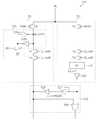
도 5는 도 3에 도시된 라이트 드라이버/센스 엠프 회로(550)의 구성도를 나타낸다. 도 5에 도시된 라이트 드라이버/센스 엠프 회로(550) 특히 NOR형 플래시 메모리 장치에 포함되는 회로들이나 본 발명의 범위가 이에 한정되는 것은 아니다. 도 5를 참조하면, 상기 라이트 드라이버/센스 엠프 회로(550)는 센스 엠프 회 로(551), 라이트 드라이버 회로(554), 및 검증 블락(556)을 포함한다.Fig. 5 shows a configuration diagram of the write driver /
상기 센스 엠프 회로(551)는 리드 명령(READ)에 응답하여 비트 라인(BL)을 통하여 메모리 셀 어레이(530)에 포함된 다수의 메모리 셀들 중에서 상응하는 메모리 셀로부터 제1 데이터를 센싱하여 출력할 수 있다.The
상기 센스 엠프 회로(551)는 센스 엠프(552) 및 적어도 하나의 스위칭 소자(Tr1, Tr2, 및 Tr3), 및 인버터(553)를 포함할 수 있다. 상기 센스 엠프(552)는 상기 상응하는 메모리 셀에 저장된 상기 제1 데이터를 센싱할 수 있다. 상기 적어도 하나의 스위칭 소자(Tr1, Tr2, 및 Tr3)는 상기 제1 데이터를 선택적으로 출력할 수 있다.The
상기 제1 데이터를 선택적으로 출력하기 위해서는 하나의 스위칭 소자(Tr1)만으로 충분하다. 그러나 데이터 출력을 위한 인코딩 양을 줄이기 위하여 상기 센스 엠프 회로(551)는 다수의 스위칭 소자들(Tr2 및 Tr3)을 더 포함할 수 있다. 상기 다수의 스위칭 소자들 각각은 리드 명령(READ)에 응답하여 게이팅되는 제1 트랜지스터(Tr1), 제1 데이터 출력 신호(D_outA)에 응답하여 게이팅되는 제2 트랜지스터(Tr2), 제2 데이터 출력 신호(D_outB)에 응답하여 게이팅되는 제3 트랜지스터(Tr3)로 구현될 수 있다.In order to selectively output the first data, only one switching element Tr1 is sufficient. However, in order to reduce the amount of encoding for data output, the
상기 리드 명령(READ), 상기 제1 데이터 출력 신호(D_outA), 및 상기 제2 데이터 출력 신호(D_outB)는 동일한 활성화 구간을 가질 수 있다. 상기 제1 데이터 출력 신호(D_outA) 및 상기 제2 데이터 출력 신호(D_outB)는 메모리 컨트롤러(510) 또는 칩 컨트롤러(560)로부터 수신되는 신호일 수 있다.The read command READ, the first data output signal D_outA, and the second data output signal D_outB may have the same activation period. The first data output signal D_outA and the second data output signal D_outB may be signals received from the
상기 메모리 셀이 프로그램된 경우에 상기 센스 엠프(552)로부터 출력되는 제1 데이터의 논리 값은 '0'이며, 그렇지 않은 경우에는 상기 제1 데이터의 논리 값은 '1'일 수 있다. 상기 인버터(553)는 상기 센스 엠프(552)로부터 출력되는 제1 데이터의 논리 값을 반전시켜 출력할 수 있다.When the memory cell is programmed, the logical value of the first data output from the
상기 라이트 드라이버 회로(554)는 프로그램 명령(PGM)에 응답하여 상기 메모리 셀 어레이(530)에 포함된 메모리 셀을 프로그램할 수 있으며, 상기 메모리 셀의 프로그램 여부를 나타내는 제2 데이터를 저장할 수 있다.The
상기 라이트 드라이버 회로(554)는 라이트 버퍼(555), 프로그램 명령(PGM)에 응답하여 게이팅되는 스위칭 소자(Tr4), 및 상기 검증 블락(556)으로부터 출력되는 제1 데이터를 선택적으로 상기 라이트 버퍼(555)로 전달하기 위한 적어도 하나의 스위칭 소자(Tr5 및 Tr6)를 포함할 수 있다.The
상기 라이트 버퍼(555)는 상기 메모리 셀의 프로그램 여부를 나타내는 제2 데이터(W_DATA)를 저장할 수 있다. 예컨대, 상기 메모리 셀에 대한 프로그램 동작이 수행된 경우에 상기 라이트 버퍼(555)에 저장되는 제2 데이터는 논리 값 '0'이며, 상기 메모리 셀에 대한 프로그램 여부 검증이 완료된 경우에 상기 라이트 버퍼(555)에 저장되는 제2 데이터는 논리 값 '1'일 수 있다.The
상기 라이트 버퍼(555)는 역방향으로 병렬 접속된 한 쌍의 인버터들(555a 및 555b)를 포함할 수 있다. 상기 라이트 버퍼(555)는 리셋 신호(RST)에 응답하여 상기 라이트 버퍼(555)를 리셋시키기 위한 트랜지스터(Tr7)를 더 포함할 수 있다.The
상기 검증 블락(556)으로부터 출력되는 제1 데이터를 선택적으로 출력하기 위해서는 하나의 스위칭 소자(Tr4 또는 Tr5)만으로 충분하나 인코딩 양을 줄이기 위하여 상기 라이트 드라이버 회로(554)는 다수의 스위칭 소자들(Tr4 및 Tr5)을 포함할 수 있다. 상기 제1 데이터 로드 신호(D_loadA) 및 상기 제2 데이터 로드 신호(D_loadB)는 메모리의 컨트롤러(510) 또는 칩 컨트롤러(560)으로부터 수신되는 신호일 수 있다. 상기 제1 데이터 로드 신호(D_loadA) 및 상기 제2 데이터 로드 신호(D_loadB)는 동일한 활성화 구간을 가질 수 있다.In order to selectively output the first data output from the
상기 다수의 스위칭 소자들(Tr4 및 Tr5) 각각은 제1 데이터 로드 신호(D_loadA)에 응답하여 게이팅되는 제4 트랜지스터(Tr4), 제2 데이터 로드 신호(D_outB)에 응답하여 게이팅되는 제5 트랜지스터(Tr5)로 구현될 수 있다. 상기 스위칭 소자(Tr6)는 상기 프로그램 명령(PGM)에 응답하여 메모리 셀에 대한 프로그램 동작 수행 시에는 단락되며 메모리 셀에 대한 프로그램 동작이 완료되면 개방된다.Each of the plurality of switching elements Tr4 and Tr5 includes a fourth transistor Tr4 gated in response to a first data load signal D_loadA and a fifth transistor Tr4 gated in response to a second data load signal D_outB. Tr5). The switching element Tr6 is short-circuited when the program operation for the memory cell is performed in response to the program command PGM, and is released when the program operation for the memory cell is completed.
상기 검증 블락(556)은 제1 리드 명령에 응답하여 상기 센스 엠프(552)로부터 출력되는 제1 데이터 및 상기 라이트 버퍼(555)에 저장된 상기 제2 데이터 사이의 비교 결과를 출력할 수 있다. 또한, 상기 검증 블락(226)은 상기 제1 리드 명령에 연속되는 제2 리드 명령에 응답하여 판단되는 상기 메모리 셀의 프로그램 여부에 기초하여 상기 제2 데이터를 업데이트할 수 있다.The
상기 검증 블락(556)은 비교 블락(559) 및 제어 블락(557 및 558)를 포함할 수 있다. 상기 비교 블락(559)은 상기 제1 데이터와 상기 제2 데이터의 비교 결과를 메모리 컨트롤러(510) 또는 칩 컨틀로러(560)로 출력할 수 있다.The
상기 비교 블락(559)은 상기 제1 데이터 및 제2 데이터에 대한 논리 합을 수행하는 논리 게이트(예컨대, OR 게이트)로 구현될 수 있다. 그러면 메모리 컨트롤러(510) 또는 칩 컨트롤러(560)는 상기 제1 데이터와 제2 데이터의 비교 결과에 기초하여 메모리 셀에 대한 프로그램 여부를 판단할 수 있다.The
예를 들면, 상기 메모리 셀이 프로그램된 경우 상기 센스 엠프(552)는 리드 명령에 논리 값 '0'을 갖는 제1 데이터를 출력하며 상기 인버터(553)는 논리 값 '1'을 갖는 제1 데이터를 출력한다. 라이트 버퍼(555)에는 논리 값 '0'을 갖는 제2 데이터를 저장되어 있다. 상기 비교 블락(559)은 상기 제1 데이터 및 제2 데이터에 대한 논리 합 결과인 논리 값 '1'을 출력할 수 있으며, 상기 메모리 셀은 프로그램된 것으로 판단될 수 있다.For example, when the memory cell is programmed, the
그러나, 상기 메모리 셀이 프로그램되지 않은 경우 상기 센스 엠프(552)는 리드 명령에 논리 값 '1'을 갖는 제1 데이터를 출력하며 상기 인버터(553)는 논리 값 '0'을 갖는 제1 데이터를 출력한다. 라이트 버퍼(555)에는 논리 값 '0'을 갖는 제2 데이터를 저장하고 있다. 상기 비교 블락(559)은 상기 제1 데이터 및 제2 데이터에 대한 논리 곱 결과인 논리 값 '0'을 출력할 수 있으며, 상기 메모리 셀은 프로그램되지 않은 것으로 판단될 수 있다.However, if the memory cell is not programmed, the
상기 제어 블락(557 및 558)은 상기 제1 데이터의 논리 값 및 제어 신호(UPDATE)에 기초하여 상기 제1 데이터를 선택적으로 상기 라이트 버퍼(555)로 출력할 수 있다. 상기 제어 블락(557 및 558)은 상기 제1 데이터의 논리 값이 제1 논리 값이고 상기 제어 신호가 활성화되면 상기 제1 데이터를 상기 라이트 버퍼(555)로 출력하고 상기 제2 데이터의 논리 값이 제2 논리 값이면 상기 제1 데이터가 상기 라이트 버퍼(555)로 출력되는 것을 차단할 수 있다.The control blocks 557 and 558 may selectively output the first data to the
상기 제어 블락(557 및 558)은 제1 제어 블락(557) 및 제2 제어 블락(558)를 포함할 수 있다. 상기 제1 제어 블락(557)은 상기 제1 데이터의 논리 값에 기초하여 상기 제1 데이터를 선택적으로 출력할 수 있다. 상기 제2 제어 블락(558)은 상기 제어 신호(UPDATE)에 응답하여 상기 제1 제어 블락(557)으로부터 출력되는 제1 데이터를 선택적으로 상기 라이트 버퍼(555)로 출력할 수 있다.The control blocks 557 and 558 may include a
상기 제1 제어 블락(557) 및 제2 제어 블락(558) 각각은 상기 제1 데이터의 논리 값 및 상기 제어 신호(UPDATE)에 응답하여 구동되는 제1 버퍼 및 제2 버퍼를 이용하여 구현될 수 있다. 도 5에 도시된 바와 같이, 상기 제1 버퍼(557) 및 제2 버퍼(558) 각각은 3상태 버퍼(tristate buffer)로 구현될 수 있다.Each of the
또한 상기 제1 제어 블락(557) 및 제2 제어 블락(558) 각각은 상기 제1 데이터의 논리 값 및 상기 제어 신호(UPDATE)에 응답하여 스위칭되는 상기 제3 스위칭 소자 및 제4 스위칭 소자를 이용하여 구현될 수 있음은 본 발명이 속하는 기술분야서 통상의 지식을 가진 자에게 자명한 것이라 할 것이다.Each of the
예를 들면, 상기 메모리 셀이 프로그램된 경우 센스 엠프 회로(551)의 인버터(553)는 논리 값 '1'을 갖는 제1 데이터를 출력한다. 그러면 제1 제어 블락(557)은 상기 제1 데이터를 버퍼링하고 상기 제2 제어 블락(558)은 제어 신호(UPDATE)가 활성화되는 구간에서 상기 제1 데이터를 버퍼링한다.For example, when the memory cell is programmed, the
그러나 상기 메모리 셀이 프로그램되지 않은 경우 센스 엠프 회로(551)의 인 버터(553)는 논리 값 '1'을 갖는 제1 데이터를 출력한다. 그러면 제1 제어 블락(557)은 상기 제1 데이터가 상기 제2 제어 블락(558)로 출력되는 것을 차단한다.However, if the memory cell is not programmed, the
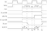
검증 동작이 수행되는 경우에 상기 리드 명령의 활성화 구간, 상기 적어도 하나의 제1 스위칭 소자(Tr1, Tr2, 및 Tr3)의 단락 구간, 및 상기 적어도 하나의 제2 스위칭 소자(Tr4 및 Tr5)의 단락 구간은 서로 동일할 수 있으며, 상기 제어 신호(UPDATE)의 활성화 구간은 제2 리드 명령의 활성화 구간 내에 포함될 수 있다. 상기 비휘발성 메모리 장치(500)에 대한 검증 동작은 도 6을 참조하여 좀더 구체적으로 살펴본다.(Tr1, Tr2, and Tr3) and the short-circuit period of the at least one second switching device (Tr4 and Tr5) when the verify operation is performed, And the activation period of the control signal UPDATE may be included in the activation period of the second read command. The verification operation for the
도 6은 도 5에 도시된 비휘발성 메모리 장치(520)에 대한 검증 동작을 설명하기 위한 타이임도이다. 도 6에 도시된 타이밍도는 메모리 셀에 대한 프로그램이 정상적으로 수행된 경우를 가정한 타이밍도이다. 이하 도1 내지 도 6를 참조하여 그 동작 과정을 살펴본다.FIG. 6 is a timing diagram for explaining the verify operation for the
상기 비휘발성 메모리 장치(520)는 클락 신호(CLK)에 기초하여 동작된다. 상기 비휘발성 메모리 장치(520)는 검증 신호(Verify)에 응답하여 검증 동작을 개시한다. 리드 명령(READ) 및 데이터 출력 신호들(D_outA/B)가 활성화되면 센스 엠프 회로(551)은 메모리 셀로부터 센싱된 제1 데이터를 출력한다.The
상기 리드 명령(READ)은 비교 구간(Compare)과 업데이트 구간(Update)으로 나누어질 수 있다. T1에서 T3까지의 비교 구간(Compare)에 상응하는 리드 명령의 구간을 제1 리드 명령이라 하고 T3에서 T5까지의 업데이트 구간(Update)에 상응하는 리드 명령의 구간을 제2 리드 명령이라 한다. 도 6을 참조하면, 상기 제1 리드 명령과 상기 제2 리드 명령은 서로 연속적으로 인가됨을 알 수 있다. 그러나 상기 제2 리드 명령은 상기 비휘발성 메모리 장치(520)의 특성 및 동작 환경에 따라 상기 제1 리드 명령과 미리 정해진 간격으로 인가될 수 있다.The read command (READ) can be divided into a comparison section (Compare) and an update section (Update). The interval of the read command corresponding to the comparison interval (Compare) from T1 to T3 is referred to as a first read command and the interval of the read command corresponding to the update interval (Update) from T3 to T5 is referred to as a second read command. Referring to FIG. 6, it can be seen that the first read command and the second read command are sequentially applied to each other. However, the second read command may be applied at a predetermined interval to the first read command according to the characteristics and operating environment of the
T1 시점에서 제1 리드 명령(READ) 및 데이터 출력 신호(D_outA/B)가 활성화 되면 센스 엠프(552)로부터 출력되는 제1 데이터는 소정의 지연 시간(D1)이 경과한 다음 논리 값 '0'으로 천이되며, 인버터(553)에 의하여 반전된 제1 데이터는 T2 시점 이후에는 논리 값 '1'이 된다. 여기서, 상기 센스 엠프(552)는 인밸리드(invalid) 값으로 논리 값 '1'을 갖는 제1 데이터를 출력하는 것으로 가정한다. 또한, T1 시점에서는 데이터 로드 신호(D_loadA/B)가 활성화되어 라이트 버퍼(555)로부터는 논리 값 '0'을 갖는 제2 데이터(W_DATA)가 출력된다.When the first read command READ and the data output signal D_outA / B are activated at the time T1, the first data output from the
그러므로 비교 회로(559)는 T2에서 T3 구간에서 논리 값 '1'을 갖는 제1 데이터 및 논리 값 '0'을 갖는 제2 데이터(W_DATA)에 대한 논리 합 결과인 논리 값 '1'을 출력한다. 그러면 메모리 컨트롤러(510) 또는 칩 컨트롤러(560)는 상기 메모리 셀이 프로그램된 것으로 판단할 수 있다.Therefore, the
활성화된 제2 리드 명령이 인가되는 T3 시점 이후 T4 시점에서 제어 신호(UPDATE) 신호가 활성화되면 제어 블락(557 및 558)는 논리 값 '1'을 갖는 제1 데이터를 상기 라이트 버퍼(555)로 출력한다. 그러면 상기 라이트 버퍼(555)는 소정의 지연 시간(D2)이 경과한 T5 시점부터 논리 값 '1'로 천이되며, T6 시점에서 검증 동작은 완료된다. 즉, 정상적으로 프로그램된 메모리 셀의 경우 상기 라이트 버퍼(555)에 저장된 제2 데이터(W_DATA)가 논리 값 '0'에서 논리 값 '1'로 업데이트되어 상기 메모리 셀에 대한 프로그램 동작은 불필요하며 상기 메모리 셀에 대한 검증 동작이 완료됨을 알 수 있다.When a control signal UPDATE signal is activated at a time point T4 after the time point T3 when the activated second read command is applied, the control blocks 557 and 558 transmit the first data having the logical value '1' to the
그러나 상기 메모리 셀이 정상적으로 프로그램되지 않았다면, 상기 센스 엠프 회로(552)는 논리 값 '0'을 갖는 제1 데이터를 출력하며, 3상태 버퍼로 구현된 제1 제어 블락(557)은 디스에이블된다. 그러므로 상기 라이트 버퍼(555)에 저장된 제2 데이터(W_DATA)는 논리 값 '0'을 유지하며, 칩 컨트롤러(560)는 상기 메모리 셀이 정상적으로 프로그램되지 않았으므로 상기 메모리 셀에 대한 프로그램 동작이 다시 수행되도록 상기 비휘발성 메모리 장치(520)를 제어한다.However, if the memory cell is not normally programmed, the
도 7은 본 발명의 실시예에 따른 비휘발성 메모리 장치(520)의 동작을 설명하기 위한 순서도이다. 이하, 도 5 및 도 7을 참조하여 그 과정을 좀더 상세히 살펴본다.7 is a flowchart for explaining the operation of the
상기 비휘발성 메모리 장치(520)는 메모리 셀 어레이(530)에 포함된 다수의 메모리 셀들 중에서 상응하는 메모리 셀들의 워드 라인에 소정의 레벨을 갖는 스텝 전압을 인가한다(S30). 그러면 상기 비휘발성 메모리 장치(520)는 라이트 드라이버 회로(554)으로부터 수신되는 데이터에 기초하여 상기 상응하는 메모리 셀들을 프로그램한다(S32).The
다음으로 상기 비휘발성 메모리 장치(520)는 상기 상응하는 메모리 셀들이 정상적으로 프로그램되었는지 여부를 검증하며(S32), 상기 상응하는 메모리 셀들에 대한 검증이 모두 완료되었는지를 판단한다(S33). 상기 상응하는 메모리 셀들에 대한 검증이 모두 완료되지 않은 경우 상기 비휘발성 메모리 장치(520)는 상기 상응 하는 메모리 셀들 중에서 검증이 완료되지 않은 메모리 셀의 워드 라인에 인가되는 스텝 전압을 미리 정해진 단계로 증가시킨다(S34).Next, the
상기 스텝 전압의 증가 정도는 동작 환경에 따랄, 즉, 상기 비휘발성 메모리 장치(520)의 특성, 공정 변동, 및 주변 환경 등을 고려하여 정해질 수 있다. 상기 상응하는 메모리 셀 모두에 대한 검증이 완료될 때까지 스텝 전압이 증가 단계(S34), 메모리 셀들에 대한 프로그램 단계(S31), 및 메모리 셀들에 대한 검증 단계(S32)는 반복적으로 수행될 수 있다.The degree of increase in the step voltage may be determined in accordance with the operating environment, that is, considering characteristics of the
도 8은 도 7에 도시된 메모리 셀의 프로그램 여부 검증 방법을 설명하기 위한 순서도이다. 도 5, 도 6, 및 도 8를 참조하여 메모리 셀에 대한 프로그램 여부 검증 단계를 좀더 구체적으로 살펴본다.FIG. 8 is a flowchart illustrating a method of verifying whether the memory cell shown in FIG. 7 is programmed. Referring to FIGS. 5, 6, and 8, the step of verifying whether the memory cell is programmed will be described in more detail.
센스 엠프 회로(551)는 제1 리드 명령에 응답하여 메모리 셀로부터 제1 데이터를 센싱하여 출력하고 라이트 드라이버 회로(554)은 라이트 버퍼(555)에 저장된 제2 데이터를 출력한다(S40). 그러면 검증 블락(556)의 비교 블락(559)은 상기 제1 데이터와 제2 데이터에 대한 비교 결과를 출력하며(S41), 컨트롤러는 상기 비교 결과에 기초하여 상기 메모리 셀의 프로그램 여부를 판단할 수 있다.The
도 5 및 도 6를 참조하여 설명한 바와 같이, 상기 비교 결과가 논리 값 '1'이면 상기 메모리 셀은 정상적으로 프로그램되었으며, 상기 비교 결과가 논리 값 '0'이면 상기 메모리 셀은 정상적으로 프로그램되지 않은 것으로 판단될 수 있다.As described with reference to FIGS. 5 and 6, if the comparison result is a logical value '1', the memory cell is normally programmed, and if the comparison result is a logic value '0', the memory cell is judged not to be normally programmed .
상기 비휘발성 메모리 장치(520)는 제1 리드 명령에 연속하여 인가되는 제2 리드 명령에 응답하여 라이트 드라이버 회로(554)의 라이트 버퍼(555)의 업데이트 여부를 판단한다(S42 및 S43). 도 5 및 도 6를 참조하여 설명한 바와 같이, 센스 엠프 회로(551)으로부터 출력되는 제1 데이터의 논리 값이 '1'이면 상기 메모리 셀은 정상적으로 프로그램되었으므로 상기 라이트 버퍼(555)에 저장된 논리 값 '0'을 갖는 제2 데이터는 논리 값 '1'로 업데이트된다(S44).The
그러나 센스 엠프 회로(551)으로부터 출력되는 제1 데이터의 논리 값이 '0'이면 상기 메모리 셀은 정상적으로 프로그램되지 았았으므로 상기 라이트 버퍼(555)에 저장된 논리 값 '0'은 그대로 유지된다(S45). 그러므로 상기 비휘발성 메모리 장치(520)은 프로그램 여부 검증 단계에서 상기 메모리 셀에 대한 프로그램 동작을 다시 수행한다.However, if the logic value of the first data output from the
본 발명의 실시예에 따른 비휘발성 메모리 장치(520) 그리고/또는 메모리 컨트롤러(510)는 다양한 형태들의 패키지를 이용하여 실장될 수 있다. 예를 들면, 본 발명의 실시예에 따른 비휘발성 메모리 장치 그리고/또는 메모리 컨트롤러는 PoP(Package on Package), Ball grid arrays(BGAs), Chip scale packages(CSPs), Plastic Leaded Chip Carrier(PLCC), Plastic Dual In-Line Package(PDIP), Die in Waffle Pack, Die in Wafer Form, Chip On Board(COB), Ceramic Dual In-Line Package(CERDIP), Plastic Metric Quad Flat Pack(MQFP), Thin Quad Flatpack(TQFP), Small Outline(SOIC), Shrink Small Outline Package(SSOP), Thin Small Outline(TSOP), Thin Quad Flatpack(TQFP), System In Package(SIP), Multi Chip Package(MCP), Wafer-level Fabricated Package(WFP), Wafer-Level Processed Stack Package(WSP) 등과 같은 패키지들을 이용하여 실장될 수 있다.The
본 발명의 실시예에 따른 비휘발성 메모리 장치의 동작 방법은 또한 컴퓨터로 읽을 수 있는 기록매체에 컴퓨터가 읽을 수 있는 코드로서 구현될 수 있다. 컴퓨터가 읽을 수 있는 기록매체는 컴퓨터 시스템에 의하여 읽혀질 수 있는 데이터가 저장되는 모든 종류의 기록장치를 포함한다.A method of operating a non-volatile memory device according to an embodiment of the present invention may also be implemented as computer readable code on a computer readable recording medium. A computer-readable recording medium includes all kinds of recording apparatuses in which data that can be read by a computer system is stored.
예컨대, 컴퓨터가 읽을 수 있는 기록매체에는 ROM, RAM, CD-ROM, 자기 테이프, 플로피 디스크, 광 데이터 저장장치 등이 있으며, 또한 본 발명의 실시예에 따른 비휘발성 메모리 장치의 동작 방법을 수행하기 위한 프로그램 코드는 캐리어 웨이브(예를 들어, 인터넷을 통한 전송)의 형태로 전송될 수도 있다.For example, the computer-readable recording medium includes a ROM, a RAM, a CD-ROM, a magnetic tape, a floppy disk, an optical data storage device, and the like. May be transmitted in the form of a carrier wave (e.g., transmission over the Internet).
또한 컴퓨터가 읽을 수 있는 기록매체는 네트워크로 연결된 컴퓨터 시스템에 분산되어, 분산방식으로 컴퓨터가 읽을 수 있는 코드가 저장되고 실행될 수 있다. 그리고 본 발명의 실시예에 따른 비휘발성 메모리 장치의 동작 방법을 구현하기 위한 기능적인 (functional) 프로그램, 코드 및 코드 세그먼트들은 본 발명이 속하는 기술분야의 프로그래머들에 의해 용이하게 추론될 수 있다.The computer readable recording medium may also be distributed over a networked computer system so that computer readable code can be stored and executed in a distributed manner. And functional programs, codes, and code segments for implementing a method of operating a non-volatile memory device according to an embodiment of the present invention can be easily deduced by programmers in the technical field to which the present invention belongs.
발명은 도면에 도시된 일 실시 예를 참고로 설명되었으나 이는 예시적인 것에 불과하며, 본 기술 분야의 통상의 지식을 가진 자라면 이로부터 다양한 변형 및 균등한 타 실시 예가 가능하다는 점을 이해할 것이다. 따라서, 본 발명의 진정한 기술적 보호 범위는 첨부된 등록청구범위의 기술적 사상에 의해 정해져야 할 것이다.While the present invention has been described with reference to exemplary embodiments thereof, it will be understood by those of ordinary skill in the art that various changes in form and details may be made therein without departing from the scope of the present invention. Accordingly, the true scope of the present invention should be determined by the technical idea of the appended claims.
도 1은 본 발명의 일 실시예에 따른 전자 시스템의 블락도를 나타낸다.1 shows a block diagram of an electronic system according to an embodiment of the present invention.
도 2는 도 1에 도시된 전자 시스템에 포함될 수 있는 본 발명의 다른 실시예에 따른 비휘발성 메모리 시스템의 블락도를 나타낸다.2 shows a block diagram of a non-volatile memory system according to another embodiment of the present invention that may be included in the electronic system shown in FIG.
도 3은 본 발명의 일 실시예에 따른 비휘발성 메모리 시스템의 블록도이다.3 is a block diagram of a non-volatile memory system in accordance with one embodiment of the present invention.
도 4는 본 발명의 일 실시예에 따른 비휘발성 메모리 장치의 블록도이다.4 is a block diagram of a non-volatile memory device in accordance with one embodiment of the present invention.
도 5는 도 3에 도시된 라이트 드라이버/센스 엠프 회로의 구성도이다.5 is a configuration diagram of the write driver / sense amplifier circuit shown in FIG.
도 6은 도 5에 도시된 비휘발성 메모리 장치의 동작을 설명하기 위한 타이밍도이다.6 is a timing chart for explaining the operation of the nonvolatile memory device shown in FIG.
도 7은 본 발명의 실시예에 따른 비휘발성 메모리 장치의 동작을 설명하기 위한 순서도이다.7 is a flowchart for explaining the operation of the nonvolatile memory device according to the embodiment of the present invention.
도 8은 도 7에 도시된 메모리 셀의 프로그램 여부 검증 단계를 설명하기 위한 순서도이다.8 is a flow chart for explaining the program verify step of the memory cell shown in FIG.
Claims (10)
Translated fromKoreanPriority Applications (2)
| Application Number | Priority Date | Filing Date | Title |
|---|---|---|---|
| KR1020080115151AKR101541812B1 (en) | 2008-11-19 | 2008-11-19 | Nonvolatile memory device |
| US12/619,227US8189393B2 (en) | 2008-11-19 | 2009-11-16 | Nonvolatile memory device with incremental step pulse programming |
Applications Claiming Priority (1)
| Application Number | Priority Date | Filing Date | Title |
|---|---|---|---|
| KR1020080115151AKR101541812B1 (en) | 2008-11-19 | 2008-11-19 | Nonvolatile memory device |
Publications (2)
| Publication Number | Publication Date |
|---|---|
| KR20100056132A KR20100056132A (en) | 2010-05-27 |
| KR101541812B1true KR101541812B1 (en) | 2015-08-06 |
Family
ID=42171977
Family Applications (1)
| Application Number | Title | Priority Date | Filing Date |
|---|---|---|---|
| KR1020080115151AExpired - Fee RelatedKR101541812B1 (en) | 2008-11-19 | 2008-11-19 | Nonvolatile memory device |
Country Status (2)
| Country | Link |
|---|---|
| US (1) | US8189393B2 (en) |
| KR (1) | KR101541812B1 (en) |
Families Citing this family (21)
| Publication number | Priority date | Publication date | Assignee | Title |
|---|---|---|---|---|
| US8019938B2 (en) | 2006-12-06 | 2011-09-13 | Fusion-I0, Inc. | Apparatus, system, and method for solid-state storage as cache for high-capacity, non-volatile storage |
| US8266503B2 (en) | 2009-03-13 | 2012-09-11 | Fusion-Io | Apparatus, system, and method for using multi-level cell storage in a single-level cell mode |
| US9223514B2 (en) | 2009-09-09 | 2015-12-29 | SanDisk Technologies, Inc. | Erase suspend/resume for memory |
| US8661184B2 (en) | 2010-01-27 | 2014-02-25 | Fusion-Io, Inc. | Managing non-volatile media |
| US8380915B2 (en) | 2010-01-27 | 2013-02-19 | Fusion-Io, Inc. | Apparatus, system, and method for managing solid-state storage media |
| US8854882B2 (en) | 2010-01-27 | 2014-10-07 | Intelligent Intellectual Property Holdings 2 Llc | Configuring storage cells |
| US9245653B2 (en) | 2010-03-15 | 2016-01-26 | Intelligent Intellectual Property Holdings 2 Llc | Reduced level cell mode for non-volatile memory |
| US8984216B2 (en) | 2010-09-09 | 2015-03-17 | Fusion-Io, Llc | Apparatus, system, and method for managing lifetime of a storage device |
| US10817502B2 (en) | 2010-12-13 | 2020-10-27 | Sandisk Technologies Llc | Persistent memory management |
| US9047178B2 (en) | 2010-12-13 | 2015-06-02 | SanDisk Technologies, Inc. | Auto-commit memory synchronization |
| US9218278B2 (en) | 2010-12-13 | 2015-12-22 | SanDisk Technologies, Inc. | Auto-commit memory |
| US10817421B2 (en) | 2010-12-13 | 2020-10-27 | Sandisk Technologies Llc | Persistent data structures |
| CN103262054B (en) | 2010-12-13 | 2015-11-25 | 桑迪士克科技股份有限公司 | For automatically submitting device, the system and method for storer to |
| US9208071B2 (en) | 2010-12-13 | 2015-12-08 | SanDisk Technologies, Inc. | Apparatus, system, and method for accessing memory |
| EP2549482B1 (en)* | 2011-07-22 | 2018-05-23 | SanDisk Technologies LLC | Apparatus, system and method for determining a configuration parameter for solid-state storage media |
| US9007843B2 (en)* | 2011-12-02 | 2015-04-14 | Cypress Semiconductor Corporation | Internal data compare for memory verification |
| US8605507B2 (en) | 2012-01-12 | 2013-12-10 | Macronix International Co., Ltd. | Flash programming technology for improved margin and inhibiting disturbance |
| EP2796493A1 (en)* | 2013-04-25 | 2014-10-29 | Huntsman International Llc | Composition comprising silylated polymers and polyhedral oligomeric metallo silsesquioxane |
| US9852799B2 (en) | 2014-11-19 | 2017-12-26 | Sandisk Technologies Llc | Configuration parameter management for non-volatile data storage |
| US9715918B1 (en) | 2016-05-23 | 2017-07-25 | Micron Technology, Inc. | Power reduction for a sensing operation of a memory cell |
| JP2019204565A (en)* | 2018-05-22 | 2019-11-28 | 東芝メモリ株式会社 | Semiconductor memory device and memory system |
Family Cites Families (9)
| Publication number | Priority date | Publication date | Assignee | Title |
|---|---|---|---|---|
| US5357462A (en) | 1991-09-24 | 1994-10-18 | Kabushiki Kaisha Toshiba | Electrically erasable and programmable non-volatile semiconductor memory with automatic write-verify controller |
| JP3142335B2 (en) | 1991-09-24 | 2001-03-07 | 株式会社東芝 | Nonvolatile semiconductor memory device |
| KR950003348A (en) | 1993-07-26 | 1995-02-16 | 최근선 | Method for producing polybutylene terephthalate |
| KR0169267B1 (en) | 1993-09-21 | 1999-02-01 | 사토 후미오 | Nonvolatile Semiconductor Memory |
| JP3226677B2 (en) | 1993-09-21 | 2001-11-05 | 株式会社東芝 | Nonvolatile semiconductor memory device |
| US6031760A (en)* | 1997-07-29 | 2000-02-29 | Kabushiki Kaisha Toshiba | Semiconductor memory device and method of programming the same |
| KR100672984B1 (en)* | 2004-12-14 | 2007-01-24 | 삼성전자주식회사 | Flash memory device can reduce program time |
| KR100706245B1 (en) | 2005-04-13 | 2007-04-11 | 삼성전자주식회사 | NOR flash memory device and its program method using bit scan method |
| KR100683856B1 (en)* | 2006-01-12 | 2007-02-15 | 삼성전자주식회사 | Programming method of flash memory to compensate for reduction of read margin due to high temperature stress |
- 2008
- 2008-11-19KRKR1020080115151Apatent/KR101541812B1/ennot_activeExpired - Fee Related
- 2009
- 2009-11-16USUS12/619,227patent/US8189393B2/ennot_activeExpired - Fee Related
Also Published As
| Publication number | Publication date |
|---|---|
| US8189393B2 (en) | 2012-05-29 |
| KR20100056132A (en) | 2010-05-27 |
| US20100124123A1 (en) | 2010-05-20 |
Similar Documents
| Publication | Publication Date | Title |
|---|---|---|
| KR101541812B1 (en) | Nonvolatile memory device | |
| US10665308B2 (en) | Semiconductor memory device | |
| US8625376B2 (en) | Semiconductor memory device and method of operation the same | |
| US7558114B2 (en) | Flash memory device capable of improving reliability | |
| KR102248835B1 (en) | Nonvolatile memory device and operating method thereof | |
| US8050101B2 (en) | Nonvolatile memory devices having erased-state verify capability and methods of operating same | |
| US9245646B2 (en) | Program verify operation in a memory device | |
| US8605512B2 (en) | Nonvolatile semiconductor memory device and method of operating a nonvolatile memory device | |
| KR101984796B1 (en) | Semiconductor memory device, memory system including the same and operating method thereof | |
| CN106157999A (en) | Semiconductor storage unit and operational approach thereof including illusory memory element | |
| KR20180027276A (en) | Semiconductor memory device and method for operating the same | |
| JP5336053B2 (en) | Nonvolatile memory device and method of operating the same | |
| KR101678888B1 (en) | Read method of data in non-volatile memory device | |
| CN101174456B (en) | Nonvolatile memory device and method of reading information from the same | |
| JP4931404B2 (en) | Nonvolatile memory device | |
| US7782676B2 (en) | Method of operating a nonvolatile memory device | |
| US7826276B2 (en) | Non-volatile memory device reducing data programming and verification time, and method of driving the same | |
| JP2010218623A (en) | Nonvolatile semiconductor storage device | |
| KR100732633B1 (en) | Flash memory device for discontinuous bit line decoding | |
| CN114863980B (en) | Semiconductor device and continuous readout method | |
| JP2007035163A (en) | Nonvolatile semiconductor memory device and signal processing system | |
| KR100605107B1 (en) | Flash memory device and its reading method | |
| CN118230792A (en) | Memory device and operation method thereof |
Legal Events
| Date | Code | Title | Description |
|---|---|---|---|
| PA0109 | Patent application | St.27 status event code:A-0-1-A10-A12-nap-PA0109 | |
| PG1501 | Laying open of application | St.27 status event code:A-1-1-Q10-Q12-nap-PG1501 | |
| R18-X000 | Changes to party contact information recorded | St.27 status event code:A-3-3-R10-R18-oth-X000 | |
| A201 | Request for examination | ||
| P11-X000 | Amendment of application requested | St.27 status event code:A-2-2-P10-P11-nap-X000 | |
| P13-X000 | Application amended | St.27 status event code:A-2-2-P10-P13-nap-X000 | |
| PA0201 | Request for examination | St.27 status event code:A-1-2-D10-D11-exm-PA0201 | |
| E902 | Notification of reason for refusal | ||
| PE0902 | Notice of grounds for rejection | St.27 status event code:A-1-2-D10-D21-exm-PE0902 | |
| E13-X000 | Pre-grant limitation requested | St.27 status event code:A-2-3-E10-E13-lim-X000 | |
| P11-X000 | Amendment of application requested | St.27 status event code:A-2-2-P10-P11-nap-X000 | |
| P13-X000 | Application amended | St.27 status event code:A-2-2-P10-P13-nap-X000 | |
| E701 | Decision to grant or registration of patent right | ||
| PE0701 | Decision of registration | St.27 status event code:A-1-2-D10-D22-exm-PE0701 | |
| PR0701 | Registration of establishment | St.27 status event code:A-2-4-F10-F11-exm-PR0701 | |
| PR1002 | Payment of registration fee | St.27 status event code:A-2-2-U10-U11-oth-PR1002 Fee payment year number:1 | |
| PG1601 | Publication of registration | St.27 status event code:A-4-4-Q10-Q13-nap-PG1601 | |
| FPAY | Annual fee payment | Payment date:20180629 Year of fee payment:4 | |
| PR1001 | Payment of annual fee | St.27 status event code:A-4-4-U10-U11-oth-PR1001 Fee payment year number:4 | |
| PR1001 | Payment of annual fee | St.27 status event code:A-4-4-U10-U11-oth-PR1001 Fee payment year number:5 | |
| PR1001 | Payment of annual fee | St.27 status event code:A-4-4-U10-U11-oth-PR1001 Fee payment year number:6 | |
| PR1001 | Payment of annual fee | St.27 status event code:A-4-4-U10-U11-oth-PR1001 Fee payment year number:7 | |
| PR1001 | Payment of annual fee | St.27 status event code:A-4-4-U10-U11-oth-PR1001 Fee payment year number:8 | |
| PC1903 | Unpaid annual fee | St.27 status event code:A-4-4-U10-U13-oth-PC1903 Not in force date:20230730 Payment event data comment text:Termination Category : DEFAULT_OF_REGISTRATION_FEE | |
| PC1903 | Unpaid annual fee | St.27 status event code:N-4-6-H10-H13-oth-PC1903 Ip right cessation event data comment text:Termination Category : DEFAULT_OF_REGISTRATION_FEE Not in force date:20230730 |