KR101539326B1 - Z-inversion Type Display Device and Manufacturing Method thereof - Google Patents
Z-inversion Type Display Device and Manufacturing Method thereofDownload PDFInfo
- Publication number
- KR101539326B1 KR101539326B1KR1020140052330AKR20140052330AKR101539326B1KR 101539326 B1KR101539326 B1KR 101539326B1KR 1020140052330 AKR1020140052330 AKR 1020140052330AKR 20140052330 AKR20140052330 AKR 20140052330AKR 101539326 B1KR101539326 B1KR 101539326B1
- Authority
- KR
- South Korea
- Prior art keywords
- drain electrode
- thin film
- film transistor
- electrode
- gate line
- Prior art date
- Legal status (The legal status is an assumption and is not a legal conclusion. Google has not performed a legal analysis and makes no representation as to the accuracy of the status listed.)
- Active
Links
Images


Classifications
- G—PHYSICS
- G02—OPTICS
- G02F—OPTICAL DEVICES OR ARRANGEMENTS FOR THE CONTROL OF LIGHT BY MODIFICATION OF THE OPTICAL PROPERTIES OF THE MEDIA OF THE ELEMENTS INVOLVED THEREIN; NON-LINEAR OPTICS; FREQUENCY-CHANGING OF LIGHT; OPTICAL LOGIC ELEMENTS; OPTICAL ANALOGUE/DIGITAL CONVERTERS
- G02F1/00—Devices or arrangements for the control of the intensity, colour, phase, polarisation or direction of light arriving from an independent light source, e.g. switching, gating or modulating; Non-linear optics
- G02F1/01—Devices or arrangements for the control of the intensity, colour, phase, polarisation or direction of light arriving from an independent light source, e.g. switching, gating or modulating; Non-linear optics for the control of the intensity, phase, polarisation or colour
- G02F1/13—Devices or arrangements for the control of the intensity, colour, phase, polarisation or direction of light arriving from an independent light source, e.g. switching, gating or modulating; Non-linear optics for the control of the intensity, phase, polarisation or colour based on liquid crystals, e.g. single liquid crystal display cells
- G02F1/133—Constructional arrangements; Operation of liquid crystal cells; Circuit arrangements
- G02F1/136—Liquid crystal cells structurally associated with a semi-conducting layer or substrate, e.g. cells forming part of an integrated circuit
- G02F1/1362—Active matrix addressed cells
- H—ELECTRICITY
- H10—SEMICONDUCTOR DEVICES; ELECTRIC SOLID-STATE DEVICES NOT OTHERWISE PROVIDED FOR
- H10D—INORGANIC ELECTRIC SEMICONDUCTOR DEVICES
- H10D86/00—Integrated devices formed in or on insulating or conducting substrates, e.g. formed in silicon-on-insulator [SOI] substrates or on stainless steel or glass substrates
- H10D86/40—Integrated devices formed in or on insulating or conducting substrates, e.g. formed in silicon-on-insulator [SOI] substrates or on stainless steel or glass substrates characterised by multiple TFTs
- H10D86/60—Integrated devices formed in or on insulating or conducting substrates, e.g. formed in silicon-on-insulator [SOI] substrates or on stainless steel or glass substrates characterised by multiple TFTs wherein the TFTs are in active matrices
- G—PHYSICS
- G02—OPTICS
- G02F—OPTICAL DEVICES OR ARRANGEMENTS FOR THE CONTROL OF LIGHT BY MODIFICATION OF THE OPTICAL PROPERTIES OF THE MEDIA OF THE ELEMENTS INVOLVED THEREIN; NON-LINEAR OPTICS; FREQUENCY-CHANGING OF LIGHT; OPTICAL LOGIC ELEMENTS; OPTICAL ANALOGUE/DIGITAL CONVERTERS
- G02F1/00—Devices or arrangements for the control of the intensity, colour, phase, polarisation or direction of light arriving from an independent light source, e.g. switching, gating or modulating; Non-linear optics
- G02F1/01—Devices or arrangements for the control of the intensity, colour, phase, polarisation or direction of light arriving from an independent light source, e.g. switching, gating or modulating; Non-linear optics for the control of the intensity, phase, polarisation or colour
- G02F1/13—Devices or arrangements for the control of the intensity, colour, phase, polarisation or direction of light arriving from an independent light source, e.g. switching, gating or modulating; Non-linear optics for the control of the intensity, phase, polarisation or colour based on liquid crystals, e.g. single liquid crystal display cells
- G02F1/133—Constructional arrangements; Operation of liquid crystal cells; Circuit arrangements
- G02F1/136—Liquid crystal cells structurally associated with a semi-conducting layer or substrate, e.g. cells forming part of an integrated circuit
- G02F1/1362—Active matrix addressed cells
- G02F1/136286—Wiring, e.g. gate line, drain line
- G—PHYSICS
- G02—OPTICS
- G02F—OPTICAL DEVICES OR ARRANGEMENTS FOR THE CONTROL OF LIGHT BY MODIFICATION OF THE OPTICAL PROPERTIES OF THE MEDIA OF THE ELEMENTS INVOLVED THEREIN; NON-LINEAR OPTICS; FREQUENCY-CHANGING OF LIGHT; OPTICAL LOGIC ELEMENTS; OPTICAL ANALOGUE/DIGITAL CONVERTERS
- G02F1/00—Devices or arrangements for the control of the intensity, colour, phase, polarisation or direction of light arriving from an independent light source, e.g. switching, gating or modulating; Non-linear optics
- G02F1/01—Devices or arrangements for the control of the intensity, colour, phase, polarisation or direction of light arriving from an independent light source, e.g. switching, gating or modulating; Non-linear optics for the control of the intensity, phase, polarisation or colour
- G02F1/13—Devices or arrangements for the control of the intensity, colour, phase, polarisation or direction of light arriving from an independent light source, e.g. switching, gating or modulating; Non-linear optics for the control of the intensity, phase, polarisation or colour based on liquid crystals, e.g. single liquid crystal display cells
- G02F1/133—Constructional arrangements; Operation of liquid crystal cells; Circuit arrangements
- G02F1/1333—Constructional arrangements; Manufacturing methods
- G02F1/133345—Insulating layers
- G—PHYSICS
- G02—OPTICS
- G02F—OPTICAL DEVICES OR ARRANGEMENTS FOR THE CONTROL OF LIGHT BY MODIFICATION OF THE OPTICAL PROPERTIES OF THE MEDIA OF THE ELEMENTS INVOLVED THEREIN; NON-LINEAR OPTICS; FREQUENCY-CHANGING OF LIGHT; OPTICAL LOGIC ELEMENTS; OPTICAL ANALOGUE/DIGITAL CONVERTERS
- G02F1/00—Devices or arrangements for the control of the intensity, colour, phase, polarisation or direction of light arriving from an independent light source, e.g. switching, gating or modulating; Non-linear optics
- G02F1/01—Devices or arrangements for the control of the intensity, colour, phase, polarisation or direction of light arriving from an independent light source, e.g. switching, gating or modulating; Non-linear optics for the control of the intensity, phase, polarisation or colour
- G02F1/13—Devices or arrangements for the control of the intensity, colour, phase, polarisation or direction of light arriving from an independent light source, e.g. switching, gating or modulating; Non-linear optics for the control of the intensity, phase, polarisation or colour based on liquid crystals, e.g. single liquid crystal display cells
- G02F1/133—Constructional arrangements; Operation of liquid crystal cells; Circuit arrangements
- G02F1/1333—Constructional arrangements; Manufacturing methods
- G02F1/1343—Electrodes
- G02F1/134309—Electrodes characterised by their geometrical arrangement
- G—PHYSICS
- G02—OPTICS
- G02F—OPTICAL DEVICES OR ARRANGEMENTS FOR THE CONTROL OF LIGHT BY MODIFICATION OF THE OPTICAL PROPERTIES OF THE MEDIA OF THE ELEMENTS INVOLVED THEREIN; NON-LINEAR OPTICS; FREQUENCY-CHANGING OF LIGHT; OPTICAL LOGIC ELEMENTS; OPTICAL ANALOGUE/DIGITAL CONVERTERS
- G02F1/00—Devices or arrangements for the control of the intensity, colour, phase, polarisation or direction of light arriving from an independent light source, e.g. switching, gating or modulating; Non-linear optics
- G02F1/01—Devices or arrangements for the control of the intensity, colour, phase, polarisation or direction of light arriving from an independent light source, e.g. switching, gating or modulating; Non-linear optics for the control of the intensity, phase, polarisation or colour
- G02F1/13—Devices or arrangements for the control of the intensity, colour, phase, polarisation or direction of light arriving from an independent light source, e.g. switching, gating or modulating; Non-linear optics for the control of the intensity, phase, polarisation or colour based on liquid crystals, e.g. single liquid crystal display cells
- G02F1/133—Constructional arrangements; Operation of liquid crystal cells; Circuit arrangements
- G02F1/1333—Constructional arrangements; Manufacturing methods
- G02F1/1343—Electrodes
- G02F1/13439—Electrodes characterised by their electrical, optical, physical properties; materials therefor; method of making
- G—PHYSICS
- G02—OPTICS
- G02F—OPTICAL DEVICES OR ARRANGEMENTS FOR THE CONTROL OF LIGHT BY MODIFICATION OF THE OPTICAL PROPERTIES OF THE MEDIA OF THE ELEMENTS INVOLVED THEREIN; NON-LINEAR OPTICS; FREQUENCY-CHANGING OF LIGHT; OPTICAL LOGIC ELEMENTS; OPTICAL ANALOGUE/DIGITAL CONVERTERS
- G02F1/00—Devices or arrangements for the control of the intensity, colour, phase, polarisation or direction of light arriving from an independent light source, e.g. switching, gating or modulating; Non-linear optics
- G02F1/01—Devices or arrangements for the control of the intensity, colour, phase, polarisation or direction of light arriving from an independent light source, e.g. switching, gating or modulating; Non-linear optics for the control of the intensity, phase, polarisation or colour
- G02F1/13—Devices or arrangements for the control of the intensity, colour, phase, polarisation or direction of light arriving from an independent light source, e.g. switching, gating or modulating; Non-linear optics for the control of the intensity, phase, polarisation or colour based on liquid crystals, e.g. single liquid crystal display cells
- G02F1/133—Constructional arrangements; Operation of liquid crystal cells; Circuit arrangements
- G02F1/136—Liquid crystal cells structurally associated with a semi-conducting layer or substrate, e.g. cells forming part of an integrated circuit
- G02F1/1362—Active matrix addressed cells
- G02F1/136227—Through-hole connection of the pixel electrode to the active element through an insulation layer
- G—PHYSICS
- G02—OPTICS
- G02F—OPTICAL DEVICES OR ARRANGEMENTS FOR THE CONTROL OF LIGHT BY MODIFICATION OF THE OPTICAL PROPERTIES OF THE MEDIA OF THE ELEMENTS INVOLVED THEREIN; NON-LINEAR OPTICS; FREQUENCY-CHANGING OF LIGHT; OPTICAL LOGIC ELEMENTS; OPTICAL ANALOGUE/DIGITAL CONVERTERS
- G02F1/00—Devices or arrangements for the control of the intensity, colour, phase, polarisation or direction of light arriving from an independent light source, e.g. switching, gating or modulating; Non-linear optics
- G02F1/01—Devices or arrangements for the control of the intensity, colour, phase, polarisation or direction of light arriving from an independent light source, e.g. switching, gating or modulating; Non-linear optics for the control of the intensity, phase, polarisation or colour
- G02F1/13—Devices or arrangements for the control of the intensity, colour, phase, polarisation or direction of light arriving from an independent light source, e.g. switching, gating or modulating; Non-linear optics for the control of the intensity, phase, polarisation or colour based on liquid crystals, e.g. single liquid crystal display cells
- G02F1/133—Constructional arrangements; Operation of liquid crystal cells; Circuit arrangements
- G02F1/136—Liquid crystal cells structurally associated with a semi-conducting layer or substrate, e.g. cells forming part of an integrated circuit
- G02F1/1362—Active matrix addressed cells
- G02F1/1368—Active matrix addressed cells in which the switching element is a three-electrode device
- H—ELECTRICITY
- H10—SEMICONDUCTOR DEVICES; ELECTRIC SOLID-STATE DEVICES NOT OTHERWISE PROVIDED FOR
- H10D—INORGANIC ELECTRIC SEMICONDUCTOR DEVICES
- H10D86/00—Integrated devices formed in or on insulating or conducting substrates, e.g. formed in silicon-on-insulator [SOI] substrates or on stainless steel or glass substrates
- H10D86/01—Manufacture or treatment
- H10D86/021—Manufacture or treatment of multiple TFTs
- H10D86/0212—Manufacture or treatment of multiple TFTs comprising manufacture, treatment or coating of substrates
- H—ELECTRICITY
- H10—SEMICONDUCTOR DEVICES; ELECTRIC SOLID-STATE DEVICES NOT OTHERWISE PROVIDED FOR
- H10D—INORGANIC ELECTRIC SEMICONDUCTOR DEVICES
- H10D86/00—Integrated devices formed in or on insulating or conducting substrates, e.g. formed in silicon-on-insulator [SOI] substrates or on stainless steel or glass substrates
- H10D86/40—Integrated devices formed in or on insulating or conducting substrates, e.g. formed in silicon-on-insulator [SOI] substrates or on stainless steel or glass substrates characterised by multiple TFTs
- H10D86/441—Interconnections, e.g. scanning lines
- H—ELECTRICITY
- H10—SEMICONDUCTOR DEVICES; ELECTRIC SOLID-STATE DEVICES NOT OTHERWISE PROVIDED FOR
- H10K—ORGANIC ELECTRIC SOLID-STATE DEVICES
- H10K59/00—Integrated devices, or assemblies of multiple devices, comprising at least one organic light-emitting element covered by group H10K50/00
- H10K59/10—OLED displays
- H10K59/12—Active-matrix OLED [AMOLED] displays
- H10K59/121—Active-matrix OLED [AMOLED] displays characterised by the geometry or disposition of pixel elements
- H10K59/1213—Active-matrix OLED [AMOLED] displays characterised by the geometry or disposition of pixel elements the pixel elements being TFTs
- G—PHYSICS
- G02—OPTICS
- G02F—OPTICAL DEVICES OR ARRANGEMENTS FOR THE CONTROL OF LIGHT BY MODIFICATION OF THE OPTICAL PROPERTIES OF THE MEDIA OF THE ELEMENTS INVOLVED THEREIN; NON-LINEAR OPTICS; FREQUENCY-CHANGING OF LIGHT; OPTICAL LOGIC ELEMENTS; OPTICAL ANALOGUE/DIGITAL CONVERTERS
- G02F2201/00—Constructional arrangements not provided for in groups G02F1/00 - G02F7/00
- G02F2201/12—Constructional arrangements not provided for in groups G02F1/00 - G02F7/00 electrode
- G02F2201/123—Constructional arrangements not provided for in groups G02F1/00 - G02F7/00 electrode pixel
- H—ELECTRICITY
- H10—SEMICONDUCTOR DEVICES; ELECTRIC SOLID-STATE DEVICES NOT OTHERWISE PROVIDED FOR
- H10K—ORGANIC ELECTRIC SOLID-STATE DEVICES
- H10K59/00—Integrated devices, or assemblies of multiple devices, comprising at least one organic light-emitting element covered by group H10K50/00
- H10K59/10—OLED displays
- H10K59/12—Active-matrix OLED [AMOLED] displays
- H10K59/1201—Manufacture or treatment
Landscapes
- Physics & Mathematics (AREA)
- Nonlinear Science (AREA)
- Mathematical Physics (AREA)
- Chemical & Material Sciences (AREA)
- Crystallography & Structural Chemistry (AREA)
- General Physics & Mathematics (AREA)
- Optics & Photonics (AREA)
- Engineering & Computer Science (AREA)
- Microelectronics & Electronic Packaging (AREA)
- Geometry (AREA)
- Liquid Crystal (AREA)
- Devices For Indicating Variable Information By Combining Individual Elements (AREA)
Abstract
Translated fromKoreanDescription
Translated fromKorean본 발명은 표시장치 및 그 제조방법에 관한 기술이다. 특히, 본 발명은 Z-인버전 방식으로 화소가 형성되는 표시장치 및 그 제조방법에 관한 기술이다.The present invention relates to a display device and a method of manufacturing the same. Particularly, the present invention relates to a display device in which pixels are formed in a Z-in version system and a manufacturing method thereof.
정보화 사회가 발전함에 따라 화상을 표시하기 위한 표시장치에 대한 요구가 다양한 형태로 증가하고 있으며, 근래에는 액정표시장치(LCD: Liquid Crystal Display), 플라즈마 표시장치(PDP: Plasma Display Panel), 유기전계발광 표시장치(OLED: Organic Light Emitting Diode Display Device)와 같은 여러 가지 표시장치가 활용되고 있다.2. Description of the Related Art [0002] As an information-oriented society develops, there have been various demands for display devices for displaying images. Recently, liquid crystal displays (LCDs), plasma display panels (PDPs) Various display devices such as an OLED (Organic Light Emitting Diode Display Device) have been utilized.
이러한 표시장치 중 액정 표시장치(LCD)는 화소영역 각각을 온(on)/오프(off) 제어하기 위한 스위칭 소자인 트랜지스터를 포함하는 어레이 기판과, 컬러필터 및/또는 블랙매트릭스 등을 구비한 상부기판과, 그 사이에 형성되는 액정물질층을 포함하는 표시패널과, 트랜지스터를 제어하기 위한 구동부를 포함하여 구성되며, 화소 영역에 구비된 화소(Pixel; P) 전극 및 공통 전압(Vcom) 전극 사이에 인가되는 전계에 따라 액정층의 배열 상태가 조절되고 그에 따라 광의 투과도가 조절되어 화상이 표시되는 장치이다.Among these display devices, a liquid crystal display (LCD) includes an array substrate including a transistor serving as a switching element for controlling on / off of each pixel region, an upper substrate having a color filter and / or a black matrix, A liquid crystal display device comprising a substrate, a display panel including a liquid crystal material layer formed therebetween, and a driver for controlling the transistor, the liquid crystal display device comprising: a pixel (P) electrode and a common voltage The arrangement of the liquid crystal layer is adjusted according to an electric field applied to the liquid crystal layer, and the transmittance of light is controlled thereby to display an image.
이러한 액정표시장치는 액정의 열화를 방지함과 아울러 표시 품질을 향상시키기 위하여, 액정패널을 인버전 방식으로 구동한다. 인버전 방식으로는 프레임 인버전 방식(Frame Inversion System), 라인 인버전 방식(Line Inversion System), 컬럼 인버전 방식(Column Inversion System) 또는 도트 인버전 방식(Dot Inversion System) 등이 이용되고 있다.Such a liquid crystal display device drives the liquid crystal panel in an inversion mode in order to prevent deterioration of liquid crystal and improve display quality. A frame inversion system, a line inversion system, a column inversion system, a dot inversion system, or the like is used as the in-version system.
인버전 구동방식들 중 프레임 인버전이나 라인 인버전 및 컬럼 인버전 방식들은 도트 인버전 방식에 비해 소비전력을 감소시킬 수는 있으나, 크로스토크(crosstalk) 현상이 발생하거나 상하 휘도 차가 발생하는 등의 화질 저하 문제가 있었다. 한편, 도트 인버전 방식의 경우엔 상기와 같은 화질 저하 문제를 줄일 수 있어 프레임 인버전이나 라인 인버전 및 컬럼 인버전 방식들에 비하여 더 뛰어난 화질의 화상을 제공할 수 있다. 하지만, 도트 인버전 방식은 라인 인버전 방식이나 컬럼 인버전 방식들에 비해 전력 소모가 너무 큰 문제가 있었다.Among the in-version driving methods, the frame-in version, the line-in version and the column-inversion method can reduce the power consumption as compared with the dot-in-version method, but the crosstalk phenomenon or the difference in the vertical luminance There was a problem of image quality deterioration. On the other hand, in the case of the dot inversion method, it is possible to reduce the image quality degradation problem as described above, and thus it is possible to provide an image of higher image quality than the frame inversion, line inversion, and column inversion methods. However, the dot inversion method has a problem that the power consumption is too high as compared with the line inversion method or the column inversion method.
전술한 방식들의 문제를 개선하기 위해 제시된 방식이 Z-인버전(Z-Inversion System) 방식이다. Z-인버전 방식은, 트랜지스터(TFT)와 화소전극(P)이 좌측과 우측으로 교번하며 배열되는 데이터 라인들에, 컬럼 인버전 방식으로 데이터 전압를 공급하는 방법이다. 즉, Z-인버전 방식은, 컬럼 인버전 방식의 개선된 구조로서, 회로구동방식은 컬럼 인버전 방식을 이용하고 있으나, 액정패널의 트랜지스터(TFT)의 방향을 각 라인(Line)마다 반대로 형성하여, 화면표시는 도트 인버전 방식(Dot inversion System)과 동일하게 구현하고 있다. 부연하여 설명하면, Z-인버전 방식은 화질적으로는 도트 인버전 방식과 유사한 효과를 가지면서도, 데이터(Data) 측면에서는 컬럼 인버전 방식을 이용한 것으로서, 화질적으로 우수할 뿐만 아니라, 소비전력을 절감시킬 수 있는 방법이다.In order to remedy the problems of the above-described schemes, the proposed scheme is a Z-Inversion System. The Z-inversion method is a method of supplying a data voltage in a column-wise manner to the data lines where the transistor (TFT) and the pixel electrode P are alternately arranged to the left and right. In other words, the Z-in version method is an improved structure of a column-type version method, and the circuit driving method uses a column type version method. However, since the direction of the TFT of the liquid crystal panel is reversed Thus, the screen display is implemented in the same manner as the dot inversion system. Described in detail, the Z-in version system has an effect similar to that of the dot inversion system in image quality, but also uses a version system in the column of data in terms of data, .
도 1은 Z-인버전 방식 표시장치의 화소에 위치하는 박막트랜지스터를 나타낸다.FIG. 1 shows a thin film transistor located in a pixel of a Z-inversion display device.
Z-인버전 방식의 표시장치에서 일부의 화소들(예를 들어, 홀수행에 위치하는 화소들)에 위치하는 박막트랜지스터는 채널이 왼쪽방향으로 형성되고, 다른 일부의 화소들(예를 들어, 짝수행에 위치하는 화소들)에 위치하는 박막트랜지스터는 채널이 오른쪽방향으로 형성된다.In a Z-inversion display device, a thin film transistor located in a part of pixels (for example, pixels positioned in a hole) has a channel formed in the left direction and a part of pixels (for example, The pixels located in the even-numbered rows) are formed in the right direction.
도 1의 (a)를 참조하면, 상측에 위치하는 박막트랜지스터는 채널이 왼쪽방향으로 형성되어 있고, 하측에 위치하는 박막트랜지스터는 채널이 오른쪽방향으로 형성되어 있다.Referring to FIG. 1 (a), the channel of the thin film transistor located on the upper side is formed in the left direction, and the channel of the thin film transistor located on the lower side is formed in the right direction.
채널이 왼쪽방향으로 형성되어 있기 위해서는 박막트랜지스터의 드레인 전극(화소 전극과 전기적으로 연결되어 있는 전극)이 소스 전극의 왼쪽방향에 위치해야 한다. 이와 반대로 채널이 오른쪽방향으로 형성되어 있기 위해서는 박막트랜지스터의 드레인 전극이 소스 전극의 오른쪽방향에 위치해야 한다.In order for the channel to be formed in the left direction, the drain electrode (the electrode electrically connected to the pixel electrode) of the thin film transistor should be located in the left direction of the source electrode. On the other hand, in order for the channel to be formed in the right direction, the drain electrode of the thin film transistor must be positioned to the right of the source electrode.
이렇게 Z-인버전 방식 표시장치에서는 박막트랜지스터의 드레인 전극이 위치하는 방향이 화소별로 상이하다. 구체적으로, 홀수행 화소에서의 드레인 전극이 위치하는 방향과 짝수행 화소에서의 드레인 전극이 위치하는 방향이 상이하다.In the Z-inversion display device, the direction in which the drain electrode of the thin film transistor is located differs for each pixel. Specifically, the direction in which the drain electrode is located in the hole-performing pixel differs from the direction in which the drain electrode is located in the even-performing pixel.
도 1의 (a)는 정상적인 경우의 드레인 전극 위치를 나타낸다.1 (a) shows the position of the drain electrode in a normal case.
도 1의 (a)를 참조하면, 채널이 왼쪽방향으로 형성되는 상측 박막트랜지스터에서의 드레인 전극(20a)과 게이트 전극(10a)이 오버랩되는 면적과 채널이 오른쪽방향으로 형성되는 하측 박막트랜지스터에서의 드레인 전극(20b)과 게이트 전극(10b)이 오버랩되는 면적이 실질적으로 동일하다.Referring to FIG. 1 (a), an area where the
박막트랜지스터의 드레인 전극과 게이트 전극이 오버랩(overlap)되는 면적은 캐패시턴스를 형성하는데, 이러한 캐패시턴스를 Cgs라고 한다. 이때, 오버랩되는 면적의 크기에 따라 Cgs의 크기가 결정되는데, 도 1의 (a)와 같이 정상적인 경우에는 전술한 두 박막트랜지스터의 Cgs의 크기가 동일하게 된다.An area where the drain electrode and the gate electrode of the thin film transistor overlap overlap each other to form a capacitance, and this capacitance is referred to as Cgs. At this time, the size of the Cgs is determined according to the size of the overlapped area. In the normal case as shown in FIG. 1A, the Cgs of the two thin film transistors described above are the same.
한편, 도 1의 (b)는 게이트 전극층과 소스/드레인 전극층이 2.5um 어긋나서 형성된 경우의 드레인 전극 위치를 나타낸다.On the other hand, FIG. 1 (b) shows the position of the drain electrode when the gate electrode layer and the source / drain electrode layer are formed to be shifted by 2.5 .mu.m.
게이트 전극층과 소스/드레인 전극층은 서로 다른 마스크를 사용하여 서로 다른 층에서 형성된다. 이때, 게이트 전극층을 형성하기 위한 마스크와 소스/드레인 전극층을 형성하기 위한 마스크의 기준 위치가 미세하게 어긋날 수 있는데, 예를 들어, 그 기준 위치가 2.5um 어긋날 수 있는데, 이렇게 어긋날 경우, 드레인 전극의 위치가 도 1의 (b)와 같이 형성될 수 있다.The gate electrode layer and the source / drain electrode layer are formed in different layers using different masks. At this time, the reference position of the mask for forming the gate electrode layer and the mask for forming the source / drain electrode layer may be slightly shifted. For example, the reference position may be displaced by 2.5 um. The position can be formed as shown in Fig. 1 (b).
도 1의 (b)를 참조하면, 채널이 왼쪽방향으로 형성되는 상측 박막트랜지스터에서의 드레인 전극(20c)과 게이트 전극(10c)이 오버랩되는 면적이 채널이 오른쪽방향으로 형성되는 하측 박막트랜지스터에서의 드레인 전극(20d)과 게이트 전극(10d)이 오버랩되는 면적보다 작다.Referring to FIG. 1B, an area where the
이렇게 드레인 전극과 게이트 전극이 오버랩되는 면적이 상이하면 각각의 박막트랜지스터에 형성되는 Cgs의 크기가 상이하게 된다. 도 1의 (b)의 경우, 상측 박막트랜지스터의 Cgs가 하측 박막트랜지스터의 Cgs 크기보다 작아지게 된다.If the area where the drain electrode and the gate electrode overlap each other is different, the size of Cgs formed in each thin film transistor becomes different. In the case of FIG. 1 (b), the Cgs of the upper thin film transistor becomes smaller than the Cgs of the lower thin film transistor.
Cgs는 게이트 오프(OFF) 시 발생하는 커플링 현상으로 인해 화소에 충전되어 있던 전압을 낮추는 기능을 하는데, 충전 전압을 낮추는 정도는 Cgs의 크기에 따라 다르게 결정된다. 이에 따라, 화소별로 Cgs의 크기가 다른 경우, Cgs가 각 화소에서 충전 전압을 낮추는 정도가 상이하게 되어 결국에는 각 화소의 충전 전압이 달라지게 된다.Cgs has a function of lowering the voltage charged in a pixel due to a coupling phenomenon occurring when the gate is turned off (OFF). The degree of lowering the charging voltage depends on the magnitude of Cgs. Accordingly, when the magnitude of Cgs is different for each pixel, the degree to which Cgs lowers the charging voltage in each pixel becomes different, and finally, the charging voltage of each pixel changes.
전술한 바와 같이 Z-인버전 방식 표시장치의 경우, 마스크의 어긋남 등의 이유로 게이트 전극층과 소스/드레인 전극층이 어긋날 수 있는데, 이때, 각 화소별로 Cgs의 크기가 다르게 형성되는 문제가 있다.As described above, in the case of the Z-inversion display device, the gate electrode layer and the source / drain electrode layer may be displaced due to mask misalignment or the like. In this case, the size of Cgs is different for each pixel.
이로 인해, Z-인버전 방식 표시장치에서는 이러한 변동에 따라 화소간 불균형이 발생하여 플리커링(flickerling)이 발생하거나 세로선 불량이 발생하게 된다.As a result, in the Z-inversion display device, unevenness occurs between pixels due to such fluctuations, causing flickering or vertical line defects.
이러한 배경에서, 본 발명의 목적은, 소스 전극 혹은 드레인 전극의 형성 위치가 변동해도 Cgs의 크기가 변하지 않는 Z-인버전 방식의 표시장치 및 그 제조방법을 제공하는 것이다.In view of the foregoing, it is an object of the present invention to provide a display device of the Z-fold version in which the size of the Cgs does not change even if the formation position of the source electrode or the drain electrode varies, and a manufacturing method thereof.
전술한 목적을 달성하기 위하여, 일 측면에서, 본 발명은, Z-인버전 방식으로 화소가 형성되는 표시장치에 있어서, 기판 상에 화소 영역을 정의하기 위해 서로 교차하여 배치되는 게이트 라인과 데이터 라인; 게이트 전극, 반도체층, 소스 전극 및 드레인 전극을 포함하고, 평면도 상에서 드레인 전극 영역이 게이트 라인 영역에 완전히 포함되도록 상기 드레인 전극이 게이트 라인과 완전히 오버랩되는 박막트랜지스터; 및 상기 화소 영역 내에 형성되며 상기 박막트랜지스터의 상기 드레인 전극과 전기적으로 연결되는 화소 전극을 포함하는 Z-인버전 방식의 표시장치를 제공한다.In order to achieve the above-mentioned object, in one aspect, the present invention provides a display device in which pixels are formed in a Z-in version mode, comprising: a gate line and a data line arranged to cross each other, ; A thin film transistor including a gate electrode, a semiconductor layer, a source electrode, and a drain electrode, the drain electrode completely overlapping the gate line so that the drain electrode region is completely included in the gate line region; And a pixel electrode formed in the pixel region and electrically connected to the drain electrode of the thin film transistor.
다른 측면에서, 본 발명은, Z-인버전 방식의 표시장치를 제조하는 방법에 있어서, 기판 상에 게이트 라인 및 게이트 전극을 형성하는 단계; 상기 게이트 전극 상으로 게이트 절연층, 반도체층 및 소스/드레인 금속막을 순차적으로 형성하고, 마스크 공정에 따라 소스 전극, 드레인 전극 및 데이터 라인을 형성하며, 평면도 상에서 드레인 전극 영역이 게이트 라인 영역에 완전히 포함되도록 상기 드레인 전극을 형성하는 단계; 상기 드레인 전극 상에 제1 보호층을 형성하고, 상기 제1 보호층에 콘택홀을 형성하는 단계; 및 상기 콘택홀이 형성된 제1 보호층 상에 화소 전극을 형성하고 상기 화소 전극 상에 제2 보호층을 형성하는 단계를 포함하는 Z-인버전 방식의 표시장치 제조방법을 제공한다.In another aspect, the present invention provides a method of manufacturing a display device of a Z-in version, comprising: forming a gate line and a gate electrode on a substrate; Forming a source electrode, a drain electrode, and a data line in accordance with a mask process; and forming a drain electrode region on the gate electrode entirely in the gate line region Forming the drain electrode such that the drain electrode is formed; Forming a first passivation layer on the drain electrode and forming a contact hole in the first passivation layer; And forming a pixel electrode on the first passivation layer on which the contact hole is formed and forming a second passivation layer on the pixel electrode.
이상에서 설명한 바와 같이 본 발명에 의하면, 소스 전극 혹은 드레인 전극의 형성 위치가 변동해도 Cgs의 크기가 변하지 않는 효과가 있다.As described above, according to the present invention, there is an effect that the size of the Cgs does not change even if the formation position of the source electrode or the drain electrode varies.
하나의 표시장치에서 살펴보면, 화소별로 Cgs의 크기가 동일하게 유지됨으로써, 화소간 불균형이 제거되고 플리커링이나 세로선 불량의 문제가 개선되는 효과가 있다.In one display device, the Cgs is kept the same for each pixel, thereby eliminating the imbalance between pixels and improving the problem of flickering and vertical line defect.
양산 라인의 관점에서 살펴보면, 제품별 Cgs의 크기가 동일하게 유지됨으로써, 제품 사이의 특성이 균일하게 유지되고 품질 관리가 용이해지는 효과가 있다. 특히, 종래 양산 라인에서, Cgs의 변동을 조절하기 위해 Cgs 보상 패턴을 적용하거나 각 제품에 대한 Cgs 미세 조정 작업을 수행하였는데, 본 발명에 의하면, 이러한 부차적인 공정이 제거되는 효과가 있다.From the viewpoint of the mass production line, the size of Cgs for each product is maintained to be the same, so that characteristics between the products are uniformly maintained and quality control is facilitated. Particularly, in the conventional mass production line, the Cgs compensation pattern is applied to adjust the variation of the Cgs, or the Cgs fine adjustment operation is performed for each product. According to the present invention, this additional process is eliminated.
도 1은 Z-인버전 방식 표시장치의 화소에 위치하는 박막트랜지스터를 나타낸다.
도 2는 일 실시예에 따른 표시장치의 시스템 구성도이다.
도 3은 도 2의 패널에 적용될 수 있는 Z-인버전 방식의 어레이 기판에 대한 화소 구조도이다.
도 4는 도 3의 일부분에 대한 어레이 기판의 평면도이다.
도 5는 도 4의 B-B'를 절단한 단면도이다.
도 6a 내지 도 6d는 도 4의 어레이 기판에 대한 제조공정을 B-B' 절단면으로 나타낸 도면이다.
도 7은 일 실시예에 따른 표시장치의 개구영역을 나타내는 도면이다.
도 8은 도 2의 패널에 적용될 수 있는 다른 어레이 기판의 화소 구조도이다.
도 9는 일반적인 Cgs 보상 과정의 흐름을 나타내는 도면이다.FIG. 1 shows a thin film transistor located in a pixel of a Z-inversion display device.
2 is a system configuration diagram of a display apparatus according to an embodiment.
3 is a pixel structure diagram for a Z-inversion type array substrate that can be applied to the panel of FIG.
Figure 4 is a top view of the array substrate for the portion of Figure 3;
5 is a cross-sectional view taken along the line B-B 'in FIG.
6A to 6D are cross-sectional views of the array substrate of FIG.
7 is a view showing an opening region of a display device according to an embodiment.
8 is a pixel structure diagram of another array substrate which can be applied to the panel of Fig.
9 is a view showing a flow of a general Cgs compensation process.
이하, 본 발명의 일부 실시예들을 예시적인 도면을 통해 상세하게 설명한다. 각 도면의 구성요소들에 참조부호를 부가함에 있어서, 동일한 구성요소들에 대해서는 비록 다른 도면상에 표시되더라도 가능한 한 동일한 부호를 가지도록 하고 있음에 유의해야 한다. 또한, 본 발명의 실시예들을 설명함에 있어, 관련된 공지 구성 또는 기능에 대한 구체적인 설명이 본 발명의 요지를 흐릴 수 있다고 판단되는 경우에는 그 상세한 설명은 생략한다.Hereinafter, some embodiments of the present invention will be described in detail with reference to exemplary drawings. It should be noted that, in adding reference numerals to the constituent elements of the drawings, the same constituent elements are denoted by the same reference numerals whenever possible, even if they are shown in different drawings. In the following description of the embodiments of the present invention, a detailed description of known functions and configurations incorporated herein will be omitted when it may make the subject matter of the present invention rather unclear.
또한, 발명의 구성 요소를 설명하는 데 있어서, 제 1, 제 2, A, B, (a), (b) 등의 용어를 사용할 수 있다. 이러한 용어는 그 구성 요소를 다른 구성 요소와 구별하기 위한 것일 뿐, 그 용어에 의해 해당 구성 요소의 본질이나 차례 또는 순서 등이 한정되지 않는다. 어떤 구성 요소가 다른 구성요소에 "연결", "결합" 또는 "접속"된다고 기재된 경우, 그 구성 요소는 그 다른 구성요소에 직접적으로 연결되거나 또는 접속될 수 있지만, 각 구성 요소 사이에 또 다른 구성 요소가 "연결", "결합" 또는 "접속"될 수도 있다고 이해되어야 할 것이다. 같은 맥락에서, 어떤 구성 요소가 다른 구성 요소의 "상"에 또는 "아래"에 형성된다고 기재된 경우, 그 구성 요소는 그 다른 구성요소에 직접 또는 또 다른 구성 요소를 개재하여 간접적으로 형성되는 것을 모두 포함하는 것으로 이해되어야 할 것이다.In describing the components of the invention, terms such as first, second, A, B, (a), (b), etc. may be used. These terms are intended to distinguish the constituent elements from other constituent elements, and the terms do not limit the nature, order or order of the constituent elements. When a component is described as being "connected", "coupled", or "connected" to another component, the component may be directly connected to or connected to the other component, It should be understood that an element may be "connected," "coupled," or "connected." In the same context, when an element is described as being formed on an "upper" or "lower" side of another element, the element may be formed either directly or indirectly through another element As will be understood by those skilled in the art.
도 2는 일 실시예에 따른 표시장치의 시스템 구성도이다.2 is a system configuration diagram of a display apparatus according to an embodiment.
도 2를 참조하면, 표시장치(100)는 패널(110), 데이터 구동부(120) 및 게이트 구동부(130)를 포함할 수 있다. 또한, 표시장치(100)는 실시예의 구성에 따라 타이밍 제어부(140)를 더 포함할 수 있다. 아래에서는 표시장치(100)가 타이밍 제어부(140)를 포함하고 있는 실시예에 대해 설명한다.Referring to FIG. 2, the
타이밍 제어부(140)는 호스트 시스템(미도시)으로부터 입력되는 수직/수평 동기신호(Vsync, Hsync)와 영상 데이터(RGB), 클럭신호(CLK) 등의 외부 타이밍 신호에 기초하여 데이터 구동부(120)를 제어하기 위한 데이터 제어신호(DCS)와 게이트 구동부(130)를 제어하기 위한 게이트 제어신호(GCS)를 출력할 수 있다.The
또한, 타이밍 제어부(140)는 호스트 시스템(미도시)로부터 입력되는 영상 데이터(RGB)를 데이터 구동부(120)에서 사용하는 데이터 신호 형식으로 변환하고 변환된 영상 데이터(R’G’B’)를 데이터 구동부(120)로 공급할 수 있다. 일 예로, 타이밍 제어부(140)는, 패널(110)의 해상도 혹은 화소 구조에 맞게 변환된 영상 데이터(R’G’B’)를 데이터 구동부(120)에 공급할 수 있다. 여기서, 영상 데이터(RGB), 변환된 영상 데이터(R’G’B’)는 영상신호, 영상 디지털 데이터 또는 데이터라고도 호칭할 수 있다.The
데이터 구동부(120)는 타이밍 제어부(140)로부터 입력되는 데이터 제어신호(DCS) 및 변환된 영상 데이터(R’G’B’)에 응답하여, 변환된 영상 데이터(R’G’B’)를 계조 값에 대응하는 전압 값인 데이터 전압(아날로그 화소신호 혹은 데이터 신호)으로 변환하여 데이터 라인에 공급한다.The
게이트 구동부(130)는 타이밍 제어부(140)로부터 입력되는 게이트 제어신호(GCS)에 응답하여 게이트 라인에 게이트 신호(스캔신호, 게이트 펄스, 스캔펄스 혹은 게이트 온신호)를 순차적으로 공급한다.The
패널(110)은 복수의 게이트 라인들(GL1 내지 GLn)과 복수의 데이터 라인들(DL1 내지 DLm)의 교차로 정의되는 복수의 화소(P: Pixel)를 포함한다.The
패널(110)의 각 화소에는 게이트 라인(GL) 및 데이터 라인(DL)이 연결되어 있고, 게이트 라인(GL) 및 데이터 라인(DL) 사이에 위치한 박막트랜지스터(Thin Film Transistor, TFT)가 형성될 수 있다. 게이트 구동부(130)는 게이트 라인(GL)으로 게이트 신호를 공급하여 이러한 박막트랜지스터를 턴온시킴으로써 데이터 라인(DL)이 화소와 연결될 수 있도록 한다. 또한, 데이터 라인(DL)과 연결된 화소에는 데이터 구동부(120)가 출력하는 데이터 전압이 인가되어 영상을 표시하게 된다.A gate line GL and a data line DL are connected to each pixel of the
각 화소는 패널(110)의 영상 표시 방식에 따라 다른 구조를 가질 수 있다. 예를 들어, 패널(110)이 액정표시방식에 따라 영상을 표시하는 경우, 화소는 양 전극 사이로 액정이 포함되어 있는 구조를 가질 수 있다.Each pixel may have a different structure depending on the image display method of the
화소의 다른 예로서, 패널(110)이 유기전계발광방식에 따라 영상을 표시하는 경우, 화소에는 제1전극인 양극(anode), 제2전극인 음극(cathode) 및 발광층을 포함하는 적어도 하나의 유기전계발광소자가 포함될 수 있다. 각 유기전계발광소자에 포함된 발광층은 적, 녹, 청 및 백색용 발광층 중 적어도 하나 이상의 발광층 또는 백색 발광층을 포함할 수 있다.As another example of the pixel, when the
아래에서는 설명의 편의를 위해 패널(110)이 액정표시방식에 따라 영상을 표시하는 실시예에 대해 설명한다. 하지만, 전술한 바와 같이 패널(110)은 다른 방식(예를 들어, 유기전계발광방식)으로 영상을 표시할 수 있으며, 본 발명이 이러한 영상표시 방식으로 제한되는 것은 아니다.Hereinafter, for convenience of explanation, an embodiment in which the
액정표시방식에 따른 패널(110)은 화소영역 각각을 온(on)/오프(off) 제어하기 위한 스위칭 소자인 박막트랜지스터를 포함하는 어레이 기판과, 컬러필터 및/또는 블랙매트릭스 등을 구비한 상부기판과, 그 사이에 형성되는 액정물질층을 포함한다. 이러한 액정표시방식에서는, 화소 영역에 구비된 화소(P) 전극 및 공통 전압(Vcom) 전극 사이에 인가되는 전계에 따라 액정층의 배열 상태가 조절되고 그에 따라 광의 투과도가 조절되어 화상이 표시된다.The
어레이기판에는 화상을 표시하는 하나 이상의 화소 또는 픽셀이 포함된 표시영역(AA)과 비표시영역(NA)이 정의되며, 통상 하부기판이라 불리는 어레이기판의 표시영역(AA) 내면에는 다수의 게이트라인(GL)과 데이터라인(DL)이 교차하여 화소(P)가 정의되고, 각각의 교차점마다 박막트랜지스터가 구비되어 각 화소(P)에 형성된 투명 화소전극과 일대일 대응 연결된다.A display area AA and a non-display area NA, in which one or more pixels or pixels for displaying an image are defined, are defined on the array substrate. On the inner surface of a display area AA of an array substrate called a lower substrate, A pixel P is defined by the intersection GL and the data line DL and a thin film transistor is provided at each intersection point and connected in a one-to-one correspondence with the transparent pixel electrode formed in each pixel P. [
어레이 기판에는 이러한 박막트랜지스터, 라인 등을 형성하기 위하여 게이트 금속층, 반도체층, 소스/드레인 금속층, 화소 전극층, 공통전극 층 등의 다수의 레이어가 형성되며, 각 층 사이의 절연 또는 보호를 위한 층간 절연층 또는 보호층 등이 형성될 수 있다.A plurality of layers such as a gate metal layer, a semiconductor layer, a source / drain metal layer, a pixel electrode layer, and a common electrode layer are formed on the array substrate to form such thin film transistors and lines. A layer or a protective layer may be formed.
한편, 화소전극이 형성된 어레이 기판과 공통 전압 전극이 형성된 상부 기판이 구분되고 그 사이에 액정재료가 주입되어, 네마틱상의 액정분자를 기판에 대해 수직 방향으로 구동시키는 트위스티드 네마틱(Twisted Nematic; TN)방식이 있으나, 이러한 트위스티드 네마틱방식의 액정표시장치는 시야각이 90도 정도로 좁다는 단점을 가지고 있다.On the other hand, an array substrate on which a pixel electrode is formed and an upper substrate on which a common voltage electrode is formed are separated, a liquid crystal material is injected therebetween, and a twisted nematic (TN ). However, such a twisted nematic liquid crystal display has a drawback that the viewing angle is as narrow as about 90 degrees.
이에 액정분자를 기판에 대해 수평한 방향으로 구동시켜 시야각을 170도 이상으로 향상시킨 횡전계(In Plane Switching; IPS)방식 액정표시장치가 있으며, 횡전계 방식의 액정표시장치는 기본적으로 하부기판 또는 어레이 기판상에 화소전극와 공통전압 전극을 동시에 형성하되, 양 전극이 동일한 레이어에 형성되는 방식과, 양 전극이 1 이상의 절연층을 사이에 두고 수평방향으로 떨어져 형성되되 하나의 전극은 핑거(Finger) 형상을 가지는 프린지 필드 스위칭(Fringe Field Switching; FFS) 타입이 있다.(IPS) type liquid crystal display device in which a liquid crystal molecule is driven in a horizontal direction with respect to a substrate to improve a viewing angle to 170 degrees or more, and a liquid crystal display device of a transverse electric field type is basically a liquid crystal display device A pixel electrode and a common voltage electrode are simultaneously formed on an array substrate, both electrodes are formed on the same layer, and both electrodes are separated in a horizontal direction with at least one insulating layer interposed therebetween. There is a Fringe Field Switching (FFS) type having a shape.
또한, 어레이 기판 중 표시영역(AA) 외곽부의 비표시 영역(NA) 일부에는 기판 내외부에 있는 구동부에 연결하기 위한 연결패드, 기준 전압 또는 기준 신호들을 인가하기 위한 신호 인가 패드, 각종 측정용 패드 등이 형성될 수 있다.In addition, a part of the non-display area NA of the outer area of the display area AA of the array substrate is provided with connection pads for connecting to driving parts inside and outside the substrate, signal application pads for applying reference voltages or reference signals, Can be formed.
한편, 앞서 설명한 바와 같이, 액정표시장치는 액정의 열화를 방지함과 아울러 표시 품질을 향상시키기 위하여, 액정패널을 인버전 방식으로 구동한다. 인버전 방식으로는 프레임 인버전 방식(Frame Inversion System), 라인 인버전 방식(Line Inversion System), 컬럼 인버전 방식(Column Inversion System) 또는 도트 인버전 방식(Dot Inversion System) 등이 이용되고 있다.Meanwhile, as described above, the liquid crystal display device drives the liquid crystal panel in the inversion mode in order to prevent deterioration of the liquid crystal and to improve the display quality. A frame inversion system, a line inversion system, a column inversion system, a dot inversion system, or the like is used as the in-version system.
인버전 구동방식들 중 프레임 인버전이나 라인 인버전 및 컬럼 인버전 방식들은 도트 인버전 방식에 비해 소비전력을 감소시킬 수는 있으나, 크로스토크(crosstalk) 현상이 발생히거나 상하 휘도 차가 발생하는 등의 화질 저하 문제가 있었다. 한편, 도트 인버전 방식의 경우엔 상기와 같은 화질 저하 문제를 줄일 수 있어 프레임 인버전이나 라인 인버전 및 컬럼 인버전 방식들에 비하여 더 뛰어난 화질의 화상을 제공할 수 있다. 하지만, 도트 인버전 방식은 라인 인버전 방식이나 컬럼 인버전 방식들에 비해 전력 소모가 너무 큰 문제가 있었다.Among the in-version driving methods, the frame-in version, the line-in version, and the column-inversion method can reduce the power consumption as compared with the dot-inversion method. However, when the crosstalk phenomenon occurs, There has been a problem of deterioration in image quality. On the other hand, in the case of the dot inversion method, it is possible to reduce the image quality degradation problem as described above, and thus it is possible to provide an image of higher image quality than the frame inversion, line inversion, and column inversion methods. However, the dot inversion method has a problem that the power consumption is too high as compared with the line inversion method or the column inversion method.
전술한 방식들의 문제를 개선하기 위해 제시된 방식이 Z-인버전(Z-Inversion System) 방식이다. 도 2에 패널(110)에는 이러한 Z-인버전 방식이 적용될 수 있다.In order to remedy the problems of the above-described schemes, the proposed scheme is a Z-Inversion System. Such a Z-in version scheme can be applied to the
Z-인버전 방식의 표시장치는 다른 인버전 방식(예를 들어, 프레임 인버전 방식, 컬럼 인버전 방식 등)과 화소 구조가 상이하다.The display device of the Z-inversion scheme differs from the pixel structure in another inversion scheme (for example, frame inversion scheme, column inversion scheme, and the like).
도 3은 도 2의 패널에 적용될 수 있는 Z-인버전 방식의 어레이 기판에 대한 화소 구조도이다. 도 3은 설명의 편의를 위하여 도 2의 패널(110)에서 일부의 데이터 라인(DL1 내지 DL5) 및 일부의 게이트 라인(GL1 및 GL5)에 해당되는 부분만 확대하여 표시하고 있다. 다른 부분은 이러한 화소구조가 반복되는 것으로 이해될 수 있다.3 is a pixel structure diagram for a Z-inversion type array substrate that can be applied to the panel of FIG. 3, for the sake of convenience of explanation, only a portion corresponding to a part of the data lines DL1 to DL5 and a part of the gate lines GL1 and GL5 in the
도 3을 참조하면, 복수의 게이트 라인들(GL1 내지 GL5) 및 복수의 데이터 라인들(DL1 내지 DL5)의 교차에 의해 화소들이 정의되어 있는데, 여기서, 각각의 화소들은 좌측과 우측으로 교번하면서 데이터 라인들과 연결된다. 구체적으로는 각각의 화소에 위치하고 있는 박막트랜지스터가 데이터 라인들과 연결되는데, 이러한 박막트랜지스터의 소스 전극이 데이터 라인의 좌측과 우측으로 교번하면서 데이터 라인들과 연결된다.Referring to FIG. 3, pixels are defined by the intersection of a plurality of gate lines GL1 to GL5 and a plurality of data lines DL1 to DL5, where each pixel is alternately left- Lines. Specifically, the thin film transistors located in the respective pixels are connected to the data lines, and the source electrodes of the thin film transistors are alternately connected to the data lines to the left and right of the data lines.
도 3을 참조하면, 홀수열의 데이터 라인들(DL1, DL3, DL5)로는 플러스 극성(+)의 데이터 전압이 공급되고, 짝수열의 데이터 라인들(DL2, DL4)로는 마이너스 극성(-)의 데이터 전압이 공급되고 있다. 화소들의 박막트랜지스터가 좌측과 우측으로 교번하면서 데이터 라인들과 연결되어 있기 때문에, 한 데이터 라인에 특정 극성의 데이터 전압을 공급하면 이러한 데이터 전압은 데이터 라인의 좌측과 우측의 화소들로 교번하면서 공급된다.3, a data voltage of positive polarity is supplied to odd-numbered data lines DL1, DL3, and DL5 and a data voltage of minus-polarity (-) is supplied to data lines DL2 and DL4 of even- . Since the thin film transistors of the pixels are connected to the data lines alternately to the left and right sides, when the data voltages of a specific polarity are supplied to one data line, these data voltages are alternately supplied to the left and right pixels of the data line .
이렇게 데이터 전압은 컬럼 인버전 방식(데이터 라인별로 다른 극성의 데이터 전압을 공급하는 방식)과 같이 공급되지만 화소들이 인버전되는 형태는 도트 인버전 방식(동일 극성의 화소가 상하좌우로 인접하지 않도록 인버전하는 방식)과 동일하게 된다. 이에 따라, 컬럼 인버전 방식과 같이 소비전력을 줄이면서 도트 인버전 방식과 같이 화질적으로 우수한 효과를 얻을 수 있게 된다.In this way, the data voltage is supplied in a manner of a column version method (a method of supplying a data voltage of a different polarity to each data line), but a form in which pixels are inversion is a dot inversion method (in which pixels of the same polarity are not adjacent to each other Version). Accordingly, it is possible to obtain an excellent image quality like a dot inversion method while reducing power consumption as in the case of a column type version system.
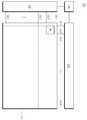
도 4는 도 3의 일부분에 대한 어레이 기판 평면도이다. 도 4는 도 3의 참조번호 310 영역에 대한 도면으로, 다른 부분은 동일한 구조가 반복되는 것으로 이해될 수 있다.4 is an array substrate top view for a portion of FIG. FIG. 4 is a view of the
도 4를 참조하면, 기판 상에 일 방향으로 제1 게이트 라인(410a)이 위치하고, 제1 게이트 라인(410a)과 교차하는 방향으로 제1 데이터 라인(420a)이 위치한다. 제1 데이터 라인(420a)의 우측에는 제1 화소전극(444a) 및 제1 트랜지스터(430a)가 위치하여 제1 화소를 구성한다.Referring to FIG. 4, a
또한, 기판 상에는 제1 게이트 라인(410a)과 나란하게 제2 게이트 라인(410b)이 위치하고, 제1 데이터 라인(420a)과 나란하게 제2 데이터 라인(420b)이 위치한다. 제2 데이터 라인(420b)의 좌측에는 제2 화소전극(444b) 및 제2 트랜지스터(430b)가 위치하여 제2 화소를 구성한다.The
도 4를 참조하면, 제1 트랜지스터(430a)와 제2 트랜지스터(430b)는 좌우가 대칭인 형상으로 서로 다른 방향으로 형성된다.Referring to FIG. 4, the
제1 트랜지스터(430a)는 좌측에 있는 제1 데이터 라인(420a)의 일부분으로 'I'자 형상을 가지는 제1 소스 전극(422a), 일측이 이러한 제1 소스 전극(422a)과 나란하면서 타측은 볼록한 'T'자 모양을 가지는 제1 드레인 전극(432a) 및 제1 게이트 전극(412a)을 포함하여 제1 화소의 좌하측에 형성된다.The
제2 트랜지스터(430b)는 우측에 있는 제2 데이터 라인(420b)의 일부분으로 'I'자 형상을 가지는 제2 소스 전극(422b), 일측이 이러한 제2 소스 전극(422b)과 나란하면서 타측은 볼록한 'T'자 모양을 가지는 제2 드레인 전극(432b) 및 제2 게이트 전극(412b)을 포함하여 제2 화소의 우하측에 형성된다.The
이렇게 Z-인버전 방식의 표시장치(100)에서는 상하로 인접한 화소들의 트랜지스터의 방향이 상이하게 형성된다. 앞서 설명한 바와 같이 화소별로 트랜지스터의 방향이 상이하면 게이트 전극층과 소스/드레인 전극층의 어긋남으로 Cgs의 편차가 발생할 가능성이 있다.In the Z-
도 4의 어레이 기판에서는 이러한 Cgs 편차 발생의 문제를 해소하기 위해 드레인 전극이 게이트 라인에 완전히 오버랩되는 구조를 가진다.The array substrate of FIG. 4 has a structure in which the drain electrode completely overlaps the gate line in order to solve the problem of Cgs deviation.
도 4를 참조하면, 제1 트랜지스터(430a)의 제1 드레인 전극(432a)은 제1 게이트 라인(410a)과 완전히 오버랩된다. 이러한 오버랩되는 형상을, 도 4의 평면도 상에서 보면, 제1 트랜지스터(430a)의 제1 드레인 전극(432a) 영역이 제1 게이트 라인(410a) 영역에 완전히 포함되는 것으로 나타난다.Referring to FIG. 4, the
또한, 제1 드레인 전극(432a)은 제1 게이트 라인(410a)과 마진을 두고 오버랩될 수 있다. 마진을 두고 오버랩된다는 것은, 도 4의 평면도 상에서 볼 때, 제1 드레인 전극(432a)이 제1 게이트 라인(410a)의 가장자리로부터 마진 거리(C) 안쪽에 위치한다는 것을 의미한다.In addition, the
참조번호 433a는 공정상의 문제로 제1 드레인 전극이 일정 거리만큼 어긋나서 다른 위치에 형성된 것을 나타낸다. 이를 제1 드레인 전극'(433a)라고 할 때, 어긋난 거리가 마진 거리(C)보다 작기 때문에 제1 드레인 전극'(433a)은 여전히 제1 게이트 라인(410a)과 완전히 오버랩되고 있다.
도 4의 평면도 상에서, 제1 드레인 전극(432a)과 제1 드레인 전극'(433a)를 비교할 때, 두 전극(432a 및 433a)이 제1 게이트 라인(410a)과 오버랩되는 면적이 동일하다. 이에 따라, 각각의 전극(432a 및 433a)이 제1 게이트 라인(410a)과 형성하는 Cgs의 크기도 동일하게 되어 Cgs 편차 발생의 문제가 해소되게 된다.4, when the
제1 트랜지스터(430a)와 대칭적인 구조를 가지는 제2 트랜지스터(430b)에서도 마찬가지로 제2 드레인 전극(432b)이 제2 게이트 라인(410b)과 완전히 오버랩된다. 이러한 오버랩되는 형상을, 도 4의 평면도 상에서 보면, 제2 트랜지스터(430b)의 제2 드레인 전극(432b) 영역이 제2 게이트 라인(410b) 영역에 완전히 포함되는 것으로 나타난다. 그리고, 제2 드레인 전극(432b)은 제1 드레인 전극(432a)과 마찬가지 방식으로 제2 게이트 라인(410b)과 마진을 두고 오버랩될 수 있다.The
한편, 도 4에 도시된 어레이 기판에서 소스 전극도 게이트 라인에 완전히 오버랩될 수 있다.On the other hand, in the array substrate shown in Fig. 4, the source electrode can also completely overlap the gate line.
도 4를 참조하면, 제1 트랜지스터(430a)의 제1 소스 전극(422a)은 제1 데이터 라인(420a)의 일부분으로 'I'자 형상을 가지고 있다. 이렇게 데이터 라인의 일부분으로 소스 전극이 형성되는 경우, 소스 전극의 영역은 데이터 라인 방향으로 데이터 라인과 게이트 라인이 오버랩되는 부분으로 정의될 수 있다. 제1 소스 전극(422a)의 경우, 제1 데이터 라인(420a)이 제1 게이트 라인(410a)과 오버랩되는 제1 소스 전극 영역(423a)에 해당되는 부분이 제1 소스 전극(422a)에 해당된다.Referring to FIG. 4, the
도 4를 참조하면, 제1 소스 전극(422a)은 제1 데이터 라인(420a)의 일부분으로 'I'자 형상을 가지기 때문에 데이터 라인 방향으로 항상 제1 게이트 라인(410a)과 오버랩된다. 이에 반해, 게이트 라인 방향에서는 제1 소스 전극(422a)의 위치에 따라 제1 소스 전극(422a)이 제1 게이트 라인(410a)과 오버랩되거나 오버랩되지 않을 수 있는데, 도 4에 도시된 어레이 기판에서 제1 소스 전극(422a)은 제1 게이트 라인(410a)과 완전히 오버랩되도록 위치한다. 전술한 바와 같이 이러한 오버랩 관계는 평면도 상에서 확인할 수 있는데, 도 4를 참조하면, 제1 소스 전극(422a) 영역이 제1 게이트 라인(410a) 영역에 포함되는 것으로 나타난다.Referring to FIG. 4, the
자세한 설명은 생략하나 제1 소스 전극(422a)과 같은 방식으로 제2 소스 전극(422b)도 제2 게이트 라인(410b)과 완전히 오버랩된다.A detailed description is omitted, but the
이렇게 소스 전극이 게이트 라인과 완전히 오버랩되면 소스 전극과 게이트 라인 사이에 형성되는 캐패시턴스(Cgd)의 크기가 화소별로 일정하게 유지된다. 소스 전극과 게이트 라인 사이의 캐패시턴스(Cgd)도 Cgs와 마찬가지로 화소에 충전되는 충전 전압을 낮추기 때문에 모든 화소에서 Cgd의 크기가 균일할 필요가 있다. 도 4에 도시된 어레이 기판에서는 이러한 Cgd가 화소별로 균일하게 유지될 수 있어 화소간 불균형으로 인해 발생하는 플리커링이나 세로선의 문제가 해소되게 된다.When the source electrode is completely overlapped with the gate line, the magnitude of the capacitance Cgd formed between the source electrode and the gate line is maintained constant for each pixel. The capacitance Cgd between the source electrode and the gate line also needs to be uniform in the size of Cgd in all the pixels because the charge voltage charged in the pixel is lowered as in the case of Cgs. In the array substrate shown in FIG. 4, such Cgd can be uniformly maintained for each pixel, thereby eliminating the problem of flickering or vertical lines caused by the imbalance between pixels.
소스 전극과 드레인 전극이 게이트 라인과 완전히 오버랩되면, 소스 전극과 드레인 전극 사이에 위치하는 채널도 게이트 라인과 완전히 오버랩된다.If the source electrode and the drain electrode completely overlap the gate line, the channel located between the source electrode and the drain electrode also completely overlaps the gate line.
도 4를 참조하면, 제1 소스 전극(422a)과 제1 드레인 전극(432a) 사이에 위치하는 제1 채널(451a)은 제1 게이트 라인(410a)과 완전히 오버랩되도록 위치한다. 이러한 제1 채널(451a)은 제1 소스 전극(422a)과 제1 드레인 전극(432a)이 제1 게이트 라인(410a)과 완전히 오버랩되기 때문에 자동적으로 제1 게이트 라인(410a)과 오버랩될 수도 있지만, 설계에 의한 위치 조정에 따라 제1 채널(451a) 자체적으로 제1 게이트 라인(410a)과 완전히 오버랩되도록 위치할 수 있다.Referring to FIG. 4, a
채널은 게이트 라인과 오버랩되는 면적에 따라 특성이 달라질 수 있는데, 도 4에 도시된 것과 모든 화소에서 채널이 게이트 라인과 완전히 오버랩되면, 모든 화소의 채널 특성이 동일해 지는 효과가 있다.The characteristics of the channel can be changed according to the area overlapping with the gate line. If the channel completely overlaps with the gate line in all the pixels shown in FIG. 4, the channel characteristics of all the pixels are equalized.
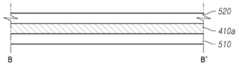
도 5는 도 4의 B-B'를 절단한 단면도이다.5 is a cross-sectional view taken along the line B-B 'in FIG.
도 5를 참조하면, 유기 기판과 같은 기판(510) 상에 금속층 혹은 금속패턴으로 제1 게이트 라인(410a)이 형성되고, 제1 게이트 라인(410a) 상에는 게이트 절연층(520, Gate Insulator; GI)이 형성된다. 게이트 절연층(520) 상부에는 박막트랜지스터의 채널을 이루는 반도체층(530)이 형성되고, 그 상부에는 제1 소스 전극(422a) 및 제1 드레인 전극(432a)을 형성하는 금속층 혹은 금속패턴이 적층된다.5, a
제1 소스 전극(422a) 및 제1 드레인 전극(432a) 상에는 제1보호층(532)이 형성된다. 제1보호층(532)은 질화실리콘(SiNx) 또는 산화실리콘(SiO2) 등과 같은 무기 절연재료로 형성되는 무기 보호층일 수 있으나, 포토-아크릴(Photo-Acryl), 아크릴레이트(Acrylate), 폴리아미드(Pilyamide) 등과 같은 재료로 형성되는 유기 보호층일 수도 있다. 경우에 따라서는 제1보호층(532)이 무기 보호층과 유기 보호층을 이중으로 포함하는 구조를 가질 수도 있다.A
제1보호층(532)에는 제1 콘택홀(442a)이 형성된다. 그리고, 이러한 제1 콘택홀(442a)을 통해 제1 화소전극(444a)이 제1 드레인 전극(432a)과 전기적으로 연결되게 된다.A
제1 화소전극(444a) 상에는 제2보호층(540)이 형성되는데, 이러한 제2보호층(540)은 질화실리콘(SiNx) 또는 산화실리콘(SiO2) 등과 같은 무기 절연재료로 형성되는 무기 보호층일 수 있다.A
도 5에는 설계치에 따른 위치에 형성되는 제1 드레인 전극(432a)과 설계치에서 다소 이동하여 형성되는 제1 드레인 전극'(433a)이 함께 도시되어 있다. 그리고, 이러한 제1 드레인 전극(432a)과 제1 게이트 라인(410a)이 형성하는 Cgs(550)와 제1 드레인 전극'(433a)과 제1 게이트 라인(410a)이 형성하는 Cgs'(551)가 비교를 위해 함께 도시되어 있다.In FIG. 5, the
도 5를 참조하면, 설계치에 위치하는 제1 드레인 전극(432a)과 다소 이동되어 위치하는 제1 드레인 전극'(433a)이 제1 게이트 라인(410a)과 오버랩되는 면적이 동일하다. 이는 제1 드레인 전극(432a)이 제1 게이트 라인(410a)에 완전히 오버랩되기 때문이다. 좀더 구체적으로 설명하면, 도 5의 단면도 상에서 보면, 제1 드레인 전극(432a) 영역 및 제1 드레인 전극'(433a) 영역이 모두 제1 게이트 라인(410a)의 영역에 포함되기 때문이다. 이에 따라, 설계치에 위치하는 제1 드레인 전극(432a)에 의해 형성되는 Cgs(550)의 크기와 제1 드레인 전극'(433a)에 의해 형성되는 Cgs'(551)의 크기도 동일해지게 된다.Referring to FIG. 5, the
도 5를 참조하면, 제1 소스 전극(422a)와 반도체층(530)도 제1 게이트 라인(410a)과 완전히 오버랩되는 것을 확인할 수 있다.Referring to FIG. 5, it can be seen that the
도 6a 내지 도 6d는 도 4의 어레이 기판에 대한 제조공정을 B-B' 절단면으로 나타낸 도면이다.6A to 6D are cross-sectional views of the array substrate of FIG. 4 taken along line BB '.
도 6a를 참조하면, 유기 기판과 같은 기판(510) 상에 금속층 혹은 금속패턴으로 제1 게이트 라인(410a)이 형성되고, 제1 게이트 라인(410a) 상에는 게이트 절연층(520, Gate Insulator; GI)이 형성된다. 이때, 게이트 절연층(520)은 무기절연물질, 예를 들면 산화실리콘, 질화실리콘 또는 이들의 다중층으로부터 선택된 하나일 수 있다. 그리고, 제1 게이트 라인(410a)을 형성하는 금속층은 구리(Cu), 구리 합금, 알루미늄(Al), 알루미늄 합금(AlNd), 몰리브덴(Mo) 및 몰리브덴 합금(MoTi) 중 선택된 하나 또는 둘 이상의 물질을 증착함으로써 단일층 또는 다층 구조를 가질 수 있다.6A, a
도 6b를 참조하면, 게이트 절연층(520) 상에는 반도체층(530)이 형성된다. 반도체층(530)은 P형 불순물 또는 N형 불순물을 도핑하여 소오스 영역 및 드레인 영역을 형성하고, 이와 동시에 소오스 영역 및 드레인 영역 사이에 개재된 채널영역을 정의할 수 있다. P타입 트랜지스터의 경우는 도핑되는 불순물로 붕소(B), 알루미늄(Al), 갈륨(Ga) 및 인듐(In) 등의 3족의 원소가 사용될 수 있으며, N타입 트랜지스터의 경우는 도핑되는 불순물로 인(P), 비소(As) 및 안티몬(Sb) 등의 5족의 원소가 사용될 수 있다. P타입의 트랜지스터는 캐리어로서 정공이 이용되며, N타입의 트랜지스터는 캐리어로서 전자가 이용된다.Referring to FIG. 6B, a
도 6c를 참조하면, 반도체층(530) 상에 소스/드레인 금속막이 형성되고, 마스크 공정을 이용하여 제1 소스 전극(422a) 및 제1 드레인 전극(432a)을 패터닝한다. 이때, 제1 소스 전극(422a) 혹은 제1 드레인 전극(432a)은 구리(Cu), 구리 합금, 알루미늄(Al), 알루미늄 합금(AlNd) 등과 같은 저저항 특성을 갖는 금속물질로 형성될 수 있다.Referring to FIG. 6C, a source / drain metal layer is formed on the
그런데, 이러한 공정에서 도 6c에 도시된 것과 같이 전극 패터닝을 위한 마스크가 다소 이동할 수 있다. 이렇게 마스크가 다소 이동되면, 설계치의 위치에 해당되는 제1 드레인 전극(432a)이 형성되지 않고 설계치에서 다소 이동한 제1 드레인 전극'(433a)이 형성될 수 있다. 이에 따라, Cgs(550)도 Cgs'(551)의 형태로 형성될 수 있다.However, in this process, the mask for electrode patterning can be moved somewhat as shown in FIG. 6C. When the mask is slightly moved, the
제1 실시예에서는 Cgs(550)와 Cgs'(551)의 크기를 동일하게 유지하기 위해 제1 드레인 전극(432a)이 제1 게이트 라인(410a)과 완전히 오버랩되어 위치하도록 제1 드레인 전극(432a)을 형성한다. 실시예에 따라서는, 평면도 상에서 제1 드레인 전극(432a) 영역이 제1 게이트 라인(410a) 영역의 가장자리로부터 마진 거리 안쪽으로 형성되도록 제1 드레인 전극(432a)을 형성한다. 여기서, 마진 거리는 마스크 공정의 오차 범위에 따라 결정된다.The
도 6d를 참조하면, 제1 소스 전극(422a) 및 제1 드레인 전극(432a) 상에는 제1보호층(532)이 형성된다. 그리고, 제1보호층(532)에는 제1 콘택홀(442a)이 형성되고, 제1 콘택홀(442a)을 통해 제1 드레인 전극(432a)과 연결되는 제1 화소전극(444a)이 제1보호층(532) 상에 형성되면, 제1 화소전극(444a) 상에는 제2보호층(540)이 형성된다. 제1보호층(532) 혹은 제2보호층(540)은 질화실리콘(SiNx) 또는 산화실리콘(SiO2) 등과 같은 무기 절연재료로 형성되는 무기 보호층일 수 있으나, 포토-아크릴(Photo-Acryl), 아크릴레이트(Acrylate), 폴리아미드(Pilyamide) 등과 같은 재료로 형성되는 유기 보호층일 수도 있다. 경우에 따라서는 제1보호층(532) 혹은 제2보호층(540)이 무기 보호층과 유기 보호층을 이중으로 포함하는 구조를 가질 수도 있다.Referring to FIG. 6D, a
도 7은 일 실시예에 따른 표시장치의 개구영역을 나타내는 도면이다.7 is a view showing an opening region of a display device according to an embodiment.
도 7의 (a)는 비교 대상이 되는 어레이 기판의 평면도이고, 도 7의 (b)는 일 실시예에 따른 어레이 기판의 평면도이다.7 (a) is a plan view of an array substrate to be compared, and Fig. 7 (b) is a plan view of an array substrate according to an embodiment.
도 7의 (a)를 참조하면, 비교 대상 어레이 기판에서 소스 전극(722a)은 'L'자 모양으로 일부가 게이트 라인 방향으로 돌출되어 있다. 이러한 형상으로 인해, 비교 대상 어레이 기판에서 화소전극(740a)을 연결시키는 콘택홀(734a)은 게이트 전극(712a)의 데이터 라인 방향 가장자리보다 더 위쪽에 형성된다. 이렇게 콘택홀(734a)의 위치가 위로 올라가게 되면 그 만큼 개구영역이 좁아지는 문제가 있다.Referring to FIG. 7A, the
도 7의 (b)를 참조하면, 일 실시예에 따른 어레이 기판에서 소스 전극(722b)은 'I'자 모양으로 형성된다. 이렇게 소스 전극(722b)이 'I'자 모양으로 형성되기 때문에 소스 전극(722b)이 게이트 라인 방향으로 차지하는 공간이 작아져 상대적으로 트랜지스터의 다른 구성이 형성될 공간이 넓어진다. 이에 따라, 드레인 전극(732b)은 위쪽 방향으로 올라가지 않고 게이트 라인과 나란한 방향으로 형성된다. 이에 따라, 일 실시예에 따른 어레이 기판에서 콘택홀(734b)은 게이트 전극(712b)의 데이터 라인 방향 가장자리보다 더 아래쪽에 형성되게 된다. 이렇게 콘택홀(734b)의 위치가 아래 쪽으로 내려오게 되면 그 만큼 개구영역이 넓어지게 된다. 특히, 고해상도 패널에서 각 화소의 면적이 작아지는데, 이러한 패널에서 소스 전극을 일 실시예와 같이 'I'자 모양으로 형성하면 개구율을 좀더 높일 수 있게 된다.Referring to FIG. 7B, in the array substrate according to the embodiment, the
도 8은 도 2의 패널에 적용될 수 있는 다른 어레이 기판의 화소 구조도이다.8 is a pixel structure diagram of another array substrate which can be applied to the panel of Fig.
도 8을 참조하면, 박막트랜지스터들이 Z-인버전 방식과 같이 데이터 라인의 좌측과 우측으로 교번하면서 연결된다. 도 8에 도시된 어레이 기판이 도 3에 도시된 어레이 기판과 다른 점은 박막트랜지스터들이 게이트 라인에 대해서도 상측과 하측으로 교번하면서 연결된다는 것이다.Referring to FIG. 8, the thin film transistors are alternately connected to the left and right sides of the data line like the Z-in version. The difference between the array substrate shown in FIG. 8 and the array substrate shown in FIG. 3 is that the thin film transistors are alternately connected to the gate lines on the upper and lower sides.
이렇게 박막트랜지스터가 게이트 라인의 상측과 하측으로 서로 다른 방향으로 위치하면 종래의 Z-인버전 화소 구조와 마찬가지로 마스크의 어긋남으로 인해 상하 방향으로 Cgs 혹은 Cgd의 편차가 발생할 수 있다.If the thin film transistors are positioned in different directions on the upper and lower sides of the gate line, a deviation of Cgs or Cgd may occur in the vertical direction due to mask misalignment as in the conventional Z-inversion pixel structure.
그런데, 이러한 문제는 본 발명의 일 실시예 개념을 적용함으로써 해소될 수 있다. 일 실시예의 개념은 드레인 전극 혹은 소스 전극을 게이트 라인과 완전히 오버랩되도록 위치시키는 것이다. 이렇게 드레인 전극 혹은 소스 전극이 게이트 라인과 완전히 오버랩되면 마스크의 어긋남의 상하 방향(데이터 라인 방향)으로 나타나더라도 Cgs 혹은 Cgd에는 편차가 발생하지 않게 된다.However, such a problem can be overcome by applying the concept of an embodiment of the present invention. The concept of one embodiment is to position the drain electrode or the source electrode so as to completely overlap the gate line. If the drain electrode or the source electrode completely overlaps with the gate line, no deviation occurs in Cgs or Cgd even when the mask appears in the vertical direction (data line direction) of shift of the mask.
이상과 같이, 소스 전극 및/또는 드레인 전극이 게이트 라인과 완전히 오버랩되도록 위치하면 각 화소에서의 Cgs를 실질적으로 동일하게 유지하는 효과가 있다.As described above, when the source electrode and / or the drain electrode are positioned so as to completely overlap the gate line, there is an effect that Cgs in each pixel is maintained substantially equal.
이렇게 화소별로 Cgs의 크기가 실질적으로 동일하게 유지되면, 하나의 표시장치 관점에서, 화소간 불균형이 제거되고 플리커링이나 세로선 불량의 문제가 개선되는 효과가 있다. 특히, Z 인버전 방식이나 게이트 라인의 상측과 하측으로 트랜지스터가 교번하는 화소 구조에서는 공정상의 오차에 따라 화소별로 Cgs가 달라질 가능성이 있는데, 본 발명의 실시예에 따르면 이러한 화소 구조에서도 Cgs가 균일하게 유지되는 효과가 있다.Thus, when the size of Cgs is kept substantially the same for each pixel, the imbalance between pixels is removed from the viewpoint of one display device, and the problem of flickering and vertical line defect is improved. In particular, according to the Z-inversion method or the pixel structure in which the transistors are alternately arranged on the upper and lower sides of the gate line, there is a possibility that the Cgs varies depending on the process error. According to the embodiment of the present invention, There is an effect to be maintained.
양산 라인의 관점에서 살펴보면, 제품별 Cgs의 크기가 동일하게 유지됨으로써, 제품 사이의 특성이 균일하게 유지되고 품질 관리가 용이해지는 효과가 있다. 특히, 종래 양산 라인에서, Cgs의 변동을 조절하기 위해 Cgs 보상 패턴을 적용하거나 각 제품에 대한 Cgs 미세 조정 작업을 수행하였는데, 본 발명에 의하면, 이러한 부차적인 공정이 제거되는 효과가 있다.From the viewpoint of the mass production line, the size of Cgs for each product is maintained to be the same, so that characteristics between the products are uniformly maintained and quality control is facilitated. Particularly, in the conventional mass production line, the Cgs compensation pattern is applied to adjust the variation of the Cgs, or the Cgs fine adjustment operation is performed for each product. According to the present invention, this additional process is eliminated.
도 9는 일반적인 Cgs 보상 과정의 흐름을 나타내는 도면이다.9 is a view showing a flow of a general Cgs compensation process.
도 9의 (a)는 종래의 컬럼 인버전 화소 구조를 가지는 표시장치에서의 Cgs 보상 과정이고, 도 9의 (b)는 종래의 Z-인버전 화소 구조를 가지는 표시장치에서의 Cgs 보상 과정이다.9A is a Cgs compensation process in a display device having a version pixel structure which is a conventional column, and FIG. 9B is a Cgs compensation process in a display device having a conventional Z-inversion pixel structure .
도 9의 (a)를 참조하면, 종래의 컬럼 인버전 화소 구조를 가지는 표시장치에서는, 컬럼 인버전 화소 구조의 어레이 기판이 형성되고(S1010), Cgs의 크기가 정상 범위 이외에 해당되는 경우, 공통전압(Vcom) 보정을 통해 Cgs가 보상되었다. 컬럼 인버전 화소 구조의 경우, 마스크의 오차가 발생하면 화소 전체의 Cgs가 일관되게 변하게 된다. 따라서, 이 경우에는 하나의 표시장치 내에서 화소간 Cgs 편차는 발생하지 않는다. 다만, Cgs가 정상 범위에서 벗어나면 화소 충전 전압이 전 화소에서 내려가거나 올라가기 때문에 공통전압(Vcom)의 크기를 조절하여 Cgs를 보상해 줘야 하는데, 이에 따라, 종래의 컬럼 인버전 화소 구조를 가지는 표시장치 공정에서는 이러한 공통전압(Vcom) 보정 단계(S1012)가 포함되어 있다.Referring to FIG. 9A, in a display device having a version pixel structure of a conventional column, an array substrate of a version pixel structure is formed (S1010). When the size of the Cgs is outside the normal range, Cgs was compensated through voltage (Vcom) correction. In the case of the column-version pixel structure, if a mask error occurs, the Cgs of the entire pixel is consistently changed. Therefore, in this case, there is no Cgs deviation between pixels in one display device. However, when the Cgs is out of the normal range, the pixel charge voltage is lowered or raised from all the pixels. Therefore, the Cgs must be compensated by adjusting the magnitude of the common voltage Vcom. Accordingly, In the display device process, this common voltage (Vcom) correction step (S1012) is included.
도 9의 (b)를 참조하면, 종래의 Z-인버전 화소 구조를 가지는 표시장치에서는, Z-인버전 화소 구조의 어레이 기판이 형성되고(S1020), Cgs의 크기가 정상 범위 이외에 해당되는 경우, 먼저 보상 패턴을 형성한다(S1022).Referring to FIG. 9B, in a display device having a conventional Z-inversion pixel structure, an array substrate of a Z-in version pixel structure is formed (S1020), and when the size of Cgs is outside the normal range , A compensation pattern is formed first (S1022).
앞서 설명한 바와 같이 종래의 Z-인버전 화소 구조에서 마스크의 어긋남이 발생하면 화소별로 Cgs의 편차가 발생하게 된다. 이를 해결하기 위해서는 Cgs의 크기가 상대적으로 작은 화소에 보상 패턴을 추가하여 Cgs의 크기를 증가시켜야 한다. 이러한 보상 패턴 형성 단계(S1022)를 통해 전체 화소의 Cgs 크기를 균일하게 만든다.As described above, when a mask shift occurs in the conventional Z-inversion pixel structure, a deviation of Cgs occurs for each pixel. To solve this problem, it is necessary to increase the size of Cgs by adding a compensation pattern to a pixel having a relatively small Cgs. In this compensation pattern formation step (S1022), the Cgs size of all the pixels is made uniform.
보상 패턴 형성 단계(S1022)를 통해 전체 화소의 Cgs 크기를 균일하게 만든 후에는 Cgs의 크기가 전체적으로 정상 범위 이외에 있기 때문에 공통전압(Vcom)의 크기를 조절하여 Cgs를 보상해 주게 된다(S1024).After the Cgs size of all the pixels is made uniform through the compensation pattern formation step S1022, the size of the common voltage Vcom is adjusted to compensate the Cgs since the size of the Cgs is outside the normal range as a whole (S1024).
도 9를 참조하면, 종래 방식에서는 공정상에 Cgs를 보상하는 공정이 필요하게 된다. 특히, Z-인버전 방식으로 화소를 형성하는 표시장치의 경우, 보상 패턴 형성 단계(S1022) 및 Vcom 보정 단계(S1024)라는 2가지 단계가 필요하게 된다. 이에 반해, 일 실시예에 따른 표시장치는 Cgs의 보상이 필요없어 이러한 2가지 단계를 스킵할 수 있게 된다.Referring to FIG. 9, in the conventional method, a process of compensating for Cgs is required in the process. Particularly, in the case of a display device that forms pixels in the Z-inversion mode, two steps are required: a compensation pattern formation step (S1022) and a Vcom correction step (S1024). On the other hand, the display device according to the embodiment can skip these two steps since the compensation of Cgs is not necessary.
또한, 최근 표시장치의 해상도가 올라가면서 화소 내의 공간이 좁아지고 있다. 이에 따라, Cgs의 크기를 보상하기 위한 보상 패턴 형성 공간이 줄어드는 추세이다. 이에 따라, 실질적으로 종래의 방식과 같은 Cgs 보상 과정의 수행이 어려워지고 있다. 이러한 측면에서 일 실시예에 따른 표시장치는 Cgs를 보상할 필요가 없어 위와 같은 문제를 해소할 수 있게 된다.In addition, as the resolution of the display device has recently increased, the space in the pixel is narrowed. Accordingly, the compensation pattern forming space for compensating the size of Cgs is reduced. Accordingly, it is practically difficult to perform the Cgs compensation process as in the conventional method. In this respect, the display device according to the embodiment does not need to compensate the Cgs, so that the above problem can be solved.
이상에서 기재된 "포함하다", "구성하다" 또는 "가지다" 등의 용어는, 특별히 반대되는 기재가 없는 한, 해당 구성 요소가 내재될 수 있음을 의미하는 것이므로, 다른 구성 요소를 제외하는 것이 아니라 다른 구성 요소를 더 포함할 수 있는 것으로 해석되어야 한다. 기술적이거나 과학적인 용어를 포함한 모든 용어들은, 다르게 정의되지 않는 한, 본 발명이 속하는 기술 분야에서 통상의 지식을 가진 자에 의해 일반적으로 이해되는 것과 동일한 의미를 가진다. 사전에 정의된 용어와 같이 일반적으로 사용되는 용어들은 관련 기술의 문맥 상의 의미와 일치하는 것으로 해석되어야 하며, 본 발명에서 명백하게 정의하지 않는 한, 이상적이거나 과도하게 형식적인 의미로 해석되지 않는다.It is to be understood that the terms "comprises", "comprising", or "having" as used in the foregoing description mean that the constituent element can be implanted unless specifically stated to the contrary, But should be construed as further including other elements. All terms, including technical and scientific terms, have the same meaning as commonly understood by one of ordinary skill in the art to which this invention belongs, unless otherwise defined. Commonly used terms, such as predefined terms, should be interpreted to be consistent with the contextual meanings of the related art, and are not to be construed as ideal or overly formal, unless expressly defined to the contrary.
이상의 설명은 본 발명의 기술 사상을 예시적으로 설명한 것에 불과한 것으로서, 본 발명이 속하는 기술 분야에서 통상의 지식을 가진 자라면 본 발명의 본질적인 특성에서 벗어나지 않는 범위에서 다양한 수정 및 변형이 가능할 것이다. 따라서, 본 발명에 개시된 실시예들은 본 발명의 기술 사상을 한정하기 위한 것이 아니라 설명하기 위한 것이고, 이러한 실시예에 의하여 본 발명의 기술 사상의 범위가 한정되는 것은 아니다. 본 발명의 보호 범위는 아래의 청구범위에 의하여 해석되어야 하며, 그와 동등한 범위 내에 있는 모든 기술 사상은 본 발명의 권리범위에 포함되는 것으로 해석되어야 할 것이다.
The foregoing description is merely illustrative of the technical idea of the present invention and various changes and modifications may be made by those skilled in the art without departing from the essential characteristics of the present invention. Therefore, the embodiments disclosed in the present invention are intended to illustrate rather than limit the scope of the present invention, and the scope of the technical idea of the present invention is not limited by these embodiments. The scope of protection of the present invention should be construed according to the following claims, and all technical ideas within the scope of equivalents should be construed as falling within the scope of the present invention.
Claims (16)
Translated fromKorean기판 상에 화소 영역을 정의하기 위해 서로 교차하여 배치되는 게이트 라인과 데이터 라인;
게이트 전극, 반도체층, 소스 전극 및 드레인 전극을 포함하고, 평면도 상에서 드레인 전극 영역이 게이트 라인 영역에 완전히 포함되도록 상기 드레인 전극이 게이트 라인과 완전히 오버랩되는 박막트랜지스터; 및
상기 화소 영역 내에 배치되며 상기 박막트랜지스터의 상기 드레인 전극과 전기적으로 연결되는 화소 전극을 포함하며,
상기 박막트랜지스터의 드레인 전극은 상기 소스 전극과 인접한 일측이 상기 소스 전극과 나란하고 타측은 볼록한 T자 모양을 가지며,
상기 화소 전극은 상기 박막트랜지스터의 드레인 전극의 타측 상에 위치하는 콘택홀을 통해 상기 박막트랜지스터의 드레인 전극과 전기적으로 연결되는,
Z-인버전 방식의 표시장치.A display device in which pixels are formed in a Z-inversion manner,
A gate line and a data line arranged to cross each other to define a pixel region on the substrate;
A thin film transistor including a gate electrode, a semiconductor layer, a source electrode, and a drain electrode, the drain electrode completely overlapping the gate line so that the drain electrode region is completely included in the gate line region; And
And a pixel electrode disposed in the pixel region and electrically connected to the drain electrode of the thin film transistor,
The drain electrode of the thin film transistor has a side adjacent to the source electrode parallel to the source electrode and a convex T shape on the other side,
Wherein the pixel electrode is electrically connected to a drain electrode of the thin film transistor through a contact hole located on the other side of the drain electrode of the thin film transistor,
Z-in version display device.
평면도 상에서 콘택홀 영역이 게이트 라인 영역에 완전히 포함되도록 상기 콘택홀이 게이트 라인과 완전히 오버랩되는 것을 특징으로 하는 Z-인버전 방식의 표시장치.The method according to claim 1,
Wherein the contact hole completely overlaps with the gate line so that the contact hole region is completely included in the gate line region on the plan view.
평면도 상에서, 상기 박막트랜지스터의 드레인 전극은 게이트 라인의 가장자리로부터 마진 거리 안쪽에 위치하는 것을 특징으로 하는 Z-인버전 방식의 표시장치.The method according to claim 1,
Wherein the drain electrode of the thin film transistor is located within a margin distance from the edge of the gate line on a plan view.
상기 박막트랜지스터의 소스 전극과 드레인 전극 사이의 채널은 게이트 라인과 완전히 오버랩되는 것을 특징으로 하는 Z-인버전 방식의 표시장치.The method according to claim 1,
Wherein the channel between the source electrode and the drain electrode of the thin film transistor completely overlaps the gate line.
상기 데이터 라인의 일부분 혹은 일부분이 확장되어 배치되는 상기 박막트랜지스터의 소스 전극은 I자 모양을 가지는 것을 특징으로 하는 Z-인버전 방식의 표시장치.The method according to claim 1,
And the source electrode of the thin film transistor in which a part or a part of the data line is extended is I-shaped.
상기 콘택홀 영역을 포함하는 게이트 라인 영역의 데이터 라인 방향 폭은 상기 드레인 전극의 일측을 포함하는 게이트 라인 영역의 데이터 라인 방향 폭과 상이한 것을 특징으로 하는 Z-인버전 방식의 표시장치.3. The method of claim 2,
And the data line direction width of the gate line region including the contact hole region is different from the data line direction width of the gate line region including one side of the drain electrode.
기판 상에 게이트 라인 및 게이트 전극을 형성하는 단계;
상기 게이트 전극 상으로 게이트 절연층, 반도체층 및 소스/드레인 금속막을 순차적으로 형성하고, 마스크 공정에 따라 소스 전극, 드레인 전극 및 데이터 라인을 형성하며, 평면도 상에서 드레인 전극 영역이 게이트 라인 영역에 완전히 포함되고, 소스 전극과 인접한 일측이 상기 소스 전극과 나란하고 타측은 볼록한 T자 모양을 가지도록 상기 드레인 전극을 형성하는 단계;
상기 드레인 전극 상에 제1 보호층을 형성하고, 상기 드레인 전극의 타측 상에 위치하는 상기 제1 보호층에 콘택홀을 형성하는 단계; 및
상기 콘택홀이 형성된 제1 보호층 상에 화소 전극을 형성하고 상기 화소 전극 상에 제2 보호층을 형성하는 단계
를 포함하는 Z-인버전 방식의 표시장치 제조방법.A method of manufacturing a display device of a Z-in version system,
Forming a gate line and a gate electrode on the substrate;
Forming a source electrode, a drain electrode, and a data line in accordance with a mask process; and forming a drain electrode region on the gate electrode entirely in the gate line region Forming the drain electrode such that one side adjacent to the source electrode is parallel to the source electrode and the other side has a convex T shape;
Forming a first passivation layer on the drain electrode and forming a contact hole in the first passivation layer on the other side of the drain electrode; And
Forming a pixel electrode on the first passivation layer on which the contact hole is formed and forming a second passivation layer on the pixel electrode
Wherein the Z-type display device is a Z-type display device.
상기 마스크 공정의 오차 범위에 따라 결정되는 마진 거리에 대하여 평면도 상에서 드레인 전극이 게이트 라인의 가장자리로부터 상기 마진 거리 안쪽에 위치하도록 상기 드레인 전극을 형성하는 것을 특징으로 하는 Z-인버전 방식의 표시장치 제조방법.8. The method of claim 7,
Wherein the drain electrode is formed so that the drain electrode is located inside the margin distance from the edge of the gate line on a plan view with respect to a margin distance determined according to an error range of the mask process. Way.
상기 소스 전극을 데이터 라인의 일부분을 포함하여 I자 모양으로 형성하는 것을 특징으로 하는 Z-인버전 방식의 표시장치 제조방법.8. The method of claim 7,
Wherein the source electrode is formed in an I-shape including a part of a data line.
게이트 전극, 반도체층, 소스 전극 및 드레인 전극을 포함하고, 평면도 상에서 드레인 전극 영역이 게이트 라인 영역에 완전히 포함되도록 상기 드레인 전극이 게이트 라인과 완전히 오버랩되는 박막트랜지스터; 및
상기 화소 영역 내에 배치되며 상기 박막트랜지스터의 상기 드레인 전극과 전기적으로 연결되는 화소 전극을 포함하며,
상기 박막트랜지스터는 좌우가 대칭인 형상을 가지며, 상기 데이터 라인의 방향을 따라 일측 및 타측으로 교번하면서 상기 데이터 라인과 연결되도록 배치되는 제1 박막트랜지스터 및 제2 박막트랜지스터를 포함하며,
상기 제1 박막트랜지스터의 드레인 전극은 일측이 소스 전극과 나란하도록 반시계 방향으로 90도 회전한 T자 모양을 가지며,
상기 제2 박막트랜지스터의 드레인 전극은 타측이 소스 전극과 나란하도록 시계 방향으로 90도 회전한 T자 모양을 가지며,
평면도 상에서 소스 전극 영역이 게이트 라인 영역에 완전히 포함되도록 상기 소스 전극이 게이트 라인과 완전히 오버랩되는 Z-인버전 방식의 표시장치.A gate line and a data line arranged to cross each other to define a pixel region on the substrate;
A thin film transistor including a gate electrode, a semiconductor layer, a source electrode, and a drain electrode, the drain electrode completely overlapping the gate line so that the drain electrode region is completely included in the gate line region; And
And a pixel electrode disposed in the pixel region and electrically connected to the drain electrode of the thin film transistor,
Wherein the thin film transistor includes a first thin film transistor and a second thin film transistor which are symmetrical in the left and right direction and are arranged so as to be connected to the data line alternately to one side and the other side along the direction of the data line,
The drain electrode of the first thin film transistor has a T-shape rotated by 90 degrees counterclockwise so that one side thereof is parallel to the source electrode,
The drain electrode of the second thin film transistor has a T-shaped shape rotated clockwise by 90 degrees so that the other side thereof is parallel to the source electrode,
Wherein the source electrode completely overlaps with the gate line so that the source electrode region completely overlaps the gate line region on the plan view.
상기 화소 전극은 상기 제1 박막트랜지스터의 드레인 전극의 타측 및 상기 제2 박막트랜지스터의 드레인 전극의 일측 상에 위치하는 콘택홀을 통해 상기 박막트랜지스터의 드레인 전극과 전기적으로 연결되는 Z-인버전 방식의 표시장치.11. The method of claim 10,
The pixel electrode is electrically connected to the drain electrode of the thin film transistor through a contact hole located on the other side of the drain electrode of the first thin film transistor and on one side of the drain electrode of the second thin film transistor. Display device.
상기 소스 전극은 상기 데이터 라인의 일부분 혹은 일부분이 확장되어 배치되며, I자 모양을 가지는 Z-인버전 방식의 표시장치.11. The method of claim 10,
Wherein the source electrode is arranged in a part or a part of the data line so as to extend in an I-shape.
상기 소스 전극 영역을 포함하는 게이트 라인 영역의 데이터 라인 방향의 폭은 상기 콘택홀 영역을 포함하는 게이트 라인 영역의 데이터 라인 방향의 폭과 상이한 Z-인버전 방식의 표시장치.12. The method of claim 11,
Wherein the width of the gate line region including the source electrode region in the data line direction is different from the width of the gate line region including the contact hole region in the data line direction.
상기 제1 박막트랜지스터의 드레인 전극이 게이트 전극에 오버랩되는 면적은 상기 제2 박막트랜지스터의 드레인 전극이 게이트 전극에 오버랩되는 면적과 동일한 Z-인버전 방식의 표시장치.11. The method of claim 10,
Wherein the area where the drain electrode of the first thin film transistor overlaps with the gate electrode is the same as the area where the drain electrode of the second thin film transistor overlaps the gate electrode.
상기 제1 박막트랜지스터의 소스 전극과 드레인 전극 사이의 제1 채널 및 상기 제2 박막트랜지스터의 소스 전극과 드레인 전극 사이의 제2 채널은 게이트 라인과 완전히 오버랩되는 Z-인버전 방식의 표시장치.11. The method of claim 10,
Wherein the first channel between the source electrode and the drain electrode of the first thin film transistor and the second channel between the source electrode and the drain electrode of the second thin film transistor completely overlap the gate line.
게이트 전극, 반도체층, 소스 전극 및 드레인 전극을 포함하고, 평면도 상에서 드레인 전극 영역이 게이트 라인 영역에 완전히 포함되도록 상기 드레인 전극이 게이트 라인과 완전히 오버랩되는 박막트랜지스터; 및
상기 화소 영역 내에 배치되며 상기 박막트랜지스터의 상기 드레인 전극과 전기적으로 연결되는 화소 전극을 포함하며,
상기 박막트랜지스터는 좌우가 대칭인 형상을 가지는 제1 박막트랜지스터 및 제2 박막트랜지스터를 포함하며,
상기 제1 박막트랜지스터와 상기 제2 박막트랜지스터는 상기 데이터 라인의 방향을 따라 일측 및 타측으로 교번하면서 상기 데이터 라인과 연결되도록 배치되며,
상기 제1 박막트랜지스터의 게이트 라인의 가장자리로부터 드레인 전극 사이의 제1 간격은 상기 제2 박막트랜지스터의 게이트 라인의 가장자리로부터 드레인 전극 사이의 제2 간격과 상이하며,
상기 제1 박막트랜지스터의 드레인 전극과 게이트 라인이 오버랩되는 면적은 상기 제2 박막트랜지스터의 드레인 전극과 게이트 라인이 오버랩되는 면적과 동일한 Z-인버전 방식의 표시장치.A gate line and a data line arranged to cross each other to define a pixel region on the substrate;
A thin film transistor including a gate electrode, a semiconductor layer, a source electrode, and a drain electrode, the drain electrode completely overlapping the gate line so that the drain electrode region is completely included in the gate line region; And
And a pixel electrode disposed in the pixel region and electrically connected to the drain electrode of the thin film transistor,
Wherein the thin film transistor includes a first thin film transistor and a second thin film transistor having a symmetrical shape on the left and right sides,
Wherein the first thin film transistor and the second thin film transistor are arranged so as to be connected to the data line alternately to one side and the other side along the direction of the data line,
The first interval between the edge of the gate line and the drain electrode of the first thin film transistor is different from the second interval between the edge of the gate line of the second thin film transistor and the drain electrode,
Wherein the area where the drain electrode of the first thin film transistor and the gate line overlap is equal to the area where the drain electrode of the second thin film transistor and the gate line overlap with each other.
Priority Applications (5)
| Application Number | Priority Date | Filing Date | Title |
|---|---|---|---|
| KR1020140052330AKR101539326B1 (en) | 2014-04-30 | 2014-04-30 | Z-inversion Type Display Device and Manufacturing Method thereof |
| US14/699,531US9588386B2 (en) | 2014-04-30 | 2015-04-29 | Z-inversion type display device with ‘T’-shaped electrode and method of manufacturing the same |
| CN201510217541.4ACN105022198B (en) | 2014-04-30 | 2015-04-30 | Z inversion-type display device and the method for manufacturing the Z inversion-type display device |
| EP15165848.1AEP2940520B1 (en) | 2014-04-30 | 2015-04-30 | Z-inversion type display device and method of manufacturing the same |
| US15/411,921US9780126B2 (en) | 2014-04-30 | 2017-01-20 | Z-inversion type display device and method of manufacturing the same |
Applications Claiming Priority (1)
| Application Number | Priority Date | Filing Date | Title |
|---|---|---|---|
| KR1020140052330AKR101539326B1 (en) | 2014-04-30 | 2014-04-30 | Z-inversion Type Display Device and Manufacturing Method thereof |
Publications (1)
| Publication Number | Publication Date |
|---|---|
| KR101539326B1true KR101539326B1 (en) | 2015-07-27 |
Family
ID=53283977
Family Applications (1)
| Application Number | Title | Priority Date | Filing Date |
|---|---|---|---|
| KR1020140052330AActiveKR101539326B1 (en) | 2014-04-30 | 2014-04-30 | Z-inversion Type Display Device and Manufacturing Method thereof |
Country Status (4)
| Country | Link |
|---|---|
| US (2) | US9588386B2 (en) |
| EP (1) | EP2940520B1 (en) |
| KR (1) | KR101539326B1 (en) |
| CN (1) | CN105022198B (en) |
Cited By (2)
| Publication number | Priority date | Publication date | Assignee | Title |
|---|---|---|---|---|
| KR20200022968A (en)* | 2018-08-24 | 2020-03-04 | 엘지디스플레이 주식회사 | Z-inversion type display device |
| KR20210153175A (en) | 2020-06-09 | 2021-12-17 | 삼성디스플레이 주식회사 | Display device |
Families Citing this family (8)
| Publication number | Priority date | Publication date | Assignee | Title |
|---|---|---|---|---|
| KR102503164B1 (en)* | 2016-04-05 | 2023-02-24 | 삼성디스플레이 주식회사 | Display panel and method of manufacturing the same |
| CN106169483B (en)* | 2016-07-01 | 2019-03-15 | 京东方科技集团股份有限公司 | Array substrate and preparation method thereof, and display device |
| KR102725326B1 (en)* | 2016-12-21 | 2024-11-01 | 엘지디스플레이 주식회사 | Organic light emitting diode display device |
| JP6998740B2 (en)* | 2017-11-16 | 2022-01-18 | パナソニック液晶ディスプレイ株式会社 | Liquid crystal display panel |
| US11257455B2 (en)* | 2020-03-22 | 2022-02-22 | Shenzhen China Star Optoelectronics Semiconductor Display Technology Co., Ltd. | Gate drive circuit and display panel |
| US12232374B2 (en)* | 2020-08-31 | 2025-02-18 | Chengdu Boe Optoelectronics Technology Co., Ltd. | Display substrate and display device |
| CN114488591B (en) | 2020-10-23 | 2024-07-09 | 北京京东方显示技术有限公司 | Array substrate and display device |
| CN115799275B (en)* | 2022-12-26 | 2025-07-15 | 厦门天马微电子有限公司 | Display panel and display device |
Citations (4)
| Publication number | Priority date | Publication date | Assignee | Title |
|---|---|---|---|---|
| KR20010105923A (en)* | 2000-05-19 | 2001-11-29 | 구본준, 론 위라하디락사 | Liquid Crystal Dispaly and method for fabricating the same |
| KR20030053241A (en)* | 2001-12-22 | 2003-06-28 | 엘지.필립스 엘시디 주식회사 | Liquid Crystal Display Device and method for manufacturing the same |
| KR20040023276A (en)* | 2002-09-11 | 2004-03-18 | 비오이 하이디스 테크놀로지 주식회사 | Thin film transistor liquid crystal display prevented shot mura |
| KR20090013531A (en)* | 2007-08-02 | 2009-02-05 | 엘지디스플레이 주식회사 | LCD Display |
Family Cites Families (13)
| Publication number | Priority date | Publication date | Assignee | Title |
|---|---|---|---|---|
| US5414283A (en) | 1993-11-19 | 1995-05-09 | Ois Optical Imaging Systems, Inc. | TFT with reduced parasitic capacitance |
| KR0149311B1 (en) | 1995-07-28 | 1998-10-15 | 김광호 | Wafer for lcd device without difference of parasitic capacitance between pixels |
| JP2001051294A (en)* | 1999-08-05 | 2001-02-23 | Internatl Business Mach Corp <Ibm> | High definition tft liquid crystal display device |
| WO2004063805A1 (en) | 2002-12-03 | 2004-07-29 | Quanta Display Inc. | Pixel structure and thin film transistor array |
| KR100918180B1 (en)* | 2003-03-04 | 2009-09-22 | 삼성전자주식회사 | Shift register |
| KR101048365B1 (en)* | 2004-09-09 | 2011-07-11 | 삼성전자주식회사 | Transistors and Display Devices Having the Same |
| US7688392B2 (en)* | 2006-04-06 | 2010-03-30 | Chunghwa Picture Tubes, Ltd. | Pixel structure including a gate having an opening and an extension line between the data line and the source |
| KR101525590B1 (en)* | 2008-10-08 | 2015-06-04 | 삼성디스플레이 주식회사 | Display substrate and manufacturing method thereof |
| JP4743348B2 (en)* | 2009-03-17 | 2011-08-10 | 凸版印刷株式会社 | THIN FILM TRANSISTOR ARRAY AND IMAGE DISPLAY DEVICE USING THIN FILM TRANSISTOR ARRAY |
| CN202049313U (en)* | 2011-05-16 | 2011-11-23 | 京东方科技集团股份有限公司 | Array substrate and thin film transistor liquid crystal display |
| KR101798868B1 (en)* | 2011-06-24 | 2017-12-20 | 엘지디스플레이 주식회사 | Liquid crystal display device and method for manufacturing the same |
| KR20130016922A (en) | 2011-08-09 | 2013-02-19 | 엘지디스플레이 주식회사 | Liquid crystal display device |
| CN103137555B (en)* | 2011-11-30 | 2016-03-09 | 上海中航光电子有限公司 | Thin film transistor LCD device and manufacture method thereof |
- 2014
- 2014-04-30KRKR1020140052330Apatent/KR101539326B1/enactiveActive
- 2015
- 2015-04-29USUS14/699,531patent/US9588386B2/enactiveActive
- 2015-04-30EPEP15165848.1Apatent/EP2940520B1/enactiveActive
- 2015-04-30CNCN201510217541.4Apatent/CN105022198B/enactiveActive
- 2017
- 2017-01-20USUS15/411,921patent/US9780126B2/enactiveActive
Patent Citations (4)
| Publication number | Priority date | Publication date | Assignee | Title |
|---|---|---|---|---|
| KR20010105923A (en)* | 2000-05-19 | 2001-11-29 | 구본준, 론 위라하디락사 | Liquid Crystal Dispaly and method for fabricating the same |
| KR20030053241A (en)* | 2001-12-22 | 2003-06-28 | 엘지.필립스 엘시디 주식회사 | Liquid Crystal Display Device and method for manufacturing the same |
| KR20040023276A (en)* | 2002-09-11 | 2004-03-18 | 비오이 하이디스 테크놀로지 주식회사 | Thin film transistor liquid crystal display prevented shot mura |
| KR20090013531A (en)* | 2007-08-02 | 2009-02-05 | 엘지디스플레이 주식회사 | LCD Display |
Cited By (3)
| Publication number | Priority date | Publication date | Assignee | Title |
|---|---|---|---|---|
| KR20200022968A (en)* | 2018-08-24 | 2020-03-04 | 엘지디스플레이 주식회사 | Z-inversion type display device |
| KR102532090B1 (en)* | 2018-08-24 | 2023-05-12 | 엘지디스플레이 주식회사 | Z-inversion type display device |
| KR20210153175A (en) | 2020-06-09 | 2021-12-17 | 삼성디스플레이 주식회사 | Display device |
Also Published As
| Publication number | Publication date |
|---|---|
| US20150316825A1 (en) | 2015-11-05 |
| CN105022198A (en) | 2015-11-04 |
| EP2940520A1 (en) | 2015-11-04 |
| US9588386B2 (en) | 2017-03-07 |
| EP2940520B1 (en) | 2016-09-21 |
| US20170133405A1 (en) | 2017-05-11 |
| CN105022198B (en) | 2018-11-23 |
| US9780126B2 (en) | 2017-10-03 |
Similar Documents
| Publication | Publication Date | Title |
|---|---|---|
| KR101539326B1 (en) | Z-inversion Type Display Device and Manufacturing Method thereof | |
| CN110060650B (en) | Multiplex type liquid crystal display driving circuit | |
| JP4969568B2 (en) | Display device | |
| US9041625B2 (en) | Subpixel arrangement structure for a display device and display device | |
| JP4578915B2 (en) | Active matrix type liquid crystal display device and liquid crystal display panel used therefor | |
| US8325286B2 (en) | Active matrix substrate and display device including the same | |
| JP6621924B2 (en) | Array substrate and liquid crystal display device | |
| US9019184B2 (en) | Liquid crystal display device including specific subpixel arrangement | |
| US20140091996A1 (en) | Liquid crystal display device including tft compensation circuit | |
| US20050275610A1 (en) | Liquid crystal display device and driving method for the same | |
| WO2007088656A1 (en) | Display | |
| KR101992103B1 (en) | Liquid crystal display and driving method of the same | |
| KR20110067227A (en) | LCD and its driving method | |
| JP2020183970A (en) | Active matrix board and display device | |
| KR102293372B1 (en) | Display Device | |
| KR102045810B1 (en) | Display device | |
| CN116068815A (en) | Display substrate, display panel and display device | |
| KR101901339B1 (en) | liquid crystal display device | |
| KR102524416B1 (en) | Display device | |
| KR102530894B1 (en) | Display device | |
| WO2012077647A1 (en) | Liquid crystal panel, display device, and method for driving the liquid crystal panel | |
| KR20190124036A (en) | Display panel and display device |
Legal Events
| Date | Code | Title | Description |
|---|---|---|---|
| PA0109 | Patent application | Patent event code:PA01091R01D Comment text:Patent Application Patent event date:20140430 | |
| PA0201 | Request for examination | ||
| PE0902 | Notice of grounds for rejection | Comment text:Notification of reason for refusal Patent event date:20150223 Patent event code:PE09021S01D | |
| E701 | Decision to grant or registration of patent right | ||
| PE0701 | Decision of registration | Patent event code:PE07011S01D Comment text:Decision to Grant Registration Patent event date:20150629 | |
| GRNT | Written decision to grant | ||
| PR0701 | Registration of establishment | Comment text:Registration of Establishment Patent event date:20150720 Patent event code:PR07011E01D | |
| PR1002 | Payment of registration fee | Payment date:20150720 End annual number:3 Start annual number:1 | |
| PG1601 | Publication of registration | ||
| FPAY | Annual fee payment | Payment date:20190617 Year of fee payment:5 | |
| PR1001 | Payment of annual fee | Payment date:20190617 Start annual number:5 End annual number:5 | |
| PR1001 | Payment of annual fee | Payment date:20200617 Start annual number:6 End annual number:6 | |
| PR1001 | Payment of annual fee | Payment date:20210614 Start annual number:7 End annual number:7 | |
| PR1001 | Payment of annual fee | Payment date:20240617 Start annual number:10 End annual number:10 | |
| PR1001 | Payment of annual fee | Payment date:20250616 Start annual number:11 End annual number:11 |