KR101539258B1 - Touch display and electronic apparatus - Google Patents
Touch display and electronic apparatusDownload PDFInfo
- Publication number
- KR101539258B1 KR101539258B1KR1020127030635AKR20127030635AKR101539258B1KR 101539258 B1KR101539258 B1KR 101539258B1KR 1020127030635 AKR1020127030635 AKR 1020127030635AKR 20127030635 AKR20127030635 AKR 20127030635AKR 101539258 B1KR101539258 B1KR 101539258B1
- Authority
- KR
- South Korea
- Prior art keywords
- touch
- layer
- display
- touch sensitive
- sensitive layer
- Prior art date
- Legal status (The legal status is an assumption and is not a legal conclusion. Google has not performed a legal analysis and makes no representation as to the accuracy of the status listed.)
- Active
Links
Images


Classifications
- G—PHYSICS
- G06—COMPUTING OR CALCULATING; COUNTING
- G06F—ELECTRIC DIGITAL DATA PROCESSING
- G06F3/00—Input arrangements for transferring data to be processed into a form capable of being handled by the computer; Output arrangements for transferring data from processing unit to output unit, e.g. interface arrangements
- G06F3/01—Input arrangements or combined input and output arrangements for interaction between user and computer
- G06F3/03—Arrangements for converting the position or the displacement of a member into a coded form
- G06F3/041—Digitisers, e.g. for touch screens or touch pads, characterised by the transducing means
- G06F3/044—Digitisers, e.g. for touch screens or touch pads, characterised by the transducing means by capacitive means
- G—PHYSICS
- G02—OPTICS
- G02F—OPTICAL DEVICES OR ARRANGEMENTS FOR THE CONTROL OF LIGHT BY MODIFICATION OF THE OPTICAL PROPERTIES OF THE MEDIA OF THE ELEMENTS INVOLVED THEREIN; NON-LINEAR OPTICS; FREQUENCY-CHANGING OF LIGHT; OPTICAL LOGIC ELEMENTS; OPTICAL ANALOGUE/DIGITAL CONVERTERS
- G02F1/00—Devices or arrangements for the control of the intensity, colour, phase, polarisation or direction of light arriving from an independent light source, e.g. switching, gating or modulating; Non-linear optics
- G02F1/01—Devices or arrangements for the control of the intensity, colour, phase, polarisation or direction of light arriving from an independent light source, e.g. switching, gating or modulating; Non-linear optics for the control of the intensity, phase, polarisation or colour
- G02F1/13—Devices or arrangements for the control of the intensity, colour, phase, polarisation or direction of light arriving from an independent light source, e.g. switching, gating or modulating; Non-linear optics for the control of the intensity, phase, polarisation or colour based on liquid crystals, e.g. single liquid crystal display cells
- G02F1/133—Constructional arrangements; Operation of liquid crystal cells; Circuit arrangements
- G02F1/1333—Constructional arrangements; Manufacturing methods
- G02F1/13338—Input devices, e.g. touch panels
- G—PHYSICS
- G06—COMPUTING OR CALCULATING; COUNTING
- G06F—ELECTRIC DIGITAL DATA PROCESSING
- G06F3/00—Input arrangements for transferring data to be processed into a form capable of being handled by the computer; Output arrangements for transferring data from processing unit to output unit, e.g. interface arrangements
- G06F3/01—Input arrangements or combined input and output arrangements for interaction between user and computer
- G06F3/03—Arrangements for converting the position or the displacement of a member into a coded form
- G06F3/041—Digitisers, e.g. for touch screens or touch pads, characterised by the transducing means
- G06F3/044—Digitisers, e.g. for touch screens or touch pads, characterised by the transducing means by capacitive means
- G06F3/0443—Digitisers, e.g. for touch screens or touch pads, characterised by the transducing means by capacitive means using a single layer of sensing electrodes
- G—PHYSICS
- G06—COMPUTING OR CALCULATING; COUNTING
- G06F—ELECTRIC DIGITAL DATA PROCESSING
- G06F3/00—Input arrangements for transferring data to be processed into a form capable of being handled by the computer; Output arrangements for transferring data from processing unit to output unit, e.g. interface arrangements
- G06F3/01—Input arrangements or combined input and output arrangements for interaction between user and computer
- G06F3/03—Arrangements for converting the position or the displacement of a member into a coded form
- G06F3/041—Digitisers, e.g. for touch screens or touch pads, characterised by the transducing means
- G06F3/044—Digitisers, e.g. for touch screens or touch pads, characterised by the transducing means by capacitive means
- G06F3/0446—Digitisers, e.g. for touch screens or touch pads, characterised by the transducing means by capacitive means using a grid-like structure of electrodes in at least two directions, e.g. using row and column electrodes
- G—PHYSICS
- G02—OPTICS
- G02F—OPTICAL DEVICES OR ARRANGEMENTS FOR THE CONTROL OF LIGHT BY MODIFICATION OF THE OPTICAL PROPERTIES OF THE MEDIA OF THE ELEMENTS INVOLVED THEREIN; NON-LINEAR OPTICS; FREQUENCY-CHANGING OF LIGHT; OPTICAL LOGIC ELEMENTS; OPTICAL ANALOGUE/DIGITAL CONVERTERS
- G02F1/00—Devices or arrangements for the control of the intensity, colour, phase, polarisation or direction of light arriving from an independent light source, e.g. switching, gating or modulating; Non-linear optics
- G02F1/01—Devices or arrangements for the control of the intensity, colour, phase, polarisation or direction of light arriving from an independent light source, e.g. switching, gating or modulating; Non-linear optics for the control of the intensity, phase, polarisation or colour
- G02F1/13—Devices or arrangements for the control of the intensity, colour, phase, polarisation or direction of light arriving from an independent light source, e.g. switching, gating or modulating; Non-linear optics for the control of the intensity, phase, polarisation or colour based on liquid crystals, e.g. single liquid crystal display cells
- G02F1/133—Constructional arrangements; Operation of liquid crystal cells; Circuit arrangements
- G02F1/1333—Constructional arrangements; Manufacturing methods
- G02F1/133308—Support structures for LCD panels, e.g. frames or bezels
- G02F1/133334—Electromagnetic shields
- G—PHYSICS
- G06—COMPUTING OR CALCULATING; COUNTING
- G06F—ELECTRIC DIGITAL DATA PROCESSING
- G06F2203/00—Indexing scheme relating to G06F3/00 - G06F3/048
- G06F2203/041—Indexing scheme relating to G06F3/041 - G06F3/045
- G06F2203/04103—Manufacturing, i.e. details related to manufacturing processes specially suited for touch sensitive devices
- G—PHYSICS
- G06—COMPUTING OR CALCULATING; COUNTING
- G06F—ELECTRIC DIGITAL DATA PROCESSING
- G06F2203/00—Indexing scheme relating to G06F3/00 - G06F3/048
- G06F2203/041—Indexing scheme relating to G06F3/041 - G06F3/045
- G06F2203/04107—Shielding in digitiser, i.e. guard or shielding arrangements, mostly for capacitive touchscreens, e.g. driven shields, driven grounds
Landscapes
- Engineering & Computer Science (AREA)
- Physics & Mathematics (AREA)
- Theoretical Computer Science (AREA)
- General Engineering & Computer Science (AREA)
- General Physics & Mathematics (AREA)
- Nonlinear Science (AREA)
- Human Computer Interaction (AREA)
- Mathematical Physics (AREA)
- Chemical & Material Sciences (AREA)
- Crystallography & Structural Chemistry (AREA)
- Optics & Photonics (AREA)
- Position Input By Displaying (AREA)
- Liquid Crystal (AREA)
- Devices For Indicating Variable Information By Combining Individual Elements (AREA)
Abstract
Translated fromKoreanDescription
Translated fromKorean본 발명의 실시예들은 터치 디스플레이 및 상기 터치 디스플레이를 포함하는 전자 장치에 관한 것들이다.Embodiments of the present invention relate to an electronic device including a touch display and the touch display.
터치 스크린들은 저항 타입, 정전용량 타입, 표면 적외선 타입, 음향파 타입 등과 같은 여러 타입으로 분류될 수 있다. 터치 디스플레이는 유리 표면상에 하나의 특정 금속 도전 재료 층(터치 감응 층)을 부착함으로써 형성될 수 있다. 손가락으로 상기 금속 도전 재료 층을 터치하게 되는 경우에, 터치한 지점 상의 정전용량이 변하게 되는데, 이는 상기 금속 도전 재료 층에 접속되는 발진기의 주파수가 변하게 된다. 터치한 지점 상의 정보는 상기 주파수의 변화를 측정함으로써 획득될 수 있다. 액정 디스플레이(Liquid Crystal Display; LCD)를 기반으로 하여 제작되는 온 셀(on cell) 타입의 정전용량 방식의 터치 스크린에 있어서, 산화 인듐 주석(Indium Tin Oxide; ITO)으로 이루어진 접지된 차폐 회로 층은 터치 감응 층 및 디스플레이 장치 사이에 배치된다. 전기 신호가 상기 터치 감응 층(TP 센서) 부분에 도입되는 경우에, 상기 터치 감응 층은 ITO 차폐 회로 층과의 결합 정전용량을 형성하게 되고 충전-방전 현상을 일으키게 되기 때문에, 상기 터치 감응 층의 정전용량이 영향을 받게 되어 비정상적인 동작이 초래하게 된다.The touch screens can be classified into various types such as a resistance type, a capacitance type, a surface infrared type, an acoustic wave type, and the like. The touch display can be formed by attaching one specific metal conductive material layer (touch sensitive layer) on the glass surface. When touching the metal conductive material layer with a finger, the capacitance on the touched point is changed, which changes the frequency of the oscillator connected to the metal conductive material layer. The information on the touched point can be obtained by measuring the change in frequency. In an on-cell type capacitive touch screen fabricated on the basis of a liquid crystal display (LCD), a grounded shielding circuit layer made of indium tin oxide (ITO) The touch sensitive layer and the display device. When an electric signal is introduced into the touch sensitive layer (TP sensor) portion, the touch sensitive layer forms a coupling electrostatic capacitance with the ITO shielding layer and causes charge-discharge phenomenon. Therefore, The capacitance is affected and abnormal operation is caused.
본 발명의 실시예들이 해결하려는 과제는 차폐 회로 층과 터치 감응 층 간의 전위 차가 없는 터치 디스플레이 및 상기 터치 디스플레이를 포함하는 전자 장치를 제공하는 것이다.A problem to be solved by embodiments of the present invention is to provide an electronic device including the touch display and the touch display without a difference in potential between the shielding circuit layer and the touch sensitive layer.
본 발명의 한 실시예에서는 터치 디스플레이가 제공되며, 상기 터치 디스플레이는, 디스플레이 장치; 상기 디스플레이 장치의 디스플레이 표면 측 상에 위치해 있는 터치 장치로서, 터치 감응 층을 포함하는 터치 장치; 상기 터치 감응 층 및 상기 디스플레이 장치 사이에 배치된 차폐 회로 층; 및 상기 터치 감응 층 및 상기 차폐 회로 층 사이에 배치된 투명한 절연 층;을 포함하며, 상기 차폐 회로 층과 상기 터치 감응 층이 등전위(equipotential)를 이룬다.In one embodiment of the present invention, a touch display is provided, the touch display comprising: a display device; A touch device positioned on a display surface side of the display device, comprising: a touch device including a touch sensitive layer; A shielding circuit layer disposed between the touch sensitive layer and the display device; And a transparent insulating layer disposed between the touch sensitive layer and the shielding circuit layer, wherein the shielding circuit layer and the touch sensitive layer are equipotential.
본 발명의 다른 한 실시예에서는 전자 장치가 제공되며, 상기 전자 장치는 본 발명의 어느 한 실시예에 따른 터치 디스플레이를 포함한다.In another embodiment of the present invention, an electronic device is provided, wherein the electronic device comprises a touch display according to any one of the embodiments of the present invention.
본 발명의 실시예들에서는 차폐 회로 층과 터치 감응 층 간의 전위 차가 없이 차폐 회로 층이 터치 감응 층과의 등전위를 이루게 함으로써, 터치 감응 층 및 차폐 회로 층 간의 결합 정전용량의 형성이 회피되며 터치 감응 층이 정상적으로 작동할 수 있게 된다.In the embodiments of the present invention, since the shielding circuit layer has the same potential as the touch sensitive layer without the potential difference between the shielding circuit layer and the touch sensitive layer, the formation of the coupled capacitance between the touch sensitive layer and the shielding circuit layer is avoided, The layer can be operated normally.
본 발명의 실시예들에서의 기술적 해결 수단들을 좀더 명확하게 예시하기 위해, 상기 실시예들에 관련된 도면들이 이하에서 간략하게 소개될 것이다. 분명한 점으로는, 이하에서 설명되는 상기 관련된 도면들이 단지 본 발명의 몇몇 실시예들에만 관련된 것뿐이며 본 발명을 제한하는 것이 아니다는 점이다.In order to more clearly illustrate the technical solution in the embodiments of the present invention, the drawings related to the above embodiments will be briefly introduced below. Obviously, the related figures described below are only relevant to some embodiments of the present invention, and are not intended to limit the present invention.
도 1은 선행기술의 터치 디스플레이의 구조적 다이어그램이다.
도 2는 본 발명의 한 실시예에 의해 제공되는 터치 디스플레이의 구성요소들을 보여주는 블록 다이어그램이다.
도 3은 본 발명의 한 실시예에 의해 제공되는 터치 디스플레이의 구조적 다이어그램이다.
도 4는 본 발명의 한 실시예에 의해 제공되는 한 터치 디스플레이의 구조적 다이어그램이다.
도 5는 본 발명의 한 실시예에 의해 제공되는 다른 한 터치 디스플레이의 구조적 다이어그램이다.
도 6은 본 발명의 한 실시예에 따른 터치 감응 층의 전형적인 구조를 보여주는 도면이다.Figure 1 is a structural diagram of a prior art touch display.
2 is a block diagram illustrating components of a touch display provided by an embodiment of the present invention.
3 is a structural diagram of a touch display provided by an embodiment of the present invention.
4 is a structural diagram of a touch display provided by one embodiment of the present invention.
Figure 5 is a structural diagram of another touch display provided by one embodiment of the present invention.
6 is a diagram illustrating a typical structure of a touch sensitive layer according to an embodiment of the present invention.
본 발명의 실시예들의 목적들, 기술적 세부 구성들 및 이점들을 알 수 있게 하기 위하여, 이하에서는 본 발명의 실시예들의 기술적 해결 수단들이 본 발명의 실시예들에 관련된 도면들과 연관지어 명확하고 완전하게 설명될 것이다. 분명한 점으로는, 이하에서 설명되는 실시예들이 단지 본 발명의 실시예들 중 일부일 뿐이며 본 발명의 실시예들 모두가 아니라는 점이다. 이하에서 설명되는 실시예들을 기반으로 할 때 어떠한 창의적인 발상 없이도 당업자들에게 자명한 다른 모든 실시예는 본 발명의 보호범위에 속한다.BRIEF DESCRIPTION OF THE DRAWINGS In order that the objectives, technical details and advantages of the embodiments of the invention may be understood, it is to be understood that the technical solution of the embodiments of the invention will be described in the following, . Obviously, the embodiments described below are merely some of the embodiments of the present invention, and not all of the embodiments of the present invention. All other embodiments, which are obvious to those skilled in the art without any inventive idea when based on the embodiments described below, fall within the scope of the present invention.
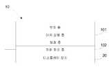
도 1에는 선행기술의 터치 디스플레이(10)의 구조가 도시되어 있으며, 상기 터치 디스플레이(10)에서는 터치 감응 층(101) 및 디스플레이 장치(20) 상에 위치해 있는 차폐 회로 층(102)이 서로 절연되어 있으며, 상기 차폐 회로 층(102)은 접지되어 있다.1 shows a structure of a
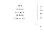
도 2에 도시된 바와 같이, 본 발명의 한 실시예에 의해 제공된 터치 디스플레이(30)는 디스플레이 장치(20) 및 터치 장치(터치 검출 장치)(11)를 포함한다. 도 3에 도시된 바와 같이, 상기 터치 장치(11)는 상기 디스플레이 장치(20) 상에 위치해 있는데, 다시 말하면 상기 터치 장치(11)는 상기 디스플레이 장치(20)의 디스플레이 표면 측 상에 위치해 있다. 상기 터치 장치(11)는 터치 감응 층(101)을 포함하며, 상기 터치 감응 층(101) 및 상기 디스플레이 장치(20) 사이에는 차폐 회로 층(102)이 배치되어 있다. 상기 터치 감응 층(101) 및 상기 차폐 회로 층(102) 사이에는 투명한 절연 층(103)이 배치되어 있으며, 상기 차폐 회로 층(102)과 상기 터치 감응 층(101)은 등전위(equipotential)를 이룬다. 상기 터치 감응 층(101)이 스크래치되는 것을 방지하기 위해 상기 터치 감응 층(101) 상에 (도 2에 도시되지 않은) 보호 층이 배치될 수 있다.2, the
한 실시예에서는, 등전위를 이루는 상기 차폐 회로 층(102) 및 상기 터치 감응 층(101)이 상기 터치 감응 층(101)과 상기 차폐 회로 층(102)을 전기적으로 접속함으로써 이루어질 수 있다. 예를 들면, 상기 차폐 회로 층(102) 및 상기 터치 감응 층(101)은 상기 투명한 절연 층(103)을 관통하는 비어(via)에 의해 서로 전기적으로 접속될 수 있다.In one embodiment, the
이러한 경우에, 상기 터치 디스플레이의 차폐 회로 층은 접지되어 있지 않으며, 상기 차폐 회로 층과 상기 터치 감응 층 간의 전위 차가 없이 상기 차폐 회로 층이 상기 터치 감응 층과의 등전위를 이루고 있기 때문에, 상기 터치 감응 층 및 상기 차폐 회로 층 간의 결합 정전용량의 형성이 회피되며 상기 터치 감응 층이 정상적으로 작동할 수 있게 된다.In this case, since the shielding circuit layer of the touch display is not grounded and the shielding circuit layer has an equal potential with the touch sensing layer without a potential difference between the shielding circuit layer and the touch sensing layer, Layer and the shielding circuit layer is avoided and the touch sensitive layer can be normally operated.
한 실시예에서는, 상기 터치 감응 층 및 상기 차폐 회로 층이 투명한 도전 층들일 수 있다. 그러므로, 상기 디스플레이 장치상에 나타나 있는 정보가 상기 터치 감응 층 및 상기 차폐 회로 층을 통해 보일 수 있다. 예를 들면, 상기 투명한 도전 층은 산화 인듐 주석(Indium Tin Oxide; ITO) 층, 산화 인듐 아연(Indium Zinc Oxide; IZO) 층 등과 같은 금속 산화물 층일 수 있다.In one embodiment, the touch sensitive layer and the shielding circuit layer may be transparent conductive layers. Therefore, information displayed on the display device can be viewed through the touch sensitive layer and the shielding circuit layer. For example, the transparent conductive layer may be a metal oxide layer such as an indium tin oxide (ITO) layer, an indium zinc oxide (IZO) layer, or the like.
도 4에 도시된 바와 같이, 한 실시예에서는, 상기 디스플레이 장치(20)가 어레이 기판(202) 및 카운터 기판(201)을 포함할 수 있으며, 상기 터치 감응 층(101), 상기 차폐 회로 층(102) 및 상기 투명한 절연 층(103)은 상기 카운터 기판(201) 상에 배치된다. 예를 들면, 상기 디스플레이 장치(20)는 액정 디스플레이 패널, 유기 발광 다이오드(Organic Lighting Emitting Diode; OLED) 디스플레이 패널, 또는 임의 타입의 다른 적합한 디스플레이 패널일 수 있다. 상기 디스플레이 장치(20)가 액정 디스플레이 패널인 경우에, 상기 카운터 기판(201)은 컬러 필터 기판일 수 있다.4, in one embodiment, the
도 5에 도시된 바와 같이, 한 실시예에서는, 상기 터치 디스플레이(30)가 전압 공급부(301)를 부가적으로 포함할 수 있으며, 상기 전압 공급부(301)는 상기 차폐 회로 층 및 상기 터치 감응 층에 대해 동일한 전압을 공급하기 위해 상기 차폐 회로 층 및 (도 5에 도시되지 않은) 상기 터치 장치(11)의 터치 감응 층과 접속된다.5, in one embodiment, the
상기 전압 공급부는 상기 터치 디스플레이의 차폐 회로 층 및 터치 감응 층에 대해 동일한 전압을 공급하며, 이러한 경우에 상기 차폐 회로 층은 접지되어 있지 않고, 상기 차폐 회로 층 및 상기 터치 감응 층 간의 전위 차가 없이 상기 터치 감응 층과 동일한 전압으로 상기 차폐 회로 층에 부하가 걸리게 됨으로써, 상기 터치 디스플레이의 차폐 회로 층 및 터치 감응 층 간의 결합 정전용량의 형성이 회피되고 상기 터치 감응 층이 정상적으로 작동할 수 있게 된다.Wherein the voltage supply unit supplies the same voltage to the shielding circuit layer and the touch sensitive layer of the touch display, in which case the shielding circuit layer is not grounded, and the voltage difference between the shielding circuit layer and the touch sensitive layer A load is applied to the shielding circuit layer with the same voltage as that of the touch sensitive layer so that formation of the coupling capacitance between the shielding circuit layer and the touch sensitive layer of the touch display is avoided and the touch sensitive layer can be normally operated.
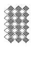
상기 터치 감응 층(101) 외에도, 위에서 언급된 터치 디스플레이의 터치 장치(11)는 또한 다른 어떤 적합한 구성요소들을 포함할 수 있다. 상기 터치 감응 층(101)에는 또한 어느 공지된 구조가 채용될 수 있다. 예를 들면, 상기 터치 감응 층(101)은 도 6에 도시된 구조를 지닐 수 있다. 도 6에 도시된 바와 같이, 상기 터치 감응 층(101)은 회색(gray)으로 채워져 있는 마름모꼴(diamond)들로 나타나 있는 제1 감응 패턴들 및 백색으로 채워져 있는 마름모꼴들로 나타나 있는 제2 감응 패턴들로 이루어져 있다. 상기 제1 감응 패턴들은 열(column) 방향을 따른 접속 라인들에 의해 서로 접속되어 있으며, 상기 제2 감응 패턴들은 행(row) 방향을 따른 접속 라인들에 의해 서로 접속되어 있다. 더욱이, 비록 상기 도면들에서 상기 제1 감응 패턴들의 접속 라인들 및 상기 제2 감응 패턴들의 접속 라인들이 서로 교차되어 있는 것처럼 보인다 하더라도, 상기 제1 감응 패턴들의 접속 라인들 및 상기 제2 감응 패턴들의 접속 라인들이 실제로는 전기적으로 절연되어 있다. 그러므로, 터치 지점은 행 방향을 따른 상기 감응 패턴들의 정전용량 변화 및 열 방향을 따른 상기 감응 패턴들의 정전용량 변화를 검출함으로써 결정될 수 있다. 그러나, 위에서 언급된 특정 구조는 단지 전형적인 구조일 뿐이며, 본 발명의 실시예들에 따른 터치 감응 층은 어느 적합한 구조를 지닐 수 있다.In addition to the touch
그 외에도, 본 발명은 본 발명의 어느 한 실시예에에 따른 터치 디스플레이를 포함하는 전자 장치를 제공한다. 예를 들면, 상기 전자 장치는 이동 전화, 태블릿 컴퓨터, 디지털 스틸 카메라, 비디오 카메라, 네비게이터 등일 수 있다.In addition, the present invention provides an electronic device comprising a touch display according to any one of the embodiments of the present invention. For example, the electronic device may be a mobile phone, a tablet computer, a digital still camera, a video camera, a navigator, and the like.
상기 전자 장치에서는, 상기 터치 디스플레이의 터치 감응 층 및 차폐 회로 층이 등전위를 이루고 있기 때문에, 상기 터치 디스플레이의 차폐 회로 층 및 터치 감응 층 간의 결합 정전용량의 형성이 회피되고 상기 터치 감응 층이 정상적으로 작동할 수 있게 된다.In the electronic device, since the touch sensitive layer and the shielding circuit layer of the touch display have the same potential, the formation of the coupled electrostatic capacitance between the shielding circuit layer and the touch sensitive layer of the touch display is avoided and the touch sensitive layer is normally operated .
위에서 언급된 실시예들의 설명에 의하면, 본 발명의 실시예들은 적어도 다음과 같은 구조를 제공할 수 있다.According to the description of the above-mentioned embodiments, embodiments of the present invention can provide at least the following structure.
(1) 터치 디스플레이로서,(1) As a touch display,
상기 터치 디스플레이는, The touch display includes:
디스플레이 장치; A display device;
상기 디스플레이 장치의 디스플레이 표면 측 상에 위치해 있는 터치 장치로서, 터치 감응 층을 포함하는 터치 장치; A touch device positioned on a display surface side of the display device, comprising: a touch device including a touch sensitive layer;
상기 터치 감응 층 및 상기 디스플레이 장치 사이에 배치된 차폐 회로 층; 및 A shielding circuit layer disposed between the touch sensitive layer and the display device; And
상기 터치 감응 층 및 상기 차폐 회로 층 사이에 배치된 투명한 절연 층; A transparent insulating layer disposed between the touch sensitive layer and the shielding circuit layer;
을 포함하며, / RTI >
상기 차폐 회로 층 및 상기 터치 감응 층은 등전위를 이루는, 터치 디스플레이. Wherein the shielding circuit layer and the touch sensitive layer have an equal potential.
(2) (1) 항목에 있어서, 상기 차폐 회로 층 및 상기 터치 감응 층은 서로 전기적으로 접속되어 있는, 터치 디스플레이. (2) The touch display according to item (1), wherein the shielding circuit layer and the touch sensitive layer are electrically connected to each other.
(3) (1) 또는 (2) 항목에 있어서, 상기 터치 감응 층 및 상기 차폐 회로 층은 투명한 도전 층들인, 터치 디스플레이. (3) The touch display according to (1) or (2), wherein the touch sensitive layer and the shielding circuit layer are transparent conductive layers.
(4) (1) 내지 (3) 항목 중 어느 한 항목에 있어서, 상기 투명한 도전 층들은 산화 인듐 주석 층들 또는 산화 인듐 아연 층들인, 터치 디스플레이. (4) The touch display according to any one of items (1) to (3), wherein the transparent conductive layers are indium tin oxide layers or indium zinc oxide layers.
(5) (1) 내지 (4) 항목 중 어느 한 항목에 있어서, 상기 디스플레이 장치는 카운터 기판 및 어레이 기판을 포함하며, 상기 터치 감응 층, 상기 차폐 회로 층 및 상기 투명한 절연 층은 상기 카운터 기판상에 배치되는, 터치 디스플레이. (5) In any one of items (1) to (4), the display device includes a counter substrate and an array substrate, and the touch sensitive layer, the shielding circuit layer, And a touch display.
(6) (1) 내지 (5) 항목 중 어느 한 항목에 있어서, 상기 디스플레이 장치는 액정 디스플레이 패널이며 상기 카운터 기판은 컬러 필터 기판인, 터치 디스플레이. (6) The touch display according to any one of items (1) to (5), wherein the display device is a liquid crystal display panel and the counter substrate is a color filter substrate.
(7) (1) 내지 (6) 항목 중 어느 한 항목에 있어서, (7) In any one of items (1) to (6)
상기 차폐 회로 층 및 상기 터치 감응 층에 대해 동일한 전압을 공급하기 위해 상기 차폐 회로 층 및 상기 터치 감응 층과 접속되는 전압 공급부; A voltage supplier connected to the shielding circuit layer and the touch sensitive layer to supply the same voltage to the shielding circuit layer and the touch sensitive layer;
를 부가적으로 포함하는, 터치 디스플레이. The touch display further comprising:
(8) (1) 내지 (7) 항목 중 어느 한 항목에 따른 터치 디스플레이를 포함하는 전자 장치. (8) An electronic device comprising a touch display according to any one of items (1) to (7).
위에 언급한 설명은 본 발명의 보호 범위를 한정하기보다는 오히려 단지 본 발명의 특정 구현예일 뿐이며 본 발명에 의해 개시되는 기술적 범위 내에서 당업자에 의해 용이하게 예측될 수 있는 어떠한 변경 또는 교체는 본 발명의 보호 범위에 속하는 것이다. 따라서, 본 발명의 보호 범위는 첨부된 청구항들에서 한정된다.It is to be understood that the above description is only a specific embodiment of the invention rather than limiting the scope of the invention and that any changes or substitutions that may readily be anticipated by one skilled in the art within the scope of the invention disclosed by the present invention, It is in the scope of protection. Accordingly, the protection scope of the present invention is defined in the appended claims.
Claims (8)
Translated fromKorean상기 터치 디스플레이는,
디스플레이 장치;
상기 디스플레이 장치의 디스플레이 표면 측 상에 위치해 있는 터치 장치로서, 터치 감응 층을 포함하는 터치 장치;
상기 터치 감응 층 및 상기 디스플레이 장치 사이에 배치된 차폐 회로 층; 및
상기 터치 감응 층 및 상기 차폐 회로 층 사이에 배치된 투명한 절연 층;
을 포함하며,
상기 차폐 회로 층과 상기 터치 감응 층은 등전위를 이루는, 터치 디스플레이.As a touch display,
The touch display includes:
A display device;
A touch device positioned on a display surface side of the display device, comprising: a touch device including a touch sensitive layer;
A shielding circuit layer disposed between the touch sensitive layer and the display device; And
A transparent insulating layer disposed between the touch sensitive layer and the shielding circuit layer;
/ RTI >
Wherein the shielding circuit layer and the touch sensitive layer have an equal potential.
상기 차폐 회로 층 및 상기 터치 감응 층에 대해 동일한 전압을 공급하기 위해 상기 차폐 회로 층 및 상기 터치 감응 층과 접속되어 있는 전압 공급부;
를 부가적으로 포함하는, 터치 디스플레이.3. The method according to claim 1 or 2,
A voltage supplier connected to the shielding circuit layer and the touch sensitive layer to supply the same voltage to the shielding circuit layer and the touch sensitive layer;
The touch display further comprising:
Applications Claiming Priority (3)
| Application Number | Priority Date | Filing Date | Title |
|---|---|---|---|
| CN201120548632.3 | 2011-12-23 | ||
| CN2011205486323UCN202372727U (en) | 2011-12-23 | 2011-12-23 | Touch display |
| PCT/CN2012/082788WO2013091431A1 (en) | 2011-12-23 | 2012-10-11 | Touch display and electronic device |
Publications (2)
| Publication Number | Publication Date |
|---|---|
| KR20130084976A KR20130084976A (en) | 2013-07-26 |
| KR101539258B1true KR101539258B1 (en) | 2015-07-24 |
Family
ID=46596424
Family Applications (1)
| Application Number | Title | Priority Date | Filing Date |
|---|---|---|---|
| KR1020127030635AActiveKR101539258B1 (en) | 2011-12-23 | 2012-10-11 | Touch display and electronic apparatus |
Country Status (5)
| Country | Link |
|---|---|
| EP (1) | EP2808727A4 (en) |
| JP (1) | JP2015501055A (en) |
| KR (1) | KR101539258B1 (en) |
| CN (1) | CN202372727U (en) |
| WO (1) | WO2013091431A1 (en) |
Families Citing this family (6)
| Publication number | Priority date | Publication date | Assignee | Title |
|---|---|---|---|---|
| CN202372727U (en)* | 2011-12-23 | 2012-08-08 | 京东方科技集团股份有限公司 | Touch display |
| US9250726B2 (en) | 2011-12-23 | 2016-02-02 | Boe Technology Group Co., Ltd. | Touch display and electronic apparatus |
| CN103399678A (en)* | 2013-08-02 | 2013-11-20 | 敦泰科技有限公司 | Self-capacitance touch screen and touch display device |
| KR102183655B1 (en)* | 2014-01-28 | 2020-11-27 | 삼성디스플레이 주식회사 | Display apparatus |
| KR102350084B1 (en)* | 2015-01-15 | 2022-01-11 | 삼성디스플레이 주식회사 | Touch panel and display device using the same |
| CN106249979B (en)* | 2016-08-31 | 2019-05-31 | 京东方科技集团股份有限公司 | Touch electrode structure and touch control display apparatus |
Citations (2)
| Publication number | Priority date | Publication date | Assignee | Title |
|---|---|---|---|---|
| US20110007021A1 (en)* | 2009-07-10 | 2011-01-13 | Jeffrey Traer Bernstein | Touch and hover sensing |
| US20110080373A1 (en)* | 2009-10-07 | 2011-04-07 | Wintek Corporation | Touch Panel and Display Device Using the Same |
Family Cites Families (7)
| Publication number | Priority date | Publication date | Assignee | Title |
|---|---|---|---|---|
| JP5051690B2 (en)* | 2007-01-30 | 2012-10-17 | 株式会社ジャパンディスプレイウェスト | Display device with input function |
| GB2456312A (en)* | 2008-01-10 | 2009-07-15 | Young Fast Optoelectronics Co | Transparent Capacitive Touch Panel |
| JP2009175784A (en)* | 2008-01-21 | 2009-08-06 | Mitsubishi Electric Corp | Touch panel device |
| CN201352340Y (en)* | 2008-12-26 | 2009-11-25 | 升达科技股份有限公司 | Display device of touch panel |
| JP2011186623A (en)* | 2010-03-05 | 2011-09-22 | Hitachi Displays Ltd | Display device with touch panel |
| JP5370945B2 (en)* | 2010-03-19 | 2013-12-18 | 株式会社ジャパンディスプレイ | Electro-optical device with touch panel and input function |
| CN202372727U (en)* | 2011-12-23 | 2012-08-08 | 京东方科技集团股份有限公司 | Touch display |
- 2011
- 2011-12-23CNCN2011205486323Upatent/CN202372727U/ennot_activeExpired - Lifetime
- 2012
- 2012-10-11JPJP2014547680Apatent/JP2015501055A/enactivePending
- 2012-10-11KRKR1020127030635Apatent/KR101539258B1/enactiveActive
- 2012-10-11WOPCT/CN2012/082788patent/WO2013091431A1/enactiveApplication Filing
- 2012-10-11EPEP12791674.0Apatent/EP2808727A4/ennot_activeCeased
Patent Citations (2)
| Publication number | Priority date | Publication date | Assignee | Title |
|---|---|---|---|---|
| US20110007021A1 (en)* | 2009-07-10 | 2011-01-13 | Jeffrey Traer Bernstein | Touch and hover sensing |
| US20110080373A1 (en)* | 2009-10-07 | 2011-04-07 | Wintek Corporation | Touch Panel and Display Device Using the Same |
Also Published As
| Publication number | Publication date |
|---|---|
| EP2808727A4 (en) | 2015-08-05 |
| JP2015501055A (en) | 2015-01-08 |
| WO2013091431A1 (en) | 2013-06-27 |
| CN202372727U (en) | 2012-08-08 |
| KR20130084976A (en) | 2013-07-26 |
| EP2808727A1 (en) | 2014-12-03 |
Similar Documents
| Publication | Publication Date | Title |
|---|---|---|
| US11378833B2 (en) | Display apparatus and input device | |
| US10459555B2 (en) | In-cell touch panel, driving method thereof and display device | |
| US10175803B2 (en) | Touch sensing device and method for driving the same | |
| US9250726B2 (en) | Touch display and electronic apparatus | |
| KR102228561B1 (en) | Display device indlucing touch sensor | |
| US9207819B2 (en) | Touch sensing display panel and touch sensing liquid crystal display panel | |
| KR101386327B1 (en) | Display device equipped with touch panel | |
| KR101452042B1 (en) | Touch screen panel and touch screen apparatus | |
| US9086766B2 (en) | Touch panel and touch display panel | |
| KR101539258B1 (en) | Touch display and electronic apparatus | |
| US9496097B2 (en) | Touch window having improved electrode pattern structure | |
| JP2010507166A (en) | Electronic device and touch panel arrangement method thereof | |
| JP2011128673A (en) | Electrostatic capacitance-type input device, method of testing electrostatic capacitance-type input device, and driving device for electrostatic capacitance-type input device | |
| CN104615323A (en) | Three-dimensional module, three-dimensional display device and drive method of three-dimensional module | |
| KR102231934B1 (en) | DISPLAY DEVICE WITH INTEGRATED TOUCH SCREEN AND Method for Manufacturing | |
| JP2013148952A (en) | Detector, display and electronic apparatus | |
| KR101318446B1 (en) | Electrostatic capacitive type touch-sensitive panel for display device | |
| TWI518571B (en) | Touch device and driving method thereof | |
| US20140340598A1 (en) | Touch panel | |
| KR101675254B1 (en) | Display device integrated with touch screen | |
| US9411448B2 (en) | Touch display apparatus | |
| KR102841773B1 (en) | Touch panel, display device having thereof and detecting touch | |
| JP2012230471A (en) | Touch panel | |
| CN106354309B (en) | Touch panel and display device | |
| KR20190045704A (en) | Touch Panel |
Legal Events
| Date | Code | Title | Description |
|---|---|---|---|
| PA0105 | International application | Patent event date:20121122 Patent event code:PA01051R01D Comment text:International Patent Application | |
| A201 | Request for examination | ||
| PA0201 | Request for examination | Patent event code:PA02012R01D Patent event date:20121130 Comment text:Request for Examination of Application | |
| PG1501 | Laying open of application | ||
| E902 | Notification of reason for refusal | ||
| PE0902 | Notice of grounds for rejection | Comment text:Notification of reason for refusal Patent event date:20140430 Patent event code:PE09021S01D | |
| E902 | Notification of reason for refusal | ||
| PE0902 | Notice of grounds for rejection | Comment text:Notification of reason for refusal Patent event date:20141031 Patent event code:PE09021S01D | |
| E701 | Decision to grant or registration of patent right | ||
| PE0701 | Decision of registration | Patent event code:PE07011S01D Comment text:Decision to Grant Registration Patent event date:20150430 | |
| GRNT | Written decision to grant | ||
| PR0701 | Registration of establishment | Comment text:Registration of Establishment Patent event date:20150720 Patent event code:PR07011E01D | |
| PR1002 | Payment of registration fee | Payment date:20150721 End annual number:3 Start annual number:1 | |
| PG1601 | Publication of registration | ||
| FPAY | Annual fee payment | Payment date:20180628 Year of fee payment:4 | |
| PR1001 | Payment of annual fee | Payment date:20180628 Start annual number:4 End annual number:4 | |
| FPAY | Annual fee payment | Payment date:20190627 Year of fee payment:5 | |
| PR1001 | Payment of annual fee | Payment date:20190627 Start annual number:5 End annual number:5 | |
| PR1001 | Payment of annual fee | Payment date:20200701 Start annual number:6 End annual number:6 | |
| PR1001 | Payment of annual fee | Payment date:20210617 Start annual number:7 End annual number:7 | |
| PR1001 | Payment of annual fee | Payment date:20220623 Start annual number:8 End annual number:8 | |
| PR1001 | Payment of annual fee | Payment date:20240619 Start annual number:10 End annual number:10 | |
| PR1001 | Payment of annual fee | Payment date:20250616 Start annual number:11 End annual number:11 |