KR101538982B1 - High molecular weight alkyl-allyl cobalttricarbonyl complexes and use thereof for preparing dielectric thin films - Google Patents
High molecular weight alkyl-allyl cobalttricarbonyl complexes and use thereof for preparing dielectric thin filmsDownload PDFInfo
- Publication number
- KR101538982B1 KR101538982B1KR1020127006060AKR20127006060AKR101538982B1KR 101538982 B1KR101538982 B1KR 101538982B1KR 1020127006060 AKR1020127006060 AKR 1020127006060AKR 20127006060 AKR20127006060 AKR 20127006060AKR 101538982 B1KR101538982 B1KR 101538982B1
- Authority
- KR
- South Korea
- Prior art keywords
- allyl
- deposition
- precursor
- film
- cobalt
- Prior art date
- Legal status (The legal status is an assumption and is not a legal conclusion. Google has not performed a legal analysis and makes no representation as to the accuracy of the status listed.)
- Active
Links
Images


Classifications
- C—CHEMISTRY; METALLURGY
- C07—ORGANIC CHEMISTRY
- C07F—ACYCLIC, CARBOCYCLIC OR HETEROCYCLIC COMPOUNDS CONTAINING ELEMENTS OTHER THAN CARBON, HYDROGEN, HALOGEN, OXYGEN, NITROGEN, SULFUR, SELENIUM OR TELLURIUM
- C07F15/00—Compounds containing elements of Groups 8, 9, 10 or 18 of the Periodic Table
- C07F15/06—Cobalt compounds
- C—CHEMISTRY; METALLURGY
- C23—COATING METALLIC MATERIAL; COATING MATERIAL WITH METALLIC MATERIAL; CHEMICAL SURFACE TREATMENT; DIFFUSION TREATMENT OF METALLIC MATERIAL; COATING BY VACUUM EVAPORATION, BY SPUTTERING, BY ION IMPLANTATION OR BY CHEMICAL VAPOUR DEPOSITION, IN GENERAL; INHIBITING CORROSION OF METALLIC MATERIAL OR INCRUSTATION IN GENERAL
- C23C—COATING METALLIC MATERIAL; COATING MATERIAL WITH METALLIC MATERIAL; SURFACE TREATMENT OF METALLIC MATERIAL BY DIFFUSION INTO THE SURFACE, BY CHEMICAL CONVERSION OR SUBSTITUTION; COATING BY VACUUM EVAPORATION, BY SPUTTERING, BY ION IMPLANTATION OR BY CHEMICAL VAPOUR DEPOSITION, IN GENERAL
- C23C16/00—Chemical coating by decomposition of gaseous compounds, without leaving reaction products of surface material in the coating, i.e. chemical vapour deposition [CVD] processes
- C23C16/22—Chemical coating by decomposition of gaseous compounds, without leaving reaction products of surface material in the coating, i.e. chemical vapour deposition [CVD] processes characterised by the deposition of inorganic material, other than metallic material
- C23C16/30—Deposition of compounds, mixtures or solid solutions, e.g. borides, carbides, nitrides
- C23C16/40—Oxides
- C23C16/406—Oxides of iron group metals
- C—CHEMISTRY; METALLURGY
- C23—COATING METALLIC MATERIAL; COATING MATERIAL WITH METALLIC MATERIAL; CHEMICAL SURFACE TREATMENT; DIFFUSION TREATMENT OF METALLIC MATERIAL; COATING BY VACUUM EVAPORATION, BY SPUTTERING, BY ION IMPLANTATION OR BY CHEMICAL VAPOUR DEPOSITION, IN GENERAL; INHIBITING CORROSION OF METALLIC MATERIAL OR INCRUSTATION IN GENERAL
- C23C—COATING METALLIC MATERIAL; COATING MATERIAL WITH METALLIC MATERIAL; SURFACE TREATMENT OF METALLIC MATERIAL BY DIFFUSION INTO THE SURFACE, BY CHEMICAL CONVERSION OR SUBSTITUTION; COATING BY VACUUM EVAPORATION, BY SPUTTERING, BY ION IMPLANTATION OR BY CHEMICAL VAPOUR DEPOSITION, IN GENERAL
- C23C16/00—Chemical coating by decomposition of gaseous compounds, without leaving reaction products of surface material in the coating, i.e. chemical vapour deposition [CVD] processes
- C23C16/44—Chemical coating by decomposition of gaseous compounds, without leaving reaction products of surface material in the coating, i.e. chemical vapour deposition [CVD] processes characterised by the method of coating
- C23C16/455—Chemical coating by decomposition of gaseous compounds, without leaving reaction products of surface material in the coating, i.e. chemical vapour deposition [CVD] processes characterised by the method of coating characterised by the method used for introducing gases into reaction chamber or for modifying gas flows in reaction chamber
- C23C16/45523—Pulsed gas flow or change of composition over time
- C23C16/45525—Atomic layer deposition [ALD]
- C23C16/45553—Atomic layer deposition [ALD] characterized by the use of precursors specially adapted for ALD
Landscapes
- Chemical & Material Sciences (AREA)
- Organic Chemistry (AREA)
- Metallurgy (AREA)
- Engineering & Computer Science (AREA)
- Materials Engineering (AREA)
- Mechanical Engineering (AREA)
- Chemical Kinetics & Catalysis (AREA)
- General Chemical & Material Sciences (AREA)
- Inorganic Chemistry (AREA)
- Chemical Vapour Deposition (AREA)
- Electrodes Of Semiconductors (AREA)
- Formation Of Insulating Films (AREA)
- Insulated Gate Type Field-Effect Transistor (AREA)
- Physical Vapour Deposition (AREA)
Abstract
Translated fromKorean
Description
Translated fromKorean관련 출원의 교차 참조Cross reference of related application
본 출원은 2009년 8월 7일 출원된 미국 가출원 제61/232,219호 및 2010년 2월 4일 출원된 미국 가출원 제61/301,390호에 대한 우선권을 주장한다. 각각의 상기 미국 가출원의 개시 내용은 원용에 의해 전체로서 본 명세서에 통합된다.This application claims priority to U.S. Provisional Application No. 61 / 232,219, filed on August 7, 2009, and U.S. Provisional Application No. 61 / 301,390, filed February 4, 2010. The disclosure of each of which is incorporated herein by reference in its entirety.
기술 분야Technical field
본 발명은, 고분자량의 알킬-알릴 코발트트리카르보닐 착체와, 이러한 착체를 사용하여 화학 증착 (CVD) 또는 원자막 퇴적 (ALD)에 의해 유전체 박막을 제조하는 방법에 관한 것이다.The present invention relates to a high molecular weight alkyl-allyl cobalt tricarbonyl complex and a method for producing a dielectric thin film by chemical vapor deposition (CVD) or atomic layer deposition (ALD) using such a complex.
다양한 유기 금속성 전구체가 고유전율(high κ) 유전체(dielectric) 금속 박막을 형성하기 위해 사용되고 있다. 다양한 기술들이 박막의 퇴적을 위해 사용되고 있다. 이들은 반응성 스퍼터링, 이온 보조형 퇴적, 졸-겔 퇴적, CVD, 및 원자막 에피택시로도 알려져 있는 ALD를 포함한다. CVD와 ALD 공정은, 우수한 조성 제어성, 높은 필름 균일성, 도핑에 대한 양호한 제어성의 장점으로 인해, 그리고 고도로 비평탄(non-planar)한 미소 전자장치 기하에 대하여 월등한 등각형 스텝 커버리지(conformal step coverage)를 제공하기 때문에, 그 사용이 점차 증가하고 있는 추세이다.Various organometallic precursors have been used to form high k dielectric metal films. Various techniques are being used to deposit thin films. These include reactive sputtering, ion-assisted deposition, sol-gel deposition, CVD, and ALD, also known as atomic film epitaxy. The CVD and ALD processes are advantageous because of the advantages of good composition control, high film uniformity, good controllability for doping, and superior uniformity of step coverage for highly non-planar microelectronic geometries. step coverage, and its use is gradually increasing.
(금속유기 CVD 또는 MOCVD라고도 불리우는) CVD 는 일종의 화학 공정으로서, 전구체를 사용하여 기재 상에 박막을 형성한다. 통상의 CVD 공정에서 전구체는 저압 또는 주변 압력 반응 체임버 내에서 기재(웨이퍼) 상으로 통과된다. 전구체는 기재 표면에서 반응하고/하거나 분해되어 퇴적 물질의 박막을 생성한다. 휘발성 부산물은 반응 체임버를 관통하는 가스 흐름에 의해 제거된다. 퇴적되는 막 두께를 제어하기는 매우 어려운데, 이는 상기 막 두께가 온도, 압력, 가스 흐름 부피 및 균일성, 화학적 고갈 효과 및 시간 등에 따라 달라지기 때문이다.CVD (also called metal organic CVD or MOCVD) is a kind of chemical process that uses a precursor to form a thin film on a substrate. In a typical CVD process, the precursor is passed over a substrate (wafer) in a low pressure or ambient pressure reaction chamber. The precursor reacts and / or decomposes on the substrate surface to produce a thin film of deposited material. Volatile byproducts are removed by the gas flow through the reaction chamber. It is very difficult to control the deposited film thickness because the film thickness depends on temperature, pressure, gas flow volume and uniformity, chemical depletion effect and time.
ALD는 박막의 퇴적을 위한 공지된 방법이다. 이는, 자기 한정적이고, 시계열적이며, 표면 반응에 기초한 독특한 필름 성장 기술로서, 원자막 형성제어가 가능하고 다양한 조성의 기재 상으로 전구체에 의해 제공된 물질의 퇴적-등각(deposit-conformal) 박막을 제공할 수 있다. ALD의 경우, 전구체는 반응 중에 분리된다. 제1 전구체는 기재 위로 지나가면서 기재 표면에 단층을 생산한다. 반응하지 않은 과량의 전구체는 모두 반응 체임버 밖으로 펌핑되어 나간다. 이어서, 제2 전구체가 기재 위로 지나가면서 제1 전구체와 반응함으로써 기재 상에 첫번째로 형성된 단층 필름 상에 제2 단층 필름을 형성한다. 이러한 사이클을 반복하여 소망하는 두께를 가진 필름을 생성한다. ALD 필름 성장은 자기 한정적이고, 표면 반응을 기반으로 하여, 나노미터 두께 규모로 제어될 수 있는 균일한 퇴적물을 생성한다.ALD is a known method for depositing thin films. This is a unique film growth technique that is self-limiting, time-wise, and based on surface reactions, providing a deposit-conformal film of material provided by a precursor on a substrate of various compositions, can do. In the case of ALD, the precursor is separated during the reaction. The first precursor passes over the substrate and produces a monolayer on the substrate surface. Any excess unreacted precursor is pumped out of the reaction chamber. The second precursor then reacts with the first precursor as it passes over the substrate to form a second monolayer film on the first formed monolayer film on the substrate. This cycle is repeated to produce a film having the desired thickness. ALD film growth is self-limiting, and based on surface reactions, produces uniform sediments that can be controlled on a nanometer-scale scale.
유전체 박막은, 반도체 장치의 제작과 나노기술 등 다양한 중요 응용 분야를 가진다. 이러한 응용 분야로서는 고굴절률 광학 코팅, 부식 보호 코팅, 광촉매성 자체 세정 유리 코팅, 생체 적합성 코팅, 유전체 커패시터 층, 및 FET (전계 효과 트랜지스터) 내의 게이트 유전체 절연 필름, 커패시터 전극, 게이트 전극, 접착성 확산 배리어 및 집적 회로를 예로 들 수 있다. 유전체 박막은 또한, 다이나믹 랜덤 액세스 메모리(DRAM) 응용 분야를 위한 고유전율 유전체 산화물, 및 적외선 감지기에서 사용되는 강유전성 페로브스카이트와 비휘발성 강유전성 랜덤 액세스 메모리 (NV-FeRAM) 등 미소 전자 응용 분야에서 사용될 수 있다. 미소 전자 부품의 크기가 지속적으로 감소됨에 따라 이러한 유전체 박막의 사용에 대한 수요가 증가하고 있다.Dielectric thin films have various important applications such as semiconductor device fabrication and nanotechnology. Such applications include high refractive index optical coatings, corrosion protection coatings, photocatalytic self-cleaning glass coatings, biocompatible coatings, dielectric capacitor layers, and gate dielectric insulation films in FETs (field effect transistors), capacitor electrodes, gate electrodes, Barriers and integrated circuits are examples. Dielectric thin films have also been used in microelectronic applications such as high dielectric constant oxides for dynamic random access memory (DRAM) applications, ferroelectric perovskites for use in infrared detectors and non-volatile ferroelectric random access memory (NV-FeRAM) Can be used. As the size of microelectronic components is continuously reduced, there is an increasing demand for the use of such dielectric thin films.
Dickson R. 등은. [(η3-C3H5)Co(CO)3], [η3-C3H4Me)Co(CO)3] 및 [η3-C3H5Me2)Co(CO)3] 등 MOCVD 에서의 사용을 위한 코발트 착체를 보고한 바 있다.Polyhedron. 15(13):2237-2245 (1996).Dickson R. et al.[(η 3 -C 3 H 5 ) Co (CO) 3], [η 3 -C 3 H 4 Me) Co (CO) 3] and[η 3 -C 3 H 5 Me 2) Co (CO) 3 ] Have been reported for use in MOCVD.Polyhedron . 15 (13): 2237-2245 (1996).
Husebye S. 및 Jonassen H.도 코발트 착체를 보고한 바 있다.ActaChem. Scand. 18(7):1581-1585 (1964).Husebye S. and Jonassen H. also reported cobalt complexes.ActaChem. Scand . 18 (7): 1581-1585 (1964).
Pankayatselvan R. 및 Nicholas, K. 도 코발트 착체를 보고한 바 있다.J. Organomet.Chem. 384:361-380.Pankayatselvan R. and Nicholas, K. have also reported cobalt complexes.J. Organomet.Chem . 384: 361-380.
현재 CVD 및 ALD에서의 사용을 위한 전구체들은 반도체 등, 차세대 디바이스의 제조를 위한 새로운 공정을 수행하기에 요구되는 성능을 제공하지 못하고 있는 실정이다. 예컨대, 열 안정성의 향상, 휘발성의 증가, 증기압의 감소, 퇴적 속도의 증가 및 높은 유전율(permittivity)이 필요하다.Currently, precursors for use in CVD and ALD are not providing the performance required to perform new processes for the fabrication of next generation devices, such as semiconductors. For example, improvement of thermal stability, increase in volatility, decrease in vapor pressure, increase in deposition rate, and high permittivity are required.
발명의 개요Summary of the Invention
일구현예에서, 구조적으로 식 I에 해당하는 유기 금속성 전구체가 제공된다:In one embodiment, an organometallic precursor corresponding to formula I is provided structurally:

여기서, R1 은 C1-C8 알킬; R2 은 C3-C8 알킬; x 는 0, 1, 또는 2이고; y는 1이다.Wherein, R1 is C1 -C8 alkyl; R2 is C3 -C8 alkyl; x is 0, 1, or 2; y is 1.
다른 구현예에서, 구조적으로 식 I에 해당하되 R1은 C3-C8알킬이고; R2는 C1-C8 알킬이며; x 는 1 또는 2이고; y 는 0 또는 1인 유기 금속성 전구체가 제공된다.In other embodiments, but structurally corresponds to the formula I R1 is C3 -C8 Alkyl; R2 is C1 -C8 alkyl; x is 1 or 2; y is 0 or 1.
다른 구현예에서, 증착 공정을 통해 코발트 함유 박막을 형성하는 방법이 제공된다. 상기 방법은, 구조적으로 식 I에 해당하되 R1 및 R2 가 독립적으로 C2-C8알킬이고; x는 0, 1, 또는 2이고; y 는 0 또는 1이되, x 및 y가 둘 다 동시에 0이 될 수는 없는, 하나 이상의 전구체를 사용하는 것을 포함한다.In another embodiment, a method of forming a cobalt-containing thin film through a deposition process is provided. The method is structurally equivalent to formula I wherein R <1 > and R <2 > are independently C2 -C8 Alkyl; x is 0, 1, or 2; y is 0 or 1, with the proviso that x and y can not both be 0 at the same time.
위와 같이 요약한 구현예의 특별한 측면들을 비롯하여 다른 구현예들이 이어지는 상세한 설명으로부터 명확해질 것이다.Other implementations, including particular aspects of the above-summarized implementation, will become apparent from the following detailed description.
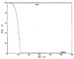
도 1은 (t-부틸)알릴Co(CO)3의 온도 대비 % 중량 감소를 나타내는, TGA (열중량 분석) 데이터를 그래프로 도시한 것이다.
도 2는, (네오펜틸)알릴Co(CO)3의 온도 대비 % 중량 감소를 나타내는, TGA 데이터를 그래프로 도시한 것이다.
도 3은, (네오펜틸)알릴Co(CO)3를 사용하여, 온도 대비 사이클 당 펄스형 CVD 성장(옹스트롱/사이클)을 그래프로 나타낸 것이다.
도 4는, (t-부틸)알릴Co(CO)3를 사용하여, 온도 대비 사이클 당 펄스형 CVD 성장(옹스트롱/사이클)을 그래프로 나타낸 것이다.
도 5는, 기재 온도 150℃로 ALD 성장을 수행함에 있어 (네오펜틸)알릴Co(CO)3 및 Me2NNH2를 사용하였을 경우, 사이클 횟수 vs. 두께(옹스트롱)를 그래프로 나타낸 것이다.
도 6은, 기재 온도 150℃로 ALD 성장을 수행함에 있어 (t-부틸)알릴Co(CO)3 및 Me2NNH2를 사용하였을 경우 사이클 횟수 vs. 두께(옹스트롱)를 그래프로 나타낸 것이다.Figure 1 graphically shows TGA (thermogravimetric analysis) data showing% weight loss versus temperature of (t-butyl) allyl Co (CO)3 .
Figure 2 is a graphical representation of TGA data showing% weight loss versus temperature for (neopentyl) allyl Co (CO)3 .
Figure 3 is a graphical representation of pulsed CVD growth per cycle versus temperature (Angstrom / cycle) using (neopentyl) allyl Co (CO)3 .
Figure 4 is a graphical representation of pulsed CVD growth per cycle versus temperature (Angstrom / cycle) using (t-butyl) allyl Co (CO)3 .
FIG. 5 is a graph showing the relationship between the (neopentyl) allyl CO (CO)3 and Me2 NNH2 in ALD growth at a substrate temperature of 150 ° C. The graph shows the thickness (Angstrong).
FIG. 6 is a graph showing changes in the number of cycles and the like when (t-butyl) allyl Co (CO)3 and Me2 NNH2 were used to perform ALD growth at a base temperature of 150 ° C. The graph shows the thickness (Angstrong).
본 발명의 다양한 측면에서, 치환된 알릴 유기 금속성 전구체, 이러한 전구체를 만들기 위한 방법, 및 이러한 전구체를 사용하여 금속, 금속-산화물 또는 금속 질화물 필름 등의 (그러나 이에 제한되지는 않는) 얇은 금속 함유 필름을 형성하는 방법이 제공된다.In various aspects of the invention, substituted allyl organometallic precursors, methods for making such precursors, and using such precursors to form thin metal-containing films, such as but not limited to metals, metal-oxide or metal nitride films, Is provided.
본 발명의 방법은 높은 유전상수를 나타내는 금속함유 박막을 생성하거나 성장시키기 위해 사용된다. 여기서 사용된 바의 유전체 박막이라는 용어는, 높은 유전율(permittivity)을 가지는 얇은 필름을 지칭한다.The method of the present invention is used to produce or grow metal-containing thin films exhibiting high dielectric constants. The term dielectric film as used herein refers to a thin film having a high permittivity.
여기서 사용된 바의, "고유전율(high κ) 유전체"라는 용어는 (유전 상수값이 대략 3.7인) 이산화규소와 비교할 때 더 높은 유전 상수(κ)를 가지는 재료, 예를 들어, 금속 함유 필름을 지칭한다. 통상, 고유전율 유전체 필름은 반도체 제조 공정에서 이산화규소 게이트 유전체를 대체하기 위해 사용된다. 유전체 필름이 게이트 재료로서 사용되며 최소한 이산화규소보다 더 높은 유전 상수를 가지는 경우, 고유전율 유전체 필름은 "고유전율 게이트 물성"을 가진다고 할 수 있다.As used herein, the term "high? Dielectric" refers to a material having a higher dielectric constant (?) Compared to silicon dioxide (dielectric constant value is about 3.7) Quot; Typically, high-k dielectric films are used to replace silicon dioxide gate dielectrics in semiconductor manufacturing processes. If the dielectric film is used as a gate material and has a dielectric constant at least higher than that of silicon dioxide, the high dielectric constant dielectric film can be said to have "high dielectric constant gate properties ".
여기서 사용된 바의 "상대 유전율" 이라는 용어는, 유전상수 (κ)와 같은 뜻을 가진다.The term "relative permittivity" as used herein has the same meaning as the dielectric constant (K).
여기서 사용된 바의, "전구체"라는 용어는, CVD 또는 ALD 등의 증착 공정에 의해 박막을 형성하도록 기재로 퇴적 또는 배달되는 유기 금속성 분자, 착체 및/또는 화합물을 지칭한다.As used herein, the term "precursor " refers to organometallic molecules, complexes and / or compounds deposited or delivered to a substrate to form a film by a CVD or ALD deposition process.
여기서 사용된 바의, "증착 공정" 이라는 용어는, CVD 또는 ALD 등 임의의 증착 기술을 지칭하기 위해 사용된다. 본 발명의 다양한 구현예에서, CVD는 전통적인 CVD, 액체 주입형 CVD, 또는 광보조형 CVD의 형태를 취할 수 있다. 다른 구현예에서, ALD는 전통적인 ALD, 액체 주입형 ALD, 광 보조형 ALD, 또는 플라즈마 보조형 ALD의 형태를 취할 수 있다.As used herein, the term "deposition process" is used to refer to any deposition technique, such as CVD or ALD. In various embodiments of the present invention, CVD may take the form of conventional CVD, liquid injection CVD, or photo-assisted CVD. In other embodiments, the ALD can take the form of conventional ALD, liquid injection ALD, light assisted ALD, or plasma assisted ALD.
본 발명의 치환된 알릴 유기금속 전구체는, 이전에 사용된 미치환의 전구체, 알릴Co(CO)3 보다 실질적으로 향상된 공급원이다. 미치환된 전구체, 알릴Co(CO)3 및 심지어, 메틸 및 디메틸 치환된 알릴Co(CO)3 전구체는 지나치게 휘발성이 강하여 CVD 공정에 혹은 반도체 응용 분야에서 제어된 얇은 층 퇴적에 별로 적합치 않다. 예를 들어, Dickson 등은 앞서 인용된 문헌 제2242면에서 "알릴성 수소를 메틸기로 대체하는 것은 증기압의 크기에 그다지 큰 영향을 주지 못한다"고 단언한 바 있다. 놀랍게도, 기대와 정반대로, 본 발명자들은 보다 벌키하게 치환된 알릴 전구체의 경우, 실상은, 증기압을 감소시키며, 따라서 그 취급이 보다 용이한 것을 확인하였다.The substituted allyl organometallic precursors of the present invention are a substantially improved source than the previously used unsubstituted precursor, allyl Co (CO)3 . Unsubstituted precursors, allyl Co (CO)3 and even methyl and dimethyl substituted allyl Co (CO)3 precursors are not very suitable for CVD processes or controlled thin layer deposition in semiconductor applications. For example, Dickson et al., In the previously cited document 2242, asserted that "replacing allylic hydrogens with methyl groups does not significantly affect the magnitude of the vapor pressure." Surprisingly, contrary to expectation, the present inventors have found that, in the case of a more bulky substituted allyl precursor, the actual phase reduces the vapor pressure and therefore is easier to handle.
또한, 이렇게 새로운 전구체들은 상이한 휘발성을 나타내어, 이들의 합성에 범용 용매를 사용할 수 있게 된다. 이는 보다 효율적인 분리를 가능케 하여, 전구체를 더 높은 순도로 분리하는 것을 용이하게 한다.In addition, these new precursors exhibit different volatilities, making it possible to use universal solvents for their synthesis. This allows for more efficient separation, facilitating the separation of the precursor into higher purity.
이들 전구체에 대한 목표로 하는 퇴적 온도는, 예를 들어 약 90℃ 내지 약 200℃로서, 다른 전구체들보다 낮다. 저온 공정을 이용할 수 있게 되어 집적화가 더 용이하게 되는데, 이는 하부 전기 회로망이 높은 열 비용(thermal budget)을 감내할 필요가 없기 때문이다.The target deposition temperature for these precursors is, for example, from about 90 캜 to about 200 캜, which is lower than other precursors. The low temperature process can be utilized and integration is made easier because the lower electrical network does not have to tolerate a high thermal budget.
현재까지, 알릴 및 메틸 치환된 알릴 코발트 유도체는 허용 불가한 수준의 탄소 통합을 포함하는 금속막 층들을 제공하고 있다. 예를 들어, 대략 3% 초과의 탄소 통합은 허용 불가한 것이라 생각된다. 따라서, 일구현예에서, 본 방법은, 약 3% 이하의 탄소 통합을 가지는 코발트 함유 박막을 형성한다. 탄소 통합은, 필름의 전도성 저하를 초래하고 디바이스 성능의 퇴화를 가져오므로 피해야 하는 것이다. 특정 이론에 의해 구속되려함은 아니지만, 본 발명자들은, 알릴 상에 치환된 벌키한 기들이 상이한 메커니즘을 경유하여 분해되기 때문에 표면에 그다지 많은 메틸 라디칼을 남기지 않는다고 생각한다. 메틸 라디칼은 매우 강력한 금속-탄소 결합을 제공하여 허용할 수 없는 정도로 높은 수준의 탄소 통합을 초래한다. 유기기가 깨끗하게 "떨어져 나가게" 되어, 이처럼 원치 않는 반응이 감소되고, 따라서 형성된 최종 필름의 저항이 감소되고 전도도가 향상된다.To date, allyl and methyl substituted allyl cobalt derivatives have provided metal film layers that contain unacceptable levels of carbon incorporation. For example, it is believed that greater than about 3% carbon incorporation is unacceptable. Thus, in one embodiment, the method forms a cobalt-containing thin film having carbon incorporation of about 3% or less. Carbon integration should be avoided because it leads to degradation of the conductivity of the film and degradation of device performance. While not intending to be bound by any particular theory, the inventors believe that bulky radicals substituted in the allyl phase do not leave much methyl radical on the surface because they are decomposed via different mechanisms. Methyl radicals provide very strong metal-carbon bonds, resulting in unacceptably high levels of carbon incorporation. The organic groups are "released off" so that this unwanted reaction is reduced, thus reducing the resistance of the final film formed and improving the conductivity.
또한, 본 전구체의 다른 이점은, 이들이 상온에서 액체 상태로서 취급에 매우 유리하다는 점이다.Another advantage of the present precursors is that they are very advantageous for handling as liquids at room temperature.
따라서, 제1 구현예에서, 알킬 치환된 알릴 코발트트리카르보닐 유기 금속성 전구체가 제공된다. 상기 유기 금속성 전구체는 구조적으로 식 I에 해당한다:Thus, in a first embodiment, an alkyl substituted allyl cobalt tricarbonyl organometallic precursor is provided. The organometallic precursor structurally corresponds to formula I:

상기 식에서, R1 및 R2는 독립적으로 C2-C8알킬이고; x는 0, 1, 또는 2이며; y 는 0 또는 1이되; x 및 y 가 둘 다 동시에 0이 될 수는 없다.Wherein R1 and R2 are independently C2 -C8 Alkyl; x is 0, 1, or 2; y is 0 or 1; Both x and y can not be zero at the same time.
주목해야 하는 것은, 상기 식에 의해 나타내어지는 본 발명의 전구체가 알릴 부분에 공명하는 이중 결합을 가지며, 상기 알릴부분은, 코발트 중심과 η3-배위상태에 있는 [C3H5] 라는 것이다. 이러한 특징들은 점선 결합에 의해 나타내었다. 알릴부분이 하나의 R기에 의해 치환된 경우, 상기 R기는 알릴성 수소를 대체하여, [RC3H4]이 되고, 2개의 R기로 치환되는 경우에는, [R1R2C3H3] (이 때, R1및 R2는 동일하거나 상이함)이 된다.It should be noted that the precursor of the present invention represented by the above formula has a double bond which resonates with the allyl moiety and the allyl moiety is [C3 H5 ] in the cobalt center and the η3 -coordinated state. These features are illustrated by the dotted line combination. When the allyl moiety is substituted by one R group, the R group substitutes for alicyclic hydrogen to become [RC3 H4 ], and when it is substituted with two R groups, [R1 R2 C3 H3 ] (In this case, R1 and R2 are the same or different).
"알킬" 이라는 용어는, (단독으로 혹은 다른 용어(들)과 조합하여), 길이 면에서, 1 내지 약 8개의 탄소원자를 가지는 포화된 탄화수소 사슬을 지칭하며, 메틸, 에틸, 프로필, 부틸, 펜틸, 헥실, 헵틸, 및 옥틸을 포함하나 이에 제한되지 않는다. 상기 알킬기는 직쇄형 또는 측쇄형일 수 있다. "알킬"이라는 용어는 알킬기의 모든 구조적 이성질체 형태로 포함하고자 하는 것이다. 예를 들어, 여기서 사용된 바의, 프로필은, n-프로필과 이소-프로필을 포함하며; 부틸은 n-부틸, sec-부틸, 이소부틸, 및 tert-부틸을 포함한다. 나아가, 여기서 사용된 바의 "Me" 는 메틸을 지칭하고, "Et" 는 에틸을 지칭하며, "iPr" 은 이소 프로필을 지칭하고, "tBu"는 tert-부틸을 지칭하며, "Np" 는 네오펜틸을 지칭한다. C2는, 디메틸이 아니라, 에틸기를 지칭하고자 하는 것임도 주목해야 한다.The term "alkyl ", alone or in combination with another term (s), refers to a saturated hydrocarbon chain having from 1 to about 8 carbon atoms in length and includes methyl, ethyl, propyl, butyl, pentyl , Hexyl, heptyl, and octyl. The alkyl group may be straight-chain or branched. The term "alkyl" is intended to be included in all structural isomeric forms of the alkyl group. For example, as used herein, the profile includes n-propyl and iso-propyl; Butyl includes n-butyl, sec-butyl, isobutyl, and tert-butyl. Further, "Me" as used herein refers to methyl, "Et" refers to ethyl, "iPr" refers to isopropyl, "tBu" refers to tert- Refers to neopentyl. It should also be noted that C2 is intended to refer to the ethyl group, not to the dimethyl.
일구현예에서, R1 및 R2는 독립적으로 C1-C8 알킬, 특히 C2-C8 알킬이다.In one embodiment, R1 and R2 are independently C1 -C8 alkyl, especially C2 -C8 alkyl.
다른 구현예에서, R1 및 R2는 독립적으로, C3-C7 알킬이고, 보다 더 특별하게는 C4-C7 알킬이다.In other embodiments, R1 and R2 are independently C3 -C7 alkyl, and more particularly C4 -C7 alkyl.
일구현예에서, R1 및/또는 R2는 프로필이다. 따라서, R1 및/또는 R2는 n-프로필, 이소프로필, 또는 시클로프로필일 수 있다.In one embodiment, R1 and / or R2 is a propyl. Thus, R1 and / or R2 can be n-propyl, isopropyl, or cyclopropyl.
다른 구현예에서, R1 및/또는 R2는 부틸이다. R1 및/또는 R2는 n-부틸, sec-부틸, 이소부틸, 또는 tert-부틸일 수 있다. 특별한 구현예에서, R1 및/또는 R2는 tert-부틸이다.In other embodiments, R1 and / or R2 is butyl. R1 and / or R2 may be n-butyl, sec-butyl, isobutyl, or tert-butyl. In a particular embodiment, R1 and / or R2 is tert-butyl.
다른 구현예에서, R1 및/또는 R2는 펜틸이다. R1 및/또는 R2는 네오펜틸("Np"), 직쇄형, 또는 이소펜틸일 수 있다. 특별한 구현예에서, R1 및/또는 R2는 네오펜틸이다.In other embodiments, R1 and / or R2 is pentyl. R1 and / or R2 can be neopentyl ("Np"), straight chain, or isopentyl. In a particular embodiment, R1 and / or R2 is neopentyl.
다른 구현예에서, R1 및/또는 R2는 헥실이다.In other embodiments, R1 and / or R2 is hexyl.
다른 구현예에서, R1 및/또는 R2는 헵틸이다.In other embodiments, R1 and / or R2 is heptyl.
다른 구현예에서, R1 및/또는 R2는 옥틸이다.In other embodiments, R1 and / or R2 is octyl.
여기서 기재된 바의, 변수 x 및 y는 얼마나 많은 특정 R 치환체가 적절한 탄소에 부착되었는지를 나타내기 위해 사용된다.The variables x and y, as described herein, are used to indicate how many specific R substituents are attached to the appropriate carbon.
일구현예에서, 상기 전구체는 구조적으로 식 I에 해당하되, 상기 식에서, R1 은 C1-C8 알킬이고, R2는 C3-C8 알킬이며, x는 0, 1, 또는 2이고, y는 1이다.In one embodiment, the precursor structurally corresponds to Formula I, wherein R1 is C1 -C8 alkyl, R2 is C3 -C8 alkyl, x is 0, 1, or 2 , y is 1.
예를 들어, 이러한 전구체는 하기를 포함하나 이에 제한되지 않는다:For example, such precursors include, but are not limited to, the following:


일구현예에서, 전구체는 구조적으로 식 I에 해당하되, 여기서 R1은 C3-C8 알킬이고, R2는 C1-C8 알킬이며, x는 0, 1, 또는 2이고, y는 1이다.In one embodiment, the precursor corresponds structurally to Formula I, wherein R1 is C3 -C8 alkyl, R2 is C1 -C8 alkyl, x is 0, 1, or 2, and y is 1.
일구현예에서, 만일 x가 0, 1, 또는 2인 경우, y는 1이다. 이러한 구현예에서, 유기 금속성 전구체는 구조적으로 식 Ia에 해당한다:In one embodiment, if x is 0, 1, or 2, y is 1. In this embodiment, the organometallic precursor corresponds structurally to formula Ia:

여기서, R1 및 R2는 독립적으로 C2-C8 알킬이며, x는 0, 1, 또는 2이다.Wherein R1 and R2 are independently C2 -C8 alkyl and x is 0, 1, or 2.
특별한 구현예에서, x는 0이다.In a particular embodiment, x is zero.
다른 특별한 구현예에서, x는 1이다.In another particular embodiment, x is 1.
다른 특별한 구현예에서, x는 2이다.In another particular embodiment, x is 2.
일구현예에서, y가 0인 경우, x는 1 또는 2이다. 따라서, 이러한 구현예에서, 유기 금속성 전구체는 구조적으로 식 Ib에 해당한다:In one embodiment, when y is 0, x is 1 or 2. Thus, in this embodiment, the organometallic precursor structurally corresponds to formula Ib:

여기서, R1 는 C2-C8 알킬이며, x는 1 또는 2이다.Wherein R1 is C2 -C8 alkyl and x is 1 or 2.
특별한 구현예에서, x는 1이다.In a particular embodiment, x is 1.
다른 특별한 구현예에서, x는 2이다.In another particular embodiment, x is 2.
식 Ia 또는 Ib의 이러한 전구체의 예들은 하기를 포함하나, 이에 제한되지는 않는다:Examples of such precursors of formula Ia or Ib include, but are not limited to:

일부 구현예에서, 중심 금속은 코발트와 다를 수 있음도 주목해야 한다. 예를 들어, 중심 금속은, Fe, Ru, Ni, Mn, Rh, W, Ta 또는 Ir일 수 있다. 이들 전구체는, 본 명세서에서 언급된 것과 같이 CVD 또는 ALD 법에서 사용되어, 이들 각각의 금속 박막을 형성할 수 있다. 예를 들어, 이들 유기 금속 전구체는 하기 식을 가진다:It should also be noted that in some embodiments, the center metal may be different from cobalt. For example, the central metal may be Fe, Ru, Ni, Mn, Rh, W, Ta or Ir. These precursors can be used in the CVD or ALD process as described herein to form each of these metal films. For example, these organometallic precursors have the formula:

여기서, M은 예를 들어, Fe, Ru, Ni, Mn, Rh, W, Ta 또는 Ir 등 사용 가능한 임의의 금속일 수 있으며; R1, R2, x 및 y는 본 명세서에서 정의된 바와 같다.Here, M may be any metal available such as, for example, Fe, Ru, Ni, Mn, Rh, W, Ta or Ir; R1 , R2 , x and y are as defined herein.
다른 구현예에서, 구조적으로 하기 식 R-알릴xM(CO)y-x(여기서, x =1 또는 2, y = 2, 3 또는 4이고; R은 알킬, 알케닐, 알키닐, 또는 알콕시 등의 치환체임)에 해당하는 전구체를 제조하는 방법이 제공된다. 상기 방법은 하기 단계를 포함한다:In another embodiment, a compound of formula (I) is structurally represented by the formula R-allylx M (CO)yx wherein x = 1 or 2, y = 2, 3 or 4; R is alkyl, alkenyl, alkynyl, Lt; / RTI > is a substituent. The method comprises the steps of:
(a) -25℃ 미만에서 Me2O 내에 M2(CO)(2y) + Na/K를 합쳐서 M(CO)y-를 생산함;(a) combining M2 (CO)(2y) + Na / K in Me2 O at less than -25 ° C to produce M (CO)y- ;
(b) -25℃ 미만에서 M(CO)y- + R-알릴xRa (Ra= Cl-, Br-, F- 또는 그 외 적절한 할라이드)를 합쳐서, 용액 중의 R-알릴xM(CO)y-x를 수득함;(b) M (CO) at less than -25 ℃y- + R- allylx Ra together a(R a = Cl -, Br - -, F , or other appropriate halide), a solution of R- allylx M ( CO)yx ;
(c) 용액 중의 R-알릴xM(CO)y-x를 가열하여 용매를 제거함; 및(c) heating the R-allylx M (CO)yx in the solution to remove the solvent; And
(d) 최종 생성물, R-알릴xM(CO)y-x를 증류해 냄.(d) Distillate the final product, R-allylx M (CO)yx .
일구현예에서, 코발트는, 금속("M")으로서 사용된다. 그러나, 상기 방법은 다른 금속, 예를 들어, Fe, Ru, Ta, Ni, Mn, Rh, W 또는 Ir에도 적용될 수 있다.In one embodiment, cobalt is used as a metal ("M"). However, the method may also be applied to other metals, such as Fe, Ru, Ta, Ni, Mn, Rh, W, or Ir.
예를 들어, R-알릴Co(CO)3가 제조될 수 있다. 상기 방법은,For example, R-allyl Co (CO)3 can be prepared. The method comprises:
(a) -25℃ 미만에서 Me2O 내에 Co2(CO)8 + Na/K 를 합쳐서 Co(CO)4- (Na+/K+) 를 수득하는 단계;(a) combining Co2 (CO)8 + Na / K in Me2 O at less than -25 ° C to obtain Co (CO)4- (Na+ / K+ );
(b) -25℃ 미만에서 Co(CO)4- (Na+/K+) + R-알릴Ra (Ra= Cl-, Br-, F- 또는 그 외 적절한 할라이드)를 합쳐서 용액 중의 R-알릴Co(CO)3 를 수득하는 단계;(b) combining Co (CO)4- (Na+ / K+ ) + R-allyl Ra (Ra = Cl- , Br- , F- or other suitable halide) - obtaining allyl Co (CO)3 ;
(c) 용액 중의 R-알릴Co(CO)3을 가열하여 용매를 제거하는 단계; 및(c) heating the R-allyl Co (CO)3 in the solution to remove the solvent; And
(d) 최종 생성물 R-알릴Co(CO)3를 증류해 내는 단계를 포함한다.(d) distilling off the final product R-allyl Co (CO)3 .
본 발명의 방법은, 하기와 같은 미치환 알릴 코발트 전구체를 형성하기 위해 사용되는 다단계 공정과는 구별된다: THF 내에서 Co2(CO)8 + Na/K 합금 → Co(CO)4- (Na+/K+) + THF의 제거 → < 0℃ 에서 다량의 Et2O + R-알릴Ra 부가 → R-알릴Co (CO)3 + K+Ra/Na+Ra+ CO. 상기 공정은 생성물과 용매 분리 문제를 야기할 수 있다. 이와 대조적으로, 개시된 본 발명의 방법은 단순한 원 팟(one pot) 반응으로서, 용매량의 보다 원활한 조절이 가능해진다.The process of the present invention is distinguished from a multistep process used to form an unsubstituted allyl cobalt precursor as follows: Co2 (CO)8 + Na / K alloy in THF → Co (CO)4- (Na+ / K+ ) + Removal of THF → large amount of Et2 O + R-allyl Ra → R-allyl Co (CO)3 + K+ Ra / Na+ Ra + CO. This process can lead to product and solvent separation problems. In contrast, the disclosed process of the present invention is a simple one pot reaction which allows for a more smooth control of the amount of solvent.
다른 구현예에서, 증착 공정에 의해 금속 함유 필름을 형성하는 방법이 제공된다. 상기 방법은, 구조적으로 여기 개시된 식들 중 임의의 것에 해당하는 하나 이상의 전구체를 사용하는 것을 포함한다.In another embodiment, a method of forming a metal-containing film by a deposition process is provided. The method includes using one or more precursors corresponding to any of the formulas disclosed herein structurally.
특별한 구현예에서, 전구체는 적절한 탄화수소 또는 아민 용매 내에 용해될 수 있다. 적절한 탄화수소 용매는, 헥산, 헵탄 및 노난 등의 지방족 탄화수소; 톨루엔 및 자이렌 등의 방향족 탄화수소; 디글림(digylme), 트리글림(triglyme) 및 테트라글림(tetraglyme) 등의 지방족 및 고리형 에테르를 포함하나 이에 제한되지 않는다. 적절한 아민 용매의 예들은, 옥틸아민 및 N,N-디메틸도데실아민 등을 포함하나 이에 제한되지는 않는다. 예를 들어, 전구체는 톨루엔에 용해되어 0.05 내지 1M 용액을 제공할 수 있다.In particular embodiments, the precursor may be dissolved in a suitable hydrocarbon or amine solvent. Suitable hydrocarbon solvents include aliphatic hydrocarbons such as hexane, heptane and nonane; Aromatic hydrocarbons such as toluene and xylene; But are not limited to, aliphatic and cyclic ethers such as diglyme, triglyme, and tetraglyme. Examples of suitable amine solvents include, but are not limited to, octylamine and N, N-dimethyldodecylamine. For example, the precursor may be dissolved in toluene to provide a 0.05 to 1 M solution.
일구현예에서, 증착 공정은 화학증착이다.In one embodiment, the deposition process is chemical vapor deposition.
다른 구현예에서, 증착 공정은, 원자막 퇴적이다.In another embodiment, the deposition process is atomic film deposition.
본 발명의 ALD 및 CVD 법은 다양한 타입의 ALD 및 CVD를 포함하며, 이는 전통적인 공정, 액체 주입형 공정, 광 보조형 공정 및 플라즈마 보조형 공정을 포함하나, 이에 제한되지 않는다.The ALD and CVD methods of the present invention include various types of ALD and CVD, including, but not limited to, conventional processes, liquid injection processes, photo-assisted processes, and plasma assisted processes.
일구현예에서, 전통적인 CVD 법은, 여기에 개시된 식들에 따른 하나 이상의 전구체를 사용하여 금속 함유 박막을 형성하기 위해 사용된다. 전통적인 CVD 공정의 경우, 예를 들어, Smith, Donald의 (1995).Thin-Film Deposition: Principles andPractice (McGraw-Hill)을 참조한다.In one embodiment, conventional CVD methods are used to form a metal-containing thin film using one or more precursors according to the equations disclosed herein. In the case of traditional CVD processes, for example, Smith, Donald (1995).See Thin-Film Deposition: Principles andPractice (McGraw-Hill).
다른 구현예에서, 액체 주입형 CVD는, 여기 개시된 식들에 따른 하나 이상의 전구체를 사용하여 금속함유 박막을 형성하기 위해 사용된다.In another embodiment, liquid injection CVD is used to form a metal-containing thin film using one or more precursors according to the equations disclosed herein.
액체 주입형 CVD 성장 조건의 예들은 하기를 포함하나 이에 제한되지는 않는다:Examples of liquid injection CVD growth conditions include, but are not limited to:
(1) 기재 온도: Si(100) 상에서 100 - 600℃(1) Base temperature: 100-600 ° C on Si (100)
(2) 증발기 온도: 100 - 200℃(2) Evaporator temperature: 100 - 200 캜
(3) 반응기 압력: 1 - 100 mbar(3) Reactor pressure: 1 - 100 mbar
(4) 용매: 톨루엔 또는 위에서 언급한 임의의 용매(4) Solvent: Toluene or any of the above-mentioned solvents
(5) 용액 농도: 0.05 - 0.2 M(5) Solution concentration: 0.05 - 0.2 M
(6) 주입 속도: 10 - 50 ㎤ hr1(6) Feed rate: 10 - 50 ㎤ hr1
(7) 아르곤 유량: 100 - 300 ㎤ min-1(7) Argon flow rate: 100 - 300 cm < 3 > min-1
(8) 산소 유량: 0 - 200 ㎤ min-1(8) Oxygen flow rate: 0 - 200 ㎤ min-1
(9) 수소 유량: 0 - 200 cm3 min-1(9) Hydrogen flow rate: 0 - 200 cm3 min-1
(10) 운전 시간: 5 - 30 min(10) Operating time: 5 - 30 min
다른 구현예에서, 광보조형 CVD는, 여기에 개시된 식들에 따른 하나 이상의 전구체를 사용하여 금속 함유 박막을 형성하기 위해 사용된다.In another embodiment, photo-assisted CVD is used to form a metal-containing thin film using one or more precursors according to the equations disclosed herein.
추가의 구현예에서, 전통적인 ALD는 여기 개시된 식들에 따른 하나 이상의 전구체를 사용하여 금속 함유 박막을 형성하기 위해 사용된다. 전통적인 및/또는 펄스 주입형 ALD 공정에 대하여는 예를 들어, George S. M., 등의.J. Phys. Chem. 1996. 100:13121-13131을 참조한다.In a further embodiment, conventional ALD is used to form a metal-containing thin film using one or more precursors according to the equations disclosed herein. For conventional and / or pulse injection ALD processes, for example, George SM, et al.J. Phys. Chem. 1996. 100: 13121-13131.
다른 구현예에서, 액체 주입형 ALD는 여기 개시된 식들에 따른 하나 이상의 전구체를 사용하여 금속 함유 박막을 형성하기 위해 사용되며, 이 경우, 적어도 하나의 액체 전구체는 버블러(bubbler)에 의한 증기 드로우(vapor draw)에 반대되는, 직접 액체 주입에 의해 반응 체임버로 배달된다. 액체 주입형 ALD 공정에 대하여는, Potter R. J., 등의.Chem.Vap.Deposition. 2005. 11(3): 159를 참조한다.In another embodiment, a liquid injection type ALD is used to form a metal-containing thin film using one or more precursors according to the equations disclosed herein, wherein at least one liquid precursor is vapor-drawn by a bubbler which is opposite to the vapor draw, by direct liquid injection. For the liquid injection ALD process, Potter RJ, et al.Chem.Vap.Deposition . 2005. 11 (3): 159.
액체 주입형 ALD 성장 조건의 예들은 하기를 포함하나 이에 제한되지는 않는다:Examples of liquid injection type ALD growth conditions include, but are not limited to:
(1) 기재 온도: 50-300℃ (1) Base temperature: 50-300 DEG C
(2) 증발기 온도: 100 - 200℃(2) Evaporator temperature: 100 - 200 캜
(3) 반응기 압력: 1 - 100 5mbar(3) Reactor pressure: 1 - 100 5 mbar
(4) 용매: 톨루엔 또는 전술한 임의의 용매(4) Solvent: Toluene or any of the above-mentioned solvents
(5) 용액 농도: 0.05 - 0.2M(5) Solution concentration: 0.05 - 0.2M
(6) 주입 속도: 약 2.5㎕ 펄스-1 (4 펄스 사이클-1)(6) Infusion rate: about 2.5 펄스 pulse-1 (4 pulse cycle-1 )
(7) 불활성 가스 유량: 100 - 300 ㎤ min-1(7) Inert gas flow rate: 100 - 300 cm 3 min-1
(8) 반응성 가스 유량: 0 - 200 ㎤ min-1(8) Reactive gas flow rate: 0 - 200 ㎤ min-1
(9) 펄스 시퀀스 (sec.) (전구체/퍼지/반응성 가스/퍼지): 체임버 크기에 따라 변화(9) Pulse sequence (sec.) (Precursor / purge / reactive gas / purge): change according to chamber size
(10) 사이클 횟수: 소망하는 필름 두께에 따라 변화(10) Number of cycles: Change depending on the desired film thickness
다른 구현예에서는, 광보조형 ALD를 사용하여 여기 개시된 구조식에 따른 하나 이상의 전구체를 사용하여 금속함유 박막을 형성한다. 광보조형 ALD 공정에 대하여는, 예를 들어 미국특허 제 4,581,249호를 참조한다.In another embodiment, the photo-assisted ALD is used to form a metal-containing thin film using one or more precursors according to the structural formula disclosed herein. For an optical assisted ALD process, see, for example, U.S. Patent No. 4,581,249.
다른 구현예에서, 여기 개시된 구조식에 따른 하나 이상의 전구체를 사용하여 금속 함유 박막을 형성하기 위해 플라즈마 보조형 ALD를 사용한다.In another embodiment, plasma assisted ALD is used to form a metal-containing thin film using at least one precursor according to the structural formula disclosed herein.
따라서, 이들 방법에서 사용되는 여기 개시된 식에 따른 유기 금속성 전구체들은 액체, 고체, 또는 기체상일 수 있다. 특히, 전구체는 높은 증기압으로 주변 온도에서 액체 상태여서, 공정 체임버에 대한 증기의 일관된 이송을 가능케 한다.Thus, the organometallic precursors according to the formulas disclosed herein for use in these methods can be liquid, solid, or gaseous. In particular, the precursor is liquid at ambient temperature at high vapor pressures, allowing for consistent delivery of the vapor to the process chamber.
일구현예에서, 여기 개시된 식에 해당하는 전구체들은 반응성 산소 화학종 등의 산소 공급원의 펄스와 교호하여 펄스 형태로 기재에 배달된다. 이러한 산소 공급원의 예들은, 비제한적으로, H2O, O2 및/또는 오존을 포함한다.In one embodiment, precursors corresponding to the formulas disclosed herein are delivered to the substrate in pulsed form alternating with a pulse of an oxygen source, such as a reactive oxygen species. Examples of such oxygen sources include, but are not limited to, H2 O, O2, and / or ozone.
일구현예에서, 코발트 함유 박막이 형성된다.In one embodiment, a cobalt-containing thin film is formed.
다른 구현예에서, 코발트 산화물 박막이 형성된다.In another embodiment, a cobalt oxide thin film is formed.
다른 구현예에서, 코발트 질화물 박막이 형성된다.In another embodiment, a cobalt nitride film is formed.
다른 구현예에서, 구조적으로 여기 개시된 식들에 해당하는 2종 이상의 전구체가 박막 형성을 위해 사용될 수 있다.In other embodiments, two or more precursors corresponding to the formulas disclosed herein structurally may be used for thin film formation.
다른 구현예에서, "혼합형" 금속박막이 형성된다. 이러한 방법은, "혼합형" 금속 필름을 형성하기 위해 적어도 하나의 "공-전구체"를 사용하는 것을 포함한다. 여기서 사용된 바의 혼합 금속필름은 적어도 2종의 상이한 금속을 포함한다.In another embodiment, a "mixed" metal thin film is formed. This method involves using at least one "co-precursor" to form a "mixed" metal film. The mixed metal film as used herein includes at least two different metals.
특별한 구현예에서, 구조적으로 여기에 개시된 식에 해당하는 코발트 전구체는, 하나 이상의 Ta, Si, Fe, Ru, Ni, Mn, Rh, W, Ir 전구체와 함께 CVD 또는 ALD에서 사용되어, 코발트-탄탈륨 필름, 코발트-규소 필름, 코발트-철 필름 등의 혼합 금속 필름을 형성할 수 있다.In a particular embodiment, the cobalt precursor corresponding structurally to the formulas disclosed herein is used in CVD or ALD with one or more of Ta, Si, Fe, Ru, Ni, Mn, Rh, W, Ir precursors to form cobalt- Film, a cobalt-silicon film, a cobalt-iron film, or the like can be formed.
일구현예에서, 코발트 및 규소를 포함하는 박막이 형성된다.In one embodiment, a thin film comprising cobalt and silicon is formed.
특별한 구현예에서, 코발트-규소 산화물 박막 등의 혼합 금속 산화물 박막이 형성된다.In a particular embodiment, a mixed metal oxide thin film such as a cobalt-silicon oxide thin film is formed.
특별한 구현예에서, 코발트-규소 질화물 박막 등 혼합 금속 질화물 박막이 형성된다.In a particular embodiment, a mixed metal nitride film, such as a cobalt-silicon nitride film, is formed.
유전체 막은, 여기 개시된 식들에 상응하는 하나 이상의 전구체에 의해, 독립적으로 혹은 다른 공반응물과 조합하여, 형성될 수 있다. 이러한 공반응물의 예들은, 수소, 수소 플라즈마, 산소, 공기, 물, H2O2, 암모니아, 히드라진, 알킬-치환형 히드라진, 보란(borane), 실란, 오존, 또는 다른 조합을 포함하나 이에 제한되지 않는다.The dielectric film can be formed, either independently or in combination with other co-reactants, by one or more precursors corresponding to the equations disclosed herein. Examples of such co-reactants include but are not limited to hydrogen, hydrogen plasma, oxygen, air, water, H2 O2 , ammonia, hydrazine, alkyl-substituted hydrazine, borane, silane, ozone, It does not.
특별한 구현예에서, 히드라진 또는 알킬 치환된 히드라진 등의 공반응물은 여기 개시된 식들에 해당하는 하나 이상의 전구체를 사용하여 필름을 형성하기 위해 사용된다. 예를 들어, N,N-디메틸히드라진(DMHz), tert-부틸히드라진 및/또는 트리실란이 공반응물로서 사용될 수 있다.In particular embodiments, co-reactants such as hydrazine or alkyl substituted hydrazine are used to form the film using one or more precursors corresponding to the equations disclosed herein. For example, N, N-dimethylhydrazine (DMHz), tert-butylhydrazine and / or trisilane can be used as co-reactants.
다양한 기재가 본 발명의 방법에서 박막을 지지하기 위해 사용될 수 있다. 예를 들어, 여기 개시된 식에 따른 전구체들은 퇴적을 위해, 규소, 산화규소, 질화규소, 탄탈륨, 질화 탄탈륨, 구리, 루테늄, 질화 티타늄, 텅스텐, 및 질화 텅스텐 등의 기재에 배달된다.A variety of substrates may be used to support the thin film in the process of the present invention. For example, precursors according to the formulas disclosed herein are delivered to substrates such as silicon, silicon oxide, silicon nitride, tantalum, tantalum nitride, copper, ruthenium, titanium nitride, tungsten, and tungsten nitride for deposition.
일구현예에서, 상기 방법은 다이내믹 랜덤 액세스 메모리(DRAM) 등의 응용 분야와 메모리를 위한 상보형 금속 산화물 반도체(CMOS), 그리고 예를 들어 실리콘칩 상의 논리 응용 분야를 위해 사용될 수 있다.In one embodiment, the method may be used for applications such as dynamic random access memory (DRAM) and complementary metal oxide semiconductor (CMOS) for memory, and logic applications, for example on silicon chips.
열 주도형 CVD 공정과 반응성 주도형 ALD 공정에는 근본적인 차이가 존재한다. 최적의 성능을 달성하기 위한 전구체의 물성에 대한 요구 조건들이 크게 다르다. CVD에서는, 기재 상에 필요한 화학종을 퇴적하기 위해 전구체의 깨끗한 열분해가 매우 중요하다. 그러나, ALD에서는, 이러한 열 분해는 어떠한 경우에도 피해야 하는 것이다. ALD에서는, 투입 시약들 사이의 반응이 반드시 신속하게 이루어져 기재 상에 표적 물질을 형성해야만 한다. 그러나, CVD의 경우, 화학종들 사이의 이러한 반응들은, 기재에 도달하여 입자를 발생시키기 전 이들 가스 상의 혼합을 초래하기 때문에 치명적인 것이다. 일반적으로, 우수한 CVD 공급원은 ALD 공급원으로서는 좋지 않고, 그 역 또한 성립하며, 따라서, 본 발명의 치환된 알릴 전구체가, 상이한 공정 조건 하에서임에도 불구하고 ALD와 CVD 공정 모두에서 잘 작용한다는 것은 매우 놀라운 사실이다.There is a fundamental difference between the heat-driven CVD process and the reactive-driven ALD process. The requirements for the physical properties of the precursors to achieve optimal performance are very different. In CVD, clean pyrolysis of the precursor is very important to deposit the required species on the substrate. In ALD, however, such thermal decomposition must be avoided under all circumstances. In ALD, the reaction between the input reagents must be done quickly to form the target material on the substrate. However, in the case of CVD, these reactions between chemical species are fatal because they result in mixing of these gas phases before reaching the substrate and generating particles. It is quite surprising that, in general, good CVD sources are not good for ALD sources and vice versa, and thus the substituted allyl precursors of the present invention work well in both ALD and CVD processes, albeit under different process conditions to be.
치환된 알릴 전구체의 경우, 종래 기술의 전구체와 비교할 때, 퇴적 공정에 대한 상이한 온도 허용 범위(temperature window)가 가능해진다. 이는, 이들 치환된 알릴 전구체를 다른 금속 공급원과 매칭되게 하여 최적화된 방식으로 3원 합금 또는 4원 합금을 퇴적시키려고 시도할 경우 더 많은 조작의 가능성을 제공하는 것이다.In the case of substituted allyl precursors, a different temperature window for the deposition process becomes possible compared to the prior art precursors. This provides the possibility of further manipulation when attempting to deposit these substituted allyl precursors with other metal sources and to deposit ternary or quaternary alloys in an optimized manner.
실시예Example
하기 실시예들은 단지 설명을 위한 것이며, 어떠한 방식으로든 본 개시 내용을 제한하지 않는다.The following examples are for illustrative purposes only and are not intended to limit the disclosure in any way.
전통적인 합성공정은 용매로서 Et2O를 사용한다. 원료 물질/중간물이 Et2O에 별로 잘 용해되지 않기 때문에 다량의 용매가 필요하다. 이들 물질이 보다 더 잘 용해될 수 있는 대안적 용매, 예를 들어, THF(테트라히드로퓨란)-Me2O가 대량 합성 및 요구되는 시약 부피의 감소를 위해 보다 유리하다.Traditional synthetic processes use Et2 O as a solvent. A large amount of solvent is required because the raw material / intermediate does not dissolve very well in Et2 O. Alternative solvents, such as THF (tetrahydrofuran) -Me2 O, for which these materials are more soluble, are more advantageous for mass synthesis and reduction of the required reagent volume.
미치환 전구체, 알릴Co(CO)3의 경우, THF는 용매로서 사용될 수 없는데, 이는 생성물과 유사한 휘발성을 가지므로 분리될 수 없기 때문이다. 2개의 단계들은, 제1 환원 단계에서 THF를 효율적으로 사용할 수 있게 하며, 이어서 이는 Et2O 보다는 더 휘발성 용매인 Me2O에 의해 대체되어 생성물 형성 단계 중에 용매의 요구 조건을 최소화하는 동시에, 용매의 용이한 제거로 인해 순수한 화합물의 손쉬운 분리를 가능케 한다. 본 발명의 신규의 화합물은 휘발성에서의 차이가 더 커져서, THF와 생성물이 분리될 수 있게 한다. 따라서, 단일 용매가 모든 단계에서 사용될 수 있어, 제안되는 바의 신규의 원 팟 공정을 가능케 한다.In the case of an unsubstituted precursor, allyl Co (CO)3 , THF can not be used as a solvent because it has similar volatility to the product and can not be separated. The two steps allow efficient use of THF in the first reduction step which is then replaced by Me2 O which is a more volatile solvent than Et2 O to minimize solvent requirements during the product formation step, Lt; RTI ID = 0.0 > cleavage < / RTI > of the pure compound. The novel compounds of the present invention have greater differences in volatility, allowing the separation of THF and product. Thus, a single solvent can be used at all stages, enabling the novel one pot process as proposed.
실시예Example 1 - One -CoCo(η(?33--terttert--부틸알릴Butyl allyl)() (COCO))33 또는 orCoCo(η(?33--네오펜틸알릴Neopentylallyl)() (COCO))33을 제조하기 위한 2단계 공정Two-step process for producing

단계 1
Na[Co(Na [Co (COCO))44]/K[Co(] / K [Co (COCO))44]]
THF (약 600 ml) 내의 Co2(CO)8 (44.6g, 0.142몰) 용액을 0℃로 냉각된 THF (약 150 ml) 내의 NaK (16ml, 22/78) 현탁액에 2시간에 걸쳐 적가하였다. 상기 용액을 약 1시간 정도 교반하고, 셀라이트의 작은 플러그를 통해 여과시켜, 용매를 진공 하에 제거하였다. 분리된 매우 옅은 노란색 고체를, 후속적으로 50℃에서 밤새 건조시켜 미량의 THF를 모두 제거하였다.A solution of Co2 (CO)8 (44.6 g, 0.142 mol) in THF (about 600 ml) was added dropwise over 2 hours to a NaK (16 ml, 22/78) suspension in THF (about 150 ml) . The solution was stirred for about 1 hour, filtered through a small plug of celite, and the solvent was removed in vacuo. The isolated very light yellow solid was subsequently dried at 50 < 0 > C overnight to remove all traces of THF.
단계 2
Co(ηCo (?33--terttert-부틸알릴)(CO)-Butylallyl) (CO)33
단계 1로부터의 K[Co(CO)4] (26.2g, 0.125몰)을, 드라이 아이스로 냉각되고 -50℃의 컨덴서를 장착한 플라스크 내의 Me2O (약 175ml) 내에 용해시켰다. tert-부틸알릴브로마이드 (2-브로모메틸-3,3-디메틸부트-1-엔, 22.1g, 18.4 ml, 0.125 몰)을 반응 혼합물에 부가하였다. 드라이아이스 냉각부를 제거하고, 반응 혼합물이 가온될 수 있게 하면서 밤새 교반하였다. 이제 짙은 적갈색 혼합물이 막 보이기 시작하는 침전물을 발생시켰다. Me2O를 수시간에 걸쳐 비등 제거하고, 오일상의 잔류물을 펜탄(2×50ml)으로 추출하고, 셀라이트의 작은 플러그를 통해 여과시키고, 셀라이트를 펜탄(2×20ml)으로 세정하였다.K [Co (CO)4 ] (26.2 g, 0.125 moles) from
수펌프 진공에서 대부분의 펜탄을 제거하고, 진한 액체를 250ml 플라스크로 옮겨 담았다. 10cm B 14 Vigreux 컬럼에서 증류하여 79℃에서 시작하는 19.2g (64%)의 황갈색 분획을, 17mmHg, 85 내지 87℃ 에서, 두번째의 주요 분획을 수득하였다.Most of the pentane was removed from the water pump vacuum and the thick liquid was transferred to a 250 ml flask. 19.2 g (64%) of a tan fraction, distilled in a 10 cm B 14 Vigreux column and starting at 79 캜, at 17 mm Hg, 85-87 캜, yielded a second major fraction.
IR (헥산): 2063m, 2000s, 1994s sm-1IR (hexane): 2063 m, 2000 s, 1994 s cm-1
NMR (C6D6)1H ; 0.87 (s, 9H,tBu), 1.65 (s, 2H, Hantl), 2.74 (s, 2H, Hsyn),13C{1H}30.3 (s,tBu), 34.0 (s, CtBu), 46.8 (s, CH2), 113.8 (s, C), 204.0 (s, br, CO)NMR (C6 D6 )1 H;0.87 (s, 9H, t Bu ), 1.65 (s, 2H, H antl), 2.74 (s, 2H, H syn), 13 C {1 H} 30.3 (s, t Bu), 34.0 (s, C t Bu), 46.8 (s, CH 2), 113.8 (s, C), 204.0 (s, br, CO)
분석 계산: %C = 50.0, %H = 5.5, %Co = 24.5Analytical calculation:% C = 50.0,% H = 5.5,% Co = 24.5
Co(ηCo (?33-네오펜틸알릴)(CO)- neopentylallyl) (CO)33
단계 1로부터의 K[Co(CO)4] (22.8g, 0.109몰)을, 드라이아이스로 냉각되고 -50℃의 컨덴서를 장착한 플라스크에서 Me2O (약 100ml) 내에 용해시켰다. 네오펜틸알릴 브로마이드 (2-브로모메틸-4,4-디메틸펜트-1-엔(23.5g, 0.123 몰)을 -78℃까지 냉각된 반응 혼합물에 적가하였다. 드라이아이스 냉각부를 제거하고, 반응 혼합물이 가온될 수 있게 하면서 밤새 교반하였다. 이제 짙은 적색/주황색 혼합물이 막 보이기 시작하는 침전물을 발생시켰다. Me2O를 수시간 동안 비등 제거될 수 있게 하고, 생성물을 펜탄 (4×50ml)으로 추출하고, 셀라이트의 작은 플러그를 통해 여과시키고, 대부분의 펜탄을 (13㎜Hg) 수펌프 상에서 제거하였다. 상기 물질은 3 내지 4 ㎜Hg에서 오일욕을 사용하여 증류하였다. 옅은 노란색 액체가 50℃에서 (약 3ml, 4.1g) 증류되기 시작하였고, 이어서 온도는 72℃로 올라갔다. 이러한 물질을, 짙은 주황색-적색 액체로서 별도로 수집하였다 (16.4g, 59%).K [Co (CO)4 ] (22.8 g, 0.109 moles) from
IR (헥산) 2062m, 1996s cm-1IR (hexane) 2062m, 1996s cm-1
NMR (C6D6)1H ; 0.76 (s, 9H,tBu), 1.70 (s, 2H, CH2), 1.87 (s, 2H, Hanti), 2.77(s, 2H, Hsyn),13C{1H}29.3 (s,tBu), 32.1 (s, CtBu), 54.1 (s, CH2But), 54.2 (s CH2), 101.4 (s, C), 203.8 (s, br, CO)NMR (C6 D6 )1 H;0.76 (s, 9H, t Bu ), 1.70 (s, 2H, CH 2), 1.87 (s, 2H, H anti), 2.77 (s, 2H, H syn), 13 C {1 H} 29.3 (s,t Bu), 32.1 (s, C t Bu), 54.1 (s,
분석 계산: %C = 51.98, %H = 5.95, %Co = 23.19Analytical calculation:% C = 51.98,% H = 5.95,% Co = 23.19
실시예 2 - Co(ηExample 2 - Co (?33-tert-부틸알릴)(CO)-tert-butylallyl) (CO)33 또는 Co(η Or Co (?33-네오펜틸알릴)(CO)- neopentylallyl) (CO)33 을 제조하기 위한 단일 단계 공정 RTI ID = 0.0 > step < / RTI &

용매로서 THF를 사용한 Co(ηCo (η) using THF as a solvent33-tert-부틸알릴)(CO)-tert-butylallyl) (CO)33
THF (약 600 ml) 내의 Co2(CO)8 (22.3g, 0.071 몰) 용액을 0℃로 냉각된 THF (약 150 ml) 내의 NaK (8ml, 22/78) 현탁액에 2시간에 걸쳐 적가하고, 대략 1시간 동안 교반하였다. tert-부틸알릴브로마이드 (2-브로모메틸-3,3-디메틸부트-1-엔, 22.1g, 18.4 ml, 0.125 몰)을 -30℃에서 상기 반응 혼합물에 부가하고, 반응 혼합물을 이 온도에서 밤새 교반하였다. 반응 혼합물을 가온될 수 있게 한 후, 진공 하에서 THF를 제거한 다음, 잔류물을 펜탄 (4×50ml)으로 추출하였다. 여과 후, 펜탄을 진공하에 제거한 후, 증류에 의하여 85-87℃, 17 mmHg에서 생성물을 수집하였다.A solution of Co2 (CO)8 (22.3 g, 0.071 mol) in THF (about 600 ml) was added dropwise over 2 hours to a NaK (8 ml, 22/78) suspension in THF , And stirred for about 1 hour. 22.1 g (18.4 ml, 0.125 mol) of tert-butyl allyl bromide (2-bromomethyl-3,3-dimethylbut-1-ene) was added to the reaction mixture at -30 ° C, And stirred overnight. After allowing the reaction mixture to warm up, THF was removed under vacuum and the residue was extracted with pentane (4 x 50 ml). After filtration, the pentane was removed in vacuo and the product was collected by distillation at 85-87 [deg.] C, 17 mmHg.
용매로서 MeAs a solvent Me22O를 사용한 Co(ηCo (η33-tert-부틸알릴)(CO)-tert-butylallyl) (CO)33
Me2O (약 600 ml) 내의 Co2(CO)8 (22.3g, 0.071 몰) 용액을 -30℃로 냉각된 Me2O (약 150 ml) 내의 NaK (8ml, 22/78) 현탁액에 2시간에 걸쳐 적가하고, 대략 2시간 동안 교반하였다. tert-부틸알릴브로마이드 (2-브로모메틸-3,3-디메틸부트-1-엔, 22.1g, 18.4 ml, 0.125 몰)을 -30℃에서 상기 반응 혼합물에 부가하고, 전체를 이 온도에서 밤새 교반하였다. 냉각부를 제거한 다음, Me2O가 비등 제거될 수 있게 하고, 잔류물을 펜탄 (4×50ml)으로 추출하였다. 여과 후, 펜탄을 진공 하에 제거한 후, 증류에 의하여 85-87℃, 17 mmHg에서 생성물을 수집하였다.A solution of Co2 (CO)8 (22.3 g, 0.071 mol) in Me2 O (about 600 ml) was added to NaK (8 ml, 22/78) suspension in Me2 O Over a period of time, and stirred for about 2 hours. 22.1 g (18.4 ml, 0.125 mol) of tert-butyl allyl bromide (2-bromomethyl-3,3-dimethylbut-1-ene) was added to the reaction mixture at -30 ° C, Lt; / RTI > The cooling portion was removed and the Me2 O was allowed to boil off and the residue was extracted with pentane (4 x 50 ml). After filtration, the pentane was removed in vacuo and the product was collected by distillation at 85-87 [deg.] C, 17 mmHg.
용매로서 THF를 사용한 Co(ηCo (η) using THF as a solvent33-네오펜틸알릴)(CO)- neopentylallyl) (CO)33
THF (약 600 ml) 내의 Co2(CO)8 (22.3g, 0.071 몰) 용액을 0℃로 냉각된 THF (약 150 ml) 내의 NaK (8ml, 22/78) 현탁액에 2시간에 걸쳐 적가하고, 대략 1시간 동안 교반하였다. 네오펜틸알릴 브로마이드 (2-브로모메틸-4,4-디메틸펜트-1-엔, 23.9g, 0.125 몰)을 -30℃에서 상기 반응 혼합물에 부가하고, 반응 혼합물을 이 온도에서 밤새 교반하였다. 반응 혼합물을 가온될 수 있게 한 후, 진공 하에서 THF를 제거하고, 잔류물을 펜탄 (4×50ml)으로 추출하였다. 여과 후, 펜탄을 진공하에 제거한 후, 증류에 의하여 72℃, 3-4 mmHg에서 생성물을 수집하였다.A solution of Co2 (CO)8 (22.3 g, 0.071 mol) in THF (about 600 ml) was added dropwise over 2 hours to a NaK (8 ml, 22/78) suspension in THF , And stirred for about 1 hour. Neopentylallyl bromide (2-bromomethyl-4,4-dimethylpent-1-ene, 23.9 g, 0.125 mol) was added to the reaction mixture at -30 ° C and the reaction mixture was stirred overnight at this temperature. After allowing the reaction mixture to warm up, THF was removed under vacuum and the residue was extracted with pentane (4 x 50 ml). After filtration, the pentane was removed in vacuo and the product was collected by distillation at 72 ° C, 3-4 mmHg.
용매로서As a solventMeMe22OO를 사용한UsingCoCo(η(?33--네오펜틸알릴Neopentylallyl)() (COCO))33
Me2O (약 600 ml) 내의 Co2(CO)8 (22.3g, 0.071 몰) 용액을 -30℃로 냉각된 Me2O (약 150 ml) 내의 NaK (8ml, 22/78) 현탁액에 2시간에 걸쳐 적가하고, 대략 2시간 동안 교반하였다. 네오펜틸알릴 브로마이드 (2-브로모메틸-4,4-디메틸펜트-1-엔, 23.9g, 0.125 몰)을 -30℃에서 상기 반응 혼합물에 부가하고, 전체를 이 온도에서 밤새 교반하였다. 이어서, 냉각부를 제거하고, Me2O가 비등 제거될 수 있게 하고, 잔류물을 펜탄 (4×50ml)으로 추출하였다. 여과 후, 펜탄을 진공 하에 제거하고, 증류에 의하여 72℃, 3-4 mmHg에서 생성물을 수집하였다.A solution of Co2 (CO)8 (22.3 g, 0.071 mol) in Me2 O (about 600 ml) was added to NaK (8 ml, 22/78) suspension in Me2 O Over a period of time, and stirred for about 2 hours. Neopentylallyl bromide (2-bromomethyl-4,4-dimethylpent-1-ene, 23.9 g, 0.125 mol) was added to the reaction mixture at -30 ° C and the whole was stirred overnight at this temperature. The cooling portion was then removed, Me2 O was allowed to boil off and the residue was extracted with pentane (4 x 50 ml). After filtration, the pentane was removed under vacuum and the product was collected by distillation at 72 ° C, 3-4 mmHg.
도 1은 (t-부틸)알릴Co(CO)3 에 대한 TGA 데이타를 나타낸다.Figure 1 shows TGA data for (t-butyl) allyl Co (CO)3 .
도 2는, (Np)알릴Co(CO)3 에 대한 TGA 데이타를 나타낸다.Figure 2 shows TGA data for (Np) allyl Co (CO)3 .
실시예 3 - CVD 연구Example 3 - CVD study
전통적인, 펄스형 CVD 실험을, 버블링/증기 드로우 전구체 유입부 시스템을 장착한 자체 제작 장비를 사용하여 수행하였다. 순수 금속을 표적으로 하는 CVD 실험 동안에 질소 가스가 캐리어/퍼지가스로서 사용되었다. H-말단형 규소 또는 열 규소 산화물 상에, 하기 식의 (1) (t-부틸)알릴Co(CO)3 또는 (2) (Np)알릴Co(CO)3의 순수 샘플을 사용하여 필름을 퇴적시켰다:Traditional, pulsed CVD experiments were performed using in-house equipment equipped with a bubbling / steam draw precursor inlet system. Nitrogen gas was used as the carrier / purge gas during CVD experiments targeting pure metals. A pure sample of (1) (t-butyl) allyl Co (CO)3 or (2) (Np) allyl Co (CO)3 of the following formula is applied on the H- Deposited:

전구체 공급원으로서 (Np)알릴Co(CO)3를 사용한 CVD의 경우 (45℃), 증기 드로우 전구체 배달법을 사용하였다. 운전은 150℃의 기재 온도 및 500회의 사이클로, 공-시약/반응물로서 N,N-디메틸히드라진을 사용하여 수행하였다.The vapor draw precursor delivery method was used for CVD using (Np) allyl Co (CO)3 as the precursor source (45 ° C). The operation was carried out at base temperature of 150 ° C. and 500 cycles using N, N-dimethylhydrazine as co-reagent / reactant.

도 3은 온도에 대한 (Np)알릴Co(CO)3의 열퇴적을 나타낸 것이다. (사이클 당 성장 (옹스트롱/사이클) vs 기재 온도)Figure 3 shows the thermal deposition of (Np) allyl Co (CO)3 on temperature. (Growth per cycle (on Strong / cycle) versus substrate temperature)
전구체 공급원으로서 (t-부틸)알릴Co(CO)3를 사용한 CVD의 경우 (35℃), 버블링 배달법이 사용되었다. 운전은 150℃의 기재 온도 및 500 사이클로, N,N-디메틸히드라진을 공-시약/반응물로 하여 수행하였다.In the case of CVD using (t-butyl) allyl Co (CO)3 as the precursor source (35 ° C), the bubbling delivery method was used. The operation was carried out at a base temperature of 150 ° C and 500 cycles with N, N-dimethylhydrazine as co-reagent / reactant.

도 4는 온도에 대한 (t-부틸)알릴Co(CO)3의 열퇴적을 나타낸 것이다. (사이클 당 성장 (옹스트롱/사이클) vs 기재 온도)Figure 4 shows the thermal deposition of (t-butyl) allyl Co (CO)3 on temperature. (Growth per cycle (on Strong / cycle) versus substrate temperature)
실시예 4- ALD 연구Example 4- ALD Studies
전통적인 ALD 실험을, 버블링/증기 드로우 전구체 유입부 시스템을 장착한 자체 제작 장비를 사용하여 수행하였다. 각각의 전구체에 대하여 증기 드로우 전구체 배달법을 사용하였다. ALD 실험은 순수금속을 표적으로 하였으며, 질소 가스를, 캐리어/퍼지 가스로서 사용하였고 교대 펄스 사이클로 사용하였다. 각각의 전구체는 50℃에서 사용되었다. 운전은 150℃의 기재 온도에서 N,N-디메틸히드라진을 공-시약/반응물로 하여 수행하였다. H-말단형 규소 또는 열적 규소 산화물 상에, 하기 식의 (1) (t-부틸)알릴Co(CO)3 또는 (2) (Np)알릴Co(CO)3의 순수 샘플을 사용하여 필름을 퇴적시켰다:Traditional ALD experiments were performed using in-house equipment equipped with a bubbling / vapor-draw precursor inlet system. Steam draw precursor delivery method was used for each precursor. ALD experiments were conducted on pure metals and nitrogen gas was used as a carrier / purge gas and used as an alternating pulse cycle. Each precursor was used at 50 < 0 > C. The operation was carried out with N, N-dimethylhydrazine as the co-reagent / reagent at a substrate temperature of 150 ° C. A pure sample of (1) (t-butyl) allyl Co (CO)3 or (2) (Np) allyl Co (CO)3 of the following formula is applied on the H- Deposited:

각 전구체에 대하여 성장 조건은 동일하였다.Growth conditions were the same for each precursor.

도 5는 (Np)알릴Co(CO)3을 사용하였을 때 두께(옹스트롱) vs 사이클 횟수의 그래프를 나타낸 것이다.FIG. 5 is a graph showing the thickness (Angstrong) vs. cycle number when (Np) allyl Co (CO)3 is used.
도 6은, (t-부틸)알릴Co(CO)3을 사용하였을 때 두께(옹스트롱) vs 사이클 횟수의 그래프를 나타낸 것이다.Figure 6 is a graph of thickness (Angstrong) versus number of cycles when (t-butyl) allyl Co (CO)3 is used.
신규한 전구체, (Np)알릴Co(CO)3 및 (t-부틸)알릴Co(CO)3가 미치환 알릴Co(CO)3보다 더 높은 열적 안정성을 제공하여, 낮은 열분해 온도로 인해 알릴Co(CO)3로는 달성될 수 없었던 ALD 공정이 가능하게 되었음이 확인되었다.The novel precursor, (Np) allyl Co (CO)3 and (t- butyl), allyl Co (CO)3 is provided by a higher thermal stability than3 unsubstituted allyl Co (CO), allyl due to low thermal decomposition temperature of Co (CO) < RTI ID = 0.0 >3 < / RTI >
(Np)알릴Co(CO)3 및 (t-부틸)알릴Co(CO)3은 150℃까지 열적으로 안정하여, 이 온도에서 CVD가 관찰되지 않았다. 미치환 전구체 알릴Co(CO)3와는 달리, (Np)알릴Co(CO)3 및 (t-부틸)알릴Co(CO)3는 CVD 윈도우 아래의 온도에서는 ALD 거동을 나타내었다. N,N-디메틸히드라진 혹은 t-부틸 히드라진 등 히드라진과 조합하여 사용된 경우, 코발트 필름의 ALD 성장이 기재온도 150℃에서 관찰되었다. 따라서, (Np)알릴Co(CO)3 및 (t-부틸)알릴Co(CO)3 등 벌키한 치환체를 가진 알릴 전구체는 ALD를 사용한 고품질 필름 퇴적에 매우 적합한 것임이 명백하다. 미치환 혹은 작은 알킬 치환 전구체가 아니라, (Np)알릴Co(CO)3 및 (t-부틸)알릴Co(CO)3를 가지고 CVD 윈도우 아래에서 ALD를 수행할 수 있음은 놀라운 것이다.(Np) allyl Co (CO)3 and (t-butyl) allyl Co (CO)3 were thermally stable up to 150 ° C and no CVD was observed at this temperature. Unlike the unsubstituted precursor allyl Co (CO)3 , (Np) allyl Co (CO)3 and (t-butyl) allyl Co (CO)3 exhibited ALD behavior at temperatures below the CVD window. When used in combination with hydrazine such as N, N-dimethylhydrazine or t-butylhydrazine, ALD growth of the cobalt film was observed at a substrate temperature of 150 ° C. It is therefore apparent that allyl precursors with bulky substituents such as (Np) allyl Co (CO)3 and (t-butyl) allyl Co (CO)3 are well suited for deposition of high quality films using ALD. It is surprising that ALD can be performed under a CVD window with (Np) allyl Co (CO)3 and (t-butyl) allyl Co (CO)3 , but not an unsubstituted or small alkyl substituted precursor.
본 명세서에서 인용된 모든 특허와 간행물은 원용에 의해 전체로서 본 출원에 포함된다.All patents and publications cited herein are hereby incorporated by reference in their entirety.
"포함하는" 및 "포함한다"는 독점적이기 보다는 포괄적인 것으로 해석되어야 한다."Including" and "comprising" are to be construed as being inclusive rather than exclusive.
Claims (26)
Translated fromKorean
상기 증착 공정은 화학증착인 것을 특징으로 하는 방법.The method according to claim 1,
Wherein the deposition process is chemical vapor deposition.
상기 화학 증착은, 액체 주입형 화학증착인 것을 특징으로 하는 방법.9. The method of claim 8,
Wherein the chemical vapor deposition is liquid injection type chemical vapor deposition.
상기 증착 공정은, 원자막 퇴적인 것을 특징으로 하는 방법.The method according to claim 1,
Wherein the deposition step is a deposition of atomic film.
상기 원자막 퇴적은 액체 주입형 원자막 퇴적 또는 펄스 주입형 원자막 퇴적인 것을 특징으로 하는 방법.11. The method of claim 10,
Wherein the atomic film deposition is a liquid injection type atomic film deposition or a pulse injection atomic film deposition.
상기 하나 이상의 전구체는, H2O, O2 및 오존으로 이루어진 군으로부터 선택되는 산소 공급원 펄스와 교호되는 펄스로 기재에 배달되어 금속 산화물 필름을 형성하는 것을 특징으로 하는 방법.The method according to claim 1,
Wherein the at least one precursor is delivered to the substrate in a pulse alternating with an oxygen source pulse selected from the group consisting of H2 O, O2, and ozone to form a metal oxide film.
Ta, Si, Fe, Ru, Ni, Mn, Rh, W 및 Ir 로 이루어진 군으로부터 선택되는 금속을 가진 하나 이상의 공-전구체를 사용하여 혼합 금속 산화물 필름을 형성하는 단계를 더 포함하는 것을 특징으로 하는 방법.14. The method of claim 13,
Further comprising the step of forming a mixed metal oxide film using at least one co-precursor having a metal selected from the group consisting of Ta, Si, Fe, Ru, Ni, Mn, Rh, W and Ir Way.
상기 혼합 금속 산화물 필름은 코발트와 규소를 포함하는 것을 특징으로 하는 방법.16. The method of claim 15,
Wherein the mixed metal oxide film comprises cobalt and silicon.
수소, 수소 플라즈마, 산소, 공기, 물, 암모니아, 히드라진, 알킬 치환된 히드라진, 보란, 실란, 오존 및 이들의 조합으로 이루어진 군으로부터 선택되는 하나 이상의 공반응물을 사용하는 단계를 더 포함하는 것을 특징으로 하는 방법.The method according to claim 1,
Characterized by further comprising the step of using at least one co-reactant selected from the group consisting of hydrogen, hydrogen plasma, oxygen, air, water, ammonia, hydrazine, alkyl substituted hydrazine, borane, silane, ozone, How to.
공반응물로서 알킬치환된 히드라진을 사용하여 코발트 함유 박막을 형성하는 단계를 더 포함하는 것을 특징으로 하는 방법.11. The method of claim 10,
Further comprising the step of forming a cobalt-containing thin film using alkyl substituted hydrazine as co-reactant.
형성된 상기 박막은 코발트-질화물 또는 코발트-규소 박막을 포함하는 것을 특징으로 하는 방법.The method according to claim 1,
Wherein the thin film formed comprises a cobalt-nitride or cobalt-silicon thin film.

Applications Claiming Priority (4)
| Application Number | Priority Date | Filing Date | Title |
|---|---|---|---|
| US23221909P | 2009-08-07 | 2009-08-07 | |
| US61/232,219 | 2009-08-07 | ||
| US30139010P | 2010-02-04 | 2010-02-04 | |
| US61/301,390 | 2010-02-04 |
Publications (2)
| Publication Number | Publication Date |
|---|---|
| KR20120043077A KR20120043077A (en) | 2012-05-03 |
| KR101538982B1true KR101538982B1 (en) | 2015-07-23 |
Family
ID=42647377
Family Applications (1)
| Application Number | Title | Priority Date | Filing Date |
|---|---|---|---|
| KR1020127006060AActiveKR101538982B1 (en) | 2009-08-07 | 2010-07-27 | High molecular weight alkyl-allyl cobalttricarbonyl complexes and use thereof for preparing dielectric thin films |
Country Status (9)
| Country | Link |
|---|---|
| US (1) | US9028917B2 (en) |
| EP (2) | EP3150614B1 (en) |
| JP (1) | JP5600351B2 (en) |
| KR (1) | KR101538982B1 (en) |
| CN (1) | CN102574884B (en) |
| IL (1) | IL217751A (en) |
| SG (1) | SG178267A1 (en) |
| TW (1) | TWI519666B (en) |
| WO (1) | WO2011017068A1 (en) |
Families Citing this family (280)
| Publication number | Priority date | Publication date | Assignee | Title |
|---|---|---|---|---|
| GB2432363B (en)* | 2005-11-16 | 2010-06-23 | Epichem Ltd | Hafnocene and zirconocene precursors, and use thereof in atomic layer deposition |
| TWI382987B (en)* | 2007-07-24 | 2013-01-21 | Sigma Aldrich Co | Organometallic precursors for use in chemical phase deposition processes |
| TWI425110B (en) | 2007-07-24 | 2014-02-01 | Sigma Aldrich Co | Methods of forming thin metal-containing films by chemical phase deposition |
| EP2201149B1 (en) | 2007-09-14 | 2013-03-13 | Sigma-Aldrich Co. | Methods of preparing titanium containing thin films by atomic layer deposition using monocyclopentadienyl titanium-based precursors |
| TWI467045B (en) | 2008-05-23 | 2015-01-01 | Sigma Aldrich Co | High-k dielectric films and methods of producing high-k dielectric films using cerium-based precursors |
| US10256142B2 (en) | 2009-08-04 | 2019-04-09 | Novellus Systems, Inc. | Tungsten feature fill with nucleation inhibition |
| WO2011017068A1 (en) | 2009-08-07 | 2011-02-10 | Sigma-Aldrich Co. | High molecular weight alkyl-allyl cobalttricarbonyl complexes and use thereof for preparing dielectric thin films |
| EP2609102B1 (en) | 2010-08-27 | 2014-12-31 | Sigma-Aldrich Co. LLC | Molybdenum (iv) amide precursors and use thereof in atomic layer deposition |
| US20130023129A1 (en) | 2011-07-20 | 2013-01-24 | Asm America, Inc. | Pressure transmitter for a semiconductor processing environment |
| US8927748B2 (en) | 2011-08-12 | 2015-01-06 | Sigma-Aldrich Co. Llc | Alkyl-substituted allyl carbonyl metal complexes and use thereof for preparing dielectric thin films |
| EP2807174B1 (en) | 2012-01-26 | 2016-03-30 | Sigma Aldrich Co. LLC | Molybdenum allyl complexes and use thereof in thin film deposition |
| US11437269B2 (en) | 2012-03-27 | 2022-09-06 | Novellus Systems, Inc. | Tungsten feature fill with nucleation inhibition |
| TWI602283B (en) | 2012-03-27 | 2017-10-11 | 諾發系統有限公司 | Tungsten feature fill |
| KR102193925B1 (en)* | 2012-09-25 | 2020-12-22 | 엔테그리스, 아이엔씨. | Cobalt precursors for low temperature ald or cvd of cobalt-based thin films |
| US10714315B2 (en) | 2012-10-12 | 2020-07-14 | Asm Ip Holdings B.V. | Semiconductor reaction chamber showerhead |
| US20160376700A1 (en) | 2013-02-01 | 2016-12-29 | Asm Ip Holding B.V. | System for treatment of deposition reactor |
| US9153482B2 (en) | 2014-02-03 | 2015-10-06 | Lam Research Corporation | Methods and apparatus for selective deposition of cobalt in semiconductor processing |
| US10745430B2 (en) | 2014-03-13 | 2020-08-18 | Merck Patent Gmbh | Molybdenum silylcyclopentadienyl and silylallyl complexes and use thereof in thin film deposition |
| US9899234B2 (en) | 2014-06-30 | 2018-02-20 | Lam Research Corporation | Liner and barrier applications for subtractive metal integration |
| US9748137B2 (en) | 2014-08-21 | 2017-08-29 | Lam Research Corporation | Method for void-free cobalt gap fill |
| US9349637B2 (en) | 2014-08-21 | 2016-05-24 | Lam Research Corporation | Method for void-free cobalt gap fill |
| US9997405B2 (en) | 2014-09-30 | 2018-06-12 | Lam Research Corporation | Feature fill with nucleation inhibition |
| US10941490B2 (en) | 2014-10-07 | 2021-03-09 | Asm Ip Holding B.V. | Multiple temperature range susceptor, assembly, reactor and system including the susceptor, and methods of using the same |
| US10276355B2 (en) | 2015-03-12 | 2019-04-30 | Asm Ip Holding B.V. | Multi-zone reactor, system including the reactor, and method of using the same |
| US10170320B2 (en) | 2015-05-18 | 2019-01-01 | Lam Research Corporation | Feature fill with multi-stage nucleation inhibition |
| US10458018B2 (en) | 2015-06-26 | 2019-10-29 | Asm Ip Holding B.V. | Structures including metal carbide material, devices including the structures, and methods of forming same |
| US10211308B2 (en) | 2015-10-21 | 2019-02-19 | Asm Ip Holding B.V. | NbMC layers |
| US11139308B2 (en) | 2015-12-29 | 2021-10-05 | Asm Ip Holding B.V. | Atomic layer deposition of III-V compounds to form V-NAND devices |
| US10529554B2 (en) | 2016-02-19 | 2020-01-07 | Asm Ip Holding B.V. | Method for forming silicon nitride film selectively on sidewalls or flat surfaces of trenches |
| US10343920B2 (en) | 2016-03-18 | 2019-07-09 | Asm Ip Holding B.V. | Aligned carbon nanotubes |
| US11453943B2 (en) | 2016-05-25 | 2022-09-27 | Asm Ip Holding B.V. | Method for forming carbon-containing silicon/metal oxide or nitride film by ALD using silicon precursor and hydrocarbon precursor |
| US9859151B1 (en) | 2016-07-08 | 2018-01-02 | Asm Ip Holding B.V. | Selective film deposition method to form air gaps |
| US10612137B2 (en) | 2016-07-08 | 2020-04-07 | Asm Ip Holdings B.V. | Organic reactants for atomic layer deposition |
| US9812320B1 (en) | 2016-07-28 | 2017-11-07 | Asm Ip Holding B.V. | Method and apparatus for filling a gap |
| US9887082B1 (en) | 2016-07-28 | 2018-02-06 | Asm Ip Holding B.V. | Method and apparatus for filling a gap |
| US10573522B2 (en) | 2016-08-16 | 2020-02-25 | Lam Research Corporation | Method for preventing line bending during metal fill process |
| US11532757B2 (en) | 2016-10-27 | 2022-12-20 | Asm Ip Holding B.V. | Deposition of charge trapping layers |
| US10714350B2 (en) | 2016-11-01 | 2020-07-14 | ASM IP Holdings, B.V. | Methods for forming a transition metal niobium nitride film on a substrate by atomic layer deposition and related semiconductor device structures |
| KR102546317B1 (en) | 2016-11-15 | 2023-06-21 | 에이에스엠 아이피 홀딩 비.브이. | Gas supply unit and substrate processing apparatus including the same |
| KR102762543B1 (en) | 2016-12-14 | 2025-02-05 | 에이에스엠 아이피 홀딩 비.브이. | Substrate processing apparatus |
| US11581186B2 (en) | 2016-12-15 | 2023-02-14 | Asm Ip Holding B.V. | Sequential infiltration synthesis apparatus |
| US11447861B2 (en) | 2016-12-15 | 2022-09-20 | Asm Ip Holding B.V. | Sequential infiltration synthesis apparatus and a method of forming a patterned structure |
| US10269558B2 (en) | 2016-12-22 | 2019-04-23 | Asm Ip Holding B.V. | Method of forming a structure on a substrate |
| US11390950B2 (en) | 2017-01-10 | 2022-07-19 | Asm Ip Holding B.V. | Reactor system and method to reduce residue buildup during a film deposition process |
| US10468261B2 (en)* | 2017-02-15 | 2019-11-05 | Asm Ip Holding B.V. | Methods for forming a metallic film on a substrate by cyclical deposition and related semiconductor device structures |
| US10242879B2 (en) | 2017-04-20 | 2019-03-26 | Lam Research Corporation | Methods and apparatus for forming smooth and conformal cobalt film by atomic layer deposition |
| US10770286B2 (en) | 2017-05-08 | 2020-09-08 | Asm Ip Holdings B.V. | Methods for selectively forming a silicon nitride film on a substrate and related semiconductor device structures |
| US12040200B2 (en) | 2017-06-20 | 2024-07-16 | Asm Ip Holding B.V. | Semiconductor processing apparatus and methods for calibrating a semiconductor processing apparatus |
| US11306395B2 (en) | 2017-06-28 | 2022-04-19 | Asm Ip Holding B.V. | Methods for depositing a transition metal nitride film on a substrate by atomic layer deposition and related deposition apparatus |
| KR20190009245A (en) | 2017-07-18 | 2019-01-28 | 에이에스엠 아이피 홀딩 비.브이. | Methods for forming a semiconductor device structure and related semiconductor device structures |
| US11374112B2 (en) | 2017-07-19 | 2022-06-28 | Asm Ip Holding B.V. | Method for depositing a group IV semiconductor and related semiconductor device structures |
| US10590535B2 (en) | 2017-07-26 | 2020-03-17 | Asm Ip Holdings B.V. | Chemical treatment, deposition and/or infiltration apparatus and method for using the same |
| TWI815813B (en) | 2017-08-04 | 2023-09-21 | 荷蘭商Asm智慧財產控股公司 | Showerhead assembly for distributing a gas within a reaction chamber |
| US10770336B2 (en) | 2017-08-08 | 2020-09-08 | Asm Ip Holding B.V. | Substrate lift mechanism and reactor including same |
| US10692741B2 (en) | 2017-08-08 | 2020-06-23 | Asm Ip Holdings B.V. | Radiation shield |
| US11769682B2 (en) | 2017-08-09 | 2023-09-26 | Asm Ip Holding B.V. | Storage apparatus for storing cassettes for substrates and processing apparatus equipped therewith |
| US11830730B2 (en) | 2017-08-29 | 2023-11-28 | Asm Ip Holding B.V. | Layer forming method and apparatus |
| US11295980B2 (en) | 2017-08-30 | 2022-04-05 | Asm Ip Holding B.V. | Methods for depositing a molybdenum metal film over a dielectric surface of a substrate by a cyclical deposition process and related semiconductor device structures |
| US10658205B2 (en) | 2017-09-28 | 2020-05-19 | Asm Ip Holdings B.V. | Chemical dispensing apparatus and methods for dispensing a chemical to a reaction chamber |
| US10403504B2 (en) | 2017-10-05 | 2019-09-03 | Asm Ip Holding B.V. | Method for selectively depositing a metallic film on a substrate |
| US10923344B2 (en) | 2017-10-30 | 2021-02-16 | Asm Ip Holding B.V. | Methods for forming a semiconductor structure and related semiconductor structures |
| WO2019103613A1 (en) | 2017-11-27 | 2019-05-31 | Asm Ip Holding B.V. | A storage device for storing wafer cassettes for use with a batch furnace |
| CN111344522B (en) | 2017-11-27 | 2022-04-12 | 阿斯莫Ip控股公司 | Including clean mini-environment device |
| US10872771B2 (en) | 2018-01-16 | 2020-12-22 | Asm Ip Holding B. V. | Method for depositing a material film on a substrate within a reaction chamber by a cyclical deposition process and related device structures |
| TWI799494B (en) | 2018-01-19 | 2023-04-21 | 荷蘭商Asm 智慧財產控股公司 | Deposition method |
| KR102695659B1 (en) | 2018-01-19 | 2024-08-14 | 에이에스엠 아이피 홀딩 비.브이. | Method for depositing a gap filling layer by plasma assisted deposition |
| US11081345B2 (en) | 2018-02-06 | 2021-08-03 | Asm Ip Holding B.V. | Method of post-deposition treatment for silicon oxide film |
| JP7346430B2 (en) | 2018-02-12 | 2023-09-19 | メルク パテント ゲゼルシャフト ミット ベシュレンクテル ハフツング | Ruthenium deposition method using oxygen-free co-reactants |
| WO2019158960A1 (en) | 2018-02-14 | 2019-08-22 | Asm Ip Holding B.V. | A method for depositing a ruthenium-containing film on a substrate by a cyclical deposition process |
| US10896820B2 (en) | 2018-02-14 | 2021-01-19 | Asm Ip Holding B.V. | Method for depositing a ruthenium-containing film on a substrate by a cyclical deposition process |
| US10731249B2 (en) | 2018-02-15 | 2020-08-04 | Asm Ip Holding B.V. | Method of forming a transition metal containing film on a substrate by a cyclical deposition process, a method for supplying a transition metal halide compound to a reaction chamber, and related vapor deposition apparatus |
| KR102636427B1 (en) | 2018-02-20 | 2024-02-13 | 에이에스엠 아이피 홀딩 비.브이. | Substrate processing method and apparatus |
| US10975470B2 (en) | 2018-02-23 | 2021-04-13 | Asm Ip Holding B.V. | Apparatus for detecting or monitoring for a chemical precursor in a high temperature environment |
| US11473195B2 (en) | 2018-03-01 | 2022-10-18 | Asm Ip Holding B.V. | Semiconductor processing apparatus and a method for processing a substrate |
| US11629406B2 (en) | 2018-03-09 | 2023-04-18 | Asm Ip Holding B.V. | Semiconductor processing apparatus comprising one or more pyrometers for measuring a temperature of a substrate during transfer of the substrate |
| KR102646467B1 (en) | 2018-03-27 | 2024-03-11 | 에이에스엠 아이피 홀딩 비.브이. | Method of forming an electrode on a substrate and a semiconductor device structure including an electrode |
| US11230766B2 (en) | 2018-03-29 | 2022-01-25 | Asm Ip Holding B.V. | Substrate processing apparatus and method |
| KR102600229B1 (en) | 2018-04-09 | 2023-11-10 | 에이에스엠 아이피 홀딩 비.브이. | Substrate supporting device, substrate processing apparatus including the same and substrate processing method |
| US12025484B2 (en) | 2018-05-08 | 2024-07-02 | Asm Ip Holding B.V. | Thin film forming method |
| TWI811348B (en) | 2018-05-08 | 2023-08-11 | 荷蘭商Asm 智慧財產控股公司 | Methods for depositing an oxide film on a substrate by a cyclical deposition process and related device structures |
| US12272527B2 (en) | 2018-05-09 | 2025-04-08 | Asm Ip Holding B.V. | Apparatus for use with hydrogen radicals and method of using same |
| KR102596988B1 (en) | 2018-05-28 | 2023-10-31 | 에이에스엠 아이피 홀딩 비.브이. | Method of processing a substrate and a device manufactured by the same |
| US11718913B2 (en) | 2018-06-04 | 2023-08-08 | Asm Ip Holding B.V. | Gas distribution system and reactor system including same |
| TWI840362B (en) | 2018-06-04 | 2024-05-01 | 荷蘭商Asm Ip私人控股有限公司 | Wafer handling chamber with moisture reduction |
| US11286562B2 (en) | 2018-06-08 | 2022-03-29 | Asm Ip Holding B.V. | Gas-phase chemical reactor and method of using same |
| KR102568797B1 (en) | 2018-06-21 | 2023-08-21 | 에이에스엠 아이피 홀딩 비.브이. | Substrate processing system |
| US10797133B2 (en) | 2018-06-21 | 2020-10-06 | Asm Ip Holding B.V. | Method for depositing a phosphorus doped silicon arsenide film and related semiconductor device structures |
| KR102854019B1 (en) | 2018-06-27 | 2025-09-02 | 에이에스엠 아이피 홀딩 비.브이. | Periodic deposition method for forming a metal-containing material and films and structures comprising the metal-containing material |
| TWI873894B (en) | 2018-06-27 | 2025-02-21 | 荷蘭商Asm Ip私人控股有限公司 | Cyclic deposition methods for forming metal-containing material and films and structures including the metal-containing material |
| US10612136B2 (en) | 2018-06-29 | 2020-04-07 | ASM IP Holding, B.V. | Temperature-controlled flange and reactor system including same |
| US10755922B2 (en) | 2018-07-03 | 2020-08-25 | Asm Ip Holding B.V. | Method for depositing silicon-free carbon-containing film as gap-fill layer by pulse plasma-assisted deposition |
| US10388513B1 (en) | 2018-07-03 | 2019-08-20 | Asm Ip Holding B.V. | Method for depositing silicon-free carbon-containing film as gap-fill layer by pulse plasma-assisted deposition |
| JP2021531240A (en)* | 2018-07-27 | 2021-11-18 | ユミコア・アクチエンゲゼルシャフト・ウント・コムパニー・コマンディットゲゼルシャフトUmicore AG & Co.KG | Organometallic compounds |
| US11430674B2 (en) | 2018-08-22 | 2022-08-30 | Asm Ip Holding B.V. | Sensor array, apparatus for dispensing a vapor phase reactant to a reaction chamber and related methods |
| US11024523B2 (en) | 2018-09-11 | 2021-06-01 | Asm Ip Holding B.V. | Substrate processing apparatus and method |
| KR102707956B1 (en) | 2018-09-11 | 2024-09-19 | 에이에스엠 아이피 홀딩 비.브이. | Method for deposition of a thin film |
| CN110970344B (en) | 2018-10-01 | 2024-10-25 | Asmip控股有限公司 | Substrate holding apparatus, system comprising the same and method of using the same |
| US11232963B2 (en) | 2018-10-03 | 2022-01-25 | Asm Ip Holding B.V. | Substrate processing apparatus and method |
| KR102592699B1 (en) | 2018-10-08 | 2023-10-23 | 에이에스엠 아이피 홀딩 비.브이. | Substrate support unit and apparatuses for depositing thin film and processing the substrate including the same |
| KR102605121B1 (en) | 2018-10-19 | 2023-11-23 | 에이에스엠 아이피 홀딩 비.브이. | Substrate processing apparatus and substrate processing method |
| KR102546322B1 (en) | 2018-10-19 | 2023-06-21 | 에이에스엠 아이피 홀딩 비.브이. | Substrate processing apparatus and substrate processing method |
| US12378665B2 (en) | 2018-10-26 | 2025-08-05 | Asm Ip Holding B.V. | High temperature coatings for a preclean and etch apparatus and related methods |
| US11087997B2 (en) | 2018-10-31 | 2021-08-10 | Asm Ip Holding B.V. | Substrate processing apparatus for processing substrates |
| KR102748291B1 (en) | 2018-11-02 | 2024-12-31 | 에이에스엠 아이피 홀딩 비.브이. | Substrate support unit and substrate processing apparatus including the same |
| US11572620B2 (en) | 2018-11-06 | 2023-02-07 | Asm Ip Holding B.V. | Methods for selectively depositing an amorphous silicon film on a substrate |
| US10818758B2 (en) | 2018-11-16 | 2020-10-27 | Asm Ip Holding B.V. | Methods for forming a metal silicate film on a substrate in a reaction chamber and related semiconductor device structures |
| US12040199B2 (en) | 2018-11-28 | 2024-07-16 | Asm Ip Holding B.V. | Substrate processing apparatus for processing substrates |
| US11217444B2 (en) | 2018-11-30 | 2022-01-04 | Asm Ip Holding B.V. | Method for forming an ultraviolet radiation responsive metal oxide-containing film |
| JP7148377B2 (en)* | 2018-12-03 | 2022-10-05 | 田中貴金属工業株式会社 | Raw material for chemical vapor deposition comprising a ruthenium complex and chemical vapor deposition method using said raw material for chemical vapor deposition |
| KR102636428B1 (en) | 2018-12-04 | 2024-02-13 | 에이에스엠 아이피 홀딩 비.브이. | A method for cleaning a substrate processing apparatus |
| JP7705347B2 (en) | 2018-12-05 | 2025-07-09 | ラム リサーチ コーポレーション | Void-free, low stress filling |
| US11158513B2 (en) | 2018-12-13 | 2021-10-26 | Asm Ip Holding B.V. | Methods for forming a rhenium-containing film on a substrate by a cyclical deposition process and related semiconductor device structures |
| TWI874340B (en) | 2018-12-14 | 2025-03-01 | 荷蘭商Asm Ip私人控股有限公司 | Method of forming device structure, structure formed by the method and system for performing the method |
| JP7363819B2 (en) | 2018-12-26 | 2023-10-18 | Jsr株式会社 | Composition for forming conductive coating film and method for producing substrate |
| TWI866480B (en) | 2019-01-17 | 2024-12-11 | 荷蘭商Asm Ip 私人控股有限公司 | Methods of forming a transition metal containing film on a substrate by a cyclical deposition process |
| KR102727227B1 (en) | 2019-01-22 | 2024-11-07 | 에이에스엠 아이피 홀딩 비.브이. | Semiconductor processing device |
| JP7705349B2 (en) | 2019-02-13 | 2025-07-09 | ラム リサーチ コーポレーション | Tungsten feature filling with inhibition control |
| TWI845607B (en) | 2019-02-20 | 2024-06-21 | 荷蘭商Asm Ip私人控股有限公司 | Cyclical deposition method and apparatus for filling a recess formed within a substrate surface |
| TWI838458B (en) | 2019-02-20 | 2024-04-11 | 荷蘭商Asm Ip私人控股有限公司 | Apparatus and methods for plug fill deposition in 3-d nand applications |
| TWI873122B (en) | 2019-02-20 | 2025-02-21 | 荷蘭商Asm Ip私人控股有限公司 | Method of filling a recess formed within a surface of a substrate, semiconductor structure formed according to the method, and semiconductor processing apparatus |
| KR102626263B1 (en) | 2019-02-20 | 2024-01-16 | 에이에스엠 아이피 홀딩 비.브이. | Cyclical deposition method including treatment step and apparatus for same |
| TWI842826B (en) | 2019-02-22 | 2024-05-21 | 荷蘭商Asm Ip私人控股有限公司 | Substrate processing apparatus and method for processing substrate |
| US11742198B2 (en) | 2019-03-08 | 2023-08-29 | Asm Ip Holding B.V. | Structure including SiOCN layer and method of forming same |
| KR102858005B1 (en) | 2019-03-08 | 2025-09-09 | 에이에스엠 아이피 홀딩 비.브이. | Method for Selective Deposition of Silicon Nitride Layer and Structure Including Selectively-Deposited Silicon Nitride Layer |
| JP2020167398A (en) | 2019-03-28 | 2020-10-08 | エーエスエム・アイピー・ホールディング・ベー・フェー | Door openers and substrate processing equipment provided with door openers |
| KR102809999B1 (en) | 2019-04-01 | 2025-05-19 | 에이에스엠 아이피 홀딩 비.브이. | Method of manufacturing semiconductor device |
| KR20200123380A (en) | 2019-04-19 | 2020-10-29 | 에이에스엠 아이피 홀딩 비.브이. | Layer forming method and apparatus |
| KR102707825B1 (en) | 2019-04-23 | 2024-09-24 | 삼성전자주식회사 | Cobalt precursor, method for manufacturing cobalt containing layer using the same, and method for manufacturing semiconductor device using the same |
| KR20200125453A (en) | 2019-04-24 | 2020-11-04 | 에이에스엠 아이피 홀딩 비.브이. | Gas-phase reactor system and method of using same |
| US11289326B2 (en) | 2019-05-07 | 2022-03-29 | Asm Ip Holding B.V. | Method for reforming amorphous carbon polymer film |
| KR20200130121A (en) | 2019-05-07 | 2020-11-18 | 에이에스엠 아이피 홀딩 비.브이. | Chemical source vessel with dip tube |
| KR20200130652A (en) | 2019-05-10 | 2020-11-19 | 에이에스엠 아이피 홀딩 비.브이. | Method of depositing material onto a surface and structure formed according to the method |
| JP7598201B2 (en) | 2019-05-16 | 2024-12-11 | エーエスエム・アイピー・ホールディング・ベー・フェー | Wafer boat handling apparatus, vertical batch furnace and method |
| JP7612342B2 (en) | 2019-05-16 | 2025-01-14 | エーエスエム・アイピー・ホールディング・ベー・フェー | Wafer boat handling apparatus, vertical batch furnace and method |
| USD947913S1 (en) | 2019-05-17 | 2022-04-05 | Asm Ip Holding B.V. | Susceptor shaft |
| USD975665S1 (en) | 2019-05-17 | 2023-01-17 | Asm Ip Holding B.V. | Susceptor shaft |
| KR20200141002A (en) | 2019-06-06 | 2020-12-17 | 에이에스엠 아이피 홀딩 비.브이. | Method of using a gas-phase reactor system including analyzing exhausted gas |
| KR20200141931A (en) | 2019-06-10 | 2020-12-21 | 에이에스엠 아이피 홀딩 비.브이. | Method for cleaning quartz epitaxial chambers |
| KR20200143254A (en) | 2019-06-11 | 2020-12-23 | 에이에스엠 아이피 홀딩 비.브이. | Method of forming an electronic structure using an reforming gas, system for performing the method, and structure formed using the method |
| USD944946S1 (en) | 2019-06-14 | 2022-03-01 | Asm Ip Holding B.V. | Shower plate |
| KR20210005515A (en) | 2019-07-03 | 2021-01-14 | 에이에스엠 아이피 홀딩 비.브이. | Temperature control assembly for substrate processing apparatus and method of using same |
| JP7499079B2 (en) | 2019-07-09 | 2024-06-13 | エーエスエム・アイピー・ホールディング・ベー・フェー | Plasma device using coaxial waveguide and substrate processing method |
| CN112216646A (en) | 2019-07-10 | 2021-01-12 | Asm Ip私人控股有限公司 | Substrate supporting assembly and substrate processing device comprising same |
| KR20210010307A (en) | 2019-07-16 | 2021-01-27 | 에이에스엠 아이피 홀딩 비.브이. | Substrate processing apparatus |
| KR20210010816A (en) | 2019-07-17 | 2021-01-28 | 에이에스엠 아이피 홀딩 비.브이. | Radical assist ignition plasma system and method |
| KR102860110B1 (en) | 2019-07-17 | 2025-09-16 | 에이에스엠 아이피 홀딩 비.브이. | Methods of forming silicon germanium structures |
| US11643724B2 (en) | 2019-07-18 | 2023-05-09 | Asm Ip Holding B.V. | Method of forming structures using a neutral beam |
| TWI839544B (en) | 2019-07-19 | 2024-04-21 | 荷蘭商Asm Ip私人控股有限公司 | Method of forming topology-controlled amorphous carbon polymer film |
| KR20210010817A (en) | 2019-07-19 | 2021-01-28 | 에이에스엠 아이피 홀딩 비.브이. | Method of Forming Topology-Controlled Amorphous Carbon Polymer Film |
| TWI851767B (en) | 2019-07-29 | 2024-08-11 | 荷蘭商Asm Ip私人控股有限公司 | Methods for selective deposition utilizing n-type dopants and/or alternative dopants to achieve high dopant incorporation |
| CN112309899A (en) | 2019-07-30 | 2021-02-02 | Asm Ip私人控股有限公司 | Substrate processing apparatus |
| CN112309900A (en) | 2019-07-30 | 2021-02-02 | Asm Ip私人控股有限公司 | Substrate processing apparatus |
| US12169361B2 (en) | 2019-07-30 | 2024-12-17 | Asm Ip Holding B.V. | Substrate processing apparatus and method |
| US11587814B2 (en) | 2019-07-31 | 2023-02-21 | Asm Ip Holding B.V. | Vertical batch furnace assembly |
| US11587815B2 (en) | 2019-07-31 | 2023-02-21 | Asm Ip Holding B.V. | Vertical batch furnace assembly |
| US11227782B2 (en) | 2019-07-31 | 2022-01-18 | Asm Ip Holding B.V. | Vertical batch furnace assembly |
| CN112323048B (en) | 2019-08-05 | 2024-02-09 | Asm Ip私人控股有限公司 | Liquid level sensor for chemical source container |
| CN112342526A (en) | 2019-08-09 | 2021-02-09 | Asm Ip私人控股有限公司 | Heater assembly including cooling device and method of using same |
| USD965524S1 (en) | 2019-08-19 | 2022-10-04 | Asm Ip Holding B.V. | Susceptor support |
| USD965044S1 (en) | 2019-08-19 | 2022-09-27 | Asm Ip Holding B.V. | Susceptor shaft |
| JP2021031769A (en) | 2019-08-21 | 2021-03-01 | エーエスエム アイピー ホールディング ビー.ブイ. | Production apparatus of mixed gas of film deposition raw material and film deposition apparatus |
| USD940837S1 (en) | 2019-08-22 | 2022-01-11 | Asm Ip Holding B.V. | Electrode |
| KR20210024423A (en) | 2019-08-22 | 2021-03-05 | 에이에스엠 아이피 홀딩 비.브이. | Method for forming a structure with a hole |
| USD949319S1 (en) | 2019-08-22 | 2022-04-19 | Asm Ip Holding B.V. | Exhaust duct |
| USD979506S1 (en) | 2019-08-22 | 2023-02-28 | Asm Ip Holding B.V. | Insulator |
| US11286558B2 (en) | 2019-08-23 | 2022-03-29 | Asm Ip Holding B.V. | Methods for depositing a molybdenum nitride film on a surface of a substrate by a cyclical deposition process and related semiconductor device structures including a molybdenum nitride film |
| KR20210024420A (en) | 2019-08-23 | 2021-03-05 | 에이에스엠 아이피 홀딩 비.브이. | Method for depositing silicon oxide film having improved quality by peald using bis(diethylamino)silane |
| KR102806450B1 (en) | 2019-09-04 | 2025-05-12 | 에이에스엠 아이피 홀딩 비.브이. | Methods for selective deposition using a sacrificial capping layer |
| KR102733104B1 (en) | 2019-09-05 | 2024-11-22 | 에이에스엠 아이피 홀딩 비.브이. | Substrate processing apparatus |
| US11562901B2 (en) | 2019-09-25 | 2023-01-24 | Asm Ip Holding B.V. | Substrate processing method |
| CN112593212B (en) | 2019-10-02 | 2023-12-22 | Asm Ip私人控股有限公司 | Method for forming topologically selective silicon oxide film by cyclic plasma enhanced deposition process |
| KR20210042810A (en) | 2019-10-08 | 2021-04-20 | 에이에스엠 아이피 홀딩 비.브이. | Reactor system including a gas distribution assembly for use with activated species and method of using same |
| TWI846953B (en) | 2019-10-08 | 2024-07-01 | 荷蘭商Asm Ip私人控股有限公司 | Substrate processing device |
| TW202128273A (en) | 2019-10-08 | 2021-08-01 | 荷蘭商Asm Ip私人控股有限公司 | Gas injection system, reactor system, and method of depositing material on surface of substratewithin reaction chamber |
| TWI846966B (en) | 2019-10-10 | 2024-07-01 | 荷蘭商Asm Ip私人控股有限公司 | Method of forming a photoresist underlayer and structure including same |
| US12009241B2 (en) | 2019-10-14 | 2024-06-11 | Asm Ip Holding B.V. | Vertical batch furnace assembly with detector to detect cassette |
| TWI834919B (en) | 2019-10-16 | 2024-03-11 | 荷蘭商Asm Ip私人控股有限公司 | Method of topology-selective film formation of silicon oxide |
| US11637014B2 (en) | 2019-10-17 | 2023-04-25 | Asm Ip Holding B.V. | Methods for selective deposition of doped semiconductor material |
| KR102845724B1 (en) | 2019-10-21 | 2025-08-13 | 에이에스엠 아이피 홀딩 비.브이. | Apparatus and methods for selectively etching films |
| KR20210050453A (en) | 2019-10-25 | 2021-05-07 | 에이에스엠 아이피 홀딩 비.브이. | Methods for filling a gap feature on a substrate surface and related semiconductor structures |
| US11646205B2 (en) | 2019-10-29 | 2023-05-09 | Asm Ip Holding B.V. | Methods of selectively forming n-type doped material on a surface, systems for selectively forming n-type doped material, and structures formed using same |
| KR20210054983A (en) | 2019-11-05 | 2021-05-14 | 에이에스엠 아이피 홀딩 비.브이. | Structures with doped semiconductor layers and methods and systems for forming same |
| US11501968B2 (en) | 2019-11-15 | 2022-11-15 | Asm Ip Holding B.V. | Method for providing a semiconductor device with silicon filled gaps |
| KR102861314B1 (en) | 2019-11-20 | 2025-09-17 | 에이에스엠 아이피 홀딩 비.브이. | Method of depositing carbon-containing material on a surface of a substrate, structure formed using the method, and system for forming the structure |
| CN112951697B (en) | 2019-11-26 | 2025-07-29 | Asmip私人控股有限公司 | Substrate processing apparatus |
| US11450529B2 (en) | 2019-11-26 | 2022-09-20 | Asm Ip Holding B.V. | Methods for selectively forming a target film on a substrate comprising a first dielectric surface and a second metallic surface |
| CN120432376A (en) | 2019-11-29 | 2025-08-05 | Asm Ip私人控股有限公司 | Substrate processing apparatus |
| CN112885692B (en) | 2019-11-29 | 2025-08-15 | Asmip私人控股有限公司 | Substrate processing apparatus |
| JP7527928B2 (en) | 2019-12-02 | 2024-08-05 | エーエスエム・アイピー・ホールディング・ベー・フェー | Substrate processing apparatus and substrate processing method |
| KR20210070898A (en) | 2019-12-04 | 2021-06-15 | 에이에스엠 아이피 홀딩 비.브이. | Substrate processing apparatus |
| KR20210078405A (en) | 2019-12-17 | 2021-06-28 | 에이에스엠 아이피 홀딩 비.브이. | Method of forming vanadium nitride layer and structure including the vanadium nitride layer |
| KR20210080214A (en) | 2019-12-19 | 2021-06-30 | 에이에스엠 아이피 홀딩 비.브이. | Methods for filling a gap feature on a substrate and related semiconductor structures |
| JP7730637B2 (en) | 2020-01-06 | 2025-08-28 | エーエスエム・アイピー・ホールディング・ベー・フェー | Gas delivery assembly, components thereof, and reactor system including same |
| JP7636892B2 (en) | 2020-01-06 | 2025-02-27 | エーエスエム・アイピー・ホールディング・ベー・フェー | Channeled Lift Pins |
| US11993847B2 (en) | 2020-01-08 | 2024-05-28 | Asm Ip Holding B.V. | Injector |
| KR20210093163A (en) | 2020-01-16 | 2021-07-27 | 에이에스엠 아이피 홀딩 비.브이. | Method of forming high aspect ratio features |
| KR102675856B1 (en) | 2020-01-20 | 2024-06-17 | 에이에스엠 아이피 홀딩 비.브이. | Method of forming thin film and method of modifying surface of thin film |
| TWI889744B (en) | 2020-01-29 | 2025-07-11 | 荷蘭商Asm Ip私人控股有限公司 | Contaminant trap system, and baffle plate stack |
| TW202513845A (en) | 2020-02-03 | 2025-04-01 | 荷蘭商Asm Ip私人控股有限公司 | Semiconductor structures and methods for forming the same |
| KR20210100010A (en) | 2020-02-04 | 2021-08-13 | 에이에스엠 아이피 홀딩 비.브이. | Method and apparatus for transmittance measurements of large articles |
| US11776846B2 (en) | 2020-02-07 | 2023-10-03 | Asm Ip Holding B.V. | Methods for depositing gap filling fluids and related systems and devices |
| KR20210103956A (en) | 2020-02-13 | 2021-08-24 | 에이에스엠 아이피 홀딩 비.브이. | Substrate processing apparatus including light receiving device and calibration method of light receiving device |
| TW202146691A (en) | 2020-02-13 | 2021-12-16 | 荷蘭商Asm Ip私人控股有限公司 | Gas distribution assembly, shower plate assembly, and method of adjusting conductance of gas to reaction chamber |
| TWI855223B (en) | 2020-02-17 | 2024-09-11 | 荷蘭商Asm Ip私人控股有限公司 | Method for growing phosphorous-doped silicon layer |
| CN113410160A (en) | 2020-02-28 | 2021-09-17 | Asm Ip私人控股有限公司 | System specially used for cleaning parts |
| KR20210113043A (en) | 2020-03-04 | 2021-09-15 | 에이에스엠 아이피 홀딩 비.브이. | Alignment fixture for a reactor system |
| US11876356B2 (en) | 2020-03-11 | 2024-01-16 | Asm Ip Holding B.V. | Lockout tagout assembly and system and method of using same |
| KR20210116240A (en) | 2020-03-11 | 2021-09-27 | 에이에스엠 아이피 홀딩 비.브이. | Substrate handling device with adjustable joints |
| KR102775390B1 (en) | 2020-03-12 | 2025-02-28 | 에이에스엠 아이피 홀딩 비.브이. | Method for Fabricating Layer Structure Having Target Topological Profile |
| US12173404B2 (en) | 2020-03-17 | 2024-12-24 | Asm Ip Holding B.V. | Method of depositing epitaxial material, structure formed using the method, and system for performing the method |
| KR102755229B1 (en) | 2020-04-02 | 2025-01-14 | 에이에스엠 아이피 홀딩 비.브이. | Thin film forming method |
| TWI887376B (en) | 2020-04-03 | 2025-06-21 | 荷蘭商Asm Ip私人控股有限公司 | Method for manufacturing semiconductor device |
| TWI888525B (en) | 2020-04-08 | 2025-07-01 | 荷蘭商Asm Ip私人控股有限公司 | Apparatus and methods for selectively etching silcon oxide films |
| KR20210127620A (en) | 2020-04-13 | 2021-10-22 | 에이에스엠 아이피 홀딩 비.브이. | method of forming a nitrogen-containing carbon film and system for performing the method |
| US11821078B2 (en) | 2020-04-15 | 2023-11-21 | Asm Ip Holding B.V. | Method for forming precoat film and method for forming silicon-containing film |
| KR20210128343A (en) | 2020-04-15 | 2021-10-26 | 에이에스엠 아이피 홀딩 비.브이. | Method of forming chromium nitride layer and structure including the chromium nitride layer |
| US11996289B2 (en) | 2020-04-16 | 2024-05-28 | Asm Ip Holding B.V. | Methods of forming structures including silicon germanium and silicon layers, devices formed using the methods, and systems for performing the methods |
| KR20210130646A (en) | 2020-04-21 | 2021-11-01 | 에이에스엠 아이피 홀딩 비.브이. | Method for processing a substrate |
| KR20210132600A (en) | 2020-04-24 | 2021-11-04 | 에이에스엠 아이피 홀딩 비.브이. | Methods and systems for depositing a layer comprising vanadium, nitrogen, and a further element |
| KR20210132612A (en) | 2020-04-24 | 2021-11-04 | 에이에스엠 아이피 홀딩 비.브이. | Methods and apparatus for stabilizing vanadium compounds |
| CN113555279A (en) | 2020-04-24 | 2021-10-26 | Asm Ip私人控股有限公司 | Methods of forming vanadium nitride-containing layers and structures comprising the same |
| KR102866804B1 (en) | 2020-04-24 | 2025-09-30 | 에이에스엠 아이피 홀딩 비.브이. | Vertical batch furnace assembly comprising a cooling gas supply |
| TW202208671A (en) | 2020-04-24 | 2022-03-01 | 荷蘭商Asm Ip私人控股有限公司 | Methods of forming structures including vanadium boride and vanadium phosphide layers |
| KR102783898B1 (en) | 2020-04-29 | 2025-03-18 | 에이에스엠 아이피 홀딩 비.브이. | Solid source precursor vessel |
| KR20210134869A (en) | 2020-05-01 | 2021-11-11 | 에이에스엠 아이피 홀딩 비.브이. | Fast FOUP swapping with a FOUP handler |
| JP7726664B2 (en) | 2020-05-04 | 2025-08-20 | エーエスエム・アイピー・ホールディング・ベー・フェー | Substrate processing system for processing a substrate |
| KR20210137395A (en) | 2020-05-07 | 2021-11-17 | 에이에스엠 아이피 홀딩 비.브이. | Apparatus and methods for performing an in-situ etch of reaction chambers with fluorine-based radicals |
| KR102788543B1 (en) | 2020-05-13 | 2025-03-27 | 에이에스엠 아이피 홀딩 비.브이. | Laser alignment fixture for a reactor system |
| TW202146699A (en) | 2020-05-15 | 2021-12-16 | 荷蘭商Asm Ip私人控股有限公司 | Method of forming a silicon germanium layer, semiconductor structure, semiconductor device, method of forming a deposition layer, and deposition system |
| KR20210143653A (en) | 2020-05-19 | 2021-11-29 | 에이에스엠 아이피 홀딩 비.브이. | Substrate processing apparatus |
| KR102795476B1 (en) | 2020-05-21 | 2025-04-11 | 에이에스엠 아이피 홀딩 비.브이. | Structures including multiple carbon layers and methods of forming and using same |
| KR20210145079A (en) | 2020-05-21 | 2021-12-01 | 에이에스엠 아이피 홀딩 비.브이. | Flange and apparatus for processing substrates |
| TWI873343B (en) | 2020-05-22 | 2025-02-21 | 荷蘭商Asm Ip私人控股有限公司 | Reaction system for forming thin film on substrate |
| KR20210146802A (en) | 2020-05-26 | 2021-12-06 | 에이에스엠 아이피 홀딩 비.브이. | Method for depositing boron and gallium containing silicon germanium layers |
| TWI876048B (en) | 2020-05-29 | 2025-03-11 | 荷蘭商Asm Ip私人控股有限公司 | Substrate processing device |
| TW202212620A (en) | 2020-06-02 | 2022-04-01 | 荷蘭商Asm Ip私人控股有限公司 | Apparatus for processing substrate, method of forming film, and method of controlling apparatus for processing substrate |
| TW202208659A (en) | 2020-06-16 | 2022-03-01 | 荷蘭商Asm Ip私人控股有限公司 | Method for depositing boron containing silicon germanium layers |
| TW202218133A (en) | 2020-06-24 | 2022-05-01 | 荷蘭商Asm Ip私人控股有限公司 | Method for forming a layer provided with silicon |
| TWI873359B (en) | 2020-06-30 | 2025-02-21 | 荷蘭商Asm Ip私人控股有限公司 | Substrate processing method |
| US12431354B2 (en) | 2020-07-01 | 2025-09-30 | Asm Ip Holding B.V. | Silicon nitride and silicon oxide deposition methods using fluorine inhibitor |
| TW202202649A (en) | 2020-07-08 | 2022-01-16 | 荷蘭商Asm Ip私人控股有限公司 | Substrate processing method |
| KR20220010438A (en) | 2020-07-17 | 2022-01-25 | 에이에스엠 아이피 홀딩 비.브이. | Structures and methods for use in photolithography |
| TWI878570B (en) | 2020-07-20 | 2025-04-01 | 荷蘭商Asm Ip私人控股有限公司 | Method and system for depositing molybdenum layers |
| KR20220011092A (en) | 2020-07-20 | 2022-01-27 | 에이에스엠 아이피 홀딩 비.브이. | Method and system for forming structures including transition metal layers |
| US12322591B2 (en) | 2020-07-27 | 2025-06-03 | Asm Ip Holding B.V. | Thin film deposition process |
| KR20220021863A (en) | 2020-08-14 | 2022-02-22 | 에이에스엠 아이피 홀딩 비.브이. | Method for processing a substrate |
| US12040177B2 (en) | 2020-08-18 | 2024-07-16 | Asm Ip Holding B.V. | Methods for forming a laminate film by cyclical plasma-enhanced deposition processes |
| TW202228863A (en) | 2020-08-25 | 2022-08-01 | 荷蘭商Asm Ip私人控股有限公司 | Method for cleaning a substrate, method for selectively depositing, and reaction system |
| US11725280B2 (en) | 2020-08-26 | 2023-08-15 | Asm Ip Holding B.V. | Method for forming metal silicon oxide and metal silicon oxynitride layers |
| TW202229601A (en) | 2020-08-27 | 2022-08-01 | 荷蘭商Asm Ip私人控股有限公司 | Method of forming patterned structures, method of manipulating mechanical property, device structure, and substrate processing system |
| TW202217045A (en) | 2020-09-10 | 2022-05-01 | 荷蘭商Asm Ip私人控股有限公司 | Methods for depositing gap filing fluids and related systems and devices |
| USD990534S1 (en) | 2020-09-11 | 2023-06-27 | Asm Ip Holding B.V. | Weighted lift pin |
| KR20220036866A (en) | 2020-09-16 | 2022-03-23 | 에이에스엠 아이피 홀딩 비.브이. | Silicon oxide deposition method |
| USD1012873S1 (en) | 2020-09-24 | 2024-01-30 | Asm Ip Holding B.V. | Electrode for semiconductor processing apparatus |
| TWI889903B (en) | 2020-09-25 | 2025-07-11 | 荷蘭商Asm Ip私人控股有限公司 | Semiconductor processing method |
| US12009224B2 (en) | 2020-09-29 | 2024-06-11 | Asm Ip Holding B.V. | Apparatus and method for etching metal nitrides |
| KR20220045900A (en) | 2020-10-06 | 2022-04-13 | 에이에스엠 아이피 홀딩 비.브이. | Deposition method and an apparatus for depositing a silicon-containing material |
| CN114293174A (en) | 2020-10-07 | 2022-04-08 | Asm Ip私人控股有限公司 | Gas supply unit and substrate processing apparatus including the same |
| TW202229613A (en) | 2020-10-14 | 2022-08-01 | 荷蘭商Asm Ip私人控股有限公司 | Method of depositing material on stepped structure |
| TW202232565A (en) | 2020-10-15 | 2022-08-16 | 荷蘭商Asm Ip私人控股有限公司 | Method of manufacturing semiconductor device, and substrate treatment apparatus using ether-cat |
| TW202217037A (en) | 2020-10-22 | 2022-05-01 | 荷蘭商Asm Ip私人控股有限公司 | Method of depositing vanadium metal, structure, device and a deposition assembly |
| TW202223136A (en) | 2020-10-28 | 2022-06-16 | 荷蘭商Asm Ip私人控股有限公司 | Method for forming layer on substrate, and semiconductor processing system |
| TW202229620A (en) | 2020-11-12 | 2022-08-01 | 特文特大學 | Deposition system, method for controlling reaction condition, method for depositing |
| TW202229795A (en) | 2020-11-23 | 2022-08-01 | 荷蘭商Asm Ip私人控股有限公司 | A substrate processing apparatus with an injector |
| TW202235649A (en) | 2020-11-24 | 2022-09-16 | 荷蘭商Asm Ip私人控股有限公司 | Methods for filling a gap and related systems and devices |
| TW202235675A (en) | 2020-11-30 | 2022-09-16 | 荷蘭商Asm Ip私人控股有限公司 | Injector, and substrate processing apparatus |
| US12255053B2 (en) | 2020-12-10 | 2025-03-18 | Asm Ip Holding B.V. | Methods and systems for depositing a layer |
| TW202233884A (en) | 2020-12-14 | 2022-09-01 | 荷蘭商Asm Ip私人控股有限公司 | Method of forming structures for threshold voltage control |
| US11946137B2 (en) | 2020-12-16 | 2024-04-02 | Asm Ip Holding B.V. | Runout and wobble measurement fixtures |
| TW202232639A (en) | 2020-12-18 | 2022-08-16 | 荷蘭商Asm Ip私人控股有限公司 | Wafer processing apparatus with a rotatable table |
| TW202242184A (en) | 2020-12-22 | 2022-11-01 | 荷蘭商Asm Ip私人控股有限公司 | Precursor capsule, precursor vessel, vapor deposition assembly, and method of loading solid precursor into precursor vessel |
| TW202226899A (en) | 2020-12-22 | 2022-07-01 | 荷蘭商Asm Ip私人控股有限公司 | Plasma treatment device having matching box |
| TW202231903A (en) | 2020-12-22 | 2022-08-16 | 荷蘭商Asm Ip私人控股有限公司 | Transition metal deposition method, transition metal layer, and deposition assembly for depositing transition metal on substrate |
| USD980814S1 (en) | 2021-05-11 | 2023-03-14 | Asm Ip Holding B.V. | Gas distributor for substrate processing apparatus |
| USD981973S1 (en) | 2021-05-11 | 2023-03-28 | Asm Ip Holding B.V. | Reactor wall for substrate processing apparatus |
| USD980813S1 (en) | 2021-05-11 | 2023-03-14 | Asm Ip Holding B.V. | Gas flow control plate for substrate processing apparatus |
| USD1023959S1 (en) | 2021-05-11 | 2024-04-23 | Asm Ip Holding B.V. | Electrode for substrate processing apparatus |
| USD990441S1 (en) | 2021-09-07 | 2023-06-27 | Asm Ip Holding B.V. | Gas flow control plate |
| WO2023063207A1 (en) | 2021-10-14 | 2023-04-20 | Jsr株式会社 | Metal-containing film formation composition, metal-containing film, metal-containing film formation method, and production method of metal-containing film formation composition |
| USD1060598S1 (en) | 2021-12-03 | 2025-02-04 | Asm Ip Holding B.V. | Split showerhead cover |
Citations (1)
| Publication number | Priority date | Publication date | Assignee | Title |
|---|---|---|---|---|
| KR20080110897A (en)* | 2006-04-11 | 2008-12-19 | 어플라이드 머티어리얼스, 인코포레이티드 | Process for Forming Cobalt-Containing Materials |
Family Cites Families (42)
| Publication number | Priority date | Publication date | Assignee | Title |
|---|---|---|---|---|
| US4388021A (en) | 1981-08-26 | 1983-06-14 | Richard Weiss | Method of and device for making canalization by advancing under pressure a string of sewer pipes |
| JPH07107190B2 (en) | 1984-03-30 | 1995-11-15 | キヤノン株式会社 | Photochemical vapor deposition method |
| US4680953A (en) | 1985-10-09 | 1987-07-21 | Fabris Industrial Manufacturing Limited | Roller entry guide relating to a rod mill |
| GB2208944B (en) | 1987-08-19 | 1991-12-18 | Stc Plc | Welded two-part fibre tailed optoelectronic transducer package |
| US6541067B1 (en)* | 1998-08-27 | 2003-04-01 | Micron Technology, Inc. | Solvated ruthenium precursors for direct liquid injection of ruthenium and ruthenium oxide and method of using same |
| GB9929279D0 (en) | 1999-12-11 | 2000-02-02 | Epichem Ltd | An improved method of and apparatus for the delivery of precursors in the vapour phase to a plurality of epitaxial reactor sites |
| JP5173101B2 (en)* | 2000-05-15 | 2013-03-27 | エイエスエム インターナショナル エヌ.ヴェー. | Integrated circuit manufacturing method |
| GB0017968D0 (en) | 2000-07-22 | 2000-09-13 | Epichem Ltd | An improved process and apparatus for the isolation of pure,or substantially pure,organometallic compounds |
| US8110489B2 (en)* | 2001-07-25 | 2012-02-07 | Applied Materials, Inc. | Process for forming cobalt-containing materials |
| ATE340800T1 (en) | 2001-10-26 | 2006-10-15 | Epichem Ltd | PRECURSOR COMPOUNDS FOR CHEMICAL VAPOR DEPOSITION |
| CN102312214B (en)* | 2002-11-15 | 2013-10-23 | 哈佛学院院长等 | Atomic layer deposition using metal amidinates |
| KR20110118735A (en) | 2003-03-17 | 2011-10-31 | 시그마-알드리치컴퍼니 | Precursor for Metal Oxide Layer or Metal Oxide Film Deposition |
| GB0412790D0 (en) | 2004-06-08 | 2004-07-14 | Epichem Ltd | Precursors for deposition of silicon nitride,silicon oxynitride and metal silicon oxynitrides |
| US7064224B1 (en)* | 2005-02-04 | 2006-06-20 | Air Products And Chemicals, Inc. | Organometallic complexes and their use as precursors to deposit metal films |
| JP2006328526A (en)* | 2005-04-27 | 2006-12-07 | Jsr Corp | Method for forming metal film |
| GB2432363B (en) | 2005-11-16 | 2010-06-23 | Epichem Ltd | Hafnocene and zirconocene precursors, and use thereof in atomic layer deposition |
| GB2432371B (en) | 2005-11-17 | 2011-06-15 | Epichem Ltd | Improved bubbler for the transportation of substances by a carrier gas |
| WO2007091339A1 (en) | 2006-02-08 | 2007-08-16 | Jsr Corporation | Method of forming metal film |
| US7947814B2 (en)* | 2006-04-25 | 2011-05-24 | Air Products And Chemicals, Inc. | Metal complexes of polydentate beta-ketoiminates |
| US20080132050A1 (en)* | 2006-12-05 | 2008-06-05 | Lavoie Adrien R | Deposition process for graded cobalt barrier layers |
| TWI382987B (en) | 2007-07-24 | 2013-01-21 | Sigma Aldrich Co | Organometallic precursors for use in chemical phase deposition processes |
| TWI425110B (en) | 2007-07-24 | 2014-02-01 | Sigma Aldrich Co | Methods of forming thin metal-containing films by chemical phase deposition |
| EP2201149B1 (en) | 2007-09-14 | 2013-03-13 | Sigma-Aldrich Co. | Methods of preparing titanium containing thin films by atomic layer deposition using monocyclopentadienyl titanium-based precursors |
| CN103147062A (en) | 2007-09-14 | 2013-06-12 | 西格玛-奥吉奇有限责任公司 | Methods of preparing thin films by atomic layer deposition using monocyclopentadienyl trialkoxy hafnium and zirconium precursors |
| WO2009086263A1 (en) | 2007-12-28 | 2009-07-09 | Sigma-Aldrich Co. | Methods for preparing thin films using substituted pyrrolyl-metal precursors |
| TW200944535A (en) | 2008-03-20 | 2009-11-01 | Sigma Aldrich Co | Purification and preparation of phosphorus-containing compounds |
| TW200949006A (en) | 2008-05-23 | 2009-12-01 | Sigma Aldrich Co | High-k dielectric films and methods of producing using titanium-based precursors |
| TWI467045B (en) | 2008-05-23 | 2015-01-01 | Sigma Aldrich Co | High-k dielectric films and methods of producing high-k dielectric films using cerium-based precursors |
| TW200949939A (en) | 2008-05-23 | 2009-12-01 | Sigma Aldrich Co | High-k dielectric films and methods of producing using titanium-based β -diketonate precursors |
| WO2009143452A1 (en) | 2008-05-23 | 2009-11-26 | Sigma-Aldrich Co. | High-k dielectric films and methods of producing using cerium-based precursors |
| TW200951241A (en) | 2008-05-30 | 2009-12-16 | Sigma Aldrich Co | Methods of forming ruthenium-containing films by atomic layer deposition |
| TW201014925A (en) | 2008-06-20 | 2010-04-16 | Sigma Aldrich Co | Titanium pyrrolyl-based organometallic precursors and use thereof for preparing dielectric thin films |
| EP2326859B1 (en) | 2008-08-18 | 2012-10-03 | Sigma-Aldrich Co. | Valve assemblies |
| SG177710A1 (en) | 2009-07-21 | 2012-02-28 | Sigma Aldrich Co Llc | Compositions and methods of use for forming titanium- containing thin films |
| WO2011017068A1 (en) | 2009-08-07 | 2011-02-10 | Sigma-Aldrich Co. | High molecular weight alkyl-allyl cobalttricarbonyl complexes and use thereof for preparing dielectric thin films |
| JP5898624B2 (en) | 2009-11-02 | 2016-04-06 | シグマ−アルドリッチ・カンパニー、エルエルシー | Evaporator |
| WO2011097100A1 (en) | 2010-02-02 | 2011-08-11 | Sigma-Aldrich Co. | Vapor product delivery assemblies and related methods |
| WO2011112413A1 (en) | 2010-03-10 | 2011-09-15 | Sigma-Aldrich Co. | Delivery assemblies and related methods |
| US20130052368A1 (en) | 2010-03-19 | 2013-02-28 | Sigma-Aldrich Co. Llc | Methods for preparing thin films by atomic layer deposition using hydrazines |
| EP2609102B1 (en) | 2010-08-27 | 2014-12-31 | Sigma-Aldrich Co. LLC | Molybdenum (iv) amide precursors and use thereof in atomic layer deposition |
| US8927748B2 (en) | 2011-08-12 | 2015-01-06 | Sigma-Aldrich Co. Llc | Alkyl-substituted allyl carbonyl metal complexes and use thereof for preparing dielectric thin films |
| EP2807174B1 (en) | 2012-01-26 | 2016-03-30 | Sigma Aldrich Co. LLC | Molybdenum allyl complexes and use thereof in thin film deposition |
- 2010
- 2010-07-27WOPCT/US2010/043300patent/WO2011017068A1/enactiveApplication Filing
- 2010-07-27EPEP16187724.6Apatent/EP3150614B1/ennot_activeNot-in-force
- 2010-07-27USUS13/388,861patent/US9028917B2/enactiveActive
- 2010-07-27SGSG2012008017Apatent/SG178267A1/enunknown
- 2010-07-27KRKR1020127006060Apatent/KR101538982B1/enactiveActive
- 2010-07-27EPEP10738124Apatent/EP2462148A1/ennot_activeWithdrawn
- 2010-07-27JPJP2012523641Apatent/JP5600351B2/enactiveActive
- 2010-07-27CNCN201080041747.1Apatent/CN102574884B/enactiveActive
- 2010-08-05TWTW099126154Apatent/TWI519666B/enactive
- 2012
- 2012-01-26ILIL217751Apatent/IL217751A/enactiveIP Right Grant
Patent Citations (1)
| Publication number | Priority date | Publication date | Assignee | Title |
|---|---|---|---|---|
| KR20080110897A (en)* | 2006-04-11 | 2008-12-19 | 어플라이드 머티어리얼스, 인코포레이티드 | Process for Forming Cobalt-Containing Materials |
Non-Patent Citations (2)
| Title |
|---|
| Polyhedron, Vol.15, pp.2237-2245 (1996)* |
| Polyhedron, Vol.15, pp.2237-2245 (1996)* |
Also Published As
| Publication number | Publication date |
|---|---|
| JP5600351B2 (en) | 2014-10-01 |
| US9028917B2 (en) | 2015-05-12 |
| WO2011017068A1 (en) | 2011-02-10 |
| SG178267A1 (en) | 2012-03-29 |
| IL217751A (en) | 2016-09-29 |
| TWI519666B (en) | 2016-02-01 |
| EP3150614A1 (en) | 2017-04-05 |
| JP2013501714A (en) | 2013-01-17 |
| EP3150614B1 (en) | 2017-11-29 |
| KR20120043077A (en) | 2012-05-03 |
| US20120177845A1 (en) | 2012-07-12 |
| TW201120233A (en) | 2011-06-16 |
| IL217751A0 (en) | 2012-03-29 |
| CN102574884B (en) | 2016-02-10 |
| EP2462148A1 (en) | 2012-06-13 |
| CN102574884A (en) | 2012-07-11 |
Similar Documents
| Publication | Publication Date | Title |
|---|---|---|
| KR101538982B1 (en) | High molecular weight alkyl-allyl cobalttricarbonyl complexes and use thereof for preparing dielectric thin films | |
| JP6596737B2 (en) | Metal complexes containing amidoimine ligands | |
| JP6209168B2 (en) | Molybdenum allyl complex and its use in thin film deposition | |
| EP3116884B1 (en) | Molybdenum silylcyclopentadienyl and silylallyl complexes and use thereof in thin film deposition | |
| KR101498732B1 (en) | Process for forming the strontium-containing thin film | |
| US20090199739A1 (en) | Organometallic compounds, processes for the preparation thereof and methods of use thereof | |
| KR102761320B1 (en) | Metal complexes containing cyclopentadienyl ligands | |
| JP2007031431A (en) | Tantalum and niobium compounds and their use in chemical vapor deposition (CVD) | |
| EP1855863A1 (en) | Processes for the production of organometallic compounds | |
| JP2015015483A (en) | Metal-enolate precursors for depositing metal-containing films | |
| WO2009155507A1 (en) | Titanium pyrrolyl-based organometallic precursors and use thereof for preparing dielectric thin films | |
| US20090203928A1 (en) | Organometallic compounds, processes for the preparation thereof and methods of use thereof | |
| US8927748B2 (en) | Alkyl-substituted allyl carbonyl metal complexes and use thereof for preparing dielectric thin films | |
| WO2013015947A2 (en) | Heteroleptic (allyl)(pyrroles-2-aldiminate) metal-containing precursors, their synthesis and vapor deposition thereof to deposit metal-containing films | |
| WO2018086730A9 (en) | Metal complexes containing cyclopentadienyl ligands | |
| JP7625599B2 (en) | Compounds and methods for selectively forming metal-containing films - Patents.com | |
| KR20160062675A (en) | Nickel Bis beta-ketoiminate precusor and the method for nickel containing film deposition |
Legal Events
| Date | Code | Title | Description |
|---|---|---|---|
| PA0105 | International application | Patent event date:20120307 Patent event code:PA01051R01D Comment text:International Patent Application | |
| PG1501 | Laying open of application | ||
| A201 | Request for examination | ||
| A302 | Request for accelerated examination | ||
| PA0201 | Request for examination | Patent event code:PA02012R01D Patent event date:20140729 Comment text:Request for Examination of Application | |
| PA0302 | Request for accelerated examination | Patent event date:20140729 Patent event code:PA03022R01D Comment text:Request for Accelerated Examination | |
| E902 | Notification of reason for refusal | ||
| PE0902 | Notice of grounds for rejection | Comment text:Notification of reason for refusal Patent event date:20141202 Patent event code:PE09021S01D | |
| E701 | Decision to grant or registration of patent right | ||
| PE0701 | Decision of registration | Patent event code:PE07011S01D Comment text:Decision to Grant Registration Patent event date:20150424 | |
| GRNT | Written decision to grant | ||
| PR0701 | Registration of establishment | Comment text:Registration of Establishment Patent event date:20150717 Patent event code:PR07011E01D | |
| PR1002 | Payment of registration fee | Payment date:20150717 End annual number:3 Start annual number:1 | |
| PG1601 | Publication of registration | ||
| FPAY | Annual fee payment | Payment date:20180628 Year of fee payment:4 | |
| PR1001 | Payment of annual fee | Payment date:20180628 Start annual number:4 End annual number:4 | |
| PR1001 | Payment of annual fee | Payment date:20200630 Start annual number:6 End annual number:6 | |
| PR1001 | Payment of annual fee | Payment date:20230619 Start annual number:9 End annual number:9 | |
| PR1001 | Payment of annual fee | Payment date:20250630 Start annual number:11 End annual number:11 |