KR101538540B1 - Semiconductor device and fabricating method thereof - Google Patents
Semiconductor device and fabricating method thereofDownload PDFInfo
- Publication number
- KR101538540B1 KR101538540B1KR1020130073330AKR20130073330AKR101538540B1KR 101538540 B1KR101538540 B1KR 101538540B1KR 1020130073330 AKR1020130073330 AKR 1020130073330AKR 20130073330 AKR20130073330 AKR 20130073330AKR 101538540 B1KR101538540 B1KR 101538540B1
- Authority
- KR
- South Korea
- Prior art keywords
- semiconductor die
- bond pad
- solder ball
- circuit board
- semiconductor
- Prior art date
- Legal status (The legal status is an assumption and is not a legal conclusion. Google has not performed a legal analysis and makes no representation as to the accuracy of the status listed.)
- Active
Links
Images


Classifications
- H—ELECTRICITY
- H01—ELECTRIC ELEMENTS
- H01L—SEMICONDUCTOR DEVICES NOT COVERED BY CLASS H10
- H01L24/00—Arrangements for connecting or disconnecting semiconductor or solid-state bodies; Methods or apparatus related thereto
- H01L24/73—Means for bonding being of different types provided for in two or more of groups H01L24/10, H01L24/18, H01L24/26, H01L24/34, H01L24/42, H01L24/50, H01L24/63, H01L24/71
- H—ELECTRICITY
- H01—ELECTRIC ELEMENTS
- H01L—SEMICONDUCTOR DEVICES NOT COVERED BY CLASS H10
- H01L23/00—Details of semiconductor or other solid state devices
- H01L23/12—Mountings, e.g. non-detachable insulating substrates
- H—ELECTRICITY
- H01—ELECTRIC ELEMENTS
- H01L—SEMICONDUCTOR DEVICES NOT COVERED BY CLASS H10
- H01L23/00—Details of semiconductor or other solid state devices
- H01L23/48—Arrangements for conducting electric current to or from the solid state body in operation, e.g. leads, terminal arrangements ; Selection of materials therefor
- H—ELECTRICITY
- H01—ELECTRIC ELEMENTS
- H01L—SEMICONDUCTOR DEVICES NOT COVERED BY CLASS H10
- H01L24/00—Arrangements for connecting or disconnecting semiconductor or solid-state bodies; Methods or apparatus related thereto
- H01L24/91—Methods for connecting semiconductor or solid state bodies including different methods provided for in two or more of groups H01L24/80 - H01L24/90
- H01L24/92—Specific sequence of method steps
- H—ELECTRICITY
- H01—ELECTRIC ELEMENTS
- H01L—SEMICONDUCTOR DEVICES NOT COVERED BY CLASS H10
- H01L2224/00—Indexing scheme for arrangements for connecting or disconnecting semiconductor or solid-state bodies and methods related thereto as covered by H01L24/00
- H01L2224/01—Means for bonding being attached to, or being formed on, the surface to be connected, e.g. chip-to-package, die-attach, "first-level" interconnects; Manufacturing methods related thereto
- H01L2224/10—Bump connectors; Manufacturing methods related thereto
- H01L2224/15—Structure, shape, material or disposition of the bump connectors after the connecting process
- H01L2224/16—Structure, shape, material or disposition of the bump connectors after the connecting process of an individual bump connector
- H01L2224/161—Disposition
- H01L2224/16135—Disposition the bump connector connecting between different semiconductor or solid-state bodies, i.e. chip-to-chip
- H01L2224/16145—Disposition the bump connector connecting between different semiconductor or solid-state bodies, i.e. chip-to-chip the bodies being stacked
- H—ELECTRICITY
- H01—ELECTRIC ELEMENTS
- H01L—SEMICONDUCTOR DEVICES NOT COVERED BY CLASS H10
- H01L2224/00—Indexing scheme for arrangements for connecting or disconnecting semiconductor or solid-state bodies and methods related thereto as covered by H01L24/00
- H01L2224/01—Means for bonding being attached to, or being formed on, the surface to be connected, e.g. chip-to-package, die-attach, "first-level" interconnects; Manufacturing methods related thereto
- H01L2224/26—Layer connectors, e.g. plate connectors, solder or adhesive layers; Manufacturing methods related thereto
- H01L2224/31—Structure, shape, material or disposition of the layer connectors after the connecting process
- H01L2224/32—Structure, shape, material or disposition of the layer connectors after the connecting process of an individual layer connector
- H01L2224/321—Disposition
- H01L2224/32135—Disposition the layer connector connecting between different semiconductor or solid-state bodies, i.e. chip-to-chip
- H01L2224/32145—Disposition the layer connector connecting between different semiconductor or solid-state bodies, i.e. chip-to-chip the bodies being stacked
- H—ELECTRICITY
- H01—ELECTRIC ELEMENTS
- H01L—SEMICONDUCTOR DEVICES NOT COVERED BY CLASS H10
- H01L2224/00—Indexing scheme for arrangements for connecting or disconnecting semiconductor or solid-state bodies and methods related thereto as covered by H01L24/00
- H01L2224/01—Means for bonding being attached to, or being formed on, the surface to be connected, e.g. chip-to-package, die-attach, "first-level" interconnects; Manufacturing methods related thereto
- H01L2224/26—Layer connectors, e.g. plate connectors, solder or adhesive layers; Manufacturing methods related thereto
- H01L2224/31—Structure, shape, material or disposition of the layer connectors after the connecting process
- H01L2224/32—Structure, shape, material or disposition of the layer connectors after the connecting process of an individual layer connector
- H01L2224/321—Disposition
- H01L2224/32151—Disposition the layer connector connecting between a semiconductor or solid-state body and an item not being a semiconductor or solid-state body, e.g. chip-to-substrate, chip-to-passive
- H01L2224/32221—Disposition the layer connector connecting between a semiconductor or solid-state body and an item not being a semiconductor or solid-state body, e.g. chip-to-substrate, chip-to-passive the body and the item being stacked
- H01L2224/32225—Disposition the layer connector connecting between a semiconductor or solid-state body and an item not being a semiconductor or solid-state body, e.g. chip-to-substrate, chip-to-passive the body and the item being stacked the item being non-metallic, e.g. insulating substrate with or without metallisation
- H—ELECTRICITY
- H01—ELECTRIC ELEMENTS
- H01L—SEMICONDUCTOR DEVICES NOT COVERED BY CLASS H10
- H01L2224/00—Indexing scheme for arrangements for connecting or disconnecting semiconductor or solid-state bodies and methods related thereto as covered by H01L24/00
- H01L2224/01—Means for bonding being attached to, or being formed on, the surface to be connected, e.g. chip-to-package, die-attach, "first-level" interconnects; Manufacturing methods related thereto
- H01L2224/42—Wire connectors; Manufacturing methods related thereto
- H01L2224/47—Structure, shape, material or disposition of the wire connectors after the connecting process
- H01L2224/48—Structure, shape, material or disposition of the wire connectors after the connecting process of an individual wire connector
- H01L2224/4805—Shape
- H01L2224/4809—Loop shape
- H01L2224/48091—Arched
- H—ELECTRICITY
- H01—ELECTRIC ELEMENTS
- H01L—SEMICONDUCTOR DEVICES NOT COVERED BY CLASS H10
- H01L2224/00—Indexing scheme for arrangements for connecting or disconnecting semiconductor or solid-state bodies and methods related thereto as covered by H01L24/00
- H01L2224/01—Means for bonding being attached to, or being formed on, the surface to be connected, e.g. chip-to-package, die-attach, "first-level" interconnects; Manufacturing methods related thereto
- H01L2224/42—Wire connectors; Manufacturing methods related thereto
- H01L2224/47—Structure, shape, material or disposition of the wire connectors after the connecting process
- H01L2224/48—Structure, shape, material or disposition of the wire connectors after the connecting process of an individual wire connector
- H01L2224/481—Disposition
- H01L2224/48151—Connecting between a semiconductor or solid-state body and an item not being a semiconductor or solid-state body, e.g. chip-to-substrate, chip-to-passive
- H01L2224/48221—Connecting between a semiconductor or solid-state body and an item not being a semiconductor or solid-state body, e.g. chip-to-substrate, chip-to-passive the body and the item being stacked
- H01L2224/48225—Connecting between a semiconductor or solid-state body and an item not being a semiconductor or solid-state body, e.g. chip-to-substrate, chip-to-passive the body and the item being stacked the item being non-metallic, e.g. insulating substrate with or without metallisation
- H01L2224/48227—Connecting between a semiconductor or solid-state body and an item not being a semiconductor or solid-state body, e.g. chip-to-substrate, chip-to-passive the body and the item being stacked the item being non-metallic, e.g. insulating substrate with or without metallisation connecting the wire to a bond pad of the item
- H—ELECTRICITY
- H01—ELECTRIC ELEMENTS
- H01L—SEMICONDUCTOR DEVICES NOT COVERED BY CLASS H10
- H01L2224/00—Indexing scheme for arrangements for connecting or disconnecting semiconductor or solid-state bodies and methods related thereto as covered by H01L24/00
- H01L2224/73—Means for bonding being of different types provided for in two or more of groups H01L2224/10, H01L2224/18, H01L2224/26, H01L2224/34, H01L2224/42, H01L2224/50, H01L2224/63, H01L2224/71
- H01L2224/732—Location after the connecting process
- H01L2224/73201—Location after the connecting process on the same surface
- H01L2224/73203—Bump and layer connectors
- H—ELECTRICITY
- H01—ELECTRIC ELEMENTS
- H01L—SEMICONDUCTOR DEVICES NOT COVERED BY CLASS H10
- H01L2224/00—Indexing scheme for arrangements for connecting or disconnecting semiconductor or solid-state bodies and methods related thereto as covered by H01L24/00
- H01L2224/73—Means for bonding being of different types provided for in two or more of groups H01L2224/10, H01L2224/18, H01L2224/26, H01L2224/34, H01L2224/42, H01L2224/50, H01L2224/63, H01L2224/71
- H01L2224/732—Location after the connecting process
- H01L2224/73201—Location after the connecting process on the same surface
- H01L2224/73207—Bump and wire connectors
- H—ELECTRICITY
- H01—ELECTRIC ELEMENTS
- H01L—SEMICONDUCTOR DEVICES NOT COVERED BY CLASS H10
- H01L2224/00—Indexing scheme for arrangements for connecting or disconnecting semiconductor or solid-state bodies and methods related thereto as covered by H01L24/00
- H01L2224/73—Means for bonding being of different types provided for in two or more of groups H01L2224/10, H01L2224/18, H01L2224/26, H01L2224/34, H01L2224/42, H01L2224/50, H01L2224/63, H01L2224/71
- H01L2224/732—Location after the connecting process
- H01L2224/73251—Location after the connecting process on different surfaces
- H01L2224/73253—Bump and layer connectors
- H—ELECTRICITY
- H01—ELECTRIC ELEMENTS
- H01L—SEMICONDUCTOR DEVICES NOT COVERED BY CLASS H10
- H01L2224/00—Indexing scheme for arrangements for connecting or disconnecting semiconductor or solid-state bodies and methods related thereto as covered by H01L24/00
- H01L2224/73—Means for bonding being of different types provided for in two or more of groups H01L2224/10, H01L2224/18, H01L2224/26, H01L2224/34, H01L2224/42, H01L2224/50, H01L2224/63, H01L2224/71
- H01L2224/732—Location after the connecting process
- H01L2224/73251—Location after the connecting process on different surfaces
- H01L2224/73265—Layer and wire connectors
- H—ELECTRICITY
- H01—ELECTRIC ELEMENTS
- H01L—SEMICONDUCTOR DEVICES NOT COVERED BY CLASS H10
- H01L2224/00—Indexing scheme for arrangements for connecting or disconnecting semiconductor or solid-state bodies and methods related thereto as covered by H01L24/00
- H01L2224/91—Methods for connecting semiconductor or solid state bodies including different methods provided for in two or more of groups H01L2224/80 - H01L2224/90
- H01L2224/92—Specific sequence of method steps
- H01L2224/922—Connecting different surfaces of the semiconductor or solid-state body with connectors of different types
- H01L2224/9222—Sequential connecting processes
- H01L2224/92242—Sequential connecting processes the first connecting process involving a layer connector
- H01L2224/92247—Sequential connecting processes the first connecting process involving a layer connector the second connecting process involving a wire connector
- H—ELECTRICITY
- H01—ELECTRIC ELEMENTS
- H01L—SEMICONDUCTOR DEVICES NOT COVERED BY CLASS H10
- H01L2924/00—Indexing scheme for arrangements or methods for connecting or disconnecting semiconductor or solid-state bodies as covered by H01L24/00
- H01L2924/15—Details of package parts other than the semiconductor or other solid state devices to be connected
- H01L2924/181—Encapsulation
- H01L2924/1815—Shape
- H01L2924/1816—Exposing the passive side of the semiconductor or solid-state body
- H01L2924/18161—Exposing the passive side of the semiconductor or solid-state body of a flip chip
Landscapes
- Engineering & Computer Science (AREA)
- Computer Hardware Design (AREA)
- Microelectronics & Electronic Packaging (AREA)
- Power Engineering (AREA)
- Physics & Mathematics (AREA)
- Condensed Matter Physics & Semiconductors (AREA)
- General Physics & Mathematics (AREA)
- Wire Bonding (AREA)
Abstract
Translated fromKoreanDescription
Translated fromKorean본 발명은 반도체 디바이스 및 그 제조 방법에 관한 것이다.The present invention relates to a semiconductor device and a manufacturing method thereof.
전기전자 제품의 소형화와 더불어 고성능화가 요구됨에 따라, 고용량의 반도체 모듈을 제공하기 위한 다양한 기술들이 연구 개발되고 있다. 고용량의 반도체 모듈을 제공하기 위한 방법으로서는 메모리 칩의 용량 증대, 다시 말해, 메모리 칩의 고집적화를 들 수 있으며, 이러한 고집적화는 한정된 반도체 칩의 공간 내에 보다 많은 수의 셀을 집적해 넣는 것에 의해 실현될 수 있다.2. Description of the Related Art [0002] As miniaturization of electrical and electronic products is required and high performance is required, various technologies for providing a high-capacity semiconductor module have been researched and developed. As a method for providing a high-capacity semiconductor module, there is a capacity increase of a memory chip, that is, a high integration of a memory chip, and such a high integration is realized by integrating a larger number of cells in a space of a limited semiconductor chip .
이와 같이 고용량의 반도체 모듈을 제공하기 위한 방법으로 반도체 다이를 적층(stack)하는 기술이 제안되었다. 일례로, 회로기판 위에 다수의 반도체 다이를 적층하고, 각각의 반도체 다이는 도전성 와이어를 통해 회로기판과 전기적으로 연결시킨다. 이때, 상기 도전성 와이어를 본딩하기 위해서는 각각의 반도체 다이 사이에 최소한의 높이가 요구되며, 이에 따라 패키지의 크기가 커지는 문제점이 발생한다.A technique for stacking a semiconductor die as a method for providing such a high-capacity semiconductor module has been proposed. In one example, a plurality of semiconductor dies are stacked on a circuit board, and each semiconductor die is electrically connected to the circuit board through a conductive wire. At this time, in order to bond the conductive wires, a minimum height is required between the respective semiconductor dies, thereby increasing the size of the package.
본 발명은 와이어 본딩을 위한 공간을 확보하여 패키지의 두께를 줄일 수 있는 반도체 디바이스 및 그 제조 방법을 제공한다.The present invention provides a semiconductor device capable of reducing the thickness of a package by securing a space for wire bonding, and a method of manufacturing the semiconductor device.
본 발명에 의한 반도체 디바이스는 상면에 다수의 배선 패턴이 형성된 회로기판; 상기 회로기판의 상면에 접착 부재로 부착되며, 상면에 제 1 본드 패드가 형성된 제 1 반도체 다이; 상기 제 1 본드 패드를 외부로 노출시키도록 상기 제 1 반도체 다이의 상면에 접착 부재로 부착되며, 상면에 제 2 본드 패드가 형성된 제 2 반도체 다이; 상기 제 2 본드 패드를 외부로 노출시키도록 상기 제 2 반도체 다이의 상면에 접착 부재로 부착되며, 하면에 제 3 본드 패드가 형성된 제 3 반도체 다이; 상기 제 2 본드 패드의 상부를 덮도록 상기 제 3 반도체 다이의 상면에 접착 부재로 부착되며, 하면에 제 4 본드 패드가 형성된 제 4 반도체 다이; 상기 회로기판과 상기 제 1 반도체 다이 및 상기 제 2 반도체 다이를 전기적으로 연결하는 도전성 와이어; 및 상기 제 1 반도체 다이와 상기 제 3 반도체 다이 및 상기 제 2 반도체 다이와 상기 제 4 반도체 다이를 전기적으로 연결하는 솔더볼을 포함하는 것을 특징으로 한다.A semiconductor device according to the present invention includes: a circuit board having a plurality of wiring patterns formed on an upper surface thereof; A first semiconductor die attached to an upper surface of the circuit board with an adhesive member and having a first bond pad formed on an upper surface thereof; A second semiconductor die attached to an upper surface of the first semiconductor die with an adhesive member to expose the first bond pad to the outside and having a second bond pad formed on an upper surface thereof; A third semiconductor die attached to an upper surface of the second semiconductor die with an adhesive member to expose the second bond pad to the outside and having a third bond pad formed on a lower surface thereof; A fourth semiconductor die attached with an adhesive member on an upper surface of the third semiconductor die so as to cover an upper portion of the second bond pad and having a fourth bond pad formed on a lower surface thereof; A conductive wire electrically connecting the circuit board to the first semiconductor die and the second semiconductor die; And a solder ball electrically connecting the first semiconductor die with the third semiconductor die and the second semiconductor die with the fourth semiconductor die.
또한, 상기 제 1 본드 패드는 상기 제 1 반도체 다이의 일측에 형성되고, 상기 제 2 반도체 다이는 상기 제 1 반도체 다이의 타측으로 돌출될 수 있다.Also, the first bond pad may be formed on one side of the first semiconductor die, and the second semiconductor die may protrude to the other side of the first semiconductor die.
또한, 상기 제 3 반도체 다이는 상기 제 1 반도체 다이의 위치와 대응되게 상기 제 2 반도체 다이에 부착되고, 상기 제 4 반도체 다이는 상기 제 2 반도체 다이의 위치와 대응되게 상기 제 3 반도체 다이에 부착될 수 있다.The third semiconductor die is attached to the second semiconductor die in correspondence with the position of the first semiconductor die and the fourth semiconductor die is attached to the third semiconductor die in correspondence with the position of the second semiconductor die .
또한, 상기 제 3 본드 패드는 상기 제 1 본드 패드와 대응되는 위치에 형성되며, 상기 제 3 본드 패드와 상기 제 1 본드 패드는 서로 마주볼 수있다.The third bond pad may be formed at a position corresponding to the first bond pad, and the third bond pad and the first bond pad may be opposed to each other.
또한, 상기 제 4 본드 패드는 상기 제 2 본드 패드와 대응되는 위치에 형성되며, 상기 제 4 본드 패드와 상기 제 2 본드 패드는 서로 마주볼 수 있다.The fourth bond pad may be formed at a position corresponding to the second bond pad, and the fourth bond pad and the second bond pad may be opposed to each other.
또한, 상기 도전성 와이어는 상기 배선 패턴과 상기 제 1 본드 패드에 본딩된 제 1 도전성 와이어; 및 상기 배선 패턴과 상기 제 2 본드 패드에 본딩된 제 2 도전성 와이어를 포함할 수 있다.The conductive wire may include a first conductive wire bonded to the wiring pattern and the first bond pad; And a second conductive wire bonded to the wiring pattern and the second bond pad.
또한, 상기 솔더볼은 상기 제 1 본드 패드와 상기 제 3 본드 패드에 용착된 제 1 솔더볼; 및 상기 제 2 본드 패드와 상기 제 4 본드 패드에 용착된 제 2 솔더볼을 포함할 수 있다.The solder ball may include a first solder ball welded to the first bond pad and the third bond pad; And a second solder ball welded to the second bond pad and the fourth bond pad.
또한, 상기 접착 부재의 두께는 1~50 ㎛로 형성될 수 있다.In addition, the thickness of the adhesive member may be 1 to 50 탆.
또한, 상기 회로기판의 상부에 형성되며, 상기 제 1 반도체 다이, 제 2 반도체 다이, 제 3 반도체 다이, 제 4 반도체 다이, 도전성 와이어 및 솔더볼을 인캡슐레이션하는 인캡슐란트를 더 포함할 수 있다.It may further comprise an encapsulant formed on the circuit board and encapsulating the first semiconductor die, the second semiconductor die, the third semiconductor die, the fourth semiconductor die, the conductive wire and the solder ball .
또한, 상기 제 4 반도체 다이의 상부는 상기 인캡슐란트를 통해 외부로 노출될 수 있다.In addition, the upper portion of the fourth semiconductor die may be exposed to the outside through the encapsulant.
더불어, 본 발명에 의한 반도체 디바이스의 제조 방법은 상면에 다수의 배선 패턴이 형성된 회로기판을 준비하는 회로기판 준비 단계; 상면에 제 1 본드 패드가 형성된 제 1 반도체 다이를 준비하고, 상기 제 1 반도체 다이를 상기 회로기판의 상면에 접착 부재로 부착하는 제 1 반도체 다이 부착 단계; 상면에 제 2 본드 패드가 형성된 제 2 반도체 다이를 준비하고, 상기 제 1 본드 패드를 외부로 노출시키도록 상기 제 2 반도체 다이를 상기 제 1 반도체 다이의 상면에 접착 부재로 부착하는 제 2 반도체 다이 부착 단계; 상기 회로기판과 상기 제 1 반도체 다이 및 상기 제 2 반도체 다이에 도전성 와이어를 본딩하는 와이어 본딩 단계; 상기 제 1 본드 패드 및 상기 제 2 본드 패드에 솔더볼을 용착하는 솔더볼 용착 단계; 하면에 제 3 본드 패드가 형성된 제 3 반도체 다이를 준비하고, 상기 제 2 본드 패드를 노출시키도록 상기 제 3 반도체 다이를 상기 제 2 반도체 다이의 상면에 접착 부재로 부착하는 제 3 반도체 다이 부착 단계; 및 하면에 제 4 본드 패드가 형성된 제 4 반도체 다이를 준비하고, 상기 제 2 본드 패드의 상부를 덮도록 상기 제 4 반도체 다이를 상기 제 3 반도체 다이의 상면에 접착 부재로 부착하는 제 4 반도체 다이 부착 단계를 포함하는 것을 특징으로 한다.According to another aspect of the present invention, there is provided a method of manufacturing a semiconductor device, comprising: preparing a circuit board having a plurality of wiring patterns formed on an upper surface thereof; A first semiconductor die attaching step of preparing a first semiconductor die having a first bond pad on an upper surface thereof and attaching the first semiconductor die to an upper surface of the circuit board with an adhesive member; A second semiconductor die having an upper surface formed with a second bond pad and a second semiconductor die attached with an adhesive member to the upper surface of the first semiconductor die to expose the first bond pad to the outside, Attaching step; A wire bonding step of bonding a conductive wire to the circuit board, the first semiconductor die, and the second semiconductor die; A solder ball fusing step of fusing a solder ball to the first bond pad and the second bond pad; A third semiconductor die attach step of preparing a third semiconductor die on which a third bond pad is formed and attaching the third semiconductor die to an upper surface of the second semiconductor die with an adhesive member so as to expose the second bond pad ; And a fourth semiconductor die having a fourth bond pad formed on a lower surface thereof and attaching the fourth semiconductor die to an upper surface of the third semiconductor die with an adhesive material so as to cover the upper portion of the second bond pad, And an attaching step.
또한, 상기 제 1 반도체 다이 부착 단계에서 상기 제 1 본드 패드는 상기 제 1 반도체 다이의 일측에 형성되고, 상기 제 2 반도체 다이 부착 단계에서는 상기 제 2 반도체 다이를 상기 제 1 반도체 다이의 타측으로 돌출되게 부착할 수 있다.In addition, in the first semiconductor die attach step, the first bond pad is formed on one side of the first semiconductor die, and in the second semiconductor die attach step, the second semiconductor die is protruded to the other side of the first semiconductor die .
또한, 상기 제 3 반도체 다이 부착 단계에서는 상기 제 3 반도체 다이를 상기 제 1 반도체 다이의 위치와 대응되도록 상기 제 2 반도체 다이에 부착하고, 상기 제 4 반도체 다이 부착 단계에서는 상기 제 4 반도체 다이를 상기 제 2 반도체 다이의 위치와 대응되도록 상기 제 3 반도체 다이에 부착할 수 있다.In the step of attaching the third semiconductor die, the third semiconductor die may be attached to the second semiconductor die so as to correspond to the position of the first semiconductor die, and in the step of attaching the fourth semiconductor die, And may be attached to the third semiconductor die to correspond to the position of the second semiconductor die.
또한, 상기 와이어 본딩 단계에서는 상기 배선 패턴과 상기 제 1 본드 패드에 제 1 도전성 와이어를 본딩하고, 상기 배선 패턴과 상기 제 2 본드 패드에 제 2 도전성 와이어를 본딩할 수 있다.Also, in the wire bonding step, the first conductive wires may be bonded to the wiring pattern and the first bond pads, and the second conductive wires may be bonded to the wiring patterns and the second bond pads.
또한, 상기 솔더볼 용착 단계에서는 상기 제 1 본드 패드에 제 1 솔더볼을 용착하고, 상기 제 2 본드 패드에 제 2 솔더볼을 용착할 수 있다.Also, in the solder ball bonding step, a first solder ball may be fused to the first bond pad, and a second solder ball may be fused to the second bond pad.
또한, 상기 제 3 반도체 다이 부착 단계에서는 상기 제 3 본드 패드가 상기 제 1 솔더볼에 전기적으로 연결되도록 부착할 수 있다.In addition, in the step of attaching the third semiconductor die, the third bond pad may be attached so as to be electrically connected to the first solder ball.
또한, 상기 제 4 반도체 다이 부착 단계에서는 상기 제 4 본드 패드가 상기 제 2 솔더볼에 전기적으로 연결되도록 부착할 수 있다.In addition, in the step of attaching the fourth semiconductor die, the fourth bond pad may be attached so as to be electrically connected to the second solder ball.
또한, 상기 접착 부재의 두께는 1~50 ㎛로 형성될 수 있다.In addition, the thickness of the adhesive member may be 1 to 50 탆.
또한, 상기 제 4 반도체 다이 부착 단계 이후에는 상기 제 1 반도체 다이, 제 2 반도체 다이, 제 3 반도체 다이, 제 4 반도체 다이, 도전성 와이어 및 솔더볼을 인캡슐란트로 인캡슐레이션하는 인캡슐레이션 단계를 더 포함할 수 있다.Further, after the step of attaching the fourth semiconductor die, an encapsulation step of encapsulating the first semiconductor die, the second semiconductor die, the third semiconductor die, the fourth semiconductor die, the conductive wire, and the solder ball is encapsulated .
또한, 상기 제 4 반도체 다이의 상부는 상기 인캡슐란트를 통해 외부로 노출될 수 있다.In addition, the upper portion of the fourth semiconductor die may be exposed to the outside through the encapsulant.
더불어, 본 발명에 의한 반도체 디바이스의 제조 방법은 상면에 다수의 배선 패턴이 형성된 회로기판을 준비하는 회로기판 준비 단계; 상면에 제 1 본드 패드가 형성된 제 1 반도체 다이를 준비하고, 상기 제 1 반도체 다이를 상기 회로기판의 상면에 접착 부재로 부착하는 제 1 반도체 다이 부착 단계; 상면에 제 2 본드 패드가 형성된 제 2 반도체 다이를 준비하고, 상기 제 1 본드 패드를 외부로 노출시키도록 상기 제 2 반도체 다이를 상기 제 1 반도체 다이의 상면에 접착 부재로 부착하는 제 2 반도체 다이 부착 단계; 상기 제 1 본드 패드 및 상기 제 2 본드 패드에 솔더볼을 용착하는 솔더볼 용착 단계; 상기 회로기판과 상기 제 1 반도체 다이 및 상기 제 2 반도체 다이에 도전성 와이어를 본딩하는 와이어 본딩 단계; 하면에 제 3 본드 패드가 형성된 제 3 반도체 다이를 준비하고, 상기 제 2 본드 패드를 노출시키도록 상기 제 3 반도체 다이를 상기 제 2 반도체 다이의 상면에 접착 부재로 부착하는 제 3 반도체 다이 부착 단계; 및 하면에 제 4 본드 패드가 형성된 제 4 반도체 다이를 준비하고, 상기 제 2 본드 패드의 상부를 덮도록 상기 제 4 반도체 다이를 상기 제 3 반도체 다이의 상면에 접착 부재로 부착하는 제 4 반도체 다이 부착 단계를 포함할 수 있다.According to another aspect of the present invention, there is provided a method of manufacturing a semiconductor device, comprising: preparing a circuit board having a plurality of wiring patterns formed on an upper surface thereof; A first semiconductor die attaching step of preparing a first semiconductor die having a first bond pad on an upper surface thereof and attaching the first semiconductor die to an upper surface of the circuit board with an adhesive member; A second semiconductor die having an upper surface formed with a second bond pad and a second semiconductor die attached with an adhesive member to the upper surface of the first semiconductor die to expose the first bond pad to the outside, Attaching step; A solder ball fusing step of fusing a solder ball to the first bond pad and the second bond pad; A wire bonding step of bonding a conductive wire to the circuit board, the first semiconductor die, and the second semiconductor die; A third semiconductor die attach step of preparing a third semiconductor die on which a third bond pad is formed and attaching the third semiconductor die to an upper surface of the second semiconductor die with an adhesive member so as to expose the second bond pad ; And a fourth semiconductor die having a fourth bond pad formed on a lower surface thereof and attaching the fourth semiconductor die to an upper surface of the third semiconductor die with an adhesive material so as to cover the upper portion of the second bond pad, And an attaching step.
또한, 상기 솔더볼 용착 단계에서는 상기 제 1 본드 패드에 제 1 솔더볼을 용착하고, 상기 제 2 본드 패드에 제 2 솔더볼을 용착할 수 있다.Also, in the solder ball bonding step, a first solder ball may be fused to the first bond pad, and a second solder ball may be fused to the second bond pad.
또한, 상기 와이어 본딩 단계에서는 상기 배선 패턴과 상기 제 1 솔더볼에 제 1 도전성 와이어를 본딩하고, 상기 배선 패턴과 상기 제 2 솔더볼에 제 2 도전성 와이어를 본딩할 수 있다.In the wire bonding step, a first conductive wire may be bonded to the wiring pattern and the first solder ball, and a second conductive wire may be bonded to the wiring pattern and the second solder ball.
본 발명의 일 실시예에 따른 반도체 디바이스는 제 1 반도체 다이 내지 제 4 반도체 다이를 서로 엇갈리게 적층하여 도전성 와이어의 본딩을 위한 공간을 확보함으로써, 패키지의 두께를 줄일 수 있게 된다.The semiconductor device according to the embodiment of the present invention can reduce the thickness of the package by laminating the first semiconductor die to the fourth semiconductor die alternately and securing a space for bonding the conductive wires.
도 1은 본 발명의 일 실시예에 따른 반도체 디바이스를 도시한 단면도이다.
도 2는 본 발명의 다른 실시예에 따른 반도체 디바이스를 도시한 단면도이다.
도 3은 본 발명의 또다른 실시예에 따른 반도체 디바이스를 도시한 단면도이다.
도 4는 본 발명의 또다른 실시예에 따른 반도체 디바이스를 도시한 단면도이다.
도 5는 본 발명의 일 실시예에 따른 반도체 디바이스의 제조 방법을 도시한 순서도이다.
도 6a 내지 도 6h는 본 발명의 일 실시예에 따른 반도체 디바이스의 제조 방법을 설명하기 위한 단면도이다.
도 7은 본 발명의 다른 실시예에 따른 반도체 디바이스의 제조 방법을 도시한 순서도이다.
도 8a 내지 도 8h는 본 발명의 다른 실시예에 따른 반도체 디바이스의 제조 방법을 설명하기 위한 단면도이다.1 is a cross-sectional view illustrating a semiconductor device according to an embodiment of the present invention.
2 is a cross-sectional view illustrating a semiconductor device according to another embodiment of the present invention.
3 is a cross-sectional view illustrating a semiconductor device according to another embodiment of the present invention.
4 is a cross-sectional view illustrating a semiconductor device according to another embodiment of the present invention.
5 is a flowchart illustrating a method of manufacturing a semiconductor device according to an embodiment of the present invention.
6A to 6H are cross-sectional views illustrating a method of manufacturing a semiconductor device according to an embodiment of the present invention.
7 is a flowchart showing a method of manufacturing a semiconductor device according to another embodiment of the present invention.
8A to 8H are cross-sectional views illustrating a method of manufacturing a semiconductor device according to another embodiment of the present invention.
본 발명이 속하는 기술 분야에서 통상의 지식을 가진 자가 본 발명을 용이하게 실시할 수 있을 정도로 본 발명의 바람직한 실시예를 첨부된 도면을 참조하여 상세하게 설명하면 다음과 같다.
DETAILED DESCRIPTION OF EXEMPLARY EMBODIMENTS Hereinafter, preferred embodiments of the present invention will be described in detail with reference to the accompanying drawings, so that those skilled in the art can easily carry out the present invention.
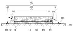
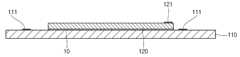
도 1은 본 발명의 일 실시예에 따른 반도체 디바이스를 도시한 단면도이다.1 is a cross-sectional view illustrating a semiconductor device according to an embodiment of the present invention.
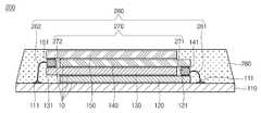
도 1을 참조하면, 본 발명의 일 실시예에 따른 반도체 디바이스(100)는 회로기판(110), 제 1 반도체 다이(120), 제 2 반도체 다이(130), 제 3 반도체 다이(140), 제 4 반도체 다이(150), 도전성 와이어(160), 솔더볼(170) 및 인캡슐란트(180)를 포함한다.1, a
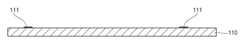
상기 회로기판(110)은 일반적인 인쇄회로기판으로, 절연층과 절연층의 상면에 형성된 다수의 배선 패턴(111)을 포함한다. 물론, 상기 회로기판(110)의 하면에도 다수의 배선 패턴이 형성될 수 있으며, 이러한 배선 패턴은 관통 비아를 통해서 회로기판(110)의 상면에 형성된 배선 패턴(111)과 전기적으로 연결된다.
The
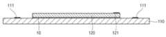
상기 제 1 반도체 다이(120)는 상기 회로기판(110)의 상면에 안착된다. 상기 제 1 반도체 다이(120)는 기본적으로 실리콘 재질로 구성되며 그 내부에 다수의 반도체 소자들이 형성된 메모리 칩일 수 있다. 이러한 제 1 반도체 다이(120)는 상기 회로기판(110)에 접착 부재(10)를 통해서 부착된다. 상기 접착 부재(10)는 통상의 액상 에폭시 접착제로 형성될 수 있으며, 상기 접착 부재(10)의 두께는 약 1~50㎛로 매우 얇게 형성된다. 또한, 상기 제 1 반도체 다이(120)의 상면에는 적어도 하나의 제 1 본드 패드(121)가 형성되며, 상기 제 1 본드 패드(121)는 상기 제 1 반도체 다이(120)의 일측에 형성된다.
The
상기 제 2 반도체 다이(130)는 상기 제 1 반도체 다이(120)의 상면에 안착된다. 상기 제 2 반도체 다이(130)는 상기 제 1 반도체 다이(120)와 동일한 형태의 반도체 다이일 수 있다. 또한, 상기 제 2 반도체 다이(130)는 상기 제 1 본드 패드(121)를 노출시키도록 상기 제 1 반도체 다이(120)의 상면에 안착되며, 접착 부재(10)를 통해서 상기 제 1 반도체 다이(120)에 부착된다. 즉, 상기 제 2 반도체 다이(130)는 상기 제 1 반도체 다이(120)의 일측에 형성된 제 1 본드 패드(121)를 외부로 노출시키도록 상기 제 1 반도체 다이(120)의 타측으로 돌출되어 상기 제 1 반도체 다이(120)에 적층된다. 다시 말해, 상기 제 2 반도체 다이(130)는 상기 제 1 반도체 다이(120)와 대응되는 위치에서 수평방향으로 일정거리 이동하여 상기 제 1 반도체 다이(120)에 적층된 것으로 볼 수 있다. 또한, 상기 제 2 반도체 다이(130)의 상면에는 적어도 하나의 제 2 본드 패드(131)가 형성되며, 상기 제 2 본드 패드(131)는 상기 제 2 반도체 다이(130)의 타측에 형성된다. 즉, 상기 제 2 본드 패드(131)와 상기 제 1 본드 패드(121)는 서로 반대측에 위치한다.
The second semiconductor die 130 is seated on the upper surface of the first semiconductor die 120. The second semiconductor die 130 may be a semiconductor die of the same type as the first semiconductor die 120. The
상기 제 3 반도체 다이(140)는 상기 제 2 반도체 다이(130)의 상면에 안착된다. 상기 제 3 반도체 다이(140)는 상기 제 1 반도체 다이(120) 및 상기 제 2 반도체 다이(130)와 동일한 형태의 반도체 다이일 수 있다. 또한, 상기 제 3 반도체 다이(140)는 상기 제 2 본드 패드(131)를 노출시키도록 상기 제 2 반도체 다이(130)의 상면에 안착되며, 접착 부재(10)를 통해서 상기 제 2 반도체 다이(130)에 부착된다. 또한, 상기 제 3 반도체 다이(140)는 상기 제 1 반도체 다이(120)의 위치와 대응되도록 상기 제 2 반도체 다이(130)에 적층된다. 따라서, 상기 제 3 반도체 다이(140)는 상기 제 2 반도체 다이(130)에 의해 외부로 노출된 상기 제 1 본드 패드(121)의 상부를 덮도록 상기 제 2 반도체 다이(130)에 안착된다. 또한, 상기 제 3 반도체 다이(140)의 하면에는 적어도 하나의 제 3 본드 패드(141)가 형성된다. 상기 제 3 본드 패드(141)는 상기 제 1 본드 패드(121)와 대응되는 위치에 형성된다. 따라서, 상기 제 3 본드 패드(141)와 상기 제 1 본드 패드(121)는 서로 마주보게 위치한다.
The third semiconductor die 140 is seated on the upper surface of the second semiconductor die 130. The third semiconductor die 140 may be a semiconductor die of the same type as the first semiconductor die 120 and the second semiconductor die 130. The
상기 제 4 반도체 다이(150)는 상기 제 3 반도체 다이(140)의 상면에 안착된다. 상기 제 4 반도체 다이(150)는 상기 제 1 반도체 다이(120), 제 2 반도체 다이(130) 및 제 3 반도체 다이(140)와 동일한 형태의 반도체 다이일 수 있다. 또한, 상기 제 4 반도체 다이(150)는 상기 제 3 반도체 다이(140)에 의해 외부로 노출된 상기 제 2 본드 패드(131)의 상부를 덮도록 상기 제 3 반도체 다이(140)의 상면에 안착되며, 접착 부재(10)를 통해서 상기 제 3 반도체 다이(140)에 부착된다. 즉, 상기 제 4 반도체 다이(150)는 상기 제 2 반도체 다이(130)의 위치와 대응되도록 상기 제 3 반도체 다이(140)에 적층된다. 따라서, 상기 제 4 반도체 다이(150)는 상기 제 1 반도체 다이(120)의 타측으로 돌출된다. 다시 말해, 상기 제 4 반도체 다이(150)는 상기 제 3 반도체 다이(140)와 대응되는 위치에서 수평방향으로 일정거리 이동하여 상기 제 3 반도체 다이(130)에 적층된 것으로 볼 수 있다. 또한, 상기 제 4 반도체 다이(150)의 하면에는 적어도 하나의 제 4 본드 패드(151)가 형성된다. 상기 제 4 본드 패드(151)는 상기 제 2 본드 패드(131)와 대응되는 위치에 형성된다. 따라서, 상기 제 4 본드 패드(151)와 상기 제 2 본드 패드(131)는 서로 마주보게 위치한다.The fourth semiconductor die 150 is seated on the upper surface of the third semiconductor die 140. The fourth semiconductor die 150 may be a semiconductor die of the same type as the first semiconductor die 120, the second semiconductor die 130, and the third semiconductor die 140. The fourth semiconductor die 150 is mounted on the upper surface of the third semiconductor die 140 so as to cover the upper portion of the
상기와 같이, 상기 제 1 반도체 다이(120)와 제 3 반도체 다이(140)는 동일한 위치에 위치하고, 상기 제 2 반도체 다이(130)와 제 4 반도체 다이(150)는 상기 제 1 반도체 다이(120)와 제 3 반도체 다이(140)로부터 수평방향으로 일정거리 이동되어 위치한다. 따라서, 상기 제 1 반도체 다이(120) 내지 제 4 반도체 다이(150)가 적층된 단면은 지그재그 형태로 서로 엇갈리게 적층되어 있다.
As described above, the first semiconductor die 120 and the third semiconductor die 140 are located at the same position, and the second semiconductor die 130 and the fourth semiconductor die 150 are located at the same positions as the first semiconductor die 120 And the third semiconductor die 140 by a predetermined distance in the horizontal direction. Therefore, the cross sections of the first semiconductor die 120 to the fourth semiconductor die 150 are stacked in a staggered manner.
상기 도전성 와이어(160)는 상기 회로기판(110)과 상기 제 1 반도체 다이(120) 및 제 2 반도체 다이(130)를 전기적으로 연결한다. 상기 도전성 와이어(160)는 제 1 도전성 와이어(161) 및 제 2 도전성 와이어(152)를 포함한다.The
상기 제 1 도전성 와이어(161)는 상기 제 1 반도체 다이(120)와 상기 회로기판(110)에 본딩되어, 상기 제 1 반도체 다이(120)와 상기 회로기판(110)을 전기적으로 연결한다. 구체적으로, 상기 제 1 도전성 와이어(161)의 일측은 상기 제 1 반도체 다이(120)의 제 1 본드 패드(121)에 본딩되고, 상기 제 1 도전성 와이어(161)의 타측은 상기 회로기판(110)의 배선 패턴(111)에 본딩된다. 또한, 상기 제 1 도전성 와이어(161)는 상기 제 2 반도체 다이(130)에 의해 외부로 노출된 상기 제 1 반도체 다이(120)의 일측에 본딩된다. 여기서, 상기 제 1,3 반도체 다이(120,140)는 동일한 위치에 위치하고 상기 제 2 반도체 다이(130)는 상기 제 1 반도체 다이(120)의 타측으로 돌출되어 적층되므로, 상기 제 1 반도체 다이(120)와 상기 제 3 반도체 다이(140) 사이에는 상기 제 2 반도체 다이(130)가 제 1 반도체 다이(120)의 타측으로 돌출된 만큼 공간이 형성된다. 따라서, 상기 제 1 도전성 와이어(161)를 상기 제 1 반도체 다이(120)에 본딩할 수 있다.The first
일반적으로, 다수의 반도체 다이를 적층하려면, 각각의 반도체 다이 사이에는 와이어 본딩을 위해 최소한의 높이인 약 50㎛이상 이격되도록 적층해야 한다. 그러나, 본 발명의 일 실시예에 따른 반도체 디바이스(100)는 제 1 내지 제 4 반도체 다이(120,130,140,150)를 서로 엇갈리게 적층함으로써, 제 1 내지 제 4 반도체 다이(120,130,140,150) 사이를 이격시키지 않더라도 와이어 본딩을 위한 공간을 확보할 수 있다. 따라서, 본 발명의 일 실시예에 따른 반도체 디바이스(100)는 다수의 반도체 다이를 적층하더라도 그 두께를 줄일 수 있으므로, 패키지의 소형화가 가능하다.In general, in order to stack a plurality of semiconductor dies, a lamination must be made between each semiconductor die such that the distance between the semiconductor dies is at least 50 mu m, which is the minimum height for wire bonding. However, the
상기 제 2 도전성 와이어(162)는 상기 제 2 반도체 다이(130)와 상기 회로기판(110)에 본딩되어, 상기 제 2 반도체 다이(130)와 상기 회로기판(110)을 전기적으로 연결한다. 구체적으로, 상기 제 2 도전성 와이어(162)의 일측은 상기 제 2 반도체 다이(130)의 제 2 본드 패드(131)에 본딩되고, 상기 제 2 도전성 와이어(162)의 타측은 상기 회로기판(110)의 배선 패턴(111)에 본딩된다. 또한, 상기 제 2 도전성 와이어(162)는 상기 제 3 반도체 다이(140)에 의해 외부로 노출된 상기 제 2 반도체 다이(130)의 타측에 본딩된다. 여기서, 상기 제 2,4 반도체 다이(130,150)는 상기 제 1,3 반도체 다이(120,140)의 타측으로 돌출되어 적층되므로, 상기 제 2 반도체 다이(130)와 상기 제 4 반도체 다이(150) 사이에는 상기 제 2,4 반도체 다이(130,150)가 상기 제 1,3 반도체 다이(120,140)의 타측으로 돌출된 만큼 공간이 형성된다. 따라서, 상기 제 2 도전성 와이어(162)를 상기 제 2 반도체 다이(130)에 본딩할 수 있다.
The second
상기 솔더볼(170)은 상기 제 1 반도체 다이(120)와 상기 제 3 반도체 다이(140) 및 상기 제 2 반도체 다이(130)와 상기 제 4 반도체 다이(150)를 전기적으로 연결한다. 상기 솔더볼(170)은 제 1 솔더볼(171) 및 제 2 솔더볼(172)을 포함한다.The
상기 제 1 솔더볼(171)은 상기 제 1 반도체 다이(120)의 제 1 본드 패드(121) 및 상기 제 3 반도체 다이(140)의 제 3 본드 패드(141)에 용착되어, 상기 제 1 반도체 다이(120)와 상기 제 3 반도체 다이(140)를 전기적으로 연결한다. 또한, 상기 제 1 솔더볼(171)은 상기 제 1 도전성 와이어(161)가 본딩된 상기 제 1 반도체 다이(120)의 제 1 본드 패드(121)에 용착된다. 따라서, 상기 제 3 반도체 다이(140)는 상기 제 1 솔더볼(171) 및 상기 제 1 도전성 와이어(161)를 통해서 상기 회로기판(110)과 전기적으로 연결될 수 있다.The
상기 제 2 솔더볼(172)은 상기 제 2 반도체 다이(130)의 제 2 본드 패드(131) 및 상기 제 4 반도체 다이(150)의 제 4 본드 패드(151)에 용착되어, 상기 제 2 반도체 다이(130)와 상기 제 4 반도체 다이(150)를 전기적으로 연결한다. 또한, 상기 제 2 솔더볼(172)은 상기 제 2 도전성 와이어(162)가 본딩된 상기 제 2 반도체 다이(130)의 제 2 본드 패드(131)에 용착된다. 따라서, 상기 제 4 반도체 다이(150)는 상기 제 2 솔더볼(172) 및 상기 제 2 도전성 와이어(162)를 통해서 상기 회로기판(110)과 전기적으로 연결될 수 있다.
The
상기 인캡슐란트(180)는 상기 회로기판(110)의 상면에 형성되며, 상기 제 1 반도체 다이(120), 제 2 반도체 다이(130), 제 3 반도체 다이(140) 및 제 4 반도체 다이(150)를 인캡슐레이션한다. 또한, 상기 인캡슐란트(180)는 상기 도전성 와이어(160) 및 상기 솔더볼(170)도 함께 인캡슐레이션한다. 상기 인캡슐란트(180)는 에폭시 계열의 수지로 형성될 수 있다. 상기 인캡슐란트(180)는 상기 회로기판(110)의 최상부에 위치하는 제 4 반도체 다이(150)의 상면을 덮도록 형성된다. 또한, 상기 인캡슐란트(180)는 상기 제 4 반도체 다이(150)의 상면을 외부로 노출시키도록 형성될 수도 있다.
The
이와 같이, 본 발명의 일 실시예에 따른 반도체 디바이스(100)는 제 1 내지 제 4 반도체 다이(120,130,140,150)를 서로 엇갈리게 적층함으로써, 도전성 와이어의 본딩을 위한 공간을 확보하여 패키지의 두께를 줄일 수 있게 된다.
As described above, the
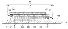
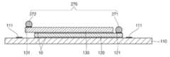
도 2는 본 발명의 다른 실시예에 따른 반도체 디바이스를 도시한 단면도이다.2 is a cross-sectional view illustrating a semiconductor device according to another embodiment of the present invention.
도 2에 도시된 반도체 디바이스(200)는 도 1에 도시된 반도체 디바이스(100)와 거의 유사하다. 따라서, 여기서는 그 차이점을 중심으로 설명하기로 한다.The
도 2를 참조하면, 본 발명의 다른 실시예에 따른 반도체 디바이스(200)는 회로기판(110), 제 1 반도체 다이(120), 제 2 반도체 다이(130), 제 3 반도체 다이(140), 제 4 반도체 다이(150), 도전성 와이어(260), 솔더볼(270) 및 인캡슐란트(280)를 포함한다.Referring to FIG. 2, a
상기 솔더볼(270)은 상기 제 1 반도체 다이(120)와 상기 제 3 반도체 다이(140) 및 상기 제 2 반도체 다이(130)와 상기 제 4 반도체 다이(150)를 전기적으로 연결한다. 상기 솔더볼(270)은 제 1 솔더볼(271) 및 제 2 솔더볼(272)을 포함한다.The
상기 제 1 솔더볼(271)은 상기 제 1 반도체 다이(120)의 제 1 본드 패드(121) 및 상기 제 3 반도체 다이(140)의 제 3 본드 패드(141)에 용착되어, 상기 제 1 반도체 다이(120)와 상기 제 3 반도체 다이(140)를 전기적으로 연결한다. 여기서, 상기 제 1,3 반도체 다이(120,140)는 동일한 위치에 위치하고 상기 제 2 반도체 다이(130)는 상기 제 1 반도체 다이(120)의 타측으로 돌출되어 적층되므로, 상기 제 1 반도체 다이(120)와 상기 제 3 반도체 다이(140) 사이에는 상기 제 2 반도체 다이(130)가 제 1 반도체 다이(120)의 타측으로 돌출된 만큼 공간이 형성된다. 따라서, 상기 제 1 솔더볼(271)은 상기 제 1 본드 패드(121) 및 제 3 본드 패드(141)에 용착될 수 있다.The
상기 제 2 솔더볼(272)은 상기 제 2 반도체 다이(130)의 제 2 본드 패드(131) 및 상기 제 4 반도체 다이(150)의 제 4 본드 패드(151)에 용착되어, 상기 제 2 반도체 다이(130)와 상기 제 4 반도체 다이(150)를 전기적으로 연결한다. 여기서, 상기 제 2,4 반도체 다이(130,150)는 상기 제 1,3 반도체 다이(120,140)의 타측으로 돌출되어 적층되므로, 상기 제 2 반도체 다이(130)와 상기 제 4 반도체 다이(150) 사이에는 상기 제 2,4 반도체 다이(130,150)가 상기 제 1,3 반도체 다이(120,140)의 타측으로 돌출된 만큼 공간이 형성된다. 따라서, 상기 제 2 솔더볼(272)은 상기 제 2 본드 패드(131) 및 제 4 본드 패드(151)에 용착될 수 있다.
The
상기 도전성 와이어(260)는 상기 회로기판(110)과 상기 제 1 반도체 다이(120), 제 2 반도체 다이(130), 제 3 반도체 다이(140) 및 제 4 반도체 다이(150)를 전기적으로 연결한다. 상기 도전성 와이어(260)는 제 1 도전성 와이어(261) 및 제 2 도전성 와이어(262)를 포함한다.The
상기 제 1 도전성 와이어(261)는 상기 제 1,3 반도체 다이(120,140)와 상기 회로기판(110)을 전기적으로 연결한다. 구체적으로, 상기 제 1 도전성 와이어(261)의 일측은 상기 제 1 솔더볼(271)에 본딩되고, 상기 제 1 도전성 와이어(261)의 타측은 상기 회로기판(110)의 배선 패턴(111)에 본딩된다. 여기서, 상기 제 1 솔더볼(271)은 상기 제 1 반도체 다이(120)와 제 3 반도체 다이(140)를 전기적으로 연결하므로, 상기 제 1 도전성 와이어(261)는 제 1,3 반도체 다이(120,140)와 회로기판(110)을 전기적으로 연결한다.The first
상기 제 2 도전성 와이어(262)는 상기 제 2,4 반도체 다이(130,150)와 상기 회로기판(110)을 전기적으로 연결한다. 구체적으로, 상기 제 2 도전성 와이어(262)의 일측은 상기 제 2 솔더볼(272)에 본딩되고, 상기 제 2 도전성 와이어(262)의 타측은 상기 회로기판(110)의 배선 패턴(111)에 본딩된다. 여기서, 상기 제 2 솔더볼(272)은 상기 제 2 반도체 다이(130)와 제 4 반도체 다이(150)를 전기적으로 연결하므로, 상기 제 2 도전성 와이어(262)는 제 2,4 반도체 다이(130,150)와 회로기판(110)을 전기적으로 연결한다.
The second
상기 인캡슐란트(280)는 상기 회로기판(110)의 상면에 형성되며, 상기 제 1 반도체 다이(120), 제 2 반도체 다이(130), 제 3 반도체 다이(140) 및 제 4 반도체 다이(150)를 인캡슐레이션한다. 또한, 상기 인캡슐란트(280)는 상기 도전성 와이어(260) 및 상기 솔더볼(270)도 함께 인캡슐레이션한다. 상기 인캡슐란트(280)는 에폭시 계열의 수지로 형성될 수 있다.
The
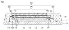
도 3은 본 발명의 또다른 실시예에 따른 반도체 디바이스를 도시한 단면도이다.3 is a cross-sectional view illustrating a semiconductor device according to another embodiment of the present invention.
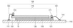
도 3에 도시된 반도체 디바이스(300)는 도 1에 도시된 반도체 디바이스(100)와 거의 유사하다. 따라서, 여기서는 그 차이점을 중심으로 설명하기로 한다.The
도 3을 참조하면, 본 발명의 또다른 실시예에 따른 반도체 디바이스(300)는 회로기판(110), 제 1 반도체 다이(120), 제 2 반도체 다이(130), 제 3 반도체 다이(140), 도전성 와이어(360), 솔더볼(370) 및 인캡슐란트(380)를 포함한다. 즉, 본 발명의 또다른 실시예에 따른 반도체 디바이스(300)는 상기 도 1에 도시된 반도체 디바이스(100)에서 제 4 반도체 다이(150)가 적층되지 않은 상태를 나타낸다.3, a
상기 도전성 와이어(360)는 상기 회로기판(110)과 상기 제 1 반도체 다이(120) 및 상기 제 3 반도체 다이(140)를 전기적으로 연결한다. 상기 도전성 와이어(360)는 제 1 도전성 와이어(361) 및 제 2 도전성 와이어(362)를 포함한다.The
상기 제 1 도전성 와이어(361)는 상기 제 1 반도체 다이(120)와 상기 회로기판(110)에 본딩되어, 상기 제 1 반도체 다이(120)와 상기 회로기판(110)을 전기적으로 연결한다. 구체적으로, 상기 제 1 도전성 와이어(361)의 일측은 상기 제 1 반도체 다이(120)의 제 1 본드 패드(121)에 본딩되고, 상기 제 1 도전성 와이어(261)의 타측은 상기 회로기판(110)의 배선 패턴(111)에 본딩된다.The first
상기 제 2 도전성 와이어(362)는 상기 제 2 반도체 다이(130)와 상기 회로기판(110)에 본딩되어, 상기 제 2 반도체 다이(130)와 상기 회로기판(110)을 전기적으로 연결한다. 구체적으로, 상기 제 2 도전성 와이어(362)의 일측은 상기 제 2 반도체 다이(130)의 제 2 본드 패드(131)에 본딩되고, 상기 제 2 도전성 와이어(362)의 타측은 상기 회로기판(110)의 배선 패턴(111)에 본딩된다.
The second
상기 솔더볼(370)은 상기 제 1 반도체 다이(120)와 상기 제 3 반도체 다이(140)를 전기적으로 연결한다. 상기 솔더볼(370)은 상기 제 1 반도체 다이(120)의 제 1 본드 패드(121) 및 상기 제 3 반도체 다이(140)의 제 3 본드 패드(141)에 용착되어, 상기 제 1 반도체 다이(120)와 상기 제 3 반도체 다이(140)를 전기적으로 연결한다. 또한, 상기 솔더볼(370)은 상기 제 1 도전성 와이어(361)가 본딩된 상기 제 1 반도체 다이(120)의 제 1 본드 패드(121)에 용착된다. 따라서, 상기 제 3 반도체 다이(140)는 상기 솔더볼(370) 및 상기 제 1 도전성 와이어(361)를 통해서 상기 회로기판(110)과 전기적으로 연결될 수 있다.
The
상기 인캡슐란트(380)는 상기 회로기판(110)의 상면에 형성되며, 상기 제 1 반도체 다이(120), 제 2 반도체 다이(130) 및 제 3 반도체 다이(140)를 인캡슐레이션한다. 또한, 상기 인캡슐란트(380)는 상기 도전성 와이어(360) 및 상기 솔더볼(370)도 함께 인캡슐레이션한다. 상기 인캡슐란트(380)는 에폭시 계열의 수지로 형성될 수 있다. 상기 인캡슐란트(380)는 상기 회로기판(110)의 최상부에 위치하는 제 3 반도체 다이(140)의 상면을 덮도록 형성된다. 또한, 상기 인캡슐란트(380)는 상기 제 3 반도체 다이(140)의 상면을 외부로 노출시키도록 형성될 수도 있다.
The
도 4는 본 발명의 또다른 실시예에 따른 반도체 디바이스를 도시한 단면도이다.4 is a cross-sectional view illustrating a semiconductor device according to another embodiment of the present invention.
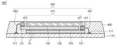
도 4에 도시된 반도체 디바이스(400)는 도 2에 도시된 반도체 디바이스(200)와 거의 유사하다. 따라서, 여기서는 그 차이점을 중심으로 설명하기로 한다.The
도 4를 참조하면, 본 발명의 또다른 실시예에 따른 반도체 디바이스(400)는 회로기판(110), 제 1 반도체 다이(120), 제 2 반도체 다이(130), 제 3 반도체 다이(140), 도전성 와이어(460), 솔더볼(470) 및 인캡슐란트(480)를 포함한다. 즉, 본 발명의 또다른 실시예에 따른 반도체 디바이스(400)는 상기 도 2에 도시된 반도체 디바이스(200)에서 제 4 반도체 디바이스(150)가 적층되지 않은 상태를 나타낸다.4, a
상기 솔더볼(470)은 상기 제 1 반도체 다이(120)와 상기 제 3 반도체 다이(140)를 전기적으로 연결한다. 상기 솔더볼(470)은 제 1 솔더볼(471) 및 제 2 솔더볼(472)을 포함한다.The
상기 제 1 솔더볼(471)은 상기 제 1 반도체 다이(120)의 제 1 본드 패드(121) 및 상기 제 3 반도체 다이(140)의 제 3 본드 패드(141)에 용착되어, 상기 제 1 반도체 다이(120)와 상기 제 3 반도체 다이(140)를 전기적으로 연결한다. 상기 제 2 솔더볼(472)은 상기 제 2 반도체 다이(130)의 제 2 본드 패드(131)에 용착된다.
The
상기 도전성 와이어(460)는 상기 회로기판(110)과 상기 제 1 반도체 다이(120), 제 2 반도체 다이(130) 및 제 3 반도체 다이(140)를 전기적으로 연결한다. 상기 도전성 와이어(460)는 제 1 도전성 와이어(461) 및 제 2 도전성 와이어(462)를 포함한다.The
상기 제 1 도전성 와이어(461)는 상기 제 1,3 반도체 다이(120,140)와 상기 회로기판(110)을 전기적으로 연결한다. 구체적으로, 상기 제 1 도전성 와이어(461)의 일측은 상기 제 1 솔더볼(471)에 본딩되고, 상기 제 1 도전성 와이어(461)의 타측은 상기 회로기판(110)의 배선 패턴(111)에 본딩된다. 여기서, 상기 제 1 솔더볼(471)은 상기 제 1 반도체 다이(120)와 제 3 반도체 다이(140)를 전기적으로 연결하므로, 상기 제 1 도전성 와이어(461)는 제 1,3 반도체 다이(120,140)와 회로기판(110)을 전기적으로 연결한다.The first
상기 제 2 도전성 와이어(462)는 상기 제 2 반도체 다이(130)와 상기 회로기판(110)을 전기적으로 연결한다. 구체적으로, 상기 제 2 도전성 와이어(462)의 일측은 상기 제 2 솔더볼(472)에 본딩되고, 상기 제 2 도전성 와이어(462)의 타측은 상기 회로기판(110)의 배선 패턴(111)에 본딩된다. 또한, 상기 제 2 도전성 와이어(462)는 상기 제 2 솔더볼(472) 없이 상기 제 2 반도체 다이(130)의 제 2 배선 패턴(131)에 직접적으로 본딩될 수 있다.
The second
상기 인캡슐란트(480)는 상기 회로기판(110)의 상면에 형성되며, 상기 제 1 반도체 다이(120), 제 2 반도체 다이(130) 및 제 3 반도체 다이(140)를 인캡슐레이션한다. 또한, 상기 인캡슐란트(480)는 상기 도전성 와이어(460) 및 상기 솔더볼(470)도 함께 인캡슐레이션한다. 상기 인캡슐란트(480)는 에폭시 계열의 수지로 형성될 수 있다.
The
다음은 본 발명의 일 실시예에 따른 반도체 디바이스의 제조 방법을 설명하기로 한다.Hereinafter, a method of manufacturing a semiconductor device according to an embodiment of the present invention will be described.
도 5는 본 발명의 일 실시예에 따른 반도체 디바이스의 제조 방법을 도시한 순서도이다. 도 6a 내지 도 6h는 본 발명의 일 실시예에 따른 반도체 디바이스의 제조 방법을 설명하기 위한 단면도이다.5 is a flowchart illustrating a method of manufacturing a semiconductor device according to an embodiment of the present invention. 6A to 6H are cross-sectional views illustrating a method of manufacturing a semiconductor device according to an embodiment of the present invention.
도 5을 참조하면, 본 발명의 일 실시예에 따른 반도체 디바이스의 제조 방법은 회로기판 준비 단계(S1), 제 1 반도체 다이 부착 단계(S2), 제 2 반도체 다이 부착 단계(S3), 와이어 본딩 단계(S4), 솔더볼 용착 단계(S5), 제 3 반도체 다이 부착 단계(S6), 제 4 반도체 다이 부착 단계(S7) 및 인캡슐레이션 단계(S8)를 포함한다. 이하에서는 도 5의 각 단계들을 도 5a 내지 도 5h를 참조하여 설명하도록 한다.Referring to FIG. 5, a method of manufacturing a semiconductor device according to an embodiment of the present invention includes a circuit board preparing step S1, a first semiconductor die attaching step S2, a second semiconductor die attaching step S3, Step S4, solder ball deposition step S5, third semiconductor die attach step S6, fourth semiconductor die attach step S7, and encapsulation step S8. Hereinafter, the respective steps of FIG. 5 will be described with reference to FIGS. 5A to 5H.
상기 회로기판 준비 단계(S1)는 본 발명의 기본이 되는 회로기판(110)을 준비하는 단계이다.The circuit board preparation step S1 is a step of preparing the
도 6a를 참조하면, 상기 회로기판 준비 단계(S1)에서는 절연층과 상기 절연층의 상면에 형성된 다수의 배선 패턴(111)을 포함하는 회로기판(110)을 준비한다.
Referring to FIG. 6A, in the circuit board preparing step S1, a
상기 제 1 반도체 다이 부착 단계(S2)는 상기 회로기판(110)의 상면에 제 1 반도체 다이(120)를 부착하는 단계이다.The first semiconductor die attaching step S2 is a step of attaching the first semiconductor die 120 to the upper surface of the
도 6b를 참조하면, 상기 제 1 반도체 다이 부착 단계(S2)에서는 상면에 제 1 본드 패드(121)가 형성된 제 1 반도체 다이(120)를 상기 회로기판(110)의 상면에 접착 부재(10)를 사용하여 부착한다. 상기 본드 패드(121)는 제 1 반도체 다이(120)의 일측에 형성된다. 여기서, 상기 제 1 반도체 다이(120)는 기본적으로 실리콘 재질로 구성되며 그 내부에 다수의 반도체 소자들이 형성된 메모리 칩일 수 있다.
6B, in the first semiconductor die attaching step S2, the first semiconductor die 120 having the
상기 제 2 반도체 다이 부착 단계(S3)는 상기 제 1 반도체 다이(120)의 상면에 제 2 반도체 다이(130)를 부착하는 단계이다.The second semiconductor die attaching step S3 is a step of attaching the second semiconductor die 130 to the upper surface of the first semiconductor die 120. [
도 6c를 참조하면, 상기 제 2 반도체 다이 부착 단계(S3)에서는 상면에 제 2 본드 패드(131)가 형성된 제 2 반도체 다이(130)를 상기 제 1 반도체 다이(120)의 상면에 접착 부재(10)를 사용하여 부착한다. 또한, 상기 제 2 반도체 다이(130)는 상기 제 1 본드 패드(121)를 노출시키도록 상기 제 1 반도체 다이(120)에 부착된다. 즉, 상기 제 2 반도체 다이(130)는 상기 제 1 반도체 다이(120)의 일측에 형성된 제 1 본드 패드(121)를 외부로 노출시키도록 상기 제 1 반도체 다이(120)의 타측으로 돌출되어 상기 제 1 반도체 다이(120)에 적층된다.
Referring to FIG. 6C, in the step of attaching the second semiconductor die (S3), a second semiconductor die 130 having a
상기 와이어 본딩 단계(S4)는 상기 회로기판(110)의 배선 패턴(111)과 상기 제 1 반도체 다이(120)의 제 1 본드 패드(121) 및 제 2 반도체 다이(130)의 제 2 본드 패드(131)를 도전성 와이어(160)로 본딩하는 단계이다.The wire bonding step S4 may be performed by bonding the
도 6d를 참조하면, 상기 와이어 본딩 단계(S4)에서는 상기 배선 패턴(111)과 상기 제 1 본드 패드(121)를 제 1 도전성 와이어(161)로 본딩하여, 상기 제 1 반도체 다이(120)와 상기 회로기판(110)을 전기적으로 연결한다. 또한, 상기 와이어 본딩 단계(S4)에서는 상기 배선 패턴(111)과 상기 제 2 본드 패드(131)를 제 2 도전성 와이어(162)로 본딩하여, 상기 제 2 반도체 다이(130)와 상기 회로기판(110)을 전기적으로 연결한다.
6D, in the wire bonding step S4, the
상기 솔더볼 용착 단계(S5)는 상기 제 1 반도체 다이(120)의 제 1 본드 패드(121) 및 제 2 반도체 다이(130)의 제 2 본드 패드(131)에 솔더볼(170)을 용착하는 단계이다.The solder ball bonding step S5 is a step of welding the
도 6e를 참조하면, 상기 솔더볼 용착 단계(S5)에서는 상기 제 1 본드 패드(121)에 제 1 솔더볼(171)을 용착하고, 상기 제 2 본드 패드(131)에 제 2 솔더볼(172)을 용착한다. 상기 제 1 솔더볼(171)은 제 1 반도체 다이(120) 및 회로기판(110)과 전기적으로 연결되고, 상기 제 2 솔더볼(172)은 제 2 반도체 다이(130) 및 회로기판(110)과 전기적으로 연결된다.
Referring to FIG. 6E, the
상기 제 3 반도체 다이 부착 단계(S6)는 상기 제 2 반도체 다이(130)의 상면에 제 3 반도체 다이(140)를 부착하는 단계이다.The third semiconductor die attaching step S6 is a step of attaching the third semiconductor die 140 to the upper surface of the second semiconductor die 130. [
도 6f를 참조하면, 상기 제 3 반도체 다이 부착 단계(S6)에서는 하면에 제 3 본드 패드(141)가 형성된 제 3 반도체 다이(140)를 상기 제 2 반도체 다이(130)의 상면에 접착 부재(10)를 사용하여 부착한다. 또한, 상기 제 3 반도체 다이(140)는 상기 제 2 본드 패드(131)를 노출시키도록 상기 제 2 반도체 다이(130)의 상면에 부착된다. 더불어, 상기 제 3 반도체 다이(140)는 상기 제 1 반도체 다이(120)와 대응되는 위치에 안착된다. 또한, 상기 제 3 반도체 다이 부착 단계(S6)에서는 상기 제 3 반도체 다이(140)의 제 3 본드 패드(141)에 상기 제 1 솔더볼(171)을 용착시킨다. 따라서, 상기 제 3 반도체 다이(140)는 상기 제 1 반도체 다이(120) 및 회로기판(110)과 전기적으로 연결된다.
Referring to FIG. 6F, in the third semiconductor die attaching step S6, a third semiconductor die 140 having a
상기 제 4 반도체 다이 부착 단계(S7)는 상기 제 3 반도체 다이(140)의 상면에 제 4 반도체 다이(150)를 부착하는 단계이다.The fourth semiconductor die attaching step S7 is a step of attaching the fourth semiconductor die 150 to the upper surface of the third semiconductor die 140. [
도 6g를 참조하면, 상기 제 4 반도체 다이 부착 단계(S7)에서는 하면에 제 4 본드 패드(151)가 형성된 제 4 반도체 다이(150)를 상기 제 3 반도체 다이(140)의 상면에 접착 부재(10)를 사용하여 부착한다. 또한, 상기 제 4 반도체 다이(150)는 상기 제 2 반도체 다이(130)와 대응되는 위치에 안착된다. 따라서, 상기 제 4 반도체 다이(150)는 상기 제 1 반도체 다이(120)의 타측으로 돌출된다. 즉, 상기 제 4 반도체 다이(150)는 상기 제 3 반도체 다이(140)와 대응되는 위치에서 수평방향으로 일정거리 이동하여 상기 제 3 반도체 다이(130)에 부착된다. 또한, 상기 제 4 반도체 다이 부착 단계(S7)에서는 상기 제 4 반도체 다이(150)의 제 4 본드 패드(151)에 상기 제 2 솔더볼(172)을 용착시킨다. 따라서, 상기 제 4 반도체 다이(150)는 상기 제 2 반도체 다이(130) 및 회로기판(110)과 전기적으로 연결된다.
6G, in the step of attaching the fourth semiconductor die S7, a fourth semiconductor die 150 having a
상기 인캡슐레이션 단계(S8)는 상기 제 1 반도체 다이(120), 제 2 반도체 다이(130), 제 3 반도체 다이(140) 및 제 4 반도체 다이(150)를 인캡슐란트(180)로 인캡슐레이션하는 단계이다.The encapsulation step S8 may include encapsulating the first semiconductor die 120, the second semiconductor die 130, the third semiconductor die 140, and the fourth semiconductor die 150 with an
도 6h를 참조하면, 상기 인캡슐레이션 단계(S8)에서는 상기 회로기판(110)의 상부에 적층된 제 1 반도체 다이(120), 제 2 반도체 다이(130), 제 3 반도체 다이(140) 및 제 4 반도체 다이(150)를 인캡슐란트(180)로 인캡슐레이션한다. 또한, 상기 인캡슐란트(180)는 상기 제 1 반도체 다이(120) 및 제 2 반도체 다이(130)에 전기적으로 연결된 도전성 와이어(160) 및 솔더볼(170)도 함께 인캡슐레이션한다. 상기 인캡슐란트(180)는 에폭시 계열의 수지로 형성될 수 있다.6H, in the encapsulation step S8, the first semiconductor die 120, the second semiconductor die 130, the third semiconductor die 140, and the third semiconductor die 140 stacked on the
상기와 같은 방법으로 제조된 반도체 디바이스(100)는 회로기판(110), 제 1 반도체 다이(120), 제 2 반도체 다이(130), 제 3 반도체 다이(140), 제 4 반도체 다이(150), 도전성 와이어(160), 솔더볼(170) 및 인캡슐란트(180)를 포함한다.The
또한, 상기와 같은 제조 방법에서 제 4 반도체 다이(150)를 부착하지 않은 채로 회로기판(110)의 상부를 인캡슐란트(180)로 인캡슐레이션하여 반도체 디바이스를 완성할 수도 있다.
In the above manufacturing method, the upper portion of the
도 7은 본 발명의 다른 실시예에 따른 반도체 디바이스의 제조 방법을 도시한 순서도이다. 도 8a 내지 도 8h는 본 발명의 다른 실시예에 따른 반도체 디바이스의 제조 방법을 설명하기 위한 단면도이다.7 is a flowchart showing a method of manufacturing a semiconductor device according to another embodiment of the present invention. 8A to 8H are cross-sectional views illustrating a method of manufacturing a semiconductor device according to another embodiment of the present invention.
도 7을 참조하면, 본 발명의 다른 실시예에 따른 반도체 디바이스의 제조 방법은 회로기판 준비 단계(S1), 제 1 반도체 다이 부착 단계(S2), 제 2 반도체 다이 부착 단계(S3), 솔더볼 용착 단계(S14), 와이어 본딩 단계(S15), 제 3 반도체 다이 부착 단계(S6), 제 4 반도체 다이 부착 단계(S7) 및 인캡슐레이션 단계(S8)를 포함한다. 즉, 본 발명의 다른 실시예에 따른 반도체 디바이스의 제조 방법은 도 5에 도시된 반도체 디바이스의 제조 방법과 비교하여, 솔더볼 용착 단계(S14)와 와이어 본딩 단계(S15)의 순서만 다르고 나머지는 모두 동일하다. 따라서, 이하에서는 솔더볼 용착 단계(S14)와 와이어 본딩 단계(S15)에 대해서만 설명하기로 한다.Referring to FIG. 7, a method of manufacturing a semiconductor device according to another embodiment of the present invention includes a circuit board preparing step S1, a first semiconductor die attaching step S2, a second semiconductor die attaching step S3, Step S14, wire bonding step S15, third semiconductor die attach step S6, fourth semiconductor die attach step S7, and encapsulation step S8. That is, the manufacturing method of the semiconductor device according to another embodiment of the present invention is different from the manufacturing method of the semiconductor device shown in FIG. 5 only in the order of the solder ball welding step S14 and the wire bonding step S15, same. Therefore, only the solder ball bonding step S14 and the wire bonding step S15 will be described below.
상기 솔더볼 용착 단계(S14)는 상기 제 1 반도체 다이(120)의 제 1 본드 패드(121) 및 상기 제 2 반도체 다이(130)의 제 2 본드 패드(131)에 솔더볼(270)을 용착하는 단계이다.The solder ball deposition step S14 includes the steps of welding the
도 8d를 참조하면, 상기 솔더볼 용착 단계(S14)에서는 상기 제 1 본드 패드(121)에 제 1 솔더볼(271)을 용착하고, 상기 제 2 본드 패드(131)에 제 2 솔더볼(272)을 용착한다. 따라서, 상기 제 1 솔더볼(271)은 제 1 반도체 다이(120)에 전기적으로 연결되고, 상기 제 2 솔더볼(272)은 제 2 반도체 다이(130)에 전기적으로 연결된다.
Referring to FIG. 8D, the
상기 와이어 본딩 단계(S15)는 상기 솔더볼(270)과 상기 회로기판(110)의 배선 패턴(111)을 도전성 와이어(260)로 본딩하는 단계이다.The wire bonding step S15 is a step of bonding the
도 8e를 참조하면, 상기 와이어 본딩 단계(S15)에서는 상기 제 1 솔더볼(271)과 상기 배선 패턴(111)을 제 1 도전성 와이어(261)로 본딩하여, 상기 제 1 반도체 다이(120)와 상기 회로기판(110)을 전기적으로 연결한다. 또한, 상기 와이어 본딩 단계(S15)에서는 상기 제 2 솔더볼(272)과 상기 배선 패턴(111)을 제 2 도전성 와이어(262)로 본딩하여, 상기 제 2 반도체 다이(130)와 상기 회로기판(110)을 전기적으로 연결한다.Referring to FIG. 8E, in the wire bonding step S15, the
더불어, 도 8h를 참조하면, 상기 인캡슐레이션 단계(S8)에서는 상기 회로기판(110)의 상부에 적층된 제 1 반도체 다이(120), 제 2 반도체 다이(130), 제 3 반도체 다이(140) 및 제 4 반도체 다이(150)를 인캡슐란트(280)로 인캡슐레이션한다. 또한, 상기 인캡슐란트(280)는 상기 제 1 반도체 다이(120) 및 제 2 반도체 다이(130)에 전기적으로 연결된 도전성 와이어(260) 및 솔더볼(270)도 함께 인캡슐레이션한다.8H, in the encapsulation step S8, the first semiconductor die 120, the second semiconductor die 130, and the third semiconductor die 140 stacked on the
따라서, 상기와 같은 방법으로 제조된 반도체 디바이스(200)는 회로기판(110), 제 1 반도체 다이(120), 제 2 반도체 다이(130), 제 3 반도체 다이(140), 제 4 반도체 다이(150), 도전성 와이어(260), 솔더볼(270) 및 인캡슐란트(280)를 포함한다.Thus, the
또한, 상기와 같은 제조 방법에서 제 4 반도체 다이(150)를 부착하지 않은 채로 회로기판(110)의 상부를 인캡슐란트(280)로 인캡슐레이션하여 반도체 디바이스를 완성할 수도 있다.
Also, in the above-described manufacturing method, the semiconductor device may be completed by encapsulating the upper portion of the
이상에서 설명한 것은 본 발명에 의한 반도체 디바이스 및 그 제조 방법을 실시하기 위한 하나의 실시예에 불과한 것으로서, 본 발명은 상기한 실시예에 한정되지 않고, 이하의 특허청구범위에서 청구하는 바와 같이 본 발명의 요지를 벗어남이 없이 당해 발명이 속하는 분야에서 통상의 지식을 가진 자라면 누구든지 다양한 변경 실시가 가능한 범위까지 본 발명의 기술적 정신이 있다고 할 것이다.
It is to be understood that the present invention is not limited to the above-described embodiment, and that various modifications and variations of the present invention are possible in light of the above teachings, It will be understood by those of ordinary skill in the art that various changes in form and details may be made therein without departing from the spirit and scope of the present invention.
100: 반도체 디바이스110: 회로기판
120: 제 1 반도체 다이130: 제 2 반도체 다이
140: 제 3 반도체 다이150: 제 4 반도체 다이
160: 도전성 와이어170: 솔더볼
180: 인캡슐란트100: semiconductor device 110: circuit board
120: first semiconductor die 130: second semiconductor die
140: third semiconductor die 150: fourth semiconductor die
160: conductive wire 170: solder ball
180: encapsulation
Claims (23)
Translated fromKorean상기 회로기판의 상면에 접착 부재로 부착되며, 상면에 제 1 본드 패드가 형성된 제 1 반도체 다이;
상기 제 1 본드 패드를 외부로 노출시키도록 상기 제 1 반도체 다이의 상면에 접착 부재로 부착되며, 상면에 제 2 본드 패드가 형성된 제 2 반도체 다이;
상기 제 2 본드 패드를 외부로 노출시키도록 상기 제 2 반도체 다이의 상면에 접착 부재로 부착되며, 하면에 제 3 본드 패드가 형성된 제 3 반도체 다이;
상기 제 2 본드 패드의 상부를 덮도록 상기 제 3 반도체 다이의 상면에 접착 부재로 부착되며, 하면에 제 4 본드 패드가 형성된 제 4 반도체 다이;
상기 회로기판과 상기 제 1 반도체 다이 및 상기 제 2 반도체 다이를 전기적으로 연결하는 도전성 와이어; 및
상기 제 1 반도체 다이와 상기 제 3 반도체 다이 및 상기 제 2 반도체 다이와 상기 제 4 반도체 다이를 전기적으로 연결하는 솔더볼을 포함하고,
상기 도전성 와이어는
상기 배선 패턴과 상기 제 1 본드 패드에 본딩된 제 1 도전성 와이어; 및
상기 배선 패턴과 상기 제 2 본드 패드에 본딩된 제 2 도전성 와이어를 포함하며,
상기 회로기판의 상부에 형성되며, 상기 제 1 반도체 다이, 제 2 반도체 다이, 제 3 반도체 다이, 제 4 반도체 다이, 도전성 와이어 및 솔더볼을 인캡슐레이션하는 인캡슐란트를 더 포함하고,
상기 제 4 반도체 다이의 상부는 상기 인캡슐란트를 통해 외부로 노출되는 것을 특징으로 하는 반도체 디바이스.A circuit board having a plurality of wiring patterns formed on an upper surface thereof;
A first semiconductor die attached to an upper surface of the circuit board with an adhesive member and having a first bond pad formed on an upper surface thereof;
A second semiconductor die attached to an upper surface of the first semiconductor die with an adhesive member to expose the first bond pad to the outside and having a second bond pad formed on an upper surface thereof;
A third semiconductor die attached to an upper surface of the second semiconductor die with an adhesive member to expose the second bond pad to the outside and having a third bond pad formed on a lower surface thereof;
A fourth semiconductor die attached with an adhesive member on an upper surface of the third semiconductor die so as to cover an upper portion of the second bond pad and having a fourth bond pad formed on a lower surface thereof;
A conductive wire electrically connecting the circuit board to the first semiconductor die and the second semiconductor die; And
And a solder ball for electrically connecting the first semiconductor die, the third semiconductor die, and the second semiconductor die to the fourth semiconductor die,
The conductive wire
A first conductive wire bonded to the wiring pattern and the first bond pad; And
And a second conductive wire bonded to the wiring pattern and the second bond pad,
Further comprising an encapsulant formed on the circuit board and encapsulating the first semiconductor die, the second semiconductor die, the third semiconductor die, the fourth semiconductor die, the conductive wire and the solder ball,
And an upper portion of the fourth semiconductor die is exposed to the outside through the encapsulant.
상기 제 1 본드 패드는 상기 제 1 반도체 다이의 일측에 형성되고,
상기 제 2 반도체 다이는 상기 제 1 반도체 다이의 타측으로 돌출된 것을 특징으로 하는 반도체 디바이스.The method according to claim 1,
Wherein the first bond pad is formed on one side of the first semiconductor die,
Wherein the second semiconductor die protrudes to the other side of the first semiconductor die.
상기 제 3 반도체 다이는 상기 제 1 반도체 다이의 위치와 대응되게 상기 제 2 반도체 다이에 부착되고,
상기 제 4 반도체 다이는 상기 제 2 반도체 다이의 위치와 대응되게 상기 제 3 반도체 다이에 부착된 것을 특징으로 하는 반도체 디바이스.3. The method of claim 2,
The third semiconductor die being attached to the second semiconductor die in correspondence with the position of the first semiconductor die,
Wherein the fourth semiconductor die is attached to the third semiconductor die in correspondence with the position of the second semiconductor die.
상기 제 3 본드 패드는 상기 제 1 본드 패드와 대응되는 위치에 형성되며, 상기 제 3 본드 패드와 상기 제 1 본드 패드는 서로 마주보는 것을 특징으로 하는 반도체 디바이스.The method according to claim 1,
Wherein the third bond pad is formed at a position corresponding to the first bond pad, and the third bond pad and the first bond pad are opposed to each other.
상기 제 4 본드 패드는 상기 제 2 본드 패드와 대응되는 위치에 형성되며, 상기 제 4 본드 패드와 상기 제 2 본드 패드는 서로 마주보는 것을 특징으로 하는 반도체 디바이스.The method according to claim 1,
Wherein the fourth bond pad is formed at a position corresponding to the second bond pad, and the fourth bond pad and the second bond pad are opposed to each other.
상기 솔더볼은
상기 제 1 본드 패드와 상기 제 3 본드 패드에 용착된 제 1 솔더볼; 및
상기 제 2 본드 패드와 상기 제 4 본드 패드에 용착된 제 2 솔더볼을 포함하는 것을 특징으로 하는 반도체 디바이스.The method according to claim 1,
The solder ball
A first solder ball deposited on the first bond pad and the third bond pad; And
And a second solder ball welded to the second bond pad and the fourth bond pad.
상기 접착 부재의 두께는 1~50 ㎛로 형성된 것을 특징으로 하는 반도체 디바이스.The method according to claim 1,
Wherein the adhesive member has a thickness of 1 to 50 占 퐉.
상면에 제 1 본드 패드가 형성된 제 1 반도체 다이를 준비하고, 상기 제 1 반도체 다이를 상기 회로기판의 상면에 접착 부재로 부착하는 제 1 반도체 다이 부착 단계;
상면에 제 2 본드 패드가 형성된 제 2 반도체 다이를 준비하고, 상기 제 1 본드 패드를 외부로 노출시키도록 상기 제 2 반도체 다이를 상기 제 1 반도체 다이의 상면에 접착 부재로 부착하는 제 2 반도체 다이 부착 단계;
상기 회로기판과 상기 제 1 반도체 다이 및 상기 제 2 반도체 다이에 도전성 와이어를 본딩하는 와이어 본딩 단계;
상기 제 1 본드 패드 및 상기 제 2 본드 패드에 솔더볼을 용착하는 솔더볼 용착 단계;
하면에 제 3 본드 패드가 형성된 제 3 반도체 다이를 준비하고, 상기 제 2 본드 패드를 노출시키도록 상기 제 3 반도체 다이를 상기 제 2 반도체 다이의 상면에 접착 부재로 부착하는 제 3 반도체 다이 부착 단계; 및
하면에 제 4 본드 패드가 형성된 제 4 반도체 다이를 준비하고, 상기 제 2 본드 패드의 상부를 덮도록 상기 제 4 반도체 다이를 상기 제 3 반도체 다이의 상면에 접착 부재로 부착하는 제 4 반도체 다이 부착 단계를 포함하고,
상기 와이어 본딩 단계에서는 상기 배선 패턴과 상기 제 1 본드 패드에 제 1 도전성 와이어를 본딩하고, 상기 배선 패턴과 상기 제 2 본드 패드에 제 2 도전성 와이어를 본딩하고,
상기 제 4 반도체 다이 부착 단계 이후에는 상기 제 1 반도체 다이, 제 2 반도체 다이, 제 3 반도체 다이, 제 4 반도체 다이, 도전성 와이어 및 솔더볼을 인캡슐란트로 인캡슐레이션하는 인캡슐레이션 단계를 더 포함하며,
상기 제 4 반도체 다이의 상부는 상기 인캡슐란트를 통해 외부로 노출되는 것을 특징으로 하는 반도체 디바이스의 제조 방법.A circuit board preparation step of preparing a circuit board having a plurality of wiring patterns formed on an upper surface thereof;
A first semiconductor die attaching step of preparing a first semiconductor die having a first bond pad on an upper surface thereof and attaching the first semiconductor die to an upper surface of the circuit board with an adhesive member;
A second semiconductor die having an upper surface formed with a second bond pad and a second semiconductor die attached with an adhesive member to the upper surface of the first semiconductor die to expose the first bond pad to the outside, Attaching step;
A wire bonding step of bonding a conductive wire to the circuit board, the first semiconductor die, and the second semiconductor die;
A solder ball fusing step of fusing a solder ball to the first bond pad and the second bond pad;
A third semiconductor die attach step of preparing a third semiconductor die on which a third bond pad is formed and attaching the third semiconductor die to an upper surface of the second semiconductor die with an adhesive member so as to expose the second bond pad ; And
A fourth semiconductor die having a fourth bond pad on its bottom surface and a fourth semiconductor die attached to the top of the third semiconductor die with an adhesive material to cover the top of the second bond pad, ≪ / RTI >
Wherein the wire bonding step includes bonding the first conductive wire to the wiring pattern and the first bond pad, bonding the second conductive wire to the wiring pattern and the second bond pad,
The method further includes encapsulating the first semiconductor die, the second semiconductor die, the third semiconductor die, the fourth semiconductor die, the conductive wire, and the solder ball encapsulant after the fourth semiconductor die attach step, ,
And the upper portion of the fourth semiconductor die is exposed to the outside through the encapsulant.
상기 제 1 반도체 다이 부착 단계에서 상기 제 1 본드 패드는 상기 제 1 반도체 다이의 일측에 형성되고,
상기 제 2 반도체 다이 부착 단계에서는 상기 제 2 반도체 다이를 상기 제 1 반도체 다이의 타측으로 돌출되게 부착하는 것을 특징으로 하는 반도체 디바이스의 제조 방법.12. The method of claim 11,
In the first semiconductor die attach step, the first bond pad is formed on one side of the first semiconductor die,
And attaching the second semiconductor die to the other side of the first semiconductor die in the step of attaching the second semiconductor die.
상기 제 3 반도체 다이 부착 단계에서는 상기 제 3 반도체 다이를 상기 제 1 반도체 다이의 위치와 대응되도록 상기 제 2 반도체 다이에 부착하고,
상기 제 4 반도체 다이 부착 단계에서는 상기 제 4 반도체 다이를 상기 제 2 반도체 다이의 위치와 대응되도록 상기 제 3 반도체 다이에 부착하는 것을 특징으로 하는 반도체 디바이스의 제조 방법13. The method of claim 12,
Attaching the third semiconductor die to the second semiconductor die so as to correspond to the position of the first semiconductor die,
And attaching the fourth semiconductor die to the third semiconductor die so as to correspond to the position of the second semiconductor die in the step of attaching the fourth semiconductor die
상기 솔더볼 용착 단계에서는 상기 제 1 본드 패드에 제 1 솔더볼을 용착하고, 상기 제 2 본드 패드에 제 2 솔더볼을 용착하는 것을 특징으로 하는 반도체 디바이스의 제조 방법.12. The method of claim 11,
Wherein the first solder ball is fused to the first bond pad and the second solder ball is fused to the second bond pad in the solder ball fusing step.
상기 제 3 반도체 다이 부착 단계에서는 상기 제 3 본드 패드가 상기 제 1 솔더볼에 전기적으로 연결되도록 부착하는 것을 특징으로 하는 반도체 디바이스의 제조 방법.16. The method of claim 15,
And attaching the third bond pad so that the third bond pad is electrically connected to the first solder ball in the third semiconductor die attach step.
상기 제 4 반도체 다이 부착 단계에서는 상기 제 4 본드 패드가 상기 제 2 솔더볼에 전기적으로 연결되도록 부착하는 것을 특징으로 하는 반도체 디바이스의 제조 방법.16. The method of claim 15,
And attaching the fourth bond pad so that the fourth bond pad is electrically connected to the second solder ball in the fourth semiconductor die attach step.
상기 접착 부재의 두께는 1~50 ㎛로 형성된 것을 특징으로 하는 반도체 디바이스의 제조 방법.12. The method of claim 11,
Wherein the adhesive member has a thickness of 1 to 50 占 퐉.
Priority Applications (1)
| Application Number | Priority Date | Filing Date | Title |
|---|---|---|---|
| KR1020130073330AKR101538540B1 (en) | 2013-06-25 | 2013-06-25 | Semiconductor device and fabricating method thereof |
Applications Claiming Priority (1)
| Application Number | Priority Date | Filing Date | Title |
|---|---|---|---|
| KR1020130073330AKR101538540B1 (en) | 2013-06-25 | 2013-06-25 | Semiconductor device and fabricating method thereof |
Publications (2)
| Publication Number | Publication Date |
|---|---|
| KR20150000782A KR20150000782A (en) | 2015-01-05 |
| KR101538540B1true KR101538540B1 (en) | 2015-07-21 |
Family
ID=52474753
Family Applications (1)
| Application Number | Title | Priority Date | Filing Date |
|---|---|---|---|
| KR1020130073330AActiveKR101538540B1 (en) | 2013-06-25 | 2013-06-25 | Semiconductor device and fabricating method thereof |
Country Status (1)
| Country | Link |
|---|---|
| KR (1) | KR101538540B1 (en) |
Families Citing this family (3)
| Publication number | Priority date | Publication date | Assignee | Title |
|---|---|---|---|---|
| US10103038B1 (en) | 2017-08-24 | 2018-10-16 | Micron Technology, Inc. | Thrumold post package with reverse build up hybrid additive structure |
| US20190067248A1 (en)* | 2017-08-24 | 2019-02-28 | Micron Technology, Inc. | Semiconductor device having laterally offset stacked semiconductor dies |
| KR102499034B1 (en)* | 2018-02-08 | 2023-02-13 | 삼성전자주식회사 | Semiconductor package including semiconductor chips |
Citations (2)
| Publication number | Priority date | Publication date | Assignee | Title |
|---|---|---|---|---|
| KR20100054602A (en)* | 2008-11-14 | 2010-05-25 | 앰코 테크놀로지 코리아 주식회사 | Semiconductor package and manufacturing method thereof |
| KR20120085522A (en)* | 2011-01-24 | 2012-08-01 | 에스케이하이닉스 주식회사 | Semiconductor chip module and semiconductor package having the same and package module |
- 2013
- 2013-06-25KRKR1020130073330Apatent/KR101538540B1/enactiveActive
Patent Citations (2)
| Publication number | Priority date | Publication date | Assignee | Title |
|---|---|---|---|---|
| KR20100054602A (en)* | 2008-11-14 | 2010-05-25 | 앰코 테크놀로지 코리아 주식회사 | Semiconductor package and manufacturing method thereof |
| KR20120085522A (en)* | 2011-01-24 | 2012-08-01 | 에스케이하이닉스 주식회사 | Semiconductor chip module and semiconductor package having the same and package module |
Also Published As
| Publication number | Publication date |
|---|---|
| KR20150000782A (en) | 2015-01-05 |
Similar Documents
| Publication | Publication Date | Title |
|---|---|---|
| US9564411B2 (en) | Semiconductor package and method of manufacturing the same | |
| KR101653856B1 (en) | Semiconductor device and manufacturing method thereof | |
| KR101190920B1 (en) | Stacked semiconductor package and method of manufacturing thereof | |
| KR101376378B1 (en) | Semiconductor device and method of manufacturing the same, and semiconductor module using the same | |
| KR101346420B1 (en) | Stacked semiconductor package and method of manufacturing the same | |
| US7829990B1 (en) | Stackable semiconductor package including laminate interposer | |
| CN108091642A (en) | semiconductor package and semiconductor process | |
| EP3104410B1 (en) | Multi-chip module, on-board computer, sensor interface substrate, and multi-chip module manufacturing method | |
| US20080073779A1 (en) | Stacked semiconductor package and method of manufacturing the same | |
| CN111052366A (en) | Semiconductor device with protection mechanism and related system, device and method thereof | |
| CN103730444A (en) | Packaging assembly and manufacture method thereof | |
| US20130307145A1 (en) | Semiconductor package and method of fabricating the same | |
| KR101332859B1 (en) | Semiconductor package having one-layer substrate and, fan-out semiconductor package and method for manufacturing the same | |
| KR20080027586A (en) | Method of manufacturing semiconductor die module and semiconductor package and semiconductor package | |
| KR101538540B1 (en) | Semiconductor device and fabricating method thereof | |
| KR102774713B1 (en) | Semiconductor package including stacked semiconductor chips | |
| KR101185457B1 (en) | Laminated semiconductor package and method of manufacturing the same | |
| WO2014203739A1 (en) | Semiconductor device and method for manufacturing same | |
| JP2009111062A (en) | Semiconductor device and manufacturing method thereof | |
| CN113299626A (en) | Conductive assembly for multi-chip packaging and manufacturing method thereof | |
| KR101046251B1 (en) | Stacked Semiconductor Packages | |
| US20080073772A1 (en) | Stacked semiconductor package and method of manufacturing the same | |
| CN107799424A (en) | Method for packaging embedded circuit | |
| JP4602223B2 (en) | Semiconductor device and semiconductor package using the same | |
| KR101334593B1 (en) | Semiconductor package and method for fabricating of the same |
Legal Events
| Date | Code | Title | Description |
|---|---|---|---|
| A201 | Request for examination | ||
| PA0109 | Patent application | Patent event code:PA01091R01D Comment text:Patent Application Patent event date:20130625 | |
| PA0201 | Request for examination | ||
| E902 | Notification of reason for refusal | ||
| PE0902 | Notice of grounds for rejection | Comment text:Notification of reason for refusal Patent event date:20141113 Patent event code:PE09021S01D | |
| PG1501 | Laying open of application | ||
| E701 | Decision to grant or registration of patent right | ||
| PE0701 | Decision of registration | Patent event code:PE07011S01D Comment text:Decision to Grant Registration Patent event date:20150518 | |
| PR0701 | Registration of establishment | Comment text:Registration of Establishment Patent event date:20150715 Patent event code:PR07011E01D | |
| PR1002 | Payment of registration fee | Payment date:20150715 End annual number:3 Start annual number:1 | |
| PG1601 | Publication of registration | ||
| FPAY | Annual fee payment | Payment date:20180710 Year of fee payment:4 | |
| PR1001 | Payment of annual fee | Payment date:20180710 Start annual number:4 End annual number:4 | |
| FPAY | Annual fee payment | Payment date:20190711 Year of fee payment:5 | |
| PR1001 | Payment of annual fee | Payment date:20190711 Start annual number:5 End annual number:5 | |
| PR1001 | Payment of annual fee | Payment date:20200710 Start annual number:6 End annual number:6 | |
| PR1001 | Payment of annual fee | Payment date:20210713 Start annual number:7 End annual number:7 | |
| PR1001 | Payment of annual fee | Payment date:20220712 Start annual number:8 End annual number:8 | |
| PR1001 | Payment of annual fee | Payment date:20240702 Start annual number:10 End annual number:10 | |
| PR1001 | Payment of annual fee | Payment date:20250701 Start annual number:11 End annual number:11 |