KR101535227B1 - Method for forming fine pattern using block copolymer - Google Patents
Method for forming fine pattern using block copolymerDownload PDFInfo
- Publication number
- KR101535227B1 KR101535227B1KR1020080138549AKR20080138549AKR101535227B1KR 101535227 B1KR101535227 B1KR 101535227B1KR 1020080138549 AKR1020080138549 AKR 1020080138549AKR 20080138549 AKR20080138549 AKR 20080138549AKR 101535227 B1KR101535227 B1KR 101535227B1
- Authority
- KR
- South Korea
- Prior art keywords
- layer
- organic
- pattern
- forming
- photoresist pattern
- Prior art date
- Legal status (The legal status is an assumption and is not a legal conclusion. Google has not performed a legal analysis and makes no representation as to the accuracy of the status listed.)
- Active
Links
Images


Classifications
- G—PHYSICS
- G03—PHOTOGRAPHY; CINEMATOGRAPHY; ANALOGOUS TECHNIQUES USING WAVES OTHER THAN OPTICAL WAVES; ELECTROGRAPHY; HOLOGRAPHY
- G03F—PHOTOMECHANICAL PRODUCTION OF TEXTURED OR PATTERNED SURFACES, e.g. FOR PRINTING, FOR PROCESSING OF SEMICONDUCTOR DEVICES; MATERIALS THEREFOR; ORIGINALS THEREFOR; APPARATUS SPECIALLY ADAPTED THEREFOR
- G03F7/00—Photomechanical, e.g. photolithographic, production of textured or patterned surfaces, e.g. printing surfaces; Materials therefor, e.g. comprising photoresists; Apparatus specially adapted therefor
- G03F7/0002—Lithographic processes using patterning methods other than those involving the exposure to radiation, e.g. by stamping
- B—PERFORMING OPERATIONS; TRANSPORTING
- B81—MICROSTRUCTURAL TECHNOLOGY
- B81C—PROCESSES OR APPARATUS SPECIALLY ADAPTED FOR THE MANUFACTURE OR TREATMENT OF MICROSTRUCTURAL DEVICES OR SYSTEMS
- B81C1/00—Manufacture or treatment of devices or systems in or on a substrate
- B81C1/00015—Manufacture or treatment of devices or systems in or on a substrate for manufacturing microsystems
- B81C1/00023—Manufacture or treatment of devices or systems in or on a substrate for manufacturing microsystems without movable or flexible elements
- B81C1/00031—Regular or irregular arrays of nanoscale structures, e.g. etch mask layer
- B—PERFORMING OPERATIONS; TRANSPORTING
- B82—NANOTECHNOLOGY
- B82Y—SPECIFIC USES OR APPLICATIONS OF NANOSTRUCTURES; MEASUREMENT OR ANALYSIS OF NANOSTRUCTURES; MANUFACTURE OR TREATMENT OF NANOSTRUCTURES
- B82Y10/00—Nanotechnology for information processing, storage or transmission, e.g. quantum computing or single electron logic
- B—PERFORMING OPERATIONS; TRANSPORTING
- B82—NANOTECHNOLOGY
- B82Y—SPECIFIC USES OR APPLICATIONS OF NANOSTRUCTURES; MEASUREMENT OR ANALYSIS OF NANOSTRUCTURES; MANUFACTURE OR TREATMENT OF NANOSTRUCTURES
- B82Y40/00—Manufacture or treatment of nanostructures
- G—PHYSICS
- G03—PHOTOGRAPHY; CINEMATOGRAPHY; ANALOGOUS TECHNIQUES USING WAVES OTHER THAN OPTICAL WAVES; ELECTROGRAPHY; HOLOGRAPHY
- G03F—PHOTOMECHANICAL PRODUCTION OF TEXTURED OR PATTERNED SURFACES, e.g. FOR PRINTING, FOR PROCESSING OF SEMICONDUCTOR DEVICES; MATERIALS THEREFOR; ORIGINALS THEREFOR; APPARATUS SPECIALLY ADAPTED THEREFOR
- G03F7/00—Photomechanical, e.g. photolithographic, production of textured or patterned surfaces, e.g. printing surfaces; Materials therefor, e.g. comprising photoresists; Apparatus specially adapted therefor
- G03F7/26—Processing photosensitive materials; Apparatus therefor
- G03F7/40—Treatment after imagewise removal, e.g. baking
- G03F7/405—Treatment with inorganic or organometallic reagents after imagewise removal
- H—ELECTRICITY
- H01—ELECTRIC ELEMENTS
- H01L—SEMICONDUCTOR DEVICES NOT COVERED BY CLASS H10
- H01L21/00—Processes or apparatus adapted for the manufacture or treatment of semiconductor or solid state devices or of parts thereof
- H01L21/02—Manufacture or treatment of semiconductor devices or of parts thereof
- H01L21/027—Making masks on semiconductor bodies for further photolithographic processing not provided for in group H01L21/18 or H01L21/34
- H01L21/0271—Making masks on semiconductor bodies for further photolithographic processing not provided for in group H01L21/18 or H01L21/34 comprising organic layers
- H01L21/0273—Making masks on semiconductor bodies for further photolithographic processing not provided for in group H01L21/18 or H01L21/34 comprising organic layers characterised by the treatment of photoresist layers
- H01L21/0274—Photolithographic processes
- H01L21/0276—Photolithographic processes using an anti-reflective coating
- H—ELECTRICITY
- H01—ELECTRIC ELEMENTS
- H01L—SEMICONDUCTOR DEVICES NOT COVERED BY CLASS H10
- H01L21/00—Processes or apparatus adapted for the manufacture or treatment of semiconductor or solid state devices or of parts thereof
- H01L21/02—Manufacture or treatment of semiconductor devices or of parts thereof
- H01L21/027—Making masks on semiconductor bodies for further photolithographic processing not provided for in group H01L21/18 or H01L21/34
- H01L21/033—Making masks on semiconductor bodies for further photolithographic processing not provided for in group H01L21/18 or H01L21/34 comprising inorganic layers
- H01L21/0334—Making masks on semiconductor bodies for further photolithographic processing not provided for in group H01L21/18 or H01L21/34 comprising inorganic layers characterised by their size, orientation, disposition, behaviour, shape, in horizontal or vertical plane
- H01L21/0337—Making masks on semiconductor bodies for further photolithographic processing not provided for in group H01L21/18 or H01L21/34 comprising inorganic layers characterised by their size, orientation, disposition, behaviour, shape, in horizontal or vertical plane characterised by the process involved to create the mask, e.g. lift-off masks, sidewalls, or to modify the mask, e.g. pre-treatment, post-treatment
- H—ELECTRICITY
- H01—ELECTRIC ELEMENTS
- H01L—SEMICONDUCTOR DEVICES NOT COVERED BY CLASS H10
- H01L21/00—Processes or apparatus adapted for the manufacture or treatment of semiconductor or solid state devices or of parts thereof
- H01L21/02—Manufacture or treatment of semiconductor devices or of parts thereof
- H01L21/027—Making masks on semiconductor bodies for further photolithographic processing not provided for in group H01L21/18 or H01L21/34
- H01L21/033—Making masks on semiconductor bodies for further photolithographic processing not provided for in group H01L21/18 or H01L21/34 comprising inorganic layers
- H01L21/0334—Making masks on semiconductor bodies for further photolithographic processing not provided for in group H01L21/18 or H01L21/34 comprising inorganic layers characterised by their size, orientation, disposition, behaviour, shape, in horizontal or vertical plane
- H01L21/0338—Process specially adapted to improve the resolution of the mask
- H—ELECTRICITY
- H01—ELECTRIC ELEMENTS
- H01L—SEMICONDUCTOR DEVICES NOT COVERED BY CLASS H10
- H01L21/00—Processes or apparatus adapted for the manufacture or treatment of semiconductor or solid state devices or of parts thereof
- H01L21/02—Manufacture or treatment of semiconductor devices or of parts thereof
- H01L21/04—Manufacture or treatment of semiconductor devices or of parts thereof the devices having potential barriers, e.g. a PN junction, depletion layer or carrier concentration layer
- H01L21/18—Manufacture or treatment of semiconductor devices or of parts thereof the devices having potential barriers, e.g. a PN junction, depletion layer or carrier concentration layer the devices having semiconductor bodies comprising elements of Group IV of the Periodic Table or AIIIBV compounds with or without impurities, e.g. doping materials
- H01L21/30—Treatment of semiconductor bodies using processes or apparatus not provided for in groups H01L21/20 - H01L21/26
- H01L21/31—Treatment of semiconductor bodies using processes or apparatus not provided for in groups H01L21/20 - H01L21/26 to form insulating layers thereon, e.g. for masking or by using photolithographic techniques; After treatment of these layers; Selection of materials for these layers
- H01L21/3105—After-treatment
- H01L21/311—Etching the insulating layers by chemical or physical means
- H01L21/31144—Etching the insulating layers by chemical or physical means using masks
- H—ELECTRICITY
- H01—ELECTRIC ELEMENTS
- H01L—SEMICONDUCTOR DEVICES NOT COVERED BY CLASS H10
- H01L21/00—Processes or apparatus adapted for the manufacture or treatment of semiconductor or solid state devices or of parts thereof
- H01L21/02—Manufacture or treatment of semiconductor devices or of parts thereof
- H01L21/04—Manufacture or treatment of semiconductor devices or of parts thereof the devices having potential barriers, e.g. a PN junction, depletion layer or carrier concentration layer
- H01L21/18—Manufacture or treatment of semiconductor devices or of parts thereof the devices having potential barriers, e.g. a PN junction, depletion layer or carrier concentration layer the devices having semiconductor bodies comprising elements of Group IV of the Periodic Table or AIIIBV compounds with or without impurities, e.g. doping materials
- H01L21/30—Treatment of semiconductor bodies using processes or apparatus not provided for in groups H01L21/20 - H01L21/26
- H01L21/31—Treatment of semiconductor bodies using processes or apparatus not provided for in groups H01L21/20 - H01L21/26 to form insulating layers thereon, e.g. for masking or by using photolithographic techniques; After treatment of these layers; Selection of materials for these layers
- H01L21/3205—Deposition of non-insulating-, e.g. conductive- or resistive-, layers on insulating layers; After-treatment of these layers
- H01L21/321—After treatment
- H01L21/3213—Physical or chemical etching of the layers, e.g. to produce a patterned layer from a pre-deposited extensive layer
- H01L21/32139—Physical or chemical etching of the layers, e.g. to produce a patterned layer from a pre-deposited extensive layer using masks
- B—PERFORMING OPERATIONS; TRANSPORTING
- B81—MICROSTRUCTURAL TECHNOLOGY
- B81C—PROCESSES OR APPARATUS SPECIALLY ADAPTED FOR THE MANUFACTURE OR TREATMENT OF MICROSTRUCTURAL DEVICES OR SYSTEMS
- B81C2201/00—Manufacture or treatment of microstructural devices or systems
- B81C2201/01—Manufacture or treatment of microstructural devices or systems in or on a substrate
- B81C2201/0101—Shaping material; Structuring the bulk substrate or layers on the substrate; Film patterning
- B81C2201/0147—Film patterning
- B81C2201/0149—Forming nanoscale microstructures using auto-arranging or self-assembling material
Landscapes
- Engineering & Computer Science (AREA)
- Chemical & Material Sciences (AREA)
- Physics & Mathematics (AREA)
- General Physics & Mathematics (AREA)
- Manufacturing & Machinery (AREA)
- Microelectronics & Electronic Packaging (AREA)
- Condensed Matter Physics & Semiconductors (AREA)
- Nanotechnology (AREA)
- Power Engineering (AREA)
- Computer Hardware Design (AREA)
- Inorganic Chemistry (AREA)
- Crystallography & Structural Chemistry (AREA)
- Analytical Chemistry (AREA)
- Organic Chemistry (AREA)
- Theoretical Computer Science (AREA)
- Mathematical Physics (AREA)
- Exposure Of Semiconductors, Excluding Electron Or Ion Beam Exposure (AREA)
- Photosensitive Polymer And Photoresist Processing (AREA)
Abstract
Translated fromKoreanDescription
Translated fromKorean본 발명은 반도체 소자 제조를 위한 미세 패턴 형성 방법에 관한 것으로, 특히 블록 공중합체를 이용한 미세 패턴 형성 방법에 관한 것이다.The present invention relates to a method for forming a fine pattern for a semiconductor device, and more particularly, to a method for forming a fine pattern using a block copolymer.
반도체 소자의 집적도가 증가함에 따라, 평면적으로 각 단위 셀이 차지하는 면적이 감소하게 되었다. 이와 같은 단위 셀 면적의 감소에 대응하여, 수 내지 수 십 nm 수준의 보다 작은 나노 스케일의 CD (Critical Dimension)의 디자인 룰(design rule)이 적용되고, 이에 따라 나노 스케일의 개구 사이즈(opening size)를 가지는 미세 콘택홀 패턴 또는 나노 스케일의 폭을 가지는 미세 라인 패턴과 같은 미세 패턴을 형성하기 위한 새로운 기술이 요구되고 있다.As the degree of integration of semiconductor devices increases, the area occupied by each unit cell decreases in a plan view. In response to such a decrease in the unit cell area, a design rule of a smaller nanoscale CD (Critical Dimension) of a few to a few tens of nanometers is applied, and thus a nanoscale opening size, There is a need for a new technique for forming a fine pattern such as a fine contact hole pattern having a width of a nanometer scale or a fine line pattern having a nanoscale width.
반도체 소자 제조를 위한 미세 패턴 형성을 위하여 탑-다운 (top-down) 방식의 포토리소그래피 (photolithography) 기술에만 의존하는 경우 광원의 파장 및 광학 시스템의 해상 한계 등으로 인해 분해능을 향상시키는 데 제한이 있다.There is a limitation in improving the resolution due to the wavelength of the light source and the resolution limit of the optical system when relying solely on the top-down photolithography technology for the fine pattern formation for semiconductor device fabrication .
포토리소그래피 기술에서의 분해능 한계를 극복하고 차세대 미세 가공 기술을 개발하기 위한 노력중 하나로서 분자들의 자기조립 현상을 이용한 바텀-업 (bottom-up) 방식의 미세 구조 형성 방법들이 시도되었다. 그러나, 지금까지 제안된 분자들의 자기조립을 이용한 미세 패턴 형성 방법은 실험적 수준에 불과하여 실제 반도체 소자 제조를 위한 미세 패턴을 구현하는 데에는 어려움이 있다. 따라서, 고집적 반도체 소자에서 요구되는 나노 스케일의 미세 패턴을 형성하는 데 있어서 소자 제조 공정에 적용하기 쉽고 대량 생산 가능하도록 대면적의 반복 구조를 형성하는 것이 가능한 미세 패턴 형성 방법이 요구된다.As one of efforts to overcome the resolution limit in photolithography technology and develop next-generation microfabrication technology, attempts have been made to form bottom-up microstructures using self-assembly phenomena of molecules. However, the method of forming fine patterns using self-assembly of the molecules so far is only at an experimental level, so that it is difficult to realize a fine pattern for manufacturing semiconductor devices. Therefore, there is a need for a method of forming a fine pattern capable of forming a large-area repeating structure so that it can be easily applied to a device manufacturing process and can be mass-produced in forming a nano-scale fine pattern required for a highly integrated semiconductor device.
본 발명의 목적은 포토리소그래피 공정에서의 해상 한계를 초월하는 고집적 반도체 소자 제조에 필요한 미세 피치의 패턴을 비교적 용이하게 구현할 수 있는 미세 패턴 형성 방법을 제공하는 것이다.It is an object of the present invention to provide a method of forming a fine pattern which can relatively easily realize a fine pitch pattern necessary for manufacturing a highly integrated semiconductor device that exceeds the marginal limit in the photolithography process.
상기 목적을 달성하기 위하여, 본 발명에 따른 미세 패턴 형성 방법에서는 기판상에 유기 가이드층을 형성한다. 상기 유기 가이드층 위에 상기 유기 가이드층을 노출시키는 복수의 개구가 형성된 포토레지스트 패턴을 형성한다. 상기 개구를 통해 노출된 유기 가이드층의 노출 부분과 상기 포토레지스트 패턴 위에 블록 공중합체를 포함하는 물질층을 형성한다. 상기 물질층의 상분리를 통해 상기 물질층의 성분들을 재배열시켜, 상기 유기 가이드층의 노출 부분과 상기 포토레지스트 패턴 위에 서로 다른 성분의 반복 단위를 가지는 복수의 제1 블록 및 복수의 제2 블록이 각각 교대로 반복 배치되어 있는 미세 패턴층을 형성한다.In order to accomplish the above object, in the method of forming a fine pattern according to the present invention, an organic guide layer is formed on a substrate. A photoresist pattern having a plurality of openings exposing the organic guiding layer is formed on the organic guiding layer. An exposed portion of the organic guiding layer exposed through the opening and a material layer including a block copolymer on the photoresist pattern are formed. A plurality of first blocks and a plurality of second blocks each having a repetitive unit of different components on the exposed portion of the organic guiding layer and the photoresist pattern by rearranging the components of the material layer through phase separation of the material layer, Thereby forming a fine pattern layer repeatedly alternately arranged.
상기 유기 가이드층은 유기 반사방지막 또는 HMDS막 (hexamethyldisilazane film)으로 이루어질 수 있다.The organic guiding layer may be formed of an organic antireflection film or an HMDS film (hexamethyldisilazane film).
상기 미세 패턴층의 복수의 제1 블록은 각각 상기 포토레지스트 패턴에 형성된 개구의 폭과 동일한 폭을 가질 수 있다.The plurality of first blocks of the fine pattern layer may each have a width equal to the width of the opening formed in the photoresist pattern.
상기 물질층의 성분들을 재배열시키기 위하여 상기 가이드층의 노출 부분과 상기 포토레지스트 패턴의 표면 특성 차이를 이용할 수 있다.The difference in surface characteristics of the photoresist pattern and the exposed portion of the guide layer can be used to rearrange the components of the material layer.
상기 미세 패턴층에서 상기 복수의 제1 블록 및 복수의 제2 블록중 친수성이 더 큰 블록이 상기 유기 가이드층의 노출 부분 위에 자기조립될 수 있다.In the fine pattern layer, a block having a larger hydrophilicity among the plurality of first blocks and the plurality of second blocks may be self-assembled on the exposed portion of the organic guide layer.
상기 미세 패턴층을 형성하는 단계는 상기 물질층의 상분리를 통해 상기 물질층의 성분들을 재배열시키기 위하여 상기 블록 공중합체의 유리전이온도 보다 더 높은 온도하에서 상기 물질층을 어닐링하는 단계를 포함할 수 있다.The step of forming the micropatterned layer may comprise annealing the material layer at a temperature higher than the glass transition temperature of the block copolymer to rearrange the components of the material layer through phase separation of the material layer have.
본 발명에 따른 미세 패턴 형성 방법은 상기 미세 패턴층에서 복수의 제1 블록 및 복수의 제2 블록 중 어느 하나를 제거하여 상기 유기 가이드층의 노출 부분 및 상기 포토레지스트 패턴의 상면중 일부를 노출시키는 미세 패턴 마스크를 형성하는 단계와, 상기 미세 패턴 마스크를 식각 마스크로 하여 상기 유기 가이드층의 노출 부분 및 상기 포토레지스트 패턴의 상면중 일부를 식각하는 단계를 더 포함할 수 있다. 또한, 상기 기판상에 유기 가이드층을 형성하기 전에, 상기 기판상에 피식각막을 형성하는 단계를 더 포함할 수 있으며, 이 때 상기 유기 가이드층은 상기 피식각막 위에 형성된다. 그리고, 상기 유기 가이드층의 노출 부분 및 상기 포토레지스트 패턴의 상면중 일부를 식각한 후, 상기 미세 패턴 마스크를 식각 마스크로 하여 상기 피식각막을 식각하는 단계를 더 포함할 수 있다.In the method of forming a fine pattern according to the present invention, any one of a plurality of first blocks and a plurality of second blocks may be removed from the fine pattern layer to expose a part of the exposed portion of the organic guide layer and the top surface of the photoresist pattern Forming a fine pattern mask; and etching the exposed portion of the organic guiding layer and a part of the top surface of the photoresist pattern using the fine pattern mask as an etching mask. Further, the method may further include forming a corneal epithelial layer on the substrate before forming the organic guiding layer on the substrate, wherein the organic guiding layer is formed on the corneal epithelium. Etching the exposed portion of the organic guiding layer and a portion of the top surface of the photoresist pattern, and then etching the corneal epithelium using the fine pattern mask as an etching mask.
본 발명에서는 포토리소그래피 공정에서의 해상 한계를 초월하는 고집적 반도체 소자 제조에 필요한 미세 피치의 패턴을 형성하기 위하여, 먼저 기판상에 친수성 기를 가지는 폴리머 블록에 대하여 친화도가 큰 유기 가이드층을 형성한 후, 상기 유기 가이드층의 상면중 일부가 노출되도록 상기 유기 가이드층 위에 제1 피 치로 반복 형성되는 복수의 개구가 형성된 포토레지스트 패턴을 형성한다. 그 후, 상기 개구를 통해 노출되는 유기 가이드층의 노출 표면과 상기 포토레지스트 패턴의 표면과의 표면 특성 차이를 이용하여 상기 유기 가이드층의 노출 표면 및 상기 포토레지스트 패턴의 상면 위에 블록 공중합체의 자기조립 구조를 형성함으로써 상기 제1 피치 보다 작은 제2 피치로 반복 배치되는 미세 패턴들을 형성한다.In the present invention, in order to form a fine pitch pattern necessary for manufacturing a highly integrated semiconductor device that exceeds the marginal limit in the photolithography process, an organic guide layer having a high affinity to a polymer block having a hydrophilic group is first formed on a substrate , And a photoresist pattern is formed on the organic guiding layer so as to expose a part of the top surface of the organic guiding layer, the photoresist pattern having a plurality of openings repeatedly formed by the first pitch. Thereafter, on the exposed surface of the organic guiding layer and on the top surface of the photoresist pattern using the difference in surface characteristics between the exposed surface of the organic guiding layer exposed through the opening and the surface of the photoresist pattern, Thereby forming fine patterns repeatedly arranged at a second pitch smaller than the first pitch.
본 발명에 의하면, 블록 공중합체의 자기조립 현상을 통하여 얻어진 분자크기 수준의 미세 구조를 반도체 소자 제조 과정에 이용한다. 블록 공중합체의 자기조립 현상을 이용하여 패턴의 밀도를 증가시키므로 미세 패턴의 밀도 증가를 위한 별도의 가공 공정을 추가할 필요 없이 패턴의 밀도를 용이하게 증가시킬 수 있다.According to the present invention, a microstructure having a molecular size level obtained through self-assembly of a block copolymer is used in a semiconductor device manufacturing process. Since the density of the pattern is increased by using the self-assembly phenomenon of the block copolymer, the density of the pattern can be easily increased without adding a separate processing step for increasing the density of the fine pattern.
또한, 본 발명에 따른 미세 패턴 형성 방법에서는 포토리소그래피 공정에 의해 원하는 피치보다 큰 피치로 반복 배치되는 예비 패턴을 형성한 후, 상기 예비 패턴에서의 표면 특성 차이를 이용하여 블록 공중합체의 자기조립 구조의 배향을 임의의 방향 및 임의의 형태로 유도할 수 있으므로 다양한 형태의 미세 패턴을 형성할 수 있다. 그리고, 상기 예비 패턴에서 설정된 피치에 따라 자발적인 자기조립 과정을 통해 패턴 밀도가 증가되는 배율을 조절할 수 있으므로 통상의 포토리소그래피 공정에서 구현하기 어려운 미세 피치의 반복 구조로 형성되는 미세 패턴을 용이하게 제조할 수 있다.In the method for forming a fine pattern according to the present invention, after a preliminary pattern repeatedly arranged at a pitch larger than a desired pitch is formed by a photolithography process, the self-assembly structure of the block copolymer Can be induced in an arbitrary direction and in an arbitrary shape, so that various types of fine patterns can be formed. Since the magnification of the pattern density can be adjusted by spontaneous self-assembly process according to the pitch set in the preliminary pattern, it is possible to easily manufacture a fine pattern formed with a fine pitch repeating structure which is difficult to realize in a normal photolithography process .
본 발명에 따른 미세 패턴 형성 방법은 통상의 포토리소그래피 공정에서와는 달리 블록 공중합체의 자발적인 자기조립 특성을 이용하여 분자 크기 수준까지의 미세 구조를 형성할 수 있으며, 따라서 별도의 설비를 이용하지 않고도 대면적의 미세 패턴 반복 구조를 저단가로 용이하게 형성할 수 있다.The method of forming a fine pattern according to the present invention can form a microstructure up to a molecular size level by utilizing the spontaneous self-assembling property of the block copolymer, unlike in a conventional photolithography process. Therefore, It is possible to easily form the fine pattern repeating structure of FIG.
본 발명에서는 포토리소그래피 공정에서의 해상 한계를 초월하는 고집적 반도체 소자 제조에 필요한 미세 피치의 패턴을 구현하기 위하여 폴리머의 자기조립 특성을 이용하여 패턴의 피치를 조절함으로써 패턴 밀도를 증가시킨다. 블록 공중합체의 상분리 현상을 이용하면 자발적 자기조립을 통하여 반복적으로 배치되는 미세 구조들을 얻을 수 있다. 블록 공중합체의 자기조립 특성을 이용한 패턴 형성 공정은 포토리소그래피 공정과는 달리 얻어지는 미세 패턴의 크기가 단일 분자층 두께와 거의 비슷하게 되어 기존의 포토리소그래피 공정에서의 분해능 한계를 초월하는 미세 패턴을 형성할 수 있다.In the present invention, the pattern density is increased by adjusting the pitch of the pattern using the self-assembling property of the polymer in order to realize a fine pitch pattern required for manufacturing a highly integrated semiconductor device that exceeds the marginal limit in the photolithography process. By using the phase separation phenomenon of the block copolymer, it is possible to obtain microstructures repeatedly arranged through spontaneous self-assembly. Unlike the photolithography process, the pattern formation process using the self-assembling property of the block copolymer causes the size of the fine pattern to be obtained to be approximately equal to the thickness of the single molecule layer, thereby forming a fine pattern exceeding the resolution limit in the conventional photolithography process .
블록 공중합체는 두 가지 이상의 서로 다른 구조를 가지는 고분자 블록들이 공유 결합을 통해 하나의 고분자로 결합된 형태의 기능성 고분자이다. 블록 공중합체를 구성하는 각 고분자 블록들은 각각의 화학 구조의 차이로 인해 서로 다른 섞임 특성 및 선택적 용해도를 가진다. 이는 블록 공중합체가 용액상 혹은 고체상에서 상분리 또는 선택적 용해에 의해 자기조립 구조 (self-assembled structure)를 형성하게 되는 원인이 된다. 블록 공중합체가 자기조립을 통해 특정 형상의 미세 구조를 형성하는 것은 상기 블록 고분자의 물리/화학적 특성에 영향을 받는다. 예를 들면, 2 개의 서로 다른 고분자로 이루어진 블록 공중합체 (diblock copolymer)가 벌크(bulk) 기판상에서 자기조립되는 경우, 블록 공중합체를 구성하는 각 고분자 블록들의 부피 비율 (volume fraction)은 각 고분자 블록의 분자량에 의해 일차 적으로 영향을 받는다. 블록 공중합체의 자기조립 구조는 블록 공중합체를 구성하는 각 고분자 블록들의 부피 비율, 온도, 분자의 크기 등에 따라 3차원 구조인 큐빅(cubic) 및 이중 나선형 (double gyroid), 그리고 2차원 구조인 조밀 육방 기둥 (hexagonal packed column) 구조 및 판상 (lamellar) 구조 등과 같은 다양한 구조들 중 어느 하나의 구조가 결정된다. 이 때, 각 구조 내에서의 각 고분자 블록의 크기는 해당 고분자 블록의 분자량에 비례하게 된다.A block copolymer is a functional polymer in which two or more polymer blocks having different structures are bonded to each other through a covalent bond as a single polymer. Each of the polymer blocks constituting the block copolymer has different mixing characteristics and selective solubility due to the difference in chemical structure. This causes the block copolymer to form a self-assembled structure by phase separation or selective dissolution in solution or solid phase. The fact that the block copolymer forms a microstructure of a specific shape through self-assembly is affected by the physical / chemical properties of the block polymer. For example, when a diblock copolymer consisting of two different polymers is self-assembled on a bulk substrate, the volume fraction of each polymer block constituting the block copolymer is determined by the ratio of the volume fraction of each polymer block Lt; RTI ID = 0.0 > molecular weight. ≪ / RTI > The self-assembling structure of the block copolymer is a three-dimensional cubic structure, a double gyroid structure, and a two-dimensional structure, depending on the volume ratio, temperature, and molecular size of each polymer block constituting the block copolymer. A structure of any one of various structures such as a hexagonal packed column structure and a lamellar structure is determined. In this case, the size of each polymer block in each structure is proportional to the molecular weight of the corresponding polymer block.
반도체 소자의 미세 패턴을 형성하는 데 있어서 2차원 구조인 육방 기둥 (hexagonal column) 구조 또는 층상 (lamellar) 구조로 자기조립되는 블록 공중합체들을 이용할 수 있다. 육방 기둥 구조를 이용하는 경우, 원통형의 기둥들이 육각형으로 채워져서 형성되는 구조이므로 얻어지는 구조의 배향이 비교적 단순하며, 기둥의 배향 방향에 따라 라인 앤드 스페이스 (line and space) 패턴을 형성하거나, 반복적으로 배열되는 복수의 홀(hole) 패턴 구조를 형성할 수 있다. 판상 구조는 2 차원 판형 구조가 반복적으로 중첩되어 있는 것으로서, 상기 판상 구조의 블록 공중합체가 기판 표면에 수직으로 배향되는 경우, 아스펙트비(aspect ratio)가 큰 라인 앤드 스페이스 패턴을 형성할 수 있다.In forming a fine pattern of a semiconductor device, block copolymers self-assembled into a hexagonal column structure or a lamellar structure having a two-dimensional structure can be used. In the case of using a hexagonal column structure, since the cylindrical columns are formed by being filled with hexagons, the orientation of the obtained structure is relatively simple, and a line and space pattern is formed in accordance with the orientation direction of the column, A plurality of hole pattern structures can be formed. The plate-like structure is a structure in which a two-dimensional plate-like structure is repeatedly superimposed, and when the block copolymer of the plate-like structure is oriented perpendicularly to the substrate surface, a line and space pattern having a large aspect ratio can be formed .
블록 공중합체의 자기조립 구조는 고분자의 분자 크기에 비례하여 수 nm 내지 수 십 nm의 미세한 자기조립 구조를 형성하게 된다. 블록 공중합체의 자기조립 구조는 일반적인 포토리소그래피 공정과 같은 가공 기술에서 요하는 고가의 장비가 필요 없으며, 자발적 열역학적 과정을 이용함으로써 공정 수가 대폭 감소되어 패턴 형성 공정이 단순화될 수 있다. 또한, 블록 공중합체의 자기조립 특성을 이용하여 미세 패턴을 형성함으로써 일반적 가공 기술로 달성하기 어려운 수 내지 수 십 nm 수준의 초미세 패턴을 형성할 수 있으므로 미래 전자 소자 분야에서 다양한 응용 가능성을 가지고 있다.The self-assembled structure of the block copolymer forms a fine self-assembled structure of several nanometers to several tens of nanometers in proportion to the molecular size of the polymer. The self-assembled structure of the block copolymer does not require expensive equipment required for processing techniques such as a general photolithography process, and the volumetric thermodynamic process is used to greatly reduce the number of process steps and simplify the pattern formation process. In addition, by forming a fine pattern using the self-assembling property of the block copolymer, it is possible to form ultrafine patterns of several to several tens of nanometers, which are difficult to achieve with general processing techniques, .
반도체 소자 제조에 필요한 미세 패턴을 형성하는 데 있어서 블록 공중합체의 자기조립 특성을 이용하기 위하여, 기판상의 소정의 평면 막질 위에 블록 공중합체를 포함하는 물질층을 박막 형태로 형성하고, 상기 블록 공중합체의 유리전이 온도 이상의 온도로 가열하여 자기조립을 유도한다. 여기서, 가장 중요한 점은 블록 공중합체의 자기조립의 결과로서 얻어지는 미세 구조의 배향을 조절하는 것이다. 여기서, 고분자의 자기조립 현상은 분자들이 열역학적으로 안정된 상태로 존재하려고 하는 자발적 과정이므로 얻어지는 조기조립 구조를 미리 설계한 대로 배향시킬 수 있다.In order to utilize the self-assembling property of the block copolymer in forming a fine pattern necessary for semiconductor device fabrication, a material layer including a block copolymer is formed in a thin film shape on a predetermined planar film quality on a substrate, To a temperature equal to or higher than the glass transition temperature of the solution. Here, the most important point is to control the orientation of the microstructure obtained as a result of self-assembly of the block copolymer. Here, since the self-assembly phenomenon of the polymer is a spontaneous process in which the molecules try to exist in a thermodynamically stable state, the obtained early assembling structure can be oriented as designed.
본 발명에 따른 미세 패턴 형성 방법에서는 블록 공중합체의 자발적 자기조립시 폴리머 블록들의 배향을 유도하기 위하여, 친수성 기를 가지는 폴리머 블록에 대한 친화도가 큰 유기 가이드층을 이용한다. 그리고, 상기 유기 가이드층을 소정의 피치로 주기적으로 노출시키기 위하여 상기 유기 가이드층 위에 복수의 개구가 형성된 포토레지스트 패턴을 형성한다. 본 발명에서 블록 공중합체의 배향을 유도하기 위한 유기 가이드층은 포토레지스트 패턴에 비해 친수성 기를 가지는 블록에 대한 친화도가 더 크다. 반면, 포토레지스트 패턴은 친수기를 가지는 폴리머 블록과 소수기를 가지는 폴리머 블록중 어느 쪽에도 선택성을 가지지 않으므로 포토레지스트 패턴상에서는 블록 공중합체가 수직으로 배향하는 성질을 가지게 된다.In the method of forming a fine pattern according to the present invention, an organic guide layer having a high affinity to a polymer block having a hydrophilic group is used in order to induce the orientation of the polymer blocks during spontaneous self-assembly of the block copolymer. A photoresist pattern having a plurality of openings is formed on the organic guiding layer to periodically expose the organic guiding layer at a predetermined pitch. In the present invention, the organic guiding layer for guiding the orientation of the block copolymer has a larger affinity for the block having the hydrophilic group than the photoresist pattern. On the other hand, since the photoresist pattern has no selectivity to either the polymer block having a hydrophilic group or the polymer block having a hydrophobic group, the block copolymer has a property of vertically orienting on the photoresist pattern.
본 발명자들은 폴리스티렌(PS)-폴리메틸메타크릴레이트(PMMA) 블록 공중합체를 이용한 반복적인 실험을 통하여 유기 반사방지막 및 HMDS막 (hexamethyldisilazane film)은 각각 PS 블록 및 PMMA 블록 중 PMMA 블록에 대한 친화도가 더 높다는 것을 확인하였다. 즉, PS-PMMA 블록 공중합체를 상기 유기 반사방지막 및 HMDS막 각각의 표면에 코팅한 후 어닐링하였을 때, 유기 반사방지막 및 HMDS막 각각의 표면에는 PS 블록 및 PMMA 블록 중 PMMA 블록이 자기조립되었다. 이로부터, 유기 반사방지막 및 HMDS막은 각각 PS 블록 및 PMMA 블록 중 PMMA 블록에 대한 친화도가 더 높다는 것을 알 수 있다. 여기서, 본 발명자들은 상기 유기 반사방지막으로서 통상의 포토리소그래피 공정에서 사용되는 것이라면 포토리소그래피 공정시 이용되는 광원의 파장에 상관 없이 모두 동일하게 PS 블록 및 PMMA 블록 중 PMMA 블록에 대하여 높은 친화도를 가지는 것을 확인하였다.The present inventors have repeatedly conducted experiments using polystyrene (PS) -polymethyl methacrylate (PMMA) block copolymer, and found that the organic antireflection film and the HMDS film (hexamethyldisilazane film) have affinity for the PMMA block Were higher. That is, when PS-PMMA block copolymer was coated on the surface of each of the organic anti-reflection film and HMDS film and then annealed, the PS block and the PMMA block were self-assembled on the surface of each organic anti-reflection film and HMDS film. From this, it can be seen that the organic antireflection film and the HMDS film have higher affinity for the PMMA block among the PS block and the PMMA block, respectively. Here, the present inventors have found that, regardless of the wavelength of the light source used in the photolithography process, the PMMA block has high affinity for the PS block and the PMMA block, as long as it is used in a conventional photolithography process Respectively.
또한, 본 발명자들은 PS-PMMA 블록 공중합체를 이용한 반복적인 실험을 통하여 포토레지스트막의 표면에서는 PS 블록 및 PMMA 블록 중 어느 것에도 선택성이 없음을 확인하였다. 즉, PS-PMMA 블록 공중합체를 포토레지스트막의 표면에 코팅한 후 어닐링하였을 때, 포토레지스트막의 표면에서는 상기 포토레지스트막 표면에 대한 플라즈마 처리 여부에 상관없이 PS 블록 및 PMMA 블록이 각각 층상 (lamellar) 구조를 이루면서 수직으로 배열되는 것을 확인하였다. 여기서, 본 발명자들은 상기 포토레지스트막으로서 통상의 포토리소그래피 공정에서 사용되는 것이라면 포토리소그래피 공정시 이용되는 광원의 파장에 상관 없이 모두 동일한 특성을 나타내는 것을 확인하였다.In addition, the present inventors have repeatedly conducted experiments using a PS-PMMA block copolymer to confirm that there is no selectivity in either the PS block or the PMMA block on the surface of the photoresist film. That is, when the PS-PMMA block copolymer is coated on the surface of the photoresist film and then annealed, the PS block and the PMMA block are lamellar, respectively, regardless of whether the surface of the photoresist film is subjected to plasma treatment or not. And they were arranged vertically with the structure. Here, the present inventors have confirmed that the photoresist film exhibits the same characteristics regardless of the wavelength of the light source used in the photolithography process, if it is used in a conventional photolithography process.
따라서, 본 발명에 따른 미세 패턴 형성 방법에서는 상기 유기 가이드층 위에 상기 유기 가이드층을 소정의 피치로 주기적으로 노출시키는 포토레지스트 패턴을 형성하고, 상기 포토레지스트 패턴을 통해 노출되는 유기 가이드층을 가이드로 이용하여 상기 유기 가이드층 및 포토레지스트 패턴의 노출 표면 위에서 블록 공중합체의 자발적인 자기정렬을 유도한다.Therefore, in the method of forming a fine pattern according to the present invention, a photoresist pattern for periodically exposing the organic guide layer at a predetermined pitch is formed on the organic guide layer, and the organic guide layer exposed through the photoresist pattern is guided To induce spontaneous self-alignment of the block copolymer on the exposed surface of the organic guiding layer and the photoresist pattern.
상기와 같은 특징적 구성을 가지는 본 발명에 따른 미세 패턴 형성 방법에 대하여 첨부 도면을 참조하여 보다 상세히 설명한다. 그러나, 다음에 설명하는 본 발명의 실시예들은 여러 가지 다른 형태로 변형될 수 있으며, 본 발명의 범위가 아래에서 상술하는 실시예들로 인해 한정되는 것으로 해석되어져서는 안된다. 본 발명의 실시예들은 당업계에서 평균적인 지식을 가진 자에게 본 발명을 보다 완전하게 설명하기 위해서 제공되어지는 것이다. 도면에서의 다양한 요소와 영역은 개략적으로 그려진 것이다. 따라서, 본 발명은 첨부한 도면에 그려진 상대적인 크기나 간격에 의해 제한되지 않는다.A method of forming a fine pattern according to the present invention having the above-described characteristic features will be described in detail with reference to the accompanying drawings. However, the embodiments of the present invention described below can be modified in various other forms, and the scope of the present invention should not be construed as being limited by the above-described embodiments. The embodiments of the present invention are provided to enable those skilled in the art to more fully understand the present invention. The various elements and regions in the figures are schematically drawn. Accordingly, the invention is not limited by the relative size or spacing depicted in the accompanying drawings.
도 1a 내지 도 1h는 본 발명의 제1 실시예에 따른 미세 패턴 형성 방법을 설명하기 위하여 공정 순서에 따라 도시한 단면도들이다.FIGS. 1A to 1H are cross-sectional views illustrating a method of forming a fine pattern according to a first embodiment of the present invention.
도 1a를 참조하면, 기판(100)상의 피식각막(110) 위에 유기 가이드층(120)을 형성한다.Referring to FIG. 1A, an
상기 피식각막(110)은 절연막 또는 도전막으로 이루어질 수 있다. 예를 들면, 상기 피식각막(110)은 산화막, 질화막, 산화질화막 등과 같은 절연막, 또는 Au, Pt 또는 Cu와 같은 금속막으로 이루어질 수 있다. 경우에 따라, 상기 피식각 막(110)은 생략될 수 있다.The
상기 유기 가이드층(120)은 예를 들면 유기 반사방지막 또는 HMDS막으로 이루어질 수 있다.The
도시하지는 않았으나, 상기 유기 가이드층(120)이 HMDS막으로 이루어지는 경우, 상기 피식각막(110)과 유기 가이드층(120)과의 사이에 별도의 반사방지막(도시 생략)을 더 형성할 수 있다.Although not shown, when the
상기 유기 가이드층(120)을 유기 반사방지막으로 형성하는 경우, 상기 유기 반사방지막으로서 통상의 포토리소그래피 공정에서 사용되는 것이라면 어느 것이라도 사용될 수 있다. 예를 들면, 상기 유기 가이드층(120)을 형성하기 위하여, KrF 엑시머 레이저용, ArF 엑시머 레이저용, 또는 다른 임의의 광원용 유기 ARC (anti-reflective coating) 재료를 사용할 수 있다. 또는, 상기 유기 가이드층(120)을 형성하기 위하여, 드라이 (dry) 리소그래피 공정에 사용되는 ARC 재료, 또는 함침 (immersion) 리소그래피 공정에 사용되는 ARC 재료를 사용할 수 있다. 예를 들면, 상기 유기 ARC 재료로서 상품명 "NCA" 시리즈 및 "NCST" 시리즈 (Nissan Chemical Industries, Ltd. 제품), 상품명 "XP" 시리즈 (Rohm and Haas Electronic Materials (RHEM) 제품), 및 상품명 "SNSA" 시리즈 (ShinEtsu Chemical Co. 제품) 중에서 선택되는 어느 하나를 이용할 수 있다.When the
상기 유기 가이드층(120)을 형성하기 위하여, 상기 피식각막(110) 위에 유기 ARC 재료를 코팅한 후 열처리하여 상기 유기 ARC 재료를 가교시키는 공정을 행할 수 있다.In order to form the
도 1b를 참조하면, 상기 유기 가이드층(120) 위에 포토레지스트막(130)을 형성한다. Referring to FIG. 1B, a
상기 포토레지스트막(130)을 형성하기 위하여 통상의 포토리소그래피 공정에서 사용될 수 있는 포토레지스트 재료이면 포토리소그래피 공정시의 광원의 종류에 상관 없이 i-라인용 재료, KrF용 재료, ArF용 재료, EUV용 재료 등 어떠한 재료라도 사용될 수 있다. 상기 포토레지스트막(130)은 화학증폭형 레지스트 재료로 이루어질 수도 있다.The
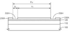
도 1c를 참조하면, 상기 포토레지스트막(130)에 대하여 소정의 패턴 형상으로 노광 및 현상하여 상기 유기 가이드층(120)을 일부 노출시키는 포토레지스트 패턴(130A)을 형성한다.Referring to FIG. 1C, a
상기 포토레지스트 패턴(130A)이 형성된 후, 상기 포토레지스트 패턴(130A)에 형성된 개구(130H)를 통해 상기 유기 가이드층(120)의 일부가 노출된다.After the
상기 포토레지스트 패턴(130A)의 개구(130H)는 그 평면 형상이 직선, 곡선, 또는 적어도 1 개의 절곡점을 가지는 선형 라인으로 될 수 있다. 또는 상기 포토레지스트 패턴(130A)의 개구(130H)는 그 평면 형상이 상기 기판(100)상의 소정의 위치를 중심으로 하는 원형 라인 또는 타원형 라인으로 될 수 있다.The
상기 포토레지스트 패턴(130A)의 개구(130H)는 제1 폭(X)을 가진다. 그리고, 상기 유기 가이드층(120)은 상호 인접한 2 개의 개구(130H) 사이에서 상기 포토레지스트 패턴(130A)에 의해 제2 폭(Y) 만큼 덮이게 된다. 여기서, 상기 제1 폭(X) 및 제2 폭(Y)은 수학식 1의 관계를 가질 수 있다.The
수학식 1에서, n은 양의 정수이다. n은 후속 공정에서 사용되는 블록 공중합체의 종류 및 분자량과 상기 개구(130h)의 폭의 크기에 따라 사용자에 의해 임의로 결정되는 수이다. 본 예에서는 n = 1인 경우를 예로 들어 설명한다.In Equation (1), n is a positive integer. n is a number arbitrarily determined by the user depending on the kind and molecular weight of the block copolymer used in the subsequent process and the width of the opening 130h. In this example, the case where n = 1 will be described as an example.
상기 포토레지스트 패턴(130A)은 통상의 포토리소그래피 공정에서의 해상 한계 이내에서 구현될 수 있는 폭을 가지도록 형성될 수 있다. 또는, 상기 포토레지스트 패턴(130A)은 통상의 포토리소그래피 공정에서의 해상 한계 이내에서 구현 가능한 소정의 폭을 가지는 포토레지스트 패턴을 형성한 후, 상기 포토레지스트 패턴에 대하여 열적 플로우(thermal flow) 또는 CAP (chamically attachment) 공정을 행하여 상기 포토레지스트 패턴의 개구 폭을 축소시켜 얻어질 수 있다.The
상기 포토레지스트 패턴(130A)에서 상기 개구(130H)는 제1 피치(PX)로 반복 형성될 수 있다.The
도 1d를 참조하면, 상기 포토레지스트 패턴(130A) 및 유기 가이드층(120)의 노출 부분 위에 블록 공중합체를 포함하는 물질층(140)을 형성한다.Referring to FIG. 1D, a
상기 물질층(140)을 형성하기 위하여 스핀코팅 공정을 이용할 수 있다.A spin coating process may be used to form the
상기 물질층(140)은 적어도 2 개의 폴리머 블록으로 이루어지는 블록 공중합체를 포함할 수 있다. 예를 들면, 상기 물질층(140) 내의 블록 공중합체는 제1 폴리머 블록 및 제2 폴리머 블록이 1:1의 부피비로 공유 결합된 블록 공중합체로 이 루어질 수 있다. 또한, 상기 블록 공중합체는 2 종류의 블록 공중합체 (A, B)로 이루어지는 2중(AB) 공중합체, 2 종류의 블록 공중합체 (A, B)로 이루어지는 3중(ABA) 공중합체, 3 종류의 블록 공중합체 (A, B, C)로 이루어지는 3중(ABC) 공중합체, 또는 다중 공중합체 (multi-component block copolymer)로 이루어질 수 있다. 상기 블록 공중합체는 약 3,000 ∼ 2,000,000 g/mol의 분자량을 가지는 선형 또는 분기형 고분자로 이루어질 수 있다.The
예를 들면, 상기 블록 공중합체가 제1 폴리머 블록 및 제2 폴리머 블록으로 이루어지는 2중 공중합체인 경우, 상기 블록 공중합체로서 폴리스티렌-폴리메틸메타크릴레이트 (polystyrene-polymethylmethacrylate) 공중합체, 폴리부타디엔-폴리부틸메타크릴레이트 (polybutadiene-polybutylmethacrylate) 공중합체, 폴리부타디엔-폴리디메틸실록산 (polybutadiene-polydimethylsiloxane) 공중합체, 폴리부타디엔-폴리메텔메타크릴레이트 (polybutadiene-polymethylmethacrylate) 공중합체, 폴리부타디엔-폴리비닐피리딘 (polybutadiene-polyvinylpyridine) 공중합체, 폴리부틸아크릴레이트-폴리메틸메타크릴레이트 (polybutylacrylate-polymethylmethacrylate), 폴리부틸아크릴레이트-폴리비닐피리딘 (polybutylacrylate-polyvinylpyridine), 폴리이소프렌-폴리비닐피리딘 (polyisoprene-polyvinylpyridine), 폴리이소프렌-폴리메틸메타크릴레이트 (polyisoprene-polymethylmethacrylate), 폴리헥실아크릴레이트-폴리비닐피리딘 (polyhexylacrylate-polyvinylpyridine), 폴리이소부틸렌-폴리부틸메타크릴레이트 (polyisobutylene-polybutylmethacrylate), 폴리이소부틸렌-폴리메틸메타크릴레이 트 (polyisobutylene-polymethylmethacrylate), 폴리이소부틸렌-폴리부틸메타크릴레이트 (polyisobutylene-polybutylmethacrylate), 폴리이소부틸렌-폴리디메틸실록산 (polyisobutylene-polydimethylsiloxane), 폴리부틸메타크릴레이트-폴리부틸아크릴레이트 (polybutylmethacrylate-polybutylacrylate), 폴리에틸에틸렌-폴리메틸메타크릴레이트 (polyethylethylene-polymethylmethacrylate), 폴리스티렌-폴리부틸메타크릴레이트 (polystyrene-polybutylmethacrylate), 폴리스티렌-폴리부타디엔 (polystyrene-polybutadiene), 폴리스티렌-폴리이소프렌 (polystyrene-polyisoprene), 폴리스티렌-폴리메틸실록산 (polystyrene-polydimethylsiloxane), 폴리스티렌-폴리비닐피리딘 (polystyrene-polyvinylpyridine), 폴리에틸에틸렌-폴리비닐피리딘 (polyethylethylene-polyvinylpyridine), 폴리에틸렌-폴리비닐피리딘 (polyethylene-polyvinylpyridine), 폴리비닐피리딘-폴리메틸메타크릴레이트 (polyvinylpyridine-polymethylmethacrylate), 폴리에틸렌옥사이드-폴리이소프렌 (polyethyleneoxide-polyisoprene), 폴리에틸렌옥사이드-폴리부타디엔 (polyethyleneoxide-polybutadiene), 폴리에틸렌옥사이드-폴리스티렌 (polyethyleneoxide-polystyrene), 폴리에틸렌옥사이드-폴리메틸메타크릴레이트 (polyethyleneoxide-polymethylmethacrylate), 폴리에틸렌옥사이드-폴리디메틸실록산 (polyethyleneoxide-polydimethylsiloxane), 폴리스티렌-폴리에틸렌옥사이드 (polystyrene-polyethyleneoxide) 등을 사용할 수 있다.For example, when the block copolymer is a double copolymer composed of the first polymer block and the second polymer block, the block copolymer may be a polystyrene-polymethylmethacrylate copolymer, a polybutadiene-poly Polybutadiene-polybutylmethacrylate copolymers, polybutadiene-polydimethylsiloxane copolymers, polybutadiene-polymethylmethacrylate copolymers, polybutadiene-polybutylmethacrylate copolymers, polybutadiene- polyvinylpyridine) copolymer, polybutylacrylate-polymethylmethacrylate, polybutylacrylate-polyvinylpyridine, polyisoprene-polyvinylpyridine, polyisoprene-polyvinylpyridine, - Polymethylmethacrylate polyisoprene-polymethylmethacrylate, polyhexylacrylate-polyvinylpyridine, polyisobutylene-polybutylmethacrylate, polyisobutylene-polybutylmethacrylate, polyisobutylene- polymethylmethacrylate, polyisobutylene-polybutylmethacrylate, polyisobutylene-polydimethylsiloxane, polybutylmethacrylate-polybutylacrylate, polyisobutylene-polydimethylsiloxane, But are not limited to, ethylethylene-polymethylmethacrylate, polystyrene-polybutylmethacrylate, polystyrene-polybutadiene, polystyrene-polyisoprene, polystyrene- Polystyrene-polydimethylsiloxane polyvinylpyridine, polystyrene-polyvinylpyridine, polyethylethylene-polyvinylpyridine, polyethylene-polyvinylpyridine, polyvinylpyridine-polymethylmethacrylate, polyvinylpyridine- polymethylmethacrylate, polyethyleneoxide-polyisoprene, polyethyleneoxide-polybutadiene, polyethyleneoxide-polystyrene, polyethyleneoxide-polymethylmethacrylate, polyethylene Polyethyleneoxide-polydimethylsiloxane, polystyrene-polyethyleneoxide, or the like can be used.
또 다른 예로서, 상기 블록 공중합체가 제1 폴리머 블록 및 제2 폴리머 블록으로 이루어지는 3중 공중합체인 경우, 상기 블록 공중합체로서 폴리스티렌-폴리메 틸메타크릴레이트-폴리스티렌 (polystyrene-polymethylmethacrylate-polystyrene) 공중합체, 폴리부타디엔-폴리부틸메타크릴레이트-폴리부타디엔 (polybutadiene-polybutylmethacrylate-polybutadiene) 공중합체, 폴리부타디엔-폴리디메틸실록산-폴리부타디엔 (polybutadiene-polydimethylsiloxane-polybutadiene) 공중합체, 폴리부타디엔-폴리메텔메타크릴레이트-폴리부타디엔 (polybutadiene-polymethylmethacrylate-polybutadiene) 공중합체, 폴리부타디엔-폴리비닐피리딘-폴리부타디엔 (polybutadiene-polyvinylpyridine-polybutadiene) 공중합체, 폴리부틸아크릴레이트-폴리메틸메타크릴레이트-폴리부틸아크릴레이트 (polybutylacrylate-polymethylmethacrylate-polybutylacrylate), 폴리부틸아크릴레이트-폴리비닐피리딘-폴리부틸아크릴레이트 (polybutylacrylate-polyvinylpyridine-polybutylacrylate), 폴리이소프렌-폴리비닐피리딘-폴리이소프렌 (polyisoprene-polyvinylpyridine-polyisoprene), 폴리이소프렌-폴리메틸메타크릴레이트-폴리이소프렌 (polyisoprene-polymethylmethacrylate-polyisoprene), 폴리헥실아크릴레이트-폴리비닐피리딘-폴리헥실아크릴레이트 (polyhexylacrylate-polyvinylpyridine-polyhexylacrylate), 폴리이소부틸렌-폴리부틸메타크릴레이트-폴리이소부틸렌 (polyisobutylene-polybutylmethacrylate-polyisobutylene), 폴리이소부틸렌-폴리메틸메타크릴레이트-폴리이소부틸렌 (polyisobutylene-polymethylmethacrylate-polyisobutylene), 폴리이소부틸렌-폴리부틸메타크릴레이트-폴리이소부틸렌 (polyisobutylene-polybutylmethacrylate-polyisobutylene), 폴리이소부틸렌-폴리디메틸실록산-폴리이소부틸렌 (polyisobutylene- polydimethylsiloxane-polyisobutylene), 폴리부틸메타크릴레이트-폴리부틸아크릴레이트-폴리부틸메타크릴레이트 (polybutylmethacrylate-polybutylacrylate-polybutylmethacrylate), 폴리에틸에틸렌-폴리메틸메타크릴레이트-폴리에틸에틸렌 (polyethylethylene-polymethylmethacrylate-polyethylethylene), 폴리스티렌-폴리부틸메타크릴레이트-폴리스티렌 (polystyrene-polybutylmethacrylate-polystyrene), 폴리스티렌-폴리부타디엔-폴리스티렌 (polystyrene-polybutadiene-polystyrene), 폴리스티렌-폴리이소프렌-폴리스티렌 (polystyrene-polyisoprene-polystyrene), 폴리스티렌-폴리메틸실록산-폴리스티렌 (polystyrene-polydimethylsiloxane-polystyrene), 폴리스티렌-폴리비닐피리딘-폴리스티렌 (polystyrene-polyvinylpyridine-polystyrene), 폴리에틸에틸렌-폴리비닐피리딘-폴리에틸에틸렌 (polyethylethylene-polyvinylpyridine-polyethylethylene), 폴리에틸렌-폴리비닐피리딘-폴리에틸렌 (polyethylene-polyvinylpyridine-polyethylene), 폴리비닐피리딘-폴리메틸메타크릴레이트-폴리비닐피리딘 (polyvinylpyridine-polymethylmethacrylate-polyvinylpyridine), 폴리에틸렌옥사이드-폴리이소프렌-폴리에틸렌옥사이드 (polyethyleneoxide-polyisoprene-polyethyleneoxide), 폴리에틸렌옥사이드-폴리부타디엔-폴리에틸렌옥사이드 (polyethyleneoxide-polybutadiene-polyethyleneoxide), 폴리에틸렌옥사이드-폴리스티렌-폴리에틸렌옥사이드 (polyethyleneoxide-polystyrene-polyethyleneoxide), 폴리에틸렌옥사이드-폴리메틸메타크릴레이트-폴리에틸렌옥사이드 (polyethyleneoxide-polymethylmethacrylate-polyethyleneoxide), 폴리에틸렌옥사이드-폴리디메틸실록 산-폴리에틸렌옥사이드 (polyethyleneoxide-polydimethylsiloxane-polyethyleneoxide), 폴리스티렌-폴리에틸렌옥사이드-폴리스티렌 (polystyrene-polyethyleneoxide-polystyrene) 등을 사용할 수 있다.As another example, when the block copolymer is a ternary copolymer comprising a first polymer block and a second polymer block, polystyrene-polymethylmethacrylate-polystyrene (hereinafter abbreviated as polystyrene-polymethylmethacrylate-polystyrene) Polybutadiene-polybutylmethacrylate-polybutadiene copolymer, polybutadiene-polydimethylsiloxane-polybutadiene copolymer, polybutadiene-polymethacrylate-polybutadiene copolymer, polybutadiene- Polybutadiene-polymethylmethacrylate-polybutadiene copolymers, polybutadiene-polyvinylpyridine-polybutadiene copolymers, polybutylacrylate-polybutylacrylate-polybutadiene copolymers, polymethylmethacrylate-polybutylacrylate), Polyisoprene-polyvinylpyridine-polyisoprene, polyisoprene-polymethylmethacrylate-polyisoprene (polyisoprene-polyvinylpyridine-polybutylene terephthalate), polybutylene terephthalate polyisoprene-polymethylmethacrylate-polyisoprene, polyhexylacrylate-polyvinylpyridine-polyhexylacrylate, polyisobutylene-polybutylmethacrylate-polyisobutylene, Polyisobutylene-polymethylmethacrylate-polyisobutylene, polyisobutylene-polybutylmethacrylate-polyisobutylene, polyisobutylene-polyisobutylene, polyisobutylene- The use of a poly-dimethyl-siloxane-polyisobutyl polybutylmethacrylate-polybutylacrylate-polybutylmethacrylate, polyethylethylene-polymethylmethacrylate-polyethyleneterephthalate, polyethylmethacrylate-polyisobutylene, ), Polystyrene-polybutylmethacrylate-polystyrene, polystyrene-polybutadiene-polystyrene, polystyrene-polyisoprene-polystyrene, polystyrene- Polystyrene-polyvinylpyridine-polystyrene, polystyrene-polydimethylsiloxane-polystyrene, polystyrene-polyvinylpyridine-polystyrene, polyethylethylene-polyvinylpyridine-polyethylethylene, But are not limited to, polyethylene-polyvinylpyridine-polyethylene, polyvinylpyridine-polymethylmethacrylate-polyvinylpyridine, polyethyleneoxide-polyisoprene-polyethyleneoxide, polyethylene oxide Polyethylene oxide-polybutadiene-polyethyleneoxide, polyethyleneoxide-polystyrene-polyethyleneoxide, polyethyleneoxide-polymethylmethacrylate-polyethyleneoxide, polyethylene oxide-polybutadiene- - Polydimethylsiloxane - Polyethyleneoxide - polydimethylsiloxane - polyethyleneoxide, polystyrene - polyethyleneoxide - polystyrene etc. Are used. can do.
그러나, 본 발명에서 사용 가능한 블록 공중합체가 상기 예시된 것들에만 제한되는 것은 아니며, 본 발명의 사상의 범위 내에서 다양한 블록 공중합체들을 사용할 수 있다.However, the block copolymers usable in the present invention are not limited to those exemplified above, and various block copolymers can be used within the scope of the present invention.
또는, 상기 물질층(140)은 제1 폴리머 블록 및 제2 폴리머 블록이 1:1의 부피비로 공유 결합된 블록 공중합체와, 상기 제1 폴리머 블록과 동일한 반복 단위를 가지는 제1 호모폴리머와, 상기 제2 폴리머 블록과 동일한 반복 단위를 가지는 제2 호모폴리머를 포함할 수 있다. 예를 들면, 상기 물질층(140) 내의 블록 공중합체가 폴리스티렌(PS)-폴리메틸메타크릴레이트(PMMA) 블록 공중합체인 경우, 상기 물질층(140)은 제1 호모폴리머로서 PS와, 상기 제2 호모폴리머로서 PMMA를 각각 더 포함할 수 있다. 상기 물질층(140) 내에서 상기 제1 호모폴리머와 제2 호모폴리머의 첨가량을 동일하게 할 수 있다. 상기 제1 호모폴리머 및 제2 호모폴리머는 각각 상기 블록 공중합체의 중량을 기준으로 0 ∼ 60 중량%의 양으로 첨가될 수 있다.Alternatively, the
분자량이 약 500 ∼ 7,000 g/mol인 제1 호모폴리머 및 제2 호모폴리머를 상기 블록 코폴리머에 첨가하는 경우에는 이들 호모폴리머를 첨가하지 않는 경우에 비해 후속 공정에서 블록 공중합체가 상분리를 통해 재배열되어 하부 막 위에 자기조립 구조를 형성할 때, 상기 자기조립 구조 형성에 필요한 시간을 단축시킬 수 있다. 또한, 분자량이 약 500 ∼ 1,000,000 g/mol인 제1 호모폴리머 및 제2 호모폴리 머를 상기 블록 코폴리머에 첨가하는 경우에는 이들 호모폴리머를 첨가하지 않는 경우에 비해 후속 공정에서 블록 공중합체가 자기조립 구조를 형성할 때, 상기 자기조립 구조의 피치를 증가시킬 수 있다. 따라서, 상기 제1 호모폴리머 및 제2 호모폴리머의 분자량 및 첨가량을 조절함으로써 원하는 피치를 가지는 자기조립 구조를 형성할 수 있다.When the first homopolymer and the second homopolymer having a molecular weight of about 500 to 7,000 g / mol are added to the block copolymer, the block copolymer in the subsequent step, When the self-assembled structure is formed on the lower film, the time required for forming the self-assembled structure can be shortened. In addition, when the first homopolymer and the second homopolymer having a molecular weight of about 500 to 1,000,000 g / mol are added to the block copolymer, the amount of the block copolymer in the subsequent step When forming the assembled structure, the pitch of the self assembled structure can be increased. Therefore, the self-assembled structure having a desired pitch can be formed by controlling the molecular weight and addition amount of the first homopolymer and the second homopolymer.
도 1e를 참조하면, 상기 물질층(140)의 상분리를 통해 상기 물질층(140)의 성분들을 재배열시켜 서로 다른 성분의 모노머 유니트로 이루어지는 복수의 제1 블록(140A) 및 복수의 제2 블록(140B)을 포함하는 미세 패턴층(140C)을 형성한다.Referring to FIG. 1E, the material layers 140 are rearranged through phase separation of the
복수의 제1 블록(140A) 및 복수의 제2 블록(140B)은 이들을 구성하는 폴리머의 반복 단위의 구조에 따라 극성이 서로 다르다. 또한, 상기 유기 가이드층(140)은 친수성 기를 가지는 폴리머 블록인 제1 블록(140A)에 대한 친화도가 크다. 반면, 포토레지스트 패턴(130A)은 친수성 기를 가지는 폴리머 블록과 소수기를 가지는 폴리머 블록중 어느 쪽에도 선택성을 가지지 않는다.The plurality of first blocks 140A and the plurality of
상기 물질층(140)에서 상분리된 블록 공중합체의 폴리머 블록들은 그들이 포함하고 있는 친수성 기에 따라 서로 다른 극성을 가지고 있다. 상기 유기 가이드층(140)은 상기 폴리머 블록들 중 친수성 또는 극성이 더 큰 폴리머 블록에 대하여 친화도를 가지므로, 포토레지스트 패턴(130A)을 통해 노출되는 유기 가이드층(140)은 친수성 또는 극성이 더 큰 폴리머 블록, 즉 제1 블록(140A)을 가이드하는 역할을 하여 상기 제1 블록(140A)이 유기 가이드층(140)의 노출 부분 위에 자기정렬되어 어드레싱(addressing)된다. 반면, 상기 포토레지스트 패턴(130A)은 친수성 기를 가지는 폴리머 블록과 소수기를 가지는 폴리머 블록중 어느 쪽에도 선택성을 가지지 않으므로, 상기 포토레지스트 패턴(130A)상에서는 폴리머 블록들이 수직으로 배향한다. 그 결과, 상기 유기 가이드층(140)의 노출 부분 위에 어드레싱된 제1 블록(140A)을 기준으로 하여 포토레지스트 패턴(130A)상에서 물질층(140) 내에 있는 폴리머 블록들이 수직으로 배향하면서 상기 유기 가이드층(140)의 노출 부분 위에 어드레싱된 제1 블록(140A)에 이어서 제2 블록(140B), 제1 블록(140A)의 순서로 상기 포토레지스트 패턴(130A) 위에 교대로 반복 배치되어 패턴 멀티플라잉 (pattern multiplying)이 일어나게 된다.The polymer blocks of the block copolymer phase-separated in the
상기 물질층(140)의 상분리를 통해 상기 물질층(140)의 성분들을 재배열시키기 위하여, 상기 물질층(140) 내의 블록 공중합체의 유리전이온도(Tg_BC) 보다 더 높은 온도하에서 상기 물질층(140)을 어닐링한다. 예를 들면, 상기 물질층(140)을 상분리하기 위하여 약 100 ∼ 190 ℃의 범위 내에서 선택되는 온도하에서 약 1 ∼ 24 시간 동안 상기 물질층(140)을 어닐링할 수 있다. 이 때, 상기 물질층(140)의 어닐링은 상기 물질층(140) 내의 블록 공중합체의 유리전이온도(Tg_BC) 보다는 더 높고 상기 포토레지스트 패턴(130A)의 유리전이온도(Tg_PR) 보다는 더 낮은 온도에서 행해질 수 있다. 그 이유는 상기 물질층(140)의 어닐링시 상기 포토레지스트 패턴(130A)이 열에 의해 플로우되어 형태가 변형될 수 있는 가능성을 제거하기 위함이다. 상기 물질층(140) 내의 블록 공중합체의 유리전이온도(Tg_BC)는 상기 블록 공중합체의 분자량에 따라 달라질 수 있다. 그러나, 상기 물질층(140)의 어닐링이 포토레지스트 패턴(130A)의 유리전이온도 (Tg_PR) 이상의 온도에서 행해지는 경우 에도, 상기 물질층(140)의 어닐링에 의해 형성된 미세 패턴층(140C)을 구성하는 제1 블록(140A)이 포토레지스트 패턴(130A)의 개구(130H)를 통해 노출된 유기 가이드층(120) 위에 자기정렬된 상태에서 상기 포토레지스트 패턴(130A)의 개구(130H)를 채우고 있으므로, 포토레지스트 패턴(130A)의 열적 플로우에 의한 플로우 거리가 상기 제1 블록(140A)에 의해 제한된다. 따라서, 포토레지스트 패턴(130A)의 열적 플로우가 상기 미세 패턴층(140A)에 미치는 영향은 무시할 만 하다.(Tg_BC) of the block copolymer in the material layer (140) to rearrange the components of the material layer (140) through phase separation of the material layer (140) 140 are annealed. For example, the
상기 물질층(140)의 상분리를 통해 상기 물질층(140)의 성분들을 재배열시키기 위한 다른 방법으로서, 상기 물질층(140)이 형성된 결과물을 톨루엔 증기(vapor)로 포화된 분위기로 유지되는 챔버 내에서 소정 시간 동안 유지시키는 공정을 이용할 수도 있다.As another method for rearranging the components of the
상기 물질층(140) 내의 블록 공중합체를 구성하는 폴리머 블록들중에서 극성이 더 큰 폴리머 블록이 상기 유기 가이드층(120)의 노출 부분 위에 자기정렬되어 상기 유기 가이드층(120)의 노출 부분을 덮게 된다. 그리고, 상기 포토레지스트 패턴(120) 위에서는 상기 블록 공중합체의 분자량 및 상기 유기 가이드층(120)의 노출 부분의 폭(X)에 따라 상기 제1 폴리머 블록 및 제2 폴리머 블록이 각각 균일한 폭을 가지고 등간격으로 교대로 반복 배치되도록 수직으로 배향된다.A polymer block having a higher polarity among the polymer blocks constituting the block copolymer in the
예를 들면, 상기 물질층(140) 내의 블록 공중합체의 제1 폴리머 블록 및 제2 폴리머 블록중 제1 폴리머 블록의 극성이 더 큰 경우, 도 1e에 예시된 바와 같이 상기 제1 폴리머 블록이 상기 유기 가이드층(120)의 노출 부분 위에 자기정렬됨으로써 상기 제1 블록(140A)을 형성하게 된다. 상기 제1 블록(140A)은 상기 유기 가 이드층(120)의 노출 부분을 가이드로 하여 상기 유기 가이드층(120) 및 포토레지스트 패턴(130A)의 노출 표면에 등간격으로 일정한 폭을 가지고 반복적으로 배열된다. 그리고, 상기 제2 폴리머 블록은 상기 제1 폴리머 블록과 동일한 폭을 가지고 상기 제1 폴리머 블록과 교대로 배치되는 형상으로 상기 포토레지스트 패턴(130A) 위에 자기정렬됨으로써 상기 제2 블록(124B)을 형성하게 된다. 여기서, 상기 제1 블록(140A) 및 제2 블록(140B)의 배열 구조에 의해 상기 미세 패턴층(140C)에서 소정의 형상을 가지는 패턴이 형성된다.For example, if the first polymer block of the block copolymer and the first polymer block of the block copolymer in the
예를 들면, 상기 물질층(140) 내의 블록 공중합체가 폴리스티렌(PS)-폴리메틸메타크릴레이트(PMMA) 블록 공중합체인 경우, 포토레지스트 패턴(130A)에 비해 극성이 더 큰 유기 가이드층(120)의 노출 부분에 어드레싱되는 제1 블록(140A)은 상대적으로 친수성이 큰 PMMA로 이루어지고, 상기 제2 블록(140B)은 PS로 이루어질 수 있다.For example, when the block copolymer in the
상기 미세 패턴층(140C)에서 상기 제1 블록(140A)은 포토레지스트 패턴(130A)의 개구(130H)의 제1 폭(X)과 동일한 폭(X)을 가질 수 있다. 그리고, 상기 제1 블록(140A)은 상기 제1 피치(Px) 보다 작은 제2 피치(PBC)로 반복 배치될 수 있다.In the
상기 제1 블록(140A)이 포토레지스트 패턴(130A)의 개구(130H)의 제1 폭(X)과 동일한 폭(X)을 가지고, 포토레지스트 패턴(130A)의 제2 폭(Y)이 수학식 1로 표시될 때, 상기 제2 피치(PBC)는 수학식 2로 표시될 수 있다.The first block 140A has a width X equal to the first width X of the
예를 들면, n = 1인 경우, 상기 제2 피치(PBC)는 상기 제1 피치(Px) 보다 1/2 배 축소된 피치를 가진다.For example, when n = 1, the second pitch PBC has a pitch that is 1/2 times smaller than the first pitch Px.
상기 물질층(140)이 제1 폴리머 블록 및 제2 폴리머 블록으로 이루어지는 블록 공중합체와, 상기 제1 폴리머 블록과 동일한 반복 단위로 구성되는 제1 호모 폴리머와, 상기 제2 폴리머 블록과 동일한 반복 단위로 구성되는 제2 호모폴리머로 구성되는 경우, 상기 제1 블록(140A)은 보다 극성이 큰 상기 제1 폴리머 블록 및 제1 호모폴리머가 상기 유기 가이드층(120)의 노출 부분 위에 자기정렬되어 형성된다. 상기 제1 블록(140A)은 상기 유기 가이드층(120)의 노출 부분을 가이드로 하여 상기 유기 가이드층(120)의 노출 부분 및 포토레지스트 패턴(130A) 위에 등간격으로 일정한 폭을 가지고 반복적으로 배열된다. 상기 제2 블록(140B)은 비교적 극성이 작은 제2 폴리머 블록 및 제2 호모폴리머가 상기 제1 블록(140A)과 교대로 상기 포토레지스트 패턴(130A) 위에 자기정렬되어 형성된다. 상기 물질층(140)에 상기 제1 호모폴리머 및 제2 호모폴리머를 첨가함으로써 이들을 첨가하지 않는 경우에 비해 상기 미세 패턴층(140C)의 형성 시간을 단축할 수 있으며, 이들을 첨가하지 않는 경우에 비해 상기 제2 피치(PBC)를 크게 할 수 있다.Wherein the material layer (140) comprises a block copolymer comprising a first polymer block and a second polymer block, a first homopolymer comprising the same repeating unit as the first polymer block, and a second homopolymer comprising the same repeating unit as the second polymer block The first block 140A is formed by self-aligning the first polymer block and the first homopolymer having a higher polarity on the exposed portion of the
도 1f를 참조하면, 상기 미세 패턴층(140C)에서 상기 복수의 제1 블록(140A) 및 복수의 제2 블록(140B) 중 어느 하나를 제거하여 미세 패턴 마스크(140D)를 형 성한다. 도 1f에는 상기 복수의 제1 블록(140A)을 제거하여 상기 유기 가이드층(120)의 노출 부분과 상기 포토레지스트 패턴(130A)의 상면중 일부를 노출시키는 미세 패턴 마스크(140D)를 형성한 경우를 예시하였다. 그러나, 본 발명은 이에 한정되는 것은 아니며, 상기 복수의 제2 블록(140B)을 제거하여 상기 미세 패턴 마스크(140D)를 형성할 수도 있다. 이 경우에도 본 발명에 따른 효과를 동일하게 얻을 수 있다.Referring to FIG. 1F, a
상기 복수의 제1 블록(140A) 및 복수의 제2 블록(140B) 중 어느 하나를 제거하기 위하여, 예를 들면 제거하고자 하는 블록에 UV를 조사하거나 산소 플라즈마에 노출시켜 광분해시킨 후, 광분해된 부분을 세정액으로 스트립하는 공정을 이용할 수 있다.In order to remove either the first block 140A or the
도 1g를 참조하면, 상기 미세 패턴 마스크(140D)를 식각 마스크로 하여 상기 유기 가이드층(120)의 노출 부분과 포토레지스트 패턴(130A)의 노출 부분 및 그 하부의 유기 가이드층(120)을 식각하고, 이어서 상기 미세 패턴 마스크(140D)를 식각 마스크로 하여 상기 피식각막(110)을 식각하여 원하는 미세 패턴(110A)을 형성한다.Referring to FIG. 1G, the exposed portion of the
상기 피식각막(110)의 형성을 생략한 경우, 상기 미세 패턴 마스크(140D)를 식각 마스크로 하여 상기 기판(100)을 식각하여 원하는 미세 패턴을 형성할 수도 있다.If the
도 1h를 참조하면, 상기 미세 패턴 마스크(140D)를 제거하고, 상기 미세 패턴(110A) 상부에 남아 있는 불필요한 막들을 제거한다.Referring to FIG. 1H, the
상기 미세 패턴(110A)은 상기 포토레지스트 패턴(130A)의 개구(130H)를 통해 노출되는 유기 가이드층(120)의 노출 부분에 의해 형성되는 패턴의 제1 피치(Px)에 비해 1/2 배 축소된 제2 피치(PBC)와 동일한 피치로 반복 형성될 수 있다. 따라서, 상기 미세 패턴(110A)은 상기 유기 가이드층(120)의 노출 부분에 의해 형성되는 패턴 밀도에 비해 2 배 증가된 패턴 밀도를 가진다.The
도 1a 내지 도 1h를 참조하여 설명한 제1 실시예에 따른 미세 패턴 형성 방법에서는 n = 1인 경우를 예시하여 설명하였으나, 본 발명은 n = 2, 3, 4, ...인 경우에도 동일하게 적용할 수 있음은 물론이다.In the method of forming a fine pattern according to the first embodiment described with reference to FIGS. 1A to 1H, n = 1 is exemplified and the present invention is also applicable to the case of n = 2, 3, 4, Of course, can be applied.
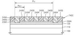
도 2a 내지 도 2d는 본 발명의 제2 실시예에 따른 미세 패턴 형성 방법을 설명하기 위하여 공정 순서에 따라 도시한 단면도들이다.2A to 2D are cross-sectional views illustrating a method of forming a fine pattern according to a second embodiment of the present invention.
도 2a 내지 도 2d를 참조하여 설명하는 본 발명의 제2 실시예서는 n = 3 인 경우를 예시한 것을 제외하고 제1 실시예에서와 대체로 동일하다. 도 2a 내지 도 2d에 있어서, 도 1a 내지 도 1h에서와 동일한 참조 부호는 동일 부재를 나타내며, 따라서 본 예에서는 이들에 대한 상세한 설명은 생략한다.The second embodiment of the present invention described with reference to Figs. 2A to 2D is substantially the same as the first embodiment except that n = 3 is exemplified. In Figs. 2A to 2D, the same reference numerals as in Figs. 1A to 1H denote the same members, and therefore, a detailed description thereof will be omitted in this embodiment.
도 2a를 참조하면, 도 1a 내지 도 1c를 참조하여 설명한 바와 같은 방법으로 기판(100)상에 피식각막(110) 및 유기 가이드층(120)을 차례로 형성한 후, 상기 유기 가이드층(120) 위에 상기 유기 가이드층(120)을 일부 노출시키는 포토레지스트 패턴(230A)을 형성한다.2A, after the
상기 포토레지스트 패턴(130A)의 구성 재료는 도 1b를 참조하여 포토레지스 트막(130)에 대하여 설명한 바와 같다.The constituent material of the
n = 3인 경우의 수학식 1에 따라, 상기 포토레지스트 패턴(230A)의 폭(Y2)이 상기 포토레지스트 패턴(230A)에 형성된 복수의 개구(230H)의 폭(X2)의 7 배이다. 상기 포토레지스트 패턴(230A)에서 상기 개구(230H)는 제1 피치(PX2)로 반복 형성될 수 있다.the width Y2 of the
도 2b를 참조하면, 도 1d 및 도 1e를 참조하여 설명한 바와 같은 방법으로 상기 포토레지스트 패턴(230A) 위에 블록 공중합체를 포함하는 물질층(140)을 형성한 후, 상기 물질층(140)의 상분리를 통해 상기 물질층(140)의 성분들을 재배열시켜 서로 다른 성분의 모노머 유니트로 이루어지는 복수의 제1 블록(240A) 및 복수의 제2 블록(240B)을 포함하는 미세 패턴층(240C)을 형성한다.Referring to FIG. 2B, a
예를 들면, 상기 물질층(140) 내의 블록 공중합체가 폴리스티렌(PS)-폴리메틸메타크릴레이트(PMMA) 블록 공중합체인 경우, 극성인 유기 가이드층(120)의 노출 부분에 자기조립되어 어드레싱되는 상기 제1 블록(240A)은 친수성이 비교적 큰 PMMA로 이루어지고, 상기 제2 블록(240B)은 PS로 이루어질 수 있다.For example, when the block copolymer in the
상기 복수의 제1 블록(240A) 및 복수의 제2 블록(240B)을 포함하는 미세 패턴층(240C)에 대한 구체적인 구성은 제1 실시예에서의 복수의 제1 블록(140A) 및 복수의 제2 블록(140B)을 포함하는 미세 패턴층(140C)과 대체로 동일하다. 단, n = 3인 경우의 수학식 2에 따라, 상기 미세 패턴층(240C)에서 상기 제1 블록(240A) 및 제2 블록(240B) 각각의 피치(PBC2)는 제1 피치(PX2)의 1/4로 축소되어 상기 미세 패 턴층(240C)에서의 패턴 밀도가 상기 포토레지스트 패턴(230A)에서의 패턴 밀도 보다 4 배 증가한다.The detailed structure of the
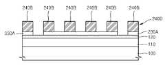
도 2c를 참조하면, 도 1f를 참조하여 미세 패턴층(140C)에 대하여 설명한 바와 같은 방법으로 상기 미세 패턴층(240C)에서 상기 복수의 제1 블록(240A) 및 복수의 제2 블록(240B) 중 어느 하나를 제거하여, 상기 유기 가이드층(120)의 일부와 상기 포토레지스트 패턴(230A)의 일부를 노출시키는 미세 패턴 마스크(240D)를 형성한다. 도 2c에는 상기 복수의 제1 블록(240A) 및 복수의 제2 블록(240B) 중 복수의 제1 블록(240A)을 제거한 경우를 예시하였다. 그러나, 본 발명을 이에 한정되는 것은 아니며, 상기 복수의 제2 블록(240B)을 제거하여 복수의 제1 블록(240A)으로 이루어지는 미세 패턴 마스크(도시 생략)를 형성할 수도 있다.Referring to FIG. 2C, the plurality of
도 2d를 참조하면, 도 1g 및 도 1h를 참조하여 설명한 바와 같은 방법으로 상기 미세 패턴 마스크(240D)를 식각 마스크로 하여 유기 가이드층(120)의 노출 부분과 포토레지스트 패턴(130A)의 노출 부분 및 그 하부의 유기 가이드층(120)을 식각하고, 이어서 상기 미세 패턴 마스크(140D)를 식각 마스크로 하여 상기 피식각막(110)을 식각하여 원하는 미세 패턴(110B)을 형성한다.Referring to FIG. 2D, the exposed portion of the
그 후, 상기 미세 패턴 마스크(240D)를 제거하고, 상기 미세 패턴(110B) 상부에 남아 있는 불필요한 막들을 제거한다.Thereafter, the
상기 미세 패턴(110B)은 상기 포토레지스트 패턴(230A)에 형성된 복수의 개구(230H)의 제1 피치(PX2) (도 2a 참조) 보다 1/4 배 축소된 제2 피치(PBC2)와 동일 한 피치를 가질 수 있다. 따라서, 상기 포토레지스트 패턴(230A)에 형성된 복수의 개구(230H)에 의해 형성되는 패턴 밀도에 비해 4 배 증가된 패턴 밀도를 얻을 수 있다.The
도 1a 내지 도 1h를 참조하여 설명한 본 발명의 제1 실시예에 따른 미세 패턴 형성 방법과, 도 2a 내지 도 2d를 참조하여 설명한 본 발명의 제2 실시예에 따른 미세 패턴 형성 방법에 의해 다양한 평면 형상을 가지는 미세 패턴을 형성할 수 있다. 예를 들면, 본 발명에 따른 미세 패턴 형성 방법에 의해 직선 또는 곡선 형상의 라인 앤드 스페이스 패턴, 적어도 1 개의 절곡점을 가지는 절곡된 형상의 선형 라인 패턴, 기판(100)상의 소정의 위치를 중심으로 하는 원형 라인 앤드 스페이스 패턴, 타원형 라인 앤드 스페이스 패턴 등 다양한 형상의 평면 구조를 가지는 패턴을 형성할 수 있다.The method of forming a fine pattern according to the first embodiment of the present invention described with reference to Figs. 1A to 1H and the method of forming a fine pattern according to the second embodiment of the present invention described with reference to Figs. 2A to 2D, A fine pattern having a shape can be formed. For example, by the method of forming a fine pattern according to the present invention, a line-and-space pattern of a straight line or a curved line, a linear line pattern of a bent shape having at least one bending point, A circular line-and-space pattern, an elliptical line-and-space pattern, and the like.
도 3은 제1 실시예에서 형성한 포토레지스트 패턴(130A)에 형성된 복수의 개구(130H)(도 1c 참조)의 평면 형상, 또는 제2 실시예에서 형성한 포토레지스트 패턴(230A)에 형성된 복수의 개구(230H)(도 2a 참조)의 평면 형상이 상호 평행하게 배치되는 복수의 라인 형상을 가지는 경우, 미세 패턴층(140C 또는 240C)(도 1e 및 도 2b 참조)의 배열 형상과 동일한 배열 형상을 가지는 미세 패턴층(340C)을 예시한 평면도이다.3 is a plan view of a plurality of
상기 미세 패턴층(340C)은 상기 개구(130H) 또는 개구(230H)를 통해 노출되는 유기 가이드층(120)의 노출 부분을 가이드 라인으로 하여 그 위에 자기조립되어 있으며, 상기 미세 패턴층(340C)의 제1 블록(340A) 및 제2 블록(340B)이 상호 평행 한 복수의 라인 형상을 가지도록 배열되어 있다. 도 3에서, 제1 블록(340A) 및 제2 블록(340B)으로 이루어지는 미세 패턴층(340C)은 제1 실시예에서의 제1 블록(140A) 및 제2 블록(140B)으로 이루어지는 미세 패턴층(140C)(도 1e 참조)에 대응될 수 있다. 또는, 상기 미세 패턴층(340C)은 제2 실시예에서의 제1 블록(240A) 및 제2 블록(240B)으로 이루어지는 미세 패턴층(240C)(도 2b 참조)에 대응될 수도 있다.The
상기 미세 패턴층(340C)이 제1 실시예에서의 미세 패턴층(140C)에 대응되는 경우, 상기 미세 패턴층(340C)에서 상기 제1 블록(340A)은 복수의 개구(130H)를 통해 노출되는 유기 가이드층(120)의 노출 부분들과 오버랩되는 복수의 제1 라인(340A1)과, 상기 복수의 개구(130H)중 상호 인접한 2 개의 개구(130H) 사이에 있는 포토레지스트 패턴(130A)의 위에서 상기 제1 라인(340A1)과 평행하게 연장되는 적어도 1개의 제2 라인(340A2)을 포함한다. 상기 제2 블록(340B)은 상기 제1 라인(340A1) 및 제2 라인(340A2) 사이에서 이들과 교대로 평행하게 배열되는 복수의 라인(340B1, 340B2)을 포함한다.When the
제1 실시예에서 n = 1 인 경우의 미세 패턴 형성 공정을 예시하고 있으므로, 포토레지스트 패턴(130A)의 폭은 상기 개구(130H)의 폭 보다 3 배 큰 폭을 가지며, 상기 포토레지스트 패턴(130A) 위에는 1 개의 제2 라인(340A2)이 형성된다.The width of the
도 4는 제1 실시예에서 형성한 포토레지스트 패턴(130A)에 형성된 복수의 개구(130H)의 평명 형상이 상호 평행하게 배치되는 복수의 라인 형상을 가지되, 적어 도 1 개의 변곡점을 가지고, 그에 따라 그 위에 형성된 미세 패턴층(340C)에도 변곡점(450)을 가지는 경우를 예시한 평면도이다. 도 4에서 상기 변곡점(450)을 가지는 것을 제외하면, 도 3의 구성과 대체로 동일하다. 도 4에서, 도 3에서와 동일한 참조 부호는 동일 부재를 나타낸다. 따라서, 본 예에서는 이들에 대한 상세한 설명은 생략한다.Fig. 4 is a cross-sectional view of a
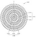
도 5는 제1 실시예에서 형성한 포토레지스트 패턴(130A)에 형성된 복수의 개구(130H)의 평명 형상이 기판(100)상의 소정의 위치(C)를 중심으로 하여 동심원상으로 반복 배치되는 복수의 원형 라인 형상을 가지는 경우, 미세 패턴층(540C)의 배열 형상을 예시한 평면도이다.5 is a plan view of a plurality of
상기 미세 패턴층(540C)은 복수의 개구(130H)를 통해 노출되는 유기 가이드층(120)의 노출 부분들을 가이드로 하여 그 위에 자기조립되어 있으며, 상기 미세 패턴층(540C)의 제1 블록(540A) 및 제2 블록(540B)이 상기 위치(C)를 중심으로 하는 동심원 형상으로 교대로 반복 배열되어 있다. 도 5에 도시된 제1 블록(540A) 및 제2 블록(540B)으로 이루어지는 미세 패턴층(540C)은 제1 실시예에서의 제1 블록(140A) 및 제2 블록(140B)으로 이루어지는 미세 패턴층(140C)에 대응될 수 있다.The
도 5에서, 상기 미세 패턴층(540C)의 상기 제1 블록(540A)은 개구(130H)를 통해 노출되는 유기 가이드층(120)의 노출 부분들과 오버랩되는 복수의 제1 원형 라인(540A1)과, 복수의 개구(130H) 중 상호 인접한 2 개의 개구(130H) 사이에 있는 포토레지스트 패턴(130H) 위에서 상기 제1 원형 라인(540A1)과 동심원 형상으로 형 성되는 적어도 1개의 제2 원형 라인(540A2)을 포함한다. 상기 제2 블록(540B)은 상기 제1 원형 라인(540A1) 및 제2 원형 라인(540A2) 사이에서 이들과 교대로 배열되는 복수의 원형 라인(540B1, 540B2)을 포함한다.In Figure 5, the microstructure of the first block of the pattern layer (540C), (540A) includes a plurality of first circular line to overlap with the exposed portion of the
제1 실시예에서 n = 1 인 경우의 미세 패턴 형성 공정을 예시하고 있으므로, 포토레지스트 패턴(130A)의 폭은 상기 개구(130H)의 폭 보다 3 배 큰 폭을 가지며, 상기 포토레지스트 패턴(130A) 위에는 1 개의 제2 원형 라인(540A2)이 형성된다.The width of the
이상, 본 발명을 바람직한 실시예를 들어 상세하게 설명하였으나, 본 발명은 상기 실시예에 한정되지 않고, 본 발명의 기술적 사상 및 범위 내에서 당 분야에서 통상의 지식을 가진 자에 의하여 여러가지 변형 및 변경이 가능하다.While the present invention has been particularly shown and described with reference to exemplary embodiments thereof, it is to be understood that the invention is not limited to the disclosed exemplary embodiments, but, on the contrary, This is possible.
도 1a 내지 도 1h는 본 발명의 제1 실시예에 따른 미세 패턴 형성 방법을 설명하기 위하여 공정 순서에 따라 도시한 단면도들이다.FIGS. 1A to 1H are cross-sectional views illustrating a method of forming a fine pattern according to a first embodiment of the present invention.
도 2a 내지 도 2d는 본 발명의 제2 실시예에 따른 미세 패턴 형성 방법을 설명하기 위하여 공정 순서에 따라 도시한 단면도들이다.2A to 2D are cross-sectional views illustrating a method of forming a fine pattern according to a second embodiment of the present invention.
도 3은 본 발명에 따른 미세 패턴 형성 방법에 의해 구현되는 제1 예에 따른 미세 패턴층의 배열 형상을 보여주는 평면도이다.3 is a plan view showing an arrangement pattern of a fine pattern layer according to a first example implemented by the method of forming a fine pattern according to the present invention.
도 4는 본 발명에 따른 미세 패턴 형성 방법에 의해 구현되는 제2 예에 따른 미세 패턴층의 배열 형상을 보여주는 평면도이다.4 is a plan view showing an arrangement pattern of a fine pattern layer according to a second example implemented by the method of forming a fine pattern according to the present invention.
도 5는 본 발명에 따른 미세 패턴 형성 방법에 의해 구현되는 제3 예에 따른 미세 패턴층의 배열 형상을 보여주는 평면도이다.5 is a plan view showing an arrangement pattern of a fine pattern layer according to a third example implemented by the method of forming a fine pattern according to the present invention.
<도면의 주요 부분에 대한 부호의 설명>Description of the Related Art
100: 기판, 110: 피식각막, 120: 유기 가이드층, 130: 포토레지스트막, 130A: 포토레지스트 패턴, 130H: 개구, 140: 물질층, 140A: 제1 블록, 140B: 제2 블록, 140C: 미세 패턴층, 140D: 미세 패턴 마스크, 110A, 110B: 미세 패턴, 230A: 포토레지스트 패턴, 230H: 개구, 240A: 제1 블록, 240B: 제2 블록, 240C: 미세 패턴층, 240D: 미세 패턴 마스크, 340A: 제1 블록, 340A1: 제1 라인, 340A2: 제2 라인, 340B: 제2 블록, 340B1, 340B2: 라인, 340C: 미세 패턴층, 450: 변곡점, 540A: 제1 블록, 540A1: 제1 원형 라인, 540A2: 제2 원형 라인, 540B: 제2 블록, 540B1, 540B2: 원형 라인, 540C: 미세 패턴층.The present invention relates to a photoresist pattern for forming a photoresist pattern on a semiconductor substrate, and more particularly, to a photoresist pattern, A first pattern and a second pattern are formed on the first pattern and the second pattern on the first pattern and the second pattern on the second pattern. 340A: first block, 340A1 : first line, 340A2 : second line, 340B: second block, 340B1 , 340B2 : line, 340C: fine pattern layer, 450: inflexion point, 540A: , 540A1 : first circular line, 540A2 : second circular line, 540B: second block, 540B1 , 540B2 : circular line, 540C: fine pattern layer.
Claims (10)
Translated fromKoreanPriority Applications (2)
| Application Number | Priority Date | Filing Date | Title |
|---|---|---|---|
| KR1020080138549AKR101535227B1 (en) | 2008-12-31 | 2008-12-31 | Method for forming fine pattern using block copolymer |
| US12/591,427US8263323B2 (en) | 2008-12-31 | 2009-11-19 | Method of forming fine pattern using block copolymer |
Applications Claiming Priority (1)
| Application Number | Priority Date | Filing Date | Title |
|---|---|---|---|
| KR1020080138549AKR101535227B1 (en) | 2008-12-31 | 2008-12-31 | Method for forming fine pattern using block copolymer |
Publications (2)
| Publication Number | Publication Date |
|---|---|
| KR20100079948A KR20100079948A (en) | 2010-07-08 |
| KR101535227B1true KR101535227B1 (en) | 2015-07-08 |
Family
ID=42285374
Family Applications (1)
| Application Number | Title | Priority Date | Filing Date |
|---|---|---|---|
| KR1020080138549AActiveKR101535227B1 (en) | 2008-12-31 | 2008-12-31 | Method for forming fine pattern using block copolymer |
Country Status (2)
| Country | Link |
|---|---|
| US (1) | US8263323B2 (en) |
| KR (1) | KR101535227B1 (en) |
Cited By (1)
| Publication number | Priority date | Publication date | Assignee | Title |
|---|---|---|---|---|
| US11251189B2 (en) | 2009-02-09 | 2022-02-15 | Longitude Flash Memory Solutions Ltd. | Gate fringing effect based channel formation for semiconductor device |
Families Citing this family (62)
| Publication number | Priority date | Publication date | Assignee | Title |
|---|---|---|---|---|
| WO2008115600A1 (en)* | 2007-03-21 | 2008-09-25 | Olambda, Inc. | Multi-material hard mask or prepatterned layer for use with multi-patterning photolithography |
| US8790262B2 (en)* | 2007-05-16 | 2014-07-29 | General Electric Company | Method for implementing an imaging and navigation system |
| KR101435520B1 (en) | 2008-08-11 | 2014-09-01 | 삼성전자주식회사 | Semiconductor device and pattern forming method of semiconductor device |
| KR101540083B1 (en) | 2008-10-22 | 2015-07-30 | 삼성전자주식회사 | Method for pattern formation of semiconductor device |
| KR101532012B1 (en)* | 2008-12-24 | 2015-06-30 | 삼성전자주식회사 | Semiconductor device and method of forming patterns for semiconductor device |
| US8821978B2 (en)* | 2009-12-18 | 2014-09-02 | International Business Machines Corporation | Methods of directed self-assembly and layered structures formed therefrom |
| US8828493B2 (en)* | 2009-12-18 | 2014-09-09 | International Business Machines Corporation | Methods of directed self-assembly and layered structures formed therefrom |
| JP5820676B2 (en) | 2010-10-04 | 2015-11-24 | ローム アンド ハース エレクトロニック マテリアルズ エルエルシーRohm and Haas Electronic Materials LLC | Lower layer composition and method for imaging lower layer |
| JP6035017B2 (en) | 2010-10-04 | 2016-11-30 | ローム アンド ハース エレクトロニック マテリアルズ エルエルシーRohm and Haas Electronic Materials LLC | Lower layer composition and method for imaging lower layer |
| NL2007940A (en) | 2010-12-23 | 2012-06-27 | Asml Netherlands Bv | Methods for providing patterned orientation templates for self-assemblable polymers for use in device lithography. |
| WO2012129162A2 (en)* | 2011-03-18 | 2012-09-27 | Cornell University | Methods of making patterned structures of materials, patterned structures of materials, and methods of using same |
| CN102915907B (en)* | 2011-08-02 | 2015-05-13 | 中芯国际集成电路制造(北京)有限公司 | Semiconductor device manufacturing method |
| JP2013174766A (en)* | 2012-02-27 | 2013-09-05 | Toshiba Corp | Mask pattern formation method, mask pattern formation program, and semiconductor device manufacturing method |
| EP2642341A2 (en)* | 2012-03-22 | 2013-09-25 | Koninklijke Philips N.V. | Manufacturing method of an apparatus for the processing of single molecules |
| JP5973763B2 (en)* | 2012-03-28 | 2016-08-23 | 東京エレクトロン株式会社 | Method and apparatus for forming periodic patterns using self-organizable block copolymers |
| KR20130120586A (en)* | 2012-04-26 | 2013-11-05 | 삼성전자주식회사 | Methods of forming a pattern |
| JP5710546B2 (en) | 2012-04-27 | 2015-04-30 | 信越化学工業株式会社 | Pattern formation method |
| JP5642731B2 (en) | 2012-04-27 | 2014-12-17 | 信越化学工業株式会社 | Pattern formation method |
| JP5816133B2 (en)* | 2012-06-04 | 2015-11-18 | 株式会社東芝 | Pattern forming method, original plate, and data processing method |
| KR102003334B1 (en)* | 2012-09-04 | 2019-07-24 | 삼성전자주식회사 | Method of forming patterns |
| US8715917B2 (en) | 2012-10-04 | 2014-05-06 | International Business Machines Corporation | Simultaneous photoresist development and neutral polymer layer formation |
| KR101477350B1 (en)* | 2012-10-23 | 2014-12-30 | 포항공과대학교 산학협력단 | Asymmetric line nanopatterns and manufacturing methods thereof |
| US9405201B2 (en)* | 2012-11-13 | 2016-08-02 | Taiwan Semiconductor Manufacturing Company, Ltd. | Lithography process using directed self assembly |
| JP6088803B2 (en)* | 2012-11-16 | 2017-03-01 | 株式会社日立ハイテクノロジーズ | Image processing apparatus, pattern generation method using self-organized lithography technology, and computer program |
| US9107291B2 (en) | 2012-11-21 | 2015-08-11 | International Business Machines Corporation | Formation of a composite pattern including a periodic pattern self-aligned to a prepattern |
| US8859433B2 (en)* | 2013-03-11 | 2014-10-14 | International Business Machines Corporation | DSA grapho-epitaxy process with etch stop material |
| WO2014139793A1 (en)* | 2013-03-15 | 2014-09-18 | Asml Netherlands B.V. | Methods for providing lithography features on a substrate by self-assembly of block copolymers |
| JP5802233B2 (en)* | 2013-03-27 | 2015-10-28 | 株式会社東芝 | Pattern formation method |
| US9382444B2 (en)* | 2013-06-24 | 2016-07-05 | Dow Global Technologies Llc | Neutral layer polymers, methods of manufacture thereof and articles comprising the same |
| FR3008413B1 (en)* | 2013-07-11 | 2015-08-07 | Arkema France | PROCESS FOR PERPENDICULAR ORIENTATION OF NANODOMAINES OF BLOCK COPOLYMERS USING STATISTICAL OR GRADIENT COPOLYMERS WHERE THE MONOMERS ARE AT LEAST DIFFERENT FROM THOSE PRESENT SPECIFICALLY IN EACH BLOCK OF BLOCK COPOLYMER |
| US20150179434A1 (en) | 2013-07-25 | 2015-06-25 | SK Hynix Inc. | Nano-scale structures |
| KR102105196B1 (en) | 2013-07-25 | 2020-04-29 | 에스케이하이닉스 주식회사 | Method for fabricating semiconductor device |
| KR20150014009A (en) | 2013-07-25 | 2015-02-06 | 에스케이하이닉스 주식회사 | Method for fabricating fine pattern |
| KR102190675B1 (en)* | 2013-10-10 | 2020-12-15 | 삼성전자주식회사 | Method for forming patterns of semiconductor device |
| KR102166522B1 (en)* | 2013-12-02 | 2020-10-16 | 에스케이하이닉스 주식회사 | Structure and method for forming pattern using block copolymer materials |
| KR102166523B1 (en) | 2013-12-02 | 2020-10-16 | 에스케이하이닉스 주식회사 | Structure and Method of fabricating nano scale features and structure including the features |
| US9236342B2 (en)* | 2013-12-18 | 2016-01-12 | Intel Corporation | Self-aligned via and plug patterning with photobuckets for back end of line (BEOL) interconnects |
| TWI648320B (en)* | 2014-01-23 | 2019-01-21 | 東京應化工業股份有限公司 | Method of producing structure containing phase-separated structure, method of forming pattern and method of forming fine pattern |
| KR102235041B1 (en) | 2014-02-12 | 2021-04-02 | 삼성전자주식회사 | Method of manufacturing semiconductor device |
| KR20150101875A (en)* | 2014-02-27 | 2015-09-04 | 삼성전자주식회사 | Method of forming fine pattern using block copolymers |
| KR102270752B1 (en)* | 2014-08-11 | 2021-07-01 | 삼성전자주식회사 | Method for forming fine patterns of semiconductor device |
| JP2016054214A (en)* | 2014-09-03 | 2016-04-14 | 株式会社東芝 | Pattern formation method |
| KR102156409B1 (en) | 2014-09-16 | 2020-09-15 | 에스케이하이닉스 주식회사 | Method of forming pattern |
| US9523917B2 (en) | 2014-09-16 | 2016-12-20 | SK Hynix Inc. | Methods of forming patterns |
| EP3023820B1 (en) | 2014-11-18 | 2023-12-27 | Samsung Display Co., Ltd. | Wire grid polarizing plate, display device including the same, and method of fabricating said display device |
| KR102335109B1 (en)* | 2014-12-15 | 2021-12-03 | 삼성전자 주식회사 | Method of forming fine pattern and method of manufacturing integrated circuit device using the same |
| US9738765B2 (en) | 2015-02-19 | 2017-08-22 | International Business Machines Corporation | Hybrid topographical and chemical pre-patterns for directed self-assembly of block copolymers |
| KR20160105660A (en) | 2015-02-27 | 2016-09-07 | 에스케이하이닉스 주식회사 | Method of forming different shaped patterns |
| KR102293134B1 (en) | 2015-04-17 | 2021-08-26 | 삼성전자주식회사 | Method for forming fine patterns of semiconductor device |
| KR102346515B1 (en) | 2015-05-19 | 2022-01-04 | 삼성전자주식회사 | Method of fabricating pattern structure |
| KR102651697B1 (en)* | 2015-09-07 | 2024-03-27 | 아이엠이씨 브이제트더블유 | Trench assisted chemoepitaxy (trac) dsa flow |
| KR20170036995A (en) | 2015-09-25 | 2017-04-04 | 삼성전자주식회사 | Evaluation systems of block copolymer patterns |
| KR102402958B1 (en) | 2015-11-11 | 2022-05-27 | 삼성전자주식회사 | Methods of forming patterns of semiconductor devices and methods of manufacturing semiconductor devices |
| KR102611450B1 (en) | 2016-01-26 | 2023-12-08 | 삼성전자주식회사 | Method of forming patterns |
| US11155719B2 (en) | 2016-02-10 | 2021-10-26 | Dap Products Inc. | Removable, aqueous-based compositions |
| US9570302B1 (en)* | 2016-02-10 | 2017-02-14 | Taiwan Semiconductor Manufacturing Co., Ltd. | Method of patterning a material layer |
| US10170591B2 (en)* | 2016-06-10 | 2019-01-01 | International Business Machines Corporation | Self-aligned finFET formation |
| US10312103B2 (en) | 2017-02-28 | 2019-06-04 | International Business Machines Corporation | Alternating hardmasks for tight-pitch line formation |
| US10103022B2 (en)* | 2017-03-20 | 2018-10-16 | International Business Machines Corporation | Alternating hardmasks for tight-pitch line formation |
| CN107219722A (en)* | 2017-05-19 | 2017-09-29 | 湖北知本信息科技有限公司 | The preparation method of high anti-reflection surface micro-structure and the micro-structural of preparation |
| US10431646B2 (en)* | 2018-03-05 | 2019-10-01 | International Business Machines Corporation | Electronic devices having spiral conductive structures |
| CN111403458B (en)* | 2020-03-27 | 2023-04-07 | 深圳市华星光电半导体显示技术有限公司 | Color conversion layer and method for manufacturing the same |
Citations (4)
| Publication number | Priority date | Publication date | Assignee | Title |
|---|---|---|---|---|
| US20070224823A1 (en)* | 2006-03-23 | 2007-09-27 | Sandhu Gurtej S | Topography directed patterning |
| JP2008036491A (en)* | 2006-08-03 | 2008-02-21 | Nippon Telegr & Teleph Corp <Ntt> | Pattern forming method and mold |
| US20080193658A1 (en)* | 2007-02-08 | 2008-08-14 | Micron Technology, Inc. | Methods using block copolymer self-assembly for sub-lithographic patterning |
| US20080299774A1 (en)* | 2007-06-04 | 2008-12-04 | Micron Technology, Inc. | Pitch multiplication using self-assembling materials |
Family Cites Families (4)
| Publication number | Priority date | Publication date | Assignee | Title |
|---|---|---|---|---|
| KR100532812B1 (en) | 2003-10-06 | 2005-12-01 | 한국과학기술원 | Method for fabricating a nano-biochip using the nanopattern of block copolymers |
| KR100571019B1 (en)* | 2004-01-15 | 2006-04-13 | 삼성전자주식회사 | Photosensitive compound for photoresist layer adhesion and method of forming photoresist pattern using the same |
| JP5377857B2 (en)* | 2004-11-22 | 2013-12-25 | ウィスコンシン・アラムナイ・リサーチ・ファウンデーション | Method and composition for non-periodic pattern copolymer films |
| JP5414011B2 (en) | 2006-05-23 | 2014-02-12 | 国立大学法人京都大学 | MICROSTRUCTURE, PATTERN MEDIUM, AND METHOD FOR PRODUCING THEM |
- 2008
- 2008-12-31KRKR1020080138549Apatent/KR101535227B1/enactiveActive
- 2009
- 2009-11-19USUS12/591,427patent/US8263323B2/enactiveActive
Patent Citations (4)
| Publication number | Priority date | Publication date | Assignee | Title |
|---|---|---|---|---|
| US20070224823A1 (en)* | 2006-03-23 | 2007-09-27 | Sandhu Gurtej S | Topography directed patterning |
| JP2008036491A (en)* | 2006-08-03 | 2008-02-21 | Nippon Telegr & Teleph Corp <Ntt> | Pattern forming method and mold |
| US20080193658A1 (en)* | 2007-02-08 | 2008-08-14 | Micron Technology, Inc. | Methods using block copolymer self-assembly for sub-lithographic patterning |
| US20080299774A1 (en)* | 2007-06-04 | 2008-12-04 | Micron Technology, Inc. | Pitch multiplication using self-assembling materials |
Cited By (2)
| Publication number | Priority date | Publication date | Assignee | Title |
|---|---|---|---|---|
| US11251189B2 (en) | 2009-02-09 | 2022-02-15 | Longitude Flash Memory Solutions Ltd. | Gate fringing effect based channel formation for semiconductor device |
| US11950412B2 (en) | 2009-02-09 | 2024-04-02 | Longitude Flash Memory Solutions Ltd. | Gate fringing effect based channel formation for semiconductor device |
Also Published As
| Publication number | Publication date |
|---|---|
| KR20100079948A (en) | 2010-07-08 |
| US8263323B2 (en) | 2012-09-11 |
| US20100167214A1 (en) | 2010-07-01 |
Similar Documents
| Publication | Publication Date | Title |
|---|---|---|
| KR101535227B1 (en) | Method for forming fine pattern using block copolymer | |
| KR102003334B1 (en) | Method of forming patterns | |
| US8636914B2 (en) | Method of forming pattern | |
| KR101291223B1 (en) | Method of forming fine pattern using block copolymer | |
| US9437452B2 (en) | Method of forming a fine pattern by using block copolymers | |
| US8309278B2 (en) | Guided self-assembly of block copolymer line structures for integrated circuit interconnects | |
| JP5758363B2 (en) | Pattern formation method | |
| US8980755B2 (en) | Method of pattern formation | |
| EP2379441B1 (en) | Directed self-assembly of block copolymers using segmented prepatterns | |
| US9478429B2 (en) | Removable templates for directed self assembly | |
| JP5752655B2 (en) | Pattern formation method | |
| US20090191713A1 (en) | Method of forming fine pattern using block copolymer | |
| KR101772038B1 (en) | Methods for providing lithography features on a substrate by self-assembly of block copolymers | |
| KR20130120586A (en) | Methods of forming a pattern | |
| JP5813604B2 (en) | Pattern formation method | |
| JP2010115832A (en) | Method for promoting self-formation of block copolymer and method for forming self-formation pattern of block copolymer using the method for promoting self-formation | |
| JP2011522707A (en) | Nanoscale structure and manufacturing method thereof | |
| US9244343B2 (en) | Pattern forming method and mask pattern data | |
| KR20110037718A (en) | Pattern Formation Method | |
| JP4815011B2 (en) | Method for promoting self-assembly of block copolymer and method for forming self-assembly pattern of block copolymer using the same | |
| JP2011080087A (en) | Method for promoting self-organization of block copolymer, and method for forming self-organization pattern of block copolymer using the same | |
| CN106168737B (en) | Chemically amplified photoresist material, copolymer and lithography method | |
| JP6371745B2 (en) | Pattern formation method | |
| TWI569094B (en) | Methods for providing lithography features on a substrate by self-assembly of block copolymers |
Legal Events
| Date | Code | Title | Description |
|---|---|---|---|
| PA0109 | Patent application | Patent event code:PA01091R01D Comment text:Patent Application Patent event date:20081231 | |
| PG1501 | Laying open of application | ||
| A201 | Request for examination | ||
| PA0201 | Request for examination | Patent event code:PA02012R01D Patent event date:20131022 Comment text:Request for Examination of Application Patent event code:PA02011R01I Patent event date:20081231 Comment text:Patent Application | |
| E902 | Notification of reason for refusal | ||
| PE0902 | Notice of grounds for rejection | Comment text:Notification of reason for refusal Patent event date:20150123 Patent event code:PE09021S01D | |
| E701 | Decision to grant or registration of patent right | ||
| PE0701 | Decision of registration | Patent event code:PE07011S01D Comment text:Decision to Grant Registration Patent event date:20150515 | |
| GRNT | Written decision to grant | ||
| PR0701 | Registration of establishment | Comment text:Registration of Establishment Patent event date:20150702 Patent event code:PR07011E01D | |
| PR1002 | Payment of registration fee | Payment date:20150703 End annual number:3 Start annual number:1 | |
| PG1601 | Publication of registration | ||
| FPAY | Annual fee payment | Payment date:20180629 Year of fee payment:4 | |
| PR1001 | Payment of annual fee | Payment date:20180629 Start annual number:4 End annual number:4 | |
| PR1001 | Payment of annual fee | Payment date:20200630 Start annual number:6 End annual number:6 | |
| PR1001 | Payment of annual fee | Payment date:20210628 Start annual number:7 End annual number:7 | |
| PR1001 | Payment of annual fee | Payment date:20220622 Start annual number:8 End annual number:8 | |
| PR1001 | Payment of annual fee | Payment date:20230621 Start annual number:9 End annual number:9 | |
| PR1001 | Payment of annual fee | Payment date:20240626 Start annual number:10 End annual number:10 |