KR101534099B1 - Method for manufacturing microcrystalline semiconductor film, thin film transistor having microcrystalline semiconductor film, and photoelectric conversion device having microcrystalline semiconductor film - Google Patents
Method for manufacturing microcrystalline semiconductor film, thin film transistor having microcrystalline semiconductor film, and photoelectric conversion device having microcrystalline semiconductor filmDownload PDFInfo
- Publication number
- KR101534099B1 KR101534099B1KR1020080121661AKR20080121661AKR101534099B1KR 101534099 B1KR101534099 B1KR 101534099B1KR 1020080121661 AKR1020080121661 AKR 1020080121661AKR 20080121661 AKR20080121661 AKR 20080121661AKR 101534099 B1KR101534099 B1KR 101534099B1
- Authority
- KR
- South Korea
- Prior art keywords
- semiconductor film
- film
- microcrystalline semiconductor
- microcrystalline
- thin film
- Prior art date
- Legal status (The legal status is an assumption and is not a legal conclusion. Google has not performed a legal analysis and makes no representation as to the accuracy of the status listed.)
- Expired - Fee Related
Links
Images


Classifications
- H—ELECTRICITY
- H01—ELECTRIC ELEMENTS
- H01L—SEMICONDUCTOR DEVICES NOT COVERED BY CLASS H10
- H01L21/00—Processes or apparatus adapted for the manufacture or treatment of semiconductor or solid state devices or of parts thereof
- H01L21/02—Manufacture or treatment of semiconductor devices or of parts thereof
- H01L21/02104—Forming layers
- H01L21/02365—Forming inorganic semiconducting materials on a substrate
- H01L21/02518—Deposited layers
- H01L21/02587—Structure
- H01L21/0259—Microstructure
- H01L21/02595—Microstructure polycrystalline
- H—ELECTRICITY
- H01—ELECTRIC ELEMENTS
- H01L—SEMICONDUCTOR DEVICES NOT COVERED BY CLASS H10
- H01L21/00—Processes or apparatus adapted for the manufacture or treatment of semiconductor or solid state devices or of parts thereof
- H01L21/02—Manufacture or treatment of semiconductor devices or of parts thereof
- H01L21/02104—Forming layers
- H01L21/02365—Forming inorganic semiconducting materials on a substrate
- H01L21/02612—Formation types
- H01L21/02617—Deposition types
- H01L21/0262—Reduction or decomposition of gaseous compounds, e.g. CVD
- H—ELECTRICITY
- H10—SEMICONDUCTOR DEVICES; ELECTRIC SOLID-STATE DEVICES NOT OTHERWISE PROVIDED FOR
- H10D—INORGANIC ELECTRIC SEMICONDUCTOR DEVICES
- H10D30/00—Field-effect transistors [FET]
- H10D30/60—Insulated-gate field-effect transistors [IGFET]
- H10D30/67—Thin-film transistors [TFT]
- H10D30/6729—Thin-film transistors [TFT] characterised by the electrodes
- H10D30/6737—Thin-film transistors [TFT] characterised by the electrodes characterised by the electrode materials
- H10D30/6739—Conductor-insulator-semiconductor electrodes
- H—ELECTRICITY
- H10—SEMICONDUCTOR DEVICES; ELECTRIC SOLID-STATE DEVICES NOT OTHERWISE PROVIDED FOR
- H10D—INORGANIC ELECTRIC SEMICONDUCTOR DEVICES
- H10D30/00—Field-effect transistors [FET]
- H10D30/60—Insulated-gate field-effect transistors [IGFET]
- H10D30/67—Thin-film transistors [TFT]
- H10D30/6757—Thin-film transistors [TFT] characterised by the structure of the channel, e.g. transverse or longitudinal shape or doping profile
- H—ELECTRICITY
- H10—SEMICONDUCTOR DEVICES; ELECTRIC SOLID-STATE DEVICES NOT OTHERWISE PROVIDED FOR
- H10D—INORGANIC ELECTRIC SEMICONDUCTOR DEVICES
- H10D62/00—Semiconductor bodies, or regions thereof, of devices having potential barriers
- H10D62/40—Crystalline structures
- H—ELECTRICITY
- H10—SEMICONDUCTOR DEVICES; ELECTRIC SOLID-STATE DEVICES NOT OTHERWISE PROVIDED FOR
- H10D—INORGANIC ELECTRIC SEMICONDUCTOR DEVICES
- H10D86/00—Integrated devices formed in or on insulating or conducting substrates, e.g. formed in silicon-on-insulator [SOI] substrates or on stainless steel or glass substrates
- H10D86/01—Manufacture or treatment
- H10D86/021—Manufacture or treatment of multiple TFTs
- H10D86/0221—Manufacture or treatment of multiple TFTs comprising manufacture, treatment or patterning of TFT semiconductor bodies
- H—ELECTRICITY
- H10—SEMICONDUCTOR DEVICES; ELECTRIC SOLID-STATE DEVICES NOT OTHERWISE PROVIDED FOR
- H10D—INORGANIC ELECTRIC SEMICONDUCTOR DEVICES
- H10D86/00—Integrated devices formed in or on insulating or conducting substrates, e.g. formed in silicon-on-insulator [SOI] substrates or on stainless steel or glass substrates
- H10D86/01—Manufacture or treatment
- H10D86/021—Manufacture or treatment of multiple TFTs
- H10D86/0231—Manufacture or treatment of multiple TFTs using masks, e.g. half-tone masks
- H—ELECTRICITY
- H10—SEMICONDUCTOR DEVICES; ELECTRIC SOLID-STATE DEVICES NOT OTHERWISE PROVIDED FOR
- H10D—INORGANIC ELECTRIC SEMICONDUCTOR DEVICES
- H10D86/00—Integrated devices formed in or on insulating or conducting substrates, e.g. formed in silicon-on-insulator [SOI] substrates or on stainless steel or glass substrates
- H10D86/40—Integrated devices formed in or on insulating or conducting substrates, e.g. formed in silicon-on-insulator [SOI] substrates or on stainless steel or glass substrates characterised by multiple TFTs
- H10D86/60—Integrated devices formed in or on insulating or conducting substrates, e.g. formed in silicon-on-insulator [SOI] substrates or on stainless steel or glass substrates characterised by multiple TFTs wherein the TFTs are in active matrices
- H—ELECTRICITY
- H10—SEMICONDUCTOR DEVICES; ELECTRIC SOLID-STATE DEVICES NOT OTHERWISE PROVIDED FOR
- H10F—INORGANIC SEMICONDUCTOR DEVICES SENSITIVE TO INFRARED RADIATION, LIGHT, ELECTROMAGNETIC RADIATION OF SHORTER WAVELENGTH OR CORPUSCULAR RADIATION
- H10F71/00—Manufacture or treatment of devices covered by this subclass
- H10F71/121—The active layers comprising only Group IV materials
- H10F71/1224—The active layers comprising only Group IV materials comprising microcrystalline silicon
- H—ELECTRICITY
- H10—SEMICONDUCTOR DEVICES; ELECTRIC SOLID-STATE DEVICES NOT OTHERWISE PROVIDED FOR
- H10F—INORGANIC SEMICONDUCTOR DEVICES SENSITIVE TO INFRARED RADIATION, LIGHT, ELECTROMAGNETIC RADIATION OF SHORTER WAVELENGTH OR CORPUSCULAR RADIATION
- H10F77/00—Constructional details of devices covered by this subclass
- H10F77/10—Semiconductor bodies
- H10F77/16—Material structures, e.g. crystalline structures, film structures or crystal plane orientations
- H10F77/162—Non-monocrystalline materials, e.g. semiconductor particles embedded in insulating materials
- H10F77/164—Polycrystalline semiconductors
- H10F77/1642—Polycrystalline semiconductors including only Group IV materials
- H10F77/1645—Polycrystalline semiconductors including only Group IV materials including microcrystalline silicon
- H—ELECTRICITY
- H01—ELECTRIC ELEMENTS
- H01L—SEMICONDUCTOR DEVICES NOT COVERED BY CLASS H10
- H01L21/00—Processes or apparatus adapted for the manufacture or treatment of semiconductor or solid state devices or of parts thereof
- H01L21/02—Manufacture or treatment of semiconductor devices or of parts thereof
- H01L21/02104—Forming layers
- H01L21/02365—Forming inorganic semiconducting materials on a substrate
- H01L21/02367—Substrates
- H01L21/0237—Materials
- H—ELECTRICITY
- H01—ELECTRIC ELEMENTS
- H01L—SEMICONDUCTOR DEVICES NOT COVERED BY CLASS H10
- H01L21/00—Processes or apparatus adapted for the manufacture or treatment of semiconductor or solid state devices or of parts thereof
- H01L21/02—Manufacture or treatment of semiconductor devices or of parts thereof
- H01L21/02104—Forming layers
- H01L21/02365—Forming inorganic semiconducting materials on a substrate
- H01L21/02436—Intermediate layers between substrates and deposited layers
- H—ELECTRICITY
- H10—SEMICONDUCTOR DEVICES; ELECTRIC SOLID-STATE DEVICES NOT OTHERWISE PROVIDED FOR
- H10D—INORGANIC ELECTRIC SEMICONDUCTOR DEVICES
- H10D30/00—Field-effect transistors [FET]
- H10D30/60—Insulated-gate field-effect transistors [IGFET]
- H10D30/67—Thin-film transistors [TFT]
- H10D30/674—Thin-film transistors [TFT] characterised by the active materials
- H10D30/6741—Group IV materials, e.g. germanium or silicon carbide
- H10D30/6743—Silicon
- Y—GENERAL TAGGING OF NEW TECHNOLOGICAL DEVELOPMENTS; GENERAL TAGGING OF CROSS-SECTIONAL TECHNOLOGIES SPANNING OVER SEVERAL SECTIONS OF THE IPC; TECHNICAL SUBJECTS COVERED BY FORMER USPC CROSS-REFERENCE ART COLLECTIONS [XRACs] AND DIGESTS
- Y02—TECHNOLOGIES OR APPLICATIONS FOR MITIGATION OR ADAPTATION AGAINST CLIMATE CHANGE
- Y02E—REDUCTION OF GREENHOUSE GAS [GHG] EMISSIONS, RELATED TO ENERGY GENERATION, TRANSMISSION OR DISTRIBUTION
- Y02E10/00—Energy generation through renewable energy sources
- Y02E10/50—Photovoltaic [PV] energy
- Y02E10/545—Microcrystalline silicon PV cells
- Y—GENERAL TAGGING OF NEW TECHNOLOGICAL DEVELOPMENTS; GENERAL TAGGING OF CROSS-SECTIONAL TECHNOLOGIES SPANNING OVER SEVERAL SECTIONS OF THE IPC; TECHNICAL SUBJECTS COVERED BY FORMER USPC CROSS-REFERENCE ART COLLECTIONS [XRACs] AND DIGESTS
- Y02—TECHNOLOGIES OR APPLICATIONS FOR MITIGATION OR ADAPTATION AGAINST CLIMATE CHANGE
- Y02E—REDUCTION OF GREENHOUSE GAS [GHG] EMISSIONS, RELATED TO ENERGY GENERATION, TRANSMISSION OR DISTRIBUTION
- Y02E10/00—Energy generation through renewable energy sources
- Y02E10/50—Photovoltaic [PV] energy
- Y02E10/548—Amorphous silicon PV cells
- Y—GENERAL TAGGING OF NEW TECHNOLOGICAL DEVELOPMENTS; GENERAL TAGGING OF CROSS-SECTIONAL TECHNOLOGIES SPANNING OVER SEVERAL SECTIONS OF THE IPC; TECHNICAL SUBJECTS COVERED BY FORMER USPC CROSS-REFERENCE ART COLLECTIONS [XRACs] AND DIGESTS
- Y02—TECHNOLOGIES OR APPLICATIONS FOR MITIGATION OR ADAPTATION AGAINST CLIMATE CHANGE
- Y02P—CLIMATE CHANGE MITIGATION TECHNOLOGIES IN THE PRODUCTION OR PROCESSING OF GOODS
- Y02P70/00—Climate change mitigation technologies in the production process for final industrial or consumer products
- Y02P70/50—Manufacturing or production processes characterised by the final manufactured product
Landscapes
- Engineering & Computer Science (AREA)
- Physics & Mathematics (AREA)
- Condensed Matter Physics & Semiconductors (AREA)
- General Physics & Mathematics (AREA)
- Manufacturing & Machinery (AREA)
- Computer Hardware Design (AREA)
- Microelectronics & Electronic Packaging (AREA)
- Power Engineering (AREA)
- Chemical & Material Sciences (AREA)
- Crystallography & Structural Chemistry (AREA)
- Thin Film Transistor (AREA)
- Drying Of Semiconductors (AREA)
Abstract
Translated fromKoreanDescription
Translated fromKorean본 발명은 미결정 반도체막의 제작 방법, 상기 미결정 반도체막을 갖는 박막 트랜지스터의 제작 방법, 상기 미결정 반도체막에 의하여 적어도 한 쌍의 반도체 접합을 갖는 광전 변환 장치에 관한 것이다.The present invention relates to a method for fabricating a microcrystalline semiconductor film, a method for manufacturing a thin film transistor having the microcrystalline semiconductor film, and a photoelectric conversion device having at least a pair of semiconductor junctions by the microcrystalline semiconductor film.
근년에 들어, 절연 표면을 갖는 기판 위에 형성된 반도체 박막(두께 수십nm 내지 수백nm 정도)을 사용하여 박막 트랜지스터를 구성하는 기술이 주목을 받고 있다. 박막 트랜지스터는 IC나 전기광학 장치로 대표되는 전자 디바이스에 널리 응용되고, 특히 화상 표시장치의 스위칭 소자로서 개발이 시급하다.In recent years, a technique of forming a thin film transistor by using a semiconductor thin film (with a thickness of several tens nm to several hundreds of nm in thickness) formed on a substrate having an insulating surface has attracted attention. The thin film transistor is widely applied to an electronic device typified by an IC or an electro-optical device, and in particular, development as a switching device of an image display device is urgent.
화상 표시 장치의 스위칭 소자로서, 비정질 반도체막을 사용한 박막 트랜지스터, 결정 입경이 100nm 이상인 다결정 반도체막을 사용한 박막 트랜지스터 등이 사용된다. 다결정 반도체막의 형성 방법으로서는, 펄스 발진 엑시머 레이저 빔을 광학계에 의하여 선 형상으로 가공하고, 비정질 실리콘막에 대하여 선형 빔을 주사시키면서 조사하여 결정화하는 기술이 알려져 있다.As a switching element of an image display apparatus, a thin film transistor using an amorphous semiconductor film, a thin film transistor using a polycrystalline semiconductor film having a crystal grain size of 100 nm or more, or the like is used. As a method for forming a polycrystalline semiconductor film, there is known a technique of processing a pulse oscillation excimer laser beam into a linear shape by an optical system and irradiating the amorphous silicon film while scanning a linear beam to perform crystallization.
또한, 화상 표시장치의 스위칭 소자로서, 미결정 반도체막을 사용한 박막 트랜지스터가 사용된다(특허문헌 1 및 특허문헌 2 참조).Further, a thin film transistor using a microcrystalline semiconductor film is used as a switching element of an image display apparatus (see
또한, 플라즈마 CVD법에 의하여 제작할 수 있는 결정계 실리콘으로서 미결정 실리콘을 광전 변환층으로서 사용하는 광전 변환 장치의 개발이 촉진되고 있다(예를 들어, 특허문헌 3 참조).In addition, development of a photoelectric conversion device using microcrystalline silicon as a photoelectric conversion layer as a crystalline silicon which can be produced by a plasma CVD method is promoted (see, for example, Patent Document 3).
[특허 문헌 1] 특개평 4-242724호 공보[Patent Document 1] JP-A-4-242724
[특허 문헌 2] 특개 2005-49832호 공보[Patent Document 2] JP-A-2005-49832
[특허 문헌 3] 특개 2000-277439호 공보[Patent Document 3] JP-A-2000-277439
다결정 반도체막을 사용한 박막 트랜지스터는, 비정질 반도체막을 사용한 박막 트랜지스터와 비교하여 이동도가 2자릿수 이상 높고, 반도체 표시 장치의 화소부와 그 주변의 구동 회로를 동일 기판 위에 일체 형성할 수 있는 이점을 가진다. 그러나, 비정질 반도체막을 사용한 경우와 비교하여 반도체막의 결정화를 위하여 공정이 복잡화되기 때문에 그 만큼 수율이 저감되고 비용이 올라가는 문제가 있다.A thin film transistor using a polycrystalline semiconductor film has an advantage that the mobility is higher than that of a thin film transistor using an amorphous semiconductor film by two or more digits and that a pixel portion of a semiconductor display device and a drive circuit therearound can be formed integrally on the same substrate. However, as compared with the case where an amorphous semiconductor film is used, the process is complicated for crystallization of the semiconductor film, so that the yield is lowered and the cost is increased.
또한, 이종 재료 위에 미결정 반도체막을 형성하는 경우, 계면의 결정성이 낮고, 상기 미결정 반도체막을 사용한 역 스태거형 박막 트랜지스터에 있어서, 게이트 절연막 및 미결정 반도체막의 계면 영역의 결정성이 낮은 문제가 있다. 또 한, 광전 변환 장치에 있어서는, 전극과 미결정 반도체막의 계면에 있어서의 결정성이 낮은 문제가 있다.Further, when a microcrystalline semiconductor film is formed on a heterogeneous material, the crystallinity of the interface is low and crystallinity of the interface region of the gate insulating film and the microcrystalline semiconductor film is low in the inverse stagger type thin film transistor using the microcrystalline semiconductor film. In the photoelectric conversion device, crystallinity at the interface between the electrode and the microcrystalline semiconductor film is low.
상술한 문제를 감안하여, 본 발명은 이종 재료 기판 위에 있어서, 계면 및 막 중의 결정성이 높은 미결정 반도체막의 형성 방법을 제안하는 것을 과제의 하나로 한다. 또한, 결정성이 높은 미결정 반도체막을 갖는 박막 트랜지스터의 제작 방법을 제안하는 것을 과제의 하나로 한다. 또한, 결정성이 높은 미결정 반도체막을 갖는 광전 변환 장치의 제작 방법을 제안하는 것을 과제의 하나로 한다.In view of the above problems, one of the problems of the present invention is to propose a method of forming a microcrystalline semiconductor film having high crystallinity in an interface and a film on a heterogeneous material substrate. Another object of the present invention is to propose a method of manufacturing a thin film transistor having a microcrystalline semiconductor film with high crystallinity. Another object of the present invention is to propose a manufacturing method of a photoelectric conversion device having a microcrystalline semiconductor film with high crystallinity.
피막 위에 밀도가 높고 또 결정성이 높은 결정핵을 형성한 후, 결정핵으로부터 반도체의 결정립을 결정 성장시켜 피막과의 계면에서의 결정성, 인접하는 결정립의 밀착성, 및 결정립의 결정성, 각각을 향상시킨 미결정 반도체막을 형성한다.A crystal nucleus having a high density and high crystallinity is formed on the coating film and crystal grains of the semiconductor crystal are grown from the crystal nucleus to form crystals at the interface with the coating, the adhesion of adjacent crystal grains, and the crystallinity of the crystal grains, Thereby forming an improved microcrystalline semiconductor film.
피막 위에 반도체막을 형성하고, 상기 반도체막에 플라즈마를 조사하여 반도체막을 부분적으로 에칭함으로써 결정성이 높은 결정핵을 밀도 좋게 형성한다. 다음에, 실리콘 혹은 게르마늄을 함유하는 퇴적성 기체, 플루오르화물 기체 혹은 불소, 및 수소를 원료 가스로서 사용한 플라즈마 CVD법에 의하여 피막 위에 피막과의 계면에서의 밀착성이 높고 또 결정립 사이의 밀착성도 높고 또 결정성이 높은 미결정 반도체막을 형성한다.A semiconductor film is formed on the film, and the semiconductor film is partially etched by irradiating plasma to the semiconductor film to form crystal nuclei having high crystallinity with high density. Next, by the plasma CVD method using a deposition gas containing silicon or germanium, a fluoride gas or fluorine, and hydrogen as a source gas, the adhesion at the interface with the coating film is high and the adhesion between the crystal grains is high, Thereby forming a microcrystalline semiconductor film with high quality.
피막 위에 형성하는 반도체막은 비정질 반도체막 혹은 미결정 반도체막을 스퍼터링법, CVD법 등을 사용하여 형성한다.An amorphous semiconductor film or a microcrystalline semiconductor film is formed by a sputtering method, a CVD method or the like.
반도체막에 조사하는 플라즈마는 수소, 불소, 플루오르화물 중의 어느 하나 이상을 플라즈마 CVD 장치의 반응실 내에 도입하고, 고주파 전원을 인가하여 플라즈마를 발생시킨다. 상기 플라즈마에는 적어도 수소 플라즈마 혹은 불소 플라즈마가 함유되고, 피막 위에 형성되는 반도체막의 비정질 반도체 성분을 에칭한다. 특히, 반도체막이 미결정 반도체막의 경우, 결정립이 작기 때문에, 그 사이를 충전시키는 비정질 반도체 성분을 에칭함으로써, 결정성이 높은 결정핵을 밀도 높게 잔존시킬 수 있다. 또한, 피막 위에 형성되는 반도체막이 비정질 반도체막인 경우는, 비정질 반도체 성분을 에칭함과 함께 부분적으로 결정화시켜, 미세한 결정핵을 밀도 높게 형성할 수 있다. 따라서, 피막과의 계면에서의 비정질 반도체 성분도 플라즈마에 의하여 에칭되기 때문에, 피막 위에는 결정성이 높은 결정핵을 밀도 높게 형성할 수 있다.The plasma irradiating the semiconductor film introduces at least one of hydrogen, fluorine, and fluoride into the reaction chamber of the plasma CVD apparatus, and applies a high frequency power source to generate plasma. The plasma contains at least hydrogen plasma or fluorine plasma, and the amorphous semiconductor component of the semiconductor film formed on the film is etched. In particular, when the semiconductor film is a microcrystalline semiconductor film, since the crystal grains are small, the crystal nuclei having high crystallinity can be left with a high density by etching the amorphous semiconductor component filling therebetween. When the semiconductor film to be formed on the coating film is an amorphous semiconductor film, the amorphous semiconductor component can be etched and partially crystallized to form fine crystal nuclei with a high density. Therefore, since the amorphous semiconductor component at the interface with the coating film is also etched by the plasma, a crystal nucleus with high crystallinity can be formed on the coating film with high density.
실리콘 혹은 게르마늄을 함유하는 퇴적성 기체, 플루오르화물 기체 혹은 불소, 및 수소를 원료 가스로서 사용한 플라즈마 CVD법에 의하여, 결정핵으로부터 결정 성장시킨다. 실리콘 혹은 게르마늄을 함유하는 퇴적성 기체 및 수소와 함께, 플루오르화물 기체 혹은 불소를 사용하면, 결정핵으로부터 결정 성장할 때, 결정 성장이 일어나는 곳의 비정질 반도체 성분을 불소 라디칼이 에칭하기 때문에, 결정성이 높은 결정 성장이 일어난다. 이 경우, 결정핵의 밀도가 높으면, 인접하는 결정핵의 거리가 짧고, 결정 성장을 할 때 결정립이 연결된다. 그 후, 결정 성장은 피막 표면에 대하여 법선(normal) 방향으로 결정 성장하기 때문에, 기둥 형상의 결정립이 밀접하게 연결된 미결정 반도체막을 형성할 수 있다. 또한, 피막 위에 있는 결정핵으로부터 결정 성장하기 때문에, 피막과의 계면에 있어서 결정성이 높고 또 막 중의 결정성도 높은 미결정 반도체막을 형성할 수 있다.Crystal growth is performed from crystal nuclei by a plasma CVD method using a deposition gas containing silicon or germanium, a fluoride gas or fluorine, and hydrogen as a source gas. When a fluoride gas or fluorine is used together with a deposition gas containing silicon or germanium and hydrogen, since the fluorine radical etches the amorphous semiconductor component where crystal growth occurs when the crystal is grown from the crystal nucleus, Crystal growth occurs. In this case, when the density of crystal nuclei is high, the distance between adjacent crystal nuclei is short, and crystal grains are connected when crystal growth is performed. Thereafter, the crystal growth is crystal-grown in the normal direction with respect to the film surface, so that the microcrystalline semiconductor film in which the columnar crystal grains are closely connected can be formed. In addition, since the crystal is grown from the crystal nuclei on the film, a microcrystalline semiconductor film having high crystallinity at the interface with the film and high crystallinity in the film can be formed.
또한, 피막 위에 반도체막을 형성하기 전에, 불소, 플루오르화물 기체, 혹은 수소의 적어도 하나 이상을 플라즈마 CVD 장치의 반응실 내에 도입하여 고주파 전원을 인가함으로써, 플라즈마를 발생시켜 피막을 부분적으로 에칭하여도 좋다. 상기 에칭에 의하여 피막의 표면에 요철을 형성할 수 있다. 상기 요철을 갖는 피막 위에 반도체막을 형성하고, 플라즈마에 노출시킴으로써, 플라즈마 밀도의 분포가 생기기 쉽다. 따라서, 결정핵의 밀도를 높이기 쉽고, 기둥 형상의 결정립이 밀접하게 연결된 미결정 반도체막을 형성할 수 있다.Further, before forming the semiconductor film on the coating film, at least one of fluorine, fluoride gas, and hydrogen may be introduced into the reaction chamber of the plasma CVD apparatus to apply a high frequency power source to generate plasma to partially etch the coating film. The irregularities can be formed on the surface of the film by the etching. A semiconductor film is formed on the coating film having the irregularities and exposed to the plasma, so that the plasma density distribution tends to occur. Therefore, the microcrystalline semiconductor film in which the density of crystal nuclei is easily increased and the crystal grains of the columnar shape are closely connected can be formed.
또한, 미결정 반도체막에 도너로서 기능하는 불순물 원소를 첨가하여도 좋다. 미결정 반도체막에 도너로서 기능하는 불순물 원소를 첨가함으로써, 미결정 반도체막의 결정성이 높아져, 도전율이 높아짐과 함께 피막과의 계면에서의 결정성을 높일 수 있다.An impurity element which functions as a donor may be added to the microcrystalline semiconductor film. By adding an impurity element serving as a donor to the microcrystalline semiconductor film, the crystallinity of the microcrystalline semiconductor film is increased, so that the conductivity can be increased and the crystallinity at the interface with the film can be increased.
미결정 반도체막에 도너로서 기능하는 불순물 원소를 첨가하는 방법으로서는, 피막, 반도체막, 혹은 미결정 반도체막에 도너로서 기능하는 불순물 원소를 첨가하여도 좋다. 피막에 도너로서 기능하는 불순물 원소를 첨가하는 경우는, 피막을 형성하기 전에 반응실에 도너로서 기능하는 불순물 원소를 함유하는 기체를 흘리고, 반응실 내벽 및 피막에 도너로서 기능하는 불순물 원소를 흡착시킨다. 혹은, 피막의 원료 가스와 함께 도너로서 기능하는 불순물 원소를 함유하는 기체를 도입하여도 좋다.As a method of adding an impurity element serving as a donor to the microcrystalline semiconductor film, an impurity element which functions as a donor may be added to the film, semiconductor film, or microcrystalline semiconductor film. In the case of adding an impurity element serving as a donor to the coating film, a gas containing an impurity element which functions as a donor is flowed into the reaction chamber before forming a coating film, and an impurity element serving as a donor is adsorbed on the inner wall of the reaction chamber and the coating film . Alternatively, a gas containing an impurity element which functions as a donor together with the raw material gas of the film may be introduced.
반도체막에 도너로서 기능하는 불순물 원소를 첨가하는 경우는, 반도체막을 형성하기 전에 반응실 내에 도너로서 기능하는 불순물 원소를 함유하는 기체를 흘림으로써, 반응실 내벽 및 피막에 도너로서 기능하는 불순물 원소를 흡착시켜도 좋다. 혹은, 반도체막의 원료 가스와 함께 도너로서 기능하는 불순물 원소를 함유하는 기체를 도입하여도 좋다. 혹은, 반도체막을 에칭할 때, 불소, 플루오르화물 기체, 혹은 수소의 적어도 하나 이상과 함께, 도너로서 기능하는 불순물 원소를 함유하는 기체, 혹은 수소의 적어도 하나 이상과 함께, 도너로서 기능하는 불순물 원소를 함유하는 기체를 사용하여 플라즈마를 발생시킴으로써, 수소 라디칼 혹은 불소 라디칼로 반도체막의 비정질 반도체 성분을 에칭함과 함께 에칭된 반도체막에 도너로서 기능하는 불순물 원소를 첨가하여도 좋다.When an impurity element serving as a donor is added to the semiconductor film, a gas containing an impurity element which functions as a donor is allowed to flow in the reaction chamber before the semiconductor film is formed, so that an impurity element serving as a donor It may be adsorbed. Alternatively, a gas containing an impurity element functioning as a donor together with the source gas of the semiconductor film may be introduced. Alternatively, when the semiconductor film is etched, at least one or more of a gas containing impurity element functioning as a donor, or hydrogen, together with at least one or more of fluorine, a fluoride gas, or hydrogen, An amorphous semiconductor component of the semiconductor film may be etched with a hydrogen radical or a fluorine radical and an impurity element functioning as a donor may be added to the etched semiconductor film.
미결정 반도체막에 도너로서 기능하는 불순물 원소를 첨가하는 경우는, 미결정 반도체막을 형성하기 전에, 도너로서 기능하는 불순물 원소를 함유하는 기체를 흘림으로써, 반응실 내벽, 피막, 및 에칭된 반도체막에 도너로서 기능하는 불순물 원소를 흡착시켜도 좋다. 혹은, 미결정 반도체막의 원료 가스와 함께, 도너로서 기능하는 불순물 원소를 함유하는 기체를 도입하여도 좋다.In the case of adding an impurity element which functions as a donor to the microcrystalline semiconductor film, a gas containing an impurity element which functions as a donor is allowed to flow before the microcrystalline semiconductor film is formed, thereby forming a donor film on the inner wall of the reaction chamber, May be adsorbed. Alternatively, a gas containing an impurity element functioning as a donor may be introduced together with the source gas of the microcrystalline semiconductor film.
또한, 여기서 기재하는 “피막”이란, 표면에 상기 미결정 반도체막이 형성되는 막, 즉, 미결정 반도체막의 하지막을 가리킨다.The "coating film" described herein refers to a film on which the microcrystalline semiconductor film is formed, that is, a base film of the microcrystalline semiconductor film.
또한, 본 발명의 미결정 반도체막을 사용하여 박막 트랜지스터(TFT)를 제작하고, 상기 박막 트랜지스터를 화소부 및 구동 회로에 사용하여 표시 장치를 제작한다. 본 발명의 미결정 반도체막은 게이트 절연막과의 계면에서의 결정성이 높으 므로, 상기 미결정 반도체막을 사용한 박막 트랜지스터는 그 이동도가 1cm2/V·sec 내지 10cm2/V·sec, 바람직하게는 2.5cm2/V·sec 내지 10cm2/V·sec로, 비정질 반도체막을 사용한 박막 트랜지스터의 2배 내지 20배의 이동도를 가지기 때문에, 구동 회로의 일부분 혹은 전체를 화소부와 동일 기판 위에 일체 형성하여, 시스템 온 패널(system-on-panel)을 형성할 수 있다.Further, a thin film transistor (TFT) is manufactured using the microcrystalline semiconductor film of the present invention, and the thin film transistor is used for a pixel portion and a driving circuit to manufacture a display device. Since the microcrystalline semiconductor film of the present invention has a high crystallinity at the interface with the gate insulating film, the thin film transistor using the microcrystalline semiconductor film has a mobility of 1 cm2 / V · sec to 10 cm2 / V · sec, preferably 2.5 cm2 / V · sec to 10 cm2 / V · sec, the driving circuit is partially or entirely formed on the same substrate as the pixel portion, since the driving circuit has a mobility of 2 to 20 times that of the thin film transistor using the amorphous semiconductor film, And may form a system-on-panel.
또한, 표시 장치는 발광 장치나 액정 표시 장치를 포함한다. 발광 장치는 발광 소자를 포함하고, 액정 표시 장치는 액정 소자를 포함한다. 발광 소자는, 전류 혹은 전압에 의하여 휘도가 제어되는 소자를 그 범주에 포함하고, 구체적으로는 유기 EL(일렉트로 루미네선스) 및 무기 EL이 포함된다.The display device includes a light emitting device and a liquid crystal display device. The light emitting device includes a light emitting element, and the liquid crystal display includes a liquid crystal element. The light-emitting element includes an element whose luminance is controlled by a current or a voltage, and specifically includes an organic EL (electroluminescence) and an inorganic EL.
또한, 표시 장치는 액정 소자가 밀봉된 상태의 패널과, 상기 패널에 컨트롤러를 포함하는 IC 등을 실장한 상태의 모듈을 포함한다. 또한, 본 발명의 하나는 상기 표시 장치를 제작하는 과정에 있어서의 표시 소자가 완성되기 전의 일 형태에 상당하는 소자 기판에 관한 것이고, 상기 소자 기판은 표시 소자에 전류를 공급하기 위한 수단을 복수의 각 화소에 구비한다. 소자 기판은 구체적으로는, 표시 소자의 화소 전극만이 형성된 상태라도 좋고, 화소 전극으로서 기능하는 도전막을 형성한 후이고 에칭하여 화소 전극을 형성하기 전의 상태라도 좋고, 모든 형태가 적합하다.The display device includes a panel in which the liquid crystal element is sealed, and a module in which an IC or the like including a controller is mounted on the panel. One aspect of the present invention relates to an element substrate corresponding to a form before the display element is completed in the process of manufacturing the display apparatus, wherein the element substrate includes a plurality of Is provided for each pixel. Specifically, the element substrate may be a state in which only the pixel electrode of the display element is formed, or may be in a state before the conductive film functioning as the pixel electrode is formed and before the pixel electrode is formed by etching, and all the forms are suitable.
또한, 본 명세서 중에 있어서의 표시 장치란, 화상 표시 디바이스, 발광 디바이스, 혹은 광원(조명 장치를 포함함)을 가리킨다. 또한, 커넥터, 예를 들어, FPC(Flexible Printed Circuit) 혹은 TAB(Tape Automated Bonding) 테이프 혹은 TCP(Tape Carrier Package)가 부착된 모듈, TAB 테이프나 TCP의 끝에 프린트 배선판이 설치된 모듈, 혹은 표시 소자에 COG(Chip on Glass) 방식에 의하여 IC(집적회로)가 직접 실장된 모듈도 모두 표시 장치에 포함하는 것으로 한다.Note that a display device in the present specification refers to an image display device, a light emitting device, or a light source (including a lighting device). It is also possible to use a connector, for example, a module having a flexible printed circuit (FPC) or TAB (Tape Automated Bonding) tape or a TCP (Tape Carrier Package) All the modules in which an IC (integrated circuit) is directly mounted by a COG (Chip on Glass) method are to be included in the display device.
또한, 상기 결정성이 높은 미결정 반도체막을 광전 변환층으로서 사용하여 광전 전환 장치를 제작한다.Further, the photoelectric conversion device is manufactured by using the microcrystalline semiconductor film having high crystallinity as the photoelectric conversion layer.
본 발명에 의하여, 피막과의 계면으로부터 결정성이 높은 미결정 반도체막을 형성할 수 있다. 또한, 인접하는 결정립이 밀접하므로, 결정성이 높은 미결정 반도체막을 형성할 수 있다. 또한, 상기 결정성이 높은 미결정 반도체막을 채널 형성 영역에 사용한 박막 트랜지스터를 제작할 수 있다. 또한, 상기 결정성이 높은 미결정 반도체막을 사용한 광전 변환 장치를 제작할 수 있다.According to the present invention, a microcrystalline semiconductor film having high crystallinity can be formed from the interface with the coating film. In addition, since the adjacent crystal grains are in close contact with each other, a microcrystalline semiconductor film with high crystallinity can be formed. In addition, a thin film transistor using the microcrystalline semiconductor film having a high crystallinity as a channel forming region can be manufactured. In addition, a photoelectric conversion device using the microcrystalline semiconductor film with high crystallinity can be manufactured.
이하, 본 발명의 실시형태에 대하여 도면을 참조하여 설명한다. 그러나, 본 발명은 이하의 설명에 한정되지 않고, 본 발명의 형태 및 상세한 사항은 본 발명의 취지 및 범위에서 벗어남이 없이 다양하게 변경될 수 있다는 것은 당업자라면 용이하게 이해할 수 있다. 따라서, 본 발명이 하기 실시형태의 기재 내용에 한정하여 해석되는 것은 아니다. 이하에 설명하는 본 발명의 구성에 있어서, 동일한 부분을 가리키는 부호는 다른 도면 사이에서 공통적으로 사용한다.Hereinafter, embodiments of the present invention will be described with reference to the drawings. However, it is to be understood that the present invention is not limited to the following description, and that various changes and modifications may be made without departing from the spirit and scope of the present invention. Therefore, the present invention is not construed as being limited to the description of the embodiments below. In the configuration of the present invention described below, the same reference numerals denote the same parts throughout the drawings.
(실시형태 1)(Embodiment 1)
여기서는, 피막과의 계면에 있어서의 결정성이 높고 또 인접하는 결정립의 밀착성이 높은 미결정 반도체막, 즉, 결함이 적은 미결정 반도체막의 제작 공정에 대하여 도 1a 내지 도 1d를 사용하여 설명한다.Here, a process for manufacturing a microcrystalline semiconductor film having high crystallinity at the interface with the coating film and high adhesion of adjacent crystal grains, that is, a microcrystalline semiconductor film with few defects will be described with reference to FIGS. 1A to 1D.
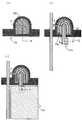
도 1a에 도시하는 바와 같이, 기판(40) 위에 피막(41)을 형성하고, 피막(41) 위에 반도체막(42)을 형성한다.1A, a
기판(40)은 바륨 보로실리케이트 유리, 알루미노 보로실리케이트 유리, 혹은 알루미노 실리케이트 유리 등, 용융법(fusion method)이나 부유법(floating method)에 의하여 제작되는 무알칼리 유리 기판, 세라믹스 기판 외에, 본 제작 공정의 처리 온도에 견딜 수 있는 내열성을 갖는 플라스틱 기판 등을 사용할 수 있다. 또한, 스테인리스 합금 등의 금속 기판의 표면에 절연막을 형성한 기판을 적용하여도 좋다. 기판(40)이 마더(mother) 유리인 경우, 기판의 크기는 제 1 세대(320mm×400mm), 제 2 세대(400mm×500mm), 제 3 세대(550mm×650mm), 제 4 세대(680mm×880mm 혹은 730mm×920mm), 제 5 세대(1000mm×1200mm 혹은 1100mm×1250mm), 제 6 세대(1500mm×1800mm), 제 7 세대(1900mm×2200mm), 제 8 세대(2160mm×2460mm), 제 9 세대(2400mm×2800mm, 2450mm×3050mm), 제 10 세대(2950mm×3400mm) 등을 사용할 수 있다.The
피막(41)은 CVD법, 스퍼터링법, 인쇄법, 도포법 등을 사용하여 적절히 막을 형성할 수 있다. 피막으로서는 절연막, 도전막 등을 적절히 형성할 수 있다. 절연막의 일례로서는, 산화실리콘막, 질화실리콘막, 산질화실리콘막, 질산화실리콘막 등이 있지만, 이것에 한정되지 않는다. 여기서는, 피막(41)으로서 플라즈마 CVD법 에 의하여 두께 50nm 내지 200nm의 질산화실리콘막을 형성한다.The film (41) can be suitably formed by a CVD method, a sputtering method, a printing method, a coating method, or the like. As the film, an insulating film, a conductive film, or the like can be suitably formed. Examples of the insulating film include a silicon oxide film, a silicon nitride film, a silicon oxynitride film, a silicon oxynitride film, and the like, but the present invention is not limited thereto. Here, as the
여기서 기재하는 산질화실리콘막이란, 그 조성으로서 질소보다 산소의 함유량이 많은 것이고, 조성 범위로서 산소가 55at.% 내지 65at.%, 질소가 1at.% 내지 20 at.%, Si가 25at.% 내지 35at.%, 수소가 0.1at.% 내지 10at.%의 범위로 함유되는 것을 의미한다. 또한, 질산화실리콘막이란 그 조성으로서 산소보다 질소의 함유량이 많은 것이고, 조성 범위로서 산소가 15at.% 내지 30at.%, 질소가 20at.% 내지 35 at.%, Si가 25at.% 내지 35at.%, 수소가 15at.% 내지 25at.%의 범위로 함유되는 것을 의미한다.The silicon oxynitride film described here is a silicon nitride film having a larger content of oxygen than that of nitrogen and having a composition range of 55 at.% To 65 at.% Oxygen, 1 at.% To 20 at.% Of nitrogen, 25 at. To 35 at.%, And hydrogen at a rate of 0.1 at.% To 10 at.%. The silicon oxynitride film has a nitrogen content higher than that of oxygen and has a composition range of 15 at.% To 30 at.% Oxygen, 20 at.% To 35 at.% Nitrogen, and 25 at. %, And hydrogen is contained in the range of 15 at.% To 25 at.%.
반도체막(42)은 실리콘, 게르마늄 등을 포함하는 비정질 반도체막 혹은 미결정 반도체막을 형성한다. 미결정 반도체막으로서는 결정 입경이 0.5nm 내지 100nm, 바람직하게는 1nm 내지 20nm의 미결정 반도체막을 사용할 수 있다. 또한, 반도체막(42)이 미결정 반도체막인 경우, 미결정 반도체막에 비정질 반도체 성분이 포함되어도 좋다. 반도체막(42)의 막 두께는 1nm 내지 100nm, 바람직하게는 2nm 내지 20nm, 바람직하게는 5nm 내지 10nm로 한다.The
여기서 기재하는 미결정 반도체막이란, 비정질과 결정 구조(단결정, 다결정을 포함함)의 중간적인 구조의 반도체를 포함하는 막이다. 이 반도체는 자유 에너지적으로 안정된 제 3 상태를 갖는 반도체로서, 단거리 질서를 갖고 격자 왜곡을 갖는 결정질의 것이고, 입자 직경이 0.5nm 내지 100nm, 바람직하게는 1nm 내지 20nm의 기둥 형상 혹은 침상(針狀)의 결정이 기판 표면에 대하여 법선(normal) 방향으로 성장한다. 또한, 복수의 미결정 반도체 사이에 비단결정 반도체가 존재한 다. 미결정 반도체의 대표적인 예인 미결정 실리콘은 그 라만 스펙트럼이 단결정 실리콘을 나타내는 520cm-1보다도 저파수(低波數) 측으로 시프트(shift)한다. 즉, 단결정 실리콘을 나타내는 520cm-11와 비정질 실리콘을 나타내는 480cm-1 사이에 미결정 실리콘의 라만 스펙트럼의 피크가 있다. 또한, 미결합수(未結合手)(댕글링 본드(dangling bond))를 종단하기 위하여 수소 혹은 할로겐을 적어도 1at.% 혹은 그 이상 함유시킨다. 또한, 헬륨, 아르곤, 크립톤, 네온 등의 희소 가스 원소를 함유시켜 격자 왜곡을 더욱 촉진함으로써, 안정성이 높아지고 양호한 미결정 반도체막을 얻을 수 있다. 이러한 미결정 반도체막에 관한 기재는, 예를 들어, 미국 특허 4,409,134호에 개시된다.The microcrystalline semiconductor film described here is a film containing a semiconductor having an intermediate structure of amorphous and crystalline structure (including single crystal and polycrystal). This semiconductor is a semiconductor having a third state that is stable in free energy, and is a crystalline material having a short-range order and having a lattice distortion. The semiconductor is a columnar or acicular shape having a particle diameter of 0.5 nm to 100 nm, preferably 1 nm to 20 nm ) Grows in the normal direction with respect to the substrate surface. In addition, a non-single crystal semiconductor exists between a plurality of microcrystalline semiconductors. The microcrystalline silicon, which is a typical example of the microcrystalline semiconductor, shifts its Raman spectrum to a lower wave number side than 520 cm-1 representing single crystal silicon. In other words, the peak of the Raman spectrum of the microcrystalline silicon between 480cm-1 to
반도체막(42)은 스퍼터링법이나 CVD법에 의하여 형성할 수 있다. 반도체막(42)을 스퍼터링법으로 형성하는 경우, 수소, 혹은 희소 가스를 사용하여 실리콘 타깃을 스퍼터링하여, 상기 피막 위에 상기 반도체막으로서 비정질 반도체막을 형성한다. 반도체막(42)을 CVD법에 의하여 형성하는 경우, 실리콘 혹은 게르마늄을 함유하는 퇴적성 기체와 함께 수소를 플라즈마 CVD 장치의 반응실에 도입하고, 고주파 전력을 인가하여 플라즈마를 발생시킴으로써, 피막 위에 반도체막(42)으로서 비정질 반도체막 혹은 미결정 반도체막을 형성한다.The
실리콘, 혹은 게르마늄을 함유하는 퇴적성 기체로서는 SiH4, Si2H6, GeH4, Ge2H6 등이 있다.As the deposition sex gas containing silicon, germanium or the likeSiH 4, Si 2 H 6, GeH 4, Ge 2 H 6.
또한, 반도체막으로서 비정질 반도체막을 형성하는 일 형태로서, 반응실에 있어서, 실리콘 혹은 게르마늄을 함유하는 퇴적성 기체를 사용한 글로우 방전 플라즈마에 의하여 비정질 반도체막을 형성할 수 있다. 또한, 실리콘, 혹은 게르마늄을 함유하는 퇴적성 기체에 헬륨, 아르곤, 크립톤, 네온 중에서 선택된 1종 혹은 복수종의 희소 가스 원소로 희석하여 글로우 방전 플라즈마에 의하여 비정질 반도체막을 형성할 수도 있다. 또한, 실란 가스의 유량의 1배 이상 10배 이하, 더 바람직하게는 1배 이상 5배 이하의 유량의 수소를 사용한 글로우 방전 플라즈마에 의하여 비정질 반도체막을 형성할 수 있다.As a form of forming an amorphous semiconductor film as a semiconductor film, an amorphous semiconductor film can be formed in a reaction chamber by a glow discharge plasma using a deposition gas containing silicon or germanium. Further, an amorphous semiconductor film may be formed by a glow discharge plasma by diluting the deposition gas containing silicon or germanium with one or more rare gas elements selected from helium, argon, krypton, and neon. Further, the amorphous semiconductor film can be formed by glow discharge plasma using hydrogen at a flow rate of 1 to 10 times, more preferably 1 to 5 times the flow rate of the silane gas.
또한, 반도체막으로서 미결정 반도체막을 형성하는 일 형태로서, 반응실 내에 있어서, 실리콘 혹은 게르마늄을 함유하는 퇴적성 기체, 여기서는 실란과, 수소 및/혹은 희소 가스를 혼합하여 글로우 방전 플라즈마에 의하여 미결정 반도체막을 형성한다. 실란은 수소 및/혹은 희소 가스로 10배 내지 2000배로 희석된다. 따라서, 다량의 수소 및/혹은 희소 가스가 필요하다. 기판의 가열 온도는 100℃ 내지 300℃, 바람직하게는 120℃ 내지 220℃로 행한다. 미결정 반도체막의 성장 표면을 수소로 불활성화하고, 미결정 실리콘의 성장을 촉진하기 위하여는, 120℃ 내지 220℃로 성막을 행하는 것이 바람직하다.As a form of forming a microcrystalline semiconductor film as a semiconductor film, a deposition gas containing silicon or germanium, here, silane, hydrogen and / or a rare gas is mixed in the reaction chamber and glow discharge plasma is used to mix the microcrystalline semiconductor film . The silane is diluted 10 to 2000 times with hydrogen and / or rare gas. Therefore, a large amount of hydrogen and / or rare gas is required. The heating temperature of the substrate is 100 占 폚 to 300 占 폚, preferably 120 占 폚 to 220 占 폚. In order to inactivate the growth surface of the microcrystalline semiconductor film with hydrogen and promote the growth of the microcrystalline silicon, it is preferable to perform the film formation at 120 ° C to 220 ° C.
반도체막(42) 형성 공정에 있어서, 글로우 방전 플라즈마는 1MHz 내지 20MHz, 대표적으로는, 13.56MHz의 고주파 전력, 혹은 20MHz보다 크고 120MHz 정도까지의 VHF 대역의 고주파 전력, 대표적으로는, 27.12MHz 혹은 60MHz를 인가함으로써 생성된다.In the process of forming the
다음에, 결정성이 높은 결정핵을 밀도 높게 형성하는 공정을 행한다. 여기서는, 플라즈마 CVD 장치의 반응실 내에 불소, 플루오르화물 기체, 혹은 수소의 적어도 하나 이상을 도입하고 고주파 전원을 인가하여 플라즈마(43)를 발생시키고, 도 1b에 도시하는 바와 같이, 상기 플라즈마(43)를 반도체막(42)에 노출함으로써, 반도체막(42)의 일부분, 대표적으로는 비정질 반도체 성분을 에칭한다.Next, a step of forming a crystal nucleus having a high crystallinity at a high density is performed. Here, at least one or more of fluorine, fluoride gas, or hydrogen is introduced into the reaction chamber of the plasma CVD apparatus and a high frequency power source is applied to generate the
불소, 플루오르화물 기체, 수소 중의 적어도 하나 이상을 도입하고 고주파 전원을 인가함으로써, 수소 플라즈마, 불소 플라즈마가 발생된다. 수소 플라즈마는 반응실 내에 수소를 도입하여 플라즈마를 발생시킨다. 불소 플라즈마는 반응실 내에 불소 혹은 플루오르화물을 도입하여 플라즈마를 발생시킨다. 플루오르화물 가스로서는 HF, SiF4, SiHF3, SiH2F2, SiH3F, Si2F6, GeF4, GeHF3, GeH2F2, GeH3F, Ge2F6 등이 있다. 또한, 불소, 플루오르화물 기체, 수소 외에 희소 가스를 반응실 내에 도입하여 희소 가스 플라즈마를 발생시켜도 좋다.At least one of fluorine, fluoride gas, and hydrogen is introduced and a high frequency power source is applied to generate a hydrogen plasma and a fluorine plasma. The hydrogen plasma generates hydrogen by introducing hydrogen into the reaction chamber. Fluorine plasma introduces fluorine or fluoride into the reaction chamber to generate plasma. Examples of the fluoride gas include HF, SiF4 , SiHF3 , SiH2 F2 , SiH3 F, Si2 F6 , GeF4 , GeHF3 , GeH2 F2 , GeH3 F and Ge2 F6 . Further, a rare gas plasma may be generated by introducing a rare gas other than fluorine, fluoride gas, and hydrogen into the reaction chamber.
수소 플라즈마, 불소 플라즈마 등에 의하여, 수소 라디칼, 불소 라디칼이 플라즈마 중에 생성된다. 수소 라디칼은 비정질 반도체막과 반응하여 비정질 반도체막을 부분적으로 결정화시킴과 함께, 비정질 반도체 성분을 에칭한다. 불소 라디칼은 반도체막의 비정질 반도체 성분을 에칭한다. 따라서, 반도체막(42)이 미결정 반도체막인 경우, 막에 함유되는 결정립은 작기 때문에, 그 사이를 충전하는 비정질 반도체 성분을 에칭함으로써, 결정성이 높은 결정핵을 밀도 높게 잔존시킬 수 있다. 또한, 피막 위에 형성되는 반도체막이 비정질 반도체막인 경우는, 비정질 반도체 성분을 에칭함과 함께, 부분적으로 결정화하여 미세한 결정핵을 밀도 높게 형성할 수 있다. 따라서, 피막과의 계면에 있어서의 비정질 반도체 성분도 플라즈마에 의하여 에칭되기 때문에, 피막 위에는 결정성이 높은 결정핵을 밀도 높게 형성할 수 있다.Hydrogen plasma, fluorine plasma, etc., hydrogen radicals and fluorine radicals are generated in the plasma. The hydrogen radical reacts with the amorphous semiconductor film to partially crystallize the amorphous semiconductor film and etch the amorphous semiconductor component. The fluorine radicals etch the amorphous semiconductor component of the semiconductor film. Therefore, when the
이 때, 결정핵의 크기를 5nm 내지 30nm, 밀도를 1×10¹⁰atoms/cm3 내지 1×10¹²atoms/cm3로 하면, 미세한 결정핵을 밀도 높게 형성할 수 있고, 이후 형성하는 미결정 반도체막의 결정 밀도를 높일 수 있다.At this time, when the size of the crystal nucleus is 5 nm to 30 nm and the density is 1 × 10¹⁰ atoms / cm3 to 1 × 10¹² atoms / cm3 , fine crystal nuclei can be formed with high density, The crystal density of the film can be increased.
플라즈마의 발생 방법은 HF대역(3MHz 내지 30MHz, 대표적으로는 13.56MHz)을 사용하는 것이 바람직하다. 특히, 13.56MHz의 고주파 전력을 사용함으로써, 플라즈마의 균일성을 높일 수 있고, 제 6 세대 내지 제 10 세대의 대면적 기판 위에 있어서도 균일성이 높은 플라즈마를 반도체막에 노출할 수 있기 때문에 대량 생산에 적합하다.It is preferable to use the HF band (3 MHz to 30 MHz, typically 13.56 MHz) as the generation method of the plasma. Particularly, by using high frequency power of 13.56 MHz, uniformity of the plasma can be enhanced, and plasma having a high uniformity even on the sixth to tenth generation large area substrates can be exposed to the semiconductor film, Suitable.
다음에, 실리콘 혹은 게르마늄을 함유하는 퇴적성 기체, 불소 혹은 플루오르화물 기체, 및 수소를 사용하여 결정핵(44)으로부터 결정 성장시킴으로써, 도 1d에 도시하는 바와 같이, 미결정 반도체막(45)을 형성한다. 플루오르화물 가스로서는 HF, SiF4, SiHF3, SiH2F2, SiH3F, Si2F6, GeF4, GeHF3, GeH2F2, GeH3F, Ge2F6 등이 있다. 여기서는 실란, 불화실란, 수소 및/혹은 희소 가스를 혼합하여, 글로우 방전 플라즈마에 의하여 미결정 반도체막(45)을 형성한다.Next, as shown in Fig. 1D, a
미결정 반도체막을 형성하기 위하여, 실리콘 혹은 게르마늄을 함유하는 퇴적 성 기체와 함께 실리콘 혹은 게르마늄을 함유하는 플루오르화물 가스를 사용함으로써, 결정핵으로부터 결정 성장할 때, 결정 성장이 일어나는 곳의 비정질 반도체 성분을 불소 라디칼이 에칭하기 때문에, 결정성이 높은 결정 성장이 일어난다. 즉, 결정성이 높은 결정립을 형성할 수 있다. 또한, 결정핵의 밀도가 높으면, 인접하는 결정핵의 거리가 짧고 결정 성장할 때에 결정립이 연결된다. 그 후, 결정 성장은 피막 표면에 대하여 법선 방향으로 결정 성장하기 때문에, 기둥 형상의 결정립이 밀접하게 연결된 미결정 반도체막을 형성할 수 있다. 또한, 피막(41) 위에 있는 결정핵으로부터 결정 성장하기 때문에, 피막과의 계면에 있어서의 결정성이 높고 또 막 중의 결정성도 높은 미결정 반도체막을 형성할 수 있다. 또한, 이러한 미결정 반도체막을 박막 트랜지스터의 채널 형성 영역에 사용함으로써, 결정성이 높은 미결정 반도체막을 채널 형성 영역에 갖는 박막 트랜지스터를 제작할 수 있다.A fluoride gas containing silicon or germanium is used together with a deposition gas containing silicon or germanium to form a microcrystalline semiconductor film. When a crystal is grown from a crystal nucleus, an amorphous semiconductor component where crystal growth occurs is referred to as a fluorine radical Etching is performed, so that crystal growth with high crystallinity occurs. That is, a crystal grain with high crystallinity can be formed. When the density of the crystal nuclei is high, the distance between the adjacent crystal nuclei is short and the crystal grains are connected when the crystal is grown. Thereafter, the crystal growth grows in the normal direction with respect to the film surface, so that the microcrystalline semiconductor film in which the columnar crystal grains are closely connected can be formed. In addition, since the crystal is grown from the crystal nuclei on the
또한, 미결정 반도체막의 형성 공정에 있어서, 글로우 방전 플라즈마는 1MHz 내지 20MHz, 대표적으로는, 13.56MHz의 고주파 전력, 혹은 20MHz보다 크고 120MHz 정도까지의 VHF 대역의 고주파 전력, 대표적으로는, 27.12MHz, 60MHz를 인가함으로써 생성된다.In the process of forming the microcrystalline semiconductor film, the glow discharge plasma has a high frequency power of 1 MHz to 20 MHz, typically 13.56 MHz, or a high frequency power of more than 20 MHz and a VHF band of about 120 MHz, typically 27.12 MHz, Lt; / RTI >
또한, 반도체막(42)을 형성하기 전에, 성막 장치의 반응실 내벽에 비정질 반도체막 혹은 미결정 반도체막을 형성하는 것이 바람직하다. 또한, 반응실 내벽을 불소 플라즈마 등으로 클리닝한 후, 반응실 내벽에 비정질 반도체막 혹은 미결정 반도체막을 형성하는 것이 바람직하다. 이러한 처리에 의하여, 반도체막(42) 혹은 미결정 반도체막(45)을 형성할 때, 반응실의 내벽의 성분이나 클리닝에 사용한 불소가, 반도체막(42) 혹은 미결정 반도체막(45) 중에 혼입되는 것을 저감할 수 있다.Before the
상술한 공정에 의하여, 피막과의 계면에 있어서의 결정성이 높고 또 막 중의 결정성도 높은 미결정 반도체막을 형성할 수 있다.By the above-described process, a microcrystalline semiconductor film having high crystallinity at the interface with the film and high crystallinity in the film can be formed.
(실시형태 2)(Embodiment 2)
본 실시형태에서는, 실시형태 1과 마찬가지로 피막과의 계면에 있어서의 결정성이 높고 또 막 중의 결정성도 높은 미결정 반도체막을 형성하는 공정에 대하여 도 2a 내지 도 2d를 사용하여 설명한다.In this embodiment, a step of forming a microcrystalline semiconductor film having a high crystallinity at the interface with the film and a high crystallinity in the film as in
도 2a에 도시하는 바와 같이, 기판(40) 위에 피막(41)을 형성한다.As shown in Fig. 2A, a
다음에, 피막(41) 표면을 플라즈마(46)에 노출하여 표면에 요철을 갖는 피막(41a)을 형성한다. 요철의 형상으로서는 도 2b에 도시하는 바와 같이, 볼록부 및 오목부가 각각 완만한 곡선 형상인 파상 형상이라도 좋다. 또한, 볼록부의 선단은 침 형상으로 뾰족하고 오목부는 완만한 곡선 형상으로 할 수도 있다. 또한, 요철의 간격은 좁으면, 이후에 밀도가 높은 결정핵을 형성할 수 있으므로, 바람직하다.Next, the surface of the
플라즈마(46)로서 피막(41)의 표면에 요철을 생기게 하는 플라즈마(46)를 피막(41)에 노출한다. 이러한 플라즈마로서는 반응실 내에 불소, 플루오르화물 기체, 수소 중의 적어도 하나 이상을 도입하고 고주파 전원을 인가하여 플라즈마(46)를 발생시키고, 상기 플라즈마(46)를 피막(41)에 노출함으로써 피막(41)의 표면을 에칭하여 요철을 갖는 피막(41a)으로 한다.As the
다음에, 피막(41a) 위에 반도체막(42)을 형성한다. 반도체막(42)은 피막(41a) 표면의 요철의 영향을 받아, 반도체막(42) 표면도 요철을 가진다. 다음에, 실시형태 1과 마찬가지로, 결정성이 높은 결정핵을 밀도 높게 형성하는 공정을 행한다. 여기서도 마찬가지로, 플라즈마 CVD 장치의 반응실 내에, 불소, 플루오르화물 기체, 수소 중의 적어도 하나 이상을 도입하여 고주파 전원을 인가하여 플라즈마(43)를 발생시키고, 상기 플라즈마(43)를 반도체(42)에 노출함으로써, 반도체막(42)의 일부분, 대표적으로는 비정질 반도체 성분을 에칭한다. 또한, 본 실시형태에서는, 반도체막(42)의 표면이 요철을 가지므로, 반도체막(42)의 응력 집중(stress concentration)에 의하여 결정핵이 형성되기 쉽게 된다. 또한, 반도체막(42)의 Si의 결합수가 (110)면 외의 면에서도 결합하므로, 결합이 더 강고하게 되고, 피막과 결정핵, 또 게이트 절연막과 미결정 반도체막의 밀착성이 향상된다.Next, the
결과적으로, 도 2c에 도시하는 바와 같은, 결정성이 높은 결정핵(44)을 형성할 수 있다.As a result, a
다음에, 실리콘 혹은 게르마늄을 함유하는 퇴적성 기체, 불소 혹은 플루오르화물 기체, 및 수소를 반응실 내에 도입하고, 고주파 전원을 인가하여 결정핵(44)으로부터 결정 성장시킴으로써, 도 2d에 도시하는 바와 같이, 미결정 반도체막(45)을 형성한다. 플루오르화물 가스로서는 HF, SiF4, SiHF3, SiH2F2, SiH3F, Si2F6, GeF4, GeHF3, GeH2F2, GeH3F, Ge2F6 등이 있다. 여기서는 실란, 불화실란, 수소 및/ 혹은 희소 가스를 혼합하여, 글로우 방전 플라즈마에 의하여 미결정 반도체막을 형성한다.Next, a deposition gas containing silicon or germanium, a fluorine or fluoride gas, and hydrogen are introduced into the reaction chamber and a high frequency power source is applied to grow crystal from the
또한, 반도체막(42)을 형성하기 전에, 성막 장치의 반응실 내벽에 비정질 반도체막 혹은 미결정 반도체막을 형성하는 것이 바람직하다. 또한, 반응실 내벽을 불소 플라즈마 등으로 클리닝한 후, 반응실 내벽에 비정질 반도체막 혹은 미결정 반도체막을 형성하는 것이 바람직하다. 이러한 처리에 의하여, 반도체막(42) 혹은 미결정 반도체막(45)을 형성할 때, 반응실 내벽의 성분이나 클리닝에 사용한 불소가 반도체막(42) 혹은 미결정 반도체막(45) 중에 혼입되는 것을 저감할 수 있다.Before the
상술한 공정에 의하여, 피막과의 계면에 있어서의 결정성이 높고, 또 막 중의 결정성도 높은 미결정 반도체막을 형성할 수 있다.By the above-described process, a microcrystalline semiconductor film having high crystallinity at the interface with the coating film and high crystallinity in the film can be formed.
(실시형태 3)(Embodiment 3)
본 실시형태에서는 피막과의 계면의 결정성이 높고, 또 인접하는 결정립의 밀착성이 높은 미결정 반도체막, 즉, 결함이 적은 미결정 반도체막의 제작 공정에 대하여, 도 3a 내지 도 3d를 사용하여 설명한다.In this embodiment mode, a process for manufacturing a microcrystalline semiconductor film having high crystallinity at the interface with the coating film and high adhesion of adjacent crystal grains, that is, a microcrystalline semiconductor film with few defects will be described with reference to FIGS. 3A to 3D.
도 3a에 도시하는 바와 같이, 기판(40) 위에 피막(41)을 형성하고, 피막(41) 위에 반도체막(47)을 형성한다.3A, a
여기서는, 반도체막(47)으로서, 도너로서 기능하는 불순물 원소를 함유하는 반도체막을 형성한다. 도너로서 기능하는 불순물 원소를 함유하는 반도체막을 플라즈마 CVD법 혹은 스퍼터링법에 의하여 형성한다. 도너로서 기능하는 불순물 원소에는, 도너 원소로서 인, 비소, 혹은 안티몬을 사용한다. 또한, 반도체막으로서 는, 비정질 반도체막 혹은 미결정 반도체막을 형성한다. 또한, 비정질 반도체막 혹은 미결정 반도체막으로서는, 실리콘 혹은 게르마늄을 함유하는 비정질 반도체 혹은 미결정 반도체막을 형성한다.Here, as the
도너로서 기능하는 불순물 원소를 함유하는 반도체막의 형성 방법으로서는, 반도체막의 원료 기체와 함께, 도너로서 기능하는 불순물 원소를 함유하는 기체를 사용하여 반도체막을 형성하면 좋다. 예를 들어, 실란 및 수소와 함께, 포스핀을 사용한 플라즈마 CVD법에 의하여 인을 포함하는 비정질 실리콘막 혹은 미결정 실리콘막을 형성할 수 있다.As a method of forming a semiconductor film containing an impurity element serving as a donor, a semiconductor film may be formed by using a substrate containing an impurity element which functions as a donor together with a source gas of a semiconductor film. For example, an amorphous silicon film or a microcrystalline silicon film containing phosphorus can be formed by a plasma CVD method using a phosphine together with silane and hydrogen.
도너로서 기능하는 불순물 원소의 농도는, 6×10¹⁵atoms/cm3 이상 3×10¹⁸atoms/cm3 이하, 바람직하게는 1×10¹⁶atoms/cm3 이상 3×10¹⁸atoms/cm3 이하, 바람직하게는 3×10¹⁶atoms/cm3 이상 3×10¹⁷atoms/cm3 이하다. 도너로서 기능하는 불순물 원소의 농도를 상기 범위 내로 함으로써, 피막(41), 및 이후 형성되는 도너로서 기능하는 불순물 원소를 함유하는 미결정 반도체막의 계면의 결정성을 높일 수 있다. 또한, 이후 형성되는 도너로서 기능하는 불순물 원소를 함유하는 미결정 반도체막의 저항률을 저감할 수 있다.The concentration of the impurity element serving as a donor is 6 x 10¹⁵ atoms / cm3 to 3 x 10¹⁸ atoms / cm3 , preferably 1 x 10¹⁶ atoms / cm3 to 3 x 10¹⁸ atoms / cm3 , Preferably not less than 3 x 10¹⁶ atoms / cm3 and not more than 3 x 10¹⁷ atoms / cm3 . By setting the concentration of the impurity element functioning as a donor within the above range, the crystallinity of the interface of the
또한, 반도체막(47)을 형성하기 전에, 성막 장치의 반응실 내에 도너로서 기능하는 불순물 원소를 함유하는 기체를 흘리고, 피막(41) 표면 및 반응실 내벽에 도너로서 기능하는 불순물 원소를 흡착시켜도 좋다. 그 후, 반도체막(47)을 형성함으로써, 도너로서 기능하는 불순물 원소를 흡수하면서 반도체막이 퇴적되기 때문 에, 도너로서 기능하는 불순물 원소를 함유하는 반도체막(47)을 형성할 수 있다.Before the
다음에, 반도체막(47)을 사용하여 결정성이 높은 결정핵을 밀도 높게 형성하는 공정을 행한다. 여기서는, 도 3b에 도시하는 바와 같이, 반도체막(47)에 플라즈마(43)를 조사한다. 이 결과, 도 3c에 도시하는 바와 같이, 피막(41) 위에 도너로서 기능하는 불순물 원소를 함유하는 결정핵(48)을 형성한다. 플라즈마(43)로서는, 실시형태 1에 제시하는 플라즈마(43)를 적절히 사용할 수 있다.Next, a step of forming a crystal nucleus having a high crystallinity at a high density by using the
또한, 플라즈마(43)는 반응실에 수소, 불소, 혹은 플루오르화물과 함께, 도너로서 기능하는 불순물 원소를 함유하는 기체를 도입하여 발생시킨 플라즈마라도 좋다. 수소, 불소, 혹은 플루오르화물로 반도체막(47)의 비정질 반도체 성분을 에칭함과 함께, 도너로서 기능하는 불순물 원소를 잔존하는 반도체막에 첨가함으로써, 도너로서 기능하는 불순물 원소를 함유하는 결정핵(48)을 형성할 수 있다.The
다음에, 실리콘 혹은 게르마늄을 함유하는 퇴적성 기체, 실리콘 혹은 게르마늄을 함유하는 플루오르화물 가스, 및 수소를 반응실 내에 도입하여 고주파 전원을 인가하여 결정핵(48)으로부터 결정 성장시킴으로써, 도 3d에 도시하는 바와 같이, 도너로서 기능하는 불순물 원소를 포함하는 미결정 반도체막(49)을 형성한다. 실리콘 혹은 게르마늄을 함유하는 퇴적성 기체로서는, SiH4, Si2H6, GeH4, Ge2H6 등이 있다. 실리콘 혹은 게르마늄을 함유하는 플루오르화물 가스로서는, HF, SiF4, SiHF3, SiH2F2, SiH3F, Si2F6, GeF4, GeHF3, GeH2F2, GeH3F, Ge2F6 등이 있다. 여기서는 실란, 불화실란, 수소 및/혹은 희소 가스를 혼합하여 글로우 방전 플라즈마에 의하여 도너로서 기능하는 불순물 원소를 함유하는 미결정 반도체막을 형성한다.Next, by introducing a deposition gas containing silicon or germanium, a fluoride gas containing silicon or germanium, and hydrogen into the reaction chamber and applying a high frequency power source to grow crystals from the
미결정 반도체막을 형성하기 위하여, 실리콘 혹은 게르마늄을 함유하는 퇴적성 기체와 함께, 실리콘 혹은 게르마늄을 함유하는 플루오르화물 가스를 사용함으로써, 결정핵으로부터 결정 성장할 때, 결정 성장이 일어나는 곳의 비정질 반도체 성분을 불소 라디칼이 에칭되기 때문에, 결정성이 높은 결정 성장이 일어난다. 즉, 결정성이 높은 결정립을 형성할 수 있다. 또한, 결정핵의 밀도가 높으면, 인접하는 결정핵의 거리가 짧고 결정 성장할 때에 결정립이 연결된다. 그 후, 결정 성장은 피막 표면에 대하여 법선 방향으로 결정 성장하기 때문에, 기둥 형상의 결정립이 밀접하게 연결된 미결정 반도체막을 형성할 수 있다. 또한, 피막 위에 있는 결정핵으로부터 결정 성장하기 때문에, 피막과의 계면의 결정성이 높고 또 막 중의 결정성도 높은 미결정 반도체막을 형성할 수 있다. 또한, 이러한 미결정 반도체막에 도너로서 기능하는 불순물 원소가 함유되기 때문에 미결정 반도체막의 저항률을 저감할 수 있다.In order to form a microcrystalline semiconductor film, a fluoride gas containing silicon or germanium is used together with a deposition gas containing silicon or germanium. When the crystal is grown from crystal nuclei, the amorphous semiconductor component where crystal growth occurs is referred to as fluorine radical Is etched, crystal growth with high crystallinity occurs. That is, a crystal grain with high crystallinity can be formed. When the density of the crystal nuclei is high, the distance between the adjacent crystal nuclei is short and the crystal grains are connected when the crystal is grown. Thereafter, the crystal growth grows in the normal direction with respect to the film surface, so that the microcrystalline semiconductor film in which the columnar crystal grains are closely connected can be formed. In addition, since the crystal is grown from the crystal nuclei on the coating film, the microcrystalline semiconductor film having a high crystallinity at the interface with the coating film and high crystallinity in the film can be formed. In addition, since the impurity element serving as a donor is contained in the microcrystalline semiconductor film, the resistivity of the microcrystalline semiconductor film can be reduced.
또한, 반도체막(47)을 형성하기 전에, 성막 장치의 반응실 내벽에 비정질 반도체막 혹은 미결정 반도체막을 형성하는 것이 바람직하다. 또한, 반응실 내벽을 불소 플라즈마 등으로 클리닝한 후, 반응실 내벽에 비정질 반도체막 혹은 미결정 반도체막을 형성하는 것이 바람직하다. 이러한 처리에 의하여, 반도체막(47)을 형성할 때, 반응실 내벽의 성분이나 클리닝에 사용한 불소가, 반도체막(47) 중에 혼입되는 것을 저감할 수 있다. 또한, 반응실 내벽에 형성하는 비정질 반도체막 혹은 미결정 반도체막에 도너로서 기능하는 불순물 원소를 첨가하여도 좋다. 도너로 서 기능하는 불순물 원소의 농도는, 6×10¹⁵atoms/cm3 이상 3×10¹⁸atoms/cm3 이하, 바람직하게는 1×10¹⁶atoms/cm3 이상 3×10¹⁸atoms/cm3 이하, 바람직하게는 3×10¹⁶atoms/cm3 이상 3×10¹⁷atoms/cm3 이하다. 이러한 처리에 의하여, 반응실 내의 압력을 진공 배기할 때, 반응실 내벽에 부착하는 도너로서 기능하는 불순물 원소가 반응실 내에 해리된다. 상기 해리된 도너로서 기능하는 불순물 원소는 반도체막(47)에 혼입되기 때문에, 도너로서 기능하는 불순물 원소를 함유하는 반도체막(47)을 형성할 수 있다.Before the
또한, 도너로서 기능하는 불순물 원소를 함유하는 반도체막(47)을 형성하는 대신에, 도너로서 기능하는 불순물 원소를 함유하지 않는 반도체막을 형성하고, 피막(41)에 도너로서 기능하는 불순물을 함유하는 절연막을 형성하여도 좋다. 예를 들어, 도너로서 기능하는 불순물 원소(인, 비소, 혹은 안티몬)를 함유하는 산화실리콘막, 질화실리콘막, 산질화실리콘막, 혹은 질산화실리콘막 등을 사용하여 형성할 수 있다. 또한, 피막(41)을 적층 구조로 하는 경우, 반도체막(47)에 접하는 층 혹은 기판(40)에 접하는 층에 도너로서 기능하는 불순물 원소를 첨가하여도 좋다.Instead of forming the
피막(41)으로서 도너로서 기능하는 불순물 원소를 함유하는 절연막을 형성하는 방법으로서는, 절연막의 원료 기체와 함께, 도너로서 기능하는 불순물 원소를 함유하는 기체를 사용하여 절연막을 형성하면 좋다. 예를 들어, 실란, 암모니아, 및 포스핀을 사용한 플라즈마 CVD법에 의하여 인을 함유하는 질화실리콘막을 형성할 수 있다. 또한, 실란, 일산화이질소, 암모니아, 포스핀을 사용한 플라즈마 CVD 법에 의하여, 인을 함유하는 산질화실리콘막을 형성할 수 있다.As a method for forming an insulating film containing an impurity element serving as a donor as the
또한, 피막(41)을 형성하기 전에, 성막 장치의 반응실 내에 도너로서 기능하는 불순물 원소를 함유하는 기체를 흘리고, 기판(40) 표면 및 반응실 내벽에 도너로서 기능하는 불순물 원소를 흡착시켜도 좋다. 그 후, 피막(41)을 형성함으로써, 도너로서 기능하는 불순물 원소를 흡수하면서 반도체막이 퇴적되기 때문에, 도너로서 기능하는 불순물 원소를 함유하는 반도체막(47)을 형성할 수 있다.A gas containing an impurity element functioning as a donor may be flowed into the reaction chamber of the film forming apparatus before the
또한, 미결정 반도체막(49)으로서, 도너로서 기능하는 불순물 원소를 함유하는 미결정 반도체막을 형성하여도 좋다. 도너로서 기능하는 불순물 원소를 함유하는 미결정 반도체막의 형성 방법으로서는, 미결정 반도체막의 원료 기체와 함께, 도너로서 기능하는 불순물 원소를 함유하는 기체를 사용하면 좋다. 예를 들어, 실란, 불화실란, 및 수소, 및 포스핀을 사용한 플라즈마 CVD법에 의하여 인을 함유하는 미결정 실리콘막을 형성할 수 있다.As the
또한, 미결정 반도체막(49)을 형성하기 전에, 성막 장치의 반응실 내에 도너로서 기능하는 불순물 원소를 함유하는 기체를 흘리고, 피막(41) 및 결정핵(48) 표면 및 반응실 내벽에 도너로서 기능하는 불순물 원소를 흡착시켜도 좋다. 그 후, 미결정 반도체막(49)을 퇴적함으로써, 도너로서 기능하는 불순물 원소를 흡수하면서 미결정 반도체막이 퇴적되기 때문에, 도너로서 기능하는 불순물 원소를 함유하는 미결정 반도체막(49)을 형성할 수 있다.Before the formation of the
또한, 피막(41), 반도체막(47), 결정핵(48), 미결정 반도체막(49) 중의 어느 2개 위에 도너로서 기능하는 불순물 원소를 첨가하여도 좋다.An impurity element functioning as a donor may be added to any two of the
상술한 공정에 의하여, 피막과의 계면에 있어서의 결정성이 높고 또 막 중의 결정성도 높고, 저항률이 낮은 미결정 반도체막을 형성할 수 있다.By the above-described process, a microcrystalline semiconductor film having high crystallinity at the interface with the film, high crystallinity in the film, and low resistivity can be formed.
(실시형태 4)(Fourth Embodiment)
본 실시형태에서는 상기 실시형태 1 내지 상기 실시형태 3에 제시하는 미결정 반도체막을 사용한 박막 트랜지스터의 제작 공정에 대하여 제시한다. 본 실시형태에서는 미결정 반도체막의 제작 방법으로서 실시형태 1을 사용하여 제시하지만, 실시형태 2 및 실시형태 3을 적절히 적용할 수 있다.In this embodiment mode, a manufacturing process of a thin film transistor using the microcrystalline semiconductor film described in any of the first to third embodiments is described. In the present embodiment, the method of manufacturing the microcrystalline semiconductor film is described using
미결정 반도체막을 갖는 박막 트랜지스터는, p형 박막 트랜지스터보다 n형 박막 트랜지스터가 이동도가 높기 때문에 구동회로에 사용하는 데에 더 적합하다. 동일 기판 위에 형성하는 박막 트랜지스터를 모두 동일 극성으로 일치시키는 것이 공정수를 억제하기 위해서도 바람직하다. 여기서는, n채널형 박막 트랜지스터를 사용하여 설명한다.The thin film transistor having the microcrystalline semiconductor film is more suitable for use in the driving circuit because the n-type thin film transistor has higher mobility than the p-type thin film transistor. It is also preferable to make all the thin film transistors formed on the same substrate coincide with the same polarity in order to suppress the number of processes. Here, an n-channel type thin film transistor will be described.
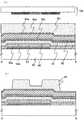
도 4a에 도시하는 바와 같이, 기판(50) 위에 게이트 전극(51)을 형성하고, 게이트 전극(51) 위에 게이트 절연막(52a, 52b)을 형성한다.A
게이트 전극(51)은 금속 재료로 형성된다. 금속 재료로서는 알루미늄, 크롬, 티타늄, 탄탈, 몰리브덴, 구리 등이 적용된다. 게이트 전극(51)의 바람직한 예는 알루미늄 혹은 알루미늄과 배리어 금속의 적층 구조체에 의하여 형성된다. 배리어 금속으로서는 티타늄, 몰리브덴, 크롬 등의 고융점 금속이 적용된다. 배리어 금속은 알루미늄의 힐록 방지, 산화 방지를 위하여 형성하는 것이 바람직하다.The
게이트 전극(51)은 두께 50nm 이상 300nm 이하로 형성한다. 게이트 전 극(51)의 두께를 50nm 이상 100nm 이하로 함으로써, 이후 형성되는 반도체막의 단절이나 배선의 단선을 방지할 수 있다. 또한, 게이트 전극(51)의 두께를 150nm 이상 300nm 이하로 함으로써, 게이트 전극(51)의 저항률을 저감할 수 있고, 기판의 대면적화가 가능하다.The
또한, 게이트 전극(51) 위에는 반도체막이나 배선 등을 형성하기 때문에, 단절이나 단선을 방지하기 위하여 단부가 테이퍼 형상이 되도록 가공하는 것이 바람직하다. 또한, 도시하지 않지만, 이 공정에 의하여 게이트 전극에 접속되는 배선이나 용량 배선도 동시에 형성할 수 있다.In addition, since a semiconductor film, wiring, or the like is formed on the
게이트 절연막(51)은 스퍼터링법, CVD법, 도금법, 인쇄법, 액적 토출법 등을 사용하여 형성한다. 여기서는, 기판(50) 위에 도전막으로서 몰리브덴막을 스퍼터링법에 의하여 형성하고, 제 1 포토마스크를 사용하여 형성한 레지스트 마스크를 사용하여 기판(50) 위에 형성된 도전막을 에칭하여 게이트 전극(51)을 형성한다.The
게이트 절연막(52a, 52b)은 각각, CVD법이나 스퍼터링법 등을 사용하여 산화실리콘막, 질화실리콘막, 산질화실리콘막, 혹은 질산화실리콘막으로 형성할 수 있다. 게이트 절연막(52a, 52b)은 각각 두께 50nm 내지 150nm의 산화실리콘막, 질화실리콘막, 산질화실리콘막, 혹은 질산화실리콘막으로 형성할 수 있다. 여기서는, 게이트 절연막(52a)으로서 질화실리콘막 혹은 질산화실리콘막을 형성하고, 게이트 절연막(52b)으로서 산화실리콘막 혹은 산질화실리콘막을 형성하여 적층하는 형태를 제시한다. 또한, 게이트 절연막을 2층이 아니라, 산화실리콘막, 질화실리콘막, 산질화실리콘막, 혹은 질산화실리콘막의 단층으로 형성할 수 있다.Each of the
게이트 절연막(52a)을 질화실리콘막, 혹은 질산화실리콘막을 사용하여 형성함으로써, 기판(50)과 게이트 절연막(52a)의 밀착력이 높아지고, 기판(50)으로서 유리 기판을 사용한 경우, 기판(50)으로부터의 불순물이 미결정 반도체막에 확산되는 것을 방지할 수 있고, 또한 게이트 전극(51)의 산화를 방지할 수 있다. 즉, 막이 벗겨지는 것을 방지할 수 있는 것과 함께, 이후 형성되는 박막 트랜지스터의 전기 특성을 향상시킬 수 있다. 또한, 게이트 절연막(52a, 52b)은 각각 두께 50nm 이상이면 게이트 전극(51)의 요철로 인한 피복률의 저감을 완화할 수 있기 때문에 바람직하다.The adhesion between the
다음에, 게이트 절연막(52b) 위에 실리콘, 혹은 게르마늄을 함유하는 퇴적성 기체 및 수소를 사용하여 플라즈마 CVD법에 의하여 반도체막(42)을 형성한다.Next, a
여기서는, 일 형태로서, 플라즈마 CVD 장치의 반응실 내에 있어서, 반도체막(42)으로서 미결정 실리콘막을 형성하는 형태를 제시한다. 실리콘 혹은 게르마늄을 함유하는 퇴적성 기체, 여기서는 실란과 수소 및/혹은 희소 가스를 혼합하여 글로우 방전 플라즈마에 의하여 미결정 반도체막을 형성한다. 실란은 수소 및/혹은 희소 가스에 의하여 10배 내지 2000배로 희석된다. 기판의 가열 온도는 100℃ 내지 300℃, 바람직하게는 120℃ 내지 220℃로 행한다.Here, as a form, a mode in which a microcrystalline silicon film is formed as a
다음에, 도 4b에 도시하는 바와 같이, 플라즈마(43)를 반도체막(42)에 노출하여, 도 4c에 도시하는 바와 같이, 결정핵(44)을 형성한다. 여기서는, 일 형태로서, 플라즈마 CVD장치의 반응실 내에서 수소 및/혹은 희소 가스를 혼합하여 글로우 방전 플라즈마에 의하여 수소 플라즈마를 발생시키고, 반도체막(42)에 수소 플라즈 마를 노출함으로써, 반도체막(42)의 비정질 반도체 성분을 에칭하여 결정핵(44)을 형성한다.Next, as shown in Fig. 4B, the
다음에, 결정핵(44)으로부터 결정 성장시켜 미결정 반도체막(45)을 형성한다. 여기서는 일 형태로서 미결정 실리콘을 형성하는 형태를 제시한다.Next, the
플라즈마 CVD 장치의 반응실 내에 있어서, 실리콘 혹은 게르마늄을 함유하는 퇴적성 기체, 여기서는 실란과, 플루오르화물 기체 혹은 불소, 여기서는 불화실란과, 수소 및/혹은 희소 가스를 혼합하여 글로우 방전 플라즈마에 의하여 미결정 실리콘막을 형성한다. 실란의 유량에 대하여 불화실란의 유량을 0.1배 내지 50배, 바람직하게는 1배 내지 10배로 하고, 실란의 유량에 대하여 수소의 유량을 10배 내지 2000배, 바람직하게는 50배 내지 200배로 희석하여 미결정 실리콘막을 형성한다. 기판의 가열 온도는 100℃ 내지 300℃, 바람직하게는 120℃ 내지 220℃로 행한다.In the reaction chamber of the plasma CVD apparatus, a deposition gas containing silicon or germanium, here, silane, a fluoride gas or fluorine, here fluorine silane, hydrogen and / or a rare gas are mixed and a glow discharge plasma is used to mix the microcrystalline silicon film . The flow rate of hydrogen silane is diluted to 10 to 2,000 times, preferably 50 to 200 times, based on the flow rate of the silane, with the flow rate of the silane fluoride being 0.1 to 50 times, preferably 1 to 10 times, Thereby forming a microcrystalline silicon film. The heating temperature of the substrate is 100 占 폚 to 300 占 폚, preferably 120 占 폚 to 220 占 폚.
미결정 반도체막을 형성하기 위하여, 실리콘 혹은 게르마늄을 함유하는 퇴적성 기체와 함께, 실리콘 혹은 게르마늄을 함유하는 플루오르화물 가스를 사용함으로써, 결정핵으로부터 결정 성장할 때, 결정 성장이 일어나는 곳의 비정질 반도체 성분을 불소 라디칼이 에칭하기 때문에, 결정성이 높은 결정 성장이 일어난다. 즉, 결정성이 높은 결정립을 형성할 수 있다.In order to form a microcrystalline semiconductor film, a fluoride gas containing silicon or germanium is used together with a deposition gas containing silicon or germanium. When the crystal is grown from crystal nuclei, the amorphous semiconductor component where crystal growth occurs is referred to as fluorine radical Is etched, crystal growth with high crystallinity occurs. That is, a crystal grain with high crystallinity can be formed.
또한, 실란 등의 가스 중에 GeH4, GeF4 등의 수소화게르마늄, 불화게르마늄을 혼합하여 에너지 밴드 폭을 0.9eV 내지 1.1eV로 조절하여도 좋다. 실리콘에 게르 마늄을 가하면 박막 트랜지스터의 온도 특성을 변화시킬 수 있다.It is also possible to control the energy band width by mixing germanium hydride, germanium fluoride such as GeH4, GeF4 in the gas, such as silane to 0.9eV to about 1.1eV. Applying germanium to silicon can change the temperature characteristics of the thin film transistor.
미결정 반도체막(45)의 두께는 5nm 이상 200nm 이하, 바람직하게는 5nm 이상 100nm 이하, 바람직하게는 5nm 이상 50nm 이하, 바람직하게는 10nm 이상 25nm 이하로 형성한다. 미결정 반도체막(45)의 두께를 5nm 이상 50nm 이하로 함으로써 완전 공핍형 박막 트랜지스터를 제작할 수 있다.The thickness of the
또한, 미결정 반도체막(45)의 산소 농도 및 질소 농도는 3×10¹⁹atoms/cm3 미만, 더 바람직하게는 3×10¹⁸atoms/cm3 미만, 탄소의 농도를 3×10¹⁸atoms/cm3 이하로 하는 것이 바람직하다. 산소, 질소, 및 탄소가 미결정 반도체막에 혼입되는 농도를 저감함으로써, 미결정 반도체막의 결함의 생성을 억제할 수 있다. 또한, 산소 및 질소가 미결정 반도체막 중에 함유되면 결정화되기 어렵다. 따라서, 미결정 반도체막 중의 산소 농도, 질소 농도가 비교적 낮음으로써, 미결정 반도체막의 결정성을 높일 수 있다. 또한, 미결정 반도체막 중에는, 1×10¹⁷atoms/cm3 내지 1×10²⁰atoms/cm3, 바람직하게는 1×10¹⁹atoms/cm3 미만의 불소를 함유한다.The oxygen concentration and the nitrogen concentration in the
또한, 본 실시형태의 미결정 반도체막에는 박막 트랜지스터의 채널 형성 영역으로서 기능하는 미결정 반도체막에 대하여는, 성막과 동시에 혹은 성막 후에, 억셉터로서 기능하는 불순물 원소를 첨가함으로써, 임계값 제어를 할 수 있게 된다. 억셉터로서 기능하는 불순물 원소는 대표적으로는 붕소이고, B2H6, BF3 등의 불순물 기체를 1ppm 내지 1000ppm, 바람직하게는 1ppm 내지 100ppm의 비율로 실리 콘 혹은 게르마늄을 함유하는 퇴적성 기체에 혼입시키면 좋다. 그리고 붕소의 농도는, 도너로서 기능하는 불순물 원소의 10분의 1 정도, 예를 들어 1×10¹⁴atoms/cm3 내지 6×10¹⁶atoms/cm3로 하면 좋다.Further, in the microcrystalline semiconductor film of the present embodiment, a microcrystalline semiconductor film functioning as a channel forming region of the thin film transistor can be controlled to have a threshold value by adding an impurity element that functions as an acceptor simultaneously with or after film formation do. The impurity element functioning as an acceptor is typically boron, and an impurity gas such as B2 H6 or BF3 is added to the deposition gas containing silicon or germanium at a ratio of 1 ppm to 1000 ppm, preferably 1 ppm to 100 ppm It may be mixed. The concentration of boron may be about one tenth of the impurity element serving as a donor, for example, 1 x 10¹⁴ atoms / cm3 to 6 x 10¹⁶ atoms / cm3 .
종래의 미결정 반도체막의 형성 방법을 사용하면 불순물이나 격자 부정합 등의 요인으로 인하여, 퇴적 초기 단계에서 비정질 반도체층이 형성되어 버린다. 역 스태거형 박막 트랜지스터에 있어서는 게이트 절연막의 근방의 반도체막에서 캐리어가 흐르기 때문에, 계면에 비정질 반도체층이 형성되면 이동도가 저하됨과 함께 전류량이 적게 되므로, 박막 트랜지스터의 전기 특성이 저하한다.When a conventional method of forming a microcrystalline semiconductor film is used, an amorphous semiconductor layer is formed at the initial stage of deposition due to factors such as impurities and lattice mismatch. In the inverse stagger type thin film transistor, the carrier flows in the semiconductor film near the gate insulating film. Therefore, when the amorphous semiconductor layer is formed at the interface, the mobility decreases and the amount of current decreases.
그러나, 결정성이 높은 결정핵을 밀도 높게 형성하고, 실리콘 혹은 게르마늄을 함유하는 퇴적성 기체와, 수소와 함께, 플루오르화물 기체 혹은 불소를 원료 가스로 하여, 결정핵을 사용하여 플라즈마 CVD법으로 미결정 반도체막을 형성하면, 상기 결정핵으로부터 결정 성장되기 때문에, 게이트 절연막과의 계면에 비정질 반도체가 형성되는 것을 저감할 수 있다.However, when a crystal nucleus having a high crystallinity is formed at a high density, a deposition gas containing silicon or germanium, a fluoride gas or fluorine as a raw material gas together with hydrogen, and a microcrystalline semiconductor When a film is formed, since the crystal is grown from the crystal nucleus, formation of an amorphous semiconductor at the interface with the gate insulating film can be reduced.
결과적으로, 본 형태에 제시하는 바와 같이, 미결정 반도체막을 게이트 절연막 위에 형성함으로써, 막의 두께 방향에 있어서의 결정성을 높임과 함께, 게이트 절연막 및 미결정 반도체막 계면의 결정성을 높일 수 있다.As a result, as shown in this embodiment, by forming the microcrystalline semiconductor film on the gate insulating film, the crystallinity in the film thickness direction can be increased and the crystallinity of the interface between the gate insulating film and the microcrystalline semiconductor film can be increased.
다음에, 도 4e에 도시하는 바와 같이, 미결정 반도체막(45) 위에, 버퍼층(54) 및 일 도전형을 부여하는 불순물 원소가 첨가된 반도체막(55)을 형성한다. 다음에, 일 도전형을 부여하는 불순물 원소가 첨가된 반도체막(55) 위에 레지스트 마스크(56)를 형성한다.4E, a
버퍼층(54)으로서는 실리콘, 혹은 게르마늄을 함유하는 퇴적성 기체를 사용한 플라즈마 CVD법에 의하여 비정질 반도체막을 형성할 수 있다. 혹은, 실리콘 혹은 게르마늄을 함유하는 퇴적성 기체에, 헬륨, 아르곤, 크립톤, 네온 중에서 선택된 1종 혹은 복수종의 희소 가스 원소로 희석하여 비정질 반도체막을 형성할 수 있다. 혹은, 실란 가스의 유량의 1배 이상 10배 이하, 더 바람직하게는 1배 이상 5배 이하의 유량의 수소를 사용하여 수소를 함유하는 비정질 반도체막을 형성할 수 있다. 또한, 상기 수소화 반도체막에 불소, 염소, 브롬, 요오드 등의 할로겐을 첨가하여도 좋다.As the
또한, 버퍼층(54)은 타깃으로서 실리콘, 게르마늄 등의 반도체 타깃을 사용하여, 수소 혹은 희소 가스로 스퍼터링하여 비정질 반도체막을 형성할 수 있다.The
버퍼층(54)은 결정립을 함유하지 않는 비정질 반도체막으로 형성하는 것이 바람직하다.The
버퍼층(54)은 이후의 소스 영역 및 드레인 영역의 형성 프로세스에 있어서, 부분적으로 에칭되는 경우가 있지만, 그 때, 버퍼층(54)이 부분적으로 잔존하는 두께로 형성하는 것이 바람직하다. 대표적으로는 30nm 이상 500nm 이하, 바람직하게는 50nm 이상 200nm 이하의 두께로 형성하는 것이 바람직하다. 박막 트랜지스터의 인가 전압이 높은(예를 들어, 15V정도) 표시 장치, 대표적으로는 액정 표시 장치에 있어서, 버퍼층(54)을 두껍게 형성하면 내압이 높아지므로, 박막 트랜지스터에 높은 전압이 인가되어도 박막 트랜지스터가 열화하는 것을 회피할 수 있다.Although the
미결정 반도체막(45) 표면에, 비정질 반도체막, 또 수소, 질소, 혹은 할로겐을 함유하는 비정질 반도체막을 형성함으로써, 미결정 반도체막(45)에 함유되는 결정립 표면의 자연 산화를 방지할 수 있다. 특히, 비정질 반도체와 미결정립이 접하는 영역에서는, 국부 응력에 의하여 균열이 생기기 쉽다. 이 균열이 산소에 노출되면 결정립이 산화되어 산화실리콘이 형성된다. 그러나, 미결정 반도체막(45) 표면에 버퍼층(54)을 형성함으로써 미결정립의 산화를 방지할 수 있다.It is possible to prevent natural oxidation of crystal grain surfaces contained in the
또한, 버퍼층(54)은 비정질 반도체막을 사용하여 형성하거나, 수소 혹은 할로겐을 함유하는 비정질 반도체막을 사용하여 형성하기 때문에, 에너지 갭이 미결정 반도체막(45)과 비교하여 크고, 또 저항률이 높고, 이동도가 미결정 반도체막(45)의 1/5 내지 1/10로 낮다. 따라서, 이후 형성되는 박막 트랜지스터에 있어서, 소스 영역 및 드레인 영역과 미결정 반도체막(45) 사이에 형성되는 버퍼층은 고저항 영역으로서 기능하고, 미결정 반도체막(45)이 채널 형성 영역으로서 기능한다. 따라서, 박막 트랜지스터의 오프 전류를 저감할 수 있다. 상기 박막 트랜지스터를 표시 장치의 스위칭 소자로서 사용한 경우, 표시 장치의 콘트라스트를 향상시킬 수 있다.In addition, since the
또한, 미결정 반도체막(45)을 형성한 후, 플라즈마 CVD법에 의하여 버퍼층(54)을 300℃ 내지 400℃의 온도로 형성하는 것이 바람직하다. 이 성막 처리에 의하여 수소가 미결정 반도체막(45)에 공급되고, 미결정 반도체막(45)을 수소화한 경우와 동등의 효과를 얻을 수 있다. 즉, 미결정 반도체막(45) 위에 버퍼층(54)을 퇴적함으로써, 미결정 반도체막(45)에 수소를 확산시켜, 댕글링 본드의 종단을 할 수 있다.After the formation of the
일 도전형을 부여하는 불순물 원소가 첨가된 반도체막(55)은 n채널형 박막 트랜지스터를 형성하는 경우에는, 대표적인 불순물 원소로서 인을 첨가하면 좋고, 실리콘 혹은 게르마늄을 함유하는 퇴적성 기체에 PH3 등의 불순물 기체를 가하면 좋다. 또한, p채널형 박막 트랜지스터를 형성하는 경우에는, 대표적인 불순물 원소로서 붕소를 첨가하면 좋고, 실리콘 혹은 게르마늄을 함유하는 퇴적성 기체에 B2H6 등의 불순물 원소를 함유하는 기체를 원료 가스에 가하면 좋다. 인 혹은 붕소의 농도를 1×10¹⁹atoms/cm3 내지 1×10²¹atoms/cm3로 함으로써, 배선(71a 내지 71c)과 옴 접촉(ohmic contact)할 수 있고, 소스 영역 및 드레인 영역으로서 기능한다. 일 도전형을 부여하는 불순물 원소가 첨가된 반도체막(55)은, 미결정 반도체막, 혹은 비정질 반도체막으로 형성할 수 있다. 일 도전형을 부여하는 불순물 원소가 첨가된 반도체막(55)은 2nm 이상 50nm 이하의 두께로 형성한다. 일 도전형을 부여하는 불순물 원소가 첨가된 반도체막의 막 두께를 얇게 함으로써 스루풋을 향상시킬 수 있다.When the n-channel type thin film transistor is formed, the
다음에, 일 도전형을 부여하는 불순물 원소가 첨가된 반도체막(55) 위에 레지스트 마스크(56)를 형성한다.Next, a resist
레지스트 마스크(56)는 포토리소그래피 기술에 의하여 형성된다. 여기서는, 제 2 포토마스크를 사용하여 일 도전형을 부여하는 불순물 원소가 첨가된 반도체막(55) 위에 도포된 레지스트를 노광 현상하여 레지스트 마스크(56)를 형성한다.The resist
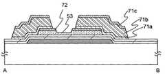
다음에, 레지스트 마스크(56)를 사용하여 미결정 반도체막(45), 버퍼층(54), 및 일 도전형을 부여하는 불순물이 첨가된 반도체막(55)을 에칭하여 분리하고, 도 5a에 도시하는 바와 같이, 미결정 반도체막(58), 버퍼층(62), 및 일 도전형을 부여하는 불순물이 첨가된 반도체막(63)을 형성한다. 그 후, 레지스트 마스크(56)를 제거한다. 또한, 도 5a(레지스트 마스크(56)는 제외함)는, 도 7a의 A-B 단면도에 상당한다.Next, the
미결정 반도체막(58), 버퍼층(62)의 단부 측면이 경사짐으로써, 버퍼층(62) 위에 형성되는 소스 영역 및 드레인 영역과 미결정 반도체막(58) 사이에 누설 전류가 생기는 것을 방지할 수 있다. 또한, 배선과 미결정 반도체막(58) 사이에 누설 전류가 생기는 것을 방지할 수 있다. 미결정 반도체막(58) 및 버퍼층(62)의 단부 측면의 경사 각도는, 30°내지 90°, 바람직하게는, 45° 내지 80°이다. 이러한 각도로 함으로써 단차 형상으로 인한 배선의 단선을 방지할 수 있다.Leakage of current between the source region and the drain region formed on the
다음에, 도 5b에 도시하는 바와 같이, 일 도전형을 부여하는 불순물이 첨가된 반도체막(63) 및 게이트 절연막(52b) 위에 도전막(65a 내지 65c)을 형성하고, 도전막(65a 내지 65c) 위에 레지스트 마스크(66)를 형성한다. 도전막(65a 내지 65c)은 스퍼터링법, CVD법, 인쇄법, 액적 토출법, 증착법 등을 사용하여 형성한다. 여기서는 도전막으로서, 도전막(65a 내지 65c)의 3층이 적층한 구조의 도전막을 제시하고, 도전막(65a, 65c)에 몰리브덴막, 도전막(65b)에 알루미늄막을 사용한 적층 도전막이나, 도전막(65a, 65c)에 티타늄막, 도전막(65b)에 알루미늄막을 사용한 적층 도전막을 제시한다. 도전막(65a 내지 65c)은 스퍼터링법이나 진공 증착법을 사 용하여 형성한다.Next, as shown in Fig. 5B,
도전막(65a 내지 65c)은 알루미늄, 구리, 혹은 실리콘, 티타늄, 네오디뮴, 스칸듐, 몰리브덴 등의 마이그레이션(migration) 방지 원소, 내열성 향상 원소, 혹은 힐록(hillock) 방지 원소가 첨가된 알루미늄 합금의 단층 혹은 적층으로 형성하는 것이 바람직하다. 또한, 일 도전형을 부여하는 불순물 원소가 첨가된 반도체막과 접하는 측의 막을, 티타늄, 탄탈, 몰리브덴, 텅스텐, 혹은 이들 원소의 질화물로 형성하고, 그 위에 알루미늄 혹은 알루미늄 합금을 형성한 적층 구조로 하여도 좋다. 또한, 알루미늄 혹은 알루미늄 합금의 위쪽 면 및 아래쪽 면을, 티타늄, 탄탈, 몰리브덴, 텅스텐, 혹은 이들 원소의 질화물로 끼운 적층 구조로 하여도 좋다.The
레지스트 마스크(66)는 레지스트 마스크(56)와 같은 방법으로 형성할 수 있다.The resist
다음에, 도 5c에 도시하는 바와 같이, 도전막(65a 내지 65c)을 부분적으로 에칭하여 한 쌍의 배선(71a 내지 71c)(소스 전극 및 드레인 전극으로서 기능함)을 형성한다. 여기서는, 제 3 포토마스크를 사용한 포토리소그래피 공정에 의하여 형성한 레지스트 마스크(66)를 사용하여 도전막(65a 내지 65c)을 웨트 에칭하면 도전막(65a 내지 65c)이 등방적으로 에칭된다. 결과적으로, 레지스트 마스크(66)보다 면적이 작은 배선(71a 내지 71c)을 형성할 수 있다.Next, as shown in Fig. 5C, the
다음에, 레지스트 마스크(66)를 사용하여 일 도전형을 부여하는 불순물 원소가 첨가된 반도체막(63)을 에칭하여 분리한다. 결과적으로, 도 6a에 도시하는 바와 같은, 한 쌍의 소스 영역 및 드레인 영역(72)을 형성할 수 있다. 또한, 상기 에칭 공정에 있어서, 버퍼층(62)도 부분적으로 에칭한다. 부분적으로 에칭된, 오목부가 형성된 버퍼층을 버퍼층(73)이라고 제시한다. 소스 영역 및 드레인 영역의 형성 공정과, 버퍼층의 오목부를 동일 공정으로 형성할 수 있다. 버퍼층의 오목부의 깊이를 버퍼층의 막 두께가 가장 두꺼운 영역의 1/2 내지 1/3로 함으로써, 소스 영역 및 드레인 영역의 거리를 뗄 수 있기 때문에, 소스 영역 및 드레인 영역 사이의 누설 전류를 저감시킬 수 있다. 그 후, 레지스트 마스크(66)를 제거한다.Next, the
다음에, 노출하는 버퍼층에 대미지가 생기지 않고, 또 상기 버퍼층에 대한 에칭 레이트(rate)가 낮은 조건으로 드라이 에칭한다. 이 공정에 의하여, 소스 영역 및 드레인 영역 사이에 있는 버퍼층 위의 에칭 잔사물, 레지스트 마스크의 잔사, 및 레지스트 마스크의 제거에 사용하는 장치 내의 오염원을 제거할 수 있고, 소스 영역 및 드레인 영역 사이의 절연을 확실하게 할 수 있다. 결과적으로, 박막 트랜지스터의 누설 전류를 저감시킬 수 있어, 오프 전류가 작고 내압이 높은 박막 트랜지스터를 제작할 수 있다. 또한, 에칭 가스로서 예를 들어, 염소 가스를 사용하면 좋다.Next, dry etching is performed under such a condition that there is no damage to the exposed buffer layer and the etching rate to the buffer layer is low. By this process, it is possible to remove the etching residues on the buffer layer between the source region and the drain region, the residue of the resist mask, and the contamination source in the apparatus used for removing the resist mask, and the insulation between the source region and the drain region . As a result, the leakage current of the thin film transistor can be reduced, and a thin film transistor having a small off current and high breakdown voltage can be manufactured. For example, chlorine gas may be used as the etching gas.
또한, 도 6a(레지스트 마스크(66)는 제외함)는 도 7b의 A-B 단면도에 상당한다. 도 7b에 도시하는 바와 같이, 소스 영역 및 드레인 영역(72)의 단부는 배선(71c)의 단부의 외측에 위치하는 것을 알 수 있다. 또한, 버퍼층(73)의 단부는 배선(71c) 및 소스 영역 및 드레인 영역(72)의 단부의 외측에 위치한다. 또한, 배선의 한쪽은 배선의 다른 쪽을 둘러싸는 형상(구체적으로는, U자형, C자형)이다. 따라서, 캐리어가 이동하는 영역의 면적을 증가시킬 수 있으므로, 전류량을 증가시 킬 수 있고, 박막 트랜지스터의 면적을 축소할 수 있다. 또한, 게이트 전극 위에 있어서, 미결정 반도체막과 배선이 중첩되기 때문에, 게이트 전극의 요철의 영향이 적고, 피복률의 저감 및 누설 전류의 발생을 억제할 수 있다.6A (excluding the resist mask 66) corresponds to a cross-sectional view taken along line A-B of FIG. 7B. As shown in Fig. 7B, it can be seen that the ends of the source region and the
상술한 공정에 의하여, 채널 에치형 박막 트랜지스터(74)를 형성할 수 있다.By the above-described process, the toothed
다음에, 도 6b에 도시하는 바와 같이, 배선(71a 내지 71c), 소스 영역 및 드레인 영역(72), 버퍼층(73), 미결정 반도체막(58), 및 게이트 절연막(52b) 위에 보호 절연막(76)을 형성한다. 보호 절연막(76)은 게이트 절연막(52a, 52b)과 마찬가지로 형성할 수 있다. 또한, 보호 절연막(76)은 대기 중에 부유하는 유기물이나 금속물, 수증기 등의 오염 불순물의 침입을 방지하는 막이고, 치밀한 막인 것이 바람직하다. 또한, 보호 절연막(76)에 질화실리콘막을 사용함으로써 버퍼층(73) 중의 산소 농도를 5×10¹⁹atoms/cm3 이하, 바람직하게는, 1×10¹⁹atoms/cm3 이하로 할 수 있어, 버퍼층(73)의 산화를 방지할 수 있다.6B, a protective insulating
다음에, 도 6c에 도시하는 바와 같이, 보호 절연막(76)에 제 4 포토마스크를 사용하여 형성한 레지스트 마스크를 사용하여 보호 절연막(76)을 부분적으로 에칭하여 콘택트 홀을 형성하고, 상기 콘택트 홀에 있어서 배선(71c)에 접하는 화소 전극(77)을 형성한다. 또한, 도 6c는 도 7c의 A-B의 단면도에 상당한다. 표시 소자의 화소 전극(77)에 접속되는 배선(71a 내지 71c)을 드레인 전극으로 하고, 반도체층 위에 있어서 상기 배선과 대향되는 배선(71a 내지 71c)을 소스 전극(소스 배선)으로 함으로써, 박막 트랜지스터의 Ion을 높게 할 수 있거나 혹은 반복 동작으로 인한 열화를 저감할 수 있다. 또한, 게이트 전극(51)과 드레인 전극으로서 기능하는 배선(71a 내지 71c) 사이에 생기는 기생 용량이 발생되기 어렵고, 화소 전극(77)에 전하를 축적하기 쉽다. 따라서, 상기 박막 트랜지스터를 액정 표시 장치에 사용하는 경우, 액정의 고속 동작이 가능하다.6C, a contact hole is formed by partially etching the protective insulating
화소 전극(77)은 산화텅스텐을 함유하는 인듐산화물, 산화텅스텐을 함유하는 인듐아연산화물, 산화티타늄을 함유하는 인듐산화물, 산화티타늄을 함유하는 인듐주석산화물, ITO, 인듐아연산화물, 산화실리콘을 첨가한 인듐주석산화물 등의 투광성을 갖는 도전성 재료를 사용할 수 있다.The
또한, 화소 전극(77)으로서 도전성 고분자(도전성 폴리머라고도 함)를 포함하는 도전성 조성물을 사용하여 형성할 수 있다. 도전성 조성물을 사용하여 형성한 화소 전극은 시트 저항이 10000Ω/□ 이하, 파장 550nm에 있어서의 투광률이 70% 이상인 것이 바람직하다. 또한, 도전성 조성물에 포함되는 도전성 고분자의 저항률이 0.1Ω·cm 이하인 것이 바람직하다.Further, the
도전성 고분자로서는, 소위 π전자 공역계 도전성 고분자를 사용할 수 있다. 예를 들어, 폴리아닐린 혹은 그 유도체, 폴리피롤 혹은 그 유도체, 폴리티오펜 혹은 그 유도체, 혹은 이들 2종 이상의 공중합체 등을 들 수 있다.As the conductive polymer, a so-called? -Electron conjugated conductive polymer can be used. For example, polyaniline or a derivative thereof, polypyrrole or a derivative thereof, polythiophene or a derivative thereof, or a copolymer of two or more thereof.
여기서는, 화소 전극(77)으로서는, 스퍼터링법에 의하여 ITO를 형성한 후, ITO 위에 레지스트를 도포한다. 다음에, 제 5 포토마스크를 사용하여 레지스트를 노광 및 현상하여 레지스트 마스크를 형성한다. 다음에, 레지스트 마스크를 사용하여 ITO를 에칭하여 화소 전극(77)을 형성한다.Here, as the
상술한 공정에 의하여, 박막 트랜지스터, 및 표시 장치에 사용할 수 있는 소자 기판을 형성할 수 있다.By the above-described steps, a thin film transistor and an element substrate usable in a display apparatus can be formed.
또한, 미결정 반도체막의 성막 처리에 있어서는, 실란 및 수소 외에, 반응 가스에 헬륨을 가하여도 좋다. 헬륨은 24.5eV로 모든 기체 중에서 가장 높은 이온화 에너지를 갖고 그 이온화 에너지보다 조금 낮은 약 20eV의 준위에 준안정 상태가 있기 때문에, 방전 지속 중에 있어서는, 이온화에 그 차이 약 4eV밖에 필요하지 않다. 따라서, 방전 개시 전압도 모든 기체 중 가장 낮은 값을 나타낸다. 이러한 특성에 의하여, 헬륨은 플라즈마를 안정적으로 유지할 수 있다. 또한, 균일한 플라즈마를 형성할 수 있기 때문에, 미결정 실리콘막을 퇴적하는 기판의 면적이 크게 되어도 플라즈마 밀도의 균일화를 도모할 효과가 있다.In addition, in the film forming process of the microcrystalline semiconductor film, helium may be added to the reaction gas in addition to silane and hydrogen. Since helium has the highest ionization energy of all gases at 24.5 eV and has a metastable state at a level of about 20 eV which is slightly lower than its ionization energy, only about 4 eV is needed for ionization during discharge. Therefore, the discharge starting voltage also shows the lowest value among all gases. With this characteristic, helium can stably maintain the plasma. Further, since a uniform plasma can be formed, even if the area of the substrate on which the microcrystalline silicon film is deposited is increased, uniformity of the plasma density can be achieved.
본 실시형태에 의하여, 결정성이 높은 미결정 반도체막을 채널 형성 영역으로서 사용한 박막 트랜지스터를 제작할 수 있다.According to the present embodiment, a thin film transistor using a microcrystalline semiconductor film having a high crystallinity as a channel forming region can be manufactured.
또한, 본 실시형태에서 제작하는 박막 트랜지스터의 채널 형성 영역은 결정성이 높은 미결정 반도체막으로 형성되기 때문에, 표시 장치의 구동 주파수를 높게 할 수 있고, 패널 크기의 대면적화나 화소의 고밀도화에도 충분히 대응할 수 있다. 또한, 대면적 기판에 상기 박막 트랜지스터를 제작할 수 있다.In addition, since the channel forming region of the thin film transistor fabricated in the present embodiment is formed of the microcrystalline semiconductor film having high crystallinity, the driving frequency of the display device can be increased, and it is possible to sufficiently cope with a large panel size and high density of pixels . Further, the thin film transistor can be fabricated on a large area substrate.
또한, 본 실시형태에서 제작하는 박막 트랜지스터는 채널 형성 영역인 미결정 반도체막과 소스 영역 및 드레인 영역인 일 도전형을 부여하는 불순물 원소가 첨가된 반도체막 사이에 버퍼층으로서 저항률이 높은 비정질 반도체막을 형성한다. 오프 전류는 상기 버퍼 영역을 흐르지만, 버퍼층은 고저항 영역이기 때문에, 오프 전류를 억제함과 함께 미결정 반도체막의 산화를 방지하는 기능도 가진다. 따라서, 오프 전류를 억제함과 함께, 채널 형성 영역에 있어서의 결함 저감으로 인한 온 전류의 상승을 도모할 수 있다.In the thin film transistor fabricated in this embodiment, an amorphous semiconductor film having a high resistivity as a buffer layer is formed between the microcrystalline semiconductor film as a channel forming region and the semiconductor film to which the impurity element imparting one conductivity type, which is a source region and a drain region, is added . Off current flows through the buffer region, but since the buffer layer is a high-resistance region, it has a function of suppressing the off current and preventing oxidation of the microcrystalline semiconductor film. Therefore, it is possible to suppress the off current and increase the on-current due to the reduction in the defect in the channel forming region.
다음에, 상기 형태와 상이한 박막 트랜지스터의 제작 방법에 대하여, 도 9a 내지 도 15c를 사용하여 설명한다. 여기서는, 상기 형태보다 포토마스크 수를 삭감할 수 있는 프로세스를 사용하여 박막 트랜지스터를 제작하는 공정에 대하여 제시한다.Next, a method of manufacturing a thin film transistor which is different from the above-described embodiment will be described with reference to FIGS. 9A to 15C. Here, a process for fabricating a thin film transistor using a process capable of reducing the number of photomasks is presented.
도 4a와 마찬가지로, 기판(50) 위에 도전막을 형성하고, 도전막 위에 레지스트를 도포하고, 제 1 포토마스크를 사용한 포토리소그래피 공정에 의하여 형성한 레지스트 마스크를 사용하여 도전막을 부분적으로 에칭하여 게이트 전극(51)을 형성한다. 다음에, 도 9a에 도시하는 바와 같이, 게이트 전극(51) 위에 게이트 절연막(52a, 52b)을 형성한다. 다음에, 미결정 반도체막(45), 버퍼층(54), 일 도전형을 부여하는 불순물 원소가 첨가된 반도체막(55), 및 도전막(65a 내지 65c)을 순차로 형성한다. 다음에, 도전막(65c) 위에 레지스트(80)를 도포한다.4A, a conductive film is formed on a
레지스트(80)는, 포지티브형 레지스트 혹은 네거티브형 레지스트를 사용할 수 있다. 여기서는, 포지티브형 레지스트를 사용하여 제시한다.As the resist 80, a positive type resist or a negative type resist can be used. Here, a positive type resist is used.
다음에, 제 2 포토마스크로서 다단계 마스크(159)를 사용하여, 레지스트(80)에 빛을 조사함으로써 레지스트(80)를 노광한다.Next, the resist 80 is exposed by irradiating the resist 80 with light using the
여기서, 다단계 마스크(159)를 사용한 노광에 대하여 도 10a 내지 도 10d를 사용하여 설명한다.Here, exposure using the
다단계 마스크란, 노광 부분, 중간 노광 부분, 및 미(未)노광 부분에 3개의 노광 레벨을 행할 수 있는 마스크이고, 한번의 노광 및 현상 공정에 의하여, 복수(대표적으로는 2종류)의 두께의 영역을 갖는 레지스트 마스크를 형성할 수 있다. 따라서, 다단계 마스크를 사용함으로써, 포토마스크 수를 삭감할 수 있다.The multistage mask is a mask capable of performing three exposure levels on the exposed portion, the intermediate exposed portion, and the unexposed portion, and is formed by a single exposure and development process to form a plurality of (typically two) A resist mask having a region can be formed. Therefore, by using a multistage mask, the number of photomasks can be reduced.
다단계 마스크의 대표적인 예로서는, 도 10a에 도시하는 바와 같은 그레이 톤 마스크(159a), 도 10c에 제시하는 바와 같은 하프 톤 마스크(159b)가 있다.As a representative example of the multistage mask, there are a gray-
도 10a에 도시하는 바와 같이, 그레이 톤 마스크(159a)는 투광성을 갖는 기판(163) 및 그 위에 형성되는 차광부(164) 및 회절 격자(165)로 구성된다. 차광부(164)는 빛 투과율이 0%이다. 한편, 회절 격자(165)는 슬릿, 도트, 메쉬 등의 광 투과부의 간격을, 노광에 사용되는 빛의 해상도 한계 이하의 간격으로 함으로써 빛의 투과율을 제어할 수 있다. 또한, 회절 격자(165)는 주기적인 슬릿, 도트, 메쉬, 혹은 비주기적인 슬릿, 도트, 메쉬 중의 어느 쪽이라도 사용할 수 있다.As shown in Fig. 10A, the gray-
투광성을 갖는 기판(163)은 석영 등의 투광성을 갖는 기판을 사용할 수 있다. 차광부(164) 및 회절 격자(165)는 크롬이나 산화크롬 등의 빛을 흡수하는 차광 재료를 사용하여 형성할 수 있다.A substrate having translucency such as quartz can be used for the
그레이 톤 마스크(159a)에 노광광을 조사한 경우, 도 10b에 도시하는 바와 같이, 차광부(164)에서는 빛 투과율(166)은 0%이며, 차광부(164) 및 회절 격자(165)가 형성되지 않는 영역에서는 빛 투과율(166)은 100%이다. 또한, 회절 격자(165)는 10% 내지 70%의 범위로 조정할 수 있다. 회절 격자(165)의 빛 투과율의 조정은 회절 격자의 슬릿, 도트, 혹은 메쉬의 간격 및 피치를 조정함으로써 행할 수 있다.10B, the
도 10c에 도시하는 바와 같이, 하프 톤 마스크(159b)는 투광성을 갖는 기판(163) 및 그 위에 형성되는 반 투과부(167) 및 차광부(168)로 구성된다. 반 투과부(167)는 MoSiN, MoSi, MoSiO, MoSiON, CrSi 등을 사용할 수 있다. 차광부(168)는 크롬이나 산화크롬 등의 빛을 흡수하는 차광 재료를 사용하여 형성할 수 있다.As shown in Fig. 10C, the
하프 톤 마스크(159b)에 노광광을 조사한 경우, 도 10d에 도시하는 바와 같이, 차광부(168)에서는 빛 투과율(169)은 0%이며, 차광부(168) 및 반 투과부(167)가 형성되지 않는 영역에서는 빛 투과율(169)은 100%이다. 또한, 반 투과부(167)는 10% 내지 70%의 범위로 조정할 수 있다. 반 투과부(167)의 빛 투과율의 조정은 반 투과부(167)의 재료를 조정함으로써 행할 수 있다.The
다단계 마스크를 사용하여 노광한 후 현상함으로써, 도 9b에 도시하는 바와 같이, 막 두께가 상이한 영역을 갖는 레지스트 마스크(81)를 형성할 수 있다.By exposure using a multistage mask and then development, a resist
다음에, 레지스트 마스크(81)에 의하여, 미결정 반도체막(45), 버퍼층(54), 일 도전형을 부여하는 불순물 원소가 첨가된 반도체막(55), 및 도전막(65a 내지 65c)을 에칭하여 분리한다. 결과적으로, 도 11a에 도시하는 바와 같은, 미결정 반도체막(58), 버퍼층(62), 일 도전형을 부여하는 불순물 원소가 첨가된 반도체막(63), 및 도전막(85a 내지 85c)을 형성할 수 있다. 또한, 도 11a(레지스트 마스크(81)를 제외함)는 도 15a의 A-B의 단면도에 상당한다.Next, the
다음에, 레지스트 마스크(81)를 애싱(ashing)한다. 결과적으로, 레지스트의 면적이 축소되고, 두께가 얇게 된다. 이 때, 막 두께가 얇은 영역의 레지스트(게이트 전극(51)과 부분적으로 중첩하는 영역)는 제거되고, 도 11a에 도시하는 바와 같이, 분리된 레지스트 마스크(86)를 형성할 수 있다.Next, the resist
다음에, 레지스트 마스크(86)를 사용하여, 도전막(85a 내지 85c)을 에칭하여 분리한다. 결과적으로, 도 11b에 도시하는 바와 같은, 한 쌍의 배선(92a 내지 92c)을 형성할 수 있다. 레지스트 마스크(86)를 사용하여 도전막(85a 내지 85c)을 웨트 에칭하면, 도전막(85a 내지 85c)이 등방적으로 에칭된다. 결과적으로, 레지스트 마스크(86)보다 면적이 작은 배선(92a 내지 92c)을 형성할 수 있다.Next, using the resist
다음에, 레지스트 마스크(86)를 사용하여 일 도전형을 부여하는 불순물 원소가 첨가된 반도체막(63)을 에칭하여, 한 쌍의 소스 영역 및 드레인 영역(88)을 형성한다. 또한, 상기 에칭 공정에 있어서, 버퍼층(62)도 부분적으로 에칭된다. 부분적으로 에칭된 버퍼층을 버퍼층(87)이라고 기재한다. 또한, 버퍼층(87)에는 오목부가 형성된다. 소스 영역 및 드레인 영역과 버퍼층의 오목부를 동일 공정으로 형성할 수 있다. 여기서는, 버퍼층(87)의 일부분이 레지스트 마스크(81)와 비교하여 면적이 축소된 레지스트 마스크(86)로 부분적으로 에칭되기 때문에, 소스 영역 및 드레인 영역(88)의 외측에 버퍼층(87)이 돌출한 형상이 된다. 또한, 배선(92a 내지 92c)의 단부와 소스 영역 및 드레인 영역(88)의 단부는 일치하지 않고 어긋나고, 배선(92a 내지 92c)의 단부의 외측에, 소스 영역 및 드레인 영역(88)의 단부가 형성된다. 그 후, 레지스트 마스크(86)를 제거한다.Next, the
다음에, 노출하는 버퍼층에 대미지를 주지 않고 또 상기 버퍼층에 대한 에칭 레이트가 낮은 조건으로 드라이 에칭하여도 좋다. 이 공정에 의하여, 소스 영역 및 드레인 영역 사이에 있는 버퍼층 위의 에칭 잔사물, 레지스트 마스크의 잔사, 및 레지스트 마스크의 제거에 사용하는 장치 내의 오염원을 제거할 수 있고, 소스 영역 및 드레인 영역 사이의 절연을 확실하게 할 수 있다. 결과적으로, 박막 트랜지스터의 누설 전류를 저감할 수 있으므로, 오프 전류가 작고 내압이 높은 박막 트랜지스터를 제작할 수 있다. 또한, 에칭 가스로서, 예를 들어, 염소를 함유하는 가스, 불소를 함유하는 가스 등을 사용하면 좋다.Next, dry etching may be performed under the condition that the buffer layer to be exposed is not damaged and the etching rate to the buffer layer is low. By this process, it is possible to remove the etching residues on the buffer layer between the source region and the drain region, the residue of the resist mask, and the contamination source in the apparatus used for removing the resist mask, and the insulation between the source region and the drain region . As a result, since the leakage current of the thin film transistor can be reduced, a thin film transistor having a small off current and a high breakdown voltage can be manufactured. As the etching gas, for example, a gas containing chlorine or a gas containing fluorine may be used.
도 11c에 도시하는 바와 같이, 배선(92a 내지 92c)의 단부와 소스 영역 및 드레인 영역(88)의 단부는 일치하지 않고 어긋난 형상이 됨으로써, 배선(92a 내지 92c)의 단부의 거리가 떨어지기 때문에, 배선 사이의 누설 전류나 단락을 방지할 수 있다. 따라서, 역 스태거형 박막 트랜지스터를 제작할 수 있다.The end portions of the
상술한 공정에 의하여, 채널 에치형 박막 트랜지스터(83)를 형성할 수 있다. 또한, 2장의 포토마스크를 사용하여 박막 트랜지스터를 형성할 수 있다.By the above-described process, the toothed
다음에, 도 12a에 도시하는 바와 같이, 배선(92a 내지 92c), 소스 영역 및 드레인 영역(88), 버퍼층(87), 미결정 반도체막(58), 및 게이트 절연막(52b) 위에 보호 절연막(76)을 형성한다.12A, a protective insulating
다음에, 제 3 포토마스크를 사용하여 형성한 레지스트 마스크를 사용하여 보호 절연막(76)을 부분적으로 에칭하여 콘택트 홀을 형성한다. 다음에, 상기 콘택트 홀에 있어서 배선(71c)에 접하는 화소 전극(77)을 형성한다. 여기서는, 스퍼터링법에 의하여 ITO를 형성한 후, ITO 위에 레지스트를 도포하고, 제 4 포토마스크 를 사용하여 레지스트를 노광 및 현상하여 레지스트 마스크를 형성하고, 레지스트 마스크를 사용하여 ITO를 에칭하여 화소 전극(77)을 형성한다. 또한, 도 12b는 도 15c의 A-B의 단면도에 상당한다.Next, the protective insulating
상술한 공정에 의하여, 박막 트랜지스터, 및 상기 박막 트랜지스터를 갖고, 표시 장치에 사용할 수 있는 소자 기판을 형성할 수 있다.According to the above-described processes, a thin film transistor and an element substrate having the thin film transistor and usable in a display apparatus can be formed.
다음에, 1장의 포토마스크로 콘택트 홀과 용량 소자를 형성할 수 있는 공정에 대하여 이하에 제시한다. 여기서는, 도 15a 내지 도 15c의 C-D의 단면도를 도시한다.Next, a process for forming a contact hole and a capacitor element using a single photomask will be described below. Here, a sectional view taken along a line C-D in Figs. 15A to 15C is shown.
도 12a에 도시하는 공정 후, 도 13a에 도시하는 바와 같이, 보호 절연막(76) 위에 절연막(101)을 형성한다. 여기서는, 감광성의 유기 수지를 사용하여 절연막(101)을 형성한다. 다음에, 다단계 마스크(160)를 사용하여 절연막(101)을 감광한 후 현상하여, 도 13b에 도시하는 바와 같이, 박막 트랜지스터의 배선을 덮는 보호 절연막(76)을 노출하는 오목부(111a)와 용량 배선(51c) 위에 오목부(111b)를 형성한다. 여기서는, 박막 트랜지스터의 배선에서 절연막(101)을 100%의 투과광으로 노광할 수 있고, 또한, 용량 배선(51c) 위에서는 절연막(101)을 10% 내지 70%로 감쇠된 투과광으로 노광할 수 있는 다단계 마스크(160)를 사용한다.After the step shown in Fig. 12A, the insulating
다음에, 보호 절연막(76) 및 오목부를 갖는 절연막(102)을 전체적으로 에칭(에치백)하여 보호 절연막(76a)을 부분적으로 에칭하여, 도 14a에 도시하는 바와 같이, 배선을 노출하는 콘택트 홀(112a)을 형성함과 함께, 용량 배선(51c) 위에 오목부(112b)를 갖는 절연막(103)을 형성한다.Next, the protective insulating
다음에, 절연막(103)을 애싱하고, 콘택트 홀(112a) 및 오목부(112b)의 면적을 넓히고, 콘택트 홀(113a) 및 오목부(113b)를 갖는 절연막(104)을 형성한다. 또한, 보호 절연막(76)은 감광성 유기 수지로 형성되지 않고, 무기 절연막으로 형성되기 때문에, 애싱되지 않는다. 따라서, 배선 위에는 상면 형상이 2중의 고리가 되는 콘택트 홀(113a)이 형성된다.Next, the insulating
그 후, 화소 전극(77)을 형성함과 함께, 용량 배선(51c), 게이트 절연막(52a, 52b), 보호 절연막(76a), 및 화소 전극(77)으로 구성되는 용량 소자(105)를 형성할 수 있다.Thereafter, a
상술한 공정에 의하여, 1장의 다단계 마스크에 의하여 화소 전극 및 배선을 접속하는 콘택트 홀을 형성함과 함께, 용량 소자를 형성할 수 있다.According to the above-described process, a contact hole for connecting the pixel electrode and the wiring with one multistage mask can be formed and a capacitive element can be formed.
또한, 도 5c의 배선(71a 내지 71c) 혹은 도 11b의 배선(92a 내지 92c)을 형성한 후, 레지스트 마스크(66 혹은 86)를 제거하고, 배선(71a 내지 71c 혹은 92a 내지 92c)을 마스크로서 사용하여 일 도전형을 부여하는 불순물 원소가 첨가된 반도체막(63)을 에칭하여도 좋다. 결과적으로, 배선(71a 내지 71c 혹은 92a 내지 92c)과, 소스 영역 및 드레인 영역(72 혹은 88)의 단부가 일치한 박막 트랜지스터를 형성할 수 있다. 여기서는, 도 5c의 레지스트 마스크(66)를 제거한 후, 배선(71a 내지 71c)을 마스크로서 사용하여 일 도전형을 부여하는 불순물 원소가 첨가된 반도체막(63)을 에칭하여, 소스 영역 및 드레인 영역(89)의 단부와 배선(71a 내지 71c)의 단부가 일치하는 박막 트랜지스터를 도 16에 도시한다.After the
또한, 본 실시형태에서는 채널 에치형 박막 트랜지스터를 사용하여 제시하지 만, 채널 보호형 박막 트랜지스터의 채널 형성 영역에 미결정 반도체막을 사용할 수 있다.In this embodiment mode, a trench type thin film transistor is used for a channel, but a microcrystalline semiconductor film can be used for a channel forming region of the channel protection type thin film transistor.
구체적으로는, 도 4a에 도시하는 바와 같이, 기판(50) 위에 게이트 전극(51)을 형성하고, 게이트 전극(51) 위에 게이트 절연막(52a, 52b)을 형성한다. 다음에, 미결정 반도체막(45)을 형성한다.4A, the
도 4e에 도시하는 바와 같이, 미결정 반도체막(45) 위에 버퍼층(54)을 형성한다. 다음에, 버퍼층(54)이고, 또 게이트 전극(51)에 중첩하는 영역에 채널 보호막을 형성한다. 채널 보호막은 질화실리콘막, 산화실리콘막, 질산화실리콘막, 산질화실리콘막을 형성한 후, 포토리소그래피 공정에 의하여 선택적으로 에칭하여 형성할 수 있다. 혹은, 폴리이미드, 아크릴, 혹은 실록산을 함유하는 조성물을 토출하고 소성하여 형성할 수 있다. 다음에, 일 도전형을 부여하는 불순물이 첨가된 반도체막 및 도전막을 순차로 형성한다. 다음에, 포토리소그래피 공정에 의하여 형성한 레지스트 마스크를 사용하여, 도전막, 일 도전형을 부여하는 불순물 원소가 첨가된 반도체막, 버퍼층, 도너로서 기능하는 불순물 원소를 함유하지 않는 미결정 반도체막, 도너로서 기능하는 불순물 원소를 함유하는 미결정 반도체막을 에칭하여 분리한다. 결과적으로, 도 17에 도시하는 바와 같이, 미결정 반도체막(61), 버퍼층(73), 소스 영역 및 드레인 영역(72), 및 소스 전극 및 드레인 전극으로서 기능하는 배선(71a 내지 71c)을 형성한다. 또한, 부분적으로 오목부를 갖는 채널 보호막(82)을 형성한다.The
상술한 공정에 의하여 채널 보호형 박막 트랜지스터를 형성할 수 있다.The channel-protective thin film transistor can be formed by the above-described processes.
또한, 본 실시형태에서는 미결정 반도체막 위에 버퍼층을 형성한 박막 트랜지스터를 사용하여 제시하지만, 도 18에 도시하는 바와 같이, 미결정 반도체막(53)에 접하는 소스 영역 및 드레인 영역(72)을 갖는 박막 트랜지스터를 사용할 수 있다. 상기 박막 트랜지스터의 경우, 분리된 소스 영역 및 드레인 영역(72)을 형성할 때, 미결정 반도체막이 부분적으로 에칭되기 때문에 미결정 반도체막(53)은 오목부를 가진다.18, a thin film transistor having a source region and a
또한, 도 4a에 제시하는 박막 트랜지스터의 게이트 절연막(52a, 52b) 대신에, 도 19에 도시하는 바와 같이, 3층의 게이트 절연막(52a, 52b, 52c)을 형성하여도 좋다. 3층의 게이트 절연막(52c)으로서 두께 1nm 내지 5nm 정도의 질화실리콘막 혹은 질산화실리콘막을 형성할 수 있다.Note that three
3층째의 게이트 절연막으로서 형성하는 두께 1nm 내지 5nm 정도의 질화실리콘막 혹은 질산화실리콘막은 플라즈마 CVD법에 의하여 형성할 수 있다. 또한, 게이트 절연막(52b)에 대하여, 고밀도 플라즈마를 사용하여 질화 처리하여 게이트 절연막(52b) 표면에 질화실리콘층을 형성할 수 있다. 고밀도 플라즈마를 사용하여 질화함으로써, 더 높은 농도의 질소를 함유하는 질화실리콘층을 얻을 수도 있다. 고밀도 플라즈마는 높은 주파수의 마이크로파, 예를 들어, 2.45GHz를 사용함으로써 생성된다. 저전자 온도가 특징인 고밀도 플라즈마는 활성종(活性種)의 운동 에너지가 낮기 때문에, 종래의 플라즈마 처리와 비교하여 플라즈마 대미지가 적고 결함이 적은 층을 형성할 수 있다. 또한, 게이트 절연막(52b)의 표면 거칠기를 작게 할 수 있기 때문에, 캐리어 이동도를 크게 할 수 있다.A silicon nitride film or silicon oxynitride film having a thickness of about 1 nm to 5 nm, which is formed as the third-layer gate insulating film, can be formed by the plasma CVD method. Further, the
또한, 게이트 절연막(52a, 52b)을 형성한 후, 성막 장치의 반응실 내에 실리콘 혹은 게르마늄을 함유하는 퇴적성 가스를 흘리고, 반응실 내에 잔존하는 게이트 절연막(52a, 52b)의 원료 가스, 특히 산소, 질소를 함유하는 가스를 제거하는 것이 바람직하다. 상기 공정에 의하여, 반응실 내의 산소 농도, 질소 농도를 저감할 수 있고, 이후 형성하는 미결정 반도체막의 산소 농도, 질소 농도를 저감할 수 있다. 결과적으로, 결함이 적은 미결정 반도체막을 형성할 수 있다.After forming the
또한, 마찬가지로, 게이트 절연막(52a, 52b)을 형성한 후, 성막 장치의 반응실 내에 도너로서 기능하는 불순물 원소를 함유하는 기체를 흘리고, 반응실 내벽 및 게이트 절연막(52b) 표면에 도너로서 기능하는 불순물 원소를 흡착시켜도 좋다. 결과적으로, 이후 형성되는 게이트 절연막(52c) 및 반도체막에 도너로서 기능하는 불순물 원소를 참가할 수 있다. 즉, 도너로서 기능하는 불순물 원소를 함유하는 미결정 반도체막을 형성할 수 있다.Similarly, after forming the
또한, 본 실시형태에 있어서는 미결정 반도체막의 형성 방법으로서 실시형태1을 사용하여 형성하지만, 적절히 실시형태 2 혹은 실시형태 3을 적용할 수 있다.In this embodiment mode, the method of forming a microcrystalline semiconductor film is formed by using
예를 들어, 실시형태 3에서 제시하는 바와 같은, 도너로서 기능하는 불순물 원소를 함유하는 미결정 반도체막을 채널 형성 영역에 사용함으로써, 축적(accumulate)형 박막 트랜지스터를 형성할 수 있고, 게이트 절연막(52b) 및 미결정 반도체막(58) 계면의 결정성을 높일 수 있다.For example, an accumulation type thin film transistor can be formed by using a microcrystalline semiconductor film containing an impurity element serving as a donor in the channel forming region as shown in
다음에, 상기 반응실이 적용되는 플라즈마 CVD 장치의 일례로서, 게이트 절연막, 미결정 반도체막의 형성에 적합한 구성의 일례를 제시한다.Next, as an example of a plasma CVD apparatus to which the above reaction chamber is applied, an example of a structure suitable for forming a gate insulating film and a microcrystalline semiconductor film is presented.
도 8은 복수의 반응실을 구비한 멀티 챔버 플라즈마 CVD장치의 일례를 도시한다. 이 장치는 공통실(423), 로드/언로드실(422), 제 1 반응실(400a), 제 2 반응실(400b), 제 3 반응실(400c), 제 4 반응실(400d)을 구비한 구성이다. 로드/언로드실(422)의 카세트에 장전되는 기판은 공통실(423)의 반송 기구(426)에 의하여 각 반응실에 반출입되는 매엽식의 구성이다. 공통실(423)과 각 반응실 사이에는 게이트 밸브(425)가 구비되어 각 반응실에서 행해지는 처리가 서로 간섭하지 않도록 구성된다.Fig. 8 shows an example of a multi-chamber plasma CVD apparatus having a plurality of reaction chambers. The apparatus includes a
각 반응실은 형성하는 박막의 종류에 따라 구분된다. 예를 들어, 제 1 반응실(400a)에서 게이트 절연막 등의 절연막을 형성하고, 제 2 반응실(400b)에서 채널을 형성하는 미결정 반도체막을 형성하고, 제 3 반응실(400c)에서 버퍼층을 형성하고, 제 4 반응실(400d)에서 소스 및 드레인을 형성하는 일 도전형을 부여하는 불순물 원소가 첨가된 반도체막을 형성하는 반응실로서 충당된다. 물론, 반응실 수는 이것에 한정되지 않고, 필요에 따라 임의로 증감할 수 있다. 또한, 하나의 반응실에서 하나의 막을 형성하여도 좋고, 하나의 반응실에서 복수의 막을 형성하도록 구성하여도 좋다.Each reaction chamber is classified according to the kind of the thin film to be formed. For example, an insulating film such as a gate insulating film is formed in the
각 반응실에는 배기 수단으로서 터보 분자 펌프(419)와 드라이 펌프(420)가 접속된다. 배기 수단은 이들 진공 펌프의 조합에 한정되지 않고, 대략 10-1Pa 내지 10-5Pa의 진공도까지 배기할 수 있는 것이라면 다른 진공 펌프를 적용할 수 있다. 배기 수단과 각 반응실 사이에는 버터플라이 밸브(417)가 형성되고 이것으로 진공 배기를 차단시킬 수 있고, 컨덕턴스 밸브(418)에 의하여 배기 속도를 제어함으로써 반응실 각각의 압력을 조절할 수 있다.In each reaction chamber, a turbo
또한, 반도체막, 미결정 반도체막을 형성하는 제 2 반응실(400b)은 초고진공까지 진공 배기하는 크라이오 펌프(421)가 연결되어도 좋다. 크라이오 펌프(421)를 사용함으로써 반응실의 압력을 10-5Pa보다 낮은 압력인 초고진공 상태로 할 수 있다. 본 실시형태에서는, 반응실 내를 10-5Pa보다 낮은 압력인 초고진공 상태로 함으로써 미결정 반도체막 중의 산소 농도 및 질소 농도의 저감에 효과적이다. 결과적으로, 특히, 미결정 반도체막(45)에 함유되는 산소 농도를 1×10¹⁶atoms/cm3 이하로 할 수 있다. 미결정 반도체막 중의 산소 농도 및 질소 농도를 저감함으로써 막 중의 결함을 저감하고 결정성을 높일 수 있기 때문에, 캐리어의 이동도를 향상시킬 수 있다.The
가스 공급 수단(408)은 실란으로 대표되는 반도체 재료 가스 혹은 희소 가스 등 프로세스에 사용하는 가스가 충전되는 실린더(410), 스톱 밸브(412), 마스 플로 컨트롤러(413) 등으로 구성된다. 가스 공급 수단(408g)은 제 1 반응실(400a)에 접속되고 게이트 절연막을 형성하기 위한 가스를 공급한다. 가스 공급 수단(408i)은 제 2 반응실(400b)에 접속되고, 미결정 반도체막용의 가스를 공급한다. 가스 공급 수단(408b)은 제 3 반응실(400c)에 접속되고 버퍼층용의 가스를 공급한다. 가스 공금 수단(408n)은 제 4 반응실(400d)에 접속되고, 예를 들어, n형 반도체막용의 가스를 공급한다. 또한, 도너로서 기능하는 불순물 원소를 함유하는 기체의 하나 인 포스핀은 제 1 반응실(400a), 제 2 반응실(400b)에 접속되어 공급되어도 좋다. 가스 공급 수단(408a)은 아르곤을 공금하고, 가스 공급 수단(408f)은 반응실 내의 클리닝에 사용되는 에칭 가스를 공급하는 계통이며, 이들은 각 반응실 공통의 라인으로서 구성된다.The gas supply means 408 is composed of a
각 반응실에는 플라즈마를 형성하기 위한 고주파 전력 공급 수단이 연결된다. 고주파 전력 공급 수단은 고주파 전원(404)과 정합기(406)가 포함된다.High-frequency power supply means for forming a plasma is connected to each reaction chamber. The high frequency power supply means includes a high
각 반응실은 형성하는 박막의 종류에 따라 구별하여 쓸 수 있다. 박막 각각은 적절한 성막 온도가 있으므로, 반응실을 개별로 구별함으로써 성막 온도의 관리가 용이하게 된다. 또한, 같은 종류의 막을 반복하여 형성할 수 있으므로, 성막 이력에 관계하는 잔류 불순물의 영향을 배제할 수 있다. 특히, 미결정 반도체막에 도너로서 기능하는 불순물 원소가 포함되는 경우, 상기 도너로서 기능하는 불순물 원소를 버퍼층에 혼입시키는 것을 회피할 수 있다. 결과적으로, 버퍼층의 불순물 원소의 농도를 저감할 수 있고, 박막 트랜지스터의 오프 전류를 저감할 수 있다.Each reaction chamber can be used separately depending on the kind of the thin film to be formed. Since each thin film has an appropriate film forming temperature, it is easy to manage the film forming temperature by separately discriminating the reaction chambers. Further, since the same kind of film can be repeatedly formed, the influence of residual impurities related to the deposition history can be excluded. Particularly, when the microcrystalline semiconductor film contains an impurity element which functions as a donor, mixing of the impurity element serving as the donor into the buffer layer can be avoided. As a result, the concentration of the impurity element in the buffer layer can be reduced, and the off current of the thin film transistor can be reduced.
또한, 동일 반응실 내에 있어서, 반도체막, 미결정 반도체막, 버퍼층, 일 도전형을 부여하는 불순물 원소가 첨가된 반도체막을 연속적으로 형성하여도 좋다. 구체적으로는, 게이트 절연막이 형성된 기판을 반응실에 반입하고, 거기서 반도체막, 미결정 반도체막, 버퍼층, 및 일 도전형을 부여하는 불순물 원소가 첨가된 반도체막을 연속적으로 형성한다. 그 후, 반응실로부터 기판을 반출한 후, 반응실 내를 불소 라디칼 등으로 클리닝하는 것이 바람직하다.In addition, a semiconductor film, a microcrystalline semiconductor film, a buffer layer, and a semiconductor film to which an impurity element imparting one conductivity type is added may be continuously formed in the same reaction chamber. Specifically, a substrate on which a gate insulating film is formed is carried into a reaction chamber, and a semiconductor film to which a semiconductor film, a microcrystalline semiconductor film, a buffer layer, and an impurity element imparting one conductivity type are added is successively formed. Thereafter, after the substrate is taken out from the reaction chamber, it is preferable to clean the inside of the reaction chamber with a fluorine radical or the like.
본 실시형태에 의하여, 결정성이 높은 미결정 반도체막을 갖는 역 스태거형 박막 트랜지스터, 및 그것을 갖는 소자 기판을 제작할 수 있다.According to the present embodiment, an inverted stagger type thin film transistor having a microcrystalline semiconductor film with high crystallinity and an element substrate having the inverted stagger type thin film transistor can be manufactured.
또한, 본 실시형태에서는 박막 트랜지스터로서 역 스태거형 박막 트랜지스터를 사용하여 설명하지만, 이것에 한정되지 않고, 순 스태거형 박막 트랜지스터, 톱 게이트형 박막 트랜지스터 등에도 적용할 수 있다. 구체적으로는, 하지막으로서 기능하는 절연막 혹은 미결정 반도체막에 도너로서 기능하는 불순물 원소를 함유시켜 미결정 반도체막 위에 게이트 절연막 및 게이트 전극을 형성하면, 절연막과의 계면의 결정성이 높아진 미결정 반도체막을 갖는 박막 트랜지스터를 제작할 수 있다.In this embodiment mode, a reverse stagger type thin film transistor is used as a thin film transistor. However, the present invention is not limited to this, and can be applied to a net stagger type thin film transistor, a top gate type thin film transistor, and the like. Specifically, when an insulating film or a gate electrode is formed on a microcrystalline semiconductor film by containing an impurity element serving as a donor in an insulating film or a microcrystalline semiconductor film functioning as a base film, the microcrystalline semiconductor film having an increased crystallinity at the interface with the insulating film A thin film transistor can be manufactured.
(실시형태 5)(Embodiment 5)
본 실시형태에서는 실시형태 4의 박막 트랜지스터의 미결정 반도체막(45)의 형성 공정에 있어서, 실시형태 3에 제시하는 바와 같은 도너로서 기능하는 불순물 원소를 함유하는 미결정 반도체막의 형성 공정을 사용한 박막 트랜지스터의 구조에 대하여 이하에 제시한다.In the present embodiment, in the step of forming the
도 6a에 제시한 박막 트랜지스터(74)의 미결정 반도체막이 농도가 높은 도너로서 기능하는 불순물 원소를 함유하는 미결정 반도체막의 경우, 미결정 반도체막과 배선(71a 내지 71c) 사이에 누설 전류가 생기기 쉽다. 따라서, 누설 전류를 저감할 수 있는 구조를 이하에 제시한다.The microcrystalline semiconductor film of the
실시형태 4와 마찬가지로, 도 4a에 제시하는 바와 같이, 기판(50) 위에 게이트 전극(51) 및 게이트 절연막(52a, 52b)을 형성한다. 다음에, 실시형태 3과 같은 공정을 거쳐, 게이트 절연막(52a, 52b) 위에 도너로서 기능하는 불순물 원소를 함 유하는 미결정 반도체막을 형성하고, 상기 미결정 반도체막 위에 버퍼층(54) 및 일 도전형을 부여하는 불순물이 첨가된 반도체막(55)을 도 4e에 제시하는 바와 같이 형성한다. 다음에, 일 도전형을 부여하는 불순물이 첨가된 반도체막(55) 위에 레지스트 마스크(56)를 형성하고, 일 도전형을 부여하는 불순물이 첨가된 반도체막, 버퍼층, 및 도너로서 기능하는 불순물 원소를 함유하는 미결정 반도체막을 에칭하여 도 29a 내지 도 29c에 도시하는 바와 같이, 도너로서 기능하는 불순물 원소를 함유하는 미결정 반도체막(59), 버퍼층(62), 및 일 도전형을 부여하는 불순물이 첨가된 반도체막(63)을 형성한다.The
다음에, 도 29b에 도시하는 바와 같이, 일 도전형을 부여하는 불순물이 첨가된 반도체막(63), 및 게이트 절연막(52b) 위에 절연막(67)을 형성한다. 절연막(67)은 게이트 절연막(52a, 52b)와 같은 재료를 적절히 사용하여 형성할 수 있다.Next, as shown in Fig. 29B, a
다음에, 절연막(67) 위에 레지스트 마스크(68)을 형성한다. 레지스트 마스크는 절연막(67)을 부분적으로 에칭함으로써, 이후 형성하는 배선이 도너로서 기능하는 불순물 원소를 함유하는 미결정 반도체막(59)과 접하는 것을 방지하고, 또 일 도전형을 부여하는 불순물이 첨가된 반도체막(63)과 접하는 절연막을 형성하기 위한 것이기 때문에, 일 도전형을 부여하는 불순물이 첨가된 반도체막(63)보다 위쪽 면 면적이 작은 형상인 것이 바람직하다.Next, a resist
다음에, 레지스트 마스크(68)를 사용하여 절연막(67)을 에칭하여, 도 29c에 도시하는 바와 같이, 일 도전형을 부여하는 불순물이 첨가된 반도체막(63)의 단부 를 덮는 절연막(67a)을 형성한다.Next, as shown in Fig. 29C, the insulating
다음에, 도 30a에 도시하는 바와 같이, 절연막(67a), 및 일 도전형을 부여하는 불순물이 첨가된 반도체막(63) 위에 실시형태 4와 마찬가지로 도전막(65a 내지 65c)을 형성하고 도전막(65a 내지 65c) 위에 레지스트 마스크(66)를 형성한다.Next, as shown in Fig. 30A,
다음에, 도 30b에 도시하는 바와 같이, 레지스트 마스크(66)를 사용하여 도전막(65a 내지 65c)을 에칭하여 배선(71a 내지 71c)을 형성한다.Next, as shown in Fig. 30B, the
다음에, 레지스트 마스크(66)를 사용하여 일 도전형을 부여하는 불순물 원소가 첨가된 반도체막(63)을 에칭하여 분리한다. 결과적으로, 도 31a에 도시하는 바와 같은, 한 쌍의 소스 영역 및 드레인 영역(72)을 형성할 수 있다. 또한, 상기 에칭 공정에 있어서, 버퍼층(62)도 부분적으로 에칭한다. 부분적으로 에칭된, 오목부가 형성된 버퍼층을 버퍼층(73)이라고 기재한다.Next, the
상술한 공정에 의하여, 채널 에치형 박막 트랜지스터(31)를 형성할 수 있다. 도너로서 기능하는 불순물 원소를 함유하는 미결정 반도체막(59)과 배선(71a 내지 71c)이 절연막(67a)으로 절연되기 때문에, 도너로서 기능하는 불순물 원소를 함유하는 미결정 반도체막(59)과 배선(71a 내지 71c) 사이에서 생기는 누설 전류를 저감할 수 있다. 따라서, 오프 전류가 낮은 박막 트랜지스터를 형성할 수 있다.By the above-described process, the toothed
다음에, 배선(71c) 및 게이트 절연막(52b) 위에, 실시형태 4와 마찬가지로 절연막(76)을 형성한다. 다음에, 절연막(76)을 부분적으로 에칭하여 콘택트 홀을 형성함과 함께, 배선(71c)의 일부분을 노출한다. 다음에, 콘택트 홀에 실시형태 4와 마찬가지로, 도 31c에 도시하는 바와 같이, 화소 전극(77)을 형성한다. 상술 한 공정에 의하여 표시 기판을 제작할 수 있다.Next, an insulating
상술한 공정에 의하여, 오프 전류가 낮은 박막 트랜지스터를 갖는 표시 기판을 제작할 수 있다. 또한, 상기 표시 기판을 사용함으로써 콘트라스트가 높은 표시 장치를 제작할 수 있다.By the above-described process, a display substrate having a thin film transistor with a low off current can be manufactured. Further, by using the display substrate, a display device with high contrast can be manufactured.
다음에, 박막 트랜지스터(31)와 마찬가지로, 누설 전류를 저감할 수 있는 채널 보호형 박막 트랜지스터의 구조를 이하에 제시한다.Next, a structure of a channel-protective thin film transistor capable of reducing leakage current, like the
실시형태 4와 마찬가지로, 도 4a에 도시하는 바와 같이, 기판(50) 위에 게이트 전극(51) 및 게이트 절연막(52a, 52b)을 형성한다. 다음에, 실시형태 3과 같은 공정을 거쳐, 게이트 절연막(52a, 52b) 위에 도너로서 기능하는 불순물 원소를 함유하는 미결정 반도체막을 형성한다. 다음에, 상기 미결정 반도체막 위에 버퍼층(54)을 형성한다. 다음에, 버퍼층(54) 위에 레지스트 마스크를 형성하고, 버퍼층, 및 도너로서 기능하는 불순물 원소를 함유하는 미결정 반도체막을 에칭하여, 도너로서 기능하는 불순물 원소를 함유하는 미결정 반도체막(59), 버퍼층(62)을 형성한다.The
다음에, 버퍼층(62), 및 게이트 절연막(52b) 위에, 도 29b에 도시하는 바와 같은 절연막(67)을 형성한다. 다음에, 절연막(67) 위에 레지스트 마스크를 형성하고, 레지스트 마스크를 사용하여 절연막(67)을 에칭하여, 도 32a에 도시하는 바와 같은, 절연막(67a, 67b)을 형성한다. 여기서는, 버퍼층(62) 위에 버퍼층의 단부를 덮는 절연막(67a)과 마찬가지로, 이후 박막 트랜지스터의 채널 보호막으로서 기능하는 절연막(67b)을 형성하는 것에 특징이 있다.Next, an insulating
다음에, 게이트 절연막(52b), 버퍼층(62)의 노출부, 및 절연막(67a, 67b) 위에, 일 도전형을 부여하는 불순물이 첨가된 반도체막(69)을 형성한다. 일 도전형을 부여하는 불순물이 첨가된 반도체막(69)은 실시형태 4에 제시하는 일 도전형을 부여하는 불순물이 첨가된 반도체막(55)과 같은 방법으로 형성할 수 있다.Next, a
다음에, 일 도전형을 부여하는 불순물이 첨가된 반도체막(69) 위에 도전막(65a 내지 65c)을 형성한다. 그리고, 도전막(65a 내지 65c) 위에 레지스트 마스크(66)를 형성한다.Next, the
다음에, 도 32b에 도시하는 바와 같이, 레지스트 마스크(66)를 사용하여 도전막(65a 내지 65c)을 에칭하여 배선(71a 내지 71c)을 형성한다. 다음에, 레지스트 마스크(66)를 사용하여 일 도전형을 부여하는 불순물 원소가 첨가된 반도체막(69)을 에칭하여 분리한다. 결과적으로, 도 32b에 도시하는 바와 같은, 한 쌍의 소스 영역 및 드레인 영역으로서 기능하는 반도체막(70)을 형성할 수 있다. 또한, 상기 에칭 공정에 있어서, 절연막(67b)도 부분적으로 에칭한다. 부분적으로 에칭된, 오목부가 형성된 절연막을 채널 보호막(67c)이라고 기재한다.Next, as shown in Fig. 32B, the
상술한 공정에 의하여, 채널 에치형 박막 트랜지스터(32)를 형성할 수 있다. 도너로서 기능하는 불순물 원소를 함유하는 미결정 반도체막(59)과, 일 도전형을 부여하는 불순물이 첨가된 반도체막(70)이 절연막(67a)으로 절연되기 때문에, 도너로서 기능하는 불순물 원소를 함유하는 미결정 반도체막(59)과 일 도전형을 부여하는 불순물이 첨가된 반도체막(70) 사이에서 생기는 누설 전류를 저감할 수 있다. 따라서, 오프 전류가 낮은 박막 트랜지스터를 형성할 수 있다. 또한, 누설 전류를 저감하기 위한 절연막(67a)을 형성함과 함께, 채널 보호막(67c)을 형성할 수 있다.By the above-described process, the toothed
다음에, 도 32c에 도시하는 바와 같이, 평탄성을 갖는 절연막(76)을 통하여 배선(71c)에 접하는 화소 전극(77)을 형성함으로써, 표시 기판을 제작할 수 있다.Next, as shown in Fig. 32C, the display substrate can be manufactured by forming the
상술한 공정에 의하여, 오프 전류가 낮은 박막 트랜지스터를 갖는 표시 기판을 제작할 수 있다. 또한, 상기 표시 기판을 사용함으로써, 콘트라스트가 높은 표시 장치를 제작할 수 있다.By the above-described process, a display substrate having a thin film transistor with a low off current can be manufactured. Further, by using the display substrate, a display device with high contrast can be manufactured.
(실시형태 6)(Embodiment 6)
본 실시형태에서는 표시 장치의 일 형태로서, 실시형태 3에서 제시하는 박막 트랜지스터를 갖는 액정 표시 장치에 대하여 이하에 제시한다. 여기서는, VA(Vertical Alignment)형 액정 표시 장치에 대하여, 도 20 내지 도 22를 사용하여 설명한다. VA형 액정 표시 장치란, 액정 패널의 액정 분자의 배열을 제어하는 방식의 1종이다. VA형 액정 표시 장치는 전압이 인가되지 않을 때, 패널 면에 대하여 액정 분자가 수직 방향으로 향하는 방식이다. 본 실시형태에서는 특히, 화소(픽셀)를 몇 개의 영역(서브 픽셀)으로 분할하고 각각 다른 방향으로 분자를 배향하도록 고려된다. 이것을 멀티 도메인화 혹은 멀티 도메인 설계라고 한다. 이하의 설명에서는, 멀티 도메인 설계가 고려된 액정 표시 장치에 대하여 설명한다.In this embodiment mode, a liquid crystal display device having the thin film transistor shown in
도 20과 도 21은 VA형 액정 패널의 화소 구조를 제시한다. 도 21은 기판(600)의 평면도이고, 도면 중에 제시하는 절단선 Y-Z에 대응하는 단면 구조를 도 20에 도시한다. 이하에 기재하는 설명에서는 이 양쪽 모두의 도면을 참조하여 설명한다.20 and 21 show the pixel structure of the VA type liquid crystal panel. Fig. 21 is a plan view of the
이 화소 구조는, 하나의 화소에 복수의 화소 전극이 있고, 각각의 화소 전극에 평탄화막(622)을 통하여 박막 트랜지스터가 접속된다. 각 박막 트랜지스터는 상이한 게이트 신호로 구동되도록 구성된다. 즉, 멀티 도메인 설계된 화소에 있어서, 개개의 화소 전극에 인가하는 신호를 독립하여 제어하는 구성을 가진다.This pixel structure has a plurality of pixel electrodes in one pixel, and thin film transistors are connected to the respective pixel electrodes through the
화소 전극(624)은 콘택트 홀(623)에 있어서, 배선(618)에 의하여 박막 트랜지스터(628)와 접속된다. 또한, 화소 전극(626)은 콘택트 홀(627)에 있어서, 배선(619)으로 박막 트랜지스터(629)와 접속된다. 박막 트랜지스터(628)의 게이트 배선(602)과 박막 트랜지스터(629)의 게이트 배선(603)에는, 상이한 게이트 신호를 인가할 수 있도록 분리된다. 한편, 데이터 선으로서 기능하는 배선(616)은 박막 트랜지스터(628)와 박막 트랜지스터(629)에서 공통적으로 사용된다. 박막 트랜지스터(628) 및 박막 트랜지스터(629)는 실시형태 3에서 제시하는 방법을 사용하여 제작할 수 있다. 또한, 도면부호 606, 620 및 690은, 각각 게이트 절연막, 보호 절연막 및 용량 배선이다.The
화소 전극(624)과 화소 전극(626)은 형상이 상이하고, 슬릿(625)에 의하여 분리된다. V자형으로 넓어지는 화소 전극(624)의 외측을 둘러싸도록 화소 전극(626)이 형성된다. 화소 전극(624)과 화소 전극(626)에 인가하는 전압의 타이밍을 박막 트랜지스터(628) 및 박막 트랜지스터(629)에 따라 다르게 함으로써 액정의 배향을 제어한다. 게이트 배선(602)과 게이트 배선(603)은 상이한 게이트 신호를 인가함으로써 박막 트랜지스터(628)와 박막 트랜지스터(629)의 동작 타이밍을 상이하게 할 수 있다. 또한, 화소 전극(624, 626) 위에 배향막(648)이 형성된다.The
대향 기판(601)에는 차광막(632), 착색막(636), 대향 전극(640)이 형성된다. 또한, 착색막(636)과 대향 전극(640) 사이에는 평탄화막(637)이 형성됨으로써 액정의 배향 흐트러짐을 방지한다. 또한, 대향 전극(640) 위에 배향막(646)이 형성된다. 도 19에 대향 기판 측의 구조를 도시한다. 대향 전극(640)은 상이한 화소 사이에서 공통적으로 사용되는 전극이고 슬릿(641)이 형성된다. 이 슬릿(641)과 화소 전극(624) 및 화소 전극(626) 측의 슬릿(625)을 교호로 배치함으로써 경사 전계를 효과적으로 발생시켜 액정의 배향을 제어할 수 있다. 이로써, 액정을 배향하는 방향을 장소에 따라 다르게 할 수 있어, 시야각을 확대시킨다.A light-shielding
화소 전극(624)과 액정층(650)과 대향 전극(640)이 중첩됨으로써, 제 1 액정 소자가 형성된다. 또한, 화소 전극(626)과 액정층(650)과 대향 전극(640)이 중첩됨으로써, 제 2 액정 소자가 형성된다. 또한, 1화소에 제 1 액정 소자와 제 2 액정 소자가 형성된 멀티 도메인 구조이다.The
또한, 여기서는 액정 표시 장치로서 VA형 액정 표시 장치를 제시하지만, 실시형태 1에 제시하는 박막 트랜지스터를 사용하여 형성한 소자 기판을 FFS형 액정 표시 장치, IPS형 액정 표시 장치, TN형 액정 표시 장치, 그 외의 액정 표시 장치에 사용할 수 있다.Although the VA type liquid crystal display device is shown here as a liquid crystal display device, an element substrate formed using the thin film transistor shown in
상술한 공정에 의하여, 액정 표시 장치를 제작할 수 있다. 본 실시형태의 액정 표시 장치는 오프 전류가 적고 결정성이 높은 미결정 반도체막을 채널 형성 영역에 갖는 역 스태거형 박막 트랜지스터를 사용하기 때문에, 콘트라스트가 높고 시인성이 높은 액정 표시 장치를 제작할 수 있다.By the above-described process, a liquid crystal display device can be manufactured. The liquid crystal display device of the present embodiment uses a reverse stagger type thin film transistor having a microcrystalline semiconductor film with a small off current and a high crystallinity in a channel forming region so that a liquid crystal display device with high contrast and high visibility can be manufactured.
(실시형태 7)(Seventh Embodiment)
본 실시형태에서는 표시 장치의 일 형태로서, 실시형태 3에서 제시하는 박막 트랜지스터를 갖는 발광 표시 장치에 대하여 이하에 제시한다. 여기서는 발광 표시 장치가 갖는 화소의 구성에 대하여 설명한다. 도 23a에 화소의 상면도의 일 형태를 제시하고, 도 23b에 도 23a의 A-B에 대응하는 화소의 단면 구조의 일 형태를 제시한다.In this embodiment mode, a light emitting display device having the thin film transistor shown in
발광 장치로서는, 여기서는 일렉트로 루미네선스를 이용하는 발광 소자를 사용하여 제시한다. 일렉트로 루미네선스를 이용하는 발광 소자는 발광 재료가 유기 화합물인지 무기 화합물인지에 따라 구별되고, 일반적으로 전자는 유기 EL 소자, 후자는 무기 EL 소자라고 불린다. 또한, 여기서는 박막 트랜지스터의 제작 공정으로서 실시형태 1을 사용할 수 있다.As the light-emitting device, a light-emitting element using electroluminescence is used here. A light-emitting element using electroluminescence is classified according to whether the light-emitting material is an organic compound or an inorganic compound, and in general, the former is called an organic EL element and the latter is called an inorganic EL element. Here,
유기 EL 소자는, 발광 소자에 전압을 인가함으로써 한 쌍의 전극으로부터 전자 및 정공이 각각 발광성 유기 화합물을 함유하는 층에 주입되어 전류가 흐른다. 그리고, 이들 캐리어(전자 및 정공)가 재결합됨으로써, 발광성의 유기 화합물이 여기 상태를 형성하고, 그 여기 상태가 기저 상태로 되돌아갈 때 발광한다. 이러한 메커니즘에 기인하여, 이러한 발광 소자는 전류 여기형 발광 소자라고 불린다.In the organic EL element, by applying a voltage to the light emitting element, electrons and holes from a pair of electrodes are injected into the layer containing the luminescent organic compound, respectively, and current flows. These carriers (electrons and holes) are recombined to emit light when the luminescent organic compound forms an excited state and the excited state returns to the ground state. Due to such a mechanism, such a light emitting element is called a current-excited light emitting element.
무기 EL 소자는 그 소자 구성에 따라 분산형 무기 EL 소자와 박막형 무기 EL 소자로 분류된다. 분산형 무기 EL 소자는 발광 재료의 입자를 바인더 중에 분산시킨 발광층을 갖는 것이고, 발광 메커니즘은 도너 준위와 억셉터 준위를 이용하는 도너-억셉터 재결합형 발광이다. 박막형 무기 EL 소자는, 발광층을 유전체층으로 끼우고 그것을 전극으로 더 끼운 구조이고, 발광 메커니즘은 금속 이온의 내각(內殼) 전자 천이를 이용하는 국재형 발광이다. 또한, 여기서는 발광 소자로서 유기 EL 소자를 사용하여 설명한다. 또한, 화소 전극으로의 신호의 입력을 제어하기 위한 스위칭용 박막 트랜지스터, 및 발광 소자의 구동을 제어하는 박막 트랜지스터로서, 채널 에치형 박막 트랜지스터를 사용하여 제시하지만, 채널 보호형 박막 트랜지스터를 적절히 사용할 수 있다.The inorganic EL element is classified into a dispersion type inorganic EL element and a thin film inorganic EL element according to its element structure. The dispersion-type inorganic EL device has a light-emitting layer in which particles of a light-emitting material are dispersed in a binder, and the light-emitting mechanism is a donor-acceptor recombination-type light-emission using a donor level and an acceptor level. The thin film type inorganic EL device is a structure in which a light emitting layer is sandwiched by a dielectric layer and further sandwiched therebetween, and the light emitting mechanism is a localized light emission using a metal inner electron transition. Here, an organic EL element is used as a light emitting element. Further, a switching thin film transistor for controlling the input of a signal to the pixel electrode and a thin film transistor for controlling the driving of the light emitting element are shown using a toothed thin film transistor in the channel, but a channel protective thin film transistor can be suitably used have.
도 23a 및 도 23b에 있어서, 제 1 박막 트랜지스터(74a)는 화소 전극으로의 신호의 입력을 제어하기 위한 스위칭용 박막 트랜지스터이고, 제 2 박막 트랜지스터(74b)는 발광 소자(94)로의 전류 혹은 전압의 공급을 제어하기 위한 구동용 박막 트랜지스터에 상당한다.23A and 23B, the first
제 1 박막 트랜지스터(74a)의 게이트 전극은 주사선(51a)에 접속되고, 소스 혹은 드레인의 한쪽은 신호선으로서 기능하는 배선(71a 내지 71c)에 접속되고, 소스 혹은 드레인의 다른 쪽에 접속된 배선(71d 내지 71f)은 제 2 박막 트랜지스터(74b)의 게이트 전극(51b)에 접속된다. 제 2 박막 트랜지스터(74b)의 소스 혹은 드레인의 한쪽은 전원선으로서 기능하는 배선(93a 내지 93c)에 접속되고, 소스 혹은 드레인의 다른 쪽은 표시 장치의 화소 전극(79)에 접속된다. 제 2 박막 트랜지스터(74b)의 게이트 전극, 게이트 절연막, 및 전원선으로서 기능하는 배선(93a 내지 93c)으로 용량 소자(96)를 구성하고, 제 1 박막 트랜지스터(74a)의 소스 혹은 드레인의 다른 쪽은 용량 소자(96)에 접속된다.The gate electrode of the first
또한, 용량 소자(96)는 제 1 박막 트랜지스터(74a)가 오프 상태인 경우, 제 2 박막 트랜지스터(74b)의 게이트/소스간 전압 혹은 게이트/드레인간 전압(이하, 게이트 전압으로 함)을 유지하기 위한 용량 소자에 상당하고, 반드시 형성할 필요는 없다.The
본 실시형태에서는, 제 1 박막 트랜지스터(74a) 및 제 2 박막 트랜지스터(74b)를 실시형태 4를 사용하여 형성할 수 있다. 또한, 제 1 박막 트랜지스터(74a) 및 제 2 박막 트랜지스터(74b)는 여기서는 n채널형 박막 트랜지스터로 형성하지만, 제 1 박막 트랜지스터(74a)를 n채널형 박막 트랜지스터로 형성하고, 제 2 박막 트랜지스터(74b)를 p채널형 박막 트랜지스터로 형성하여도 좋다. 또한, 제 1 박막 트랜지스터(74a) 및 제 2 박막 트랜지스터(74b)를 p채널형 박막 트랜지스터로 형성하여도 좋다.In the present embodiment, the first
제 1 박막 트랜지스터(74a) 및 제 2 박막 트랜지스터(74b) 위에 보호 절연막(76)을 형성하고, 보호 절연막(76) 위에 평탄화막(78)을 형성하고, 평탄화막(76) 및 보호 절연막(65)에 형성되는 콘택트 홀에 있어서, 배선(93d 내지 93f)에 접속되는 음극으로서 기능하는 화소 전극(79)을 형성한다. 평탄화막(78)은 아크릴, 폴리이미드, 폴리아미드 등의 유기 수지, 혹은 실록산폴리머를 사용하여 형성하는 것이 바람직하다. 콘택트 홀에 있어서는, 음극으로서 기능하는 화소 전극(79)이 요철을 가지기 때문에, 상기 영역을 덮고 또 개구부를 갖는 격벽(91)을 형성한다. 격벽(91)으로서 기능하는 화소 전극(91)의 개구부에 음극(79)과 접하도록 발광층(92)이 형성되고, 발광층(92)을 덮도록 양극으로서 기능하는 전극(97)이 형성되고, 양극으로서 기능하는 전극(97) 및 격벽(91)을 덮도록 보호 절연막(95)이 형성된다.A
여기서는, 발광 소자로서 상면 사출 구조의 발광 소자(94)를 제시한다. 상면 사출 구조의 발광 소자(94)는 제 1 박막 트랜지스터(74a), 제 2 박막 트랜지스터(74b) 위에서도 발광할 수 있기 때문에, 발광 면적을 증대시킬 수 있다. 그러나, 발광층(92)의 하지막이 요철을 가진 경우, 상기 요철에 있어서 막 두께 분포가 불균일하게 되어, 양극으로서 기능하는 전극(93) 및 음극으로서 기능하는 화소 전극(79)이 단락됨으로써 표시 결함이 생겨 버린다. 따라서, 평탄화막(78)을 형성하는 것이 바람직하다.Here, a
음극으로서 기능하는 화소 전극(79) 및 양극으로서 기능하는 전극(97)으로 발광층(92)을 끼운 영역이 발광 소자(94)에 상당한다. 도 23a에 제시한 화소의 경우, 발광 소자(94)로부터 발해지는 빛은 흰 화살표로 제시하는 바와 같이, 양극으로서 기능하는 전극(97) 측으로 사출한다.The region where the
음극으로서 기능하는 화소 전극(79)은 일 함수가 작고, 또 빛을 반사하는 도전막이라면 공지의 재료를 사용할 수 있다. 예를 들어, Ca, Al, MgAg, AlLi 등이 바람직하다. 발광층(92)은 단수의 층으로 구성되어도 좋고, 복수의 층이 적층되도록 구성되어도 좋다. 복수의 층으로 구성되는 경우, 음극으로서 기능하는 화소 전극(79)에 전자 주입층, 전자 수송층, 발광층, 정공 수송층, 정공 주입층의 순서로 적층한다. 또한, 이들 층을 모두 형성할 필요는 없다. 양극으로서 기능하는 전극(97)은 빛을 투과하는 투광성을 갖는 도전성 재료를 사용하여 형성하고, 예를 들어, 산화 텅스텐을 함유하는 인듐산화물, 산화텅스텐을 함유하는 인듐아연산화물, 산화티타늄을 함유하는 인듐산화물, 산화티타늄을 함유하는 인듐주석산화물, ITO, 인듐아연산화물, 산화실리콘을 첨가한 인듐주석산화물 등의 투광성을 갖는 도전막을 사용하여도 좋다.A known material can be used for the
여기서는, 기판과 반대 측의 면으로부터 발광을 추출하는 상면 사출 구조의 발광 소자에 대하여 제시하지만, 기판 측의 면으로부터 발광을 추출하는 하면 사출 구조의 발광 소자나, 기판 측 및 기판과 반대 측의 면으로부터 발광을 추출하는 양면 사출 구조의 발광 소자를 적절히 적용할 수 있다.Here, although the light emitting device having the top emission structure for extracting the light emission from the surface opposite to the substrate is described here, the light emitting device having the bottom emission structure for extracting the light emission from the surface on the substrate side, A light emitting element having a double-sided injection structure for extracting light emission can be suitably applied.
또한, 여기서는 발광 소자로서 유기 EL 소자에 대하여 설명하지만, 발광 소자로서 무기 EL 소자를 형성할 수도 있다.Although the organic EL element is described here as a light emitting element, an inorganic EL element may be formed as a light emitting element.
또한, 본 실시형태에서는 발광 소자의 구동을 제어하는 박막 트랜지스터(구동용 박막 트랜지스터)와 발광 소자가 직접 접속된 예를 제시하지만, 구동용 박막 트랜지스터와 발광 소자 사이에 전류 제어용 박막 트랜지스터가 접속되는 구성이라도 좋다.In the present embodiment, an example is shown in which a thin film transistor (a driving thin film transistor) for controlling the driving of a light emitting element is directly connected to a light emitting element, but a configuration in which a thin film transistor for current control is connected between the driving thin film transistor and the light emitting element .
상술한 공정에 의하여 발광 표시 장치를 제작할 수 있다. 본 실시형태의 발광 장치는, 오프 전류가 적고 결정성이 높은 미결정 반도체막을 채널 형성 영역에 갖는 역 스태거형 박막 트랜지스터를 사용하기 때문에, 콘트라스트가 높고 시인성이 높은 발광 표시 장치를 제작할 수 있다.The light-emitting display device can be manufactured by the above-described processes. The light emitting device of the present embodiment uses a reverse stagger type thin film transistor having a microcrystalline semiconductor film with a small off current and a high crystallinity in a channel forming region, so that a light emitting display device having high contrast and high visibility can be manufactured.
(실시형태 8)(Embodiment 8)
다음에, 본 발명의 표시 장치의 일 형태인 표시 패널의 구성에 대하여 이하에 제시한다.Next, the configuration of the display panel, which is one type of the display device of the present invention, is shown below.
도 24a에 신호선 구동 회로(6013)만을 별도로 형성하고, 기판(6011) 위에 형 성된 화소부(6012)와 접속되는 표시 패널의 형태를 제시한다. 화소부(6012) 및 주사선 구동 회로(6014)는 실시형태 1 및 실시형태 2에 제시하는 박막 트랜지스터를 사용하여 형성한다. 미결정 반도체막을 채널 형성 영역에 사용한 박막 트랜지스터보다 높은 이동도를 얻을 수 있는 트랜지스터로 신호선 구동 회로를 형성함으로써, 주사선 구동 회로보다 높은 구동 주파수가 요구되는 신호선 구동 회로의 동작을 안정시킬 수 있다. 또한, 신호선 구동 회로(6013)는 단결정의 반도체를 채널 형성 영역에 사용한 트랜지스터, 다결정의 반도체를 채널 형성 영역에 사용한 박막 트랜지스터, 혹은 SOI를 채널 형성 영역에 사용한 트랜지스터라도 좋다. 화소부(6012)와 신호선 구동 회로(6013)와 주사선 구동 회로(6014)에 각각 전원의 전위, 각종 신호 등이 FPC(6015)를 통하여 공급된다. 또한, 신호선 구동 회로(6013) 및 FPC(6015) 사이 혹은 신호선 구동 회로(6013) 및 화소부(6012) 사이에 보호 회로를 형성하여도 좋다. 보호 회로는 실시형태 4에 제시하는 박막 트랜지스터, 다이오드, 저항 소자 및 용량 소자 등 중에서 선택된 하나 혹은 복수의 소자로 구성된다. 또한, 다이오드로서 실시형태 1 혹은 실시형태 2에 제시하는 박막 트랜지스터를 다이오드 접속한 다이오드를 사용할 수도 있다.Only the signal
또한, 신호선 구동 회로 및 주사선 구동 회로의 양쪽 모두를 화소부와 같은 기판 위에 형성하여도 좋다.Further, both the signal line driver circuit and the scanning line driver circuit may be formed over the same substrate as the pixel portion.
또한, 구동 회로를 별도로 형성하는 경우, 화소부가 형성된 기판 위에 구동 회로가 형성된 기판을 반드시 접합할 필요는 없고, 예를 들어, FPC 위에 접합하도록 하여도 좋다. 도 24b에, 신호선 구동 회로(6023)만을 별도로 형성하고, 기 판(6021) 위에 형성된 화소부(6022) 및 주사선 구동 회로(6024)와 접속되는 표시 장치 패널의 형태를 제시한다. 화소부(6022) 및 주사선 구동 회로(6024)는 미결정 반도체막을 채널 형성 영역에 사용한 박막 트랜지스터를 사용하여 형성한다. 신호선 구동 회로(6023)는 FPC(6025)를 통하여 화소부(6022)와 접속된다. 화소부(6022), 신호선 구동 회로(6023), 주사선 구동 회로(6024)에 각각 전원의 전위, 각종 신호 등이 FPC(6025)를 통하여 공급된다. 또한, 신호선 구동 회로(6023) 및 FPC(6025) 사이, 혹은 신호선 구동 회로(6023) 및 화소부(6022) 사이에 보호 회로를 형성하여도 좋다.When the driving circuit is separately formed, it is not always necessary to bond the substrate on which the driving circuit is formed to the substrate on which the pixel portion is formed. For example, the substrate may be bonded onto the FPC. 24B shows a form of a display panel which is formed separately from the signal
또한, 신호선 구동 회로의 일부분 혹은 주사선 구동 회로의 일부분만을, 미결정 반도체막을 채널 형성 영역에 사용한 박막 트랜지스터를 사용하여 화소부와 동일 기판 위에 형성하고, 남은 부분을 별도로 형성하여 화소부와 전기적으로 접속하도록 하여도 좋다. 도 24c에 신호선 구동 회로가 갖는 아날로그 스위치(6033a)를 화소부(6032), 주사선 구동 회로(6034)와 동일 기판(6031) 위에 형성하고, 신호선 구동 회로가 갖는 시프트 레지스터(6033b)를 별도로 상이한 기판에 형성하고 접합하는 표시 장치 패널의 형태를 제시한다. 화소부(6032) 및 주사선 구동 회로(6034)는 미결정 반도체막을 채널 형성 영역에 사용한 박막 트랜지스터를 사용하여 형성한다. 신호선 구동 회로가 갖는 시프트 레지스터(6033b)는, FPC(6035)를 통하여 화소부(6032)와 접속된다. 화소부(6032), 신호선 구동 회로, 주사선 구동 회로(6034)에 각각 전원의 전위, 각종 신호 등이 FPC(6035)를 통하여 공급된다. 또한, 신호선 구동 회로 및 FPC(6035) 사이, 혹은 신호선 구동 회로 및 화소 부(6032) 사이에 보호 회로를 형성하여도 좋다.Further, only a part of the signal line driver circuit or a part of the scanning line driver circuit is formed on the same substrate as the pixel portion by using the thin film transistor using the microcrystalline semiconductor film as the channel forming region, and the remaining portion is separately formed and electrically connected to the pixel portion . The
도 24a 내지 도 24c에 도시하는 바와 같이, 본 실시형태의 표시 장치는 구동 회로의 일부분 혹은 전부를, 화소부와 동일 기판 위에, 미결정 반도체막을 채널 형성 영역에 사용한 박막 트랜지스터를 사용하여 형성할 수 있다.As shown in Figs. 24A to 24C, the display device of this embodiment can be formed by using a thin film transistor in which a part or all of the driving circuit is formed on the same substrate as the pixel portion, and the microcrystalline semiconductor film is used in the channel forming region .
또한, 별도로 형성한 기판의 접속 방법은 특히 한정되지 않고, 공지의 COG 방법, 와이어 본딩 방법, 혹은 TAB 방법 등을 사용할 수 있다. 또한, 접속하는 위치는 전기적인 접속이 가능하면, 도 24a 내지 도 24c에 도시한 위치에 한정되지 않는다. 또한, 컨트롤러, CPU, 메모리 등을 별도로 형성하여, 접속하도록 하여도 좋다.The connection method of the substrate formed separately is not particularly limited, and a known COG method, wire bonding method, TAB method, or the like can be used. Further, the position to be connected is not limited to the position shown in Figs. 24A to 24C if electrical connection is possible. Further, a controller, a CPU, a memory, and the like may be separately formed and connected.
또한, 본 발명에서 사용하는 신호선 구동 회로는, 시프트 레지스터와 아날로그 스위치를 가진다. 혹은, 시프트 레지스터와 아날로그 스위치에 추가하여 버퍼, 레벨 시프트, 소스 폴로워 등 다른 회로를 가져도 좋다. 또한, 시프트 레지스터와 아날로그 스위치는 반드시 형성할 필요는 없고, 예를 들어, 시프트 레지스터 대신에 디코더 회로와 같은 신호선의 선택을 할 수 있는 다른 회로를 사용하여도 좋고, 아날로그 스위치 대신에 래치 등을 사용하여도 좋다.Further, the signal line driver circuit used in the present invention has a shift register and an analog switch. Alternatively, other circuits such as a buffer, a level shift, and a source follower may be added to the shift register and the analog switch. It is not always necessary to form the shift register and the analog switch. For example, instead of the shift register, another circuit capable of selecting a signal line such as a decoder circuit may be used, and a latch or the like may be used instead of the analog switch .
(실시형태 9)(Embodiment 9)
본 발명에 의하여 얻어지는 표시 장치 등에 의하여, 액티브 매트릭스형 표시 장치 패널에 사용할 수 있다. 즉, 이들을 표시부에 내장한 모든 전자기기에 본 발명을 실시할 수 있다.Can be used for an active matrix type display panel by a display device or the like obtained by the present invention. That is, the present invention can be implemented in all the electronic apparatuses that incorporate them in the display unit.
이러한 전자 기기로서는 비디오 카메라 및 디지털 카메라 등의 카메라, 헤드 장착형 디스플레이(고글형 디스플레이), 카 네비게이션 시스템, 프로젝터, 카 스테레오 컴포넌트, 퍼스널용 컴퓨터, 휴대 정보 단말(모바일 컴퓨터, 휴대 전화 혹은 전자 서적 등) 등을 들 수 있다. 이들의 일례를 도 25a 내지 25c에 도시한다.Examples of such electronic devices include cameras such as video cameras and digital cameras, head mounted displays (goggle type displays), car navigation systems, projectors, car stereo components, personal computers, portable information terminals (mobile computers, And the like. Examples of these are shown in Figs. 25A to 25C.
도 25a는 텔레비전 장치이다. 도 25a에 도시하는 바와 같이, 표시 패널을 하우징에 내장하여 텔레비전 장치를 완성시킬 수 있다. 표시 패널로 주화면(2003)이 형성되고, 그 외의 부속 설비로서 스피커부(2009), 조작 스위치 등이 구비된다. 이와 같이, 텔레비전 장치를 완성시킬 수 있다.25A is a television device. As shown in Fig. 25A, the television device can be completed by incorporating the display panel in the housing. A
도 25a에 도시하는 바와 같이, 표시 소자를 사용한 표시용 패널(2002)이 하우징(2001)에 내장되므로, 수신기(2005)에 의하여 일반적인 TV 방송의 수신을 비롯하여, 모뎀(2004)을 통하여 유선 혹은 무선에 의한 통신 네트워크에 접속함으로써 일방향(송신자로부터 수신자) 혹은 쌍방향(송신자와 수신자 사이, 혹은 수신자들 사이)의 정보 통신을 할 수도 있다. 텔레비전 장치의 조작은 하우징에 내장된 스위치 혹은 별도의 리모트 컨트롤러 조작기(2006)로 행할 수 있고, 이 리모트 컨트롤러 조작기(2006)에도 출력하는 정보를 표시하는 표시부(2007)가 형성되어도 좋다.The
또한, 텔레비전 장치에도, 주화면(2003) 외에 서브 화면(2008)을 제 2 표시용 패널로 형성하고, 채널이나 음량 등을 표시하는 구성이 부가되어도 좋다. 이 구성에 있어서, 주화면(2003)을 액정 표시 패널로 형성하고, 서브 화면을 발광 표시 패널로 형성하여도 좋다. 또한, 주화면(2003)을 발광 표시 패널로 형성하고, 서브 화면을 발광 표시 패널로 형성하고, 서브 화면은 점멸할 수 있는 구성으로 하 여도 좋다.In addition to the
도 26은 텔레비전 장치의 주요한 구성을 도시하는 블록도를 도시한다. 표시 패널(900)에는 화소부(921)가 형성된다. 신호선 구동 회로(922)와 주사선 구동 회로(923)는 표시 패널(900)에 COG 방식에 의하여 실장되어도 좋다.26 shows a block diagram showing the main configuration of the television apparatus. The
그 외의 외부 회로의 구성으로서, 영상 신호의 입력 측에서는 튜너(924)에서 수신한 신호 중, 영상 신호를 증폭하는 영상 신호 증폭 회로(925), 거기서 출력되는 신호를 적색, 녹색, 청색의 각 색깔에 대응한 색 신호로 변환하는 영상 신호 처리 회로(926), 그 영상 신호를 드라이버 IC의 입력 사양으로 변환하기 위한 컨트롤 회로(927) 등을 가진다. 컨트롤 회로(927)는 주사선 측과 신호선 측에 각각 신호를 출력한다. 디지털 구동하는 경우에는, 신호선 측에 신호 분할 회로(928)를 형성함으로써, 입력 디지털 신호를 m개로 분할하여 공급하는 구성으로 하여도 좋다.As the configuration of the other external circuits, on the input side of the video signal, among the signals received by the
튜너(924)에서 수신한 신호 중, 음성 신호는 음성 신호 증폭 회로(929)로 송신되고 그 출력은 음성 신호 처리 회로(930)를 거쳐 스피커(933)에 공급된다. 제어 회로(931)는 수신국(수신 주파수)이나 음량의 제어 정보를 입력부(932)로부터 수신하고 튜너(924)나 음성 신호 처리 회로(930)에 그 신호를 송출한다.Of the signals received by the
물론, 본 발명은 텔레비전 장치에 한정되지 않고, 퍼스널 컴퓨터의 모니터를 비롯하여, 철도 역이나 공항 등의 정보 표시판이나 가두에 있는 광고 표시판 등 대면적의 표시 매체로서도 다양한 용도에 적용할 수 있다.Of course, the present invention is not limited to the television apparatus, and can be applied to various applications such as a monitor of a personal computer, a large-area display medium such as an information display panel such as a railway station or an airport,
주화면(2003), 서브 화면(2008)에 상기 실시형태에서 설명한 표시 장치를 적용함으로써, 텔레비전 장치의 양산성을 높일 수 있다.By applying the display device described in the above embodiment to the
또한, 도 25b에 도시하는 휴대형 컴퓨터는, 본체(2401), 표시부(2402) 등을 포함한다. 표시부(2402)에 상기 실시형태에 제시하는 표시 장치를 적용함으로써, 컴퓨터의 양산성을 높일 수 있다.The portable computer shown in Fig. 25B includes a
도 25c는 탁상 조명 기구이며, 조명부(2501), 조명 갓(2502), 가변 암(arm)(2503), 지주(2504), 대(2505), 전원(2506)을 포함한다. 상기 실시형태에 제시하는 발광 장치를 조명부(2501)에 사용함으로써 제작된다. 또한, 조명 기구에는 천정 고정형의 조명 기구 혹은 벽걸이형 조명 기구 등도 포함된다. 상기 실시형태에 제시하는 발광 장치를 적용함으로써, 양산성을 높일 수 있고 저렴한 탁상 조명 기구를 제공할 수 있다.25C is a table lighting apparatus and includes an
도 27a 내지 도 27c는 본 발명을 적용한 스마트폰 휴대 전화의 일례이고, 도 27a가 정면도, 도 27b가 배면도, 도 27c가 2개의 케이스를 슬라이드시킨 상태의 정면도이다. 스마트폰 휴대 전화(1000)는 케이스(1001 및 1002) 2개의 케이스로 구성된다. 스마트폰 휴대 전화(1000)는 휴대 전화와 휴대 정보 단말의 양쪽 모두의 기능을 구비하고, 컴퓨터를 내장하여 음성 통화 외에도 다양한 데이터 처리가 가능한 소위 스마트폰이다.27A to 27C are front views of a smartphone cellular phone to which the present invention is applied, Fig. 27A is a front view, Fig. 27B is a rear view, and Fig. 27C is a front view in a state in which two cases are slid. The smartphone cellular phone 1000 is composed of two
스마트폰 휴대 전화(1000)는 케이스(1001 및 1002)의 2개의 케이스로 구성된다. 케이스(1001)는 표시부(1101), 스피커(1102), 마이크로 폰(1103), 조작키(1104), 포인팅 디바이스(1105), 표면 카메라용 렌즈(1106), 외부 접속 단자 잭(jack)(1107), 이어폰 단자(1108) 등을 구비하고, 케이스(1002)는 키보드(1201), 외부 메모리 슬롯(1202), 이면 카메라(1203), 라이트(1204) 등을 구비한다. 또한, 안테나는 케이스(1001) 내부에 내장된다.The smartphone mobile phone 1000 is composed of two cases of the
또한, 상기 구성에 추가하여, 비접촉 IC칩, 소형 기록 장치 등을 내장하여도 좋다.In addition to the above configuration, a noncontact IC chip, a small-sized recording device, or the like may be incorporated.
중첩된 케이스(1001 및 1002)(도 27a에 도시함)는 슬라이드되어 도 27c에 도시한 바와 같이 전개된다. 표시부(1101)에는 상기 실시형태에 제시되는 표시 장치를 내장할 수 있고, 사용 형태에 따라 표시 방향이 적절히 변화한다. 표시부(1101)와 동일 면 위에 표면 카메라용 렌즈(1106)를 구비하기 때문에, 텔레비전 전화가 가능하다. 또한, 표시부(1101)를 뷰파인더로서 사용하여 이면 카메라(1203) 및 라이트(1204)로 정지 화상 및 동영상의 촬영이 가능하다.The overlapped
스피커(1102) 및 마이크로폰(1103)은 음성 통화에 한정되지 않고, 텔레비전 전화, 녹음, 재생 등의 용도에 사용할 수 있다. 조작키(1104)로는, 전화의 발착신, 전자 메일 등의 간단한 정보 입력, 화면의 스크롤, 커서 이동 등이 가능하다.The
또한, 서류의 작성, 휴대 정보 단말로서의 사용 등, 취급하는 정보가 많은 경우는 키보드(1201)를 사용하면 편리하다. 또한, 중첩된 케이스(1001 및 1002)는 슬라이드되어 도 27c와 같이 전개되고, 휴대 정보 단말로서 사용하는 경우에는 키보드(1201), 포인팅 디바이스(1105)를 사용하여 원활한 조작으로 마우스의 조작이 가능하다. 외부 접속 단자 잭(1107)은 AC어댑터 및 USB케이블 등의 각종 케이블과 접속할 수 있고, 충전 및 퍼스널 컴퓨터 등과의 데이터 통신이 가능하다. 또한, 외부 메모리 슬롯(1202)에 기록 매체를 삽입하여 더 대량의 데이터의 보존 및 이동에 대응할 수 있다.In the case where there is a large amount of information to be handled, such as the creation of a document, use as a portable information terminal, etc., it is convenient to use the
케이스(1002)의 이면(도 27b 참조)에는 이면 카메라(1203) 및 라이트(1204)를 구비하고, 표시부(1101)를 뷰파인더로서 사용하여 정지 화상 및 동영상의 촬영이 가능하다.The
또한, 상기 기능 구성에 추가하여, 적외선 통신 기능, USB 포트, 텔레비 원 세그먼트 수신 기능, 비접촉 IC칩, 이어폰 잭 등을 구비한 것이라도 좋다.Further, in addition to the above-described functional configuration, an infrared communication function, a USB port, a television segment receiving function, a non-contact IC chip, and an earphone jack may be provided.
상기 실시형태에 제시하는 표시 장치를 적용함으로써, 휴대 전화의 양산성을 높일 수 있다.By applying the display device shown in the above embodiment, the mass productivity of the cellular phone can be increased.
(실시형태 10)(Embodiment 10)
본 실시형태에서는 실시형태 1 내지 실시형태 3의 미결정 반도체막을 사용한 광전 변환 소자의 제작 공정에 대하여 도 28a 내지 도 28c를 사용하여 제시한다.In this embodiment mode, steps for fabricating a photoelectric conversion element using the microcrystalline semiconductor films of
도 28a 내지 도 28c는 절연 표면을 갖는 기판 위에 복수의 광전 변환 유닛 셀을 형성하고, 각 유닛 셀을 기판 위에서 접속하는 광전 변환 장치의 제작 공정을 제시한다. 도 28a에 있어서, 기판(10)에 제 1 전극(12)을 형성한다. 제 1 전극(12)은 개구(M0 내지 Mn)에 의하여 복수로 절연 분리된다. 개구(M0 내지 Mn)는 도전막을 기판(10) 일면에 형성하고, 그 도전막을 개구 패턴에 맞추어 에칭 제거, 혹은 레이저 광 등의 에너지 빔에 의하여 직접적으로 가공하여 형성한다.28A to 28C show a manufacturing process of a photoelectric conversion device in which a plurality of photoelectric conversion unit cells are formed on a substrate having an insulating surface and each unit cell is connected to a substrate. In Fig. 28A, a
기판(10)은 실시형태 1에 제시하는 기판(40)에 열거하는 것을 적절히 사용할 수 있다. 제 1 전극(12)은 산화인듐, 산화인듐·주석, 산화아연 등의 투명 도전막 재료로 형성한다. 또한, 제 1 전극(12)을 반사 전극으로서 사용하는 경우에는 알루미늄, 은, 티타늄, 탄탈 등의 금속 재료를 사용하여 형성한다.The
레이저 가공에 의하여 기판(10)에 형성된 도전막, 반도체막 및 절연막을 가공하는 경우에는, 레이저 광을 광학계에 의하여 집광하여 행하는 것이 바람직하다. 미세한 가공이 가능하게 되기 때문이다. 또한, 대면적 기판을 효율 좋게 가공하기 위하여는 레이저 광을 선 형상으로 집광하여 장척의 개구 패턴을 1번 혹은 복수회의 펄스 레이저 광의 조사에 의하여 행하는 것이 바람직하다.When processing a conductive film, a semiconductor film, and an insulating film formed on the
도 28a에 있어서, 제 1 전극(12)에 개구(M0 내지 Mn)을 형성한 후, 광전 변환층을 형성한다. 도 28a에서는 제 1 전극(12) 측에서 p형 반도체층(14), i형 반도체층(16), n형 반도체층(18)을 형성하는 경우를 예시한다. 광전 변환층은 실시형태 1 내지 실시형태 3을 사용하여 각각 p형 반도체층(14), i형 반도체층(16), n형 반도체층(18)을 형성함으로써, 결정성이 높은 p형 미결정 반도체막, 결정성이 높은 i형 미결정 반도체막, 및 결정성이 높은 n형 미결정 반도체막을 형성할 수 있다.In Fig. 28A, openings (M0 to Mn) are formed in the
다음에, 도 28b에 도시하는 바와 같이, 광전 변환층에 개구(C1 내지 Cn)를 형성한다. 개구(C1 내지 Cn)는 p형 반도체층(14), i형 반도체층(16), n형 반도체층(18)을 관통하는 개구이고, 제 1 전극(12) 표면 혹은 측면이 노출되도록 가공한다. 개구(C1 내지 Cn)는 소정의 간격을 두고 개수(M0 내지 Mn)에 인접하도록 형성한다. 이 공정도 레이저 가공에 의하여 행할 수 있다.Next, as shown in Fig. 28B, openings (C1 to Cn) are formed in the photoelectric conversion layer. The openings C1 to Cn are openings penetrating the p-
다음에, 도 28c에 도시하는 바와 같이, 제 2 전극(20)을 형성한다. 제 2 전극(20)은 개구(S1 내지 Sn)로 분리되고, 개구(C1 내지 Cn)로 제 1 전극(12)과 전기적으로 접속되는 구성을 구비한다. 개구(S1 내지 Sn)는 소정의 간격을 두고 개 구(C1 내지 Cn)에 인접하도록 형성한다. 이 공정도 레이저 가공에 의하여 행할 수 있다. 레이저 가공을 행하는 경우에는 제 2 전극(20)에 크롬을 사용하면 승화성을 가지므로 선택 가공이 용이하게 된다.Next, as shown in Fig. 28C, the
제 2 전극(20)은 알루미늄, 은, 티타늄, 탄탈, 크롬 등의 금속 재료를 사용하여 형성한다. 또한, 제 2 전극(20) 측에서 빛을 입사시키는 경우에는 투명 도전막 재료로 형성한다.The
이로써, 제 1 전극(12)과 제 2 전극(20) 사이에 광전 변환층을 갖는 광전 변환 유닛 셀이 복수개 형성되고, 각각의 광전 변환 유닛 셀이 인접하는 것과 직렬로 접속된 집적형 구조를 얻을 수 있다.Thus, a plurality of photoelectric conversion unit cells each having a photoelectric conversion layer between the
그 후, 제 2 전극(20) 위에 취출 전극(22)을 형성하고, 보호막(24)으로 덮는다. 상술한 공정에 의하여 기판(10)에 복수의 광전 변환 유닛 셀이 접속된 광전 변환 장치를 얻을 수 있다.Thereafter, the
실시형태 1 내지 실시형태 3에 제시하는 결정성이 높은 미결정 반도체막을 사용함으로써, 광 열화에 의한 특성 저하가 거의 없는 광전 변환 장치를 얻을 수 있다.By using the microcrystalline semiconductor film having high crystallinity as shown in
[실시예 1][Example 1]
본 실시예에서는 미결정 실리콘막을 성막하고, 이 막을 라만 분광법으로 결정성을 측정한 결과를 도 33에 제시한다.In this embodiment, a microcrystalline silicon film is formed, and the crystallinity of the film is measured by Raman spectroscopy. The result is shown in Fig.
본 실시예에서는, 시료 1로서 유리 기판 위에 형성되는 두께 100nm의 산질화실리콘막 위에 미결정 실리콘막을 형성한 시료를 제작하였다.In the present embodiment, a specimen in which a microcrystalline silicon film is formed on a 100 nm thick silicon oxynitride film formed on a glass substrate as a
또한, 시료 2로서, 유리 기판 위에 형성되는 두께 100nm의 산질화실리콘막 위에 비정질 실리콘막을 형성한 후, 미결정 실리콘막을 형성한 시료를 제작하였다.As a
또한, 시료 3 및 시료 4로서 유리 기판 위에 형성되는 두께 100nm의 산질화실리콘막 위에 비정질 실리콘막을 형성한 후, 비정질 실리콘막을 불소 플라즈마에 노출한 후, 미결정 실리콘막을 형성한 시료를 제작하였다. 또한, 시료 3은 미결정 실리콘막을 실란, 및 수소를 사용한 플라즈마 CVD법에 의하여 형성하고, 시료 4는 미결정 실리콘막을 실란, 수소, 및 불화실란을 사용한 플라즈마 CVD법에 의하여 형성하였다.In addition, after forming an amorphous silicon film on a 100 nm thick silicon oxynitride film formed on a glass substrate as a
또한, 각각의 시료의 미결정 실리콘막의 결정성을 라만 분광법으로 측정하였다.In addition, the crystallinity of the microcrystalline silicon film of each sample was measured by Raman spectroscopy.
(시료 1의 제작 조건)(Production condition of sample 1)
시료 1의 미결정 실리콘막의 성막 조건은, RF 전원 주파수를 13.56MHz, 성막 온도를 280℃, 수소 유량과 실란 가스의 유량 비율을 150: 1, 압력을 280Pa, RF전원의 전력을 50W로 한 플라즈마 CVD법에 의하여, 두께 50nm의 미결정 실리콘막을 형성하였다. 이 때의 미결정 실리콘막의 라만 산란 스펙트럼을 도 33에 제시한다.The film formation conditions of the microcrystalline silicon film of
시료 1의 미결정 실리콘막의 결정 피크 위치는 516.7cm-1, 반치전폭(FWHM)은 10.2cm-1, 결정/비정질 피크 강도 비율(Ic/Ia)은 3.5이다.Determining microcrystalline silicon film of
(시료 2의 제작 조건)(Production condition of sample 2)
시료 2의 비정질 실리콘막의 성막 조건은 RF전원 주파수를 13.56MHz, 성막 온도를 280℃, 수소 유량과 실란 가스 유량의 비율을 15:14, 압력을 170Pa, RF 전원의 전력을 60W로 한 플라즈마 CVD법에 의하여, 두께 5nm의 미결정 실리콘막을 형성하였다.The film formation conditions of the amorphous silicon film of
다음에, RF 전원 주파수를 13.56MHz, 처리 온도를 280℃, 수소 유량과 실란 가스 유량과 불화실란의 유량 비율을 200:1:10, 압력을 280Pa, RF 전원의 전력을 200W로 한 플라즈마 CVD법에 의하여, 두께 50nm의 미결정 실리콘막을 형성하였다. 이 때의 미결정 실리콘막의 라만 산란 스펙트럼을 도 33에 제시한다.Next, a plasma CVD method was performed in which the RF power frequency was 13.56 MHz, the processing temperature was 280 DEG C, the hydrogen flow rate, the flow rate ratio of the silane gas flow rate and the fluorosilane flow rate were 200: 1: 10, the pressure was 280 Pa, To form a 50 nm thick microcrystalline silicon film. The Raman scattering spectrum of the microcrystalline silicon film at this time is shown in Fig.
시료 2의 미결정 실리콘막의 결정 피크 위치는 515.5cm-1, 반치전폭은 15.4cm-1, 결정/비정질 피크 강도 비율(Ic/Ia)은 0.9이다.Microcrystalline silicon film is determined peak position of the
(시료 3의 제작 조건)(Production condition of sample 3)
시료 3의 비정질 실리콘막의 성막 조건은 RF 전원 주파수를 13.56MHz, 성막 온도를 280℃, 수소 유량과 실란 가스 유량의 비율을 15:14, 압력을 170Pa, RF 전원의 전력을 60W로 한 플라즈마 CVD법에 의하여, 두께 5nm의 비정질 실리콘막을 형성하였다.The film formation conditions of the amorphous silicon film of
다음에, 플라즈마 CVD장치의 반응실에, 수소 유량과 불화실란 유량의 비율을 200:1, 압력을 280Pa, RF 전원의 전력을 200W로 하여 플라즈마를 발생시켜, 비정질 실리콘막에 플라즈마를 600초 노출시켰다.Next, a plasma was generated in the reaction chamber of the plasma CVD apparatus at a ratio of the hydrogen flow rate and the fluorine silane flow rate of 200: 1, the pressure of 280 Pa, and the power of the RF power source of 200 W, and the plasma was exposed to the amorphous silicon film for 600 seconds .
다음에, RF 전원 주파수를 13.56MHz, 성막 온도를 280℃, 수소 유량과 실란 가스 유량의 비율을 150:1, 압력을 280Pa, RF 전원의 전력을 50W로 한 플라즈마 CVD법에 의하여, 두께 50nm의 비정질 실리콘막을 형성하였다. 이때의 미결정 실리콘막의 라만 산란 스펙트럼을 도 33에 제시한다.Next, by plasma CVD at an RF power frequency of 13.56 MHz, a film forming temperature of 280 占 폚, a hydrogen flow rate and a silane gas flow rate ratio of 150: 1, a pressure of 280 Pa, and an RF power of 50 W, An amorphous silicon film was formed. The Raman scattering spectrum of the microcrystalline silicon film at this time is shown in FIG.
시료 3의 미결정 실리콘막의 결정 피크 위치는 517.9cm-1, 반치전폭은 9.5cm-1, 결정/비정질 피크 강도 비율(Ic/Ia)은 4.4이다.The crystal peak position of the microcrystalline silicon film of
(시료 4의 제작 조건)(Production condition of sample 4)
시료 4의 비정질 실리콘막의 성막 조건은 RF 전원 주파수를 13.56MHz, 성막 온도를 280℃, 수소 유량과 실란 가스 유량의 비율을 15:14, 압력을 170Pa, RF 전원의 전력을 60W로 한 플라즈마 CVD법에 의하여, 두께 5nm의 비정질 실리콘막을 형성하였다.The film formation conditions of the amorphous silicon film of Sample 4 were a plasma CVD method in which the RF power frequency was 13.56 MHz, the film forming temperature was 280 占 폚, the ratio of hydrogen flow rate to silane gas flow rate was 15:14, the pressure was 170 Pa, Thereby forming an amorphous silicon film having a thickness of 5 nm.
다음에, 플라즈마 CVD 장치의 반응실에, 수소 유량과 불화 실란 유량의 비율을 200:1, 압력을 280Pa, RF 전원의 전력을 200W로 하여 플라즈마를 발생시켜, 비정질 실리콘막에 플라즈마를 600초 노출시켰다.Next, a plasma was generated in the reaction chamber of the plasma CVD apparatus at a ratio of the hydrogen flow rate and the fluorine silane flow rate of 200: 1, the pressure of 280 Pa, and the power of the RF power source of 200 W, and the plasma was exposed to the amorphous silicon film for 600 seconds .
다음에, RF 전원 주파수를 13.56MHz, 성막 온도를 280℃, 수소 유량과 실란 가스유량과 불화 실란 유량의 비율을 200:1:10, 압력을 280Pa, RF 전원의 전력을 200W로 한 플라즈마 CVD법에 의하여, 두께 50nm의 미결정 실리콘막을 형성하였다. 이때의 미결정 실리콘막의 라만 산란 스펙트럼을 도 33에 제시한다.Next, a plasma CVD method was performed in which the RF power frequency was 13.56 MHz, the film forming temperature was 280 占 폚, the ratio of hydrogen flow rate and silane gas flow rate to fluorinated silane flow rate was 200: 1: 10, the pressure was 280 Pa, To form a 50 nm thick microcrystalline silicon film. The Raman scattering spectrum of the microcrystalline silicon film at this time is shown in FIG.
시료 4의 미결정 실리콘막의 결정 피크 위치는 517.5cm-1, 반치전폭은 11.2cm-1, 결정/비정질 피크 강도 비율(Ic/Ia)은 5.2이다.The crystal peak position of the microcrystalline silicon film of Sample 4 is 517.5 cm-1 , the full width at half maximum is 11.2 cm-1 , and the crystal / amorphous peak intensity ratio (Ic / Ia) is 5.2.
시료 1과 시료 4를 비교하면, 본 발명에 제시하는 바와 같이, 반도체막으로서 비정질 실리콘막을 형성하고, 상기 비정질 실리콘막을 플라즈마에 노출한 후, 실리콘을 함유하는 퇴적성 기체, 여기서는 실란과 플루오르화물 기체, 여기서는 불화실란과 수소를 사용하여 플라즈마 CVD법에 의하여 미결정 실리콘막을 형성함으로써, 결정성이 높은 미결정 실리콘막을 형성할 수 있는 것을 알 수 있다.Comparing
시료 2와 시료 4를 비교하면, 본 발명에 제시하는 바와 같이, 반도체막으로서 비정질 실리콘막을 형성하고, 상기 비정질 실리콘막을 플라즈마에 노출함으로써, 결정성이 높은 결정핵을 형성하고, 결정핵으로부터 결정 성장시켜, 결정성이 높은 미결정 실리콘막을 형성할 수 있는 것을 알 수 있다.Comparing
시료 3과 시료 4를 비교하면, 본 발명에 제시하는 바와 같이, 결정핵으로부터 미결정 실리콘막을 형성하는 경우, 실리콘을 함유하는 퇴적성 기체, 여기서는 실란과 수소와 함께 플루오르화물 기체, 여기서는 불화실란을 사용함으로써, 결정성이 높은 미결정 실리콘막을 형성할 수 있는 것을 알 수 있다.When the
즉, 본 발명에 의하여, 결정성이 높은 미결정 실리콘막을 형성할 수 있는 것을 알 수 있다.That is, it can be seen that a microcrystalline silicon film having a high crystallinity can be formed by the present invention.
도 1a 내지 도 1d는 본 발명의 미결정 반도체막을 형성하는 공정을 설명하는 단면도.1A to 1D are cross-sectional views illustrating a process for forming a microcrystalline semiconductor film of the present invention.
도 2a 내지 도 2d는 본 발명의 미결정 반도체막을 형성하는 공정을 설명하는 단면도.2A to 2D are cross-sectional views illustrating a process for forming a microcrystalline semiconductor film of the present invention.
도 3a 내지 도 3d는 본 발명의 박막 트랜지스터의 제작 방법을 설명하는 단면도.3A to 3D are cross-sectional views illustrating a method of manufacturing a thin film transistor of the present invention.
도 4a 내지 도 4e는 본 발명의 박막 트랜지스터의 제작 방법을 설명하는 단면도.4A to 4E are cross-sectional views illustrating a method of manufacturing a thin film transistor of the present invention.
도 5a 내지 도 5c는 본 발명의 박막 트랜지스터의 제작 방법을 설명하는 단면도.5A to 5C are cross-sectional views illustrating a method of manufacturing a thin film transistor of the present invention.
도 6a 내지 도 6c는 본 발명의 박막 트랜지스터의 제작 방법을 설명하는 단면도.6A to 6C are cross-sectional views illustrating a method of manufacturing a thin film transistor of the present invention.
도 7a 내지 도 7c는 본 발명의 박막 트랜지스터의 제작 방법을 설명하는 상면도.7A to 7C are top views illustrating a method for manufacturing a thin film transistor of the present invention.
도 8은 본 발명에 적용할 수 있는 플라즈마 CVD 장치의 구성을 도시하는 도면.8 is a view showing a configuration of a plasma CVD apparatus applicable to the present invention.
도 9a 및 도 9b는 본 발명의 박막 트랜지스터의 제작 방법을 설명하는 단면도.9A and 9B are cross-sectional views illustrating a method of manufacturing a thin film transistor of the present invention.
도 10a 내지 도 10d는 본 발명에 적용할 수 있는 다단계 마스크를 설명하는 단면도.10A to 10D are cross-sectional views illustrating a multistage mask applicable to the present invention.
도 11a 내지 도 11c는 본 발명의 박막 트랜지스터의 제작 방법을 설명하는 단면도.11A to 11C are cross-sectional views illustrating a method for manufacturing a thin film transistor of the present invention.
도 12a 및 도 12b는 본 발명의 박막 트랜지스터의 제작 방법을 설명하는 단면도.12A and 12B are cross-sectional views illustrating a method of manufacturing a thin film transistor of the present invention.
도 13a 및 도 13b는 본 발명의 박막 트랜지스터의 제작 방법을 설명하는 단면도.13A and 13B are cross-sectional views illustrating a method of manufacturing a thin film transistor of the present invention.
도 14a 내지 도 14c는 본 발명의 박막 트랜지스터의 제작 방법을 설명하는 단면도.14A to 14C are cross-sectional views illustrating a method of manufacturing a thin film transistor of the present invention.
도 15a 내지 도 15c는 본 발명의 박막 트랜지스터의 제작 방법을 설명하는 상면도.15A to 15C are top views illustrating a method of manufacturing a thin film transistor of the present invention.
도 16은 본 발명의 박막 트랜지스터의 제작 방법을 설명하는 단면도.16 is a cross-sectional view for explaining a method of manufacturing a thin film transistor of the present invention.
도 17은 본 발명의 박막 트랜지스터의 제작 방법을 설명하는 단면도.17 is a sectional view for explaining a method of manufacturing a thin film transistor of the present invention.
도 18은 본 발명의 박막 트랜지스터의 제작 방법을 설명하는 단면도.18 is a cross-sectional view for explaining a method for manufacturing a thin film transistor of the present invention.
도 19는 본 발명의 박막 트랜지스터의 제작 방법을 설명하는 단면도.19 is a sectional view for explaining a method for manufacturing a thin film transistor of the present invention.
도 20은 본 발명의 박막 트랜지스터를 적용할 수 있는 표시 장치를 설명하는 단면도.20 is a cross-sectional view illustrating a display device to which the thin film transistor of the present invention can be applied;
도 21은 본 발명의 박막 트랜지스터를 적용할 수 있는 표시 장치를 설명하는 상면도.21 is a top view illustrating a display device to which the thin film transistor of the present invention can be applied.
도 22는 본 발명의 박막 트랜지스터를 적용할 수 있는 표시 장치를 설명하는 상면도.22 is a top view illustrating a display device to which the thin film transistor of the present invention can be applied.
도 23a 및 도 23b는 본 발명의 박막 트랜지스터를 적용할 수 있는 표시 장치를 설명하는 단면도 및 상면도.23A and 23B are a cross-sectional view and a top view illustrating a display device to which the thin film transistor of the present invention can be applied.
도 24a 내지 도 24c는 본 발명의 박막 트랜지스터를 적용할 수 있는 표시 패널을 설명하는 사시도.24A to 24C are perspective views illustrating a display panel to which the thin film transistor of the present invention can be applied.
도 25a 내지 도 25c는 본 발명의 박막 트랜지스터를 적용할 수 있는 표시 장치를 사용한 전자기기를 설명하는 사시도.25A to 25C are perspective views illustrating an electronic device using a display device to which the thin film transistor of the present invention can be applied.
도 26은 본 발명의 박막 트랜지스터를 적용할 수 있는 표시 장치를 사용한 전자기기를 설명하는 도면.26 is a view for explaining an electronic device using a display device to which the thin film transistor of the present invention can be applied;
도 27a 내지 도 27c는 본 발명의 박막 트랜지스터를 적용할 수 있는 표시 장치를 사용한 전자기기를 설명하는 도면.27A to 27C are diagrams for explaining an electronic device using a display device to which the thin film transistor of the present invention can be applied;
도 28a 내지 도 28c는 본 발명의 광전 변환 장치를 설명하는 도면.28A to 28C are diagrams for explaining the photoelectric conversion device of the present invention.
도 29a 내지 도 29c는 본 발명의 박막 트랜지스터의 제작 방법을 설명하는 단면도.29A to 29C are cross-sectional views illustrating a method of manufacturing a thin film transistor of the present invention.
도 30a 및 도 30b는 본 발명의 박막 트랜지스터의 제작 방법을 설명하는 단면도.30A and 30B are cross-sectional views illustrating a method of manufacturing a thin film transistor of the present invention.
도 31a 내지 도 31c는 본 발명의 박막 트랜지스터의 제작 방법을 설명하는 단면도.31A to 31C are cross-sectional views illustrating a method for manufacturing a thin film transistor of the present invention.
도 32a 내지 도 32c는 본 발명의 박막 트랜지스터의 제작 방법을 설명하는 단면도.32A to 32C are cross-sectional views illustrating a method of manufacturing a thin film transistor of the present invention.
도 33은 본 발명의 미결정 반도체막의 결정성을 설명하는 도면.33 is a view for explaining the crystallinity of the microcrystalline semiconductor film of the present invention.
<도면의 주요 부분에 대한 부호의 설명>Description of the Related Art
40: 기판41: 피막40: substrate 41: coating film
42: 반도체막43: 플라즈마42: Semiconductor film 43: Plasma
44: 결정핵45: 미결정 반도체막44: crystal nucleus 45: microcrystalline semiconductor film
Claims (20)
Translated fromKoreanApplications Claiming Priority (2)
| Application Number | Priority Date | Filing Date | Title |
|---|---|---|---|
| JP2007312670 | 2007-12-03 | ||
| JPJP-P-2007-312670 | 2007-12-03 |
Publications (2)
| Publication Number | Publication Date |
|---|---|
| KR20090057929A KR20090057929A (en) | 2009-06-08 |
| KR101534099B1true KR101534099B1 (en) | 2015-07-06 |
Family
ID=40676166
Family Applications (1)
| Application Number | Title | Priority Date | Filing Date |
|---|---|---|---|
| KR1020080121661AExpired - Fee RelatedKR101534099B1 (en) | 2007-12-03 | 2008-12-03 | Method for manufacturing microcrystalline semiconductor film, thin film transistor having microcrystalline semiconductor film, and photoelectric conversion device having microcrystalline semiconductor film |
Country Status (3)
| Country | Link |
|---|---|
| US (1) | US8187956B2 (en) |
| JP (1) | JP5101471B2 (en) |
| KR (1) | KR101534099B1 (en) |
Families Citing this family (22)
| Publication number | Priority date | Publication date | Assignee | Title |
|---|---|---|---|---|
| TWI521712B (en)* | 2007-12-03 | 2016-02-11 | 半導體能源研究所股份有限公司 | Thin film transistor, display device including the same, and method of manufacturing the same |
| US8591650B2 (en)* | 2007-12-03 | 2013-11-26 | Semiconductor Energy Laboratory Co., Ltd. | Method for forming crystalline semiconductor film, method for manufacturing thin film transistor, and method for manufacturing display device |
| US8030655B2 (en)* | 2007-12-03 | 2011-10-04 | Semiconductor Energy Laboratory Co., Ltd. | Thin film transistor, display device having thin film transistor |
| JP5527966B2 (en) | 2007-12-28 | 2014-06-25 | 株式会社半導体エネルギー研究所 | Thin film transistor |
| TWI371223B (en)* | 2008-02-20 | 2012-08-21 | Chimei Innolux Corp | Organic light emitting display device and fabrications thereof and electronic device |
| US7989325B2 (en)* | 2009-01-13 | 2011-08-02 | Semiconductor Energy Laboratory Co., Ltd. | Method for manufacturing crystalline semiconductor film and method for manufacturing thin film transistor |
| KR101739154B1 (en)* | 2009-07-17 | 2017-05-23 | 가부시키가이샤 한도오따이 에네루기 켄큐쇼 | Semiconductor device and manufacturing method thereof |
| US8258025B2 (en)* | 2009-08-07 | 2012-09-04 | Semiconductor Energy Laboratory Co., Ltd. | Method for manufacturing microcrystalline semiconductor film and thin film transistor |
| JP5466933B2 (en)* | 2009-12-03 | 2014-04-09 | 株式会社ジャパンディスプレイ | Thin film transistor and manufacturing method thereof |
| WO2011080957A1 (en)* | 2009-12-29 | 2011-07-07 | シャープ株式会社 | Thin film transistor, method for manufacturing same, and display apparatus |
| US8383434B2 (en)* | 2010-02-22 | 2013-02-26 | Semiconductor Energy Laboratory Co., Ltd. | Thin film transistor and manufacturing method thereof |
| JP5709579B2 (en)* | 2010-03-02 | 2015-04-30 | 株式会社半導体エネルギー研究所 | Method for manufacturing microcrystalline semiconductor film |
| JP2011210940A (en)* | 2010-03-30 | 2011-10-20 | Casio Computer Co Ltd | Thin film transistor, method of manufacturing thin film transistor, and light emitting device |
| JP5933188B2 (en)* | 2010-05-14 | 2016-06-08 | 株式会社半導体エネルギー研究所 | Microcrystalline silicon film, manufacturing method thereof, and semiconductor device |
| JP5785770B2 (en)* | 2010-05-14 | 2015-09-30 | 株式会社半導体エネルギー研究所 | Method for manufacturing microcrystalline semiconductor film and method for manufacturing semiconductor device |
| WO2012005030A1 (en)* | 2010-07-07 | 2012-01-12 | シャープ株式会社 | Thin film transistor, method for manufacturing same, and display device |
| CN102386072B (en)* | 2010-08-25 | 2016-05-04 | 株式会社半导体能源研究所 | The manufacture method of microcrystalline semiconductor film and the manufacture method of semiconductor device |
| US8450158B2 (en)* | 2010-11-04 | 2013-05-28 | Semiconductor Energy Laboratory Co., Ltd. | Method for forming microcrystalline semiconductor film and method for manufacturing semiconductor device |
| WO2012086481A1 (en)* | 2010-12-21 | 2012-06-28 | シャープ株式会社 | Semiconductor device and method for producing same |
| US9111775B2 (en) | 2011-01-28 | 2015-08-18 | Semiconductor Energy Laboratory Co., Ltd. | Silicon structure and manufacturing methods thereof and of capacitor including silicon structure |
| JP5832780B2 (en)* | 2011-05-24 | 2015-12-16 | 株式会社半導体エネルギー研究所 | Manufacturing method of semiconductor device |
| CN109155328B (en)* | 2018-08-10 | 2023-04-04 | 京东方科技集团股份有限公司 | Display substrate, display panel, display apparatus, and method of manufacturing display substrate |
Citations (3)
| Publication number | Priority date | Publication date | Assignee | Title |
|---|---|---|---|---|
| JP2005243951A (en)* | 2004-02-26 | 2005-09-08 | Semiconductor Energy Lab Co Ltd | Method for forming semiconductor film |
| JP2005317855A (en)* | 2004-04-30 | 2005-11-10 | Canon Inc | Method for forming microcrystalline silicon film and photovoltaic device |
| JP2006179878A (en)* | 2004-11-26 | 2006-07-06 | Semiconductor Energy Lab Co Ltd | Method of preparing semiconductor device |
Family Cites Families (46)
| Publication number | Priority date | Publication date | Assignee | Title |
|---|---|---|---|---|
| US2968866A (en)* | 1958-05-21 | 1961-01-24 | Sylvania Electric Prod | Method of producing thin wafers of semiconductor materials |
| US4251287A (en)* | 1979-10-01 | 1981-02-17 | The University Of Delaware | Amorphous semiconductor solar cell |
| JPS5685792A (en)* | 1979-12-14 | 1981-07-13 | Citizen Watch Co Ltd | Liquid crystal display unit |
| JPS56122123A (en)* | 1980-03-03 | 1981-09-25 | Shunpei Yamazaki | Semiamorphous semiconductor |
| USRE34658E (en)* | 1980-06-30 | 1994-07-12 | Semiconductor Energy Laboratory Co., Ltd. | Semiconductor device of non-single crystal-structure |
| US4727044A (en)* | 1984-05-18 | 1988-02-23 | Semiconductor Energy Laboratory Co., Ltd. | Method of making a thin film transistor with laser recrystallized source and drain |
| JPS6262073A (en) | 1985-09-11 | 1987-03-18 | Ishikawajima Harima Heavy Ind Co Ltd | Device for controlling temperature of poppet valve |
| US4859553A (en)* | 1987-05-04 | 1989-08-22 | Xerox Corporation | Imaging members with plasma deposited silicon oxides |
| JPH0253941A (en) | 1988-08-17 | 1990-02-22 | Tsudakoma Corp | Operation apparatus for loom |
| KR950013784B1 (en)* | 1990-11-20 | 1995-11-16 | 가부시키가이샤 한도오따이 에네루기 겐큐쇼 | Field effect trasistor and its making method and tft |
| US7115902B1 (en)* | 1990-11-20 | 2006-10-03 | Semiconductor Energy Laboratory Co., Ltd. | Electro-optical device and method for manufacturing the same |
| JP2791422B2 (en) | 1990-12-25 | 1998-08-27 | 株式会社 半導体エネルギー研究所 | Electro-optical device and manufacturing method thereof |
| US5849601A (en)* | 1990-12-25 | 1998-12-15 | Semiconductor Energy Laboratory Co., Ltd. | Electro-optical device and method for manufacturing the same |
| US5514879A (en)* | 1990-11-20 | 1996-05-07 | Semiconductor Energy Laboratory Co., Ltd. | Gate insulated field effect transistors and method of manufacturing the same |
| US7576360B2 (en)* | 1990-12-25 | 2009-08-18 | Semiconductor Energy Laboratory Co., Ltd. | Electro-optical device which comprises thin film transistors and method for manufacturing the same |
| US7098479B1 (en)* | 1990-12-25 | 2006-08-29 | Semiconductor Energy Laboratory Co., Ltd. | Electro-optical device and method for manufacturing the same |
| JP3497198B2 (en)* | 1993-02-03 | 2004-02-16 | 株式会社半導体エネルギー研究所 | Method for manufacturing semiconductor device and thin film transistor |
| US5843225A (en)* | 1993-02-03 | 1998-12-01 | Semiconductor Energy Laboratory Co., Ltd. | Process for fabricating semiconductor and process for fabricating semiconductor device |
| US6835523B1 (en)* | 1993-05-09 | 2004-12-28 | Semiconductor Energy Laboratory Co., Ltd. | Apparatus for fabricating coating and method of fabricating the coating |
| US5932302A (en)* | 1993-07-20 | 1999-08-03 | Semiconductor Energy Laboratory Co., Ltd. | Method for fabricating with ultrasonic vibration a carbon coating |
| TW303526B (en)* | 1994-12-27 | 1997-04-21 | Matsushita Electric Industrial Co Ltd | |
| JP3907726B2 (en)* | 1995-12-09 | 2007-04-18 | 株式会社半導体エネルギー研究所 | Method for manufacturing microcrystalline silicon film, method for manufacturing semiconductor device, and method for manufacturing photoelectric conversion device |
| KR100257158B1 (en) | 1997-06-30 | 2000-05-15 | 김영환 | Thin film transistor and method of manufacturing the same |
| US6077722A (en)* | 1998-07-14 | 2000-06-20 | Bp Solarex | Producing thin film photovoltaic modules with high integrity interconnects and dual layer contacts |
| JP2000277439A (en) | 1999-03-25 | 2000-10-06 | Kanegafuchi Chem Ind Co Ltd | Plasma cvd method for crystalline silicon thin-film and manufacture of silicon thin-film photoelectric conversion device |
| US6346730B1 (en)* | 1999-04-06 | 2002-02-12 | Semiconductor Energy Laboratory Co., Ltd. | Liquid crystal display device having a pixel TFT formed in a display region and a drive circuit formed in the periphery of the display region on the same substrate |
| JP3911971B2 (en)* | 1999-09-08 | 2007-05-09 | 松下電器産業株式会社 | Silicon thin film, thin film transistor, and method for manufacturing silicon thin film |
| US6803585B2 (en)* | 2000-01-03 | 2004-10-12 | Yuri Glukhoy | Electron-cyclotron resonance type ion beam source for ion implanter |
| GB0017471D0 (en)* | 2000-07-18 | 2000-08-30 | Koninkl Philips Electronics Nv | Thin film transistors and their manufacture |
| JP2002206168A (en)* | 2000-10-24 | 2002-07-26 | Canon Inc | Method for forming silicon-based thin film, method for forming silicon-based semiconductor layer, and photovoltaic element |
| JP2004014958A (en) | 2002-06-11 | 2004-01-15 | Fuji Electric Holdings Co Ltd | Thin film polycrystalline solar cell and method of manufacturing the same |
| EP1445802A1 (en)* | 2003-02-06 | 2004-08-11 | Centre National De La Recherche Scientifique (Cnrs) | Transistor for active matrix display, a display unit comprising the said transistor and a method for producing said transistor |
| JP4748954B2 (en) | 2003-07-14 | 2011-08-17 | 株式会社半導体エネルギー研究所 | Liquid crystal display |
| JP2005050905A (en) | 2003-07-30 | 2005-02-24 | Sharp Corp | Method for manufacturing silicon thin film solar cell |
| KR100752214B1 (en)* | 2003-10-16 | 2007-08-28 | 엘지.필립스 엘시디 주식회사 | Manufacturing method of transflective liquid crystal display device |
| JP2005167051A (en) | 2003-12-04 | 2005-06-23 | Sony Corp | THIN FILM TRANSISTOR AND METHOD FOR PRODUCING THIN FILM TRANSISTOR |
| US20050205880A1 (en)* | 2004-03-19 | 2005-09-22 | Aya Anzai | Display device and electronic appliance |
| US7502040B2 (en)* | 2004-12-06 | 2009-03-10 | Semiconductor Energy Laboratory Co., Ltd. | Display device, driving method thereof and electronic appliance |
| JP5013393B2 (en)* | 2005-03-30 | 2012-08-29 | 東京エレクトロン株式会社 | Plasma processing apparatus and method |
| JP4597792B2 (en) | 2005-06-27 | 2010-12-15 | 東京エレクトロン株式会社 | Process gas supply structure and plasma processing apparatus |
| CN101208457B (en)* | 2005-06-29 | 2010-12-29 | 欧瑞康太阳Ip股份公司(特吕巴赫) | Method for producing a flat substrate |
| JP4777717B2 (en) | 2005-08-10 | 2011-09-21 | 東京エレクトロン株式会社 | Film forming method, plasma processing apparatus, and recording medium |
| JP5331389B2 (en)* | 2007-06-15 | 2013-10-30 | 株式会社半導体エネルギー研究所 | Method for manufacturing display device |
| TWI456663B (en)* | 2007-07-20 | 2014-10-11 | Semiconductor Energy Lab | Display device manufacturing method |
| JP5503857B2 (en)* | 2007-09-14 | 2014-05-28 | 株式会社半導体エネルギー研究所 | Method for manufacturing thin film transistor |
| US8591650B2 (en)* | 2007-12-03 | 2013-11-26 | Semiconductor Energy Laboratory Co., Ltd. | Method for forming crystalline semiconductor film, method for manufacturing thin film transistor, and method for manufacturing display device |
- 2008
- 2008-11-25USUS12/277,378patent/US8187956B2/ennot_activeExpired - Fee Related
- 2008-12-02JPJP2008307050Apatent/JP5101471B2/ennot_activeExpired - Fee Related
- 2008-12-03KRKR1020080121661Apatent/KR101534099B1/ennot_activeExpired - Fee Related
Patent Citations (4)
| Publication number | Priority date | Publication date | Assignee | Title |
|---|---|---|---|---|
| JP2005243951A (en)* | 2004-02-26 | 2005-09-08 | Semiconductor Energy Lab Co Ltd | Method for forming semiconductor film |
| JP4578826B2 (en)* | 2004-02-26 | 2010-11-10 | 株式会社半導体エネルギー研究所 | Method for manufacturing semiconductor device |
| JP2005317855A (en)* | 2004-04-30 | 2005-11-10 | Canon Inc | Method for forming microcrystalline silicon film and photovoltaic device |
| JP2006179878A (en)* | 2004-11-26 | 2006-07-06 | Semiconductor Energy Lab Co Ltd | Method of preparing semiconductor device |
Also Published As
| Publication number | Publication date |
|---|---|
| JP2009158947A (en) | 2009-07-16 |
| US20090142909A1 (en) | 2009-06-04 |
| US8187956B2 (en) | 2012-05-29 |
| JP5101471B2 (en) | 2012-12-19 |
| KR20090057929A (en) | 2009-06-08 |
Similar Documents
| Publication | Publication Date | Title |
|---|---|---|
| KR101534099B1 (en) | Method for manufacturing microcrystalline semiconductor film, thin film transistor having microcrystalline semiconductor film, and photoelectric conversion device having microcrystalline semiconductor film | |
| JP5395415B2 (en) | Method for manufacturing thin film transistor | |
| KR101551300B1 (en) | Thin film transistor display device including thin film transistor and method for manufacturing the same | |
| CN101527320B (en) | Semiconductor device | |
| KR101564006B1 (en) | Thin film transistor, display device having thin film transistor, and method for manufacturing the same | |
| JP5503857B2 (en) | Method for manufacturing thin film transistor | |
| TWI446543B (en) | Thin film transistor and display device having the same | |
| US8860030B2 (en) | Thin film transistor and display device including the same | |
| KR101602252B1 (en) | Thin film transistor, semiconductor device and electronic device | |
| US8124972B2 (en) | Thin film transistor | |
| JP5314870B2 (en) | Method for manufacturing thin film transistor | |
| JP5311957B2 (en) | Display device and manufacturing method thereof | |
| US8053294B2 (en) | Manufacturing method of thin film transistor by controlling generation of crystal nuclei of microcrystalline semiconductor film |
Legal Events
| Date | Code | Title | Description |
|---|---|---|---|
| PA0109 | Patent application | St.27 status event code:A-0-1-A10-A12-nap-PA0109 | |
| PG1501 | Laying open of application | St.27 status event code:A-1-1-Q10-Q12-nap-PG1501 | |
| R17-X000 | Change to representative recorded | St.27 status event code:A-3-3-R10-R17-oth-X000 | |
| A201 | Request for examination | ||
| P11-X000 | Amendment of application requested | St.27 status event code:A-2-2-P10-P11-nap-X000 | |
| P13-X000 | Application amended | St.27 status event code:A-2-2-P10-P13-nap-X000 | |
| PA0201 | Request for examination | St.27 status event code:A-1-2-D10-D11-exm-PA0201 | |
| E902 | Notification of reason for refusal | ||
| PE0902 | Notice of grounds for rejection | St.27 status event code:A-1-2-D10-D21-exm-PE0902 | |
| E13-X000 | Pre-grant limitation requested | St.27 status event code:A-2-3-E10-E13-lim-X000 | |
| P11-X000 | Amendment of application requested | St.27 status event code:A-2-2-P10-P11-nap-X000 | |
| P13-X000 | Application amended | St.27 status event code:A-2-2-P10-P13-nap-X000 | |
| E701 | Decision to grant or registration of patent right | ||
| PE0701 | Decision of registration | St.27 status event code:A-1-2-D10-D22-exm-PE0701 | |
| PR0701 | Registration of establishment | St.27 status event code:A-2-4-F10-F11-exm-PR0701 | |
| PR1002 | Payment of registration fee | St.27 status event code:A-2-2-U10-U11-oth-PR1002 Fee payment year number:1 | |
| PG1601 | Publication of registration | St.27 status event code:A-4-4-Q10-Q13-nap-PG1601 | |
| FPAY | Annual fee payment | Payment date:20180529 Year of fee payment:4 | |
| PR1001 | Payment of annual fee | St.27 status event code:A-4-4-U10-U11-oth-PR1001 Fee payment year number:4 | |
| PC1903 | Unpaid annual fee | St.27 status event code:A-4-4-U10-U13-oth-PC1903 Not in force date:20190701 Payment event data comment text:Termination Category : DEFAULT_OF_REGISTRATION_FEE | |
| PC1903 | Unpaid annual fee | St.27 status event code:N-4-6-H10-H13-oth-PC1903 Ip right cessation event data comment text:Termination Category : DEFAULT_OF_REGISTRATION_FEE Not in force date:20190701 | |
| P22-X000 | Classification modified | St.27 status event code:A-4-4-P10-P22-nap-X000 | |
| P22-X000 | Classification modified | St.27 status event code:A-4-4-P10-P22-nap-X000 |