KR101534024B1 - Substrate processing apparatus - Google Patents
Substrate processing apparatusDownload PDFInfo
- Publication number
- KR101534024B1 KR101534024B1KR1020090093151AKR20090093151AKR101534024B1KR 101534024 B1KR101534024 B1KR 101534024B1KR 1020090093151 AKR1020090093151 AKR 1020090093151AKR 20090093151 AKR20090093151 AKR 20090093151AKR 101534024 B1KR101534024 B1KR 101534024B1
- Authority
- KR
- South Korea
- Prior art keywords
- substrate
- point
- power feeding
- gas supply
- feeding line
- Prior art date
- Legal status (The legal status is an assumption and is not a legal conclusion. Google has not performed a legal analysis and makes no representation as to the accuracy of the status listed.)
- Active
Links
Images


Classifications
- C—CHEMISTRY; METALLURGY
- C23—COATING METALLIC MATERIAL; COATING MATERIAL WITH METALLIC MATERIAL; CHEMICAL SURFACE TREATMENT; DIFFUSION TREATMENT OF METALLIC MATERIAL; COATING BY VACUUM EVAPORATION, BY SPUTTERING, BY ION IMPLANTATION OR BY CHEMICAL VAPOUR DEPOSITION, IN GENERAL; INHIBITING CORROSION OF METALLIC MATERIAL OR INCRUSTATION IN GENERAL
- C23C—COATING METALLIC MATERIAL; COATING MATERIAL WITH METALLIC MATERIAL; SURFACE TREATMENT OF METALLIC MATERIAL BY DIFFUSION INTO THE SURFACE, BY CHEMICAL CONVERSION OR SUBSTITUTION; COATING BY VACUUM EVAPORATION, BY SPUTTERING, BY ION IMPLANTATION OR BY CHEMICAL VAPOUR DEPOSITION, IN GENERAL
- C23C16/00—Chemical coating by decomposition of gaseous compounds, without leaving reaction products of surface material in the coating, i.e. chemical vapour deposition [CVD] processes
- C23C16/44—Chemical coating by decomposition of gaseous compounds, without leaving reaction products of surface material in the coating, i.e. chemical vapour deposition [CVD] processes characterised by the method of coating
- C23C16/50—Chemical coating by decomposition of gaseous compounds, without leaving reaction products of surface material in the coating, i.e. chemical vapour deposition [CVD] processes characterised by the method of coating using electric discharges
- C23C16/505—Chemical coating by decomposition of gaseous compounds, without leaving reaction products of surface material in the coating, i.e. chemical vapour deposition [CVD] processes characterised by the method of coating using electric discharges using radio frequency discharges
- C23C16/509—Chemical coating by decomposition of gaseous compounds, without leaving reaction products of surface material in the coating, i.e. chemical vapour deposition [CVD] processes characterised by the method of coating using electric discharges using radio frequency discharges using internal electrodes
- C—CHEMISTRY; METALLURGY
- C23—COATING METALLIC MATERIAL; COATING MATERIAL WITH METALLIC MATERIAL; CHEMICAL SURFACE TREATMENT; DIFFUSION TREATMENT OF METALLIC MATERIAL; COATING BY VACUUM EVAPORATION, BY SPUTTERING, BY ION IMPLANTATION OR BY CHEMICAL VAPOUR DEPOSITION, IN GENERAL; INHIBITING CORROSION OF METALLIC MATERIAL OR INCRUSTATION IN GENERAL
- C23C—COATING METALLIC MATERIAL; COATING MATERIAL WITH METALLIC MATERIAL; SURFACE TREATMENT OF METALLIC MATERIAL BY DIFFUSION INTO THE SURFACE, BY CHEMICAL CONVERSION OR SUBSTITUTION; COATING BY VACUUM EVAPORATION, BY SPUTTERING, BY ION IMPLANTATION OR BY CHEMICAL VAPOUR DEPOSITION, IN GENERAL
- C23C16/00—Chemical coating by decomposition of gaseous compounds, without leaving reaction products of surface material in the coating, i.e. chemical vapour deposition [CVD] processes
- C23C16/44—Chemical coating by decomposition of gaseous compounds, without leaving reaction products of surface material in the coating, i.e. chemical vapour deposition [CVD] processes characterised by the method of coating
- C23C16/455—Chemical coating by decomposition of gaseous compounds, without leaving reaction products of surface material in the coating, i.e. chemical vapour deposition [CVD] processes characterised by the method of coating characterised by the method used for introducing gases into reaction chamber or for modifying gas flows in reaction chamber
- C23C16/45563—Gas nozzles
Landscapes
- Chemical & Material Sciences (AREA)
- Engineering & Computer Science (AREA)
- Chemical Kinetics & Catalysis (AREA)
- General Chemical & Material Sciences (AREA)
- Physics & Mathematics (AREA)
- Organic Chemistry (AREA)
- Metallurgy (AREA)
- Mechanical Engineering (AREA)
- Materials Engineering (AREA)
- Plasma & Fusion (AREA)
- Plasma Technology (AREA)
- Condensed Matter Physics & Semiconductors (AREA)
- Power Engineering (AREA)
- Microelectronics & Electronic Packaging (AREA)
- Computer Hardware Design (AREA)
- Manufacturing & Machinery (AREA)
- General Physics & Mathematics (AREA)
- Drying Of Semiconductors (AREA)
- Spectroscopy & Molecular Physics (AREA)
- Electromagnetism (AREA)
Abstract
Translated fromKoreanDescription
Translated fromKorean본 발명은 기판처리장치에 관한 것으로, 보다 구체적으로는 균일한 플라즈마 분포를 가지는 기판처리장치에 관한 것이다.The present invention relates to a substrate processing apparatus, and more particularly, to a substrate processing apparatus having a uniform plasma distribution.
일반적으로, 반도체 소자, 표시장치 및 박막 태양전지를 제조하기 위해서는 기판에 특정 물질의 박막을 증착하는 박막증착공정, 감광성 물질을 사용하여 이들 박막 중 선택된 영역을 노출 또는 은폐시키는 포토공정, 선택된 영역의 박막을 제거하여 패터닝하는 식각공정 등을 거치게 된다. 이들 공정 중 박막증착공정 및 식각공정 등은 진공상태로 최적화된 기판처리장치에서 진행한다.Generally, in order to manufacture a semiconductor device, a display device, and a thin film solar cell, a thin film deposition process for depositing a thin film of a specific material on a substrate, a photolithography process for exposing or concealing a selected one of the thin films using a photosensitive material, And an etching process in which the thin film is removed and patterned. Among these processes, the thin-film deposition process and the etching process are performed in a vacuum-optimized substrate processing apparatus.
도 1은 종래기술에 따른 기판처리장치의 개략 단면도이고, 도 2는 종래기술에 따른 이송장치를 포함한 기판처리장치의 모식도이다.FIG. 1 is a schematic sectional view of a conventional substrate processing apparatus, and FIG. 2 is a schematic view of a substrate processing apparatus including a transferring apparatus according to the related art.
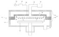
도 1과 같이, 기판처리장치(10)는 반응공간을 제공하는 공정챔버(12), 공정챔버(12) 내부의 상부에 위치하며, 플라즈마 전극으로 사용되는 후방 플레이 트(14), 후방 플레이트(14)와 연결되고 공정챔버(12)의 내부에 소스가스를 공급하는 가스 공급관(36), 후방 플레이트(14)의 하부에 위치하며, 다수의 분사홀(16)을 가지는 알루미늄 재질의 가스분배판(18), 플라즈마 전극과 대향전극으로 사용되며 기판(20)이 안치되는 기판안치대(22), 기판(20)을 공정챔버(12)로 출입 또는 반출시키기 위한 기판 출입구(40) 및 공정챔버(12)의 내부에서 사용되는 반응가스 및 부산물을 배출하기 위한 배출구(24)로 포함하여 구성된다.1, the
가스 공급관(36)은 파워 피딩 라인(power feeding line)(38)에 의해서 RF 전원(30)과 연결된다. 또한, 가스 공급관(36)은 리모트 플라즈마 콘트롤러(remote plasma controller)(50)에 연결된다. RF 전원(30)과 파워 피딩 라인(38) 사이에는 임피던스 정합을 위한 매처(matcher)(32)가 설치된다. 가스분배판(18)은 후방 플레이트(14)와 버퍼공간(26)을 가지고, 후방 플레이트(14)로부터 연장되어 연결되는 지지대(28)에 거치된다. 후방 플레이트(14)와 가스분배판(18)에 RF 전원에 인가되고, 가스분배판(18)과 기판안치대(22)의 사이에 전계에 의해 플라즈마 발생 및 되고, 소스가스가 공급되어 기판(20) 상에 박막의 증착 또는 박막의 식각이 진행된다.The
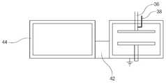
가스 공급관(36)은 공정챔버(12)의 중앙과 대응되는 후방 플레이트(14)의 중앙부에 위치한다. 후방 플레이트(14)는 가스 공급관(36)을 지나는 수직선 및 수평선을 기준으로 대칭적인 구조를 가진다. 공정챔버(12)에서 기판(20)을 처리하기 위 해서, 도 2와 같이, 기판 출입구(40)에 연결되는 슬롯밸브(slot vavle)(42) 및 기판(20)을 공정챔버(12)에 공급하거나 공정챔버(12)로부터 반출하기 위한 이송챔버(44)가 연결된다.The
공정챔버(12)에서 기판 출입구(40)의 방향으로 슬롯밸브(42) 및 이송챔버(44)가 연속적으로 설치되지만, 기판 출입구(40)와 대향하는 공정챔버(12)에는 슬롯밸브(42) 및 이송챔버(44)가 설치되지 않는다. 그리고, RF 전원(30)이 후방 플레이트(14)와 가스분배판(18)에 인가될 때, 도체로 형성된 공정챔버(12), 슬롯밸브(42) 및 이송챔버(44)의 표면을 따라 RF 전원(30)에서 공급되는 RF 전류가 흐르게된다. RF 전류는 후방 플레이트(14)와 가스 분배판(18) 외에, 인접한 도체, 즉 공정챔버(12), 슬롯밸브(42) 및 이송챔버(44)의 표면으로 전달되는 특성을 가진다.The
도 1 및 도 2와 같은 종래기술의 기판처리장치(10)에서, 플라즈마가 균일하게 발생하지 않아, 기판(20) 상에 두께가 불균일한 박막이 성막된다. 박막의 두께가 불균일한 것은 전계의 비대칭성에 기인한 것으로 추측된다. 기판 출입구(40)와 대향하는 공정챔버(12)에 흐르는 RF 전류는 단순히 공정챔버(12)의 표면을 따라 제 1 경로를 형성하지만, 기판 출입구(40)의 방향으로 슬롯밸브(40) 및 이송챔버(44)로 인해 제 1 경로 보다 매우 긴 제 2 경로를 형성한다.In the
제 1 및 제 2 경로의 차이로 인해, 전계의 비대칭성을 유발시킨다. 이러한 전계의 비대칭성은 균일한 플라즈마가 형성되는 것을 방해하여 박막의 성막에 영향을 준다. 기판 출입구(40)와 인접한 기판(20) 상에 성막되는 박막의 두께가 기판 출입구(40)와 대향하는 챔버(12)의 측벽과 인접한 기판(20) 상에 성막되는 박막의 두께보다 두껍게 형성된다. 따라서, 박막의 두께가 균일하지 못한 문제를 발생시킨다.Due to the difference in the first and second paths, it causes the asymmetry of the electric field. This asymmetry of the electric field interferes with the formation of a uniform plasma and affects the film formation of the thin film. The thickness of the thin film formed on the
상기와 같은 문제를 해결하기 위하여, 가스 분배판(18)과 기판 안치대(22) 사이의 간격을 넓게 하여, 플라즈마의 균일도를 개선할 수 있지만, 플라즈마의 밀도 저하로 인해 성막되는 박막의 밀도(density)가 저하되는 문제가 발생하였다.In order to solve the above problems, it is possible to improve the uniformity of the plasma by increasing the interval between the
상기와 같은 종래기술의 문제를 해결하기 위하여, 본 발명은 균일한 플라즈마를 발생시키기 위하여, RF 전원을 공급하는 피딩 라인을 기판의 중앙부로부터 일방향으로 이격된 지점과 대응하는 상부전극에 설치하여 균일한 두께의 박막을 성막시킬 수 있는 기판처리장치를 제공하는 것을 목적으로 한다.In order to solve the problems of the prior art as described above, in order to generate a uniform plasma, a feeding line for supplying RF power is provided on the upper electrode corresponding to a point spaced in one direction from the central portion of the substrate, And a substrate processing apparatus capable of forming a thin film having a small thickness.
상기와 같은 종래기술의 문제를 해결하기 위하여, 본 발명은 균일한 플라즈마를 발생시키기 위하여, RF 전원을 공급하는 제 1 및 제 2 피딩 라인을 구비하고, 제 1 피딩 라인은 기판의 중앙부와 대응되는 상부전극에 설치하고, 제 2 피딩 라인은 기판의 중앙부로부터 일방향으로 이격된 지점과 대응되는 상부전극에 설치하여 균일한 두께의 박막을 성막시킬 수 있는 기판처리장치를 제공하는 것을 다른 목적으로 한다.In order to solve the above problems, the present invention provides a plasma processing apparatus including first and second feeding lines for supplying RF power to generate a uniform plasma, Another object of the present invention is to provide a substrate processing apparatus capable of forming a thin film having a uniform thickness by providing a second feeding line on an upper electrode corresponding to a point spaced in one direction from a central portion of the substrate.
상기 목적을 달성하기 위한 본 발명에 따른 기판처리장치는, 반응공간을 제공하고, 제 1 측면과 상기 제 1 측면과 대향하는 제 2 측면을 가지는 챔버; 상기 제 1 측면에 연결된 모듈; 상기 반응공간에 위치하는 상부전극; 상기 상부전극과 대향하고 기판이 안치되는 기판 안치대; 상기 기판의 중앙에 위치한 제 1 지점으로부터 상기 제 1 측면의 방향으로 이격된 상기 기판의 제 2 지점과 대응되는 상기 상부전극에 연결되고 RF 전원을 인가하기 위한 피딩 라인;을 포함하는 것을 특징으로 한다.According to an aspect of the present invention, there is provided a substrate processing apparatus comprising: a chamber for providing a reaction space and having a first side and a second side opposite to the first side; A module coupled to the first side; An upper electrode positioned in the reaction space; A substrate table opposed to the upper electrode and on which the substrate is placed; And a feeding line connected to the upper electrode corresponding to a second point of the substrate spaced apart from the first point located in the center of the substrate in the direction of the first side and applying RF power thereto .
상기와 같은 기판처리장치에 있어서, 상기 제 1 측면에 상기 기판의 출입을 위한 기판 출입구가 설치되고, 상기 모듈과 상기 기판 출입구 사이에 슬롯밸브가 설치되는 것을 특징으로 한다.In the above-described substrate processing apparatus, a substrate entry / exit port for entering / exiting the substrate is provided on the first side surface, and a slot valve is provided between the module entry / exit port and the substrate.
상기와 같은 기판처리장치에 있어서, 상기 기판은 장변과 단변을 가지는 장방형이고, 상기 기판의 상기 제 1 지점과 상기 제 2 지점의 이격 간격은, 상기 기판의 장변길이에 대해 2 내지 5%인 것을 특징으로 한단.In the above substrate processing apparatus, it is preferable that the substrate is a rectangle having a long side and a short side, and a spacing distance between the first point and the second point of the substrate is 2 to 5% with respect to the long side length of the substrate Features.
상기와 같은 기판처리장치에 있어서, 상기 기판은 장변과 단변을 가지는 장방형이고, 상기 기판의 상기 제 1 지점과 상기 제 2 지점의 이격 간격은, 상기 기 판의 장변길이에 대해 2.5 내지 4%인 것을 특징으로 한다.The distance between the first point and the second point of the substrate is in the range of 2.5 to 4% with respect to the long side length of the substrate, .
상기와 같은 기판처리장치에 있어서, 상기 기판은 상기 제 2 지점을 지나는 수직선을 기준으로 비대칭이고, 상기 제 2 지점을 지나는 수평선을 기준으로 대칭인 것을 특징으로 한다.In the above substrate processing apparatus, the substrate is asymmetric with respect to a vertical line passing through the second point, and is symmetrical with respect to a horizontal line passing through the second point.
상기와 같은 기판처리장치에 있어서, 상기 제 1 지점에 대응하는 상기 상부전극에 연결되는 RF 전원을 인가하기 위한 제 2 피딩 라인을 더 포함하는 것을 특징으로 한다.The substrate processing apparatus may further include a second feeding line for applying RF power connected to the upper electrode corresponding to the first point.
상기와 같은 기판처리장치에 있어서, 상기 기판은 장변과 단변을 가지는 장방형이고, 상기 제 1 지점과 상기 제 2 지점의 이격 간격은, 상기 기판의 장변길이에 대해 10 내지 30%인 것을 특징으로 한다.In the above-described substrate processing apparatus, the substrate is a rectangular shape having a long side and a short side, and a separation distance between the first point and the second point is 10 to 30% with respect to a long side length of the substrate .
상기와 같은 기판처리장치에 있어서, 상기 기판은 장변과 단변을 가지는 장방형이고, 상기 제 1 지점과 상기 제 2 지점의 이격 간격은, 상기 기판의 장변길이에 대해 15 내지 25%인 것을 특징으로 한다.In the above-described substrate processing apparatus, the substrate may have a rectangular shape having a long side and a short side, and a spacing distance between the first point and the second point is 15 to 25% with respect to the long side length of the substrate .
상기와 같은 목적을 달성하기 위한 기판처리장치는, 반응공간을 제공하고, 제 1 측면과 상기 제 1 측면과 대향하는 제 2 측면을 가지는 챔버; 상기 반응공간에 위치하는 상부전극; 상기 상부전극과 대향하고, 장면과 단변을 가지는 장방형의 기판이 안치되는 기판 안치대; 상기 기판의 중앙에 위치한 제 1 지점으로부터 상기 제 1 측면방향으로 상기 기판의 장변길이에 대한 2 내지 5%의 간격으로 이격된 상 기 기판의 제 2 지점과 대응되는 상기 상부전극에 연결되고, RF 전원을 인가하기 위한 피딩 라인;을 포함하는 것을 특징으로 한다.According to an aspect of the present invention, there is provided a substrate processing apparatus comprising: a chamber for providing a reaction space and having a first side and a second side opposite to the first side; An upper electrode positioned in the reaction space; A substrate holder opposed to the upper electrode and having a rectangular substrate having a scene and a short side; Connected to the upper electrode corresponding to a second point of the substrate spaced apart by 2 to 5% of the length of the long side of the substrate from a first point located in the center of the substrate, And a feeding line for applying power.
상기와 같은 기판처리장치에 있어서, 상기 제 1 측면에 상기 기판의 출입을 위한 기판 출입구가 설치되고, 상기 기판 출입구에 슬롯밸브가 연결되고, 상기 슬롯밸브에 상기 반응공간으로 상기 기판을 이송하기 위한 모듈이 연결되는 것을 특징으로 한다.In the substrate processing apparatus as described above, the first side surface is provided with a substrate entry / exit port for entering / exiting the substrate, a slot valve is connected to the substrate entry / exit port, and the substrate is transferred to the reaction space And the module is connected.
상기와 같은 목적을 달성하기 위한 기판처리장치는, 반응공간을 제공하고, 제 1 측면과 상기 제 1 측면과 대향하는 제 2 측면을 가지는 챔버; 상기 반응공간에 위치하는 상부전극; 상기 상부전극과 대향하고 장변과 단변을 가지는 장방형의 기판이 안치되는 기판 안치대; 상기 기판의 중앙에 위치한 제 1 지점과, 상기 제 1 지점으로부터 상기 제 1 측면방향으로 상기 기판의 상기 장변길이에 대한 10 내지 30%의 간격으로 이격된 상기 기판의 제 2 지점에 각각 대응되는 상부전극에 연결되는 RF 전원을 인가하기 위한 제 1 및 제 2 피딩 라인;을 포함하는 것을 특징으로 한다.According to an aspect of the present invention, there is provided a substrate processing apparatus comprising: a chamber for providing a reaction space and having a first side and a second side opposite to the first side; An upper electrode positioned in the reaction space; A substrate table having a rectangular substrate facing the upper electrode and having a long side and a short side; Corresponding to a second point of the substrate spaced apart by an interval of 10 to 30% of the length of the long side of the substrate from the first point toward the first side, And first and second feeding lines for applying RF power connected to the electrodes.
상기와 같은 기판처리장치에 있어서, 상기 제 1 측면에 상기 기판의 출입을 위한 기판 출입구가 설치되고, 상기 기판 출입구에 슬롯밸브가 연결되고, 상기 슬롯밸브에 상기 반응공간으로 상기 기판을 이송하기 위한 모듈이 연결되는 것을 특 징으로 한다.In the substrate processing apparatus as described above, the first side surface is provided with a substrate entry / exit port for entering / exiting the substrate, a slot valve is connected to the substrate entry / exit port, and the substrate is transferred to the reaction space It is a feature that the module is connected.
본 발명의 기판처리장치는 다음과 같은 효과가 있다.The substrate processing apparatus of the present invention has the following effects.
피딩 라인을 기판의 중앙부에서, 이송챔버 및 슬롯밸드 등의 다른 모듈이 설치되는 기판 출입구의 방향으로 이격된 지점과 대응되는 상부전극에 연결함으로써, 기판 출입구와 대향하는 챔버의 표면으로 RF 전류가 흐르는 경로와, 기판 출입구의 방향으로 RF 전류가 흐르는 경로 사이의 전계의 대칭성을 개선하여, 균일한 플라즈마의 발생에 의해 균일한 두께의 박막을 성막할 수 있다.By connecting the feeding line to the upper electrode at the center of the substrate and corresponding to a point spaced apart in the direction of the substrate entrance where the other modules such as the transfer chamber and the slot-bed are installed, RF current flows to the surface of the chamber facing the substrate entrance It is possible to improve the symmetry of the electric field between the path and the path through which the RF current flows in the direction of the substrate entrance and to form a thin film of uniform thickness by the generation of uniform plasma.
RF 전원을 공급하는 제 1 및 제 2 피딩 라인을 구비하고, 제 1 피딩 라인을 기판의 중앙부와 대응되는 상부전극에 연결하고, 제 2 피딩 라인을 기판의 중앙부로부터 이송챔버 및 슬롯밸드 등의 다른 모듈이 설치되는 기판 출입구의 방향으로 이격된 지점과 대응되는 상부전극에 연결함으로써, 기판 출입구와 대향하는 챔버의 표면으로 RF 전류가 흐르는 경로와, 기판 출입구의 방향으로 RF 전류가 흐르는 경로 사이의 전계의 비대칭성을 개선하여, 균일한 플라즈마의 발생에 의해 균일한 두께의 박막을 성막할 수 있다.The first feeding line is connected to the upper electrode corresponding to the central portion of the substrate, and the second feeding line is connected to the feeding chamber and the other of the feeding chamber and the slot- And an upper electrode corresponding to a point spaced apart from the substrate in the direction of the substrate entry port on which the module is installed so that an electric field between the path through which the RF current flows to the surface of the chamber facing the substrate entrance and the path through which the RF current flows in the direction of the substrate entrance, It is possible to form a thin film having a uniform thickness by the generation of a uniform plasma.
이하에서는 도면을 참조하여 본 발명의 바람직한 실시예를 상세히 설명하기로 한다.Hereinafter, preferred embodiments of the present invention will be described in detail with reference to the drawings.
도 3은 본 발명의 제 1 실시예에 따른 기판처리장치의 개략도이고, 도 4는 본 발명의 제 1 실시예에 따른 이송장치를 포함한 기판처리장치의 모식도이고, 도 5는 본 발명의 제 1 실시예에 따른 기판처리장치의 평면도이고, 도 8은 본 발명의 제 1 실시예에 따른 파워 피딩 라인의 이격 비율에 따른 박막 두께를 도시한 그래프이고, 도 9는 본 발명의 제 1 실시예에 따른 파워 피딩 라인의 이격 비율에 따른 박막 균일도를 도시한 그래프이다.FIG. 3 is a schematic view of a substrate processing apparatus according to a first embodiment of the present invention, FIG. 4 is a schematic diagram of a substrate processing apparatus including a transfer apparatus according to the first embodiment of the present invention, and FIG. FIG. 8 is a graph showing a thickness of a thin film according to a separation ratio of a power feeding line according to the first embodiment of the present invention, and FIG. 9 is a graph showing the thickness of thin film according to the first embodiment of the present invention And FIG. 5 is a graph showing the uniformity of the thin film according to the separation ratio of the power feeding line according to the embodiment of the present invention.
도 3과 같이, 반도체 또는 대면적의 액정표시장치에서 사용되는 기판을 처리하는 기판처리장치(110)는 반응공간을 제공하고 제 1 측면과 제 1 측면과 대향하는 제 2 측면을 가지는 공정챔버(112), 공정챔버(112) 내부의 상부에 위치하며, 상부전극으로 사용되는 후방 플레이트(114), 후방 플레이트(114)와 연결되고 공정챔버(112)의 내부에 소스가스를 공급하는 가스 공급관(136), 후방 플레이트(114)의 하부에 위치하며, 다수의 분사홀(116)을 가지는 알루미늄 재질의 가스분배판(118), 플라즈마 전극과 대향전극으로 사용되며 기판(120)이 안치되는 기판안치대(122), 기판(120)을 반입 또는 반출시키기 위해 제 1 측면에 설치되는 기판 출입구(140), 및 공정챔버(112)의 내부에서 사용되는 반응가스 및 부산물을 배출하기 위한 배출구(124)로 포함하여 구성된다.As shown in FIG. 3, a
공정챔버(112)에서 기판(120)을 처리하기 위해서, 도 4와 같이, 기판 출입구(140)에 슬롯밸브(slot vavle)(142)가 연결되고, 슬롯밸브(142)에 기판(120)을 공정챔버(112)에 공급하거나 공정챔버(112)로부터 기판(120)을 반출하기 위한 모듈(144)이 연결된다. 모듈(144)은 이송챔버 또는 로드락 챔버를 포함할 수 있다. 공정챔버(112)에 이송챔버(144)를 연결하는 경우, 기판 출입구(140)의 방향으로 슬롯밸브(142) 및 이송챔버(144)가 연속적으로 설치되지만, 기판 출입구(140)가 설치된 공정챔버(112)의 제 1 측면과 대향하는 공정챔버(112)의 제 2 측면에는 슬롯밸브(142) 및 모듈(144)이 설치되지 않는다.In order to process the
공정챔버(112)는 챔버몸체(112a)와, 챔버몸체(112a)에 착탈 가능하도록 결합되어 반응공간을 밀봉시키는 챔버리드(112b)를 포함한다. 챔버몸체(112a)는 상부가 개방된 원통형 또는 장방형의 사각형을 포함하는 다각형의 형태로 제작되고, 챔버리드(112b)는 챔버몸체(112a)와 대응되는 형태를 가지는 플레이트(plate) 형상으로 제작된다. 도면에서 도시하지 않았지만, 챔버리드(112a)와 챔버몸체(112b)는 밀봉부재, 예를 들면 오링(O-ring) 또는 가스켓을 개재하고, 고정부재를 사용하여 결합시킨다.The
가스 공급관(136)은 리모트 플라즈마 콘트롤러(remote plasma controller)(150)에 연결된다. RF 전원(130)과 파워 피딩 라인(138) 사이에는 임피 던스 정합을 위한 매처(matcher)(132)가 설치된다. 가스분배판(118)와 후방 플레이트(114)의 사이에 버퍼공간(126)이 형성되고, 가스분배판(118)은 후방 플레이트(114)로부터 연장되어 연결되는 지지대(128)에 거치된다.The
버퍼공간(126)은 가스 공급관(136)으로부터 공급되는 소스가스를 수용하고, 후방 플레이트(114)는 버퍼공간(126)의 상부로 소스가스가 외부로 누출되는 것을 방지한다. 따라서, 소스가스는 가스분배판(118)을 통하여 기판안치대(122)의 방향으로 균일하게 분사된다. 후방 플레이트(114)와 가스분배판(118)에 RF 전원에 인가되고, 가스분배판(118)과 기판안치대(122)의 사이에 전계에 의해 플라즈마가 발생되고, 소스가스가 공급되어 기판(120) 상에 박막증착 또는 식각이 진행된다.The
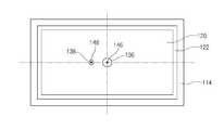
도 5와 같이, 기판 안치대(122) 상에 기판(120)이 위치하고, 기판(120)의 중앙에 위치한 제 1 지점(146)과 대응하는 후방 플레이트(114)에 가스 공급관(136)이 연결된다. 기판(120)은 가스 공급관(136)과 대응하는 제 1 지점(146)을 지나는 수직선 및 수평선을 기준으로 각각 대칭적인 구조를 가진다. 가스 공급관(136)은 후방 플레이트(114)의 중앙부에 위치할 수 있고, 후방 플레이트(114)는 가스 공급관(136)을 지나는 수직선 및 수평선을 기준으로 각각 대칭적인 구조를 가질 수 있다.5, the
RF 전원(130)과 연결되는 파워 피딩 라인(138)은 기판(120)의 중앙부에 위치 하고 가스 공급관(136)과 대응되는 제 1 지점(146)으로부터, 기판 출입구(140)가 설치되는 공정챔버(112)의 제 1 측면의 방향으로 기판(120)의 장변길이의 2 내지 5% 정도의 간격으로 이격되는 제 2 지점(148)과 대응되는 후방 플레이트(114)에 연결된다. 파워 피딩 라인(138)은 가스 공급관(136)과 대응되는 기판(114)의 제 1 지점(146)으로부터 기판(114)의 장변길이의 3 내지 4% 정도의 간격으로 이격되는 제 2 지점(148)과 대응되는 후방 플레이트(114)에 설치되는 것이 바람직하다.The
그리고, 기판(120) 상에 성막되는 박막 균일도를 4% 이내로 유지하기 위해서, 파워 피딩 라인(138)은 가스 공급관(136)과 대응되는 기판(114)의 제 1 지점(146)으로부터 기판(114)의 장변길이의 2.5 내지 4% 정도의 간격으로 이격되는 제 2 지점(148)과 대응되는 후방 플레이트(114)에 설치되는 것이 바람직하다. 기판(120)은 파워 피딩 라인(138)과 대응되는 제 2 지점(148)을 지나는 수직선을 기준으로 비대칭이고, 제 2 지점(148)을 지나는 수평선을 기준으로 대칭이다. 도 3 및 도 5에서는 하나의 파워 피딩 라인(138) 만이 제 2 지점(148)에 대응되는 후방 플레이트(114)에 연결되는 것으로 한정할 수 있다.The
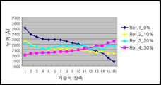
도 8 및 도 9는 본 발명의 제 1 실시예에서, 기판(120)의 중앙에 위치한 제 1 지점(146)과 대응되는 가스공급관(136)과 기판 출입구(140)의 방향으로 제 1 지점(146)으로부터 이격된 제 2 지점(148)과 대응되는 후방 플레이트(114)에 연결되는 파워 피딩라인(138)의 간격 변화에 따른 박막 두께와 박막 균일도를 도시한 그 래프이다.8 and 9 illustrate a
도 8에서, Y 축은 박막의 두께(Å)를 나타내고, X 축은 기판(120)의 제 1 지점(146)을 지나는 장축을 의미한다. 박막 두께는 기판(120)의 제 1 지점(146)을 지나는 수평선에 일정간격으로 이격된 다수의 측정위치를 정의하고, 기판(120)의 제 1 지점(146)과 제 2 지점(148)과 각각 대응되고 후방 플레이트(114)에 설치되는 가스 공급관(136)과 파워 피딩 라인(138)의 이격 간격에 따라 다수의 측정위치에서 박막 두께를 측정한다. 도 9에서, Y축은 박막 균일도를 나타내고, X축은 기판(120)의 중앙에 위치한 제 1 지점(146)과, 대응되는 가스공급관(136)과 기판 출입구(140)의 방향으로 제 1 지점(146)으로부터 이격된 제 2 지점(148)과 대응되는 후방 플레이트(114)에 연결되는 파워 피딩라인(138)의 간격 변화에 대한 비율을 나타낸다.In FIG. 8, the Y axis represents the thickness (A) of the thin film, and the X axis represents the long axis passing through the
기판(120) 상에 여러가지 종류 또는 기능을 가지는 물질로 구성되는 박막을 증착할 수 있지만, 본 발명의 제 1 실시예에서는, 액정표시소자의 공정에서 대표적으로 사용하는 실리콘 질화막을 성막한다. 실리콘 질화막의 증착조건은 공정가스로 SiH4, NH3 및 N2가스를 각각 6500 sccm, 28000 sccm 및 76500 sccm의 유량으로 공급하고, 공정챔버(112)의 압력 및 온도는 1.2torr 및 290 내지 295℃를 유지하고, 그리고, 파워 피딩라인(138)에는 RF 파워(power)로 22 KW을 인가한다. 또한, 기 판(120)은 액정표시소자에서 사용하는 장변, 단면 및 두께가 각각 2500mm, 2200mm 및 0.7mm을 가지는 유리기판을 사용한다.A thin film made of a material having various kinds or functions can be deposited on the
본 발명은 액정표시장치의 8세대 장비에서 사용되는 기판(120)을 사용하여 박막의 두께를 측정한다. 기판(120)은 장변과 단변이 각각 250cm 및 220cm의 길이를 가지는 장방형이다. 도 3 내지 도 5의 본 발명의 제 1 실시예에서, 기판(120)의 장변 및 단변이 각각 250cm 및 220cm의 길이를 가진 경우, 가스 공급관(136)과 파워 피딩 라인(138)과 각각 대응되는 기판(120)의 제 1 지점(146) 및 제 2 지점(148)의 간격은, 기판(120)의 장변길이의 비율에 따라 표 1과 같이 정의된다.The present invention measures the thickness of a thin film using a
표 1Table 1
기판(120)의 제 1 지점(146)을 지나는 장축에 균일한 간격을 가지는 다수의 측정위치를 정의하고, 표 1의 Ref.1 내지 Ref.5에 의해서 성막되는 박막의 두께를 측정하여, 최대치과 최소치에 의해 박막 균일도를 계산하면 표 2와 같다. 도 9는 표 2를 그래프로 도시한 것이다.A plurality of measurement positions having uniform intervals on the long axis passing through the
표 2Table 2
표 1에서, Ref.1의 경우, 파워 피딩 라인(138)은 가스 공급관(136)에 연결되어, 실제로 제 1 지점(146)과 제 2 지점(148)의 간격이 0cm인 경우이고, Ref.2 내지 Ref. 5는 기판(120)의 장변길이에 대하여 각각 2 내지 5%의 비율로 제 2 지점(148)이 제 1 지점(146)으로부터 이격된 경우이다. 표 2에서, 박막 균일도는 "(최대치-최소치)/(최대치+최소치)*100"의 수식에 의해 계산된다.In Table 1, in Ref.1, the
표 1의 Ref.1과 같이, 파워 피딩 라인(138)이 가스 공급관(136)에 연결되어, 실질적으로 파워 피딩 라인(138)이 기판(120)의 중앙과 대응되는 후방 플레이트(114)에 위치한 경우, 기판 출입구(140)가 설치되는 제 1 측면과 인접한 기판(120) 상에 성막되는 박막의 두께(대략적으로 2,500Å)가 기판 출입구(140)와 대향하는 공정챔버(112)의 제 2 측면과 인접한 기판(120) 상에 성막되는 박막의 두께(대략적으로 1,900Å)보다 매우 두껍게 형성된다. 따라서, 표 1의 Ref. 1의 경우, 기판(120) 상에 형성되는 박막 균일도는, 표 2와 같이, 14.40%에 달하여 박막 두께의 편차가 매우 극심함을 알 수 있다.The
그러나, 표 1의 Ref.2 내지 Ref.5와 같이, 기판(120)의 제 1 지점(146)으로부터 이격된 제 2 지점(148)과 대응되는 후방 플레이트(114)에 파워 피딩 라인(138)을 연결시키는 경우, 기판(120) 상에 적층되는 박막 균일도가 표 2와 같이 현저하게 개선되는 것을 알 수 있다.However, as shown in Ref.2 to Ref.5 of Table 1, a
표 1과 같이, 제 2 지점(148)을 제 1 지점(146)으로부터 5cm 이격시킨 Ref.2의 경우, 박막의 두께는 기판 출입구(140)가 설치되는 제 1 측면과, 제 1 측면과 대향하는 공정챔버(112)의 제 2 측면과 대응하는 기판(120) 상에 두껍고 형성되고, 기판(120)의 중앙부에서 얇게 되는 현상이 발생하지만, 대체적으로 표 2를 통해 볼 수 있는 것 처럼, Ref.1 보다는 개선된 6.13%의 박막 균일도를 나타낸다.As shown in Table 1, in the case of Ref.2 in which the
표 1과 같이, 제 2 지점(148)을 제 1 지점(146)으로부터 12.5cm 이격시킨 Ref.5의 경우, 박막의 두께는 공정챔버(112)의 제 1 측면에서 중앙부의 방향으로 일시적으로 감소하다가 제 1 측면과 대향하는 공정챔버(112)의 제 2 측면방향으로 점진적으로 증가하는 형태로, 표 2와 같이, Ref.1 보다 개선된 5.58%의 박막 균일도를 보여준다. 표 1과 같이, Ref.3 및 Ref.4의 경우, 박막의 두께는 공정챔버(112)의 제 1 측면과 제 1 측면과 대향하는 공정챔버(112)의 제 2 측면과 대응되는 분에서 약간의 편차를 보이지만, 각각 상대적으로 균일한 2.15% 및 3.67%의 박막 균일도를 나타낸다.For Ref. 5 where the
그리고, 도 8과 같이, 기판 출입구(140)의 방향으로 제 1 지점(146)과 파워 피딩 라인(138)과 대응되는 제 2 지점(148)의 간격이 기판(120)의 장변길이에 대하여 3 내지 5 %의 범위에 있는 Ref. 3 내지 Ref. 5에서는, Ref.1 및 Ref.2와 비교하여, 공정챔버(112)의 제 1 측면과 인접한 기판(120) 상에 성막되는 박막의 두께가 공정챔버(112)의 제 1 측면과 대향하는 공정챔버(112)의 제 2 측면과 인접한 기판(120) 상에 성막되는 박막의 두께보다 얇게 형성되는 역전현상이 나타난다.8, the distance between the
도 8, 도 9, 표 1 및 표 2와 같은 실험결과에 따라, 파워 피딩 라인(138)은 기판(120)의 제 1 지점(146)으로부터 대략적으로 5 내지 12cm 정도 이격되는 제 2 지점(148)과 대응되는 후방 플레이트(114)에 연결하면 박막 균일도를 10% 이내로 개선할 수 있다. 표 1의 Ref. 2 내지 Ref. 5의 조건으로 박막을 증착하는 경우, 표 2와 박막 균일도가 0 내지 10% 이내의 범위에 위치한다.According to the experimental results shown in FIGS. 8, 9, and 1 and 2, the
파워 피딩 라인(138)은 바람직하게 제 1 지점(146)으로부터 7 내지 10cm 정도 이격된 제 2 지점(148)과 대응되는 후방 플레이트(114)에 연결하면, 더욱 박막의 균일도를 개선할 수 있다. 박막 균일도는 극단적으로 0%일 경우가 가장 바람직하고, 낮으면 낮을수록 좋다. 일반적으로, 표시장치 및 반도체 소자에 적용되는 경우, 박막의 균일도는 10% 이내가 용인되는 범위이지만, 고도의 정밀성이 요구되는 박막의 경우에, 박막 균일도는 더욱 0%에 가까워지는 조건을 선택할 수 있다.The
양질의 제품을 제조하기 위하여, 기판(120) 상에 성막되는 박막은, 4% 이내의 박막 균일도를 유지하는 것이 바람직하다. 도 9를 참조하면, 0 내지 4%의 박막 균일도와 대응되는 파워 피딩 라인(138)이 이격비율은 기판(114)의 장변길이의 A 범위, 즉 2.5 내지 4%인 것을 알 수 있다. 따라서, 기판(120) 상에 성막되는 박막 균일도의 범위가 0 내지 4% 이내로 유지하기 위해서, 파워 피딩 라인(138)은 가스 공급관(136)과 대응되는 기판(114)의 제 1 지점(146)으로부터 기판(114)의 장변길이의 2.5 내지 4% 정도의 간격으로 이격되는 제 2 지점(148)과 대응되는 후방 플레이트(114)에 설치되는 것이 바람직하다.In order to produce a good quality product, it is desirable that the thin film to be formed on the
기판 출입구(140)의 방향으로 기판(120)의 장변길이에 대하여, 제 1 지점(146)으로부터 2 내지 5 %의 범위로 이격시킨 제 2 지점(148)에 파워 피딩 라인(138)을 설치하는 것은 수많은 실험의 결과치를 분석하여 얻은 결과이다. 그리고, 파워 피딩 라인(138)의 위치에 따라 전계의 중심이 이동되기 때문에, 성막되는 박막의 두께가 변화하는 것으로 분석된다.A
RF 전원(130)에 의해서 후방 플레이트(114)와 가스분배판(118)에 인가되는 것과 함께, 도체로 형성된 공정챔버(112), 슬롯밸브(142) 및 모듈(144)의 표면을 따라 RF 전원(130)에 의한 RF 전류가 흐르게 된다. RF 전류는 후방 플레이트(114)와 가스 분배판(118) 외에, 인접한 도체, 즉 공정챔버(112), 슬롯밸브(142) 및 모듈(144)의 표면으로 전달되는 특성을 가진다.Along with the surface of
도 3 내지 도 5와 같이, 파워 피딩 라인(138)을 설치하면, 기판(120) 상에 성막되는 박막 균일도가 개선된다. 종래기술의 RF 전계의 비대칭성을 개선하였기 때문에, 본 발명의 제 1 실시예에서, 균일한 박막의 형성되는 것으로 분석된다. 파워 피딩 라인(138)으로부터 기판 출입구(140)와 대향하는 공정챔버(112)의 표면을 따라 흐르고 접지되는 RF 전류는 제 1 경로를 형성하고, 파워 피딩 라인(138)으로부터 기판 출입구(140)의 방향으로는 공정챔버(112), 슬롯밸브(140) 및 모듈(144)의 표면을 따라 흐르고 접지되는 RF 전류는 제 2 경로를 형성한다. 공정챔버(112)의 중앙으로부터 기판 출입구(140)으로 방향으로 이동시켜 파워 피딩 라인(138)을 설치하는 것에 의해, 제 1 및 제 2 경로를 따라 흐르는 RF 전류의 비대칭성을 개선하여, 기판(120) 상에 박막 두께의 편차가 최소화된다.As shown in FIGS. 3 to 5, when the
상기와 같은 파워 피딩 라인(138)을 중앙으로부터 이동하여 설치하는 것에 의해, 실질적으로 제 1 및 제 2 경로를 따라 흐르는 RF 전류가 실질적으로 대칭되는 효과를 가질 수 있다. 또한, 가스 공급관(136)을 파워 피딩 라인(138)이 설치되는 지점의 후방 플레이트(114)에 설치하고, 가스 공급관(136)에 파워 피딩 라인(138)을 연결할 수 있다.By moving and installing the
도 6은 본 발명의 제 2 실시예에 따른 기판처리장치의 개략도이고, 도 7은 본 발명의 제 2 실시예에 따른 기판처리장치의 평면도이고, 도 10은 본 발명의 제 2 실시예에 따른 파워 피딩 라인의 이격 비율에 따른 박막 두께를 도시한 그래프이고, 도 11은 본 발명의 제 2 실시예에 따른 파워 피딩 라인의 이격 비율에 따른 박막 균일도를 도시한 그래프이다.FIG. 6 is a schematic view of a substrate processing apparatus according to a second embodiment of the present invention, FIG. 7 is a plan view of a substrate processing apparatus according to a second embodiment of the present invention, FIG. 10 is a cross- FIG. 11 is a graph showing a uniformity of a thin film according to a separation ratio of a power feeding line according to a second embodiment of the present invention. FIG.
도 6 및 도 7과 같이, 기판 안치대(122) 상에 기판(120)이 위치하고, 기판(120)의 중앙에 위치한 제 1 지점(146)과 대응하는 후방 플레이트(114)에 가스 공급관(136)이 연결된다. 기판(120)은 가스 공급관(136)과 대응하는 제 1 지점(146)을 지나는 수직선 및 수평선을 기준으로 각각 대칭적인 구조를 가진다. 가스 공급관(136)은 후방 플레이트(114)의 중앙부에 위치할 수 있고, 후방 플레이트(114)는 가스 공급관(136)을 지나는 수직선 및 수평선을 기준으로 각각 대칭적인 구조를 가질 수 있다.6 and 7, a
RF 전원(130)과 연결되는 파워 피딩 라인(138)은 제 1 및 제 2 파워 피딩 라인(138a, 138b)으로 구성된다. 제 1 파워 피딩 라인(138a)은 가스 공급관(136)에 연결되고, 제 2 파워 피딩 라인(138b)은 기판 출입구(140)의 방향으로 가스 공급관(136)과 대응되는 기판(120)의 제 1 지점(146)으로부터, 기판(120)의 장변길이의 10 내지 30% 정도의 간격으로 이격되는 제 2 지점(148)과 대응되는 후방 플레이트(114)에 연결된다. 제 2 파워 피딩 라인(138b)은 기판 출입구(140)의 방향으로 가스 공급관(136)과 대응되는 기판(120)의 제 1 지점(146)으로부터 기판(120)의 장변길이의 20% 정도의 간격으로 이격되는 제 2 지점(148)과 대응되는 후방 플레이 트(114)에 연결하는 것이 바람직하다.The
기판(120)은 제 2 파워 피딩 라인(138b)과 대응되는 제 2 지점(148)를 지나는 수직선을 기준으로 비대칭이고, 제 2 지점(148)을 지나는 수평선을 기준으로 대칭이다. 필요에 따라, 2 개 이상의 파워 피딩 라인(138)을 설치할 수 있다. 2 개 이상의 파워 피딩 라인(138)을 설치하는 경우, 기판(120)의 제 1 지점(146)과 대응되는 후방 플레이트(114)에 설치되는 파워 피딩 라인(138)을 제외하고, 다른 파워 피딩 라인(138)은 기판 출입구(140)와 기판(120)의 제 1 지점(146) 사이와 대응되는 후방 플레이트(114)에 설치된다.The
가스 공급관(136)이 후방 플레이트(114)의 중앙부에 위치하는 경우, 제 1 파워 피딩 라인(138a)는 가스 공급관(136)에 연결되고, 제 2 파워 피딩 라인(138b)은 후방 플레이트(114)의 장변길이의 10 내지 30% 정도의 간격으로 이격된 지점의 후방 플레이트(114)에 연결될 수 있다. 바람직하게, 제 2 파워 피딩 라인(138b)은 가스 공급관(136)의 중심으로부터 후방 플레이트(114)의 장변길이의 10% 정도의 간격으로 이격되는 지점의 후방 플레이트(114)에 설치된다.The first
기판(120) 상에 성막되는 박막 균일도의 범위가 0 내지 4% 이내로 유지하기 위해서 가스 공급관(136)에 연결되는 제 1 파워 피딩 라인(138a)과 제2 파워 피딩 라인(138b)과 각각 대응되는 기판(120)의 제 1 지점(146) 및 제 2 지점(148)은 기 판(114)의 장변길이의 15 내지 25% 정도의 간격으로 이격되는 것이 바람직하다. 제 2 파워 피딩 라인(138b)을 지나는 수직선을 기준으로 후방 플레이트(114)는 비대칭이고, 제 2 파워 피딩 라인(138b)을 지나는 수평선을 기준으로 후방 플레이트(114)는 대칭이다. 도 6 및 도 7에서는 두 개의 파워 피딩 라인(138a, 138b) 만이 제 1 지점(146) 및 제 2 지점(148)에 대응되는 후방 플레이트(114)에 연결되는 것으로 한정할 수 있다.The first
도 10 및 도 11은 본 발명의 제 2 실시예에서, 기판(120)의 중앙에 위치한 제 1 지점(146)과 대응되는 가스공급관(136)에 제 1 파워 피딩 라인(138a)을 연결하고, 제 1 지점(146)으로부터 기판 출입구(140)의 방향으로 이격된 제 2 지점(148)과 대응되는 후방 플레이트(114)에 제 2 파워 피딩 라인(138b)을 연결하는 경우, 제 1 지점(146)과 제 2 지점(148)의 간격변화에 따른 박막 두께와 박막 균일도를 도시한 그래프이다.10 and 11 show a second embodiment of the present invention in which a first
도 10에서, Y 축은 박막의 두께(Å)를 나타내고, X 축은 기판(120)의 제 1 지점(146)을 지나는 장축을 의미한다. 박막 두께는 기판(120)의 제 1 지점(146)을 지나는 수평선에 일정간격으로 이격된 다수의 측정위치를 정의하고, 제 1 파워 피딩 라인(138a) 및 제 2 파워 피딩 라인(138b)과 각각 대응되는 기판(120)의 제 1 및 제 2 지점(146, 148)의 이격 간격에 따라 다수의 측정위치에서 박막 두께를 측정한다. 도 11에서, Y축은 박막 균일도를 나타내고, X축은 기판(120)의 중앙에 위 치한 제 1 지점(146)과, 대응되는 가스공급관(136)과 기판 출입구(140)의 방향으로 제 1 지점(146)으로부터 이격된 제 2 지점(148)과 대응되는 후방 플레이트(114)에 각각 연결되는 제 1 및 제 2 파워 피딩라인(138a, 138b)의 간격 변화에 대한 비율을 나타낸다.10, the Y axis represents the thickness (Å) of the thin film, and the X axis represents the long axis passing through the
기판(120) 상에 여러가지 종류 또는 기능을 가지는 물질로 구성되는 박막을 증착할 수 있지만, 본 발명의 제 2 실시예에서는, 액정표시소자의 공정에서 대표적으로 사용하는 실리콘 질화막을 증착한다. 실리콘 질화막의 증착조건은 공정가스로 SiH4, NH3 및 N2가스를 각각 6500 sccm, 28000 sccm 및 76500 sccm의 유량으로 공급하고, 공정챔버(112)의 압력 및 온도는 1.2torr 및 290 내지 295℃를 유지하고, 그리고, 파워 피딩라인(138)에는 RF 파워(power)로 22 KW을 인가한다. 또한, 기판(120)은 액정표시소자에서 사용하는 장변, 단면 및 두께가 각각 2500mm, 2200mm 및 0.7mm을 가지는 유리기판을 사용한다.A thin film made of a material having various kinds or functions can be deposited on the
본 발명은 액정표시장치의 8세대 장비에서 사용되는 기판(120)을 사용하여 박막의 균일도를 측정한다. 기판(120)은 장변과 단변이 각각 250cm 및 220cm의 길이를 가지는 장방형이다. 도 6 및 도 7의 본 발명의 제 2 실시예에서, 기판(120)의 장변 및 단변이 각각 250cm 및 220cm의 길이를 가진 경우, 가스 공급관(136)에 연결되는 제 1 파워 피딩 라인(138a)과 제2 파워 피딩 라인(138b)과 각각 대응되는 기판(120)의 제 1 지점(146) 및 제 2 지점(148)의 이격 간격은, 기판(120)의 장변길이의 비율에 따라 표 3과 같이 정의된다.The present invention measures the uniformity of a thin film using a
표 3Table 3
기판(120)의 제 1 지점(146) 및 제 2 지점(148)을 지나는 장축에 균일한 간격을 가지는 다수의 측정위치를 정의하고, 표 3의 Ref.1 내지 Ref.4에 의해서 성막되는 박막의 두께를 측정하여, 최대치과 최소치에 의해 박막 균일도를 계산하면 표 4와 같다. 도 11은 표 4를 그래프로 도시한 것이다.A plurality of measurement positions having a uniform interval on a long axis passing through the
표 4Table 4
표 3에서, Ref.1의 경우, 제 1 및 제 2 파워 피딩 라인(138a, 138b)은 모두 가스 공급관(136)에 연결되어, 실제로 제 1 지점(146)과 제 2 지점(148)의 간격이 0cm인 경우이고, Ref.2 내지 Ref. 4는 기판(120)의 장변길이에 대하여 각각 10 내지 30%의 비율로 제 2 지점(148)이 제 1 지점(146)으로부터 이격된 경우이다. 표 4 에서, 박막 균일도는 "(최대치-최소치)/(최대치+최소치)*100"의 수식에 의해 계산된다.In Table 3, in Ref.1, both the first and second
표 3의 Ref.1과 같이, 제 1 및 제 2 파워 피딩 라인(138a, 138b)이 모두 가스 공급관(136)에 연결되어, 실질적으로 제 2 파워 피딩 라인(138b)이 기판(120)의 중앙에 위치한 경우, 기판 출입구(140)가 설치되는 공정챔버(112)의 제 1 측면과 인접한 기판(120) 상에 성막되는 박막의 두께(대략적으로 2,500Å)가 공정챔버(112)의 제 1 측면과 대향하는 공정챔버(112)의 제 2 측면과 인접한 기판(120) 상에 성막되는 박막의 두께(대략적으로 1,900Å)보다 매우 두껍게 형성된다. 따라서, 표 3의 Ref. 1의 경우, 기판(120) 상에 형성되는 박막 균일도는 표 2와 같이 14.14%에 달하여 박막 두께의 편차가 매우 극심함을 알 수 있다.The first and second
그러나, 표 3의 Ref.2 내지 Ref.4와 같이, 제 1 파워 피딩 라인(138a)은 기판(120)의 중앙에 위치한 제 1 지점(146)과 대응되는 가스 공급관(136)에 연결되고, 제 2 파워 피딩 라인(138b)은 기판(120)의 제 1 지점(146)으로부터 이격된 제 2 지점(148)과 대응되는 후방 플레이트(114)에 연결된 경우, 기판(120) 상에 적층되는 박막 균일도는 표 4와 같이, 현저하게 개선되는 것을 알 수 있다.However, as shown in Ref.2 to Ref.4 of Table 3, the first
제 2 지점(148)을 제 1 지점(146)으로부터 25cm 이격시킨 표 3의 Ref.2의 경우, 박막의 두께는 기판 출입구(140)가 설치된 공정챔버(112)의 제 1 측면과 인접 한 부분이 공정챔버(112)의 제 1 측면과 대향하는 공정챔버(112)의 제 2 측면과 대응하는 부분보다 두껍고 형성되지만, 대체적으로 표 3의 Ref.1 보다는 개선된 5.46%의 박막 균일도를 보여준다. 제 2 지점(148)을 제 1 지점(146)으로부터 50cm 이격시킨 표 3의 Ref.3의 경우, 박막의 두께는 기판 출입구(140)가 설치되는 공정챔버(112)의 제 1 측면과 인접한 부분이 공정챔버(112)의 제 1 측면과 대향하는 공정챔버(112)의 제 2 측면과 대응하는 부분보다 두껍게 형성되지만. Ref.1 및 Ref. 2보다 개선된 2.36%의 박막 균일도를 보여준다. Ref.4의 경우, 박막의 두께는 공정챔버(112)의 제 1 측면에서 제 2 측면방향까지 까지 증가하는 형태를 보이지만, Ref.1 보다는 개선된 5.87%의 박막 균일도를 보여준다.In Ref.2 of Table 3, where the
도 10, 도 11, 표 3 및 표 4와 같은 실험결과에 따라, 기판(120)의 제 1 지점(146) 및 제 2 지점(148)과 각각 대응되는 제 1 및 제 2 파워 피딩 라인(138a, 138b)의 이격 간격이 대략적으로 25 내지 75cm 정도인 경우 박막 균일도를 10% 이내로 개선할 수 있다. 표 3의 Ref. 2 내지 Ref. 4의 조건으로 박막을 증착하는 경우, 표 4와 박막 균일도가 0 내지 10% 이내의 범위에 위치한다. 제 2 파워 피딩 라인(138b)은 바람직하게 제 1 지점(146)과 대응되는 제 1 파워 피딩 라인(138a)으로부터 50cm 정도 이격된 제 2 지점(148)과 대응되는 후방 플레이트(114)에 연결하면, 더욱 박막의 균일도를 개선할 수 있다.The first and second
도 6 내지 도 7과 같은 본 발명의 제 2 실시예에서, 후방 플레이트(114)의 장변 및 단변이 각각 250cm 및 220cm의 길이를 가진다면, 제 2 파워 피딩 라인(138b)이 설치되는 지점은, 중앙부로부터 대략적으로 25 내지 75cm 정도 이격된 지점에 설치하고, 바람직하게는 50cm 정도 이격된 지점에 설치한다. 실질적으로 RF 전원은 제 1 및 제 2 파워 피딩 라인(138a, 138b)의 중간지점에서 인가되는 것과 동일한 효과를 가진다.In the second embodiment of the present invention as shown in Figs. 6 to 7, if the long side and the short side of the
박막 균일도는 극단적으로 0%일 경우가 가장 바람직하고, 낮으면 낮을수록 좋다. 일반적으로, 표시장치 및 반도체 소자에 적용되는 경우, 박막의 균일도는 10% 이내가 용인되는 범위이지만, 고도의 정밀성이 요구되는 박막의 경우에, 박막 균일도는 더욱 0%에 가까워지는 조건을 선택할 수 있다.The film uniformity is most preferably 0%, and the lower the better, the better. Generally, when applied to a display device and a semiconductor device, the uniformity of the thin film is within 10%, but in the case of a thin film requiring high precision, a condition that the film uniformity becomes closer to 0% can be selected have.
양질의 제품을 제조하기 위하여, 기판(120) 상에 성막되는 박막은, 4% 이내의 박막 균일도를 유지하는 것이 바람직하다. 도 11을 참조하면, 0 내지 4%의 박막 균일도와 대응되는 제 1 및 제 2 파워 피딩 라인(138a, 138b)이 이격거리는 기판(114)의 장변길이의 B 범위, 즉 15 내지 25%인 것을 알 수 있다. 따라서, 기판(120) 상에 성막되는 박막 균일도의 범위가 0 내지 4% 이내로 유지하기 위해서 가스 공급관(136)에 연결되는 제 1 파워 피딩 라인(138a)과 제2 파워 피딩 라인(138b)과 각각 대응되는 기판(120)의 제 1 지점(146) 및 제 2 지점(148)은 기판(114)의 장변길이의 15 내지 25% 정도의 간격으로 이격되는 것이 바람직하다.In order to produce a good quality product, it is desirable that the thin film to be formed on the
기판 출입구(140)의 방향으로 기판(120)의 장변길이에 대하여, 제 1 지점(146)으로부터 10 내지 30%의 범위로 이격시킨 제 2 지점(148)에 제 2 파워 피딩 라인(138b)을 설치하는 것은 수많은 실험의 결과치를 분석하여 얻은 결과이다. 그리고, 제 2 파워 피딩 라인(138b)의 위치에 따라 전계의 중심이 이동되기 때문에, 성막되는 박막의 두께가 변화하는 것으로 분석된다.A second
RF 전원(130)에 의해서 후방 플레이트(114)와 가스분배판(118)에 인가되는 것과 함께, 도체로 형성된 공정챔버(112), 슬롯밸브(142) 및 이송챔버(144)의 표면을 따라 RF 전원(130)에 의한 RF 전류가 흐르게 된다. RF 전류는 후방 플레이트(114)와 가스 분배판(118) 외에, 인접한 도체, 즉 공정챔버(112), 슬롯밸브(142) 및 이송챔버(144)의 표면으로 전달되는 특성을 가진다.Along the surface of the
도 6 및 도 7과 같이, 제 1 및 제 2 파워 피딩 라인(138a, 138b)을 설치하면, 기판(120) 상에 성막되는 박막의 균일도가 개선된다. 종래기술의 RF 전계의 비대칭성을 개선하였기 때문에, 본 발명의 제 2 실시예에서, 균일한 박막의 형성되는 것으로 분석된다. 제 1 및 제 2 파워 피딩 라인(138a, 138b)으로부터 기판 출입구(140)와 대향하는 공정챔버(112)의 표면을 따라 흐르고 접지되는 RF 전류는 제 1 경로를 형성하고, 제 1 및 제 2 파워 피딩 라인(138a, 138b)으로부터 기판 출입구(140)의 방향으로는 공정챔버(112), 슬롯밸브(140) 및 이송챔버(144)의 표면을 따라 흐르고 접지되는 RF 전류는 제 2 경로를 형성한다. 기판(120)의 중앙에 위치 한 제 1 지점(146)과 대응되는 공정챔버(112)로부터 기판 출입구(140)으로 방향으로 이동시켜 파워 피딩 라인(138)을 설치하는 것에 의해, 제 1 및 제 2 경로를 따라 흐르는 RF 전류의 비대칭성을 개선하여, 기판(120) 상에 박막 두께의 편차가 최소화된다.As shown in FIGS. 6 and 7, the uniformity of the thin film deposited on the
도 1은 종래기술에 따른 기판처리장치의 개략 단면도1 is a schematic cross-sectional view of a conventional substrate processing apparatus;
도 2는 종래기술에 따른 이송장치를 포함한 기판처리장치의 모식도2 is a schematic diagram of a substrate processing apparatus including a transfer device according to the prior art.
도 3은 본 발명의 제 1 실시예에 따른 기판처리장치의 개략도3 is a schematic view of a substrate processing apparatus according to the first embodiment of the present invention
도 4는 본 발명의 제 1 실시예에 따른 이송장치를 포함한 기판처리장치의 모식도4 is a schematic view of a substrate processing apparatus including a transfer apparatus according to the first embodiment of the present invention.
도 5는 본 발명의 제 1 실시예에 따른 기판처리장치의 평면도5 is a plan view of the substrate processing apparatus according to the first embodiment of the present invention.
도 6은 본 발명의 제 2 실시예에 따른 기판처리장치의 개략도6 is a schematic view of a substrate processing apparatus according to a second embodiment of the present invention
도 7은 본 발명의 제 2 실시예에 따른 기판처리장치의 평면도7 is a plan view of the substrate processing apparatus according to the second embodiment of the present invention
도 8은 본 발명의 제 1 실시예에 따른 파워 피딩 라인의 이격 비율에 따른 박막 두께를 도시한 그래프8 is a graph showing the thickness of a thin film according to the spacing ratio of the power feeding line according to the first embodiment of the present invention
도 9는 본 발명의 제 1 실시예에 따른 파워 피딩 라인의 이격 비율에 따른 박막 균일도를 도시한 그래프9 is a graph showing the uniformity of the thin film according to the separation ratio of the power feeding line according to the first embodiment of the present invention
도 10은 본 발명의 제 2 실시예에 따른 파워 피딩 라인의 이격 비율에 따른 박막 두께를 도시한 그래프10 is a graph showing the thickness of a thin film according to the separation ratio of the power feeding line according to the second embodiment of the present invention
도 11은 본 발명의 제 2 실시예에 따른 파워 피딩 라인의 이격 비율에 따른 박막 균일도를 도시한 그래프11 is a graph showing the uniformity of the thin film according to the separation ratio of the power feeding line according to the second embodiment of the present invention
Claims (13)
Translated fromKoreanPriority Applications (8)
| Application Number | Priority Date | Filing Date | Title |
|---|---|---|---|
| TW104140648ATWI604759B (en) | 2008-12-10 | 2009-12-08 | Substrate processing equipment |
| TW098141880ATWI580322B (en) | 2008-12-10 | 2009-12-08 | Substrate processing equipment |
| US12/633,849US20100139562A1 (en) | 2008-12-10 | 2009-12-09 | Substrate treatment apparatus |
| CN200910254177.3ACN101807508B (en) | 2008-12-10 | 2009-12-10 | Substrate treatment apparatus |
| US14/020,669US9818572B2 (en) | 2008-12-10 | 2013-09-06 | Substrate treatment apparatus |
| KR1020150004268AKR101582212B1 (en) | 2009-09-30 | 2015-01-12 | Apparatus for treating substrate |
| KR1020150050663AKR101582213B1 (en) | 2008-12-10 | 2015-04-10 | Substrate disposition apparatus |
| US15/730,704US10600610B2 (en) | 2008-12-10 | 2017-10-11 | Substrate treatment apparatus |
Applications Claiming Priority (2)
| Application Number | Priority Date | Filing Date | Title |
|---|---|---|---|
| KR20080125507 | 2008-12-10 | ||
| KR1020080125507 | 2008-12-10 |
Related Child Applications (2)
| Application Number | Title | Priority Date | Filing Date |
|---|---|---|---|
| KR1020150004268ADivisionKR101582212B1 (en) | 2009-09-30 | 2015-01-12 | Apparatus for treating substrate |
| KR1020150050663ADivisionKR101582213B1 (en) | 2008-12-10 | 2015-04-10 | Substrate disposition apparatus |
Publications (3)
| Publication Number | Publication Date |
|---|---|
| KR20100067036A KR20100067036A (en) | 2010-06-18 |
| KR101534024B1true KR101534024B1 (en) | 2015-07-08 |
| KR101534024B9 KR101534024B9 (en) | 2024-12-20 |
Family
ID=42365844
Family Applications (2)
| Application Number | Title | Priority Date | Filing Date |
|---|---|---|---|
| KR1020090093151AActiveKR101534024B1 (en) | 2008-12-10 | 2009-09-30 | Substrate processing apparatus |
| KR1020150050663AActiveKR101582213B1 (en) | 2008-12-10 | 2015-04-10 | Substrate disposition apparatus |
Family Applications After (1)
| Application Number | Title | Priority Date | Filing Date |
|---|---|---|---|
| KR1020150050663AActiveKR101582213B1 (en) | 2008-12-10 | 2015-04-10 | Substrate disposition apparatus |
Country Status (3)
| Country | Link |
|---|---|
| KR (2) | KR101534024B1 (en) |
| CN (1) | CN101807508B (en) |
| TW (2) | TWI604759B (en) |
Families Citing this family (1)
| Publication number | Priority date | Publication date | Assignee | Title |
|---|---|---|---|---|
| TWI639178B (en) | 2017-02-03 | 2018-10-21 | 真環科技有限公司 | Plasma assisted atomic layer deposition apparatus |
Citations (4)
| Publication number | Priority date | Publication date | Assignee | Title |
|---|---|---|---|---|
| JPH10107012A (en)* | 1996-09-27 | 1998-04-24 | Tokyo Electron Ltd | Plasma processing apparatus |
| JP2003524895A (en)* | 2000-02-25 | 2003-08-19 | 東京エレクトロン株式会社 | Multi-zone RF electrode for capacitive plasma source |
| KR20050018066A (en)* | 2003-08-13 | 2005-02-23 | 삼성전자주식회사 | Etching apparatus |
| KR20080048243A (en)* | 2006-11-28 | 2008-06-02 | 엘지디스플레이 주식회사 | Plasma Chemical Vapor Deposition System |
Family Cites Families (6)
| Publication number | Priority date | Publication date | Assignee | Title |
|---|---|---|---|---|
| KR100952854B1 (en)* | 2003-07-18 | 2010-04-14 | 주성엔지니어링(주) | Plasma generator used to manufacture large area LCD |
| CN100386668C (en)* | 2004-05-12 | 2008-05-07 | 应用材料股份有限公司 | Plasma uniformity control using gas diffuser plate channel design |
| KR101197020B1 (en)* | 2006-06-09 | 2012-11-06 | 주성엔지니어링(주) | Substrate processing apparatus for uniform plasma discharge and method of adjusting strength of plasma discharge |
| US8381677B2 (en)* | 2006-12-20 | 2013-02-26 | Applied Materials, Inc. | Prevention of film deposition on PECVD process chamber wall |
| US20080178803A1 (en)* | 2007-01-30 | 2008-07-31 | Collins Kenneth S | Plasma reactor with ion distribution uniformity controller employing plural vhf sources |
| US7972470B2 (en)* | 2007-05-03 | 2011-07-05 | Applied Materials, Inc. | Asymmetric grounding of rectangular susceptor |
- 2009
- 2009-09-30KRKR1020090093151Apatent/KR101534024B1/enactiveActive
- 2009-12-08TWTW104140648Apatent/TWI604759B/enactive
- 2009-12-08TWTW098141880Apatent/TWI580322B/enactive
- 2009-12-10CNCN200910254177.3Apatent/CN101807508B/enactiveActive
- 2015
- 2015-04-10KRKR1020150050663Apatent/KR101582213B1/enactiveActive
Patent Citations (4)
| Publication number | Priority date | Publication date | Assignee | Title |
|---|---|---|---|---|
| JPH10107012A (en)* | 1996-09-27 | 1998-04-24 | Tokyo Electron Ltd | Plasma processing apparatus |
| JP2003524895A (en)* | 2000-02-25 | 2003-08-19 | 東京エレクトロン株式会社 | Multi-zone RF electrode for capacitive plasma source |
| KR20050018066A (en)* | 2003-08-13 | 2005-02-23 | 삼성전자주식회사 | Etching apparatus |
| KR20080048243A (en)* | 2006-11-28 | 2008-06-02 | 엘지디스플레이 주식회사 | Plasma Chemical Vapor Deposition System |
Also Published As
| Publication number | Publication date |
|---|---|
| TW201023696A (en) | 2010-06-16 |
| TWI580322B (en) | 2017-04-21 |
| CN101807508A (en) | 2010-08-18 |
| KR20150045968A (en) | 2015-04-29 |
| KR101582213B9 (en) | 2024-12-20 |
| KR101582213B1 (en) | 2016-01-05 |
| CN101807508B (en) | 2014-10-15 |
| TWI604759B (en) | 2017-11-01 |
| TW201611665A (en) | 2016-03-16 |
| KR20100067036A (en) | 2010-06-18 |
| KR101534024B9 (en) | 2024-12-20 |
Similar Documents
| Publication | Publication Date | Title |
|---|---|---|
| US20210404064A1 (en) | Showerhead for Process Tool | |
| US9982340B2 (en) | Shower head apparatus and method for controlling plasma or gas distribution | |
| US7829145B2 (en) | Methods of uniformity control for low flow process and chamber to chamber matching | |
| KR100931910B1 (en) | Uniform Plasma Control by Gas Diffusion Hole Structure | |
| KR100743792B1 (en) | Method for depositing a film onto a substrate within a deposition chamber | |
| US5556474A (en) | Plasma processing apparatus | |
| KR20010080441A (en) | Gas distribution system for a cvd processing chamber | |
| US11453944B2 (en) | Atomic layer deposition apparatus and atomic layer deposition method | |
| KR20080060241A (en) | Cleaning method for large area PCD apparatus using remote plasma source | |
| US20100297361A1 (en) | Plasma deposition source and method for depositing thin films | |
| KR20110094115A (en) | Plasma processing apparatus and deposition method of micro crystal silicon | |
| US10889893B2 (en) | Atomic layer deposition apparatus and atomic layer deposition method | |
| US10600610B2 (en) | Substrate treatment apparatus | |
| US20090159001A1 (en) | Shower head of chemical vapor deposition apparatus | |
| KR101534024B1 (en) | Substrate processing apparatus | |
| US11996273B2 (en) | Methods of seasoning process chambers | |
| KR101582212B1 (en) | Apparatus for treating substrate | |
| TW201907434A (en) | Insulator structure for avoiding abnormal electrical discharge and plasma concentration | |
| KR20130085905A (en) | Cvd conformal vacuum/pumping guiding design | |
| KR20200021404A (en) | Coating material for processing chambers | |
| US20180258531A1 (en) | Diffuser design for flowable cvd | |
| JP6543406B2 (en) | Plasma processing system | |
| JP2001308016A (en) | Chemical vapor deposition apparatus and method | |
| KR20160110273A (en) | PE-CVD apparatus and method |
Legal Events
| Date | Code | Title | Description |
|---|---|---|---|
| PA0109 | Patent application | Patent event code:PA01091R01D Comment text:Patent Application Patent event date:20090930 | |
| PG1501 | Laying open of application | ||
| A201 | Request for examination | ||
| AMND | Amendment | ||
| PA0201 | Request for examination | Patent event code:PA02012R01D Patent event date:20131106 Comment text:Request for Examination of Application Patent event code:PA02011R01I Patent event date:20090930 Comment text:Patent Application | |
| E902 | Notification of reason for refusal | ||
| PE0902 | Notice of grounds for rejection | Comment text:Notification of reason for refusal Patent event date:20140821 Patent event code:PE09021S01D | |
| AMND | Amendment | ||
| E902 | Notification of reason for refusal | ||
| PE0902 | Notice of grounds for rejection | Comment text:Notification of reason for refusal Patent event date:20141112 Patent event code:PE09021S01D | |
| A107 | Divisional application of patent | ||
| PA0107 | Divisional application | Comment text:Divisional Application of Patent Patent event date:20150112 Patent event code:PA01071R01D | |
| E601 | Decision to refuse application | ||
| PE0601 | Decision on rejection of patent | Patent event date:20150209 Comment text:Decision to Refuse Application Patent event code:PE06012S01D Patent event date:20141112 Comment text:Notification of reason for refusal Patent event code:PE06011S01I Patent event date:20140821 Comment text:Notification of reason for refusal Patent event code:PE06011S01I | |
| X091 | Application refused [patent] | ||
| A107 | Divisional application of patent | ||
| AMND | Amendment | ||
| PA0107 | Divisional application | Comment text:Divisional Application of Patent Patent event date:20150410 Patent event code:PA01071R01D | |
| PX0901 | Re-examination | Patent event code:PX09011S01I Patent event date:20150209 Comment text:Decision to Refuse Application Patent event code:PX09012R01I Patent event date:20141013 Comment text:Amendment to Specification, etc. Patent event code:PX09012R01I Patent event date:20131106 Comment text:Amendment to Specification, etc. | |
| PX0701 | Decision of registration after re-examination | Patent event date:20150424 Comment text:Decision to Grant Registration Patent event code:PX07013S01D Patent event date:20150410 Comment text:Amendment to Specification, etc. Patent event code:PX07012R01I Patent event date:20150209 Comment text:Decision to Refuse Application Patent event code:PX07011S01I Patent event date:20141013 Comment text:Amendment to Specification, etc. Patent event code:PX07012R01I Patent event date:20131106 Comment text:Amendment to Specification, etc. Patent event code:PX07012R01I | |
| X701 | Decision to grant (after re-examination) | ||
| PR0701 | Registration of establishment | Comment text:Registration of Establishment Patent event date:20150630 Patent event code:PR07011E01D | |
| PR1002 | Payment of registration fee | Payment date:20150701 End annual number:3 Start annual number:1 | |
| PG1601 | Publication of registration | ||
| PR1001 | Payment of annual fee | Payment date:20180227 Start annual number:4 End annual number:4 | |
| PR1001 | Payment of annual fee | Payment date:20190225 Start annual number:5 End annual number:5 | |
| FPAY | Annual fee payment | Payment date:20200302 Year of fee payment:6 | |
| PR1001 | Payment of annual fee | Payment date:20200302 Start annual number:6 End annual number:6 | |
| PR1001 | Payment of annual fee | Payment date:20210302 Start annual number:7 End annual number:7 | |
| PR1001 | Payment of annual fee | Payment date:20220218 Start annual number:8 End annual number:8 | |
| PR1001 | Payment of annual fee | Payment date:20230221 Start annual number:9 End annual number:9 | |
| PR1001 | Payment of annual fee | Payment date:20240226 Start annual number:10 End annual number:10 | |
| PG1701 | Publication of correction | Publication date:20241220 |