KR101532754B1 - Programming method of nonvolatile memory device - Google Patents
Programming method of nonvolatile memory deviceDownload PDFInfo
- Publication number
- KR101532754B1 KR101532754B1KR1020080092856AKR20080092856AKR101532754B1KR 101532754 B1KR101532754 B1KR 101532754B1KR 1020080092856 AKR1020080092856 AKR 1020080092856AKR 20080092856 AKR20080092856 AKR 20080092856AKR 101532754 B1KR101532754 B1KR 101532754B1
- Authority
- KR
- South Korea
- Prior art keywords
- program
- data
- memory device
- cells
- stored
- Prior art date
- Legal status (The legal status is an assumption and is not a legal conclusion. Google has not performed a legal analysis and makes no representation as to the accuracy of the status listed.)
- Active
Links
Images


Classifications
- G—PHYSICS
- G11—INFORMATION STORAGE
- G11C—STATIC STORES
- G11C16/00—Erasable programmable read-only memories
- G11C16/02—Erasable programmable read-only memories electrically programmable
- G11C16/06—Auxiliary circuits, e.g. for writing into memory
- G11C16/10—Programming or data input circuits
- G—PHYSICS
- G11—INFORMATION STORAGE
- G11C—STATIC STORES
- G11C16/00—Erasable programmable read-only memories
- G11C16/02—Erasable programmable read-only memories electrically programmable
- G11C16/06—Auxiliary circuits, e.g. for writing into memory
- G11C16/34—Determination of programming status, e.g. threshold voltage, overprogramming or underprogramming, retention
- G—PHYSICS
- G11—INFORMATION STORAGE
- G11C—STATIC STORES
- G11C16/00—Erasable programmable read-only memories
- G11C16/02—Erasable programmable read-only memories electrically programmable
- G11C16/06—Auxiliary circuits, e.g. for writing into memory
- G11C16/10—Programming or data input circuits
- G11C16/12—Programming voltage switching circuits
- G—PHYSICS
- G11—INFORMATION STORAGE
- G11C—STATIC STORES
- G11C16/00—Erasable programmable read-only memories
- G11C16/02—Erasable programmable read-only memories electrically programmable
- G11C16/06—Auxiliary circuits, e.g. for writing into memory
- G11C16/34—Determination of programming status, e.g. threshold voltage, overprogramming or underprogramming, retention
- G11C16/3436—Arrangements for verifying correct programming or erasure
- G11C16/3454—Arrangements for verifying correct programming or for detecting overprogrammed cells
- G—PHYSICS
- G11—INFORMATION STORAGE
- G11C—STATIC STORES
- G11C16/00—Erasable programmable read-only memories
- G11C16/02—Erasable programmable read-only memories electrically programmable
- G11C16/04—Erasable programmable read-only memories electrically programmable using variable threshold transistors, e.g. FAMOS
- G11C16/0483—Erasable programmable read-only memories electrically programmable using variable threshold transistors, e.g. FAMOS comprising cells having several storage transistors connected in series
Landscapes
- Read Only Memory (AREA)
Abstract
Translated fromKorean
Description
Translated fromKorean본 발명은 비휘발성 메모리 장치의 프로그램 방법에 관한 것이다.The present invention relates to a method of programming a non-volatile memory device.
비휘발성 메모리 장치의 경우, 전원이 공급되지 않아도 셀에 기록된 데이터가 소멸되지 않고 남아있다. 비휘발성 메모리들 중 플래시 메모리는 전기적으로 셀들의 데이터를 일괄적으로 소거하는 기능을 갖기 때문에, 컴퓨터 및 메모리 카드 등에 널리 사용되고 있다.In the case of a nonvolatile memory device, even if no power is supplied, data written in the cell remains uninoculated. Of the nonvolatile memories, the flash memory is widely used for computers, memory cards, and the like because it has a function of collectively erasing data of cells electrically.
플래시 메모리는 셀과 비트라인의 연결 상태에 따라 노어 플래시 메모리와 낸드 플래시 메모리로 구분된다. 일반적으로, 노어 플래시 메모리는 전류 소모가 크기 때문에 고집적화에 불리하지만, 고속화에 용이하게 대처할 수 있는 장점을 갖는다. 그리고, 낸드 플래시 메모리는 노어 플래시 메모리에 비해 적은 셀 전류를 소모하기 때문에 고집적화에 유리한 장점을 갖는다.The flash memory is classified into a NOR flash memory and a NAND flash memory depending on the connection state of the cell and the bit line. Generally, the NOR flash memory is disadvantageous in high integration due to its large current consumption, but it has an advantage that it can be easily coped with high-speed operation. In addition, since the NAND flash memory consumes less cell current than the NOR flash memory, it has an advantage in high integration.
본 발명의 목적은 프로그램 시간 단축할 수 있는 비휘발성 메모리 장치의 프로그램 방법을 제공하는데 있다.An object of the present invention is to provide a programming method of a nonvolatile memory device capable of shortening a program time.
본 발명의 목적은 프로그램 동작시 검증 페일이 발생할 경우 시간 오버헤드를 줄일 수 있는 비휘발성 메모리 장치의 프로그램 방법을 제공하는데 있다.It is an object of the present invention to provide a programming method of a nonvolatile memory device capable of reducing a time overhead when a verification failure occurs in a program operation.
본 발명에 따른 비휘발성 메모리 장치의 프로그램 방법은: 데이터 변경을 위한 프로그램 셀들로 프로그램 전압을 인가하는 단계; 상기 프로그램 셀들에 대하여 상기 변경된 데이터로 검증하는 단계; 및 상기 프로그램 전압이 인가되더라도 저장된 데이터를 유지하기 위한 프로그램 금지 셀들에 대하여 각각 상기 저장된 데이터로 검증하는 단계를 포함한다.A programming method of a non-volatile memory device according to the present invention includes the steps of: applying a program voltage to program cells for data modification; Verifying the program cells with the changed data; And verifying the program inhibited cells for holding the stored data with the stored data, respectively, even if the program voltage is applied.
실시 예에 있어서, 상기 변경된 데이터로 검증하는 단계에서 검증이 실패할 경우, 상기 프로그램 전압을 소정의 레벨만큼 증가시켜 상기 프로그램 셀들로 인가하는 단계를 포함한다.In one embodiment, when the verification fails in the step of verifying with the changed data, the step of increasing the program voltage by a predetermined level and applying the program voltage to the program cells.
실시 예에 있어서, 상기 저장된 데이터로 검증하는 단계에서 검증이 실패할 경우, 프로그램 페일이 발생되고, 상기 발생된 프로그램 페일 정보는 레지스터에 저장되는 것을 특징으로 한다.In an embodiment, when verification fails in the step of verifying with the stored data, a program failure is generated, and the generated program fail information is stored in a register.
실시 예에 있어서, 상기 레지스터에 저장된 상기 프로그램 페일 정보에 따라 상기 프로그램 셀들에 저장될 데이터 및 상기 프로그램 금지 셀들에 상기 저장된 데이터가 상기 비휘발성 메모리 장치 내에서 자체적으로 다른 곳으로 재프로그램되는 것을 특징으로 한다.In an embodiment, data to be stored in the program cells and the stored data in the program inhibited cells are reprogrammed to their own locations in the non-volatile memory device in accordance with the program fail information stored in the register do.
실시 예에 있어서, 상기 레지스터에 저장된 상기 프로그램 페일 정보에 따라 외부의 메모리 제어기는 상기 프로그램 셀들에 상기 저장될 데이터 및 상기 프로그램 금지 셀들에 저장된 데이터를 상기 비휘발성 메모리 장치 내에서 다른 곳으로 재프로그램하도록 제어하는 것을 특징으로 한다.In an embodiment, an external memory controller, in accordance with the program fail information stored in the register, causes the program cells to reprogram the data to be stored and the data stored in the program inhibit cells elsewhere in the nonvolatile memory device And a control unit.
실시 예에 있어서, 상기 프로그램 셀들은 '1' 데이터에서 '0' 데이터로 변경되고, 상기 프로그램 금지 셀들은 '1' 데이터를 유지하도록 하는 것을 특징으로 한다.In an embodiment, the program cells are changed from '1' data to '0' data, and the program inhibited cells maintain '1' data.
본 발명에 따른 다른 비휘발성 메모리 장치의 프로그램 방법은: 선택된 메모리 셀들로 프로그램 동작을 수행하는 단계; 상기 선택된 메모리 셀들에 대하여 모든 데이터로 검증 동작을 수행하는 단계; 및 상기 검증 동작이 실패할 경우 재프로그램 동작을 수행하는 단계를 포함하되, 상기 재프로그램 동작은 상기 비휘발성 메모리 장치의 외부로/로부터의 데이터 입출력없이 프로그램 동작이 수행되는 것을 특징으로 한다.A programming method of another nonvolatile memory device according to the present invention includes the steps of: performing a programming operation with selected memory cells; Performing a verify operation with all data for the selected memory cells; And performing a reprogramming operation when the verification operation fails, wherein the program operation is performed without data input / output to / from the outside of the nonvolatile memory device.
실시 예에 있어서, 상기 검증 동작을 수행하는 단계는, 상기 비선택된 메모리 셀들에 대하여 저장된 모든 데이터로 검증 동작을 수행하는 단계를 더 포함한다.In an embodiment, performing the verify operation further comprises performing a verify operation with all data stored for the non-selected memory cells.
실시 예에 있어서, 상기 선택된 메모리 셀들로 프로그램을 수행하는 단계는,상기 선택된 메모리 셀들로 프로그램될 데이터를 외부로부터 전달받아 저장하는 단 계; 및 상기 비선택된 메모리 셀들로부터 저장된 데이터를 읽어 저장해 두는 단계를 더 포함한다.In one embodiment, performing the program with the selected memory cells comprises: receiving and storing data to be programmed into the selected memory cells from the outside; And reading and storing the stored data from the non-selected memory cells.
본 발명에 따른 또 다른 비휘발성 메모리 장치의 프로그램 방법은: 선택된 워드라인에 연결된 메모리 셀들을 프로그램하고, 상기 선택된 워드라인에 연결된 메모리 셀들의 모든 데이터에 대하여 검증하는 제 1 자가 진단 프로그램을 수행하는 단계; 및 상기 제 1 자가 진단 프로그램 수행결과로써 프로그램 페일이 발생할 경우에 외부와의 데이터 입출력 없이 상기 비휘발성 메모리 장치에 내부에 저장된 데이터를 상기 선택된 워드라인과 다른 워드라인에 연결된 메모리 셀들에 프로그램하고 상기 다른 워드라인에 연결된 메모리 셀들의 모든 데이터에 대하여 검증하는 제 2 자가 진단 프로그램을 수행하는 단계를 포함한다.The method of programming a further non-volatile memory device according to the present invention comprises the steps of: programming a memory cell connected to a selected word line and performing a first self-diagnostic program for verifying all data of memory cells connected to the selected word line ; And programming data stored in the nonvolatile memory device into memory cells connected to a word line other than the selected word line, when a program failure occurs as a result of the first self-diagnosis program execution, And performing a second self-diagnostic program for verifying all the data of the memory cells connected to the word line.
본 발명에 따른 비휘발성 메모리 장치의 프로그램 방법은 프로그램 상태에 따른 추가적인 읽기/프로그램 동작을 제어기에서 수행하지 않고 비휘발성 메모리 장치 내에서 수행한다. 이로써, 프로그램 동작시 제어기 및 비휘발성 메모리 장치 사이의 데이터 입출력 회수를 줄일 수 있게 된다. 그 결과로써, 본 발명의 프로그램 방법은 오버헤드 시간을 대폭 줄일 수 있게 된다. 이는 시스템 동작 특성의 향상을 가져온다.The method of programming a non-volatile memory device according to the present invention performs in the non-volatile memory device an additional read / program operation according to the program state, without performing it in the controller. This makes it possible to reduce the number of data input / output times between the controller and the nonvolatile memory device during the program operation. As a result, the programming method of the present invention can significantly reduce the overhead time. This leads to an improvement in system operation characteristics.
또한, 제어기의 소프트웨어 및 하드웨어 부담을 크게 줄일 수 있게 되고, 결과적으로 시스템의 비용이 감소된다.In addition, the software and hardware burden of the controller can be greatly reduced, and consequently the cost of the system is reduced.
이하, 본 발명이 속하는 기술분야에서 통상의 지식을 가진 자가 본 발명의 기술적 사상을 용이하게 실시할 수 있도록 본 발명의 실시 예를 첨부된 도면을 참조하여 설명한다.Hereinafter, embodiments of the present invention will be described with reference to the accompanying drawings so that those skilled in the art can easily implement the technical idea of the present invention.
본 발명에 따른 비휘발성 메모리 장치는 프로그램 동작시 프로그램 대상이 되는 메모리 셀들 및 프로그램 대상이 되지 않는 셀들 모두에 대하여 검증 동작을 수행하도록 구현된다. 여기서 프로그램 대상이 되는 메모리 셀들은 데이터 변경을 위하여 문턱 전압의 변화를 가져오기 위한 메모리 셀들을 의미한다. 이로써, 본 발명의 프로그램 방법은 프로그램 페일 발생시 재프로그램 발생에 따른 타임 오버헤드를 크게 줄일 수 있게 된다.A nonvolatile memory device according to the present invention is implemented to perform a verification operation for both memory cells to be programmed and non-programmed cells in a program operation. Here, memory cells to be programmed are memory cells for bringing a change in threshold voltage for data change. Thus, the program method of the present invention can significantly reduce the time overhead associated with re-program generation when a program fails.
도 1은 본 발명의 개념을 설명하기 위한 도면이다. 도 1을 참조하면, 본 발명의 비휘발성 메모리 장치는 선택된 비트라인들(BLe1,BLe2)에 연결된 프로그램 셀(A)에 대하여 '0' 데이터 검증 동작 및 프로그램 금지 셀(B)에 대하여 '1' 데이터 검증 동작을 수행하고, 비선택된 비트라인들(BLo1,BLo2)에 연결된 메모리 셀들(C,D)에 대하여 '1' 및 '0' 데이터 검증 동작을 수행한다. 여기서 프로그램 셀(A)는 '0' 데이터에 대응하도록 문턱전압의 변화를 가져오기 위한 메모리 셀이고, 프로그램 금지 셀(B)은 '1' 데이터에 대응하는 문턱전압을 유지하기 위한 메모리 셀이다. 또한, 선택된 비트라인들(BLo1,BLo2)에 연결된 메모리 셀들(C,D)은 이미 프로그램 동작이 완료된 상태라고 가정하겠다. 따라서, 선택된 비트라인들(BLe1,BLe2)에 연결된 메모리 셀들(A,B)의 프로그램 동작시, 비선택된 비트라인들(BLo1,BLo2)에 연결된 메모리 셀들(C,D)은 각각 저장된 데이터에 대응하는 문턱 전압을 유지하기 위하여 프로그램 금지될 것이다.1 is a diagram for explaining the concept of the present invention. 1, the non-volatile memory device of the present invention performs a '0' data verify operation for a program cell A connected to selected bit lines BLe1 and BLe2 and a '1' Performs a data verify operation and performs a '1' and a '0' data verify operation on the memory cells C and D connected to the unselected bit lines BLo1 and BLo2. Here, the program cell A is a memory cell for bringing a threshold voltage change corresponding to '0' data, and the program inhibition cell B is a memory cell for maintaining a threshold voltage corresponding to '1' data. It is also assumed that the memory cells C and D connected to the selected bit lines BLo1 and BLo2 have already completed the program operation. Thus, during the programming operation of the memory cells A and B connected to the selected bit lines BLe1 and BLe2, the memory cells C and D connected to the non-selected bit lines BLo1 and BLo2 respectively correspond to the stored data The program will be inhibited to maintain the threshold voltage.
도 1에 도시된 바와 같이, 비휘발성 메모리 장치는 선택된 비트라인들(BLe1,BLe2)에 연결된 메모리 셀들(A,B)의 프로그램 동작시, '1' 데이터를 갖는 프로그램 금지 셀(B)의 데이터 변경이나 비선택된 비트라인들(BLo1,BLo2)에 연결된 메모리 셀들(C,D)의 데이터 변경을 점검한다. 즉, 비휘발성 메모리 장치는 선택된 비트라인들(BLe1,BLe2)에 연결된 프로그램 금지 셀(B)의 '1' 데이터 페일 점검 및 비선택된 비트라인들(BLo1,BLo2)에 연결된 메모리 셀들(C,D)의 '1' 및 '0' 데이터 페일 점검을 수행한다.1, the nonvolatile memory device includes a program inhibit cell B having data '1' at the time of program operation of the memory cells A and B connected to the selected bit lines BLe1 and BLe2 (C, D) connected to the modified or non-selected bit lines (BLo1, BLo2). In other words, the non-volatile memory device can perform the '1' data fail check of the program inhibit cell B connected to the selected bit lines BLe1 and BLe2, and the memory cells C and D connected to the unselected bit lines BLo1 and
상술 된 바와 같이, 본 발명에 따른 비휘발성 메모리 장치는 프로그램 동작시 프로그램 대상이 아닌 메모리 셀들에 저장된 데이터에 대한 검증 동작을 수행함으로써 프로그램 대상이 아닌 메모리 셀의 데이터 오류를 자체적으로 점검할 수 있다.As described above, the nonvolatile memory device according to the present invention can perform a verification operation on data stored in memory cells that are not programmed during a program operation, thereby checking data errors of memory cells that are not programmed.
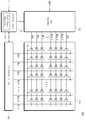
도 2는 본 발명에 따른 비휘발성 메모리 장치(100)의 제 1 실시 예를 보여주는 도면이다. 도 2를 참조하면, 비휘발성 메모리 장치(100)는 메모리 셀 어레이(110), 로우 디코더(120), 입출력 버퍼회로(130), 및 제어 로직(140)을 포함한다. 본 발명의 비휘발성 메모리 장치(100)는 프로그램 동작시 선택된 워드라인에 연결된 프로그램 셀들 및 프로그램 금지 셀들에 대하여 모든 데이터 검증을 수행하도록 제어 로직(140)을 포함한다. 여기서 프로그램 셀들은 데이터 변경을 위하여 문턱 전압이 변화되는 메모리 셀들이며, 프로그램 금지 셀들은 데이터 변경이 이루어지지 않도록 문턱 전압을 유지하는 메모리 셀들이다. 특히, 제어 로직(140)은 프 로그램 동작시 모든 데이터 검증에 대한 결과를 저장하는 페일 체크 레지스터(142)를 포함하고 있다.2 is a diagram illustrating a first embodiment of a
도 2에 도시된 비휘발성 메모리 장치(100)는 낸드 플래시 메모리이다. 그러나 본 발명의 비휘발성 메모리 장치는 낸드 플래시 메모리에 국한될 필요가 없다. 본 발명의 비휘발성 메모리 장치는 노아 플래시 메모리 장치, MRAM, PRAM, FRAM 등 다양한 종류의 비휘발성 메모리에 적용가능하다. 또한 본 발명의 비휘발성 메모리 장치는 3차원 어레이 구조(Three-Dimentional Array Structure)로 구현될 수 있다.The
메모리 셀 어레이(110)는 복수의 비트라인들(BL0~BLn-1) 및 복수의 워드라인들(WL0~WLm-1)과, 비트라인들 및 워드라인들이 교차하는 영역에 배치된 복수의 메모리 셀들을 포함한다. 여기서 메모리 셀들 각각에는 멀티 비트 데이터(multi bit dat)가 저장될 수 있다. 메모리 셀 어레이(110)는 복수의 메모리 블록들로 구성될 것이다. 도 2에는 단지 하나의 메모리 블록만이 도시되어 있다. 메모리 셀 어레이(110)의 각각의 메모리 블록들은 복수의 셀 스트링들을 포함하고 있다. 각 스트링은, 도 2에 도시된 바와 같이, 스트링 선택 트랜지스터, 그라운드 선택 트랜지스터, 및 스트링 선택 트랜지스터 및 그라운드 선택 트랜지스터 사이에 직렬 연결된 m개의 메모리 셀들로 구성된다.The
각 스트링의 스트링 선택 트랜지스터의 드레인은 대응하는 비트라인에 연결되고, 그라운드 선택 트랜지스터의 소스는 공통 소스 라인(CSL)에 연결된다. 스트링에 교차되도록 복수의 워드라인들(WL0~WLm-1)이 배열된다. 워드라인들(WL0~WLm-1)은 각 스트링의 대응하는 메모리 셀들에 각각 연결된다. 프로그램/읽기 전압을 선택된 워드라인에 인가함으로써 선택된 메모리 셀들로/로부터 데이터를 프로그램/읽기하는 것이 가능하다. 비트라인들(BL0~BLn-1)은 입출력 버퍼회로(130)의 페이지 버퍼들(도시되지 않음)에 전기적으로 연결된다.The drains of the string selection transistors of each string are connected to the corresponding bit lines, and the source of the ground selection transistors is connected to the common source line CSL. A plurality of word lines (WL0 to WLm-1) are arranged so as to intersect the strings. The word lines WL0 to WLm-1 are connected to corresponding memory cells of each string. It is possible to program / read data into / from selected memory cells by applying a program / read voltage to the selected word line. The bit lines BL0 to BLn-1 are electrically connected to page buffers (not shown) of the input /
로우 디코더(120)는 입력된 어드레스(ADDR)에 따라 메모리 블록을 선택하고, 선택된 메모리 블록의 구동될 워드라인을 선택한다. 예를 들어, 로우 디코더(120)는 프로그램 동작시 입력된 어드레스(ADDR)를 디코딩하여 선택된 메모리 블록에서 구동될 워드라인을 선택한다. 여기서 선택된 워드라인으로 고전압 발생기(도시되지 않음)로부터의 프로그램 전압이 인가된다.The
입출력 버퍼회로(130)는 프로그램 동작시 메모리 셀 어레이(110)에 로딩된 데이터를 임시로 저장하거나 읽기 동작시 메모리 셀 어레이(110)로부터 읽혀진 데이터를 임시로 저장하는 복수의 페이지 버퍼들(도시되지 않음)을 포함한다. 페이지 버퍼들 각각은 대응하는 비트라인들(BL0~BLn-1)을 통해 메모리 셀 어레이(110)와 연결된다.The input /
페이지 버퍼들은 프로그램 동작시 로딩된 데이터에 따라 비트라인으로 접지전압(예를 들어, 0V) 혹은 전원전압(Vcc)을 인가한다. 예를 들어, '0'의 데이터가 로딩된 페이지 버퍼와 연결된 비트라인(즉, 프로그램 셀과 연결된 비트라인)에는 접지전압(0V)이 인가된다. 그리고, '1'의 데이터가 로딩된 페이지 버퍼와 연결된 비트라인(즉,프로그램 금지 셀과 연결된 비트라인)에는 전원전압(Vcc)이 인가된다.The page buffers apply a ground voltage (e.g., 0 V) or a power supply voltage (Vcc) to the bit lines according to the data loaded during the program operation. For example, a ground voltage (0V) is applied to a bit line connected to a page buffer in which data of '0' is loaded (that is, a bit line connected to a program cell). The power supply voltage Vcc is applied to the bit line connected to the page buffer where the data of '1' is loaded (that is, the bit line connected to the program inhibit cell).
한편, 본 발명의 페이지 버퍼들은 프로그램 동작시 프로그램될 외부로부터 전송된 데이터 및 프로그램이 수행될 메모리 셀들에 이미 저장된 데이터를 읽어와 래치해 놓도록 구성된다.The page buffers of the present invention are configured to read and latch the data transmitted from the external to be programmed in the program operation and the data already stored in the memory cells in which the program is to be executed.
제어 로직(140)은 입력된 제어신호들(CTRL,예를 들어,/CE,/RE,/WE,CLE, ALE,/WP)에 응답하여 각 동작에 필요한 고전압들을 발생하여 로우 디코더(120)로 인가하고, 비휘발성 메모리 장치(100)의 내부 블록들의 모든 동작을 제어한다.The
제어 로직(140)은 프로그램 동작시 프로그램 셀들 및 프로그램 금지 셀들의 모든 데이터에 대하여 검증하도록 구현된다. 예를 들어, 제어 로직(140)은 프로그램 셀들의 데이터 '0'을 프로그램한 뒤 선택된 셀들의 데이터 '0'을 검증하고, 및 프로그램 금지 셀들의 데이터 '0'을 검증하도록 구성된다. 이때, 모든 데이터 검증 결과는 페일 체크 레지스터(142)에 저장된다. 페일 체크 레지스터(142)는 프로그램 셀들의 프로그램 성공 유무 및 프로그램 금지 셀들의 데이터 변경 유무를 저장한다. 만약, 프로그램 셀들 중 어느 하나가 프로그램에 성공하지 못하거나 프로그램 금지 셀들 중 어느 하나가 데이터 변경되면, 페일 체크 레지스터(142)는 프로그램 페일에 대응하는 비트들이 저장된다. 페일 체크 레지스터(142)는 프로그램 셀들에 대한 '0' 데이터 프로그램 성공 여부 및 프로그램 금지 셀들에 대한 '1' 데이터 검증 성공 여부를 저장하도록 구성된다.The
한편, 프로그램 페일이 발생할 경우, 다른 워드라인으로 프로그램 동작이 수행될 것이다. 아래에서는 이러한 프로그램 동작을 재프로그램 동작이라고 하겠다. 본 발명에서 재프로그램 동작은 외부의 메모리 제어기(도시되지 않음)에서 제어할 수 있도록 구현되거나 혹은 비휘발성 메모리 장치(100)의 제어 로직(140)에서 자체적으로 제어할 수 있도록 구현될 수 있다.On the other hand, if a program fail occurs, the program operation will be performed on another word line. In the following, we will call this program operation a reprogram operation. In the present invention, the reprogramming operation can be implemented to be controlled by an external memory controller (not shown) or can be controlled by the
첫째로, 메모리 제어기에서 재프로그램을 제어할 경우에는, 메모리 제어기는 페일 체크 레지스터(142)에 저장된 프로그램 페일 비트들을 읽고 그 결과에 따라 재프로그램 명령 및 새로운 어드레스를 휘발성 메모리 장치(100)로 전달한다. 이에 따라 비휘발성 메모리 장치(100)는 새로운 어드레스에 대응하는 워드라인으로 재프로그램 동작을 수행한다. 이때, 재프로그램될 데이터는 각각의 페이지 버퍼들에 이미 래치된 상태이기 때문에 별도로 외부로부터 전달받을 필요가 없다.First, when controlling the reprogramming in the memory controller, the memory controller reads the program fail bits stored in the
둘째로, 비휘발성 메모리 장치(100)에서 자체적으로 재프로그램을 제어할 경우에는, 제어 로직(140)은 페일 체크 레지스터(142)에 저장된 프로그램 페일 비트들을 읽고 그 결과에 따라 새로운 어드레스 대응하는 워드라인으로 재프로그램 동작을 수행한다. 이때, 재프로그램될 데이터는 각각의 페이지 버퍼들에게 이미 래치된 상태이기 때문에 별도로 외부로부터 전달받을 필요가 없다.Second, when controlling reprogramming itself in the
상술 된 바와 같이, 본 발명의 비휘발성 메모리 장치(100)은 재프로그램 발생시 별도로 외부로부터 프로그래될 데이터를 로딩할 필요가 없다.As described above, the
일반적인 비휘발성 메모리 장치에서는 프로그램 금지 셀들은 데이터 '1'의 페일 체크 동작을 수행하지 않는다. 따라서, 데이터 '1'의 페일 발생시 프로그램 페일이 발생하거나, 혹은 패스전압 윈도우의 특성 열화로 인하여 페일 비트 발생시 칩 레벨 혹은 시스템 레벨의 해결 방안이 없다.In general nonvolatile memory devices, the program inhibited cells do not fail-check operation of data '1'. Therefore, there is no solution of a chip level or a system level when fail bit is generated due to a program failure when a failure of data '1' occurs or a characteristic deterioration of a path voltage window.
반면에 본 발명의 비휘발성 메모리 장치(100)는 프로그램 셀들 및 프로그램 금지 셀들의 모든 데이터에 대한 검증을 수행하는 자가 진단(self diagonosis) 프로그램을 수행한다. 이러한 자가 진단 프로그램을 수행할 경우에는, 프로그램 페일 로 인하여 재 프로그램을 수행하더라도 외부로부터 다시 데이터를 로딩할 필요가 없다. 왜냐하면, 선택된 셀들 및 비선택된 셀들에 대응하는 데이터가 이미 페이지 버퍼에 로딩되어 있기 때문이다.On the other hand, the
이로써, 프로그램 실패로 인하여 재 프로그램을 고려한 프로그램 방법에 있어서, 본 발명의 프로그램 방법은 일반적인 프로그램 방법과 비교하여 프로그램 시간을 현저하게 줄일 수 있게 된다.Thus, in the program method considering reprogramming due to program failure, the program method of the present invention can significantly reduce the program time as compared with a general program method.
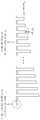
도 3은 본 발명의 비휘발성 메모리 장치(100)에 있어서 프로그램 방법을 보여주는 도면이다. 도 2 및 도 3을 참조하면, 프로그램 방법은 제 1 프로그램 시작 전압(Vpgm_start1)부터 시작하여 제 1 소정의 레벨큼(ΔVISPP1) 증가시키면서 선택된 워드라인으로 프로그램 전압을 인가한다. 즉, 비휘발성 메모리 장치(100)는 ISPP(Incremental Step Pluse Programming)으로 프로그램 동작을 수행한다.3 is a diagram showing a programming method in the
각 프로그램 루프에서 프로그램 전압 인가 후에는 프로그램 셀들에 대한 '0' 데이터 검증 동작이 수행된다. '0' 데이터 검증 동작이 모든 프로그램 셀들에 대하여 성공하면, 프로그램 금지 셀들에 대하여 '1' 데이터 검증 동작이 수행된다. 최종적으로 프로그램 동작이 성공되면, 프로그램 셀들은 데이터 '0'에 대응하는 문턱전압을 갖게 될 것이고, 프로그램 금지 셀들은 데이터 '1'에 대응하는 문턱전압을 유지하게 될 것이다.After a program voltage is applied in each program loop, a '0' data verify operation is performed on the program cells. If the '0' data verify operation is successful for all program cells, a '1' data verify operation is performed on the program inhibited cells. Finally, if the program operation is successful, the program cells will have a threshold voltage corresponding to data '0' and the program inhibit cells will maintain a threshold voltage corresponding to data '1'.
도 3에서는 프로그램 금지 셀들에 대한 '1' 데이터 검증 동작은 프로그램 셀들에 대한 '0' 데이터 프로그램 동작이 완료된 후 수행된다. 하지만, 본 발명의 비 휘발성 메모리 장치(100)의 '1' 데이터 검증은 반드시 프로그램 셀들에 대한 '0' 데이터 프로그램 동작 수행될 필요는 없다. 본 발명의 프로그램 금지 셀들에 대한 '1' 데이터 검증 동작은 각 프로그램 루프마다 혹은 미리 결정된 프로그램 루프 회수에만 수행될 수도 있다.In FIG. 3, the '1' data verification operation for the program inhibited cells is performed after the '0' data program operation for the program cells is completed. However, the '1' data verification of the
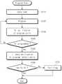
도 4는 도 2에 도시된 비휘발성 메모리 장치(100)의 프로그램 방법을 보여주는 제 1 흐름도이다. 도 2 내지 도 4를 참조하면, 프로그램 방법은 다음과 같이 진행된다.4 is a first flowchart showing a programming method of the
프로그램 동작시, 입력된 어드레스(ADDR)에 대응하는 워드라인이 선택된다. 또한 프로그램될 데이터가 페이지 버퍼들 각각에 로딩된다(S110). 로딩된 데이터에 따라 각각의 비트라인들(BL0~BLn-1)은 비트라인 셋업된다. 예를 들어, 프로그램 데이터 '0'이 로딩된 페이지 버퍼에 대응하는 비트라인들에는 프로그램 전압(0V)이 인가되고, 프로그램 금지 데이터 '1'이 로딩된 페이지 버퍼에 대응하는 비트라인들에는 프로그램 금지 전압(Vcc)이 인가된다.In the program operation, the word line corresponding to the input address ADDR is selected. The data to be programmed is also loaded into each of the page buffers (S110). Each of the bit lines BL0 to BLn-1 is set up in accordance with the loaded data. For example, the program voltage (0V) is applied to the bit lines corresponding to the page buffer loaded with the program data '0', and the bit lines corresponding to the page buffer loaded with the program inhibit data ' The voltage Vcc is applied.
이후, 선택된 워드라인에 연결된 메모리 셀들 중에서 프로그램 셀들에 대하여 데이터 '0' 프로그램 동작이 수행된다(S120). 도 3에 도시된 바와 같이, 프로그램 셀들이 연결된 선택된 워드라인으로 프로그램 시작 전압(Vpgm_start1)이 인가된다. 이후, 소정의 시간 후에 프로그램 셀들에 대한 '0' 데이터 검증 동작이 수행된다(S130). 여기서 '0' 데이터 검증 결과는 페일 체크 레지스터(142)에 저장된다. '0' 데이터 검증 동작 수행 결과로써, 프로그램 셀들 중 '0' 데이터 프로그램 동작이 완료된 메모리 셀들은 프로그램 금지된다. 예를 들어, '0' 데이터 프로그램 동 작이 완료된 메모리 셀들이 연결된 비트라인들로부터 전원전압(Vcc)이 인가될 것이다. 반면에, '0' 데이터 검증 동작 수행 결과로써, 프로그램 셀들 중 '0' 데이터 프로그램 동작이 완료되지 못한 메모리 셀들의 경우에는 소정의 레벨(ΔVISSP1)만큼 증가된 프로그램 전압을 선택된 워드라인으로 인가함으로 계속해서 프로그램 동작이 수행된다(S140).Thereafter, a data '0' program operation is performed on the program cells among the memory cells connected to the selected word line (S120). As shown in Fig. 3, the program start voltage Vpgm_start1 is applied to the selected word line to which the program cells are connected. Thereafter, a '0' data verification operation for the program cells is performed after a predetermined time (S130). Here, the '0' data verification result is stored in the
모든 프로그램 셀들이 '0' 데이터로 프로그램되면, 프로그램 금지 셀들에 대한 '1' 데이터 검증이 수행된다(S150). '0' 데이터 검증 결과에 따라 검증 동작이 성공했는지 판별된다(S160).If all the program cells are programmed with '0' data, '1' data verification for program inhibited cells is performed (S150). It is determined whether the verification operation is successful according to the '0' data verification result (S160).
만약 '1' 데이터 검증 동작이 실패하면, 프로그램 페일에 대응하는 플래그 비트가 페일 체크 레지스터(142)에 저장되고(S170), 프로그램 동작은 종료된다. 선택된 워드라인에 대한 프로그램 페일 발생시, 추후에 재프로그램이 수행될 것이다. 메모리 제어기(도시되지 않음)는 프로그램 종료 이후에 페일 체크 레지스터(142)에 저장된 플래그 비트를 읽기를 위한 읽기 명령을 비휘발성 메모리 장치(100)로 전달한다. 이때 전달된 읽기 명령에 의해 비휘발성 메모리 장치(100)는 페일 체크 레지스터(142)에 저장된 페일 정보를 메모리 제어기로 전송한다. 이에 메모리 제어기는 전송된 페일 체크 레지스터(142)의 플래그 비트를 통하여 프로그램 페일을 확인한다. 이때 전송된 플래그 비트가 프로그램 페일에 대응할 때에 메모리 제어기는 에러 정정이 가능한지를 판별한다. 만약 에러 정정이 가능하지 않다면, 메모리 제어기는 재프로그램 동작을 수행하도록 재프로그램 명령 및 새로운 어드레스를 비휘발성 메모리 장치(100)로 전달한다. 비휘발성 메모리 장치(100)는 새롭게 전송된 재 프로그램 명령 및 새로운 어드레스에 근거하여 프로그램 동작을 수행한다.If the '1' data verify operation fails, the flag bit corresponding to the program fail is stored in the fail check register 142 (S170) and the program operation is terminated. Upon occurrence of a program fail for the selected word line, a re-program will be performed at a later time. The memory controller (not shown) transfers a read command for reading the flag bit stored in the
만약 '1' 데이터 검증 동작이 성공하면, 선택된 워드라인에 대한 프로그램 동작이 완료된다.If the '1' data verify operation is successful, the program operation for the selected word line is completed.
본 발명에 따른 비휘발성 메모리 장치(100)의 프로그램 방법은 프로그램 셀들에 대하여 '0' 데이터 검증 동작 및 프로그램 금지 셀들에 대하여 '1' 데이터 검증 동작을 수행한다. 즉, 본 발명의 프로그램 방법은 메모리 셀들의 모든 데이터에 대한 검증 동작을 수행한다.The programming method of the
본 발명의 비휘발성 메모리 장치(100)는 외부로부터 제어되지 않고 자체적으로 재프로그램을 동작을 수행할 수도 있다. 도 5는 본 발명에 따른 비휘발성 메모리 장치(100)의 프로그램 방법을 보여주는 제 2 흐름도이다. 도 5에 도시된 프로그램 방법은 프로그램 페일 발생시 도 4에 도시된 바와 같이 프로그램 동작이 종료되지 않고, 곧 바로 다른 워드라인으로 프로그램 동작이 진행된다(S280). 본 발명의 비휘발성 메모리 장치(100)의 제어 로직(140)은 페일 체크 레지스터(142)에 저장된 플래그 비트에 따라 재프로그램 동작이 자체적으로 수행되도록 한다. 여기서 재프로그램 동작은 새로운 워드라인으로 도 5에 도시된 방법과 동일하게 진행될 것이다.The
도 6은 본 발명에 따른 비휘발성 메모리 장치(200)의 제 2 실시 예를 보여주는 도면이다. 본 발명의 비휘발성 메모리 장치(200)는 홀수번째 비트라인들(BLo1~BLon)에 연결된 메모리 셀들을 프로그램하고 짝수번째 비트라인들(BLe1~BLen)에 연결된 메모리 셀들을 프로그램한다. 특히, 비휘발성 메모리 장 치(100)는 선택된 비트라인들에 연결된 프로그램 금지 셀들에 대하여 '1' 데이터 검증 동작을 수행하고, 비선택된 비트라인들에 연결된 메모리 셀들에 대하여 '1' 및 '0' 데이터 검증 동작을 수행한다. 여기서 검증된 결과들은 페일 체크 레지스터(242)에 저장된다.Figure 6 is a diagram illustrating a second embodiment of a
도 7은 도 6에 도시된 비휘발성 메모리 장치(200)의 프로그램 방법을 보여주는 도면이다. 도 7을 참조하면, 프로그램 방법은 제 2 프로그램 시작 전압(Vpgm_start2)부터 시작하여 제 2 소정의 레벨만큼(ΔVISPP2) 증가시키면서 프로그램 전압을 선택된 워드라인으로 인가한다. 각 프로그램 루프마다 선택된 비트라인들에 연결된 프로그램 셀들 및 비선택된 비트라인들에 연결된 '0' 데이터 셀들에 대하여 '0' 데이터 검증 동작이 수행된다. 선택된 비트라인들에 연결된 모든 프로그램 셀들에 대하여 '0' 데이터 프로그램이 완료되면, 선택된 비트라인들에 연결된 프로그램 금지 셀들 및 비선택된 비트라인들에 연결된 '1' 데이터 셀들에 대하여 '1' 데이터 검증 동작이 수행된다. 최종적으로, 선택된 비트라인들에 연결된 프로그램 셀들에는 '0' 데이터가 프로그램되고, 선택된 비트라인들에 연결된 프로그램 금지 셀들에는 '1' 데이터가 유지되고, 비선택된 비트라인들에 연결된 메모리 셀들에는 각각 저장된 데이터가 유지된다.FIG. 7 is a diagram showing a programming method of the
본 발명의 프로그램 방법은 선택된 비트라인들에 연결된 프로그램 금지 셀들 및 비선택된 비트라인들에 연결된 메모리 셀들 각각에 저장된 데이터에 대응하는 검증 동작을 수행한다. 이로써, 프로그램 페일 진단이 강화된다.The programming method of the present invention performs a verify operation corresponding to data stored in each of the program inhibit cells coupled to the selected bit lines and each of the memory cells connected to the non-selected bit lines. This enhances the program fail diagnosis.
도 8은 도 6에 도시된 본 발명에 따른 비휘발성 메모리 장치(100)의 프로그 램 방법에 대한 제 1 흐름도이다. 도 6 내지 8을 참조하면, 프로그램 방법은 아래와 같다. 아래에서는 설명의 편의를 위하여 홀수번째 비트라인들(BLo1~BLon)에 연결된 메모리 셀들에는 이미 프로그램 동작이 수행되었고, 짝수번째 비트라인들(BLe1~BLen)에 연결된 메모리 셀들에 프로그램 동작이 수행된다고 가정하겠다. 즉, 아래에서 짝수번째 비트라인들(BLe1~BLen)이 선택된 비트라인들이고, 홀수번째 비트라인들(BLo1~BLon)이 비선택된 비트라인들이라고 가정하겠다.FIG. 8 is a first flowchart of a method of programming a
프로그램될 데이터가 외부로부터 로딩되어 각 짝수번째 페이지 버퍼들에 저장된다(S310). 여기서 짝수번째 페이지 버퍼들 각각은 짝수번째 비트라인들(BLe1~BLen)에 대응된다. 짝수번째 비트라인들(BLe1~BLen)에 연결된 메모리 셀들의 프로그램 동작이기 때문에 선택된 비트라인들은 짝수번째 비트라인(BLe1~BLen)이고, 비선택된 비트라인들은 홀수번째 비트라인들(BLo1~BLon)이다.Data to be programmed is loaded from the outside and stored in each even page buffer (S310). Here, each of the even-numbered page buffers corresponds to the even-numbered bit lines BLe1 to BLen. The selected bit lines are the even bit lines BLe1 to BLen and the unselected bit lines are the odd bit lines BLo1 to BLon because the program operation of the memory cells connected to the even bit lines BLe1 to BLen is performed .
데이터 로딩 후, 비선택된 홀수번째 비트라인(BLo1~BLon)에 연결된 메모리 셀들로부터 저장된 데이터를 읽는다(S320). 읽혀진 데이터는 각각 홀수번째 페이지 버퍼들에 래치된다. 이때 읽기 과정을 수행할 동안에는 비선택된 홀수번째 비트라인(BLoe1~BLon)이 활성화되도록 제어될 것이다.After the data loading, the stored data is read from the memory cells connected to the odd-numbered bit lines BLo1 to BLon (S320). The read data is latched in odd-numbered page buffers. At this time, during the reading process, the non-selected odd-numbered bit lines BLoe1 to BLon will be controlled to be activated.
이후, 짝수번째 페이지 버퍼들에 대응되는 짝수번째 비트라인들(BLe1~BLen)이 활성화됨으로, 프로그램 동작이 수행된다(S330). 소정 시간 동안 프로그램 동작이 수행된 후, 선택된 짝수번째 비트라인들(BLe1~BLen)에 연결된 프로그램 셀들 및 비선택된 홀수번째 비트라인들(BLo1~BLon)에 연결된 '0' 데이터 셀들에 대한 '0' 데이터 검증 동작이 수행된다(S340). '0' 데이터 검증 결과로써 '0' 데이터의 프로 그램이 완료되었는지 판별된다(S350). 만약, '0' 데이터 프로그램이 완료되지 못하면, 소정의 레벨만큼 프로그램 전압이 증가되고 상술 된 과정이 반복된다.Then, even-numbered bit lines BLe1 to BLen corresponding to the even-numbered page buffers are activated to perform the program operation (S330). 0 'data cells connected to the program cells connected to the selected even-numbered bit lines BLe1 to BLen and the non-selected odd-numbered bit lines BLo1 to BLon after the program operation is performed for a predetermined time, A data verify operation is performed (S340). As a result of the '0' data verification, it is determined whether the program of '0' data is completed (S350). If the '0' data program is not completed, the program voltage is increased by a predetermined level and the above-described process is repeated.
만약, '0' 데이터 프로그램이 완료되면, 선택된 짝수 비트라인들(BLe1~BLen)의 프로그램 금지 셀들 및 비선택된 홀수 비트라인들(BLo1~BLon)에 대한 '1' 데이터 검증 동작이 수행된다(S360).If the '0' data program is completed, a '1' data verify operation is performed on the program inhibited cells and unselected odd bit lines BLo1 to BLon of the selected even bit lines BLe1 to BLen (S360 ).
'1' 데이터 검증 결과로써 검증 동작이 판별된다(S370). '1' 데이터 검증이 실패하면 프로그램 동작은 페일이다. 따라서, 검증 동작 페일에 대응하는 플래그 비트가 페일 체크 레지스터(242)에 저장되고 프로그램 동작이 완료된다.As a result of the '1' data verification, the verification operation is determined (S370). If the '1' data verification fails, the program action is fail. Thus, the flag bit corresponding to the verify operation fail is stored in the
'1' 데이터 검증이 성공하면, 선택된 워드라인에 대한 짝수번째 비트라인들(BLe1~BLen)에 연결된 메모리 셀들에 대한 프로그램 동작이 완료된다.If the '1' data verification is successful, the program operation for the memory cells connected to the even bit lines BLe1 to BLen for the selected word line is completed.
도 9는 도 6에 도시된 비휘발성 메모리 장치(200)의 프로그램 방법에 대한 제 2 흐름도이다. 도 9의 S490 단계를 참조하면, 도 8과 비교하여 프로그램 페일 발생시 비휘발성 메모리 장치(200)는 자체적으로 재프로그램 동작을 수행한다. 제어 로직(240)은 페일 체크 레지스터(242)에 저장된 플래그 비트에 따라 재프로그램 여부를 결정한다.FIG. 9 is a second flowchart of the programming method of the
도 8 및 도 9에서는 각 프로그램 루프마다 비선택된 비트라인들에 연결된 '0' 데이터 셀들에 대하여 '0' 데이터 검증 동작이 수행된다. 하지만 본 발명의 프로그램 방법이 반드시 여기에 국한될 필요는 없다. 본 발명의 프로그램 방법은 각 프로그램 루프마다 선택된 비트라인들에 연결된 프로그램 셀들에 대하여만 '0' 데이터 검증 동작이 수행될 수도 있다. In FIGS. 8 and 9, a '0' data verify operation is performed on '0' data cells connected to bit lines not selected for each program loop. However, the programming method of the present invention is not necessarily limited thereto. The programming method of the present invention may perform a '0' data verification operation only for program cells connected to selected bit lines for each program loop.
도 10은 도 6에 도시된 비휘발성 메모리 장치(200)의 프로그램 방법에 대한 제 3 흐름도이다. 도 10을 참조하면, 각 프로그램 루프마다 선택된 비트라인들에 연결된 프로그램 셀들에 대하여만 '0' 데이터 검증 동작이 수행되고(S540), 선택된 비트라인들에 대한 '0' 데이터 프로그램이 완료되면 선택된 비트라인들 및 비선택된 비트라인들에 연결된 메모리 셀들에 대하여 모든 데이터 검증 동작이 수행된다(S560).10 is a third flowchart of the programming method of the
도 11은 도 9에 도시된 프로그램 방법에서 프로그램 페일시 다른 워드라인에 대한 프로그램 방법을 보여주는 흐름도이다. 도 6 및 11을 참조하면, 본 발명의 다른 워드라인에 대한 프로그램 방법은 다음과 같이 진행된다.FIG. 11 is a flowchart showing a programming method for another word line in a program failure in the programming method shown in FIG. 9. FIG. Referring to FIGS. 6 and 11, the programming method for another word line of the present invention proceeds as follows.
선택된 워드라인에 대한 프로그램 실패시, 제어 로직(240)은 새로운 워드라인에 대한 재프로그램 동작을 시작한다. 제어 로직(240)은 새로운 어드레스를 발생하여 로우 디코더(220)로 전달한다. 이때, 각 페이지 버퍼에는 선택된 비트라인들에 연결된 메모리 셀들에 대응하는 데이터 및 비선택된 비트라인들에 연결된 메모리 셀들에 대응하는 데이터가 래치되어 있다. 따라서 각 페이지 버퍼에 대응하는 비트라인이 프로그램 전압(0V) 혹은 프로그램 금지 전압(Vcc)으로 프리차지된다. 이후, 도 7에 도시된 바와 같이 새로운 어드레스로 인하여 선택된 새로운 워드라인으로 제 2 프로그램 시작 전압(Vpgm_start2)을 인가하여 '0' 데이터 프로그램이 수행된다(S491). 이후, 선택된 비트라인들 및 비선택된 비트라인들에 연결된 프로그램 셀들에 대하여 '0' 데이터 검증 동작이 수행된다(S192).Upon a program failure for the selected word line,
'0' 데이터 검증 동작으로 '0' 데이터 프로그램이 완료되었는 지 판별한 다(S193). 만약 '0' 데이터 검증 동작이 실패할 경우에는 선택된 새로운 워드라인으로 제 2 프로그램 시작 전압으로부터 제 2 소정의 레벨(ΔVISSP2)이 증가된 프로그램 전압을 인가하여 프로그램 동작이 계속된다.The '0' data verification operation determines whether the '0' data program is completed (S193). If the '0' data verify operation fails, the program operation is continued by applying a program voltage whose second predetermined level (? VISSP2) is increased from the second program start voltage to the selected new word line.
만약, 선택된 비트라인들 및 비선택된 비트라인들에 연결된 모든 프로그램 셀들이 '0' 데이터 프로그램될 때, 선택된 비트라인들 및 비선택된 비트라인들에 연결된 모든 프로그램 금지 셀들에 대하여 '1' 데이터 검증이 수행된다(S494).If all the program cells connected to the selected bit lines and the unselected bit lines are programmed with '0' data, '1' data verification is performed for all program inhibit cells connected to the selected bit lines and non-selected bit lines (S494).
제어 로직(240)은 '1' 데이터 검증 동작이 성공했는지 판별한다(S495). '1' 데이터 검증 동작이 성공하면, 다른 워드라인으로 프로그램 동작은 완료된다. 만약 '1' 데이터 검증 동작이 실패하면, 다른 워드라인으로 프로그램 동작이 실패한 것이다. 이에 따라 프로그램 페일에 대응하는 플래그 비트가 페일 체크 레지스터(242)에 저장된다(S496). 이후 제어 로직(240)는 또 다른 어드레스를 생성하고 이에 대응하는 워드라인으로 프로그램 동작을 수행한다.
도 12는 본 발명에 따른 페이지 버퍼의 기능을 보여주는 도면이다. 도 11를 참조하면, 본 발명의 페이지 버퍼들은 프로그램 동작시 비선택된 비트라인들에 연결된 메모리 셀들의 데이터를 읽어 저장하고, 또한 외부로부터 로딩된 데이터를 저장한다. 이렇게 페이지 버퍼에 저장된 데이터는 검증 동작시 데이터 체크를 하는데 이용된다.12 is a diagram illustrating the function of the page buffer according to the present invention. Referring to FIG. 11, the page buffers of the present invention read and store data of memory cells connected to non-selected bit lines during a program operation, and also store data loaded from the outside. The data stored in the page buffer is used to check the data during the verify operation.
본 발명은 프로그램 페일 발생시 다른 워드라인으로 재프로그램하는데 외부의 제어기로부터 데이터 입/출력을 필요치 않는다. 왜냐하면, 본 발명의 각 페이지 버퍼들은 선택된 셀들 및 비선택된 셀들의 데이터를 이미 저장하고 있기 때문이다.The present invention does not require data input / output from the external controller to reprogram the word line to another word line when a program fails. This is because each page buffer of the present invention already stores data of selected and non-selected cells.
도 13은 본 발명의 메모리 시스템(10)을 보여주는 도면이다. 도 13을 참조하면, 메모리 시스템(10)은 비휘발성 메모리 장치(12) 및 비휘발성 메모리 장치(12)을 제어하는 메모리 제어기(14)를 포함한다. 여기서 비휘발성 메모리 장치(12)은 도 2 및 도 6에 도시된 것과 동일한 기능을 수행한다.13 is a diagram showing a
일반적인 메모리 시스템에서는 데이터 '1' 및 비선택된 스트링의 데이터 '1' 혹은 '0'이 페일이 되었는지를 체크하지 않은 상태에서 비휘발성 메모리 장치의 프로그램 동작이 종료된다. 비휘발성 메모리 장치는 알앤비(R/B) 신호를 메모리 제어기로 전달하여 프로그램 종료를 알린다. 따라서 일반적인 메모리 시스템에서는 메모리 제어기가 프로그램 동작이 정상적으로 수행되었는지를 확인하기 위하여 해당 어드레스에 대응하는 데이터를 읽어 확인하고(예를 들어, ECC), 데이터 확인 결과로써 프로그램 페일이 체크되면 다른 어드레스에 대응하는 다른 워드라인으로 프로그램 동작을 수행한다. 이러한 과정에서 비휘발성 메모리 장치 및 메모리 제어기 사이에서는 적어도 2번 이상의 데이터 입출력 동작이 수행된다.In the general memory system, the program operation of the nonvolatile memory device is terminated without checking whether the data '1' and the data '1' or '0' of the non-selected string fail. The non-volatile memory device transmits an R / B signal to the memory controller to inform the program end. Accordingly, in a general memory system, the memory controller reads and confirms data corresponding to a corresponding address (for example, ECC) in order to check whether a program operation is normally performed, and if a program fail is checked as a result of data checking, And performs a program operation with another word line. In this process, at least two data input / output operations are performed between the nonvolatile memory device and the memory controller.
반면에 본 발명의 메모리 시스템(10)에서는 데이터 '1' 및 비선택된 스트링의 데이터 '1' 혹은 '0'의 페일이 되었는지를 비휘발성 메모리 장치(12)에서 점검하고 프로그램 동작이 종료된다. 프로그램 동작 결과로써, 프로그램 페일이 발생하면 비휘발성 메모리 장치(12)에서는 페이지 버퍼들 내부에 저장되어 있는 데이터를 이용하여 자체적으로 다른 워드라인으로 프로그램 동작이 수행된다. 따라서, 본 발명의 메모리 시스템(10)에서는 프로그램 페일이 발생하더라도 비휘발성 메모리 장치(12)와 메모리 제어기(14) 사이의 별도로 데이터 입출력 없이 다른 워드라인으로 프로그램 동작이 수행된다. 그 결과로써, 일반적인 메모리 시스템과 비교하여 본 발명의 메모리 시스템(10)은 프로그램 동작시 프로그램 페일로 발생되는 타임 오버헤드 문제를 크게 개선한다.On the other hand, in the
도 14는 일반적인 프로그램 방법과 본 발명의 프로그램 방법들의 재프로그램을 고려한 전체적인 프로그램 시간을 비교한 도면이다. 도 14를 참조하면, 본 발명의 프로그램 방법은 일반적인 프로그램 방법보다 시간 오버헤드를 크게 줄일 수 있게 된다. 도 14에 도시된 바와 같이, 일반적인 프로그램 방법은 7번의 데이터 입출력 시간이 사용되지만, 본 발명의 프로그램 방법은 한번의 데이터 입출력 시간이 사용된다.FIG. 14 is a diagram comparing the overall program time considering re-programming of the general programming method and the programming methods of the present invention. Referring to FIG. 14, the programming method of the present invention can significantly reduce time overhead compared to a general programming method. As shown in FIG. 14, seven data input / output times are used in a general programming method, but one data input / output time is used in the programming method of the present invention.
일반적인 프로그램 방법은 프로그램 실패가 발생 될 경우에 있어서 메모리 제어기와 비휘발성 메모리 장치 사이에 7번의 데이터 입출력 동작이 수행되어야 한다. 반면에 본 발명의 프로그램 방법은 프로그램 실패가 발생되더라도 메모리 제어기 및 비휘발성 메모리 장치 사이에 한번의 데이터 입출력 동작만 수행된다.In a typical programming method, seven data input / output operations must be performed between the memory controller and the nonvolatile memory device in the event of a program failure. On the other hand, even if a program failure occurs, only one data input / output operation is performed between the memory controller and the nonvolatile memory device.
본 발명의 제 1 프로그램 방법은 비휘발성 메모리 장치(12)에서 자체적으로 재프로그램 동작을 수행한다. 메모리 제어기(14)로부터 데이터를 입력받아 제 1 자가 진단 프로그램 동작을 수행하고, 이후부터 메모리 제어기(14)로/으로부터 별도의 데이터 입출력없이 제 2 자가 진단 프로그램 동작을 수행한다. 제 1 자가 진단 프로그램 동작에서는 선택된 셀들에 대하여 데이터 '0'이 프로그램 동작이 수행되고, 선택된 셀들에 대하여 '1' 데이터 검증 동작이 수행되고, 선택된 셀들 및 비선택된 셀들에 대하여 '0' 및 '1' 데이터 검증 동작이 수행된다. 여기서 선택된 메모 리 셀들은 선택된 비트라인들에 연결된 프로그램 셀들 및 프로그램 금지 셀들을 말하며, 비선택된 메모리 셀들은 비선택된 비트라인들에 연결된 메모리 셀들을 의미한다.The first programming method of the present invention performs the reprogramming operation itself in the
이후, 제 1 자가 진단 프로그램 동작 결과로써 프로그램 실패할 경우에는 제 2 자가 진단 프로그램 동작이 수행된다. 제 2 자가 진단 프로그램 동작에서는 메모리 제어기(14)로/로부터의 데이터 입출력 없이 선택된 셀들에 대하여 '0' 데이터 프로그램 동작이 수행되고, 비선택된 셀들에 대하여 이전 데이터가 프로그램된다. 상술 된 바와 같이 본 발명의 비휘발성 메모리 장치(12)는 프로그램 동작시 시간 오버헤드를 크게 줄일 수 있다.Thereafter, when the program fails as a result of the first self-diagnosis program operation, the second self-diagnosis program operation is performed. In the second self-diagnosis program operation, a '0' data program operation is performed for selected cells without data input / output to / from the
본 발명의 제 2 프로그램 방법은 메모리 제어기(14)에 의해 재프로그램 동작이 제어된다. 제 1 자가 진단 프로그램 동작 결과로써 프로그램 실패할 경우에 메모리 제어기(14)는 비휘발성 메모리 장치(12)의 페일 체크 레지스터에 저장된 플래그 비트 값에 따라 재프로그램 여부를 결정한다. 재프로그램이 결정되면, 재프로그램 명령(RP CMD) 및 새로운 어드레스를 비휘발성 메모리 장치(12)로 전달한다. 비휘발성 메모리 장치(12)는 새로운 어드레스에 대응하는 워드라인으로 제 2 자가 진단 프로그램 동작을 수행한다.In the second program method of the present invention, the reprogramming operation is controlled by the
본 발명에 따른 비휘발성 메모리 장치의 프로그램 방법은 프로그램 상태에 따른 추가적인 읽기/프로그램 동작을 제어기에서 수행하지 않고 비휘발성 메모리 장치 내에서 수행한다. 이로써, 프로그램 동작시 제어기 및 비휘발성 메모리 장치 사이의 데이터 입출력 회수를 줄일 수 있게 된다. 그 결과로써, 본 발명의 프로그 램 방법은 오버헤드 시간을 대폭 줄일 수 있게 된다. 이는 시스템 동작 특성의 향상된다.The method of programming a non-volatile memory device according to the present invention performs in the non-volatile memory device an additional read / program operation according to the program state, without performing it in the controller. This makes it possible to reduce the number of data input / output times between the controller and the nonvolatile memory device during the program operation. As a result, the program method of the present invention can significantly reduce the overhead time. This improves the system operating characteristics.
또한, 제어기의 소프트웨어 및 하드웨어 부담을 크게 줄일 수 있게 되고, 결과적으로 시스템의 비용이 감소된다.In addition, the software and hardware burden of the controller can be greatly reduced, and consequently the cost of the system is reduced.
본 발명의 프로그램 방법은 MLC 프로그램 방법에도 적용 가능하다. 일반적으로 MLC 프로그램 방법은 LSB 데이터가 저장되는 LSB 프로그램 동작과, MSB 데이터가 저장되는 MSB 프로그램 동작으로 구분된다. LSB 프로그램 동작은 도 1 내지 도 14에 상술 된 프로그램 방법으로 수행될 것이고, MSB 프로그램 동작은 도 1 내지 도 14에 상술 된 프로그램 방법을 응용하여 수행될 것이다. MSB 프로그램 동작 역시 프로그램 셀들에 대하여 변경될 데이터로 검증 동작을 수행하고, 프로그램 금지 셀들에 대하여 유지될 데이터로 검증 동작을 수행할 것이다. 특히 MSB 프로그램 동작시 LSB 데이터를 잃어버리지 않도록 각 페이지 버퍼들은 LSB 데이터를 읽어 저장해 둘 것이다. 이렇게 페이지 버퍼에 저장된 LSB 데이터는 LSB 데이터 복원 동작에 사용될 것이다.The program method of the present invention is also applicable to the MLC program method. Generally, the MLC program method is classified into an LSB program operation in which LSB data is stored and an MSB program operation in which MSB data is stored. The LSB program operation will be performed by the programming method described above with reference to Figs. 1 to 14, and the MSB program operation will be performed by applying the programming method described above with reference to Figs. The MSB program operation will also perform a verify operation with the data to be changed for the program cells and perform a verify operation with the data to be retained for the program inhibited cells. In particular, each page buffer will read and store the LSB data so that the LSB data is not lost during MSB program operation. Thus, the LSB data stored in the page buffer will be used for the LSB data restoration operation.
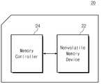
도 15는 본 발명에 따른 비휘발성 메모리 장치를 갖는 메모리 카드(20)를 보여주는 도면이다. 도 15를 참조하면, 메모리 카드(20)는 도 2 및 도 6에 도시된 구성과 실질적으로 동일하게 구성된 비휘발성 메모리 장치(22) 및 비휘발성 메모리 장치(22)를 제어하는 메모리 제어기(24)를 포함한다. 이러한 메모리 카드(20)는 디지털 카메라, PDA, 휴대용 오디오 장치, 휴대폰, 그리고 개인 컴퓨터와 같은 디지털 장치들과 더불어 정보를 저장하기/읽기 위해 사용된다.15 is a view showing a
도 16은 본 발명에 따른 비휘발성 메모리 장치를 갖는 메모리 시스템(30)을 보여주는 블록도이다. 도 16을 참조하면, 메모리 시스템(30)은 버스(31)에 전기적으로 연결된 중앙처리장치(32), 에스램(34), 메모리 제어기(36) 및 플래시 메모리 장치(38)를 포함한다. 여기서 플래시 메모리 장치(38)는 도 2 및 도 6에 도시된 것들과 실질적으로 동일하게 구성될 것이다. 플래시 메모리 장치(38)에는 중앙처리장치(32)에 의해서 처리된/처리될 N-비트 데이터(N은 1 또는 그보다 큰 정수)가 메모리 제어기(36)를 통해 저장될 것이다.16 is a block diagram illustrating a
비록 도면에는 도시되지 않았지만, 본 발명에 따른 메모리 시스템(20)에는 응용 칩셋(application chipset), 카메라 이미지 프로세서(Camera Image Processor: CIS), 모바일 디램, 등이 더 인가될 수 있음은 이 분야의 통상적인 지식을 습득한 자들에게 자명하다. 메모리 제어기와 플래시 메모리 장치는, 예를 들면, 데이터를 저장하는 데 비휘발성 메모리 장치를 사용하는 SSD(Solid State Drive/Disk)로 구성될 수도 있다.Although it is not shown in the drawings, application of an application chipset, a camera image processor (CIS), a mobile DRAM, and the like to the
본 발명에 따른 플래시 메모리 장치 그리고/또는 메모리 제어기는 다양한 형태들의 패키지를 이용하여 실장될 수 있다. 예를 들면, 본 발명에 따른 플래시 메모리 장치 그리고/또는 메모리 제어기는 PoP(Package on Package), Ball grid arrays(BGAs), Chip scale packages(CSPs), Plastic Leaded Chip Carrier(PLCC), Plastic Dual In-Line Package(PDIP), Die in Waffle Pack, Die in Wafer Form, Chip On Board(COB), Ceramic Dual In-Line Package(CERDIP), Plastic Metric Quad Flat Pack(MQFP), Thin Quad Flatpack(TQFP), Small Outline(SOIC), Shrink Small Outline Package(SSOP), Thin Small Outline(TSOP), Thin Quad Flatpack(TQFP), System In Package(SIP), Multi Chip Package(MCP), Wafer-level Fabricated Package(WFP), Wafer-Level Processed Stack Package(WSP), 등과 같은 패키지들을 이용하여 실장될 수 있다.The flash memory device and / or memory controller according to the present invention may be implemented using various types of packages. For example, the flash memory device and / or the memory controller according to the present invention can be implemented as a package on package, ball grid arrays (BGAs), chip scale packages (CSPs), plastic leaded chip carriers (PLCC) Linear Package (PDIP), Die in Waffle Pack, Die in Wafer Form, Chip On Board (COB), Ceramic Dual In-Line Package (CERDIP), Plastic Metric Quad Flat Pack (MQFP), Thin Quad Flatpack (SOIC), Shrink Small Outline Package (SSOP), Thin Small Outline (TSOP), Thin Quad Flatpack (TQFP), System In Package (SIP), Multi Chip Package (MCP), Wafer-level Fabricated Package Wafer-Level Processed Stack Package (WSP), and the like.
한편, 본 발명의 상세한 설명에서는 구체적인 실시예에 관하여 설명하였으나, 본 발명의 범위에서 벗어나지 않는 한도 내에서 여러 가지로 변형할 수 있다. 그러므로 본 발명의 범위는 상술한 실시예에 국한되어 정해져서는 안되며 후술하는 특허청구범위 뿐만 아니라 이 발명의 특허청구범위와 균등한 것들에 의해 정해져야 한다.While the invention has been shown and described with reference to certain preferred embodiments thereof, it will be understood by those skilled in the art that various changes and modifications may be made therein without departing from the spirit and scope of the invention. Therefore, the scope of the present invention should not be limited to the above-described embodiments, but should be determined by the equivalents of the claims of the present invention as well as the claims of the following.
도 1은 본 발명의 개념을 설명하기 위한 도면이다.1 is a diagram for explaining the concept of the present invention.
도 2는 본 발명에 따른 비휘발성 메모리 장치에 대한 제 1 실시 예를 보여주는 도면이다.2 is a view showing a first embodiment of a nonvolatile memory device according to the present invention.
도 3은 도 2에 도시된 비휘발성 메모리 장치의 ISPP 프로그램 방법을 보여주는 도면이다.FIG. 3 is a diagram illustrating an ISPP programming method of the nonvolatile memory device shown in FIG. 2. FIG.
도 4는 도 2에 도시된 비휘발성 메모리 장치의 프로그램 방법에 대한 제 1 흐름도이다.4 is a first flowchart of a programming method of the nonvolatile memory device shown in FIG.
도 5는 도 2에 도시된 비휘발성 메모리 장치의 프로그램 방법에 대한 제 2 흐름도이다.5 is a second flowchart of a programming method of the nonvolatile memory device shown in FIG.
도 6은 본 발명에 따른 비휘발성 메모리 장치에 대한 제 2 실시 예를 보여주는 도면이다.6 is a view showing a second embodiment of a nonvolatile memory device according to the present invention.
도 7은 도 6에 도시된 비휘발성 메모리 장치의 ISPP 프로그램 방법을 보여주는 도면이다.FIG. 7 is a diagram illustrating an ISPP programming method of the nonvolatile memory device shown in FIG. 6. FIG.
도 8은 도 6에 도시된 비휘발성 메모리 장치의 프로그램 방법에 대한 제 1 흐름도이다.8 is a first flowchart of a programming method of the nonvolatile memory device shown in FIG.
도 9는 도 6에 도시된 비휘발성 메모리 장치의 프로그램 방법에 대한 제 2 흐름도이다.9 is a second flowchart of a programming method of the nonvolatile memory device shown in FIG.
도 10은 도 6에 도시된 비휘발성 메모리 장치의 프로그램 방법에 대한 제 3 흐름도이다.10 is a third flowchart of a programming method of the nonvolatile memory device shown in FIG.
도 11은 도 9에 도시된 다른 워드라인으로의 프로그램 방법에 대한 흐름도이다.11 is a flowchart of a programming method to another word line shown in Fig.
도 12는 본 발명에 따른 페이지 버퍼의 기능을 보여주는 도면이다.12 is a diagram illustrating the function of the page buffer according to the present invention.
도 13는 본 발명에 따른 메모리 시스템을 보여주는 도면이다.13 is a diagram showing a memory system according to the present invention.
도 14는 일반적인 프로그램 방법과 본 발명의 프로그램 방법들의 재프로그램을 고려한 전체적인 프로그램 시간을 비교한 도면이다.FIG. 14 is a diagram comparing the overall program time considering re-programming of the general programming method and the programming methods of the present invention.
도 15는 본 발명의 비휘발성 메모리 장치를 갖는 메모리 카드를 보여주는 도면이다.15 is a view showing a memory card having the nonvolatile memory device of the present invention.
도 16은 본 발명의 비휘발성 메모리 장치를 갖는 컴퓨터 시스템에 관한 도면이다.16 is a diagram of a computer system having a nonvolatile memory device of the present invention.
*도면의 주요부분에 대한 부호의 설명*Description of the Related Art [0002]
100,200: 비휘발성 메모리 장치 110,110: 메모리 셀 어레이100, 200:
120,220: 로우 디코더 130,230: 입출력 버퍼회로120, 220:
140,240: 제어 로직 142,242: 페일 체크 레지스터140,240: Control logic 142,242: Failure check register
Claims (10)
Translated fromKoreanPriority Applications (2)
| Application Number | Priority Date | Filing Date | Title |
|---|---|---|---|
| KR1020080092856AKR101532754B1 (en) | 2008-09-22 | 2008-09-22 | Programming method of nonvolatile memory device |
| US12/543,993US8050101B2 (en) | 2008-09-22 | 2009-08-19 | Nonvolatile memory devices having erased-state verify capability and methods of operating same |
Applications Claiming Priority (1)
| Application Number | Priority Date | Filing Date | Title |
|---|---|---|---|
| KR1020080092856AKR101532754B1 (en) | 2008-09-22 | 2008-09-22 | Programming method of nonvolatile memory device |
Publications (2)
| Publication Number | Publication Date |
|---|---|
| KR20100033816A KR20100033816A (en) | 2010-03-31 |
| KR101532754B1true KR101532754B1 (en) | 2015-07-02 |
Family
ID=42037537
Family Applications (1)
| Application Number | Title | Priority Date | Filing Date |
|---|---|---|---|
| KR1020080092856AActiveKR101532754B1 (en) | 2008-09-22 | 2008-09-22 | Programming method of nonvolatile memory device |
Country Status (2)
| Country | Link |
|---|---|
| US (1) | US8050101B2 (en) |
| KR (1) | KR101532754B1 (en) |
Cited By (2)
| Publication number | Priority date | Publication date | Assignee | Title |
|---|---|---|---|---|
| US10699788B2 (en) | 2017-10-12 | 2020-06-30 | Samsung Electronics Co., Ltd. | Non-volatile memory device and operating method thereof for performing an erase detect operation |
| US11158381B2 (en) | 2017-10-12 | 2021-10-26 | Samsung Electronics Co., Ltd. | Non-volatile memory device and operating method thereof |
Families Citing this family (12)
| Publication number | Priority date | Publication date | Assignee | Title |
|---|---|---|---|---|
| KR100753156B1 (en) | 2006-09-13 | 2007-08-30 | 삼성전자주식회사 | Flash memory device and its memory cell array |
| KR101617641B1 (en)* | 2009-08-27 | 2016-05-03 | 삼성전자주식회사 | Nonvalatile memory device, memory system having its, and programming method thereof |
| US8385132B2 (en)* | 2010-12-22 | 2013-02-26 | Sandisk Technologies Inc. | Alternate bit line bias during programming to reduce channel to floating gate coupling in memory |
| KR101996004B1 (en) | 2012-05-29 | 2019-07-03 | 삼성전자주식회사 | Programming method of nonvolatile memory device and memory system having the same |
| DE102013105356A1 (en) | 2012-05-29 | 2013-12-05 | Samsung Electronics Co., Ltd. | Method for operating non-volatile memory device for use in smart-TV system, involves detecting errors generated during programming operation for programming portion of non-volatile multi-bit memory cells in non-volatile memory device |
| US20140198576A1 (en)* | 2013-01-16 | 2014-07-17 | Macronix International Co, Ltd. | Programming technique for reducing program disturb in stacked memory structures |
| JP6179206B2 (en)* | 2013-06-11 | 2017-08-16 | 株式会社リコー | Memory control device |
| KR20140144989A (en)* | 2013-06-12 | 2014-12-22 | 에스케이하이닉스 주식회사 | Memory system, semiconductor memory device and operating method thereof |
| KR102292217B1 (en)* | 2015-02-06 | 2021-08-24 | 삼성전자주식회사 | Memory device for performing internally data read verify, method thereof, and memory system having the same |
| US10381094B2 (en) | 2016-10-11 | 2019-08-13 | Macronix International Co., Ltd. | 3D memory with staged-level multibit programming |
| KR20190000562A (en)* | 2017-06-23 | 2019-01-03 | 에스케이하이닉스 주식회사 | Memory system and operation method thereof |
| US10354738B2 (en)* | 2017-09-27 | 2019-07-16 | Micron Technology, Inc. | One check fail byte (CFBYTE) scheme |
Citations (3)
| Publication number | Priority date | Publication date | Assignee | Title |
|---|---|---|---|---|
| KR100245413B1 (en)* | 1997-04-12 | 2000-03-02 | 윤종용 | Write method of non-volatile semiconductor memory device |
| KR20050072202A (en)* | 2004-01-06 | 2005-07-11 | 주식회사 테라반도체 | Non-volatile memory device and method for enhancing program speed thereof |
| KR100758300B1 (en)* | 2006-07-26 | 2007-09-12 | 삼성전자주식회사 | Flash memory device and its program method |
Family Cites Families (7)
| Publication number | Priority date | Publication date | Assignee | Title |
|---|---|---|---|---|
| KR0172408B1 (en)* | 1995-12-11 | 1999-03-30 | 김광호 | Non-volatile semiconductor memory and method driving the same |
| US7031192B1 (en)* | 2002-11-08 | 2006-04-18 | Halo Lsi, Inc. | Non-volatile semiconductor memory and driving method |
| US7073103B2 (en) | 2002-12-05 | 2006-07-04 | Sandisk Corporation | Smart verify for multi-state memories |
| JP2005353242A (en) | 2004-06-14 | 2005-12-22 | Toshiba Corp | Nonvolatile semiconductor memory device and data writing method thereof |
| US7403424B2 (en)* | 2005-03-31 | 2008-07-22 | Sandisk Corporation | Erasing non-volatile memory using individual verification and additional erasing of subsets of memory cells |
| US7436713B2 (en) | 2006-04-12 | 2008-10-14 | Sandisk Corporation | Reducing the impact of program disturb |
| DE602006011451D1 (en) | 2006-06-21 | 2010-02-11 | Hynix Semiconductor Inc | Method and device for the electrical programming of semiconductor memory cells |
- 2008
- 2008-09-22KRKR1020080092856Apatent/KR101532754B1/enactiveActive
- 2009
- 2009-08-19USUS12/543,993patent/US8050101B2/enactiveActive
Patent Citations (3)
| Publication number | Priority date | Publication date | Assignee | Title |
|---|---|---|---|---|
| KR100245413B1 (en)* | 1997-04-12 | 2000-03-02 | 윤종용 | Write method of non-volatile semiconductor memory device |
| KR20050072202A (en)* | 2004-01-06 | 2005-07-11 | 주식회사 테라반도체 | Non-volatile memory device and method for enhancing program speed thereof |
| KR100758300B1 (en)* | 2006-07-26 | 2007-09-12 | 삼성전자주식회사 | Flash memory device and its program method |
Cited By (3)
| Publication number | Priority date | Publication date | Assignee | Title |
|---|---|---|---|---|
| US10699788B2 (en) | 2017-10-12 | 2020-06-30 | Samsung Electronics Co., Ltd. | Non-volatile memory device and operating method thereof for performing an erase detect operation |
| US10957397B2 (en) | 2017-10-12 | 2021-03-23 | Samsung Electronics Co., Ltd. | Non-volatile memory device, storage device, and programming method thereof for performing an erase detect operation |
| US11158381B2 (en) | 2017-10-12 | 2021-10-26 | Samsung Electronics Co., Ltd. | Non-volatile memory device and operating method thereof |
Also Published As
| Publication number | Publication date |
|---|---|
| US8050101B2 (en) | 2011-11-01 |
| KR20100033816A (en) | 2010-03-31 |
| US20100074025A1 (en) | 2010-03-25 |
Similar Documents
| Publication | Publication Date | Title |
|---|---|---|
| KR101532754B1 (en) | Programming method of nonvolatile memory device | |
| KR100926475B1 (en) | Multi bit flash memory device and its program method | |
| JP4901348B2 (en) | Semiconductor memory device and control method thereof | |
| US8189393B2 (en) | Nonvolatile memory device with incremental step pulse programming | |
| JP5632210B2 (en) | Nonvolatile memory device and program method thereof | |
| KR101088235B1 (en) | Memory system having semiconductor memory and its data transfer method | |
| JP4510072B2 (en) | Nonvolatile semiconductor memory device and writing method thereof | |
| TWI602187B (en) | Semiconductor memory devices and memory systems | |
| KR101150645B1 (en) | Nonvolatile Semiconductor Memory Device | |
| JP4746658B2 (en) | Semiconductor memory system | |
| JP2012226806A (en) | Nonvolatile semiconductor storage device | |
| US8885419B2 (en) | Semiconductor memory device and methods of operating the same | |
| CN107766171A (en) | NAND flash memory and reading method thereof | |
| JP2011044200A (en) | Nonvolatile semiconductor memory | |
| US11024397B2 (en) | Nonvolatile memory device with verification signal to indicate success or failure of programming memory cell and method for operating thereof | |
| US8504896B2 (en) | Method of operating nonvolatile memory device and nonvolatile memory device for implementing the same | |
| CN114121118A (en) | Semiconductor memory device and method for operating semiconductor memory device | |
| US9213592B2 (en) | Semiconductor memory device and method of operating the same | |
| JP2012203943A (en) | Nonvolatile semiconductor memory device | |
| US8205039B2 (en) | Nonvolatile semiconductor memory device | |
| US12079075B2 (en) | Semiconductor storage apparatus and ECC related information reading method | |
| JPWO2007043133A1 (en) | Semiconductor device and control method thereof | |
| JP2006209963A (en) | Semiconductor memory device |
Legal Events
| Date | Code | Title | Description |
|---|---|---|---|
| PA0109 | Patent application | Patent event code:PA01091R01D Comment text:Patent Application Patent event date:20080922 | |
| PG1501 | Laying open of application | ||
| A201 | Request for examination | ||
| PA0201 | Request for examination | Patent event code:PA02012R01D Patent event date:20130916 Comment text:Request for Examination of Application Patent event code:PA02011R01I Patent event date:20080922 Comment text:Patent Application | |
| E902 | Notification of reason for refusal | ||
| PE0902 | Notice of grounds for rejection | Comment text:Notification of reason for refusal Patent event date:20150225 Patent event code:PE09021S01D | |
| E701 | Decision to grant or registration of patent right | ||
| PE0701 | Decision of registration | Patent event code:PE07011S01D Comment text:Decision to Grant Registration Patent event date:20150529 | |
| GRNT | Written decision to grant | ||
| PR0701 | Registration of establishment | Comment text:Registration of Establishment Patent event date:20150624 Patent event code:PR07011E01D | |
| PR1002 | Payment of registration fee | Payment date:20150625 End annual number:3 Start annual number:1 | |
| PG1601 | Publication of registration | ||
| FPAY | Annual fee payment | Payment date:20190530 Year of fee payment:5 | |
| PR1001 | Payment of annual fee | Payment date:20190530 Start annual number:5 End annual number:5 | |
| PR1001 | Payment of annual fee | Payment date:20230524 Start annual number:9 End annual number:9 | |
| PR1001 | Payment of annual fee | Payment date:20240527 Start annual number:10 End annual number:10 | |
| PR1001 | Payment of annual fee | Payment date:20250522 Start annual number:11 End annual number:11 |