KR101532376B1 - Apparatus for generating plasma using mutual inductive coupling, and apparatus for treating substrate comprising the same - Google Patents
Apparatus for generating plasma using mutual inductive coupling, and apparatus for treating substrate comprising the sameDownload PDFInfo
- Publication number
- KR101532376B1 KR101532376B1KR1020130143316AKR20130143316AKR101532376B1KR 101532376 B1KR101532376 B1KR 101532376B1KR 1020130143316 AKR1020130143316 AKR 1020130143316AKR 20130143316 AKR20130143316 AKR 20130143316AKR 101532376 B1KR101532376 B1KR 101532376B1
- Authority
- KR
- South Korea
- Prior art keywords
- electromagnetic field
- core
- plasma
- field applying
- reactance element
- Prior art date
- Legal status (The legal status is an assumption and is not a legal conclusion. Google has not performed a legal analysis and makes no representation as to the accuracy of the status listed.)
- Expired - Fee Related
Links
Images


Classifications
- H—ELECTRICITY
- H01—ELECTRIC ELEMENTS
- H01J—ELECTRIC DISCHARGE TUBES OR DISCHARGE LAMPS
- H01J37/00—Discharge tubes with provision for introducing objects or material to be exposed to the discharge, e.g. for the purpose of examination or processing thereof
- H01J37/32—Gas-filled discharge tubes
- H01J37/32009—Arrangements for generation of plasma specially adapted for examination or treatment of objects, e.g. plasma sources
- H01J37/32082—Radio frequency generated discharge
- H01J37/321—Radio frequency generated discharge the radio frequency energy being inductively coupled to the plasma
- H01J37/3211—Antennas, e.g. particular shapes of coils
- H—ELECTRICITY
- H01—ELECTRIC ELEMENTS
- H01J—ELECTRIC DISCHARGE TUBES OR DISCHARGE LAMPS
- H01J37/00—Discharge tubes with provision for introducing objects or material to be exposed to the discharge, e.g. for the purpose of examination or processing thereof
- H01J37/32—Gas-filled discharge tubes
- H01J37/32431—Constructional details of the reactor
- H01J37/3266—Magnetic control means
- H01J37/32669—Particular magnets or magnet arrangements for controlling the discharge
- H—ELECTRICITY
- H01—ELECTRIC ELEMENTS
- H01J—ELECTRIC DISCHARGE TUBES OR DISCHARGE LAMPS
- H01J37/00—Discharge tubes with provision for introducing objects or material to be exposed to the discharge, e.g. for the purpose of examination or processing thereof
- H01J37/32—Gas-filled discharge tubes
- H01J37/32009—Arrangements for generation of plasma specially adapted for examination or treatment of objects, e.g. plasma sources
- H01J37/32082—Radio frequency generated discharge
- H01J37/32174—Circuits specially adapted for controlling the RF discharge
Landscapes
- Physics & Mathematics (AREA)
- Engineering & Computer Science (AREA)
- Plasma & Fusion (AREA)
- Chemical & Material Sciences (AREA)
- Analytical Chemistry (AREA)
- Plasma Technology (AREA)
- Drying Of Semiconductors (AREA)
- Chemical Vapour Deposition (AREA)
Abstract
Translated fromKorean
Description
Translated fromKorean본 발명은 상호 유도 결합을 이용한 플라즈마 생성 장치 및 그를 포함하는 기판 처리 장치에 관한 것이다.BACKGROUND OF THE INVENTION 1. Field of the Invention The present invention relates to a plasma generating apparatus using mutual inductive coupling and a substrate processing apparatus including the plasma generating apparatus.
반도체, 디스플레이, 솔라셀 등을 제조하는 공정은 플라즈마를 이용하여 기판을 처리하는 공정을 포함한다. 예를 들어, 반도체 제조 공정 중에서 건식 식각에 사용되는 식각 장치 또는 애싱(ashing)에 사용되는 애싱 장치는 플라즈마를 생성하기 위한 챔버를 포함하며, 기판은 상기 플라즈마에 의해 식각 또는 애싱 처리될 수 있다.A process for manufacturing a semiconductor, a display, a solar cell, and the like includes a process of processing a substrate using a plasma. For example, an etching apparatus used for dry etching in a semiconductor manufacturing process or an ashing apparatus used for ashing may include a chamber for generating plasma, and the substrate may be etched or ashed by the plasma.
이러한 기판 처리 장치는 챔버에 설치된 코일에 시변 전류를 흘려 챔버 내에 전자기장을 유도하고, 유도된 전자기장을 이용하여 챔버에 공급된 가스로부터 플라즈마를 발생시킨다.Such a substrate processing apparatus induces an electromagnetic field in the chamber by passing a time-varying current through a coil provided in the chamber, and generates a plasma from the gas supplied to the chamber using the induced electromagnetic field.
최근 직경이 450 mm에 달하는 대면적 기판을 처리하는 공정이 도입되면서 공정의 수율 저하가 큰 이슈로 대두되고 있다. 특히, 플라즈마 공정의 수율을 높이기 위해서는 챔버 전체에 걸쳐 플라즈마를 균일하게 생성하는 것이 요구된다. 하지만, 단일 유도 코일 구조의 플라즈마 장비는 코일의 입력단 전압이 접지단 전압보다 높아 코일 전체에 걸쳐 전압이 불균형하게 분포하며, 이로 인해 챔버 내에 플라즈마가 불균일하게 생성되는 문제가 발생한다.In recent years, a process for processing a large-area substrate having a diameter of 450 mm has been introduced, leading to a problem of lowering the yield of the process. Particularly, in order to increase the yield of the plasma process, it is required to uniformly generate the plasma over the entire chamber. However, in the plasma equipment of the single induction coil structure, since the input terminal voltage of the coil is higher than the ground terminal voltage, the voltage is unevenly distributed over the entire coil, thereby causing a problem of non-uniform plasma generation in the chamber.
본 발명의 실시예는 챔버 내에 플라즈마를 균일하게 발생시키는 플라즈마 생어 장치 및 그를 포함하는 기판 처리 장치를 제공하는 것을 목적으로 한다.It is an object of the present invention to provide a plasma biofouling apparatus for uniformly generating plasma in a chamber and a substrate processing apparatus including the same.
본 발명의 실시예는 대면적의 기판을 처리하는 경우 공정의 수율을 향상시킬 수 있는 플라즈마 생성 장치 및 그를 포함하는 기판 처리 장치를 제공하는 것을 목적으로 한다.It is an object of the present invention to provide a plasma generating apparatus and a substrate processing apparatus including the same that can improve the yield of a process when a substrate having a large area is processed.
본 발명의 일 실시예에 따른 플라즈마 생성 장치는, RF 신호를 공급하는 RF 전원; 상기 RF 신호를 공급받아 전자장을 유도하는 다수의 전자장 인가기; 및 상기 전자장 인가기의 접지단에 연결되는 리액턴스 소자를 포함하며, 각각의 전자장 인가기는 상호 유도 결합된 다수의 코일을 포함할 수 있다.According to an embodiment of the present invention, there is provided a plasma generating apparatus including: an RF power supply for supplying an RF signal; A plurality of electromagnetic field applying units for receiving the RF signal to induce an electromagnetic field; And a reactance element coupled to a ground terminal of the electromagnetic field applicator, wherein each electromagnetic field applicator may comprise a plurality of coils coupled together.
상기 다수의 전자장 인가기는 서로 직렬로 연결될 수 있다.The plurality of electromagnetic field applying units may be connected to each other in series.
각각의 전자장 인가기에 포함된 코일들은 권선 수가 동일할 수 있다.The coils included in each electromagnetic field applicator may have the same number of windings.
상기 전자장 인가기는: 자성체로 구성된 코어; 상기 코어의 일부분에 감긴 제 1 코일; 및 상기 코어의 타부분에 감긴 제 2 코일;을 포함할 수 있다.The electromagnetic field applying device includes: a core composed of a magnetic material; A first coil wound around a portion of the core; And a second coil wound around the other portion of the core.
상기 코어는: 제 1 폐루프를 형성하는 제 1 코어; 및 제 2 폐루프를 형성하는 제 2 코어;를 포함할 수 있다.The core comprising: a first core forming a first closed loop; And a second core forming a second closed loop.
상기 제 1 코어는: 상기 제 1 폐루프의 절반부를 형성하는 제 1 서브 코어; 및 상기 제 1 폐루프의 나머지 절반부를 형성하는 제 2 서브 코어를 포함하고, 상기 제 2 코어는: 상기 제 2 폐루프의 절반부를 형성하는 제 3 서브 코어; 및 상기 제 2 폐루프의 나머지 절반부를 형성하는 제 4 서브 코어를 포함할 수 있다.The first core comprising: a first sub-core forming a half of the first closed loop; And a second sub-core forming the other half of said first closed loop, said second core comprising: a third sub-core forming a half of said second closed loop; And a fourth sub-core forming the other half of the second closed loop.
상기 제 1 서브 코어와 상기 제 2 서브 코어 사이, 그리고 상기 제 3 서브 코어와 상기 제 4 서브 코어 사이에는 절연체가 삽입될 수 있다.An insulator may be inserted between the first sub-core and the second sub-core, and between the third sub-core and the fourth sub-core.
상기 RF 전원과 상기 다수의 전자장 인가기 간의 노드들에 구비되어 각 노드에서 상기 RF 신호의 위상을 동일하게 고정시키는 위상 조절기를 더 포함할 수 있다.And a phase adjuster provided at nodes between the RF power source and the plurality of electromagnetic field applying units to fix the phase of the RF signal at each node equally.
상기 다수의 전자장 인가기 간의 노드들에 연결된 분로(shunt) 리액턴스 소자를 더 포함할 수 있다.And a shunt reactance element coupled to nodes between the plurality of electromagnetic field application devices.
상기 분로 리액턴스 소자의 임피던스는 상기 상호 유도 결합된 코일들 중 2차 코일과 상기 리액턴스 소자의 합성 임피던스의 절반일 수 있다.The impedance of the shunt reactance element may be half of the combined impedance of the secondary coil and the reactance element among the mutually inductively coupled coils.
상기 리액턴스 소자는 가변 커패시터를 포함할 수 있다.The reactance element may comprise a variable capacitor.
본 발명의 일 실시예에 따른 기판 처리 장치는, 내부에 기판이 배치되는 공정 챔버를 포함하며, 공정이 수행되는 공간을 제공하는 공정 유닛; 플라즈마를 발생시켜 상기 공정 유닛으로 플라즈마를 제공하는 플라즈마 발생 유닛; 및 상기 공정 유닛 내부의 가스 및 반응 부산물을 배출하는 배기 유닛을 포함하며, 상기 플라즈마 발생 유닛은: RF 신호를 공급하는 RF 전원; 상기 RF 신호를 공급받아 전자장을 유도하는 다수의 전자장 인가기; 상기 전자장 인가기가 배치되며, 플라즈마가 생성되는 공간을 제공하는 플라즈마 챔버; 및 상기 전자장 인가기의 접지단에 연결되는 리액턴스 소자를 포함하며, 각각의 전자장 인가기는 상호 유도 결합된 다수의 코일을 포함할 수 있다.A substrate processing apparatus according to an embodiment of the present invention includes: a processing unit including a processing chamber in which a substrate is disposed, the processing unit providing a space in which processing is performed; A plasma generating unit for generating a plasma to supply a plasma to the processing unit; And an exhaust unit for exhausting gas and reaction by-products in the processing unit, wherein the plasma generating unit comprises: an RF power supply for supplying an RF signal; A plurality of electromagnetic field applying units for receiving the RF signal to induce an electromagnetic field; A plasma chamber in which the electromagnetic field applicator is disposed and which provides a space in which plasma is generated; And a reactance element coupled to a ground terminal of the electromagnetic field applicator, wherein each electromagnetic field applicator may comprise a plurality of coils coupled together.
상기 다수의 전자장 인가기는 서로 직렬로 연결될 수 있다.The plurality of electromagnetic field applying units may be connected to each other in series.
각각의 전자장 인가기에 포함된 코일들은 권선 수가 동일할 수 있다.The coils included in each electromagnetic field applicator may have the same number of windings.
상기 플라즈마 챔버는 둘레에 다수의 절연 루프를 가지며, 상기 전자장 인가기는: 자성체로 구성되며, 상기 절연 루프의 제 1 부분을 감싸는 제 1 코어; 상기 자성체로 구성되며, 상기 절연 루프의 제 2 부분을 감싸는 제 2 코어; 상기 제 1 코어와 상기 제 2 코어의 일부분에 감긴 1차 코일; 및 상기 제 1 코어와 상기 제 2 코어의 타부분에 감긴 2차 코일;을 포함할 수 있다.Wherein the plasma chamber has a plurality of insulating loops around it, the electromagnetic field applicator comprising: a first core comprising a magnetic body and surrounding a first portion of the insulating loop; A second core composed of the magnetic body, the second core surrounding the second portion of the insulating loop; A primary coil wound around the first core and a portion of the second core; And a secondary coil wound around the first core and the other portion of the second core.
상기 제 1 코어는: 상기 절연 루프의 제 1 부분 중 상반부를 감싸는 제 1 상측 코어; 상기 절연 루프의 제 1 부분 중 하반부를 감싸는 제 1 하측 코어를 포함하고, 상기 제 2 코어는: 상기 절연 루프의 제 2 부분 중 상반부를 감싸는 제 2 상측 코어; 및 상기 절연 루프의 제 2 부분 중 하반부를 감싸는 제 2 하측 코어를 포함할 수 있다.The first core comprising: a first upper core surrounding the upper half of the first portion of the insulating loop; And a first lower core surrounding the lower half of the first portion of the insulating loop, the second core comprising: a second upper core surrounding the upper half of the second portion of the insulating loop; And a second lower core surrounding the lower half of the second portion of the insulating loop.
상기 제 1 상측 코어와 상기 제 1 하측 코어 사이, 그리고 상기 제 2 상측 코어와 상기 제 2 하측 코어 사이에는 절연체가 삽입될 수 있다.An insulator may be inserted between the first upper core and the first lower core, and between the second upper core and the second lower core.
상기 플라즈마 발생 유닛은: 상기 RF 전원과 상기 다수의 전자장 인가기 간의 노드들에 구비되어 각 노드에서 상기 RF 신호의 위상을 동일하게 고정시키는 위상 조절기를 더 포함할 수 있다.The plasma generating unit may further include a phase adjuster provided at nodes between the RF power source and the plurality of electromagnetic field applying units to fix the phase of the RF signal at each node equally.
상기 플라즈마 발생 유닛은: 상기 다수의 전자장 인가기 간의 노드들에 연결된 분로 리액턴스 소자를 더 포함할 수 있다.The plasma generating unit may further comprise: a shunting reactance element connected to nodes between the plurality of electromagnetic field applying units.
상기 분로 리액턴스 소자의 임피던스는 상기 상호 유도 결합된 코일들 중 2차 코일과 상기 리액턴스 소자의 합성 임피던스의 절반일 수 있다.The impedance of the shunt reactance element may be half of the combined impedance of the secondary coil and the reactance element among the mutually inductively coupled coils.
상기 리액턴스 소자는 가변 커패시터를 포함할 수 있다.The reactance element may comprise a variable capacitor.
본 발명의 실시예에 따르면, 챔버 내에 플라즈마를 균일하게 생성할 수 있다. 특히, 대면적의 기판을 처리하기 위한 대형 챔버에서도 플라즈마를 균일하게 생성할 수 있다.According to the embodiment of the present invention, plasma can be uniformly generated in the chamber. Particularly, even in a large chamber for processing a substrate having a large area, plasma can be uniformly generated.
본 발명의 실시예에 따르면, 대면적의 기판을 처리하는 경우 공정의 수율을 향상시킬 수 있다.According to the embodiment of the present invention, the yield of the process can be improved when a large-area substrate is processed.
도 1은 본 발명의 일 실시예에 따른 기판 처리 장치를 예시적으로 나타내는 개략도다.
도 2는 본 발명의 일 실시예에 따른 플라즈마 발생 유닛의 평면 모습을 나타내는 예시적인 도면이다.
도 3은 본 발명의 일 실시예에 따른 전자장 인가기의 정면 모습을 나타내는 예시적인 도면이다.
도 4는 본 발명의 일 실시예에 따른 플라즈마 발생 유닛의 등가 회로도다.
도 5는 본 발명의 다른 실시예에 따른 플라즈마 발생 유닛의 등가 회로도다.
도 6은 본 발명의 또 다른 실시예에 따른 플라즈마 발생 유닛의 등가 회로도다.
도 7은 본 발명의 또 다른 실시예에 따른 플라즈마 발생 유닛의 평면 모습을 나타내는 예시적인 도면이다.
도 8은 본 발명의 또 다른 실시예에 따른 전자장 인가기의 정면 모습을 나타내는 예시적인 도면이다.
도 9는 본 발명의 또 다른 실시예에 따른 플라즈마 발생 유닛의 등가 회로도다.FIG. 1 is a schematic view exemplarily showing a substrate processing apparatus according to an embodiment of the present invention. FIG.
2 is an exemplary diagram showing a plan view of a plasma generating unit according to an embodiment of the present invention.
3 is an exemplary diagram showing a front view of an electric field applicator according to an embodiment of the present invention.
4 is an equivalent circuit diagram of a plasma generating unit according to an embodiment of the present invention.
5 is an equivalent circuit diagram of a plasma generating unit according to another embodiment of the present invention.
6 is an equivalent circuit diagram of a plasma generating unit according to another embodiment of the present invention.
7 is an exemplary view showing a plan view of a plasma generating unit according to another embodiment of the present invention.
8 is an exemplary diagram showing a front view of an electric field applicator according to another embodiment of the present invention.
9 is an equivalent circuit diagram of a plasma generating unit according to another embodiment of the present invention.
본 발명의 다른 이점 및 특징, 그리고 그것들을 달성하는 방법은 첨부되는 도면과 함께 상세하게 후술 되는 실시 예를 참조하면 명확해질 것이다. 그러나 본 발명은 이하에서 개시되는 실시 예에 한정되는 것이 아니라 서로 다른 다양한 형태로 구현될 수 있으며, 단지 본 실시 예는 본 발명의 개시가 완전하도록 하고, 본 발명이 속하는 기술분야에서 통상의 지식을 가진 자에게 발명의 범주를 완전하게 알려주기 위해 제공되는 것이며, 본 발명은 청구항의 범주에 의해 정의될 뿐이다.Other advantages and features of the present invention and methods of achieving them will become apparent with reference to the embodiments described below in detail with reference to the accompanying drawings. The present invention may, however, be embodied in many different forms and should not be construed as being limited to the embodiments set forth herein. Rather, these embodiments are provided so that this disclosure will be thorough and complete, and will fully convey the concept of the invention to those skilled in the art. Is provided to fully convey the scope of the invention to those skilled in the art, and the invention is only defined by the scope of the claims.
만일 정의되지 않더라도, 여기서 사용되는 모든 용어들(기술 혹은 과학 용어들을 포함)은 이 발명이 속한 종래 기술에서 보편적 기술에 의해 일반적으로 수용되는 것과 동일한 의미를 가진다. 일반적인 사전들에 의해 정의된 용어들은 관련된 기술 그리고/혹은 본 출원의 본문에 의미하는 것과 동일한 의미를 갖는 것으로 해석될 수 있고, 그리고 여기서 명확하게 정의된 표현이 아니더라도 개념화되거나 혹은 과도하게 형식적으로 해석되지 않을 것이다.Unless defined otherwise, all terms (including technical or scientific terms) used herein have the same meaning as commonly accepted by the generic art in the prior art to which this invention belongs. Terms defined by generic dictionaries may be interpreted to have the same meaning as in the related art and / or in the text of this application, and may be conceptualized or overly formalized, even if not expressly defined herein I will not.
본 명세서에서 사용된 용어는 실시 예들을 설명하기 위한 것이며 본 발명을 제한하고자 하는 것은 아니다. 본 명세서에서, 단수형은 문구에서 특별히 언급하지 않는 한 복수형도 포함한다. 명세서에서 사용되는 '포함한다' 및/또는 이 동사의 다양한 활용형들 예를 들어, '포함', '포함하는', '포함하고', '포함하며' 등은 언급된 조성, 성분, 구성요소, 단계, 동작 및/또는 소자는 하나 이상의 다른 조성, 성분, 구성요소, 단계, 동작 및/또는 소자의 존재 또는 추가를 배제하지 않는다. 본 명세서에서 '및/또는' 이라는 용어는 나열된 구성들 각각 또는 이들의 다양한 조합을 가리킨다.The terminology used herein is for the purpose of illustrating embodiments and is not intended to be limiting of the present invention. In the present specification, the singular form includes plural forms unless otherwise specified in the specification. As used herein, the terms' comprise 'and / or various forms of use of the verb include, for example,' including, '' including, '' including, '' including, Steps, operations, and / or elements do not preclude the presence or addition of one or more other compositions, components, components, steps, operations, and / or components. The term 'and / or' as used herein refers to each of the listed configurations or various combinations thereof.
이하, 본 명세서에 첨부된 도면을 참조하여 본 발명의 실시예를 상세하게 설명하기로 한다.Hereinafter, embodiments of the present invention will be described in detail with reference to the drawings attached hereto.
도 1은 본 발명의 일 실시예에 따른 기판 처리 장치(10)를 예시적으로 나타내는 개략도다.Fig. 1 is a schematic view exemplarily showing a
도 1을 참조하면, 상기 기판 처리 장치(10)는 플라즈마를 이용하여 기판(W) 상의 박막을 처리, 예컨대 식각 또는 애싱(ashing)할 수 있다. 식각 또는 애싱하고자 하는 박막은 질화막일 수 있다. 일 예에 따르면, 질화막은 실리콘 질화막(Silicon nitride)일 수 있다.Referring to FIG. 1, the
상기 기판 처리 장치(10)는 공정 유닛(100), 배기 유닛(200) 및 플라즈마 발생 유닛(300)을 가질 수 있다. 공정 유닛(100)은 기판이 놓이고 식각 또는 애싱 공정이 수행되는 공간을 제공할 수 있다. 배기 유닛(200)은 공정 유닛(100) 내부에 머무르는 공정 가스 및 기판 처리 과정에서 발생한 반응 부산물 등을 외부로 배출하고, 공정 유닛(100) 내의 압력을 설정 압력으로 유지할 수 있다. 플라즈마 발생 유닛(300)은 외부에서 공급되는 공정 가스로부터 플라즈마를 생성하고, 이를 공정 유닛(100)으로 공급할 수 있다.The
공정 유닛(100)은 공정 챔버(110), 기판 지지부(120), 그리고 배플(130)을 가질 수 있다. 공정 챔버(110)의 내부에는 기판 처리 공정을 수행하는 처리 공간(111)이 형성될 수 있다. 공정 챔버(110)는 상부벽이 개방되고, 측벽에는 개구(미도시)가 형성될 수 있다. 기판은 개구를 통하여 공정 챔버(110)에 출입할 수 있다. 개구는 도어(미도시)와 같은 개폐 부재에 의해 개폐될 수 있다. 공정 챔버(110)의 바닥면에는 배기홀(112)이 형성될 수 있다. 배기홀(112)은 배기유닛(200)과 연결되며, 공정 챔버(110) 내부에 머무르는 가스와 반응 부산물이 외부로 배출되는 통로를 제공할 수 있다.
기판 지지부(120)는 기판(W)을 지지할 수 있다. 기판 지지부(120)는 서셉터(121)와 지지축(122)을 포함할 수 있다. 서셉터(121)는 처리 공간(111) 내에 위치되며 원판 형상으로 제공될 수 있다. 서셉터(121)는 지지축(122)에 의해 지지될 수 있다. 기판(W)은 서셉터(121)의 상면에 놓일 수 있다. 서셉터(121)의 내부에는 전극(미도시)이 제공될 수 있다. 전극은 외부 전원과 연결되며, 인가된 전력에 의해 정전기를 발생시킬 수 있다. 발생된 정전기는 기판(W)을 서셉터(121)에 고정시킬 수 있다. 서셉터(121)의 내부에는 가열부재(125)가 제공될 수 있다. 일 예에 의하면, 가열부재(125)는 히팅 코일일 수 있다. 또한, 서셉터(121)의 내부에는 냉각부재(126)가 제공될 수 있다. 냉각부재는 냉각수가 흐르는 냉각라인으로 제공될 수 있다. 가열부재(125)는 기판(W)을 기 설정된 온도로 가열할 수 있다. 냉각부재(126)는 기판(W)을 강제 냉각시킬 수 있다. 공정 처리가 완료된 기판(W)은 상온 상태 또는 다음 공정 진행에 요구되는 온도로 냉각될 수 있다.The
배플(130)은 서셉터(121)의 상부에 위치할 수 있다. 배플(130)에는 홀(131)들이 형성될 수 있다. 홀(131)들은 배플(130)의 상면에서 하면까지 제공되는 관통홀로 제공되며, 배플(130)의 각 영역에 균일하게 형성될 수 있다.The
다시 도 1을 참조하면, 플라즈마 발생 유닛(300)은 공정 챔버(110)의 상부에 위치할 수 있다. 플라즈마 발생 유닛(300)은 소스 가스를 방전시켜 플라즈마를 생성하고, 생성된 플라즈마를 처리 공간(111)으로 공급할 수 있다. 플라즈마 발생 유닛(300)은 RF 전원(310), 플라즈마 챔버(320), 절연 루프(330) 및 전자장 인가기(340)를 포함할 수 있다. 나아가, 상기 플라즈마 발생 유닛(300)은 소스 가스 공급부(360)를 더 포함할 수 있다.Referring again to FIG. 1, the
플라즈마 챔버(320)는 공정 챔버(110)의 상부에 위치되어 공정 챔버(110)에 결합될 수 있다. 플라즈마 챔버(320)의 상단은 소스 가스 공급부(360)와 연결될 수 있다. 소스 가스는 플라즈마 챔버(320) 내 방전 공간으로 공급될 수 있다. 소스 가스는 이불화메탄(CH2F2, Difluoromethane), 질소(N2), 그리고 산소(O2)를 포함할 수 있다. 선택적으로 소스 가스는 사불화탄소(CF4, Tetrafluoromethane) 등 다른 종류의 가스를 더 포함할 수도 있다.The
전자장 인가기(340)는 절연 루프(330)를 통해 플라즈마 챔버(320)의 측벽에 설치될 수 있다. RF 전원(310)은 전자장 인가기(340)에 고주파 전류를 공급할 수 있다. 고주파 전류에 의해 방전 공간에는 유도 전기장이 형성되고, 방전 공간 내 소스 가스는 유도 전기장으로부터 이온화에 필요한 에너지를 얻어 플라즈마 상태로 변환될 수 있다. 전자장 인가기(340)의 접지단에는 리액턴스 소자, 예컨대 커패시터(350)가 연결될 수 있으나, 실시예에 따라 커패시터가 연결되지 않고 곧바로 접지에 연결될 수도 있다.The electromagnetic
플라즈마 발생 유닛(300)의 구조는 상술한 예에 한정되지 않고, 소스 가스로부터 플라즈마를 발생시키기 위한 다양한 구조가 사용될 수 있다.The structure of the
도 2는 본 발명의 일 실시예에 따른 플라즈마 발생 유닛(300)의 평면모습을 나타내는 예시적인 도면이다.2 is an exemplary view showing a plan view of the
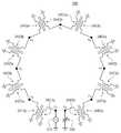
도 2에 도시된 바와 같이, 상기 플라즈마 발생 유닛(300)은 RF 전원(310), 플라즈마 챔버(320), 다수의 전자장 인가기(341 내지 348) 및 리액턴스 소자(350)를 포함할 수 있다.2, the
상기 RF 전원(310)은 RF 신호를 제공할 수 있다. 상기 전자장 인가기(341 내지 348)는 상기 RF 신호를 공급받아 전자장을 유도할 수 있다. 상기 플라즈마 챔버(320)는 상기 전자장 인가기(341 내지 348)가 배치되며, 플라즈마가 생성되는 공간을 제공할 수 있다. 상기 리액턴스 소자(350)는 상기 전자장 인가기(348)의 접지단에 연결될 수 있다.The
일 실시예에 따르면, 상기 RF 전원(310)은 RF 신호를 생성하여 전자장 인가기(341 내지 348)로 출력할 수 있다. 상기 RF 전원(310)은 RF 신호를 통해 플라즈마 챔버(320)에 고주파 전력을 전달할 수 있다. 본 발명의 일 실시예에 따르면, 상기 RF 전원(310)은 정현파 형태의 RF 신호를 생성하여 출력할 수 있으나, 상기 RF 신호는 이에 제한되지 않고 구형파, 삼각파, 톱니파, 펄스파 등 다양한 파형을 가질 수 있다.According to one embodiment, the
상기 플라즈마 챔버(320)는 소스 가스를 주입받고, 주입된 가스가 플라즈마 상태로 변화하는 공간을 제공할 수 있다. 일 실시예에 따르면, 상기 플라즈마 챔버(320)는 RF 신호를 통해 전달되는 고주파 전력을 이용하여 챔버에 주입되는 가스를 플라즈마 상태로 여기시키는 공간을 제공할 수 있다.The
일 실시예에 따르면, 상기 플라즈마 챔버(320)는 외벽이 다각형의 단면을 갖도록 형성될 수 있다. 예를 들어, 도 2에 도시된 바와 같이, 상기 플라즈마 챔버(320)는 단면이 팔각형인 외벽을 가질 수 있으나, 단면의 형상은 이에 제한되지 않는다.According to one embodiment, the
본 발명의 일 실시예에 따르면, 상기 플라즈마 챔버(320)의 외벽 단면 형상은 챔버에 배치되는 전자장 인가기의 개수에 따라 결정될 수 있다. 예를 들어, 도 2에 도시된 바와 같이, 플라즈마 챔버(320)의 외벽 단면이 팔각형인 경우, 상기 팔각형의 각 변에 해당되는 측벽에 상기 전자장 인가기가 배치될 수 있다.According to an embodiment of the present invention, the outer wall cross-sectional shape of the
이와 같이, 상기 플라즈마 챔버(320)의 외벽 단면이 다각형인 경우, 상기 다각형의 변의 개수는 전자장 인가기의 개수와 일치할 수 있다. 또한, 도 2에 도시된 바와 같이, 상기 플라즈마 챔버(320)의 내벽은 단면이 원형일 수 있으나, 내벽 단면의 형상은 이에 제한되지 않는다.When the outer wall of the
상기 전자장 인가기(341 내지 348)는 플라즈마 챔버(320)에 배치되며, RF 전원(310)으로부터 RF 신호를 공급받아 챔버에 전자장을 유도할 수 있다.The electromagnetic
일 실시예에 따르면, 상기 전자장 인가기(341 내지 348)는 플라즈마 챔버(320)의 둘레에 형성된 절연 루프를 통해 챔버에 배치될 수 있다.According to one embodiment, the electromagnetic
예를 들어, 도 2에 도시된 바와 같이, 상기 플라즈마 챔버(320)의 둘레에는 다수의 절연 루프(331 내지 338)가 구비될 수 있다. 상기 절연 루프(331 내지 338)는 절연체로 만들어지며, 일 예로 쿼츠 또는 세라믹으로 만들어질 수 있으나 이에 제한되지는 않는다.For example, as shown in FIG. 2, a plurality of insulating
상기 다수의 절연 루프(331 내지 338)는 플라즈마 챔버(320)의 둘레를 따라 형성될 수 있다. 예를 들어, 도 2에 도시된 바와 같이, 상기 다수의 절연 루프(331 내지 338)는 플라즈마 챔버(320)의 외벽에 일정 간격마다 설치될 수 있다. 도 2에 도시된 플라즈마 발생 유닛(300)은 8 개의 절연 루프(331 내지 338)를 포함하나, 실시예에 따라 절연 루프의 개수는 변경될 수 있다.The plurality of insulating
상기 절연 루프(331 내지 338)는 플라즈마 챔버(320)의 외벽과 함께 폐루프를 형성할 수 있다. 예를 들어, 도 2에 도시된 바와 같이, 상기 절연 루프(331 내지 338)는 'ㄷ' 또는 'U'자 모양으로 형성될 수 있으며, 플라즈마 챔버(320)의 외벽에 설치되는 경우 폐루프를 형성할 수 있다.The insulating
상기 전자장 인가기(341 내지 348)는 상기 절연 루프(331 내지 338)에 설치될 수 있다.The electromagnetic
도 3은 본 발명의 일 실시예에 따른 전자장 인가기(341)의 정면 모습을 나타내는 예시적인 도면이다.3 is an exemplary diagram illustrating a front view of an
상기 전자장 인가기(341)는 제 1 코어(3411), 제 2 코어(3412), 1차 코일(3413a) 및 2차 코일(3413b)을 포함할 수 있다. 상기 제 1 코어(3411)는 자성체로 구성되며, 절연 루프(331)의 제 1 부분을 감쌀 수 있다. 상기 제 2 코어(3412) 역시 자성체로 구성되며, 절연 루프(331)의 제 2 부분을 감쌀 수 있다. 상기 1차 코일(3413a)은 제 1 코어(3411)와 제 2 코어(3412)의 일부분에 감길 수 있다. 상기 2차 코일(3413b)은 제 1 코어(3411)와 제 2 코어(3412)의 타부분에 감길 수 있다.The electromagnetic
도 3에 도시된 바와 같이, 일 실시예에 따르면, 상기 제 1 코어(3411)는 절연 루프(331)의 제 1 부분 중 상반부를 감싸는 제 1 상측 코어(3411a), 및 절연 루프(331)의 제 1 부분 중 하반부를 감싸는 제 1 하측 코어(3411b)를 포함할 수 있다.3, the
또한, 상기 제 2 코어(3412)는 절연 루프(331)의 제 2 부분 중 상반부를 감싸는 제 2 상측 코어(3412a), 및 절연 루프(331)의 제 2 부분 중 하반부를 감싸는 제 2 하측 코어(3412b)를 포함할 수 있다.The
도 3에 도시된 바와 같이, 상기 제 1 코어(3411)와 상기 제 2 코어(3412)는 서로 맞닿아 있을 수 있으며, 상기 1차 코일(3413a)과 상기 2차 코일(3413b)은 제 1 및 제 2 코어(3411, 3412)의 서로 맞닿아 있는 부분에 감길 수 있다.3, the
이와 같이, 1차 코일(3413a)과 2차 코일(3413b)이 코어를 공유한 채 서로 분리되어 감김으로써, 상기 1차 코일(3413a)과 상기 2차 코일(3413b)은 상호 유도 결합될 수 있다.Thus, the
일 실시예에 따르면, 각각의 전자장 인가기에 포함된 코일들, 예컨대 1차 코일(3413a)과 2차 코일(3413b)은 권선 수가 동일할 수 있다. 다시 말해, 상호 유도 결합된 두 코일은 그 권선 비가 1:1일 수 있다.According to one embodiment, the coils included in each of the electromagnetic field application units, e.g., the
일 실시예에 따르면, 도 3에 도시된 바와 같이, 상기 제 1 상측 코어(3411a)와 상기 제 2 상측 코어(3411b) 사이에는 절연체(3414)가 삽입될 수 있다. 마찬가지로, 상기 제 2 상측 코어(3412a)와 상기 제 2 하측 코어(3412b) 사이에도 절연체(3414)가 삽입될 수 있다.According to one embodiment, as shown in FIG. 3, an
상기 절연체는 절연 물질로 만들어진 테잎일 수 있으며, 이 경우 상측 코어와 하측 코어 간의 간격(d1, d2)을 조절하기 위해 한 장 또는 그 이상의 절연 테잎이 상측 코어와 하측 코어 사이에 부착될 수 있다.The insulator may be a tape made of an insulating material, in which case one or more insulating tapes may be attached between the upper core and the lower core to control the spacing d1 , d2 between the upper and lower cores have.
상기 상측 코어와 상기 하측 코어 간의 간격(d1, d2)이 커질수록 코어와 코일 간의 결합계수가 감소하여 인덕턴스가 작아질 수 있다. 인덕턴스가 작아질수록 전자장 인가기의 임피던스는 작아지므로, 플라즈마 발생 유닛(300)을 이용하여 생성할 플라즈마의 밀도에 따라 상기 간격을 결정할 수 있다.As the distance (d1 , d2 ) between the upper core and the lower core increases, the coupling coefficient between the core and the coil decreases and the inductance decreases. As the inductance becomes smaller, the impedance of the electromagnetic field applying unit becomes smaller. Therefore, the interval can be determined according to the density of the plasma to be generated using the
도 3에 도시된 실시예는 각각의 코어(3411, 3412)가 두 개의 서브 코어들(3411a와 3411b, 3412a와 3412b)로 반분되어 구성되나, 실시예에 따라 각각의 코어는 일체로 형성될 수도 있으며, 나아가 상기 제 1 및 제 2 코어(3411, 3412) 전체가 일체로 형성될 수도 있다.Although the embodiment shown in FIG. 3 is configured such that each
또한, 도 3에 도시된 실시예는 도 2에 도시된 다수의 전자장 인가기(341 내지 348) 중 하나에 대해서만 설명하였으나, 나머지 전자장 인가기들도 모두 동일하게 구성될 수 있다.In addition, although the embodiment shown in FIG. 3 has been described for only one of the plurality of electromagnetic
도 4는 본 발명의 일 실시예에 따른 플라즈마 발생 유닛(300)의 등가 회로도다.4 is an equivalent circuit diagram of the
도 4에 도시된 바와 같이, 각각의 전자장 인가기에 포함된 1차 코일 및 2차 코일은 상호 유도 결합되어 있으며 두 코일의 권선 비는 1:1이므로, 각각의 전자장 인가기는 1:1 전압 변압기(voltage transformer)에 대응할 수 있다.As shown in FIG. 4, the primary and secondary coils included in each of the electromagnetic field applying units are mutually inductively coupled, and the coil ratio of the two coils is 1: 1, so that each of the electromagnetic field applying units has a 1: 1 voltage transformer voltage transformer.
일 실시예에 따르면, 상기 다수의 전자장 인가기(341 내지 348)는 서로 직렬로 연결될 수 있다.According to one embodiment, the plurality of electromagnetic
다수의 전자장 인가기(341 내지 348)가 서로 직렬로 연결되어 있음에도 불구하고, 각각의 전자장 인가기에 포함된 코일들이 상호 유도 결합되어 1:1 전압 변압기를 구현하므로, 플라즈마 발생 유닛(300)의 각 노드(n1 내지 n9)에 인가되는 전압은 크기가 모두 동일할 수 있다.Although the plurality of electromagnetic
그 결과, 각각의 전자장 인가기에 의해 유도되는 전자장의 세기는 모두 동일하게 되며, 챔버에 생성되는 플라즈마의 밀도 역시 챔버 둘레에 걸쳐 균일하게 분포할 수 있다.As a result, the intensities of the electromagnetic fields induced by the respective electromagnetic field applying units become equal, and the density of the plasma generated in the chamber can also be uniformly distributed around the chamber.
도 5는 본 발명의 다른 실시예에 따른 플라즈마 발생 유닛(300)의 등가 회로도다.5 is an equivalent circuit diagram of the
도 5에 도시된 바와 같이, 상기 플라즈마 발생 유닛(300)은 위상 조절기(360)를 더 포함할 수 있다. 상기 위상 조절기(360)는 RF 전원(310)과 다수의 전자장 인가기(341 내지 348) 간의 노드들(n1 내지 n8)에 구비되어 각 노드에서 RF신호의 위상을 동일하게 고정시킬 수 있다.As shown in FIG. 5, the
이 실시예에 따르면, 플라즈마 발생 유닛(300)의 각 노드에 인가되는 전압은 진폭 뿐만 아니라 위상도 동일하게 조절될 수 있다.According to this embodiment, the voltage applied to each node of the
도 6은 본 발명의 또 다른 실시예에 따른 플라즈마 발생 유닛(300)의 등가 회로도다.6 is an equivalent circuit diagram of the
도 6에 도시된 바와 같이, 상기 플라즈마 발생 유닛(300)은 분로(shunt) 리액턴스 소자(370)를 더 포함할 수 있다. 상기 분로 리액턴스 소자(370)는 다수의 전자장 인가기(341 내지 348) 간의 노드들(n2 내지 n8)에 연결될 수 있다. 다시 말해, 상기 분로 리액턴스 소자(370)의 일단은 전자장 인가기들 간의 노드(n2 내지 n8)에 연결되고, 타단은 접지될 수 있다.As shown in FIG. 6, the
일 실시예에 따르면, 상기 분로 리액턴스 소자(370)는 용량성 소자인 커패시터일 수 있으며, 그 임피던스는 상호 유도 결합된 코일들 중 2차 코일(L)과 접지단에 연결된 리액턴스 소자(C)의 합성 임피던스의 절반일 수 있다.According to one embodiment, the shunting
이 실시예에 따르면, 상기 분로 리액턴스 소자(370)는 플라즈마 발생 유닛(300)의 전원측 입력단과 접지측 출력단의 전압을 동일하게 만들 수 있다.According to this embodiment, the
본 발명의 일 실시예에 따르면, 상기 리액턴스 소자(350)는 가변 커패시터를 포함할 수 있다. 이 실시예에 따르면, 상기 플라즈마 발생 유닛(300)은 상기 가변 커패시터의 커패시턴스를 조절하여 각 전자장 인가기에서의 전압 강하량을 제어할 수 있다.According to an embodiment of the present invention, the
일 예로, 상기 가변 커패시터의 커패시턴스를 감소시켜 임피던스를 증가시키는 경우, 상기 가변 커패시터에서의 전압 강하량이 증가한 결과 상대적으로 각 전자장 인가기에서의 전압 강하량이 감소하게 된다.For example, when the impedance of the variable capacitor is decreased by decreasing the capacitance of the variable capacitor, the amount of voltage drop at each of the electromagnetic field applying devices is relatively reduced as a result of an increase in the voltage drop amount at the variable capacitor.
다른 예로, 상기 가변 커패시터의 커패시턴스를 증가시켜 임피던스를 감소시키는 경우, 상기 가변 커패시터에서의 전압 강하량이 감소한 결과 상대적으로 각 전자장 인가기에서의 전압 강하량이 증가하게 된다.As another example, when the impedance of the variable capacitor is increased by increasing the capacitance of the variable capacitor, the amount of voltage drop in the variable capacitor is relatively decreased, resulting in an increase in the voltage drop in each of the electromagnetic field applying devices.
따라서, 상기 플라즈마 발생 유닛(300)은 기판 처리 공정 또는 챔버 내 환경 등에 따라 원하는 플라즈마 밀도를 얻기 위해 상기 가변 커패시터의 커패시턴스를 조절하여 전자장 인가기에서의 전압 강하량을 조절할 수 있다.Accordingly, the
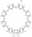
도 7은 본 발명의 또 다른 실시예에 따른 플라즈마 발생 유닛(300)의 평면 모습을 나타내는 예시적인 도면이다.7 is an exemplary diagram showing a plan view of a
도 7에 도시된 실시예는, 각 전자장 인가기에 포함된 제 1 및 제 2 코어(3411, 3412)가 서로 맞붙어 있어 1차 및 2차 코일(3413a, 3413b)이 코어들의 서로 맞붙어 있는 부분에 감겨 있는 도 2에 도시된 실시예와 달리, 상기 제 1 및 제 2 코어가 서로 이격되어 있으며 각 코어의 일부분에 1차 코일이 감겨 있고 각 코어의 타부분에 2차 코일이 감겨 있다.In the embodiment shown in Fig. 7, the first and
도 8은 본 발명의 또 다른 실시예에 따른 전자장 인가기(341)의 정면 모습을 나타내는 예시적인 도면이다.8 is an exemplary diagram showing a front view of an electromagnetic
도 8에 도시된 바와 같이, 본 발명의 또 다른 실시예에 따른 전자장 인가기(341)는 제 1 코어(3411)와 제 2 코어(3412)가 서로 이격되어 있으며, 각 코어의 일부분에는 1차 코일(3413a, 3413c)이 감겨 있고, 타부분에는 2차 코일(3413b, 3413d)이 감겨 있을 수 있다.8, in the electromagnetic
상기 제 1 및 제 2 코어(3411, 3412)는 각각 별도의 폐루프를 형성하며, 1차 코일(3413a, 3413c)과 2차 코일(3413b, 3413d)은 하나의 코어를 공유하여 상호 유도 결합된다.The first and
각 코일의 권선 수는 모두 동일할 수 있으며, 이 경우 1차 코일(3413a, 3413c)과 2차 코일(3413b, 3413d) 간의 권선 비는 1:1이 되어, 각각의 코어와 그에 감긴 코일들은 1:1의 전압 변압기를 구현할 수 있다.In this case, the ratio of turns between the
도 9는 본 발명의 또 다른 실시예에 따른 플라즈마 발생 유닛(300)의 등가 회로도다.9 is an equivalent circuit diagram of a
도 9에 도시된 바와 같이, 전자장 인가기(341 내지 348)의 각 코어와 그에 감긴 코일들은 상호 유도 결합 회로를 구성하여 1:1 전압 변압기에 대응할 수 있다.As shown in FIG. 9, each core of the electromagnetic
그 결과, 플라즈마 발생 유닛(300)의 각 노드(n1 내지 n17)에 인가되는 전압의 크기는 모두 동일하게 조절될 수 있다.As a result, the magnitude of the voltage applied to each node (n1 to n17 ) of the
실시예에 따라, 노드(n1 내지 n16)에는 위상 조절기(360)가 더 구비되어, 각 노드에서 RF 신호의 위상도 동일하게 고정될 수 있다.According to the embodiment, the nodes n1 to n16 are further provided with a
실시예에 따라, 노드(n2 내지 n16)에는 분로 리액턴스 소자(370)가 연결될 수 있으며, 상기 분로 리액턴스 소자(370)의 타단은 접지될 수 있다. 상기 분로 리액턴스 소자(370)는 커패시터일 수 있으며, 그 임피던스는 상호 유도 결합된 코일들 중 2차 코일(L)과 리액턴스 소자(C)의 합성 임피던스의 절반으로 조절될 수 있다.According to the embodiment, the
다시 도 8을 참조하면, 전술한 도 3에 도시된 실시예와 마찬가지로, 상기 제 1 코어(3411)는 폐루프의 절반부를 형성하는 제 1 서브 코어, 예컨대 제 1 상측 코어(3411a); 및 폐루프의 나머지 절반부를 형성하는 제 2 서브 코어, 예컨대 제 1 하측 코어(3411b)를 포함할 수 있다. 또한, 상기 제 2 코어(3412)는 폐루프의 절반부를 형성하는 제 3 서브 코어, 예컨대 제 2 상측 코어(3412a); 및 폐루프의 나머지 절반부를 형성하는 제 4 서브 코어, 예컨대 제 2 하측 코어(3412b)를 포함할 수 있다.Referring again to FIG. 8, as in the embodiment shown in FIG. 3, the
실시예에 따라, 상기 제 1 서브 코어와 상기 제 2 서브 코어 사이에는 절연체(3414)가 삽입될 수 있으며, 제 3 서브 코어와 제 4 서브 코어 사이에도 절연체(3414)가 삽입될 수 있다.According to an embodiment, an
이상에서 실시예를 통해 본 발명을 설명하였으나, 위 실시예는 단지 본 발명의 사상을 설명하기 위한 것으로 이에 한정되지 않는다. 통상의 기술자는 전술한 실시예에 다양한 변형이 가해질 수 있음을 이해할 것이다. 본 발명의 범위는 첨부된 특허청구범위의 해석을 통해서만 정해진다.While the present invention has been described with reference to the exemplary embodiments, it is to be understood that the invention is not limited to the disclosed exemplary embodiments. Those skilled in the art will appreciate that various modifications may be made to the embodiments described above. The scope of the present invention is defined only by the interpretation of the appended claims.
10: 기판 처리 장치
100: 공정 유닛
200: 배기 유닛
300: 플라즈마 발생 유닛
310: RF 전원
320: 플라즈마 챔버
330: 절연 루프
340: 전자장 인가기
350: 리액턴스 소자10: substrate processing apparatus
100: Process unit
200: Exhaust unit
300: Plasma generating unit
310: RF power
320: Plasma chamber
330: Isolation Loop
340:
350: reactance element
Claims (21)
Translated fromKorean상기 RF 신호를 공급받아 전자장을 유도하는 다수의 전자장 인가기; 및
상기 전자장 인가기의 접지단에 연결되는 리액턴스 소자를 포함하며,
각각의 전자장 인가기는 유도 결합된 다수의 코일을 포함하고,
상기 전자장 인가기는:
자성체로 구성된 코어;
상기 코어의 일부분에 감긴 제 1 코일; 및
상기 코어의 타부분에 감긴 제 2 코일;
을 포함하는 플라즈마 생성 장치.An RF power supply for supplying an RF signal;
A plurality of electromagnetic field applying units for receiving the RF signal to induce an electromagnetic field; And
And a reactance element connected to a ground terminal of the electromagnetic field applying device,
Each electromagnetic field applicator comprises a plurality of inductively coupled coils,
The electromagnetic field applicator comprises:
A core composed of a magnetic body;
A first coil wound around a portion of the core; And
A second coil wound around another portion of the core;
And a plasma generator.
상기 다수의 전자장 인가기는 서로 직렬로 연결되는 플라즈마 생성 장치.The method according to claim 1,
Wherein the plurality of electromagnetic field applying units are connected in series with each other.
각각의 전자장 인가기에 포함된 코일들은 권선 수가 동일한 플라즈마 생성 장치.The method according to claim 1,
Wherein the coils included in each of the electromagnetic field applying units have the same number of windings.
상기 코어는:
제 1 폐루프를 형성하는 제 1 코어; 및
제 2 폐루프를 형성하는 제 2 코어;
를 포함하는 플라즈마 생성 장치.The method according to claim 1,
Said core comprising:
A first core forming a first closed loop; And
A second core forming a second closed loop;
And a plasma generator.
상기 제 1 코어는:
상기 제 1 폐루프의 절반부를 형성하는 제 1 서브 코어; 및
상기 제 1 폐루프의 나머지 절반부를 형성하는 제 2 서브 코어를 포함하고,
상기 제 2 코어는:
상기 제 2 폐루프의 절반부를 형성하는 제 3 서브 코어; 및
상기 제 2 폐루프의 나머지 절반부를 형성하는 제 4 서브 코어를 포함하는 플라즈마 생성 장치.6. The method of claim 5,
The first core comprising:
A first sub-core forming a half of the first closed loop; And
And a second sub-core forming the other half of the first closed loop,
Said second core comprising:
A third sub-core forming a half of the second closed loop; And
And a fourth sub-core forming the other half of the second closed loop.
상기 제 1 서브 코어와 상기 제 2 서브 코어 사이, 그리고 상기 제 3 서브 코어와 상기 제 4 서브 코어 사이에는 절연체가 삽입되는 플라즈마 생성 장치.The method according to claim 6,
An insulator is inserted between the first sub-core and the second sub-core, and between the third sub-core and the fourth sub-core.
상기 RF 신호를 공급받아 전자장을 유도하는 다수의 전자장 인가기; 및
상기 전자장 인가기의 접지단에 연결되는 리액턴스 소자를 포함하며,
각각의 전자장 인가기는 유도 결합된 다수의 코일을 포함하고,
상기 RF 전원과 상기 다수의 전자장 인가기 간의 노드들에 구비되어 각 노드에서 상기 RF 신호의 위상을 동일하게 고정시키는 위상 조절기를 포함하는 플라즈마 생성 장치.An RF power supply for supplying an RF signal;
A plurality of electromagnetic field applying units for receiving the RF signal to induce an electromagnetic field; And
And a reactance element connected to a ground terminal of the electromagnetic field applying device,
Each electromagnetic field applicator comprises a plurality of inductively coupled coils,
And a phase adjuster provided at nodes between the RF power source and the plurality of electromagnetic field applying units to fix the phase of the RF signal equally to each node.
상기 RF 신호를 공급받아 전자장을 유도하는 다수의 전자장 인가기; 및
상기 전자장 인가기의 접지단에 연결되는 리액턴스 소자를 포함하며,
각각의 전자장 인가기는 유도 결합된 다수의 코일을 포함하고,
상기 다수의 전자장 인가기 간의 노드들에 연결된 분로(shunt) 리액턴스 소자를 포함하는 플라즈마 생성 장치.An RF power supply for supplying an RF signal;
A plurality of electromagnetic field applying units for receiving the RF signal to induce an electromagnetic field; And
And a reactance element connected to a ground terminal of the electromagnetic field applying device,
Each electromagnetic field applicator comprises a plurality of inductively coupled coils,
And a shunt reactance element coupled to the nodes between the plurality of electromagnetic field application devices.
상기 분로 리액턴스 소자의 임피던스는 상기 상호 유도 결합된 코일들 중 2차 코일과 상기 리액턴스 소자의 합성 임피던스의 절반인 플라즈마 생성 장치.10. The method of claim 9,
Wherein an impedance of the shunt reactance element is half of a combined impedance of the secondary coil and the reactance element of the mutually inductively coupled coils.
상기 리액턴스 소자는 가변 커패시터를 포함하는 플라즈마 생성 장치.The method according to claim 1,
And the reactance element includes a variable capacitor.
플라즈마를 발생시켜 상기 공정 유닛으로 플라즈마를 제공하는 플라즈마 발생 유닛; 및
상기 공정 유닛 내부의 가스 및 반응 부산물을 배출하는 배기 유닛을 포함하며,
상기 플라즈마 발생 유닛은:
RF 신호를 공급하는 RF 전원;
상기 RF 신호를 공급받아 전자장을 유도하는 다수의 전자장 인가기;
상기 전자장 인가기가 배치되며, 플라즈마가 생성되는 공간을 제공하는 플라즈마 챔버; 및
상기 전자장 인가기의 접지단에 연결되는 리액턴스 소자를 포함하며,
각각의 전자장 인가기는 유도 결합된 다수의 코일을 포함하며,
상기 플라즈마 챔버는 둘레에 다수의 절연 루프를 가지며,
상기 전자장 인가기는:
자성체로 구성되며, 상기 절연 루프의 제 1 부분을 감싸는 제 1 코어;
상기 자성체로 구성되며, 상기 절연 루프의 제 2 부분을 감싸는 제 2 코어;
상기 제 1 코어와 상기 제 2 코어의 일부분에 감긴 1차 코일; 및
상기 제 1 코어와 상기 제 2 코어의 타부분에 감긴 2차 코일;
을 포함하는 기판 처리 장치. 기판 처리 장치.A processing unit including a processing chamber in which a substrate is disposed, the processing unit providing a space in which the processing is performed;
A plasma generating unit for generating a plasma to supply a plasma to the processing unit; And
And an exhaust unit for exhausting gas and reaction by-products inside the processing unit,
The plasma generating unit includes:
An RF power supply for supplying an RF signal;
A plurality of electromagnetic field applying units for receiving the RF signal to induce an electromagnetic field;
A plasma chamber in which the electromagnetic field applicator is disposed and which provides a space in which plasma is generated; And
And a reactance element connected to a ground terminal of the electromagnetic field applying device,
Each electromagnetic field applicator comprises a plurality of inductively coupled coils,
The plasma chamber having a plurality of insulating loops around it,
The electromagnetic field applicator comprises:
A first core comprising a magnetic body and surrounding a first portion of the insulating loop;
A second core composed of the magnetic body, the second core surrounding the second portion of the insulating loop;
A primary coil wound around the first core and a portion of the second core; And
A secondary coil wound around the first core and the other portion of the second core;
And the substrate processing apparatus. / RTI >
상기 다수의 전자장 인가기는 서로 직렬로 연결되는 기판 처리 장치.13. The method of claim 12,
Wherein the plurality of electromagnetic field applying units are connected in series with each other.
각각의 전자장 인가기에 포함된 코일들은 권선 수가 동일한 기판 처리 장치.13. The method of claim 12,
Wherein the coils included in each of the electromagnetic field applying units have the same number of windings.
상기 제 1 코어는:
상기 절연 루프의 제 1 부분 중 상반부를 감싸는 제 1 상측 코어;
상기 절연 루프의 제 1 부분 중 하반부를 감싸는 제 1 하측 코어를 포함하고,
상기 제 2 코어는:
상기 절연 루프의 제 2 부분 중 상반부를 감싸는 제 2 상측 코어; 및
상기 절연 루프의 제 2 부분 중 하반부를 감싸는 제 2 하측 코어를 포함하는 기판 처리 장치.13. The method of claim 12,
The first core comprising:
A first upper core surrounding the upper half of the first portion of the insulating loop;
And a first lower core surrounding a lower half of the first portion of the insulating loop,
Said second core comprising:
A second upper core surrounding the upper half of the second portion of the insulating loop; And
And a second lower core surrounding the lower half of the second portion of the insulating loop.
상기 제 1 상측 코어와 상기 제 1 하측 코어 사이, 그리고 상기 제 2 상측 코어와 상기 제 2 하측 코어 사이에는 절연체가 삽입되는 기판 처리 장치.17. The method of claim 16,
Wherein an insulator is inserted between the first upper core and the first lower core, and between the second upper core and the second lower core.
플라즈마를 발생시켜 상기 공정 유닛으로 플라즈마를 제공하는 플라즈마 발생 유닛; 및
상기 공정 유닛 내부의 가스 및 반응 부산물을 배출하는 배기 유닛을 포함하며,
상기 플라즈마 발생 유닛은:
RF 신호를 공급하는 RF 전원;
상기 RF 신호를 공급받아 전자장을 유도하는 다수의 전자장 인가기;
상기 전자장 인가기가 배치되며, 플라즈마가 생성되는 공간을 제공하는 플라즈마 챔버; 및
상기 전자장 인가기의 접지단에 연결되는 리액턴스 소자를 포함하며,
각각의 전자장 인가기는 유도 결합된 다수의 코일을 포함하며,
상기 플라즈마 발생 유닛은:
상기 RF 전원과 상기 다수의 전자장 인가기 간의 노드들에 구비되어 각 노드에서 상기 RF 신호의 위상을 동일하게 고정시키는 위상 조절기를 더 포함하는 기판 처리 장치.A processing unit including a processing chamber in which a substrate is disposed, the processing unit providing a space in which the processing is performed;
A plasma generating unit for generating a plasma to supply a plasma to the processing unit; And
And an exhaust unit for exhausting gas and reaction by-products inside the processing unit,
The plasma generating unit includes:
An RF power supply for supplying an RF signal;
A plurality of electromagnetic field applying units for receiving the RF signal to induce an electromagnetic field;
A plasma chamber in which the electromagnetic field applicator is disposed and which provides a space in which plasma is generated; And
And a reactance element connected to a ground terminal of the electromagnetic field applying device,
Each electromagnetic field applicator comprises a plurality of inductively coupled coils,
The plasma generating unit includes:
And a phase adjuster provided at nodes between the RF power source and the plurality of electromagnetic field applying units to fix the phase of the RF signal at each node equally.
플라즈마를 발생시켜 상기 공정 유닛으로 플라즈마를 제공하는 플라즈마 발생 유닛; 및
상기 공정 유닛 내부의 가스 및 반응 부산물을 배출하는 배기 유닛을 포함하며,
상기 플라즈마 발생 유닛은:
RF 신호를 공급하는 RF 전원;
상기 RF 신호를 공급받아 전자장을 유도하는 다수의 전자장 인가기;
상기 전자장 인가기가 배치되며, 플라즈마가 생성되는 공간을 제공하는 플라즈마 챔버; 및
상기 전자장 인가기의 접지단에 연결되는 리액턴스 소자를 포함하며,
각각의 전자장 인가기는 유도 결합된 다수의 코일을 포함하며,
상기 플라즈마 발생 유닛은:
상기 다수의 전자장 인가기 간의 노드들에 연결된 분로 리액턴스 소자를 더 포함하는 기판 처리 장치.A processing unit including a processing chamber in which a substrate is disposed, the processing unit providing a space in which the processing is performed;
A plasma generating unit for generating a plasma to supply a plasma to the processing unit; And
And an exhaust unit for exhausting gas and reaction by-products inside the processing unit,
The plasma generating unit includes:
An RF power supply for supplying an RF signal;
A plurality of electromagnetic field applying units for receiving the RF signal to induce an electromagnetic field;
A plasma chamber in which the electromagnetic field applicator is disposed and which provides a space in which plasma is generated; And
And a reactance element connected to a ground terminal of the electromagnetic field applying device,
Each electromagnetic field applicator comprises a plurality of inductively coupled coils,
The plasma generating unit includes:
And a shunting reactance element coupled to the nodes between the plurality of electromagnetic field application devices.
상기 분로 리액턴스 소자의 임피던스는 상기 상호 유도 결합된 코일들 중 2차 코일과 상기 리액턴스 소자의 합성 임피던스의 절반인 기판 처리 장치.20. The method of claim 19,
Wherein the impedance of the shunted reactance element is half the combined impedance of the secondary coil and the reactance element of the mutually inductively coupled coils.
상기 리액턴스 소자는 가변 커패시터를 포함하는 기판 처리 장치.13. The method of claim 12,
Wherein the reactance element comprises a variable capacitor.
Priority Applications (4)
| Application Number | Priority Date | Filing Date | Title |
|---|---|---|---|
| KR1020130143316AKR101532376B1 (en) | 2013-11-22 | 2013-11-22 | Apparatus for generating plasma using mutual inductive coupling, and apparatus for treating substrate comprising the same |
| US14/516,766US10312060B2 (en) | 2013-11-22 | 2014-10-17 | Plasma generating apparatus using mutual inductive coupling and substrate treating apparatus comprising the same |
| TW103136524ATW201521523A (en) | 2013-11-22 | 2014-10-22 | Plasma generating apparatus using mutual inductive coupling and substrate treating apparatus comprising the same |
| JP2014230447AJP6071978B2 (en) | 2013-11-22 | 2014-11-13 | Plasma generating apparatus using mutual inductive coupling and substrate processing apparatus including the same |
Applications Claiming Priority (1)
| Application Number | Priority Date | Filing Date | Title |
|---|---|---|---|
| KR1020130143316AKR101532376B1 (en) | 2013-11-22 | 2013-11-22 | Apparatus for generating plasma using mutual inductive coupling, and apparatus for treating substrate comprising the same |
Publications (2)
| Publication Number | Publication Date |
|---|---|
| KR20150059561A KR20150059561A (en) | 2015-06-01 |
| KR101532376B1true KR101532376B1 (en) | 2015-07-01 |
Family
ID=53181638
Family Applications (1)
| Application Number | Title | Priority Date | Filing Date |
|---|---|---|---|
| KR1020130143316AExpired - Fee RelatedKR101532376B1 (en) | 2013-11-22 | 2013-11-22 | Apparatus for generating plasma using mutual inductive coupling, and apparatus for treating substrate comprising the same |
Country Status (4)
| Country | Link |
|---|---|
| US (1) | US10312060B2 (en) |
| JP (1) | JP6071978B2 (en) |
| KR (1) | KR101532376B1 (en) |
| TW (1) | TW201521523A (en) |
Citations (2)
| Publication number | Priority date | Publication date | Assignee | Title |
|---|---|---|---|---|
| JP2004533090A (en)* | 2001-03-30 | 2004-10-28 | ラム リサーチ コーポレーション | Induction plasma processing apparatus including current sensor for plasma excitation coil |
| KR20060108089A (en)* | 2005-04-12 | 2006-10-17 | 한양대학교 산학협력단 | Inductively Coupled Plasma Generator Using Magnetic Core |
Family Cites Families (20)
| Publication number | Priority date | Publication date | Assignee | Title |
|---|---|---|---|---|
| JP3311391B2 (en)* | 1991-09-13 | 2002-08-05 | ヴィエルティー コーポレーション | Leakage inductance reducing transformer, high frequency circuit and power converter using the same, and method of reducing leakage inductance in transformer |
| JPH065448A (en)* | 1992-06-22 | 1994-01-14 | Matsushita Electric Ind Co Ltd | Choke coil and power supply |
| US5907221A (en) | 1995-08-16 | 1999-05-25 | Applied Materials, Inc. | Inductively coupled plasma reactor with an inductive coil antenna having independent loops |
| US7166816B1 (en) | 1997-06-26 | 2007-01-23 | Mks Instruments, Inc. | Inductively-coupled torodial plasma source |
| US6273022B1 (en) | 1998-03-14 | 2001-08-14 | Applied Materials, Inc. | Distributed inductively-coupled plasma source |
| US6388382B1 (en)* | 1999-03-09 | 2002-05-14 | Hitachi, Ltd. | Plasma processing apparatus and method |
| US7223676B2 (en) | 2002-06-05 | 2007-05-29 | Applied Materials, Inc. | Very low temperature CVD process with independently variable conformality, stress and composition of the CVD layer |
| US7096819B2 (en)* | 2001-03-30 | 2006-08-29 | Lam Research Corporation | Inductive plasma processor having coil with plural windings and method of controlling plasma density |
| US20030015965A1 (en)* | 2002-08-15 | 2003-01-23 | Valery Godyak | Inductively coupled plasma reactor |
| US8409400B2 (en)* | 2003-05-07 | 2013-04-02 | Gen Co., Ltd. | Inductive plasma chamber having multi discharge tube bridge |
| JP2005285564A (en)* | 2004-03-30 | 2005-10-13 | Mitsui Eng & Shipbuild Co Ltd | Plasma processing equipment |
| KR100720989B1 (en) | 2005-07-15 | 2007-05-28 | 주식회사 뉴파워 프라즈마 | Multi Chamber Plasma Process System |
| KR100689848B1 (en) | 2005-07-22 | 2007-03-08 | 삼성전자주식회사 | Substrate Processing Equipment |
| KR100785164B1 (en) | 2006-02-04 | 2007-12-11 | 위순임 | Multiple output remote plasma generator and substrate processing system having same |
| KR100775593B1 (en) | 2006-04-05 | 2007-11-09 | 세메스 주식회사 | Plasma Source Ashing Device |
| US7837826B2 (en) | 2006-07-18 | 2010-11-23 | Lam Research Corporation | Hybrid RF capacitively and inductively coupled plasma source using multifrequency RF powers and methods of use thereof |
| KR101418438B1 (en)* | 2007-07-10 | 2014-07-14 | 삼성전자주식회사 | Plasma generator |
| US9287096B2 (en) | 2007-09-27 | 2016-03-15 | Lam Research Corporation | Methods and apparatus for a hybrid capacitively-coupled and an inductively-coupled plasma processing system |
| US8088263B1 (en)* | 2009-02-17 | 2012-01-03 | Smith Robert M | Phased magnetic cathode |
| JP5851681B2 (en) | 2009-10-27 | 2016-02-03 | 東京エレクトロン株式会社 | Plasma processing equipment |
- 2013
- 2013-11-22KRKR1020130143316Apatent/KR101532376B1/ennot_activeExpired - Fee Related
- 2014
- 2014-10-17USUS14/516,766patent/US10312060B2/enactiveActive
- 2014-10-22TWTW103136524Apatent/TW201521523A/enunknown
- 2014-11-13JPJP2014230447Apatent/JP6071978B2/ennot_activeExpired - Fee Related
Patent Citations (2)
| Publication number | Priority date | Publication date | Assignee | Title |
|---|---|---|---|---|
| JP2004533090A (en)* | 2001-03-30 | 2004-10-28 | ラム リサーチ コーポレーション | Induction plasma processing apparatus including current sensor for plasma excitation coil |
| KR20060108089A (en)* | 2005-04-12 | 2006-10-17 | 한양대학교 산학협력단 | Inductively Coupled Plasma Generator Using Magnetic Core |
Also Published As
| Publication number | Publication date |
|---|---|
| KR20150059561A (en) | 2015-06-01 |
| JP2015103524A (en) | 2015-06-04 |
| US10312060B2 (en) | 2019-06-04 |
| JP6071978B2 (en) | 2017-02-01 |
| US20150144264A1 (en) | 2015-05-28 |
| TW201521523A (en) | 2015-06-01 |
Similar Documents
| Publication | Publication Date | Title |
|---|---|---|
| KR101660830B1 (en) | Apparatus for generating plasma using dual plasma source and apparatus for treating substrate comprising the same | |
| KR102069923B1 (en) | Plasma processing device and filter unit | |
| JP6218650B2 (en) | Plasma processing equipment | |
| JP6050722B2 (en) | Plasma processing apparatus and filter unit | |
| KR20180119498A (en) | Filter device and plasma processing apparatus | |
| US20140190635A1 (en) | Plasma chamber and apparatus for treating substrate | |
| KR100803794B1 (en) | Inductively coupled plasma source with plasma discharge tube embedded in magnetic core block | |
| CN106711007B (en) | A kind of inductively type plasma processing apparatus | |
| JP2006332055A (en) | Plasma processing chamber, plasma reactor, atmospheric pressure plasma processing system and plasma processing system | |
| JP6138581B2 (en) | Plasma processing equipment | |
| KR100805557B1 (en) | Inductively Coupled Plasma Sources with Multiple Magnetic Cores | |
| KR101533684B1 (en) | Compound plasma reactor | |
| KR101649947B1 (en) | Apparatus for generating plasma using dual plasma source and apparatus for treating substrate comprising the same | |
| WO2014110237A1 (en) | Inductively coupled plasma source | |
| KR101532376B1 (en) | Apparatus for generating plasma using mutual inductive coupling, and apparatus for treating substrate comprising the same | |
| KR101507953B1 (en) | Apparatus for generating plasma using electromagnetic field applicator and apparatus for treating substrate comprising the same | |
| KR100743842B1 (en) | Plasma reactor with plasma chamber coupled to the flux channel | |
| KR101680707B1 (en) | Transformer coupled plasma generator having first winding to ignite and sustain a plasma | |
| KR102407388B1 (en) | Antenna structure for generating inductively coupled plasma |
Legal Events
| Date | Code | Title | Description |
|---|---|---|---|
| PA0109 | Patent application | St.27 status event code:A-0-1-A10-A12-nap-PA0109 | |
| PA0201 | Request for examination | St.27 status event code:A-1-2-D10-D11-exm-PA0201 | |
| PE0902 | Notice of grounds for rejection | St.27 status event code:A-1-2-D10-D21-exm-PE0902 | |
| E13-X000 | Pre-grant limitation requested | St.27 status event code:A-2-3-E10-E13-lim-X000 | |
| P11-X000 | Amendment of application requested | St.27 status event code:A-2-2-P10-P11-nap-X000 | |
| P13-X000 | Application amended | St.27 status event code:A-2-2-P10-P13-nap-X000 | |
| R17-X000 | Change to representative recorded | St.27 status event code:A-3-3-R10-R17-oth-X000 | |
| PG1501 | Laying open of application | St.27 status event code:A-1-1-Q10-Q12-nap-PG1501 | |
| E701 | Decision to grant or registration of patent right | ||
| PE0701 | Decision of registration | St.27 status event code:A-1-2-D10-D22-exm-PE0701 | |
| GRNT | Written decision to grant | ||
| PR0701 | Registration of establishment | St.27 status event code:A-2-4-F10-F11-exm-PR0701 | |
| PR1002 | Payment of registration fee | Fee payment year number:1 St.27 status event code:A-2-2-U10-U11-oth-PR1002 | |
| PG1601 | Publication of registration | St.27 status event code:A-4-4-Q10-Q13-nap-PG1601 | |
| PN2301 | Change of applicant | St.27 status event code:A-5-5-R10-R11-asn-PN2301 St.27 status event code:A-5-5-R10-R13-asn-PN2301 | |
| FPAY | Annual fee payment | Payment date:20180402 Year of fee payment:4 | |
| PR1001 | Payment of annual fee | Fee payment year number:4 St.27 status event code:A-4-4-U10-U11-oth-PR1001 | |
| FPAY | Annual fee payment | Payment date:20190329 Year of fee payment:5 | |
| PR1001 | Payment of annual fee | Fee payment year number:5 St.27 status event code:A-4-4-U10-U11-oth-PR1001 | |
| PN2301 | Change of applicant | St.27 status event code:A-5-5-R10-R11-asn-PN2301 St.27 status event code:A-5-5-R10-R13-asn-PN2301 | |
| PR1001 | Payment of annual fee | Fee payment year number:6 St.27 status event code:A-4-4-U10-U11-oth-PR1001 | |
| PN2301 | Change of applicant | St.27 status event code:A-5-5-R10-R11-asn-PN2301 | |
| PN2301 | Change of applicant | St.27 status event code:A-5-5-R10-R14-asn-PN2301 | |
| PR1001 | Payment of annual fee | Fee payment year number:7 St.27 status event code:A-4-4-U10-U11-oth-PR1001 | |
| PC1903 | Unpaid annual fee | Not in force date:20220624 Payment event data comment text:Termination Category : DEFAULT_OF_REGISTRATION_FEE St.27 status event code:A-4-4-U10-U13-oth-PC1903 | |
| PC1903 | Unpaid annual fee | Ip right cessation event data comment text:Termination Category : DEFAULT_OF_REGISTRATION_FEE Not in force date:20220624 St.27 status event code:N-4-6-H10-H13-oth-PC1903 | |
| P22-X000 | Classification modified | St.27 status event code:A-4-4-P10-P22-nap-X000 | |
| R18-X000 | Changes to party contact information recorded | St.27 status event code:A-5-5-R10-R18-oth-X000 | |
| PN2301 | Change of applicant | St.27 status event code:A-5-5-R10-R11-asn-PN2301 St.27 status event code:A-5-5-R10-R13-asn-PN2301 |