KR101530143B1 - Method for fabricating sensor - Google Patents
Method for fabricating sensorDownload PDFInfo
- Publication number
- KR101530143B1 KR101530143B1KR1020137035100AKR20137035100AKR101530143B1KR 101530143 B1KR101530143 B1KR 101530143B1KR 1020137035100 AKR1020137035100 AKR 1020137035100AKR 20137035100 AKR20137035100 AKR 20137035100AKR 101530143 B1KR101530143 B1KR 101530143B1
- Authority
- KR
- South Korea
- Prior art keywords
- pattern
- layer
- electrode
- photoresist
- gate
- Prior art date
- Legal status (The legal status is an assumption and is not a legal conclusion. Google has not performed a legal analysis and makes no representation as to the accuracy of the status listed.)
- Active
Links
- 238000000034methodMethods0.000titleclaimsabstractdescription44
- 239000000758substrateSubstances0.000claimsabstractdescription38
- 238000000059patterningMethods0.000claimsabstractdescription34
- 238000004519manufacturing processMethods0.000claimsabstractdescription31
- 238000002161passivationMethods0.000claimsabstractdescription23
- 239000000463materialSubstances0.000claimsdescription24
- 229920002120photoresistant polymerPolymers0.000claimsdescription18
- 239000004065semiconductorSubstances0.000claimsdescription17
- 238000000151depositionMethods0.000claimsdescription12
- 238000005530etchingMethods0.000claimsdescription8
- 229910052751metalInorganic materials0.000claimsdescription7
- 239000002184metalSubstances0.000claimsdescription7
- 239000004020conductorSubstances0.000claimsdescription5
- 239000011149active materialSubstances0.000claimsdescription3
- 238000004380ashingMethods0.000claimsdescription2
- 239000010410layerSubstances0.000description68
- 229910021417amorphous siliconInorganic materials0.000description6
- 239000010408filmSubstances0.000description5
- 238000002591computed tomographyMethods0.000description3
- 229910045601alloyInorganic materials0.000description2
- 239000000956alloySubstances0.000description2
- UBSJOWMHLJZVDJ-UHFFFAOYSA-Naluminum neodymiumChemical compound[Al].[Nd]UBSJOWMHLJZVDJ-UHFFFAOYSA-N0.000description2
- 238000005229chemical vapour depositionMethods0.000description2
- 239000011651chromiumSubstances0.000description2
- 239000010949copperSubstances0.000description2
- 230000008021depositionEffects0.000description2
- 230000031700light absorptionEffects0.000description2
- MGRWKWACZDFZJT-UHFFFAOYSA-Nmolybdenum tungstenChemical compound[Mo].[W]MGRWKWACZDFZJT-UHFFFAOYSA-N0.000description2
- 230000003287optical effectEffects0.000description2
- 238000005240physical vapour depositionMethods0.000description2
- 230000008054signal transmissionEffects0.000description2
- 239000002356single layerSubstances0.000description2
- 238000001356surgical procedureMethods0.000description2
- VYZAMTAEIAYCRO-UHFFFAOYSA-NChromiumChemical compound[Cr]VYZAMTAEIAYCRO-UHFFFAOYSA-N0.000description1
- RYGMFSIKBFXOCR-UHFFFAOYSA-NCopperChemical compound[Cu]RYGMFSIKBFXOCR-UHFFFAOYSA-N0.000description1
- ZOKXTWBITQBERF-UHFFFAOYSA-NMolybdenumChemical compound[Mo]ZOKXTWBITQBERF-UHFFFAOYSA-N0.000description1
- 229910052581Si3N4Inorganic materials0.000description1
- 238000005275alloyingMethods0.000description1
- 229910052782aluminiumInorganic materials0.000description1
- XAGFODPZIPBFFR-UHFFFAOYSA-NaluminiumChemical compound[Al]XAGFODPZIPBFFR-UHFFFAOYSA-N0.000description1
- 230000015572biosynthetic processEffects0.000description1
- 229910052804chromiumInorganic materials0.000description1
- 238000004140cleaningMethods0.000description1
- 229910052802copperInorganic materials0.000description1
- 239000008367deionised waterSubstances0.000description1
- 229910021641deionized waterInorganic materials0.000description1
- 239000003599detergentSubstances0.000description1
- 238000002405diagnostic procedureMethods0.000description1
- 238000001312dry etchingMethods0.000description1
- 230000005669field effectEffects0.000description1
- 239000011521glassSubstances0.000description1
- AMGQUBHHOARCQH-UHFFFAOYSA-Nindium;oxotinChemical compound[In].[Sn]=OAMGQUBHHOARCQH-UHFFFAOYSA-N0.000description1
- 238000001755magnetron sputter depositionMethods0.000description1
- 230000000873masking effectEffects0.000description1
- 229910052750molybdenumInorganic materials0.000description1
- 239000011733molybdenumSubstances0.000description1
- 229910052755nonmetalInorganic materials0.000description1
- 239000011347resinSubstances0.000description1
- 229920005989resinPolymers0.000description1
- 230000000717retained effectEffects0.000description1
- 230000035945sensitivityEffects0.000description1
- HQVNEWCFYHHQES-UHFFFAOYSA-Nsilicon nitrideChemical compoundN12[Si]34N5[Si]62N3[Si]51N64HQVNEWCFYHHQES-UHFFFAOYSA-N0.000description1
- 239000010409thin filmSubstances0.000description1
- XLYOFNOQVPJJNP-UHFFFAOYSA-NwaterChemical compoundOXLYOFNOQVPJJNP-UHFFFAOYSA-N0.000description1
- 238000001039wet etchingMethods0.000description1
- YVTHLONGBIQYBO-UHFFFAOYSA-Nzinc indium(3+) oxygen(2-)Chemical compound[O--].[Zn++].[In+3]YVTHLONGBIQYBO-UHFFFAOYSA-N0.000description1
Images


Classifications
- H—ELECTRICITY
- H01—ELECTRIC ELEMENTS
- H01L—SEMICONDUCTOR DEVICES NOT COVERED BY CLASS H10
- H01L21/00—Processes or apparatus adapted for the manufacture or treatment of semiconductor or solid state devices or of parts thereof
- H01L21/02—Manufacture or treatment of semiconductor devices or of parts thereof
- H01L21/027—Making masks on semiconductor bodies for further photolithographic processing not provided for in group H01L21/18 or H01L21/34
- H—ELECTRICITY
- H10—SEMICONDUCTOR DEVICES; ELECTRIC SOLID-STATE DEVICES NOT OTHERWISE PROVIDED FOR
- H10F—INORGANIC SEMICONDUCTOR DEVICES SENSITIVE TO INFRARED RADIATION, LIGHT, ELECTROMAGNETIC RADIATION OF SHORTER WAVELENGTH OR CORPUSCULAR RADIATION
- H10F39/00—Integrated devices, or assemblies of multiple devices, comprising at least one element covered by group H10F30/00, e.g. radiation detectors comprising photodiode arrays
- H10F39/011—Manufacture or treatment of image sensors covered by group H10F39/12
- H10F39/026—Wafer-level processing
- H—ELECTRICITY
- H10—SEMICONDUCTOR DEVICES; ELECTRIC SOLID-STATE DEVICES NOT OTHERWISE PROVIDED FOR
- H10F—INORGANIC SEMICONDUCTOR DEVICES SENSITIVE TO INFRARED RADIATION, LIGHT, ELECTROMAGNETIC RADIATION OF SHORTER WAVELENGTH OR CORPUSCULAR RADIATION
- H10F39/00—Integrated devices, or assemblies of multiple devices, comprising at least one element covered by group H10F30/00, e.g. radiation detectors comprising photodiode arrays
- H10F39/011—Manufacture or treatment of image sensors covered by group H10F39/12
- H10F39/014—Manufacture or treatment of image sensors covered by group H10F39/12 of CMOS image sensors
- H—ELECTRICITY
- H10—SEMICONDUCTOR DEVICES; ELECTRIC SOLID-STATE DEVICES NOT OTHERWISE PROVIDED FOR
- H10F—INORGANIC SEMICONDUCTOR DEVICES SENSITIVE TO INFRARED RADIATION, LIGHT, ELECTROMAGNETIC RADIATION OF SHORTER WAVELENGTH OR CORPUSCULAR RADIATION
- H10F39/00—Integrated devices, or assemblies of multiple devices, comprising at least one element covered by group H10F30/00, e.g. radiation detectors comprising photodiode arrays
- H10F39/011—Manufacture or treatment of image sensors covered by group H10F39/12
- H10F39/016—Manufacture or treatment of image sensors covered by group H10F39/12 of thin-film-based image sensors
- H—ELECTRICITY
- H10—SEMICONDUCTOR DEVICES; ELECTRIC SOLID-STATE DEVICES NOT OTHERWISE PROVIDED FOR
- H10F—INORGANIC SEMICONDUCTOR DEVICES SENSITIVE TO INFRARED RADIATION, LIGHT, ELECTROMAGNETIC RADIATION OF SHORTER WAVELENGTH OR CORPUSCULAR RADIATION
- H10F39/00—Integrated devices, or assemblies of multiple devices, comprising at least one element covered by group H10F30/00, e.g. radiation detectors comprising photodiode arrays
- H10F39/10—Integrated devices
- H10F39/12—Image sensors
- H10F39/18—Complementary metal-oxide-semiconductor [CMOS] image sensors; Photodiode array image sensors
- H10F39/189—X-ray, gamma-ray or corpuscular radiation imagers
- H—ELECTRICITY
- H10—SEMICONDUCTOR DEVICES; ELECTRIC SOLID-STATE DEVICES NOT OTHERWISE PROVIDED FOR
- H10F—INORGANIC SEMICONDUCTOR DEVICES SENSITIVE TO INFRARED RADIATION, LIGHT, ELECTROMAGNETIC RADIATION OF SHORTER WAVELENGTH OR CORPUSCULAR RADIATION
- H10F39/00—Integrated devices, or assemblies of multiple devices, comprising at least one element covered by group H10F30/00, e.g. radiation detectors comprising photodiode arrays
- H10F39/80—Constructional details of image sensors
- H10F39/803—Pixels having integrated switching, control, storage or amplification elements
- H10F39/8037—Pixels having integrated switching, control, storage or amplification elements the integrated elements comprising a transistor
Landscapes
- Engineering & Computer Science (AREA)
- Physics & Mathematics (AREA)
- Condensed Matter Physics & Semiconductors (AREA)
- General Physics & Mathematics (AREA)
- Manufacturing & Machinery (AREA)
- Computer Hardware Design (AREA)
- Microelectronics & Electronic Packaging (AREA)
- Power Engineering (AREA)
- Solid State Image Pick-Up Elements (AREA)
- Light Receiving Elements (AREA)
Abstract
Translated fromKoreanDescription
Translated fromKorean본 발명의 실시예들은 센서 제조 방법에 관한 것이다.Embodiments of the present invention relate to a sensor manufacturing method.
건강상 이유로, 다양한 수술 없는 의료 진단 방법들이 사람들에게 널리 수용되고 있다. 다양한 수술 없는 의료 진단 방법들 중에서, 컴퓨터 단층 촬영(Computed Tomography, CT)은 이미 통상적으로 이용되고 있다. CT 장비에서 사용되는 필수적인 부품이 센서이다.For health reasons, various surgical methods without surgery are widely accepted by people. Among various medical diagnostic methods without surgery, Computed Tomography (CT) is already commonly used. The sensor is an essential component used in CT equipment.
도 1은 센서의 기본 구성을 보여준다. 센서(12)는 복수의 스캔 라인(15), 복수의 데이터 라인(16) 및 복수의 감지 소자를 포함하고; 각각의 감지 소자는 포토다이오드(13)와 전계 효과 트랜지스터(Field Effect Transistor, FET)(14)를 포함한다. FET(14)의 게이트는 센서(12)의 대응 스캔 라인(15)에 접속되고, FET(14)의 소스는 센서의 대응 데이터 라인(16)에 접속되고, FET(14)의 드레인은 포토다이오드(13)에 접속되어 있다. 데이터 라인들(16)의 한 단부는 접속 핀(17)을 통해 데이터 판독 회로(18)에 접속되어 있다.1 shows a basic configuration of a sensor. The
상기 센서의 동작 원리는 다음과 같다: 센서(12)는 스캔 라인들(15)을 통해 스캔 구동 신호를 공급하여 각 감지 소자의 FET(14)의 온/오프 상태를 제어한다. FET(14)가 온 될 때, 포토다이오드(13)에 의해 생성된 광전류 신호는 FET(14)와 데이터 판독 회로(18)에 접속된 데이터 라인(16)를 통해 순차적으로 출력되고, 광전류 신호의 캡처는 스캔 라인(15)과 데이터 라인(16) 상의 신호들의 타이밍을 제어함으로써 실현된다. 즉, 포토다이오드(13)에 의해 생성된 광전류 신호의 캡처는 FET(14)의 온/오프를 제어함으로써 제어된다.The operation principle of the sensor is as follows: The
현재, 센서들은 일반적으로 박막 트랜지스터(thin film transistor, TFT) 플레이트 구성을 이용한다. 이러한 센서는 그의 단면에 다수의 층을 가질 수 있다. 예를 들어, 각 감지 소자는 기판, 게이트 전극층, 게이트 절연층, 활성층, 소스 전극과 드레인 전극층, 패시베이션층, PIN 광전 센서의 PIN 접합, 투명 전극 윈도 층, 및 바이어스 라인 층뿐만 아니라 차광 스트립(light-shield strip) 층을 포함한다. 상세한 패터닝 층들은 센서들의 구체적인 구성에 따라 상이한 센서들에 대해 서로 다를 수 있다.Presently, sensors generally use a thin film transistor (TFT) plate configuration. Such a sensor may have multiple layers in its cross section. For example, each sensing element may include a substrate, a gate electrode layer, a gate insulating layer, an active layer, a source electrode and a drain electrode layer, a passivation layer, a PIN junction of a PIN photoelectric sensor, a transparent electrode window layer, -shield strip layer. The detailed patterning layers may be different for different sensors depending on the specific configuration of the sensors.
센서의 개별 패터닝 층들은 일반적으로 패터닝 공정들을 통해 형성되며 각각의 패터닝 공정은 일반적으로 마스킹, 현상, 노광, 식각(etching) 및 박리(peeling) 단계들을 포함한다. 즉, 센서의 다수의 패터닝 층들을 실현하기 위해서는 다수의 패터닝 공정이 요구된다. 예를 들어, 전술한 바와 같은 다층 센서를 형성하기 위해서는 9개 내지 11개 패터닝 공정이 요구되어, 9개 내지 11개 마스크가 요구되며, 이로 인해 제조 비용이 높고 공정이 복잡하며 생산 능력을 향상시키기가 어렵다.The individual patterning layers of the sensor are typically formed through patterning processes, and each patterning process generally includes masking, development, exposure, etching, and peeling steps. That is, a large number of patterning processes are required to realize the plurality of patterning layers of the sensor. For example, nine to eleven patterning processes are required to form a multi-layer sensor as described above, requiring nine to eleven masks, resulting in high manufacturing costs, complicated processes, and improved production capabilities Is difficult.
본 발명의 목적은 종래 기술의 높은 생산 비용과 복잡한 제조 공정들과 생산 능력을 향상시키는 데 어려움을 갖는 센서들의 문제점을 해결하기 위한, 센서 제조 방법을 제공하는 것이다.It is an object of the present invention to provide a sensor manufacturing method for solving the problems of sensors which have difficulties in improving the production cost and complex production processes and production capacity of the prior art.
본 발명의 제1 양태는 센서를 제조하는 방법으로서,A first aspect of the present invention is a method of manufacturing a sensor,
제1 패터닝 공정을 이용하여 베이스 기판 상에 바이어스 라인의 패턴을 형성하는 단계;Forming a pattern of bias lines on the base substrate using a first patterning process;
제2 패터닝 공정을 이용하여, 상기 바이어스 라인 상에 이와 전기적으로 접촉하는 투명 전극의 패턴, 상기 투명 전극 상에 포토다이오드의 패턴, 상기 포토다이오드 상에 수신 전극의 패턴, 상기 수신 전극에 접속된 소스 전극의 패턴과 채널을 형성하기 위해 상기 소스 전극에 대향하여 배치된 드레인 전극의 패턴, 및 상기 드레인 전극에 접속된 데이터 라인의 패턴, 및 상기 소스 전극 및 상기 드레인 전극 상에 오믹(ohmic) 층의 패턴을 형성하는 단계;A pattern of the transparent electrode on the bias line, a pattern of the photodiode on the transparent electrode, a pattern of the receiving electrode on the photodiode, a pattern of the source connected to the receiving electrode, A pattern of drain electrodes disposed opposite the source electrode to form a pattern of electrodes and a channel, and a pattern of data lines connected to the drain electrode, and a pattern of ohmic layers on the source and drain electrodes. Forming a pattern;
제3 패터닝 공정을 이용하여, 상기 오믹층과 상기 채널 상에 활성층의 패턴, 상기 활성층 상에 있고 상기 베이스 기판을 덮는 제1 패시베이션층의 패턴, 상기 제1 패시베이션층 상에서 상기 채널 위에 있는 게이트 전극의 패턴, 및 상기 게이트 전극에 접속된 게이트 라인의 패턴을 형성하는 단계A third patterning process is used to form a pattern of the active layer on the ohmic layer and the channel, a pattern of a first passivation layer on the active layer and covering the base substrate, a pattern of a gate electrode on the channel on the first passivation layer Forming a pattern of a gate line connected to the gate electrode,
를 포함하는 방법을 제공한다./ RTI >
종래 기술과 비교하여, 본 발명의 방법은 사용되는 마스크의 수뿐만 아니라 생산 비용을 감소시키고 생산 공정을 단순화하여, 생산 능력과 수율을 크게 향상시킨다. 더욱이, 제조된 센서가 기능할 때, 광은 베이스 기판을 통해 포토다이오드 감지 디바이스에 곧장 투과된다. 종래 센서들과 비교하여, 광 손실은 크게 감소되고 광 흡수율은 향상되어, 화질이 향상되고 전력 소비가 감소된다.Compared with the prior art, the method of the present invention significantly reduces the production cost as well as the number of masks used, simplifies the production process, and greatly improves production capacity and yield. Moreover, when the manufactured sensor functions, light is transmitted directly through the base substrate to the photodiode sensing device. Compared with conventional sensors, the optical loss is greatly reduced and the light absorption rate is improved, resulting in improved image quality and reduced power consumption.
본 발명의 실시예들의 기술적 해법을 명확히 예시하기 위하여, 실시예들의 도면들이 다음에 간단히 설명될 것이다. 설명된 도면들은 본 발명의 일부 실시예에만 관련이 있을 뿐, 본 발명을 제한하는 것이 아님은 자명하다.
도 1은 종래의 센서의 3차원(3D) 구성을 개략적으로 예시한다.
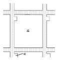
도 2a는 본 발명의 일 실시예에 따른 감지 소자의 제1 패터닝 공정 후의 평면도이다.
도 2b는 본 발명의 일 실시예에 따른 감지 소자의 제1 패터닝 공정 후의 단면도이다.
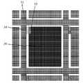
도 3a는 본 발명의 일 실시예에 따른 감지 소자의 제2 패터닝 공정 후의 평면도이다.
도 3b는 본 발명의 일 실시예에 따른 감지 소자의 제2 패터닝 공정 후의 단면도이다.
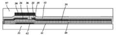
도 4a는 본 발명의 일 실시예에 따른 감지 소자의 제3 패터닝 공정 후의 평면도이다.
도 4b는 본 발명의 일 실시예에 따른 감지 소자의 제3 패터닝 공정 후의 단면도이다.
도 5a는 본 발명의 일 실시예에 따른 감지 소자의 제4 패터닝 공정 후의 평면도이다.
도 5b는 본 발명의 일 실시예에 따른 감지 소자의 제4 패터닝 공정 후의 단면도이다.In order to clearly illustrate the technical solution of embodiments of the present invention, the drawings of the embodiments will be briefly described below. It is to be understood that the drawings described relate only to some embodiments of the invention and not to limit the invention.
Figure 1 schematically illustrates a three-dimensional (3D) configuration of a conventional sensor.
2A is a plan view of a sensing element after a first patterning process according to an embodiment of the present invention.
FIG. 2B is a cross-sectional view of the sensing element after the first patterning process according to an embodiment of the present invention. FIG.
3A is a plan view of a sensing element after a second patterning process according to an embodiment of the present invention.
FIG. 3B is a cross-sectional view of a sensing element after a second patterning process according to an embodiment of the present invention. FIG.
4A is a plan view of a sensing device after a third patterning process according to an embodiment of the present invention.
4B is a cross-sectional view of the sensing element after the third patterning process according to an embodiment of the present invention.
5A is a plan view of a sensing element after a fourth patterning process according to an embodiment of the present invention.
FIG. 5B is a cross-sectional view of a sensing device according to an embodiment of the present invention after a fourth patterning process. FIG.
본 발명의 실시예들의 목적들, 기술 상세들 및 이점들을 분명하게 하기 위하여, 실시예의 기술적 해법들은 본 발명의 실시예들에 관련된 도면들에 연계하여 분명하고 충분히 이해할 수 있는 방식으로 설명될 것이다. 설명된 실시예들은 본 발명의 실시예들의 전부가 아니라 일부일 뿐이라는 것은 자명하다. 본 명세서의 설명된 실시예들에 기초하여, 당업자들은 어떤 창의적인 노력 없이도 본 발명의 범위 안에 해당하는 다른 실시예(들)를 얻을 수 있다.In order to clarify the objects, technical details and advantages of the embodiments of the present invention, the technical solutions of the embodiments will be described in a clear and fully understandable manner in connection with the drawings related to the embodiments of the present invention. It is to be understood that the described embodiments are not all, but only some of the embodiments of the invention. Based on the embodiments described herein, one of ordinary skill in the art can derive other embodiments (s) that fall within the scope of the invention without any creative effort.
본 명세서에서 사용된 모든 기술 및 과학 용어들은, 다르게 정의되지 않는 한, 본 발명이 속하는 기술 분야의 통상의 기술자가 일반적으로 이해하는 것과 동일한 의미를 가진다. "접속하다", "접속된" 등의 구절들은 물리적 연결이나 기계적 연결만을 정의하려고 하는 것이 아니라, 직접 또는 간접적인 전기적 접속까지 포함할 수 있다. "위", "아래", "오른쪽", "왼쪽" 등은 단지 상대적 위치 관계를 나타내기 위해 사용되며, 기술된 물체의 위치가 바뀔 경우, 그에 따라 상대적 위치 관계도 바뀔 수 있다.All technical and scientific terms used herein have the same meaning as commonly understood by one of ordinary skill in the art to which this invention belongs, unless otherwise defined. The phrases "connect", "connected", etc., may not only define physical or mechanical connections, but may also include direct or indirect electrical connections. "Up", "Down", "Right", "Left" and the like are used only to indicate relative positional relationships, and when the position of the described object is changed, the relative positional relationship can be changed accordingly.
아래 기술된 본 발명의 실시예들에서, 센서는 X선 센서 등, 여러 유형의 센서를 포함할 수 있다. 본 발명의 일 실시예에 따른 센서는 복수의 게이트 라인, 복수의 데이터 라인 및 상기 게이트 라인들과 상기 데이터 라인들에 의해 구획되고 어레이로서 배열된 복수의 감지 소자를 포함하고; 각각의 감지 소자는 TFT 디바이스와 포토다이오드 감지 디바이스를 포함한다. 다음의 설명들 및 도면들은 단일 감지 소자에 관련되어 있지만, 다른 감지 소자들도 같은 방법으로 형성될 수 있다.In the embodiments of the invention described below, the sensor may comprise various types of sensors, such as an X-ray sensor. A sensor according to an embodiment of the present invention includes a plurality of gate lines, a plurality of data lines, and a plurality of sensing elements partitioned by the gate lines and the data lines and arranged as an array; Each sensing element includes a TFT device and a photodiode sensing device. While the following description and drawings relate to a single sensing element, other sensing elements may be formed in the same manner.
본 발명의 일 실시예는 종래 기술에서의 높은 제조 비용과 복잡한 제조 공정들과 생산 능력 향상에서의 어려움을 갖는 센서들의 기술적 문제점을 해결하기 위한 센서 제조 방법을 제공한다. 이 방법은 다음 단계들을 포함한다:An embodiment of the present invention provides a method of manufacturing a sensor for solving the technical problems of sensors having high manufacturing cost and complicated manufacturing processes and difficulty in improving the production capacity in the prior art. The method includes the following steps:
단계 101: 단일 패터닝 공정이 베이스 기판(32) 상에 바이어스 라인(42)의 패턴을 형성하는 데 이용된다.Step 101: A single patterning process is used to form a pattern of
제1 패터닝 공정 후의 기판의 구성에 대해서는 도 2a 및 2b를 참조한다. 편의상, 도 2b는 기판 상의 감지 소자들 중 하나의 단면만을 보여준다. 도 3b, 4b 및 5b는 유사한 방식으로 도시되어 있다.The structure of the substrate after the first patterning process is described with reference to FIGS. 2A and 2B. For convenience, Figure 2b shows only one cross section of one of the sensing elements on the substrate. Figures 3b, 4b and 5b are shown in a similar manner.
일반적으로, 패터닝 공정은 순차적으로 기판 클리닝, 막 형성, 포토레지스트 도포, 노광, 현상, 식각, 포토레지스트 제거 등의 단계들을 포함한다. 기판은 탈이온수 또는 유기 세제를 사용하여 클리닝될 수 있다. 막 형성 공정은 패터닝될 구조 층들을 형성하는 데 사용된다. 예를 들어, 금속층은 일반적으로 물리 기상 증착(PVD)(예를 들어 마그네트론 스퍼터링)을 이용하여 형성되고, 이어서 습식 식각하여 패턴을 형성한다. 반면 비금속층은 보통 화학 기상 증착(CVD)을 이용하여 형성되고, 이어서 건식 식각하여 패턴을 형성한다. 다음 단계들에서의 패터닝 공정들은 동일하므로 상세히 설명하지 않는다.Generally, the patterning process sequentially includes steps such as substrate cleaning, film formation, photoresist application, exposure, development, etching, photoresist removal, and the like. The substrate may be cleaned using deionized water or an organic detergent. The film-forming process is used to form the structure layers to be patterned. For example, metal layers are typically formed using physical vapor deposition (PVD) (e.g., magnetron sputtering), followed by wet etching to form a pattern. On the other hand, the nonmetal layer is usually formed using chemical vapor deposition (CVD), followed by dry etching to form a pattern. The patterning processes in the following steps are the same and therefore will not be described in detail.
본 발명의 일 실시예에서, 베이스 기판(32)은 유리 기판, 플라스틱 기판 또는 다른 재료로 만들어진 기판일 수 있다. 바이어스 라인(42)의 재료는 알루미늄 네오디뮴(AlNd) 합금, 알루미늄(Al), 구리(Cu), 몰리브덴(Mo), 몰리브덴 텅스텐(MoW) 합금 또는 크롬(Cr)으로 만들어진 단층의 막, 또는 이들 금속 원소들 또는 합금 재료들의 임의의 조합으로 만들어진 다층 막일 수 있다. 단층 또는 다층 막은 예를 들어 150㎚ 내지 450㎚의 두께를 가질 수 있다.In one embodiment of the present invention, the
단계 102: 단일 패터닝 공정이 바이어스 라인(42) 상에 이와 전기적으로 접촉하는 투명 전극(41)의 패턴, 투명 전극(41) 상에 포토다이오드(40)의 패턴, 포토다이오드(40) 상에 수신 전극(39)의 패턴, 수신 전극(39)에 접속된 소스 전극(33)의 패턴 및 채널을 형성하기 위해 소스 전극(33)에 대향하여 배치된 드레인 전극(34)의 패턴, 및 드레인 전극(34)에 접속된 데이터 라인(31)의 패턴 및 소스 전극(33)과 드레인 전극(34) 상에 오믹층의 패턴을 형성하는 데 이용된다. 제2 패터닝 공정 후의 기판의 구성에 대해서는 도 3a 및 3b를 참조하자.Step 102: A single patterning process is carried out to form a pattern of
본 발명의 일 실시예에서, 투명 전극(41)의 재료는 인듐 주석 산화물(ITO) 또는 인듐 아연 산화물(IZO) 등의 투명한 도전 재료일 수 있다. 소스 전극(33), 드레인 전극(34), 데이터 라인(31) 및 수신 전극(39)은 동일한 재료로 이루어지거나 상이한 재료로 이루어질 수 있다. 바람직하게는, 이들은 동일한 재료(예를 들어 바이어스 라인과 동일한 재료)로 만들어지고 따라서 이들은 동일한 하나의 증착 및 식각을 통해 형성될 수 있어 제조 공정을 단순화하고 생산 능률을 향상시킬 수 있다. 오믹층(35)의 재료는 예를 들어 도핑된 반도체(n+a-Si)일 수 있다.In one embodiment of the present invention, the material of the
본 발명의 일 실시예에서, 포토다이오드(40)는 PIN 포토다이오드일 수 있는데, PIN 포토다이오드는 작은 접합 커패시턴스(junction capacitance), 짧은 주행 시간(transit time) 및 높은 감도를 가지는 이점들이 있기 때문이다. 그러나, 본 발명의 다른 실시예들에서, 포토다이오드는 MIS(Metal-Insulator-Semiconductor)-타입 포토다이오드 등일 수 있다.In one embodiment of the present invention, the
더 구체적으로, 본 발명의 일 실시예에서, 상기 단계 102는 다음의 단계들을 포함할 수 있다:More specifically, in one embodiment of the present invention, step 102 may include the following steps:
102a: 투명 도전 재료층, 포토다이오드 재료층, 데이터 라인 금속층 및 오믹 재료층을 순차적으로 증착하고, 오믹 재료층 상에 포토레지스트를 도포하는 단계;102a: sequentially depositing a transparent conductive material layer, a photodiode material layer, a data line metal layer and an ohmic material layer, and applying a photoresist on the ohmic material layer;
102b: 광-투과 부분, 부분-광-투과 부분 및 광-차단 부분을 가진 마스크를 이용하여 기판 상의 포토레지스트를 노광 및 현상하여 포토레지스트-완전-제거된 영역, 포토레지스트-부분-제거된 영역 및 포토레지스트-완전-유지된 영역을 가진 포토레지스트 패턴을 얻는 단계;102b: exposing and developing the photoresist on the substrate using a mask having a light-transmitting portion, a light-transmitting portion and a light-shielding portion to form a photoresist-completely-removed region, a photoresist- And obtaining a photoresist pattern having a photoresist-fully-retained region;
102c: 기판 상의 포토레지스트-완전-제거된 영역을 식각하는 단계; 및102c: etching the photoresist-completely-removed region on the substrate; And
102d: 포토레지스트-부분-제거된 영역 내의 포토레지스트를 제거하고 포토레지스트-완전-유지된 영역 내의 포토레지스트를 유지하도록 기판 상의 포토레지스트-부분-제거된 영역을 애싱(ashing)하고, 그리고 나서 식각한 후에 포토레지스트를 제거하여 채널의 패턴을 형성하는 단계.102d: ashing the photoresist-partially-removed region on the substrate to remove the photoresist in the photoresist-partially-removed region and retain the photoresist in the photoresist-fully-retained region, And removing the photoresist to form a pattern of channels.
상기 설명에서는, 포지티브형 포토레지스트가 포토레지스트의 예로서 사용되는데, 마스크의 광-투과 부분, 부분-광-투과 부분 및 광-차단 부분은 각각 포토레지스트를 전체 노광하고, 부분 노광하고, 전혀 노광하지 않도록 사용되며, 포토레지스트-완전-제거된 영역, 포토레지스트-부분-제거된 영역 및 포토레지스트-완전-유지된 영역을 얻도록 포토레지스트가 현상된다. 포토레지스트-완전-유지된 영역 내의 포토레지스트는 실질적으로 완전히 유지된다.In the above description, a positive type photoresist is used as an example of a photoresist, in which the light-transmitting portion, the light-transmitting portion and the light-blocking portion of the mask are subjected to full exposure, partial exposure, And the photoresist is developed to obtain a photoresist-completely-removed region, a photoresist-partially-removed region, and a photoresist-fully-retained region. The photoresist in the photoresist-fully-retained region is substantially completely retained.
포토다이오드(40)가 PIN 다이오드인 경우, 상기 단계 102a의 투명 도전 재료층 상에 포토다이오드 재료를 증착하는 것은 다음의 층들을 순차적으로 증착하는 것을 포함할 수 있다: P-타입 반도체층(p+a-Si), I-타입 반도체층(a-Si) 및 N-타입 반도체층(n+a-Si). 더 구체적으로, P-타입 반도체층은 투명 도전 재료층 상에 피착되고, I-타입 반도체층은 P-타입 반도체층 상에 피착되고, N-타입 반도체층은 I-타입 반도체층 상에 피착된다.If the
상기 단계 102b에서, 마스크의 부분-광-투과 부분은 그에 상응하여 채널을 가진 영역을 형성하고, 마스크의 광-차단 부분은 그에 상응하여 소스 전극(33), 드레인 전극(34), 데이터 라인(31) 및 수신 전극(39)을 가진 영역을 형성한다. 이 단계에서, 마스크는 듀얼-톤(dual-tone) 마스크(예를 들어, 그레이-톤(gray-tone) 마스크 또는 하프-톤(half-tone) 마스크)일 수 있다.The light-shielding portion of the mask corresponds to the
단계 103: 단일 패터닝 프로세스가 오믹층(35)과 채널의 위에 배치된 활성층(36)의 패턴, 활성층(36) 상에 있고 베이스 기판을 덮는 제1 패시베이션층(43)의 패턴, 제1 패시베이션층(43) 상에 및 채널의 위에 있는 게이트 전극(38)의 패턴, 및 게이트 전극(38)에 접속된 게이트 라인(30)의 패턴을 형성하는 데 이용된다. 제2 패터닝 공정 후의 기판의 구성에 대해서는 도 4a 및 4b를 참조하자.Step 103: A single patterning process is performed to form a pattern of the
본 발명의 일 실시예에서, 활성층(36)의 재료는 30㎚ 내지 250㎚의 두께를 가진 비정질 실리콘(a-Si) 등의 반도체 재료일 수 있고; 제1 패시베이션층(43)(및 하기에 기재된 제2 패시베이션층(57))의 재료는, 예를 들어, 1000㎚ 내지 2000㎚의 두께를 가진 무기 절연막(실리콘 질화물 등) 또는 유기 절연막(감광성 수지 재료 또는 비감광성 수지 등)일 수 있고; 게이트 전극(38) 및 게이트 라인(30)은 바이어스 라인(42)과 동일한 재료로 이루어질 수 있다.In one embodiment of the present invention, the material of the
더 구체적으로, 본 발명의 일 실시예에서, 상기 단계 103은 다음의 단계들을 포함할 수 있다:More specifically, in one embodiment of the present invention, step 103 may comprise the following steps:
103a: 활성 재료층, 제1 패시베이션층 및 게이트 금속층을 순차적으로 피착하는 단계;103a: sequentially depositing an active material layer, a first passivation layer and a gate metal layer;
103b: 게이트 금속층을 식각하여 게이트 전극(38)의 패턴 및 게이트 라인(30)의 패턴을 형성하는 단계.103b: etching the gate metal layer to form a pattern of the
상기 단계 103a에서, 활성층(36)의 패턴은 식각할 필요 없이 피착함으로써 바로 형성된다. 이는 베이스 기판(32)을 노출시키는 절단 영역(broken region)이 단계 102 후에 형성되기 때문이다. 활성 재료층은 (30㎚ 내지 250㎚의 두께로) 비교적 얇기 때문에, 절단 영역에서 절단되는 부분이 발생하므로, 따라서 활성층(36)의 패턴이 형성된다. 그러나, 제1 패시베이션층(43)은 비교적 두껍고, 따라서 거기에는 절단되는 부분이 형성되지 않는다.In this step 103a, the pattern of the
단계 104: 단일 패터닝 공정이 베이스 기판을 덮는 제2 패시베이션층(57)의 패턴을 형성하는 데 이용되고, 제2 패시베이션층(57)은 신호-전송 영역 비아 홀(signal-transmitting area via hole)을 가진다. 도 5a 및 5b에 도시된 것과 같은 기판의 구성이 상기 4개의 패터닝 공정을 이용해 형성된다. 도 5b는 본 발명의 실시예에 따른 센서의 감지 소자의 단면이므로, 기판의 주변부에 신호-전송 영역 비아 홀은 도시되어 있지 않다.Step 104: A single patterning process is used to form the pattern of the
본 발명은 단계 104 없이도 실현될 수 있으므로, 단계 104는 선택적이라는 데 유의하자. 그러므로, 일 실시예에서, 센서 제조 방법은 상기 단계 101 내지 단계 103만을 포함할 수 있다.Note that since the present invention can be realized without step 104, step 104 is optional. Therefore, in one embodiment, the sensor manufacturing method may include only steps 101 to 103 described above.
상기로부터 본 발명의 센서 제조 방법은 합해서 3개 또는 4개의 패터닝 공정을 이용하여도 됨이 확인된다. 종래 기술과 비교하여, 이는 사용되는 마스크의 수뿐만 아니라 생산 비용을 감소시키고 생산 공정을 단순화하여, 생산 능력과 수율을 크게 향상시킨다.From the above, it can be confirmed that the sensor manufacturing method of the present invention may use three or four patterning processes in total. Compared with the prior art, this greatly reduces the production cost as well as the number of masks used, simplifies the production process, and greatly improves production capacity and yield.
본 발명의 상기 실시예에 따른 제조 방법을 이용하여 도 5a 및 5b에 도시된 것과 같은 구성들을 가진 센서가 얻어진다. 이 센서는 베이스 기판(32), 서로 교차하여 배열된 게이트 라인(30)의 그룹 및 데이터 라인(31)의 그룹, 및 이 게이트 라인(30)의 그룹 및 데이터 라인(31)의 그룹에 의해 정의되고 어레이로 배열된 복수의 감지 소자를 포함한다. 각각의 감지 소자는 TFT 디바이스와 포토다이오드 감지 디바이스를 포함한다.A sensor having the configurations as shown in Figs. 5A and 5B is obtained by using the manufacturing method according to the embodiment of the present invention. This sensor is defined by a
포토다이오드 감지 디바이스는 베이스 기판(32) 상에 배치된 바이어스 라인(42); 이 바이어스 라인(42) 상에 배치되고 이와 전기적으로 접촉하는 투명 전극(41); 이 투명 전극(41) 상에 배치된 포토다이오드(40); 및 이 포토다이오드(40) 상에 배치된 수신 전극(39)을 포함한다.The photodiode sensing device includes a bias line (42) disposed on a base substrate (32); A
TFT 디바이스는 포토다이오드(40) 상에 배치되고 수신 전극(39)에 접속된 소스 전극(33); 포토다이오드(40) 상에 배치되고 이웃 데이터 라인(31)에 접속된 드레인 전극(34) - 소스 전극(33)과 드레인 전극(34)은 채널을 형성하기 위해 서로 대향하여 배치됨 -; 소스 전극(33)과 드레인 전극(34) 상에 배치된 오믹층(35); 오믹층(35)과 채널의 위에 배치된 활성층(36); 이 활성층(36) 상에 배치되고 베이스 기판을 덮는 제1 패시베이션층(43); 및 이 제1 패시베이션층(43) 상에서 채널 위쪽에 배치된 게이트 전극(38) - 이 게이트 전극은 이웃 게이트 라인(30)에 접속됨 - 을 포함한다.The TFT device includes a
일 실시예에서, 센서는 게이트 전극(38) 상에 배치되고 베이스 기판을 덮는 제2 패시베이션층(57)을 더 포함할 수 있고, 제2 패시베이션층(57)은 신호-전송 비아 홀을 가진다.In one embodiment, the sensor may further include a
이 실시예에서, 바이어스 라인(42)은 격자그물 형상을 가지고, 격자그물 내의 각 격자가 감지 소자에 대응한다(도 3a에 도시된 바와 같이). 한편, 바이어스 라인의 형상은 격자그물에 제한되는 것은 아니다. 예를 들어, 그것은 데이터 라인 또는 게이트 라인에 평행하게 배치될 수도 있다.In this embodiment, the
이 센서에서, 바이어스 라인은 베이스 기판 상에 제1 층으로 제조된다. 센서가 기능할 때, 광은 베이스 기판의 한 면으로부터 입사되고 베이스 기판을 통해 포토다이오드 감지 디바이스로 곧장 투과된다. 종래의 센서들과 비교하여, 광 손실이 크게 감소되고 광 흡수율이 향상되며, 화질이 개선되고 전력 소비가 감소된다.In this sensor, a bias line is fabricated as a first layer on a base substrate. When the sensor is functioning, light is incident from one side of the base substrate and is transmitted directly through the base substrate to the photodiode sensing device. Compared with conventional sensors, the optical loss is greatly reduced, the light absorption rate is improved, the image quality is improved, and the power consumption is reduced.
위에 설명한 것은 본 개시 내용의 예시적인 실시예들에 관한 것으로 본 개시 내용의 범위를 제한하는 것이 아니며, 본 개시 내용의 범위는 첨부한 청구항들에 의해 규정된다.It is not intended to be exhaustive or to limit the scope of the disclosure to the exemplary embodiments of the disclosure, and the scope of the disclosure is defined by the appended claims.
12: 센서; 13: 포토다이오드; 14: FET
15: 스캔 라인 16: 데이터 라인 17: 접속 핀
18: 데이터 판독 회로 30: 게이트 라인 31: 데이터 라인
32: 베이스 기판 33: 소스 전극 34: 드레인 전극
35: 오믹층 36: 활성층 42: 바이어스 라인
38: 게이트 전극 39: 수신 전극 40: 포토다이오드
41: 투명 전극 57: 제2 패시베이션층
43: 제1 패시베이션층12: sensor; 13: photodiode; 14: FET
15: scan line 16: data line 17: connection pin
18: data reading circuit 30: gate line 31: data line
32: base substrate 33: source electrode 34: drain electrode
35: ohmic layer 36: active layer 42: bias line
38: gate electrode 39: receiving electrode 40: photodiode
41: transparent electrode 57: second passivation layer
43: first passivation layer
Claims (8)
Translated fromKorean제1 패터닝 공정을 이용하여 베이스 기판 상에 바이어스 라인의 패턴을 형성하는 단계;
제2 패터닝 공정을 이용하여, 상기 바이어스 라인 상에 이와 전기적으로 접촉하는 투명 전극의 패턴, 상기 투명 전극 상에 포토다이오드의 패턴, 상기 포토다이오드 상에 수신 전극의 패턴, 상기 수신 전극에 접속된 소스 전극의 패턴과 채널을 형성하도록 상기 소스 전극에 대향하여 배치된 드레인 전극의 패턴, 상기 드레인 전극에 접속된 데이터 라인의 패턴, 및 상기 소스 전극 및 상기 드레인 전극 상에 오믹(ohmic) 층의 패턴을 형성하는 단계;
제3 패터닝 공정을 이용하여, 상기 오믹층과 상기 채널 상에 활성층의 패턴, 상기 활성층 상에 있고 상기 베이스 기판을 덮는 제1 패시베이션층의 패턴, 상기 제1 패시베이션층 상에서 상기 채널 위에 있는 게이트 전극의 패턴, 및 상기 게이트 전극에 접속된 게이트 라인의 패턴을 형성하는 단계
를 포함하는, 센서 제조 방법.A method of manufacturing a sensor,
Forming a pattern of bias lines on the base substrate using a first patterning process;
A pattern of the transparent electrode on the bias line, a pattern of the photodiode on the transparent electrode, a pattern of the receiving electrode on the photodiode, a pattern of the source connected to the receiving electrode, A pattern of a drain electrode disposed opposite to the source electrode to form a pattern of an electrode and a channel, a pattern of a data line connected to the drain electrode, and a pattern of an ohmic layer on the source electrode and the drain electrode ;
A third patterning process is used to form a pattern of the active layer on the ohmic layer and the channel, a pattern of a first passivation layer on the active layer and covering the base substrate, a pattern of a gate electrode on the channel on the first passivation layer Forming a pattern of a gate line connected to the gate electrode,
Gt;
제4 패터닝 공정을 이용하여 상기 베이스 기판을 덮는 제2 패시베이션층의 패턴을 형성하는 단계를 더 포함하고, 상기 제2 패시베이션층은 신호-전송 영역 비아 홀(signal-transmitting area via hole)을 가지는, 센서 제조 방법.2. The method of claim 1, further comprising: after forming the pattern of the gate electrode and the pattern of the gate line:
Forming a pattern of a second passivation layer over the base substrate using a fourth patterning process, the second passivation layer having a signal-transmitting area via hole, Sensor manufacturing method.
투명 도전 재료층, 포토다이오드 재료층, 데이터 라인 금속층 및 오믹 재료층을 순차적으로 피착하고, 상기 오믹 재료층 상에 포토레지스트를 도포하는 단계;
광-투과 부분, 부분-광-투과 부분 및 광-차단 부분을 가진 마스크를 이용하여 상기 베이스 기판 상의 상기 포토레지스트를 노광 및 현상하여 포토레지스트-완전-제거된 영역, 포토레지스트-부분-제거된 영역 및 포토레지스트-완전-유지된 영역을 가진 포토레지스트 패턴을 얻는 단계;
상기 베이스 기판 상의 상기 포토레지스트-완전-제거된 영역을 식각하는 단계; 및
상기 포토레지스트-부분-제거된 영역 내의 상기 포토레지스트를 제거하고 상기 포토레지스트-완전-유지된 영역 내의 상기 포토레지스트의 두께를 줄여 부분적으로 유지하도록 상기 베이스 기판 상의 포토레지스트-부분-제거된 영역을 애싱(ashing)하고, 그리고 나서 식각한 후에 상기 포토레지스트를 제거하여 상기 채널의 패턴을 형성하는 단계
를 포함하는, 센서 제조 방법.3. The method according to claim 1 or 2, wherein the pattern of the transparent electrode, the pattern of the photodiode, the pattern of the receiving electrode, the pattern of the source electrode, the pattern of the drain electrode, Forming a pattern of lines and a pattern of the ohmic layer comprises:
Sequentially depositing a transparent conductive material layer, a photodiode material layer, a data line metal layer, and an ohmic material layer, and applying a photoresist on the ohmic material layer;
The photoresist on the base substrate is exposed and developed using a mask having a light-transmissive portion, a partially-light-transmissive portion and a light-intercepting portion to form a photoresist-completely-removed region, a photoresist- Obtaining a photoresist pattern having regions and photoresist-fully-retained regions;
Etching the photoresist-completely-removed region on the base substrate; And
Removing the photoresist in the photoresist-partially-removed region and partially removing the photoresist-partially-removed region on the base substrate to reduce the thickness of the photoresist in the photoresist-fully- Ashing, and then removing the photoresist after etching to form a pattern of the channel
Gt;
활성 재료층, 제1 패시베이션층 및 게이트 금속층을 순차적으로 피착하고, 상기 활성층의 패턴이 형성되는 단계;
상기 게이트 금속층을 식각하여 상기 게이트 전극의 패턴 및 상기 게이트 라인의 패턴을 형성하는 단계
를 포함하는, 센서 제조 방법.The method of claim 1, wherein forming the pattern of the active layer, the pattern of the first passivation layer, the pattern of the gate electrode, and the pattern of the gate line using the third patterning process comprises:
Sequentially depositing an active material layer, a first passivation layer and a gate metal layer, and forming a pattern of the active layer;
Etching the gate metal layer to form a pattern of the gate electrode and a pattern of the gate line
Gt;
5. The method of claim 4, wherein depositing the photodiode material layer comprises sequentially depositing a P-type semiconductor layer, an I-type semiconductor layer, and an N-type semiconductor layer.
Applications Claiming Priority (3)
| Application Number | Priority Date | Filing Date | Title |
|---|---|---|---|
| CN201210262971.4 | 2012-07-26 | ||
| CN201210262971.4ACN102790068B (en) | 2012-07-26 | 2012-07-26 | Manufacturing method for sensor |
| PCT/CN2012/084775WO2014015583A1 (en) | 2012-07-26 | 2012-11-16 | Method for manufacturing sensor |
Publications (2)
| Publication Number | Publication Date |
|---|---|
| KR20140068812A KR20140068812A (en) | 2014-06-09 |
| KR101530143B1true KR101530143B1 (en) | 2015-06-18 |
Family
ID=47155429
Family Applications (1)
| Application Number | Title | Priority Date | Filing Date |
|---|---|---|---|
| KR1020137035100AActiveKR101530143B1 (en) | 2012-07-26 | 2012-11-16 | Method for fabricating sensor |
Country Status (6)
| Country | Link |
|---|---|
| US (1) | US9171879B2 (en) |
| EP (1) | EP2879180B1 (en) |
| JP (1) | JP6053929B2 (en) |
| KR (1) | KR101530143B1 (en) |
| CN (1) | CN102790068B (en) |
| WO (1) | WO2014015583A1 (en) |
Families Citing this family (2)
| Publication number | Priority date | Publication date | Assignee | Title |
|---|---|---|---|---|
| JP7272472B2 (en)* | 2017-05-24 | 2023-05-12 | コニカミノルタ株式会社 | Radiographic imaging device and radiographic imaging system |
| EP3874926B1 (en)* | 2018-10-30 | 2022-12-21 | Tokyo Keiki Inc. | Error correction apparatus |
Citations (3)
| Publication number | Priority date | Publication date | Assignee | Title |
|---|---|---|---|---|
| US5306648A (en)* | 1986-01-24 | 1994-04-26 | Canon Kabushiki Kaisha | Method of making photoelectric conversion device |
| US20110263084A1 (en)* | 2010-04-23 | 2011-10-27 | Semiconductor Energy Laboratory Co., Ltd. | Method for manufacturing semiconductor device |
| KR20120027541A (en)* | 2009-06-17 | 2012-03-21 | 더 리젠츠 오브 더 유니버시티 오브 미시간 | Photodiode and other sensor structures in flat-panel x-ray imagers and method for improving topological uniformity of the photodiode and other sensor structures in flat-panel x-ray imagers based on thin-film electronics |
Family Cites Families (13)
| Publication number | Priority date | Publication date | Assignee | Title |
|---|---|---|---|---|
| DE3751242T2 (en)* | 1986-01-24 | 1995-09-14 | Canon Kk | Photoelectric converter. |
| JPS6450465A (en)* | 1987-08-20 | 1989-02-27 | Canon Kk | Semiconductor device |
| JP3482073B2 (en)* | 1996-07-01 | 2003-12-22 | 松下電器産業株式会社 | Method for manufacturing thin film transistor array |
| JP3267218B2 (en)* | 1997-11-27 | 2002-03-18 | 松下電器産業株式会社 | Liquid crystal display with image reading function |
| JP2003258226A (en)* | 2002-02-27 | 2003-09-12 | Canon Inc | Radiation detection device and method of manufacturing the same |
| KR100763913B1 (en)* | 2006-04-27 | 2007-10-05 | 삼성전자주식회사 | Manufacturing Method of Thin Film Transistor |
| TWI333275B (en)* | 2008-05-09 | 2010-11-11 | Au Optronics Corp | Method for fabricating light sensor |
| JP2011159782A (en)* | 2010-02-01 | 2011-08-18 | Epson Imaging Devices Corp | Photoelectric conversion device, x-ray imaging device, and method of manufacturing photoelectric conversion device |
| CN102790061B (en)* | 2012-07-26 | 2016-05-11 | 北京京东方光电科技有限公司 | A kind of sensor and manufacture method thereof |
| CN102790069B (en)* | 2012-07-26 | 2014-09-10 | 北京京东方光电科技有限公司 | Sensor and manufacturing method thereof |
| CN102790063B (en)* | 2012-07-26 | 2017-10-17 | 北京京东方光电科技有限公司 | A kind of sensor and its manufacture method |
| CN102790062B (en)* | 2012-07-26 | 2016-01-27 | 北京京东方光电科技有限公司 | A kind of manufacture method of transducer |
| CN102790067B (en)* | 2012-07-26 | 2014-12-10 | 北京京东方光电科技有限公司 | Sensor and manufacturing method thereof |
- 2012
- 2012-07-26CNCN201210262971.4Apatent/CN102790068B/enactiveActive
- 2012-11-16KRKR1020137035100Apatent/KR101530143B1/enactiveActive
- 2012-11-16JPJP2015523366Apatent/JP6053929B2/enactiveActive
- 2012-11-16WOPCT/CN2012/084775patent/WO2014015583A1/enactiveApplication Filing
- 2012-11-16USUS14/123,992patent/US9171879B2/enactiveActive
- 2012-11-16EPEP12881532.1Apatent/EP2879180B1/enactiveActive
Patent Citations (3)
| Publication number | Priority date | Publication date | Assignee | Title |
|---|---|---|---|---|
| US5306648A (en)* | 1986-01-24 | 1994-04-26 | Canon Kabushiki Kaisha | Method of making photoelectric conversion device |
| KR20120027541A (en)* | 2009-06-17 | 2012-03-21 | 더 리젠츠 오브 더 유니버시티 오브 미시간 | Photodiode and other sensor structures in flat-panel x-ray imagers and method for improving topological uniformity of the photodiode and other sensor structures in flat-panel x-ray imagers based on thin-film electronics |
| US20110263084A1 (en)* | 2010-04-23 | 2011-10-27 | Semiconductor Energy Laboratory Co., Ltd. | Method for manufacturing semiconductor device |
Also Published As
| Publication number | Publication date |
|---|---|
| KR20140068812A (en) | 2014-06-09 |
| EP2879180B1 (en) | 2017-07-05 |
| US20150194461A1 (en) | 2015-07-09 |
| EP2879180A1 (en) | 2015-06-03 |
| CN102790068B (en) | 2014-10-22 |
| JP6053929B2 (en) | 2016-12-27 |
| JP2015530733A (en) | 2015-10-15 |
| WO2014015583A1 (en) | 2014-01-30 |
| EP2879180A4 (en) | 2016-03-30 |
| US9171879B2 (en) | 2015-10-27 |
| CN102790068A (en) | 2012-11-21 |
Similar Documents
| Publication | Publication Date | Title |
|---|---|---|
| US9236518B2 (en) | Sensor and method for fabricating the same | |
| EP2879178B1 (en) | Sensor and manufacturing method therefor | |
| US9318629B2 (en) | Method for fabricating sensor using multiple patterning processes | |
| US9312290B2 (en) | Sensor and method for fabricating the same | |
| US8962371B2 (en) | Method for fabricating sensor | |
| WO2014015604A1 (en) | Sensor and method for manufacturing same | |
| US9024320B2 (en) | Sensor and method for manufacturing the same | |
| KR101530143B1 (en) | Method for fabricating sensor | |
| KR101543946B1 (en) | Method for fabricating sensor | |
| WO2014015603A1 (en) | Sensor and method for manufacturing same | |
| US9490279B2 (en) | Sensor including TFT device and photodiode sensing device and method for fabricating the same |
Legal Events
| Date | Code | Title | Description |
|---|---|---|---|
| A201 | Request for examination | ||
| PA0105 | International application | Patent event date:20131231 Patent event code:PA01051R01D Comment text:International Patent Application | |
| PA0201 | Request for examination | Patent event code:PA02012R01D Patent event date:20131231 Comment text:Request for Examination of Application | |
| N231 | Notification of change of applicant | ||
| PN2301 | Change of applicant | Patent event date:20140326 Comment text:Notification of Change of Applicant Patent event code:PN23011R01D | |
| PG1501 | Laying open of application | ||
| E902 | Notification of reason for refusal | ||
| PE0902 | Notice of grounds for rejection | Comment text:Notification of reason for refusal Patent event date:20150129 Patent event code:PE09021S01D | |
| E701 | Decision to grant or registration of patent right | ||
| PE0701 | Decision of registration | Patent event code:PE07011S01D Comment text:Decision to Grant Registration Patent event date:20150602 | |
| GRNT | Written decision to grant | ||
| PR0701 | Registration of establishment | Comment text:Registration of Establishment Patent event date:20150612 Patent event code:PR07011E01D | |
| PR1002 | Payment of registration fee | Payment date:20150612 End annual number:3 Start annual number:1 | |
| PG1601 | Publication of registration | ||
| FPAY | Annual fee payment | Payment date:20180530 Year of fee payment:4 | |
| PR1001 | Payment of annual fee | Payment date:20180530 Start annual number:4 End annual number:4 | |
| FPAY | Annual fee payment | Payment date:20190530 Year of fee payment:5 | |
| PR1001 | Payment of annual fee | Payment date:20190530 Start annual number:5 End annual number:5 | |
| PR1001 | Payment of annual fee | Payment date:20200603 Start annual number:6 End annual number:6 | |
| PR1001 | Payment of annual fee | Payment date:20210517 Start annual number:7 End annual number:7 | |
| PR1001 | Payment of annual fee | Payment date:20240430 Start annual number:10 End annual number:10 | |
| PR1001 | Payment of annual fee | Payment date:20250428 Start annual number:11 End annual number:11 |