KR101529675B1 - Multi-chip package memory device - Google Patents
Multi-chip package memory deviceDownload PDFInfo
- Publication number
- KR101529675B1 KR101529675B1KR1020080134980AKR20080134980AKR101529675B1KR 101529675 B1KR101529675 B1KR 101529675B1KR 1020080134980 AKR1020080134980 AKR 1020080134980AKR 20080134980 AKR20080134980 AKR 20080134980AKR 101529675 B1KR101529675 B1KR 101529675B1
- Authority
- KR
- South Korea
- Prior art keywords
- memory
- command
- chip
- control signal
- memory chip
- Prior art date
- Legal status (The legal status is an assumption and is not a legal conclusion. Google has not performed a legal analysis and makes no representation as to the accuracy of the status listed.)
- Active
Links
Images


Classifications
- H—ELECTRICITY
- H01—ELECTRIC ELEMENTS
- H01L—SEMICONDUCTOR DEVICES NOT COVERED BY CLASS H10
- H01L23/00—Details of semiconductor or other solid state devices
- H01L23/12—Mountings, e.g. non-detachable insulating substrates
- H—ELECTRICITY
- H01—ELECTRIC ELEMENTS
- H01L—SEMICONDUCTOR DEVICES NOT COVERED BY CLASS H10
- H01L25/00—Assemblies consisting of a plurality of semiconductor or other solid state devices
- H01L25/18—Assemblies consisting of a plurality of semiconductor or other solid state devices the devices being of the types provided for in two or more different main groups of the same subclass of H10B, H10D, H10F, H10H, H10K or H10N
- G—PHYSICS
- G11—INFORMATION STORAGE
- G11C—STATIC STORES
- G11C5/00—Details of stores covered by group G11C11/00
- G11C5/02—Disposition of storage elements, e.g. in the form of a matrix array
- G11C5/04—Supports for storage elements, e.g. memory modules; Mounting or fixing of storage elements on such supports
- H—ELECTRICITY
- H01—ELECTRIC ELEMENTS
- H01L—SEMICONDUCTOR DEVICES NOT COVERED BY CLASS H10
- H01L25/00—Assemblies consisting of a plurality of semiconductor or other solid state devices
- H01L25/03—Assemblies consisting of a plurality of semiconductor or other solid state devices all the devices being of a type provided for in a single subclass of subclasses H10B, H10D, H10F, H10H, H10K or H10N, e.g. assemblies of rectifier diodes
- H01L25/04—Assemblies consisting of a plurality of semiconductor or other solid state devices all the devices being of a type provided for in a single subclass of subclasses H10B, H10D, H10F, H10H, H10K or H10N, e.g. assemblies of rectifier diodes the devices not having separate containers
- H01L25/065—Assemblies consisting of a plurality of semiconductor or other solid state devices all the devices being of a type provided for in a single subclass of subclasses H10B, H10D, H10F, H10H, H10K or H10N, e.g. assemblies of rectifier diodes the devices not having separate containers the devices being of a type provided for in group H10D89/00
- H01L25/0657—Stacked arrangements of devices
- H—ELECTRICITY
- H01—ELECTRIC ELEMENTS
- H01L—SEMICONDUCTOR DEVICES NOT COVERED BY CLASS H10
- H01L2224/00—Indexing scheme for arrangements for connecting or disconnecting semiconductor or solid-state bodies and methods related thereto as covered by H01L24/00
- H01L2224/01—Means for bonding being attached to, or being formed on, the surface to be connected, e.g. chip-to-package, die-attach, "first-level" interconnects; Manufacturing methods related thereto
- H01L2224/02—Bonding areas; Manufacturing methods related thereto
- H01L2224/04—Structure, shape, material or disposition of the bonding areas prior to the connecting process
- H01L2224/0401—Bonding areas specifically adapted for bump connectors, e.g. under bump metallisation [UBM]
- H—ELECTRICITY
- H01—ELECTRIC ELEMENTS
- H01L—SEMICONDUCTOR DEVICES NOT COVERED BY CLASS H10
- H01L2224/00—Indexing scheme for arrangements for connecting or disconnecting semiconductor or solid-state bodies and methods related thereto as covered by H01L24/00
- H01L2224/01—Means for bonding being attached to, or being formed on, the surface to be connected, e.g. chip-to-package, die-attach, "first-level" interconnects; Manufacturing methods related thereto
- H01L2224/02—Bonding areas; Manufacturing methods related thereto
- H01L2224/04—Structure, shape, material or disposition of the bonding areas prior to the connecting process
- H01L2224/05—Structure, shape, material or disposition of the bonding areas prior to the connecting process of an individual bonding area
- H01L2224/0554—External layer
- H01L2224/0556—Disposition
- H01L2224/0557—Disposition the external layer being disposed on a via connection of the semiconductor or solid-state body
- H—ELECTRICITY
- H01—ELECTRIC ELEMENTS
- H01L—SEMICONDUCTOR DEVICES NOT COVERED BY CLASS H10
- H01L2224/00—Indexing scheme for arrangements for connecting or disconnecting semiconductor or solid-state bodies and methods related thereto as covered by H01L24/00
- H01L2224/01—Means for bonding being attached to, or being formed on, the surface to be connected, e.g. chip-to-package, die-attach, "first-level" interconnects; Manufacturing methods related thereto
- H01L2224/10—Bump connectors; Manufacturing methods related thereto
- H01L2224/15—Structure, shape, material or disposition of the bump connectors after the connecting process
- H01L2224/16—Structure, shape, material or disposition of the bump connectors after the connecting process of an individual bump connector
- H01L2224/161—Disposition
- H01L2224/16135—Disposition the bump connector connecting between different semiconductor or solid-state bodies, i.e. chip-to-chip
- H01L2224/16145—Disposition the bump connector connecting between different semiconductor or solid-state bodies, i.e. chip-to-chip the bodies being stacked
- H—ELECTRICITY
- H01—ELECTRIC ELEMENTS
- H01L—SEMICONDUCTOR DEVICES NOT COVERED BY CLASS H10
- H01L2225/00—Details relating to assemblies covered by the group H01L25/00 but not provided for in its subgroups
- H01L2225/03—All the devices being of a type provided for in the same main group of the same subclass of class H10, e.g. assemblies of rectifier diodes
- H01L2225/04—All the devices being of a type provided for in the same main group of the same subclass of class H10, e.g. assemblies of rectifier diodes the devices not having separate containers
- H01L2225/065—All the devices being of a type provided for in the same main group of the same subclass of class H10
- H01L2225/06503—Stacked arrangements of devices
- H01L2225/06513—Bump or bump-like direct electrical connections between devices, e.g. flip-chip connection, solder bumps
- H—ELECTRICITY
- H01—ELECTRIC ELEMENTS
- H01L—SEMICONDUCTOR DEVICES NOT COVERED BY CLASS H10
- H01L2225/00—Details relating to assemblies covered by the group H01L25/00 but not provided for in its subgroups
- H01L2225/03—All the devices being of a type provided for in the same main group of the same subclass of class H10, e.g. assemblies of rectifier diodes
- H01L2225/04—All the devices being of a type provided for in the same main group of the same subclass of class H10, e.g. assemblies of rectifier diodes the devices not having separate containers
- H01L2225/065—All the devices being of a type provided for in the same main group of the same subclass of class H10
- H01L2225/06503—Stacked arrangements of devices
- H01L2225/06517—Bump or bump-like direct electrical connections from device to substrate
- H—ELECTRICITY
- H01—ELECTRIC ELEMENTS
- H01L—SEMICONDUCTOR DEVICES NOT COVERED BY CLASS H10
- H01L2225/00—Details relating to assemblies covered by the group H01L25/00 but not provided for in its subgroups
- H01L2225/03—All the devices being of a type provided for in the same main group of the same subclass of class H10, e.g. assemblies of rectifier diodes
- H01L2225/04—All the devices being of a type provided for in the same main group of the same subclass of class H10, e.g. assemblies of rectifier diodes the devices not having separate containers
- H01L2225/065—All the devices being of a type provided for in the same main group of the same subclass of class H10
- H01L2225/06503—Stacked arrangements of devices
- H01L2225/06541—Conductive via connections through the device, e.g. vertical interconnects, through silicon via [TSV]
- H—ELECTRICITY
- H01—ELECTRIC ELEMENTS
- H01L—SEMICONDUCTOR DEVICES NOT COVERED BY CLASS H10
- H01L2225/00—Details relating to assemblies covered by the group H01L25/00 but not provided for in its subgroups
- H01L2225/03—All the devices being of a type provided for in the same main group of the same subclass of class H10, e.g. assemblies of rectifier diodes
- H01L2225/04—All the devices being of a type provided for in the same main group of the same subclass of class H10, e.g. assemblies of rectifier diodes the devices not having separate containers
- H01L2225/065—All the devices being of a type provided for in the same main group of the same subclass of class H10
- H01L2225/06503—Stacked arrangements of devices
- H01L2225/06555—Geometry of the stack, e.g. form of the devices, geometry to facilitate stacking
- H01L2225/06565—Geometry of the stack, e.g. form of the devices, geometry to facilitate stacking the devices having the same size and there being no auxiliary carrier between the devices
- H—ELECTRICITY
- H01—ELECTRIC ELEMENTS
- H01L—SEMICONDUCTOR DEVICES NOT COVERED BY CLASS H10
- H01L2924/00—Indexing scheme for arrangements or methods for connecting or disconnecting semiconductor or solid-state bodies as covered by H01L24/00
- H01L2924/0001—Technical content checked by a classifier
- H01L2924/0002—Not covered by any one of groups H01L24/00, H01L24/00 and H01L2224/00
- H—ELECTRICITY
- H01—ELECTRIC ELEMENTS
- H01L—SEMICONDUCTOR DEVICES NOT COVERED BY CLASS H10
- H01L2924/00—Indexing scheme for arrangements or methods for connecting or disconnecting semiconductor or solid-state bodies as covered by H01L24/00
- H01L2924/01—Chemical elements
- H01L2924/01019—Potassium [K]
- H—ELECTRICITY
- H01—ELECTRIC ELEMENTS
- H01L—SEMICONDUCTOR DEVICES NOT COVERED BY CLASS H10
- H01L2924/00—Indexing scheme for arrangements or methods for connecting or disconnecting semiconductor or solid-state bodies as covered by H01L24/00
- H01L2924/15—Details of package parts other than the semiconductor or other solid state devices to be connected
- H01L2924/151—Die mounting substrate
- H01L2924/153—Connection portion
- H01L2924/1531—Connection portion the connection portion being formed only on the surface of the substrate opposite to the die mounting surface
- H01L2924/15311—Connection portion the connection portion being formed only on the surface of the substrate opposite to the die mounting surface being a ball array, e.g. BGA
Landscapes
- Engineering & Computer Science (AREA)
- Microelectronics & Electronic Packaging (AREA)
- Power Engineering (AREA)
- Physics & Mathematics (AREA)
- Condensed Matter Physics & Semiconductors (AREA)
- General Physics & Mathematics (AREA)
- Computer Hardware Design (AREA)
- Dram (AREA)
Abstract
Translated fromKorean
Description
Translated fromKorean본 발명은 메모리 장치에 관한 것으로, 특히 메모리 칩들이 적층된 멀티 칩 패키지 메모리 장치에 관한 것이다.The present invention relates to a memory device, and more particularly to a multi-chip package memory device in which memory chips are stacked.
최근 전자 휴대기기의 크기가 소형화됨에 따라 전자 휴대기기 내부에 장착되는 반도체 패키지도 점차 소형화 및 경량화되고 있는 반면, 반도체패키지에 내장되는 메모리 칩의 용량은 증대되고 있다. 따라서, 기존에는 하나의 기능을 수행하는 메모리 칩이 내장된 싱글 칩 패키지 메모리(single-chip package memory)를 사용하였으나, 최근에는 두 가지 이상의 다른 기능을 수행하는 복수 개의 메모리 칩이 적층된(stacked) 멀티 칩 패키지 메모리(multi-chip package memory)가 제조되고 있다.2. Description of the Related Art [0002] With the recent miniaturization of electronic portable devices, semiconductor packages to be mounted in electronic portable devices are becoming smaller and lighter, while the capacity of memory chips incorporated in semiconductor packages is increasing. Therefore, in the past, a single-chip package memory having a built-in memory chip has been used. However, recently, a plurality of memory chips performing two or more different functions are stacked, A multi-chip package memory is being manufactured.
상기 멀티 칩 패키지 메모리에서 메모리 칩을 적층하는 방법으로는 인터페이스 칩(interface chip)과 다수개의 메모리 칩을 적층하는 방법 및 메모리 컨트롤러와 다수개의 메모리 칩을 적층하는 방법 등이 있다.Methods for stacking memory chips in the multi-chip package memory include a method of stacking an interface chip and a plurality of memory chips, a method of stacking a memory controller and a plurality of memory chips, and the like.
예를 들어, 제 1 및 제 2 메모리 칩을 적층하는 경우, 종래의 멀티 칩 패키지 메모리는 각각의 메모리 칩과 패드를 본딩 와이어에 의하여 전기적으로 연결하 였다. 즉, 제 1 메모리 칩과 제 1 패드를 본딩 와이어에 의하여 전기적으로 연결하고, 제 2 메모리 칩과 제 2 패드를 본딩 와이어에 의하여 전기적으로 연결하였다.For example, when the first and second memory chips are stacked, the conventional multi-chip package memory electrically connects each memory chip and a pad by a bonding wire. That is, the first memory chip and the first pad are electrically connected by a bonding wire, and the second memory chip and the second pad are electrically connected by a bonding wire.
본 발명이 해결하고자 하는 과제는 프로세스 변화량(process variation)이 상이한 복수의 메모리 칩을 적층한 경우 안정적으로 동작할 수 있는 멀티 칩 패키지 메모리 장치(multi-chip package memory device)를 제공하는데 있다.SUMMARY OF THE INVENTION It is an object of the present invention to provide a multi-chip package memory device capable of operating stably when a plurality of memory chips having different process variations are stacked.
상기 과제를 달성하기 위한 본 발명의 일 실시예에 따른 멀티 칩 패키지 메모리 장치는 전달 메모리 칩 및 상기 전달 메모리 칩 위에 적층되는 복수의 메모리 칩들을 구비할 수 있다. 상기 전달 메모리 칩은 임시 저장부를 구비하고, 수신된 커맨드 또는 데이터를 대응하는 메모리 칩 또는 외부로 전달할 수 있다. 상기 각각의 메모리 칩은 메모리 코어를 구비하고, 상기 메모리 칩의 특성에 따라 수신된 커맨드를 지연시킨 지연 커맨드를 각각 출력할 수 있다. 상기 전달 메모리 칩은 상기 각각의 지연 커맨드가 수신되는 경우마다 상기 임시 저장부의 다른 위치에 상기 수신된 데이터를 저장할 수 있다.According to an aspect of the present invention, there is provided a multi-chip package memory device including a transfer memory chip and a plurality of memory chips stacked on the transfer memory chip. The transfer memory chip has a temporary storage unit and can transfer the received command or data to the corresponding memory chip or to the outside. Each of the memory chips has a memory core, and can output a delay command delaying the received command according to the characteristics of the memory chip. The transfer memory chip may store the received data at different locations in the temporary storage whenever the respective delay commands are received.
상기 전달 메모리 칩은 상기 지연 커맨드가 수신되는 경우마다 비트가 순차적으로 이동된 제어 신호를 발생하는 제어 신호 발생부를 더 구비하고, 상기 임시 저장부는 상기 제어 신호에 응답하여 상기 수신된 데이터를 저장하는 것이 바람직하다.Wherein the transfer memory chip further comprises a control signal generator for generating a control signal in which bits are sequentially shifted each time the delay command is received, wherein the temporary storage unit stores the received data in response to the control signal desirable.
상기 각각의 메모리 칩은 게이트에 대응하는 지연 커맨드가 인가되고 제 1 단은 제 1 노드에 연결되며 제 2 단은 접지 전압에 연결되는 트랜지스터를 구비하 고, 상기 전달 메모리 칩은 상기 제 1 노드 및 전원 전압 사이에 연결되는 저항을 구비하며, 상기 제어 신호 발생부는 상기 제 1 노드와 상기 임시 저장부 사이에 연결되고 상기 제 1 노드를 통하여 인가되는 신호에 응답하여 상기 제어 신호를 발생하는 것이 바람직하다.Wherein each memory chip has a transistor with a delay command corresponding to a gate, the first end connected to a first node and the second end connected to a ground voltage, Wherein the control signal generator is connected between the first node and the temporary storage unit and generates the control signal in response to a signal applied through the first node, .
상기 전달 메모리 칩은 상기 수신된 지연 커맨드를 논리합 연산하여 순차적으로 출력하는 연산부를 더 구비하고, 상기 제어 신호 발생부는 상기 연산부의 출력 신호에 응답하여 상기 제어 신호를 발생하는 것이 바람직하다.The transfer memory chip may further include an operation unit for performing an OR operation on the received delay command and sequentially outputting the delay command, and the control signal generation unit may generate the control signal in response to an output signal of the operation unit.
상기 연산부는 게이트에 각각의 지연 커맨드가 인가되고 제 1 단은 제 1 노드에 연결되며 제 2 단은 접지 전압에 연결되는 복수의 트랜지스터들 및 상기 제 1 노드 및 전원 전압 사이에 연결되는 저항을 구비하는 것이 바람직하다.The arithmetic section has a plurality of transistors each having a gate to which a delay command is applied, a first end connected to a first node, a second end connected to a ground voltage, and a resistor connected between the first node and the power supply voltage .
상기 각각의 메모리 칩은 상기 수신된 커맨드가 상기 메모리 코어를 액세스하는데 걸리는 시간만큼 상기 수신된 커맨드를 지연시켜 상기 지연 커맨드로서 출력하는 지연부를 구비하는 것이 바람직하다.And each of the memory chips includes a delay unit that delays the received command by a time required for the received command to access the memory core and outputs the delayed command as the delay command.
상기 전달 메모리 칩은 메모리 코어를 더 구비하고, 상기 대응하는 메모리 칩의 특성에 따라 상기 수신된 커맨드를 지연시킨 지연 커맨드를 출력하는 것이 바람직하다.Preferably, the transfer memory chip further includes a memory core, and outputs a delay command that delays the received command according to characteristics of the corresponding memory chip.
본 발명에 따른 멀티 칩 패키지 메모리 장치(multi-chip package memory device)는 프로세스 변화량(process variation)이 상이한 복수의 메모리 칩을 적층한 경우에도 수신된 커맨드를 안정적으로 수행할 수 있는 장점이 있다.The multi-chip package memory device according to the present invention has an advantage that the received commands can be stably executed even when a plurality of memory chips having different process variations are stacked.
본 발명과 본 발명의 동작상의 이점 및 본 발명의 실시에 의하여 달성되는 목적을 충분히 이해하기 위해서는 본 발명의 바람직한 실시예를 예시하는 첨부 도면 및 도면에 기재된 내용을 참조하여야 한다.In order to fully understand the present invention, operational advantages of the present invention, and objects achieved by the practice of the present invention, reference should be made to the accompanying drawings and the accompanying drawings which illustrate preferred embodiments of the present invention.
이하, 첨부한 도면을 참조하여 본 발명의 바람직한 실시예를 설명함으로써, 본 발명을 상세히 설명한다. 각 도면에 제시된 동일한 참조부호는 동일한 부재를 나타낸다.BEST MODE FOR CARRYING OUT THE INVENTION Hereinafter, the present invention will be described in detail with reference to the preferred embodiments of the present invention with reference to the accompanying drawings. Like reference symbols in the drawings denote like elements.
도 1은 전달 메모리 칩 위에 수직 방향으로 적층된 메모리 칩들을 구비하는 멀티 칩 패키지 메모리 장치(multi-chip package memory device)를 나타내는 도면이다.1 is a diagram illustrating a multi-chip package memory device having memory chips stacked vertically on a transfer memory chip.
도 1을 참조하면, 4개의 메모리 칩들(CHIP1, ... , CHIP4)이 전달 메모리 칩(CHIP_INT) 상에 수직 방향으로 적층된다. 물론, 적층되는 메모리 칩의 개수는 4개에 한정되지 않는다.Referring to Fig. 1, four memory chips (CHIP1, ..., CHIP4) are vertically stacked on a transfer memory chip (CHIP_INT). Of course, the number of stacked memory chips is not limited to four.
전달 메모리 칩(CHIP_INT)은 외부에서 수신되는 신호들(예를 들어, 커맨드)을 메모리 칩들(CHIP1, ... , CHIP4)에 전달하거나 메모리 칩들(CHIP1, ... , CHIP4)의 데이터를 외부로 전달한다. 메모리 칩들(CHIP1, ... , CHIP4)과 전달 메모리 칩(CHIP_INT)은 관통 전극들(TSV1~TSV5)을 통하여 서로 연결되거나 또는 패키지(PKG)에 연결된다. 수직 방향으로 적층된 메모리 칩들(CHIP1, ... , CHIP4)과 전달 메모리 칩(CHIP_INT)은 관통 전극들(TSV1, ... , TSV5)을 통하여 데이터 또는 신호등을 송수신한다.The transfer memory chip CHIP_INT transfers external signals (e.g., a command) to the memory chips CHIP1, ..., CHIP4 or data of the memory chips CHIP1, ..., CHIP4, . The memory chips CHIP1 to CHIP4 and the transfer memory chip CHIP_INT are connected to each other through the penetrating electrodes TSV1 to TSV5 or connected to the package PKG. The memory chips CHIP1 through CHIP4 and the transfer memory chip CHIP_INT stacked in the vertical direction transmit and receive data or signals through the penetrating electrodes TSV1 through TSV5.
도 2는 도 1의 멀티 칩 패키지 메모리 장치의 개략적인 블록도이다.2 is a schematic block diagram of the multi-chip package memory device of FIG.
도 2를 참조하면, 도 1의 멀티 칩 패키지 메모리 장치는 복수개의 메모리 칩들(CHIP1, ... , CHIP4) 및 전달 메모리 칩(CHIP_INT)을 구비한다. 각각의 메모리 칩(예를 들어, CHIP1)은 메모리 코어(220_1), 로우 디코더(230_1), 칼럼 디코더(240_1) 및 입출력 드라이버(250_1)을 구비한다. 전달 메모리 칩(CHIP_INT)은 기입 버퍼(270), 기입 제어부(275), 독출 버퍼(280) 및 독출 제어부(285)를 구비한다.Referring to FIG. 2, the multi-chip package memory device of FIG. 1 includes a plurality of memory chips (CHIP1, ..., CHIP4) and a transfer memory chip (CHIP_INT). Each memory chip (for example, CHIP1) includes a memory core 220_1, a row decoder 230_1, a column decoder 240_1, and an input / output driver 250_1. The transfer memory chip CHIP_INT includes a
기입 데이터(WDATA)는 기입 제어부(275), 기입 버퍼(270) 및 입출력 드라이버(250_1)를 거쳐서 메모리 코어(220_1)에 기입된다. 독출 데이터(RDATA)는 메모리 코어(220_1), 입출력 드라이버(250_1), 독출 버퍼(280) 및 독출 제어부(285)를 거쳐서 외부로 독출된다. 로우 디코더(230_1)와 칼럼 디코더(240_1)는 메모리 코어(220_1)의 어드레스들 중에서 기입 또는 독출 대상 어드레스를 지정한다.The write data WDATA is written to the memory core 220_1 via the
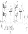
도 3은 본 발명의 일 실시예에 따른 멀티 칩 패키지 메모리 장치(300)의 블록도이다.3 is a block diagram of a multi-chip
도 3을 참조하면, 멀티 칩 패키지 메모리 장치(300)는 전달 메모리 칩(310) 및 전달 메모리 칩(310) 위에 적층되는 복수의 메모리 칩들(340_1, 340_2, ... )을 구비할 수 있다. 도 3에서는 제 1 메모리 칩(340_1) 및 제 2 메모리 칩(340_2)에 대하여만 도시하였으나, 동일한 구성의 메모리 칩이 복수 개 적층될 수 있다. 도 3에서는 n 개(n은 자연수)의 메모리 칩이 적층되는 경우를 가정하여 n 개의 독출된 데이터(RDARA_1, RDARA_2, ... , RDATA_n)가 전송되는 경우를 도시하였다.3, the multi-chip
전달 메모리 칩(310)은 임시 저장부(320) 및 제어 신호 발생부(330)를 구비할 수 있다. 전달 메모리 칩(310)은 수신된 커맨드 또는 데이터를 대응하는 메모리 칩 또는 외부로 전달하는 인터페이스 칩일 수 있다. 예를 들어, 전달 메모리 칩(310)은 독출 커맨드(CMD)가 수신된 경우 독출 커맨드(CMD)를 상기 메모리 칩들 중 대응하는 메모리 칩으로 전송할 수 있고, 상기 메모리 칩들에서 독출된 데이터(RDATA_1, RDATA_2, ... , RDATA_n)를 수신하여 외부로 전달할 수 있다. 임시 저장부(320)는 FIFO(first-in first-out) 유닛일 수 있고, 제어 신호 발생부(330)는 쉬프트 레지스터일 수 있다.The
각각의 메모리 칩(340_1, 340_2)은 동일한 구성을 가지므로 이하에서는 편의상 제 1 메모리 칩(340_1)에 대하여 설명한다.Since each of the memory chips 340_1 and 340_2 has the same configuration, the first memory chip 340_1 will be described for the sake of convenience.
제 1 메모리 칩(340_1)은 메모리 코어(350_1), 커맨드 디코더(360_1) 및 지연 제어부(370_1)를 구비할 수 있다. 메모리 코어(350_1)는 데이터가 저장되는 복수의 메모리 셀을 포함할 수 있다. 커맨드 디코더(360_1)는 수신한 커맨드(CMD)를 디코딩하여 디코딩 커맨드(CMD_DEC)를 출력한다. 이하에서는 본 발명의 구성요소들이 디코딩 커맨드(CMD_DEC)에 기초하여 동작하는 것으로 설명하고 있으나, 본 발명의 구성요소들은 커맨드(CMD)에 기초하여 동작할 수도 있다. 지연 제어부(370_1)는 디코딩 커맨드(CMD_DEC)가 메모리 코어(350_1)를 액세스하는데 걸리는 시간만큼 디코딩 커맨드(CMD_DEC)를 지연시켜 지연 커맨드(CMD_D1)로서 출력할 수 있다.The first memory chip 340_1 may include a memory core 350_1, a command decoder 360_1, and a delay controller 370_1. The memory core 350_1 may include a plurality of memory cells in which data is stored. The command decoder 360_1 decodes the received command CMD and outputs a decoding command CMD_DEC. Hereinafter, although the components of the present invention are described as operating based on the decoding command CMD_DEC, the elements of the present invention may operate based on the command CMD. The delay control section 370_1 can output the delay command CMD_D1 by delaying the decoding command CMD_DEC by the time required for the decoding command CMD_DEC to access the memory core 350_1.
만약, 상기 적층되는 메모리 칩의 프로세스 변화량(process variation)이 상이한 경우, 각각의 지연 제어부(370_1, 370_2)는 대응하는 메모리 칩의 프로세스 변화량에 따라 디코딩 커맨드(CMD_DEC)를 다른 정도로 지연하여 출력한다. 상기 프로세스 변화량이란 소정의 커맨드가 수신되고 상기 커맨드가 수행될 때까지의 시간을 의미한다. 예를 들어, 각각의 메모리 코어가 독출 커맨드를 수신하고 데이터를 독출할 때까지 걸리는 시간을 상기 프로세스 변화량이라고 할 수 있다. 제 1 메모리 칩(340_1)의 프로세스 변화량이 9 [ns]이고, 제 2 메모리 칩(340_2)의 프로세스 변화량이 11 [ns]라고 가정하자. 이 경우 지연 제어부(370_1)는 수신된 디코딩 커맨드(CMD_DEC)를 9 [ns]만큼 지연하여 출력하고, 지연 제어부(370_2)는 수신된 디코딩 커맨드(CMD_DEC)를 11 [ns]만큼 지연하여 출력할 수 있다.If the process variations of the stacked memory chips are different, each of the delay controllers 370_1 and 370_2 delays the decoding command CMD_DEC according to the amount of process variation of the corresponding memory chip, and outputs the delayed command CMD_DEC to another extent. The process change amount means a time until a predetermined command is received and the command is executed. For example, the time taken for each memory core to receive a read command and read data is referred to as the process variation amount. Assume that the process variation amount of the first memory chip 340_1 is 9 [ns] and the process variation amount of the second memory chip 340_2 is 11 [ns]. In this case, the delay control unit 370_1 delays the received decoding command CMD_DEC by 9 [ns], and the delay control unit 370_2 delays the received decoding command CMD_DEC by 11 [ns] have.
또한, 제 1 메모리 칩(340_1)은 대응하는 지연 커맨드(CMD_D1)가 게이트에 인가되고 제 1 단은 제 1 노드(n1)에 연결되며 제 2 단은 접지 전압(VSS)에 연결되는 트랜지스터(TR1)를 구비할 수 있다. 또한, 전달 메모리 칩(310)은 제 1 노드(n1)와 전원 전압(VDD) 사이에 연결되는 저항(R)을 구비할 수 있다. 상기 각각의 트랜지스터를 이용함으로서 전달 메모리 칩(310)은 각각의 메모리 칩에서 독출 커맨드가 전송되었는지를 알 수 있다.The first memory chip 340_1 is connected to the gate of the transistor TR1 whose first end is connected to the first node n1 and whose second end is connected to the ground voltage VSS, ). Also, the
도 3의 경우 트랜지스터들(TR1, TR2, ...)이 대응하는 메모리 칩(340_1, 340_2, ...)에 포함되는 경우에 대하여 도시하고 있으나, 트랜지스터들(TR1, TR2, ...) 및 저항(R)이 각각 대응하는 메모리 칩(340_1, 340_2, ...) 및 전달 메모리 칩(310)에 포함되지 않을 수도 있다. 이 경우, 지연 커맨드(CMD_D1, CMD_D2, ... )가 전달 메모리 칩(310)으로 직접 전송되거나, 전달 메모리 칩(310)은 수신된 지연 커맨드(CMD_D1, CMD_D2, ... )를 논리합 연산하여 순차적으로 출력 하는 연산부(미도시)를 더 구비할 수도 있다. 상기 연산부는 트랜지스터들(TR1, TR2, ...) 및 저항(R)을 구비할 수 있다. 즉, 각각 대응하는 메모리 칩(340_1, 340_2, ...)에 구현되어 있는 트랜지스터들(TR1, TR2, ...)을 전달 메모리 칩(310)에서 구현할 수 있다.In the case of FIG. 3, the transistors TR1, TR2, ... are included in the corresponding memory chips 340_1, 340_2, And the resistor R may not be included in the corresponding memory chips 340_1, 340_2, ..., and the
트랜지스터들(TR1, TR2, ...)이 대응하는 메모리 칩(340_1, 340_2, ...)에 포함되는 경우, 전달 메모리 칩(310)은 제 1 노드(n1)를 통하여 인가되는 신호에 응답하여 각각의 지연 커맨드(CMD_D1, CMD_D2, ... )가 수신되는 경우마다 임시 저장부(320)의 다른 위치에 대응하는 수신된 데이터(RDATA_1, RDATA_2, ... , RDATA_n)를 저장한다. 전달 메모리 칩(310)이 지연 커맨드(CMD_D1, CMD_D2, ... )를 직접 수신한 경우, 각각의 지연 커맨드(CMD_D1, CMD_D2, ... )가 수신되는 경우마다 임시 저장부(320)의 다른 위치에 대응하는 수신된 데이터(RDATA_1, RDATA_2, ... , RDATA_n)를 저장한다. 제어 신호 발생부(330)는 각각의 지연 커맨드(CMD_D1, CMD_D2, ... )가 수신되는 경우마다 비트가 순차적으로 이동된 제어 신호(CON)를 발생할 수 있다. 임시 저장부(320) 및 제어 신호 발생부(330)에 대하여는 도 5 및 도 6을 참조하여 보다 상세하게 설명한다.When the transistors TR1, TR2, ... are included in the corresponding memory chips 340_1, 340_2, ..., the
도 4는 본 발명의 다른 일 실시예에 따른 멀티 칩 패키지 메모리 장치(400)의 블록도이다.4 is a block diagram of a multi-chip
도 3 및 도 4를 참조하면, 멀티 칩 패키지 메모리 장치(400)는 도 3과 유사하게 전달 메모리 칩(410) 및 전달 메모리 칩(410) 위에 적층되는 복수의 메모리 칩들(340_1, 340_2, ... )를 구비할 수 있다. 다만, 도 3의 전달 메모리 칩(310)과 상이하게 도 4의 전달 메모리 칩(410)은 메모리 코어(350_0)를 포함하고 있다. 즉, 전달 메모리 칩(410)은 상기 메모리 칩의 기능 및 상기 인터페이스 칩의 기능을 모두 수행할 수 있다. 전달 메모리 칩(410)은 상기 메모리 칩의 기능을 수행하고 위하여 메모리 코어(350_0), 커맨드 디코더(360_0) 및 지연 제어부(370_0)를 포함할 수 있고, 상기 인터페이스 칩의 기능을 수행하기 위하여 제어 신호 발생부(430) 및 임시 저장부(420)를 포함할 수 있다. 또한, 앞서 설명한 트랜지스터와 동일한 기능을 하는 트랜지스터(TR0)를 더 포함할 수도 있다. 메모리 코어(350_0), 커맨드 디코더(360_0) 및 지연 제어부(370_0)는 앞서 설명한 도 3의 메모리 코어(350_1), 커맨드 디코더(360_1) 및 지연 제어부(370_1)와 동일한 기능을 수행하므로 이하에서 상세한 설명은 생략한다. 또한, 제어 신호 발생부(430) 및 임시 저장부(420) 각각은 도 3보다 하나 더 많은 데이터(RDATA_0) 및 지연 커맨드(CMD_D0)를 수신한다는 점을 제외하고는 동일하게 동작하므로 역시 상세한 설명은 생략한다. 즉, 도 4의 실시예는 도 3의 멀티 칩 패키지 메모리(300) 중 전달 메모리 칩(310)이 다른 메모리 칩과 같은 기능을 함께 수행할 수 있음도 보여주고 있다.3 and 4, a multi-chip
도 5(a) 내지 도 5(d)는 도 3 및 도 4의 제어 신호 발생부(330, 430)의 일 실시예에 따른 블록도이다.5 (a) to 5 (d) are block diagrams according to an embodiment of the
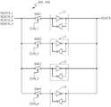
도 6은 도 3 및 도 4의 임시 저장부(320, 420)의 일 실시예에 따른 회로도이다.FIG. 6 is a circuit diagram according to an embodiment of the
도 3 내지 도 6을 참조하여 제어 신호 발생부(330, 430) 및 임시 저장부(320, 420)의 동작에 대하여 설명한다. 이하에서는 설명의 편의상 도 3의 멀티 칩 패키지 메모리 장치(300)가 독출 동작을 수행하는 경우에 대하여 설명한다. 또한, 상기 메모리 칩이 4개가 있다고 가정하고, 독출 커맨드(CMD)는 상기 제 1 내지 제 4 메모리 칩에 순차적으로 인가된다고 가정한다. 설명의 편의상 제 1 메모리 칩(340_1)에 인가되는 독출 커맨드를 제 1 독출 커맨드라고 하고, 제 2 메모리 칩(340_2)에 인가되는 독출 커맨드를 제 2 독출 커맨드라고 하고, 제 3 메모리 칩(미도시)에 인가되는 독출 커맨드를 제 3 독출 커맨드라고 하며, 제 4 메모리 칩(미도시)에 인가되는 독출 커맨드를 제 4 독출 커맨드라고 한다.The operations of the
먼저 상기 제 1 독출 커맨드가 제 1 메모리 칩(340_1)에 인가되면, 커맨드 디코더(360_1)는 상기 제 1 독출 커맨드를 디코딩하여 제 1 디코딩 커맨드로서 출력한다. 메모리 코어(350_1)는 상기 제 1 디코딩 커맨드에 응답하여 제 1 독출 데이터(RDATA_1)를 출력한다. 지연 제어부(370_1)는 메모리 코어(350_1)에서 독출 동작을 수행하데 걸리는 시간만큼 상기 제 1 디코딩 커맨드를 지연하여 제 1 지연 커맨드(CMD_D1)로서 출력한다.First, when the first read command is applied to the first memory chip 340_1, the command decoder 360_1 decodes the first read command and outputs the first read command as a first decoding command. The memory core 350_1 outputs the first read data RDATA_1 in response to the first decoding command. The delay control unit 370_1 delays the first decoding command by a time required for the memory core 350_1 to perform the read operation, and outputs the delayed command as the first delay command CMD_D1.
다음으로, 상기 제 2 독출 커맨드가 제 2 메모리 칩(340_2)에 인가되면, 커맨드 디코더(360_2)는 상기 제 2 독출 커맨드를 디코딩하여 제 2 디코딩 커맨드로서 출력한다. 메모리 코어(350_2)는 상기 제 2 디코딩 커맨드에 응답하여 제 2 독출 데이터(RDATA_2)를 출력한다. 지연 제어부(370_2)는 메모리 코어(350_2)에서 독출 동작을 수행하데 걸리는 시간만큼 상기 제 2 디코딩 커맨드를 지연하여 제 2 지연 커맨드(CMD_D2)로 출력한다.Next, when the second read command is applied to the second memory chip 340_2, the command decoder 360_2 decodes the second read command and outputs it as a second decode command. The memory core 350_2 outputs the second read data RDATA_2 in response to the second decoding command. The delay control unit 370_2 delays the second decoding command by a time required for the memory core 350_2 to perform the read operation, and outputs the second decoding command as the second delay command CMD_D2.
이후에, 제 3 및 제 4 독출 커맨드가 상기 제 3 및 제 4 메모리 칩에 순차적 으로 인가되면, 상기와 동일한 방법으로 제 3 및 제 4 독출 데이터와 제 3 및 제 4 지연 커맨드가 순차적으로 출력된다.Thereafter, when the third and fourth read commands are sequentially applied to the third and fourth memory chips, the third and fourth read data and the third and fourth delay commands are sequentially output in the same manner as described above .
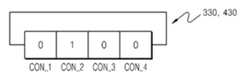
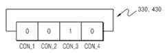
상기 제 1 내지 제 4 지연 커맨드가 순차적으로 출력되면, 대응하는 트랜지스터가 순차적으로 턴 온된다. 예를 들어, 지연 제어부(370_1)가 제 1 지연 커맨드(CMD_D1)를 출력하면 순간적으로 트랜지스터(TR1)가 턴 온되었다가 턴 오프된다. 따라서, 제어 신호 발생부(330)는 도 5(a)와 같은 값을 저장하게 되고, 제어 신호(CON)는 '1000'의 신호가 된다. 상기와 같은 값을 가지는 제어 신호(CON)에 응답하여, 임시 저장부(320)의 제 1 스위치(SWI1)는 온 상태가 되고, 제 2 내지 제 4 스위치(SWI2, SWI3, SWI4)는 오프 상태가 되어 제 1 래치(L1)에 제 1 독출 데이터(RDATA_1)가 저장된다.When the first to fourth delay commands are sequentially output, the corresponding transistors are sequentially turned on. For example, when the delay control unit 370_1 outputs the first delay command CMD_D1, the transistor TR1 is momentarily turned on and then turned off. Therefore, the
소정이 시간이 경과한 후, 지연 제어부(370_2)가 제 2 지연 커맨드(CMD_D2)를 출력하면 순간적으로 트랜지스터(TR2)가 턴 온되었다가 턴 오프된다. 따라서, 제어 신호 발생부(330)는 도 5(b)와 같은 값을 저장하게 되고, 제어 신호(CON)는 '0100'의 신호가 된다. 상기와 같은 값을 가지는 제어 신호(CON)에 응답하여, 임시 저장부(320)의 제 2 스위치(SWI2)는 온 상태가 되고, 제 1 스위치(SWI1), 제 3 스위치(SWI3) 및 제 4 스위치(SWI4)는 오프 상태가 되어 제 1 래치(L1)에 제 1 독출 데이터(RDATA_1)가 저장되는 동작을 종료하고 제 2 래치(L2)에 제 2 독출 데이터(RDATA_2)가 저장된다.After the predetermined time has elapsed, when the delay control unit 370_2 outputs the second delay command CMD_D2, the transistor TR2 is momentarily turned on and then turned off. Accordingly, the
동일한 방법에 의하여, 상기 제 3 지연 커맨드 및 상기 제 3 독출 데이터가 출력되는 경우 상기 제 3 독출 데이터는 제 3 래치(L3)에 저장되고, 상기 제 4 지 연 커맨드 및 상기 제 4 독출 데이터가 출력되는 경우 상기 제 4 독출 데이터는 제 4 래치(L4)에 저장된다.When the third delay command and the third read data are output by the same method, the third read data is stored in the third latch (L3), and the fourth delay command and the fourth read data are output The fourth read data is stored in the fourth latch L4.
이상에서는 설명의 편의상 도 3의 멀티 칩 패키지 메모리 장치(300)가 독출 동작을 수행하는 경우에 대하여 설명하였으나, 도 4의 멀티 칩 패키지 메모리 장치(400)가 동작하는 경우에도 임시 저장부(430) 및 제어 신호 발생부(430)는 동일한 방식으로 동작할 수 있다.Although the case where the multi-chip
도 7은 본 발명의 일 실시예에 따른 신호 및 데이터의 타이밍도이다.7 is a timing diagram of signals and data according to an embodiment of the present invention.
도 3 내지 도 7을 참조하여 본 발명의 일 실시예에 따른 동작을 설명한다. 이하에서도 설명의 편의상 도 3의 멀티 칩 패키지 메모리 장치(300)가 독출 동작을 하는 경우로 가정하여 설명한다. 다만, 도 4의 멀티 칩 패키지 메모리 장치(400)가 동작을 하는 경우도 동일하게 적용될 수 있다.The operation according to an embodiment of the present invention will be described with reference to FIGS. Hereinafter, it is assumed that the multichip
수신되는 커맨드(CMD)를 살펴보면, 순차적으로 제 1 독출 커맨드(RD1), 제 2 독출 커맨드(RD2), 제 3 독출 커맨드(RD3) 및 제 2 독출 커맨드(RD2)가 인가되고 있다. 이하에서, 제 k 독출 커맨드(k는 자연수)는 제 k 메모리 코어에 인가되는 신호라고 가정한다. 또한, 제 1 메모리 칩(340_1)의 독출 동작 시 프로세스 변화량은 9 [ns]이고, 제 2 메모리 칩(340_2)의 독출 동작 시 프로세스 변화량은 11 [ns]이며 상기 제 3 메모리 칩의 독출 동작 시 프로세스 변화량은 7.2 [ns]라고 가정한다.Referring to the received command CMD, the first read command RD1, the second read command RD2, the third read command RD3, and the second read command RD2 are sequentially applied. Hereinafter, it is assumed that the k-th read command (k is a natural number) is a signal applied to the k-th memory core. In addition, the process variation amount in the reading operation of the first memory chip 340_1 is 9 [ns], the process variation amount in the reading operation of the second memory chip 340_2 is 11 [ns] The process variation is assumed to be 7.2 [ns].
제 1 독출 커맨드(RD1)가 인가된 경우, 제 1 독출 데이터(RDATA_1)는 t1 시점부터 임시 저장부(320)에 인가된다. 다음으로, 제 2 독출 커맨드(RD2)가 인가된 경우 제 2 독출 데이터(RDATA_2)가 t2 시점부터 임시 저장부(320)에 인가되고, 제 3 독출 커맨드(RD3)가 인가된 경우 제 3 독출 데이터(RDATA_3)가 t3 시점부터 임시 저장부(320)에 인가되며, 마지막으로 제 2 독출 커맨드(RD2)가 다시 인가된 경우 t4 시점부터 제 2 독출 데이터(RDATA_2)가 t4 시점부터 임시 저장부(320)에 인가된다.When the first read command RD1 is applied, the first read data RDATA_1 is applied to the
각각의 지연 제어부는 대응하는 메모리 칩의 프로세스 변화량을 고려하여 상기 커맨드 신호를 지연하여 출력한다. 이하에서는 제 1 내지 제 3 독출 커맨드(RD1, RD2, RD3)가 디코딩 되지 않고 대응하는 지연 제어부에 인가된다고 가정한다. 즉, 제 1 메모리 칩(340_1)의 지연 제어부(370_1)는 제 1 독출 커맨드(RD1)를 9 [ns]만큼 지연하여 t1 시점에 제어 신호 발생부(330)에 인가한다. 제어 신호 발생부(330)는 t1 시점에 '1000'의 제어 신호(CON)를 출력하므로, 임시 저장부(320)는 제 1 독출 데이터(RDATA_1)를 제 1 래치(L1)에 저장한다. 이후에, 제 2 메모리 칩(340_2)의 제 2 지연 제어부(370_2)는 제 2 독출 커맨드(RD2)를 11 [ns]만큼 지연하여 t2 시점에 제어 신호 발생부(330)에 인가한다. 제어 신호 발생부(330)는 t2 시점에 '0100'의 제어 신호(CON)를 출력하므로, 임시 저장부(320)는 제 1 독출 데이터(RDATA_1)의 저장을 종료하고 제 2 독출 데이터(RDATA_2)를 제 2 래치(L2)에 저장한다. 다음으로, 상기 제 3 메모리 칩의 지연 제어부는 제 3 독출 커맨드(RD3)를 7.2 [ns]만큼 지연하여 t3 시점에 제어 신호 발생부(330)에 인가한다. 제어 신호 발생부(330)는 t3 시점에 '0010'의 제어 신호(CON)를 출력하므로, 임시 저장부(320)는 제 2 독출 데이터(RDATA_1)의 저장을 종료하고 제 3 독출 데이 터(RDATA_3)를 제 3 래치(L3)에 저장한다. 마지막으로, 제 2 메모리 칩(340_2)의 지연 제어부(370_2)는 제 2 독출 커맨드(RD2)를 11 [ns]만큼 지연하여 t4 시점에 제어 신호 발생부(330)에 인가한다. 제어 신호 발생부(330)는 t2 시점에 '0001'의 제어 신호(CON)를 출력하므로, 임시 저장부(320)는 제 3 독출 데이터(RDATA_3)의 저장을 종료하고 제 2 독출 데이터(RDATA_2)를 제 2 래치(L2)에 저장한다.Each delay control unit delays and outputs the command signal in consideration of the process variation amount of the corresponding memory chip. Hereinafter, it is assumed that the first to third read commands RD1, RD2, and RD3 are not decoded but are applied to the corresponding delay control units. That is, the delay control unit 370_1 of the first memory chip 340_1 delays the first read command RD1 by 9 [ns] and applies the delayed control signal to the control
따라서, 상기 각각의 독출된 데이터는 상기 각각의 메모리 칩의 프로세스 변화량이 다름에도 불구하고 중복되지 않으면서 임시 저장부(320, 420)에 저장될 수 있다.Therefore, each of the read data can be stored in the
이상에서와 같이 도면과 명세서에서 최적 실시예가 개시되었다. 여기서 특정한 용어들이 사용되었으나, 이는 단지 본 발명을 설명하기 위한 목적에서 사용된 것이지 의미한정이나 특허청구범위에 기재된 본 발명의 범위를 제한하기 위하여 사용된 것은 아니다. 그러므로 본 기술분야의 통상의 지식을 가진 자라면 이로부터 다양한 변형 및 균등한 타 실시예가 가능하다는 점을 이해할 것이다. 따라서, 본 발명의 진정한 기술적 보호범위는 첨부된 특허청구범위의 기술적 사상에 의해 정해져야 할 것이다.As described above, an optimal embodiment has been disclosed in the drawings and specification. Although specific terms have been employed herein, they are used for purposes of illustration only and are not intended to limit the scope of the invention as defined in the claims or the claims. Therefore, those skilled in the art will appreciate that various modifications and equivalent embodiments are possible without departing from the scope of the present invention. Accordingly, the true scope of the present invention should be determined by the technical idea of the appended claims.
본 발명의 상세한 설명에서 인용되는 도면을 보다 충분히 이해하기 위하여 각 도면의 간단한 설명이 제공된다.BRIEF DESCRIPTION OF THE DRAWINGS A brief description of each drawing is provided to more fully understand the drawings recited in the description of the invention.
도 1은 전달 메모리 칩 위에 수직 방향으로 적층된 메모리 칩들을 구비하는 멀티 칩 패키지 메모리 장치(multi-chip package memory device)를 나타내는 도면이다.1 is a diagram illustrating a multi-chip package memory device having memory chips stacked vertically on a transfer memory chip.
도 2는 도 1의 멀티 칩 패키지 메모리 장치의 개략적인 블록도이다.2 is a schematic block diagram of the multi-chip package memory device of FIG.
도 3은 본 발명의 일 실시예에 따른 멀티 칩 패키지 메모리 장치의 블록도이다.3 is a block diagram of a multi-chip package memory device in accordance with an embodiment of the present invention.
도 4는 본 발명의 다른 일 실시예에 따른 멀티 칩 패키지 메모리 장치의 블록도이다.4 is a block diagram of a multi-chip package memory device according to another embodiment of the present invention.
도 5(a) 내지 도 5(d)는 도 3 및 도 4의 제어 신호 발생부의 일 실시예에 따른 블록도이다.5 (a) to 5 (d) are block diagrams according to an embodiment of the control signal generator of FIG. 3 and FIG.
도 6은 도 3 및 도 4의 임시 저장부의 일 실시예에 따른 회로도이다.FIG. 6 is a circuit diagram according to one embodiment of the temporary storage unit of FIGS. 3 and 4. FIG.
도 7은 본 발명의 일 실시예에 따른 신호 및 데이터의 타이밍도이다.7 is a timing diagram of signals and data according to an embodiment of the present invention.
Claims (10)
Translated fromKoreanPriority Applications (2)
| Application Number | Priority Date | Filing Date | Title |
|---|---|---|---|
| KR1020080134980AKR101529675B1 (en) | 2008-12-26 | 2008-12-26 | Multi-chip package memory device |
| US12/619,083US8174115B2 (en) | 2008-12-26 | 2009-11-16 | Multi-chip package memory device |
Applications Claiming Priority (1)
| Application Number | Priority Date | Filing Date | Title |
|---|---|---|---|
| KR1020080134980AKR101529675B1 (en) | 2008-12-26 | 2008-12-26 | Multi-chip package memory device |
Publications (2)
| Publication Number | Publication Date |
|---|---|
| KR20100076809A KR20100076809A (en) | 2010-07-06 |
| KR101529675B1true KR101529675B1 (en) | 2015-06-29 |
Family
ID=42283887
Family Applications (1)
| Application Number | Title | Priority Date | Filing Date |
|---|---|---|---|
| KR1020080134980AActiveKR101529675B1 (en) | 2008-12-26 | 2008-12-26 | Multi-chip package memory device |
Country Status (2)
| Country | Link |
|---|---|
| US (1) | US8174115B2 (en) |
| KR (1) | KR101529675B1 (en) |
Families Citing this family (16)
| Publication number | Priority date | Publication date | Assignee | Title |
|---|---|---|---|---|
| US8787060B2 (en) | 2010-11-03 | 2014-07-22 | Netlist, Inc. | Method and apparatus for optimizing driver load in a memory package |
| JP2011082450A (en) | 2009-10-09 | 2011-04-21 | Elpida Memory Inc | Semiconductor device, and information processing system with the same |
| WO2012021310A1 (en)* | 2010-08-09 | 2012-02-16 | Rambus Inc. | Disaggregated semiconductor chip assembly and packaging technique |
| KR101190683B1 (en)* | 2010-10-29 | 2012-10-12 | 에스케이하이닉스 주식회사 | Semiconductor Apparatus, Method for Delaying Signal thereof, Stacked Semicionductor Memory Apparatus and Method for Generating Signal |
| US8930647B1 (en) | 2011-04-06 | 2015-01-06 | P4tents1, LLC | Multiple class memory systems |
| US9176671B1 (en) | 2011-04-06 | 2015-11-03 | P4tents1, LLC | Fetching data between thread execution in a flash/DRAM/embedded DRAM-equipped system |
| US9170744B1 (en) | 2011-04-06 | 2015-10-27 | P4tents1, LLC | Computer program product for controlling a flash/DRAM/embedded DRAM-equipped system |
| US9158546B1 (en) | 2011-04-06 | 2015-10-13 | P4tents1, LLC | Computer program product for fetching from a first physical memory between an execution of a plurality of threads associated with a second physical memory |
| US9432298B1 (en) | 2011-12-09 | 2016-08-30 | P4tents1, LLC | System, method, and computer program product for improving memory systems |
| US9164679B2 (en) | 2011-04-06 | 2015-10-20 | Patents1, Llc | System, method and computer program product for multi-thread operation involving first memory of a first memory class and second memory of a second memory class |
| JP2012230961A (en)* | 2011-04-25 | 2012-11-22 | Elpida Memory Inc | Semiconductor device |
| US9417754B2 (en) | 2011-08-05 | 2016-08-16 | P4tents1, LLC | User interface system, method, and computer program product |
| KR20150026644A (en) | 2013-09-03 | 2015-03-11 | 에스케이하이닉스 주식회사 | Semiconductor chip, semiconductor chip package and semiconductor system using the same |
| JP6833810B2 (en) | 2016-03-14 | 2021-02-24 | Tdk株式会社 | Magnetic memory |
| KR102452512B1 (en)* | 2018-02-26 | 2022-10-11 | 에스케이하이닉스 주식회사 | Semiconductor memory device and method for operating the same |
| KR20210063496A (en)* | 2019-11-22 | 2021-06-02 | 삼성전자주식회사 | Memory device including processing circuit, and electronic device including system on chip and memory device |
Citations (2)
| Publication number | Priority date | Publication date | Assignee | Title |
|---|---|---|---|---|
| US20020196883A1 (en)* | 2001-06-25 | 2002-12-26 | Rambus Inc. | Apparatus for data recovery in a synchronous chip-to-chip system |
| KR20070083418A (en)* | 2006-02-21 | 2007-08-24 | 가부시끼가이샤 도시바 | Multichip Package |
Family Cites Families (6)
| Publication number | Priority date | Publication date | Assignee | Title |
|---|---|---|---|---|
| JP4419049B2 (en) | 2003-04-21 | 2010-02-24 | エルピーダメモリ株式会社 | Memory module and memory system |
| JP4534132B2 (en) | 2004-06-29 | 2010-09-01 | エルピーダメモリ株式会社 | Stacked semiconductor memory device |
| US7230876B2 (en)* | 2005-02-14 | 2007-06-12 | Qualcomm Incorporated | Register read for volatile memory |
| WO2007028109A2 (en) | 2005-09-02 | 2007-03-08 | Metaram, Inc. | Methods and apparatus of stacking drams |
| JP4828251B2 (en) | 2006-02-22 | 2011-11-30 | エルピーダメモリ株式会社 | Stacked semiconductor memory device and control method thereof |
| JP4777807B2 (en)* | 2006-03-29 | 2011-09-21 | エルピーダメモリ株式会社 | Stacked memory |
- 2008
- 2008-12-26KRKR1020080134980Apatent/KR101529675B1/enactiveActive
- 2009
- 2009-11-16USUS12/619,083patent/US8174115B2/enactiveActive
Patent Citations (2)
| Publication number | Priority date | Publication date | Assignee | Title |
|---|---|---|---|---|
| US20020196883A1 (en)* | 2001-06-25 | 2002-12-26 | Rambus Inc. | Apparatus for data recovery in a synchronous chip-to-chip system |
| KR20070083418A (en)* | 2006-02-21 | 2007-08-24 | 가부시끼가이샤 도시바 | Multichip Package |
Also Published As
| Publication number | Publication date |
|---|---|
| US20100164094A1 (en) | 2010-07-01 |
| US8174115B2 (en) | 2012-05-08 |
| KR20100076809A (en) | 2010-07-06 |
Similar Documents
| Publication | Publication Date | Title |
|---|---|---|
| KR101529675B1 (en) | Multi-chip package memory device | |
| KR101462604B1 (en) | Semiconductor devices and multi-chip packages | |
| KR101448150B1 (en) | A multi-chip package memory in which memory chips are stacked, a method of stacking memory chips, and a method of controlling operations of a multi-chip package memory | |
| KR102336294B1 (en) | Memory module having a processor mode and processing data buffer | |
| US8134852B2 (en) | Bridge device architecture for connecting discrete memory devices to a system | |
| KR100518397B1 (en) | Semiconductor memory device and control method | |
| CN107430548B (en) | Storage device control method and storage device | |
| US8987735B2 (en) | Semiconductor device | |
| JP3289701B2 (en) | Semiconductor storage device | |
| CN101946245A (en) | Memory device and on-chip network method, device and system | |
| US10553261B2 (en) | Semiconductor memory apparatus with memory banks and semiconductor system including the same | |
| US20060083096A1 (en) | Semiconductor memory device and package thereof, and memory card using the same | |
| US8069296B2 (en) | Semiconductor memory device including control means and memory system | |
| JP5039277B2 (en) | Input/Output Circuit | |
| CN116075895A (en) | Apparatus with access control mechanism and method of operation thereof | |
| JP2007324561A (en) | Integrated circuit and information recording method | |
| KR100543454B1 (en) | Semiconductor memory devices can be mounted in a single package regardless of bit structure | |
| KR20140142960A (en) | SPI NAND Flash memory with parallel pipelined double latch | |
| US7830740B2 (en) | Semiconductor memory device having selectable transfer modes | |
| US11281406B2 (en) | Memory system | |
| US9653148B1 (en) | Multi-bank memory device and system | |
| CN104424139A (en) | Semiconductor device, semiconductor system including the same, and method for operating the same | |
| JPS59168983A (en) | Semiconductor memory device | |
| KR100596450B1 (en) | Semiconductor memory device that can selectively use data strobe type according to operation mode | |
| JP2006073153A (en) | I/o degeneration circuit |
Legal Events
| Date | Code | Title | Description |
|---|---|---|---|
| PA0109 | Patent application | Patent event code:PA01091R01D Comment text:Patent Application Patent event date:20081226 | |
| PG1501 | Laying open of application | ||
| A201 | Request for examination | ||
| PA0201 | Request for examination | Patent event code:PA02012R01D Patent event date:20131212 Comment text:Request for Examination of Application Patent event code:PA02011R01I Patent event date:20081226 Comment text:Patent Application | |
| E902 | Notification of reason for refusal | ||
| PE0902 | Notice of grounds for rejection | Comment text:Notification of reason for refusal Patent event date:20150310 Patent event code:PE09021S01D | |
| E701 | Decision to grant or registration of patent right | ||
| PE0701 | Decision of registration | Patent event code:PE07011S01D Comment text:Decision to Grant Registration Patent event date:20150528 | |
| GRNT | Written decision to grant | ||
| PR0701 | Registration of establishment | Comment text:Registration of Establishment Patent event date:20150611 Patent event code:PR07011E01D | |
| PR1002 | Payment of registration fee | Payment date:20150612 End annual number:3 Start annual number:1 | |
| PG1601 | Publication of registration | ||
| FPAY | Annual fee payment | Payment date:20190530 Year of fee payment:5 | |
| PR1001 | Payment of annual fee | Payment date:20190530 Start annual number:5 End annual number:5 | |
| PR1001 | Payment of annual fee | Payment date:20220525 Start annual number:8 End annual number:8 | |
| PR1001 | Payment of annual fee | Payment date:20230524 Start annual number:9 End annual number:9 | |
| PR1001 | Payment of annual fee | Payment date:20240527 Start annual number:10 End annual number:10 |