KR101527320B1 - Matrix switching type Touch panel - Google Patents
Matrix switching type Touch panelDownload PDFInfo
- Publication number
- KR101527320B1 KR101527320B1KR1020140022502AKR20140022502AKR101527320B1KR 101527320 B1KR101527320 B1KR 101527320B1KR 1020140022502 AKR1020140022502 AKR 1020140022502AKR 20140022502 AKR20140022502 AKR 20140022502AKR 101527320 B1KR101527320 B1KR 101527320B1
- Authority
- KR
- South Korea
- Prior art keywords
- unit
- signal line
- touch
- touch pad
- signal lines
- Prior art date
- Legal status (The legal status is an assumption and is not a legal conclusion. Google has not performed a legal analysis and makes no representation as to the accuracy of the status listed.)
- Active
Links
Images


Classifications
- G—PHYSICS
- G06—COMPUTING OR CALCULATING; COUNTING
- G06F—ELECTRIC DIGITAL DATA PROCESSING
- G06F3/00—Input arrangements for transferring data to be processed into a form capable of being handled by the computer; Output arrangements for transferring data from processing unit to output unit, e.g. interface arrangements
- G06F3/01—Input arrangements or combined input and output arrangements for interaction between user and computer
- G06F3/03—Arrangements for converting the position or the displacement of a member into a coded form
- G06F3/041—Digitisers, e.g. for touch screens or touch pads, characterised by the transducing means
- G06F3/0416—Control or interface arrangements specially adapted for digitisers
- G—PHYSICS
- G06—COMPUTING OR CALCULATING; COUNTING
- G06F—ELECTRIC DIGITAL DATA PROCESSING
- G06F3/00—Input arrangements for transferring data to be processed into a form capable of being handled by the computer; Output arrangements for transferring data from processing unit to output unit, e.g. interface arrangements
- G06F3/01—Input arrangements or combined input and output arrangements for interaction between user and computer
- G06F3/03—Arrangements for converting the position or the displacement of a member into a coded form
- G06F3/041—Digitisers, e.g. for touch screens or touch pads, characterised by the transducing means
- G06F3/044—Digitisers, e.g. for touch screens or touch pads, characterised by the transducing means by capacitive means
- G06F3/0443—Digitisers, e.g. for touch screens or touch pads, characterised by the transducing means by capacitive means using a single layer of sensing electrodes
- G—PHYSICS
- G06—COMPUTING OR CALCULATING; COUNTING
- G06F—ELECTRIC DIGITAL DATA PROCESSING
- G06F3/00—Input arrangements for transferring data to be processed into a form capable of being handled by the computer; Output arrangements for transferring data from processing unit to output unit, e.g. interface arrangements
- G06F3/01—Input arrangements or combined input and output arrangements for interaction between user and computer
- G06F3/03—Arrangements for converting the position or the displacement of a member into a coded form
- G06F3/041—Digitisers, e.g. for touch screens or touch pads, characterised by the transducing means
- G06F3/0416—Control or interface arrangements specially adapted for digitisers
- G06F3/04164—Connections between sensors and controllers, e.g. routing lines between electrodes and connection pads
- G—PHYSICS
- G06—COMPUTING OR CALCULATING; COUNTING
- G06F—ELECTRIC DIGITAL DATA PROCESSING
- G06F3/00—Input arrangements for transferring data to be processed into a form capable of being handled by the computer; Output arrangements for transferring data from processing unit to output unit, e.g. interface arrangements
- G06F3/01—Input arrangements or combined input and output arrangements for interaction between user and computer
- G06F3/03—Arrangements for converting the position or the displacement of a member into a coded form
- G06F3/041—Digitisers, e.g. for touch screens or touch pads, characterised by the transducing means
- G06F3/044—Digitisers, e.g. for touch screens or touch pads, characterised by the transducing means by capacitive means
- G06F3/0446—Digitisers, e.g. for touch screens or touch pads, characterised by the transducing means by capacitive means using a grid-like structure of electrodes in at least two directions, e.g. using row and column electrodes
- G—PHYSICS
- G06—COMPUTING OR CALCULATING; COUNTING
- G06F—ELECTRIC DIGITAL DATA PROCESSING
- G06F3/00—Input arrangements for transferring data to be processed into a form capable of being handled by the computer; Output arrangements for transferring data from processing unit to output unit, e.g. interface arrangements
- G06F3/01—Input arrangements or combined input and output arrangements for interaction between user and computer
- G06F3/03—Arrangements for converting the position or the displacement of a member into a coded form
- G06F3/041—Digitisers, e.g. for touch screens or touch pads, characterised by the transducing means
- G06F3/044—Digitisers, e.g. for touch screens or touch pads, characterised by the transducing means by capacitive means
- G06F3/0448—Details of the electrode shape, e.g. for enhancing the detection of touches, for generating specific electric field shapes, for enhancing display quality
- G—PHYSICS
- G06—COMPUTING OR CALCULATING; COUNTING
- G06F—ELECTRIC DIGITAL DATA PROCESSING
- G06F2203/00—Indexing scheme relating to G06F3/00 - G06F3/048
- G06F2203/041—Indexing scheme relating to G06F3/041 - G06F3/045
- G06F2203/04112—Electrode mesh in capacitive digitiser: electrode for touch sensing is formed of a mesh of very fine, normally metallic, interconnected lines that are almost invisible to see. This provides a quite large but transparent electrode surface, without need for ITO or similar transparent conductive material
Landscapes
- Engineering & Computer Science (AREA)
- General Engineering & Computer Science (AREA)
- Theoretical Computer Science (AREA)
- Human Computer Interaction (AREA)
- Physics & Mathematics (AREA)
- General Physics & Mathematics (AREA)
- Computer Networks & Wireless Communication (AREA)
- Quality & Reliability (AREA)
- Position Input By Displaying (AREA)
Abstract
Translated fromKoreanDescription
Translated fromKorean본 발명은 매트릭스 스위칭 타입 터치패널에 관한 것으로서, 보다 상세하게는 투명전극이 존재하는 영역과 투명전극이 존재하지 않는 영역의 경계가 시인되는 것을 방지하는 것과 동시에, 터치패널의 투명전극에 의해 모아레 현상이 발생하는 것을 방지할 수 있는 매트릭스 스위칭 타입 터치패널에 관한 것이다.The present invention relates to a matrix switching type touch panel, and more particularly, to a touch panel that prevents a boundary between a region where a transparent electrode exists and a region where a transparent electrode does not exist from being recognized, and a moire phenomenon To a matrix switching type touch panel.
일반적으로 매트릭스 스위칭 타입 터치 패널은 기판상의 가시영역에 도트 매트릭스 형태로 상호 이격 배치되는 터치패드와, 상기 터치패드 사이의 이격공간에 배치되어 터치패드와 비가시영역의 터치구동회로를 각각 연결하는 신호라인을 포함하여 구성된다.In general, a matrix switching type touch panel includes touch pads spaced apart from each other in the form of a dot matrix in a visible region on a substrate, and a signal connecting a touch pad and a touch driving circuit Line.
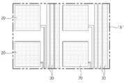
종래의 매트릭스 스위칭 타입의 터치패널은 도 1에서 도시하는 바와 같이 투명전극이 패터닝되어 터치패드(20) 및 신호라인(30)을 형성함에 따라, 기판(10)의 가시영역(A1) 상에는 투명전극이 존재하는 영역과 투명전극이 존재하지 않는 영역으로 구분된다.1, a transparent electrode is patterned to form a
그런데, 투명전극이 존재하는 영역과 투명전극이 존재하지 않는 영역은 투과율 차이, 반사율 차이, 색상 차 등에 의해 패터닝 자국, 즉 투명전극이 존재하는 영역이 시각적으로 드러나는 문제가 있다.However, the region where the transparent electrode exists and the region where the transparent electrode does not exist have a problem that the patterning traces, that is, the region where the transparent electrode exists are visually revealed due to the difference in transmittance, the difference in reflectivity, and the color difference.
최근 이와 같은 터치 스크린 패널에 있어서 투명전극이 존재하는 영역과 존재하지 않는 영역 사이의 시각적 차이를 개선하기 위하여 투명전극과 투명전극이 존재하지 않는 기판 부위를 덮는 코팅층을 구비하도록 하고 있다.In recent years, in order to improve the visual difference between a region where a transparent electrode exists and a region where a transparent electrode does not exist, a coating layer covering a portion of the substrate where the transparent electrode and the transparent electrode do not exist is provided.
그러나 코팅층을 추가하는 것은 비용 및 공정 증가의 원인이 될 뿐만 아니라, 코팅층을 추가하더라도 매트릭스 스위칭 타입의 터치패널은 여러 개의 신호라인(30)이 기판(10)의 가시영역(A1) 내에서 나란한 직선형태로 배치되므로 쉽게 시인되는 문제가 있다.However, not only does adding a coating layer cause cost and process increase, but even if a coating layer is added, a matrix switching type touch panel can be used in which a plurality of
또한, 터치패드(20)와 터치구동회로(40)를 각각 연결하는 신호라인(30)은 터치구동회로(40)와 터치패드(20)의 거리가 먼 경우, 즉 신호라인(30)의 배선길이가 길어질수록 저항과 기생용량이 증가한다. 따라서, 신호라인(30)은 도 2와 같이 배선길이가 길어질수록 폭이 증가하는 형태로 디자인된다. 그런데, 이러한 경우에는 일부 영역에서 신호라인(30)의 경계가 다른 영역에 비해 조밀하게 배치되어 쉽게 시인되는 구조적인 문제점이 있다.The
또한, 터치패드의 신호전극의 라인과 액정패널의 화소전극의 라인의 방향이 일치할 경우, 도 3과 같이 평행한 2개의 일정한 간격을 갖는 패턴이 겹쳐지면서 광학적 결함이 발생한다. 즉, 소정의 간격(D)을 갖는 선무늬가 표시되는 모아레(moire) 현상으로 인해 화면품위가 저하되는 문제점이 있다.When the lines of the signal electrodes of the touch pad and the lines of the pixel electrodes of the liquid crystal panel coincide with each other, optical defects are generated by overlapping patterns having two parallel intervals, as shown in Fig. That is, there is a problem that the quality of the screen is degraded due to a moire phenomenon in which a line pattern having a predetermined interval D is displayed.
따라서, 본 발명의 목적은 이와 같은 종래의 문제점을 해결하기 위한 것으로서, 투명전극이 존재하는 영역과 투명전극이 존재하지 않는 영역의 경계가 시인되는 것을 방지하는 것과 동시에, 터치패널의 투명전극에 의해 모아레 현상이 발생하는 것을 방지할 수 있는 매트릭스 스위칭 타입 터치패널을 제공함에 있다.SUMMARY OF THE INVENTION It is therefore an object of the present invention to provide a touch panel which is capable of preventing a boundary between a region where a transparent electrode exists and a region where a transparent electrode is not present from being visually recognized, And a matrix switching type touch panel capable of preventing a moire phenomenon from occurring.
또한, 단위전극간의 상하, 좌우 방향의 경계가 시인되는 것을 방지할 수 있는 매트릭스 스위칭 타입 터치패널을 제공함에 있다.It is another object of the present invention to provide a matrix switching type touch panel capable of preventing the boundary between the unit electrodes from being viewed in the vertical and horizontal directions.
상기 목적은, 본 발명에 따라, 기판상의 가시영역에 도트 매트릭스 형태로 상호 이격 배치되는 터치패드와, 상기 터치패드 사이의 이격공간에 배치되어 터치패드와 비가시영역의 터치구동회로를 각각 연결하는 신호라인을 포함하는 매트릭스 스위칭 타입 터치패널에 있어서, 투명전극재질로 이루어져 기판상의 가시영역내에 배열되는 단위전극;과, 각 터치패드에 대응하는 영역에 설정되는 터치패드영역;과, 각 신호라인에 대응하는 영역에 설정되는 신호라인영역; 및, 상기 터치패드영역과 신호라인영역에 각각 배치되는 다수의 단위전극들을 전기적으로 연결하여 터치패드와 신호라인을 구성하는 투명전극재질의 브릿지;를 포함하며, 상기 단위전극은 신호라인과 나란한 제1축에 대하여 지그재그 형태로 배열되어 이루어지는 매트릭스 스위칭 타입 터치패널에 의해 달성된다.According to an aspect of the present invention, there is provided a display device comprising: a touch pad disposed in a visible matrix area on a substrate, the touch pad being spaced apart from each other by a dot matrix; And a signal line, wherein the touch panel includes a unit electrode formed of a transparent electrode material and arranged in a visible region on the substrate, a touch pad region set in an area corresponding to each touch pad, A signal line region set in a corresponding region; And a bridge of a transparent electrode material electrically connecting a plurality of unit electrodes arranged in the touch pad area and the signal line area to constitute a touch pad and a signal line, And is arranged in a zigzag manner with respect to one axis.
여기서, 상기 단위전극은 제1축에 대하여 제1방향으로 경사배치되는 제1직선구간과, 제1축을 기준으로 제1직선구간과 대칭되는 제2방향으로 경사배치되는 제2직선구간이 교대로 반복되도록 배열되는 것이 바람직하다.Here, the unit electrode may include a first linear section inclined with respect to the first axis in a first direction and a second linear section inclined with respect to the first axis in a second direction symmetrical to the first linear section, It is preferable that they are arranged to be repeated.
또한, 상기 제1방향과 제2방향은 제1축에 대하여 양측으로 10도 내지 20도의 범위로 설정되는 것이 바람직하다.In addition, it is preferable that the first direction and the second direction are set in the range of 10 degrees to 20 degrees on both sides with respect to the first axis.
또한, 상기 브릿지는 단위전극과 동일 레이어 상에 형성되는 것을 특징으로 하는 것이 바람직하다.It is preferable that the bridge is formed on the same layer as the unit electrode.
또한, 상기 단위전극은 적어도 양측면에 다수의 돌기가 형성되고, 상기 다수의 돌기는 이웃하는 단위전극의 돌기와 서로 엇갈리게 배치되는 것을 특징으로 하는 것이 바람직하다.The unit electrode may have a plurality of protrusions formed on at least both sides thereof, and the plurality of protrusions may be offset from the protrusions of neighboring unit electrodes.
또한, 상기 신호라인과 교차하는 방향으로 단위전극들을 연결하는 브릿지는 이웃하는 한 쌍의 단위전극에 마련되는 다수의 돌기 중 적어도 어느 하나의 돌기로부터 연장 형성되는 것이 바람직하다.The bridge connecting the unit electrodes in a direction crossing the signal line may be extended from at least one of the plurality of protrusions provided on the pair of adjacent unit electrodes.
또한, 상기 브릿지는 신호라인과 교차하는 방향에 대하여 이웃하는 브릿지와 서로 엇갈리게 배치되는 것을 것이 바람직하다.It is also preferable that the bridge is arranged to be offset from neighboring bridges in a direction crossing the signal lines.
또한, 상기 단위전극의 단부는 신호라인과 교차하는 방향에 대하여 이웃하는 단위전극의 단부와 서로 엇갈리게 배치되는 것이 바람직하다.It is preferable that the ends of the unit electrodes are disposed to be offset from the ends of the unit electrodes adjacent to each other in the direction crossing the signal lines.
또한, 상기 신호라인은 터치패널과 터치구동회로 사이의 배선 길이에 따라 저항을 감소시킬 수 있도록 일렬로 연결된 적어도 2개 이상의 단위 신호라인이 전기적으로 연결되는 것이 바람직하다.In addition, at least two or more unit signal lines connected in series may be electrically connected to reduce the resistance of the signal line according to the wiring length between the touch panel and the touch driving circuit.
또한, 상기 2개 이상의 단위 신호라인은 비가시영역 내에서 신호라인과 터치구동회로를 각각 연결하는 연결라인이 서로 전기적으로 연결되는 것이 바람직하다.Preferably, the at least two unit signal lines are electrically connected to each other through connection lines connecting the signal lines and the touch driving circuits in the non-visible region.
또한, 상기 2개 이상의 단위 신호라인은 가시영역 내에서 다수의 브릿지에 의해 전기적으로 연결되는 것이 바람직하다.Preferably, the two or more unit signal lines are electrically connected by a plurality of bridges in a visible region.
본 발명에 따르면, 투명전극이 존재하는 영역과 투명전극이 존재하지 않는 영역의 경계가 시인되는 것을 방지하는 것과 동시에, 터치패널의 투명전극에 의해 모아레 현상이 발생하는 것을 방지할 수 있는 매트릭스 스위칭 타입 터치패널이 제공된다.According to the present invention, it is possible to prevent a boundary between a region where a transparent electrode exists and a region where a transparent electrode is not present from being visible, and a matrix switching type A touch panel is provided.
또한, 또한, 단위전극간의 상하, 좌우 방향의 경계가 시인되는 것을 방지할 수 있는 매트릭스 스위칭 타입 터치패널이 제공된다.Furthermore, there is also provided a matrix switching type touch panel capable of preventing the boundaries between the unit electrodes from being viewed in the vertical and horizontal directions.
도 1은 종래 매트릭스 스위칭 타입 터치패널의 평면 구성도,
도 2는 도 1의 "A"부분의 확대도,
도 3은 모아레 현상을 나타내는 도면,
도 4는 본 발명 매트릭스 스위칭 타입 터치패널의 평면 구성도,
도 5는 도 4의 주요부분의 확대도,
도 6 내지 도 8은 본 발명의 매트릭스 스위칭 타입 터치패널의 형성과정을 나타내는 도면,
도 9는 본 발명 매트릭스 스위칭 타입 터치패널에 따른 신호라인의 부분확대도이고,
도 10은 본 발명 매트릭스 스위칭 타입 터치패널에 따른 단위전극의 변형 예이다.1 is a plan view of a conventional matrix switching type touch panel,
2 is an enlarged view of a portion "A" in Fig. 1,
3 is a view showing a moire phenomenon,
4 is a plan view of the matrix switching type touch panel of the present invention,
Fig. 5 is an enlarged view of the main part of Fig. 4,
6 to 8 are views showing a process of forming the matrix switching type touch panel of the present invention,
9 is a partially enlarged view of a signal line according to the matrix switching type touch panel of the present invention,
10 is a modification of the unit electrode according to the present invention matrix switching type touch panel.
설명에 앞서, 여러 실시예에 있어서, 동일한 구성을 가지는 구성요소에 대해서는 동일한 부호를 사용하여 대표적으로 제1실시예에서 설명하고, 그 외의 실시예에서는 제1실시예와 다른 구성에 대해서 설명하기로 한다.Prior to the description, components having the same configuration are denoted by the same reference numerals as those in the first embodiment. In other embodiments, configurations different from those of the first embodiment will be described do.
이하, 첨부한 도면을 참조하여 본 발명의 제1실시예에 따른 매트릭스 스위칭 타입 터치패널에 대하여 상세하게 설명한다.Hereinafter, a matrix switching type touch panel according to a first embodiment of the present invention will be described in detail with reference to the accompanying drawings.
첨부도면 중 도 4는 본 발명 매트릭스 스위칭 타입 터치패널의 평면 구성도이고, 도 5는 도 4의 주요부분의 확대도이다.4 is a plan view of the matrix switching type touch panel of the present invention, and FIG. 5 is an enlarged view of a main portion of FIG.
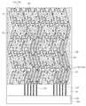
상기 도면에서 도시하는 바와 같은 본 발명은, 기판(100)상의 가시영역(A1)에 도트 매트릭스 형태로 상호 이격 배치되는 터치패드(120)와, 상기 터치패드(120) 사이의 이격공간에 배치되어 터치패드(120)와 비가시영역(A2)의 터치구동회로(150)를 각각 연결하는 신호라인(130)을 포함하는 매트릭스 스위칭 타입 터치패널에 관한 것이다.The present invention as shown in the drawings is characterized in that it includes a
이러한 본 발명 매트릭스 스위칭 타입 터치패널은, 투명전극재질로 이루어져 기판상의 가시영역(A1)내에 배열되는 단위전극(110)과, 가시영역(A1) 중 터치패드(120)에 대응하는 영역에 각각 설정되는 터치패드영역(TA)과, 신호라인(130)에 대응하는 영역에 각각 정되는 신호라인영역(SA) 및, 상기 터치패드영역(TA)과 신호라인영역(SA)에 각각 배치되는 다수의 단위전극(110)들을 전기적으로 연결하여 터치패드(120)와 신호라인(130)을 구성하는 투명전극재질의 브릿지(140)를 포함하여 구성된다.The matrix switching type touch panel of the present invention comprises a
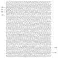
상기 단위전극(110)은 직사각형의 투명전극재질로 이루어져 신호라인과 나란한 제1축(도 5에서 Y축으로 표시)에 대하여 지그재그 형태로 배열된다.The
즉, 상기 단위전극(110)은 제1축(Y)에 대하여 제1방향으로 경사배치되는 제1직선구간과, 제1축(Y)을 기준으로 제1직선구간과 대칭되는 제2방향으로 경사배치되는 제2직선구간이 교대로 반복되도록 배열되고, 상기 제1방향과 제2방향은 제1축(Y)에 대하여 양측으로 10도 내지 20도의 범위로 설정된다. 여기서, 경사각도가 0~9도로 설정되는 경우에는 모아레 무늬의 간격이 사람의 눈으로 확인할 수 있는 150㎛ 이상이 되어 모아레 무늬가 시인된다. 또한, 20도를 초과하는 경우에는 지그재그 형태로 배열되는 단위전극(110)과 가시영역(A1)의 테두리 사이에 터치 불가능영역이 커지게 된다.That is, the
단위전극(110)의 양 측면에는 다수의 돌기(112)가 이격 배치된다. 또한, 신호라인(130)과 직교하는 제2축(도 5에서 X축으로 표시) 방향으로 이웃하는 한 쌍의 단위전극(110)들의 서로 마주하는 면에 형성된 돌기(112)들은 맞은편의 돌기(112)와 서로 엇갈리게 배치되고, 직사각형 단위전극(110)의 외측면 중 단변으로 이루어진 단부는 신호라인(130)과 교차하는 제2축(X) 방향에 대하여 이웃하는 단위전극(110)의 단부와 서로 엇갈리게 배치된다.On both side surfaces of the
상기 브릿지(140)는 단위전극(110)과 동일한 투명전극재질로 이루어지고, 단위전극(110)의 형성과정에서 함께 형성되어 단위전극(110)과 동일한 레이어상에 배치된다. 이러한 브릿지(140)는 이웃하는 한 쌍의 단위전극(110)에 마련되는 다수의 돌기(112) 중 적어도 어느 하나의 돌기(112)로부터 연장되어 제2축(X) 방향으로 이웃하는 단위전극(110)과 전기적으로 연결된다. 또한, 상기 브릿지(140)는 제2축(X) 방향에 대하여 이웃하는 브릿지(140)와 서로 엇갈리게 배치된다.
The
상기와 같이 구성되는 본 발명의 매트릭스 스위칭 타입 터치패널의 제1실시예에 따르면, 단위전극(110)은 제1축(Y)에 대해 경사배치되며, 터치패널과 적층 구성되는 확산필름 또는 TFT 어레이 패널의 패턴과 소정각도 엇갈리게 되므로 모아레 현상을 방지할 수 있다.According to the first embodiment of the matrix switching type touch panel of the present invention configured as described above, the
또한, 단위전극(110)은 제1방향으로 경사배치되는 제1직선구간과, 제1축(Y)을 기준으로 제1직선구간과 대칭되는 제2방향으로 경사배치되는 제2직선구간이 교대로 반복되어 제1축(Y)을 따라 지그재그 형태로 배열되므로, 가시영역(A1)의 테두리에 발생할 수 있는 터치 불가능영역을 최소화할 수 있다.In addition, the
또한, 기판의 가시영역(A1)에 동일한 형상을 갖는 단위전극(110)을 가로세로 방향으로 배열하되, 단위전극(110)의 단변에 대응하는 단부가 이웃하는 단위전극(110)의 단부와 신호라인(130)과 교차하는 제2축(X) 방향에 대하여 서로 엇갈리도록 한다.The
이러한 배치구조에 따르면, 단위전극(110)이 존재하는 영역과 단위전극(110)이 존재하지 않는 영역 사이의 투과율 차이, 반사율 차이, 색상 차 등에 의해 패터닝 자국, 즉 상기 투명전극이 존재하는 영역이 존재하지 않는 영역과 시각적으로 구분되는 것을 방지할 수 있다.According to this arrangement, the patterning traces, that is, the regions where the transparent electrodes exist exist between the regions where the
또한, 이러한 직사각형 단위전극(110)은, 신호라인(130)과 나란한 제1축(Y) 방향에 대하여 단위전극(110)의 장변에 대응하는 측면부에 다수의 돌기(112)들이 형성되어 있으므로, 단위전극(110)의 측면부 경계라인이 시인되는 것을 방지할 수 있다.Since the plurality of
또한, 단위전극(110) 사이의 좌,우측 이격공간은, 이격공간을 사이에 두고 제2축(X) 방향으로 이웃하는 양측의 단위전극(110)의 돌기(112)들이 서로 엇갈리게 배치되므로 좌,우로 배치되는 단위전극(110) 사이의 이격공간이 시인되는 것을 방지할 수 있다.Since the
뿐만 아니라, 제1축(Y) 방향으로 이격되어 있는 단위전극(110) 사이의 상,하측 단부는 제2축(X) 방향으로 이웃하는 단위전극(110)의 단부와 서로 엇갈리게 배치되므로 상,하로 배치되는 단위전극(110) 사이의 이격공간이 시인되는 것을 방지할 수 있다.The upper and lower ends of the
즉, 상기와 같은 단위전극(110)의 배치구조에 따르면, 단위전극(110)이 형성된 부분과 형성되지 않은 부분이 시각적으로 구분되는 것이 방지되고, 단위전극(110)사이의 이격공간이 제2축(X), 제1축(Y) 방향으로 직선으로 배치되는 것이 방지되므로, 가시영역(A1) 내에서 단위전극(110)은 물론 단위전극(110) 사이의 이격공간이 시인되는 것을 방지할 수 있다.
In other words, according to the arrangement structure of the
한편, 상기와 같은 본 발명의 제1실시예에 따른 단위전극(110)의 배치구조로부터 터치패드(120)와 신호라인(130)을 형성하는 과정을 도면을 참조하여 살펴보면 다음과 같다.A process of forming the
첨부도면 중 도 5 내지 도 7은 본 발명의 매트릭스 스위칭 타입 터치패널의 형성과정을 나타내는 도면들이다.5 to 7 are views showing a process of forming a matrix switching type touch panel according to the present invention.
본 실시예에 따른 매트릭스 스위칭 타입 터치패널은, 도 1과 같이 터치패드(120)가 도트 매트릭스 형태로 상호 이격 배치되고, 각 터치패드(120)와 비가시영역(A2)에 배치되는 터치구동회로(150)를 연결하는 다수의 신호라인(130)이 터치패드(120) 사이의 이격공간 내에 배치된다.The matrix type touch panel according to the present embodiment includes
즉, 도 5와 같이 가시영역(A1) 내에 다수의 단위전극(110)은 제1축(Y)에 대하여 제1방향으로 경사배치되는 제1직선구간과, 제1축(Y)을 기준으로 제1직선구간과 대칭되는 제2방향으로 경사배치되는 제2직선구간이 교대로 반복되어 제1축(Y)을 따라 지그재그 형태로 배열된다.That is, as shown in FIG. 5, a plurality of
또한, 상기와 같은 단위전극(110)을 기반으로 하여 터치패드(120)와 신호라인(130)을 형성하기 위해서, 도 6과 같이 매트릭스 스위칭 타입 터치패널의 각 터치패드(120)에 대응하는 영역을 터치패드영역(TA)으로 설정하고, 각 신호라인(130)에 대응하는 영역을 신호라인영역(SA)으로 설정한다.In order to form the
구체적으로, 터치패드영역(TA)은 터치패드에 대응하는 다수의 단위전극(110)들을 포함하는 테두리로 설정된다. 이때, 다수의 단위전극(110)의 단부는 제2축(X) 방향으로 이웃하는 단위전극의 단부와 서로 어긋나게 배치되어 있으므로, 제1축(Y) 방향으로 배열된 상,하측 터치패드영역(TA) 사이의 경계는 불규칙한 라인 형태로 설정된다.Specifically, the touch pad area TA is set to a frame including a plurality of
또한, 신호라인영역(SA)은 각 터치패드영역(TA)과 비가시영역(A2)에 배치되는 터치구동회로(150)를 연결하도록 좌우 터치패드영역(TA) 사이의 이격공간 내에 서로 제1축(Y) 방향으로 배치되는 것으로서, 각각의 터치패드영역(TA)의 위치에 대응하여 서로 다른 길이로 이루어지며, 상단부는 해당 터치패드영역(TA)과 접하도록 설정된다.The signal line area SA is connected to the first and second touch pad areas TA and TA to connect the
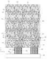
상기와 같이 터치패드영역(TA)과 신호라인영역(SA)이 설정된 이후에는, 투명전극재질로 이루어지는 브릿지(140)를 단위전극(110) 사이에 배치하여 터치패드영역(TA)과 신호라인영역(SA) 내에 배치되는 단위전극(110)들을 서로 전기적으로 연결한다.After the touch pad area TA and the signal line area SA are set as described above, a
즉, 도 7 및 도 4와 같이, 제2축(X) 방향으로 배열된 단위전극(110)들을 연결함에 있어서는 단위전극(110)의 장변에 형성된 돌기(112)와 제2축(X) 방향으로 이웃하는 단위전극(110)의 사이에 투명전극 재질의 브릿지(140)를 배치하여 좌우의 단위전극(110)들을 전기적으로 연결한다.7 and FIG. 4, when connecting the
이때, 제2축(X) 방향으로 배열되는 다수의 브릿지(140)들은 이웃하는 브릿지(140)와 서로 엇갈리도록 배치함으로써, 일렬로 배치되는 브릿지(140)에 의해 시인성이 증가하는 것을 방지한다.At this time, the plurality of
또한, 제1축(Y) 방향을 따라 지그재그 형태로 배열된 다수의 단위전극(110)들을 연결함에 있어서는 단위전극(110)의 단변과 이웃하는 단위전극(110)의 단변 사이에 투명전극 재질의 브릿지(140)를 배치하여 상하의 단위전극(110)들을 전기적으로 연결한다.When a plurality of
상기와 같이 터치패드영역(TA)과 신호라인영역(SA) 내에 배치되는 단위전극(110)을 각각 브릿지(140)로 연결하여 터치패드(120)와 신호라인(130)을 구성한다.The
또한, 터치패드(120)와 이에 대응하는 신호라인(130)의 상단부를 각각 브릿지(140)로 연결하고, 브릿지(140)와 동일한 재질로 이루어져 비가시영역(A2)에 배치되는 연결라인(132)으로 신호라인(130)의 하단부를 터치구동회로(150)와 연결한다.The upper portion of the
한편, 본 실시예에서는 발명의 이해를 돕기 위해서 단위전극(110)과 구분되는 브릿지(140)를 이용하여 다수의 단위전극(110)들을 전기적으로 연결하고, 연결라인(132)을 이용하여 신호라인(130)과 터치구동회로(150)를 전기적으로 연결하는 것으로 설명하였으나, 브릿지(140)와 연결라인(132)은 단위전극(110)을 패터닝하는 과정에서 단위전극(110)과 함께 일체로 형성하는 것이 바람직하다.In order to facilitate understanding of the present invention, a plurality of
또한, 본 실시예에서는 터치패드(120)와 신호라인(130)을 동일한 레이어에 배치하고, 터치패드(120)와 신호라인(130)을 브릿지(140)로 연결하여 싱글 레이어 타입 터치패널을 구성하는 것으로 예를 들어 설명하였으나, 터치패드(120)와 신호라인(130)을 상부레이어와 하부레이어로 배치한 다음 브릿지(140)로 연결하여 더블 레이어 타입 터치패널로 구성하는 것도 가능할 것이다.
In this embodiment, the
첨부도면 중 도 8은 본 발명 매트릭스 스위칭 타입 터치패널에 따른 신호라인(130)의 부분확대도이다.8 is a partial enlarged view of a
본 발명의 매트릭스 스위칭 타입 터치패널에 따른 신호라인(130)의 변형예에 따르면, 신호라인(130)은 터치패드(120)과 터치구동회로(150) 사이의 배선 길이에 따라 저항을 감소시킬 수 있도록 일렬로 배치된 다수의 단위 신호라인(130')중 2개 이상의 단위 신호라인(130')을 전기적으로 연결하여 구성될 수 있다. 여기서, 단위 신호라인(130')은 일렬로 배치되는 다수의 단위전극(110)이 브릿지(140)에 의해 연결되어 하나의 라인형태로 이루어지는 것도 가능하다.According to a modification of the
즉, 도 8에서 도시하는 바와 같이 일렬로 배치된 다수의 단위 신호라인(130')은, 비가시영역(A2) 내에서 신호라인(130)과 터치구동회로(150)를 각각 연결하는 연결라인(132)이 서로 전기적으로 연결되어 신호라인(130)의 면적을 증가시킴으로써, 신호라인(130)의 배선길이가 길어지더라도 저항 및 기생용량이 증가하는 것을 방지할 수 있다.8, a plurality of unit signal lines 130 'arranged in a line form a connection line (not shown) connecting the
특히, 상기와 같은 신호라인(130)은 동일한 형태를 갖는 여러 개의 단위 신호라인(130')을 비가시영역(A2)에서 전기적으로 연결하는 것이므로, 신호라인(130)의 면적을 증가시키더라도 종래와 같이 신호라인(130)의 폭의 증가나 간격의 변화가 나타나지 않으므로, 신호라인(130)이 시각적으로 드러나는 것을 방지할 수 있다.In particular, the
한편, 본 실시예에서는 2개 이상의 단위 신호라인(130')이 비가시영역(A2)에서 전기적으로 연결되는 것으로 설명하였으나, 2개 이상의 단위 신호라인(130')이 가시영역(A1) 내에서 다수의 브릿지(140)에 의해 전기적으로 연결되도록 구성하는 것도 가능할 것이다. 이때, 상기 2개 이상의 단위 신호라인(130')을 연결하는 다수의 브릿지(140)는 앞서 설명한 바와 같이 제2축(X) 방향에 대하여 서로 엇갈리도록 배치하는 것이 바람직할 것이다.
Although two or more unit signal lines 130 'are electrically connected in the non-visible region A2 in the present embodiment, two or more unit signal lines 130' may be formed in the visible region A1 It may be configured to be electrically connected by a plurality of
첨부도면 중 도 9는 본 발명 매트릭스 스위칭 타입 터치패널에 따른 단위전극(110)의 변형 예를 나타낸 것이다.9 is a modification of the
본 발명에 따른 단위전극(110)의 변형 예에 따르면, 단위전극(110)의 양측에 형성되는 돌기(112)를 도 9의 (a)와 같이 삼각형으로 구성하거나, 도 9의 (b)와 같이 반원형으로 구성하는 것도 가능하다.According to a modification of the
물론, 이러한 삼각형 또는 반원형의 돌기(112) 역시 제1실시예와 마찬가지로 이웃하는 단위전극(110)의 돌기(112)와 신호라인(130)과 교차하는 방향에 대하여 엇갈리게 배치하여야 할 것이다.
Of course, the triangular or
본 발명의 권리범위는 상술한 실시예에 한정되는 것이 아니라 첨부된 특허청구범위 내에서 다양한 형태의 실시예로 구현될 수 있다. 특허청구범위에서 청구하는 본 발명의 요지를 벗어남이 없이 당해 발명이 속하는 기술 분야에서 통상의 지식을 가진 자라면 누구든지 변형 가능한 다양한 범위까지 본 발명의 청구범위 기재의 범위 내에 있는 것으로 본다.The scope of the present invention is not limited to the above-described embodiments, but may be embodied in various forms of embodiments within the scope of the appended claims. It will be understood by those skilled in the art that various changes in form and details may be made therein without departing from the spirit and scope of the present invention as defined by the appended claims.
110:단위전극, 112:돌기, 120:터치패드,
130:신호라인, 130':단위신호라인, 132:연장라인,
140:브릿지, 150:터치구동회로,
TA:터치패드영역, SA:신호라인영역,
A1:가시영역, A2:비가시영역110: unit electrode, 112: projection, 120: touch pad,
130: signal line, 130 ': unit signal line, 132: extension line,
140: bridge, 150: touch driving circuit,
TA: touch pad area, SA: signal line area,
A1: visible region, A2: invisible region
Claims (11)
Translated fromKorean투명전극재질로 이루어져 기판상의 가시영역내에 배열되는 단위전극;
각 터치패드에 대응하는 영역에 설정되는 터치패드영역;
각 신호라인에 대응하는 영역에 설정되는 신호라인영역; 및,
상기 터치패드영역과 신호라인영역에 각각 배치되는 다수의 단위전극들을 전기적으로 연결하여 터치패드와 신호라인을 구성하는 투명전극재질의 브릿지;를 포함하며,
상기 단위전극은 신호라인과 나란한 제1축에 대하여 지그재그 형태로 배열되어 이루어지는 매트릭스 스위칭 타입 터치패널.And a signal line connecting the touch pad and the touch driving circuit in a non-visible region, the touch pad being disposed in a spaced space between the touch pads, In the panel,
A unit electrode formed of a transparent electrode material and arranged in a visible region on the substrate;
A touch pad area set in an area corresponding to each touch pad;
A signal line region set in an area corresponding to each signal line; And
And a bridge of a transparent electrode material constituting a touch pad and a signal line by electrically connecting a plurality of unit electrodes respectively arranged in the touch pad area and the signal line area,
Wherein the unit electrodes are arranged in a zigzag manner with respect to a first axis parallel to the signal lines.
상기 단위전극은 제1축에 대하여 제1방향으로 경사배치되는 제1직선구간과, 제1축을 기준으로 제1직선구간과 대칭되는 제2방향으로 경사배치되는 제2직선구간이 교대로 반복되도록 배열되는 매트릭스 스위칭 타입 터치패널.The method according to claim 1,
Wherein the unit electrode includes a first straight line section inclined in the first direction with respect to the first axis and a second straight line section inclined in the second direction symmetrical with respect to the first straight section with respect to the first axis are alternately repeated Matrix switching type touch panels arranged.
상기 제1방향과 제2방향은 제1축에 대하여 양측으로 10도 내지 20도의 범위로 설정되는 매트릭스 스위칭 타입 터치패널.3. The method of claim 2,
Wherein the first direction and the second direction are set in a range of 10 degrees to 20 degrees on both sides with respect to the first axis.
상기 브릿지는 단위전극과 동일 레이어 상에 형성되는 매트릭스 스위칭 타입 터치패널.The method according to claim 1,
Wherein the bridge is formed on the same layer as the unit electrode.
상기 단위전극은 적어도 양측면에 다수의 돌기가 형성되고,
상기 다수의 돌기는 이웃하는 단위전극의 돌기와 서로 엇갈리게 배치되는 매트릭스 스위칭 타입 터치패널.5. The method of claim 4,
The unit electrode has a plurality of protrusions formed on at least both sides thereof,
Wherein the plurality of protrusions are arranged to be offset from the protrusions of neighboring unit electrodes.
상기 신호라인과 교차하는 방향으로 단위전극들을 연결하는 브릿지는 이웃하는 한 쌍의 단위전극에 마련되는 다수의 돌기 중 적어도 어느 하나의 돌기로부터 연장 형성되는 매트릭스 스위칭 타입 터치패널.6. The method of claim 5,
Wherein the bridge connecting the unit electrodes in a direction crossing the signal line is extended from at least one of a plurality of protrusions provided on a pair of neighboring unit electrodes.
상기 브릿지는 신호라인과 교차하는 방향에 대하여 이웃하는 브릿지와 서로 엇갈리게 배치되는 매트릭스 스위칭 타입 터치패널.The method according to claim 6,
Wherein the bridge is arranged to be staggered with neighboring bridges in a direction crossing the signal lines.
상기 단위전극의 단부는 신호라인과 교차하는 방향에 대하여 이웃하는 단위전극의 단부와 서로 엇갈리게 배치되는 매트릭스 스위칭 타입 터치패널.The method according to claim 1,
Wherein the end portions of the unit electrodes are disposed to be offset from the end portions of the neighboring unit electrodes in a direction crossing the signal lines.
상기 신호라인은 터치패널과 터치구동회로 사이의 배선 길이에 따라 저항을 감소시킬 수 있도록 일렬로 연결된 적어도 2개 이상의 단위 신호라인이 전기적으로 연결되는 매트릭스 스위칭 타입 터치패널.The method according to claim 1,
Wherein the signal line is electrically connected to at least two or more unit signal lines connected in series so as to reduce the resistance according to a wiring length between the touch panel and the touch driving circuit.
상기 2개 이상의 단위 신호라인은 비가시영역 내에서 신호라인과 터치구동회로를 각각 연결하는 연결라인이 서로 전기적으로 연결되는 매트릭스 스위칭 타입 터치패널.10. The method of claim 9,
And the connection lines connecting the signal lines and the touch driving circuits are electrically connected to each other within the invisible region of the at least two unit signal lines.
상기 2개 이상의 단위 신호라인은 가시영역 내에서 다수의 브릿지에 의해 전기적으로 연결되는 매트릭스 스위칭 타입 터치패널.10. The method of claim 9,
Wherein the at least two unit signal lines are electrically connected by a plurality of bridges in a visible region.
Priority Applications (5)
| Application Number | Priority Date | Filing Date | Title |
|---|---|---|---|
| KR1020140022502AKR101527320B1 (en) | 2014-02-26 | 2014-02-26 | Matrix switching type Touch panel |
| TW103144040ATWI630531B (en) | 2014-02-26 | 2014-12-17 | Matrix switching type touch panel |
| CN201410827193.8ACN104866131B (en) | 2014-02-26 | 2014-12-25 | Inverse problem formula touch panel |
| JP2014265549AJP6322135B2 (en) | 2014-02-26 | 2014-12-26 | Matrix switching type touch panel |
| US14/587,038US9857926B2 (en) | 2014-02-26 | 2014-12-31 | Matrix switching type touch panel comprising unit electrodes connected by bridges |
Applications Claiming Priority (1)
| Application Number | Priority Date | Filing Date | Title |
|---|---|---|---|
| KR1020140022502AKR101527320B1 (en) | 2014-02-26 | 2014-02-26 | Matrix switching type Touch panel |
Publications (1)
| Publication Number | Publication Date |
|---|---|
| KR101527320B1true KR101527320B1 (en) | 2015-06-09 |
Family
ID=53504086
Family Applications (1)
| Application Number | Title | Priority Date | Filing Date |
|---|---|---|---|
| KR1020140022502AActiveKR101527320B1 (en) | 2014-02-26 | 2014-02-26 | Matrix switching type Touch panel |
Country Status (5)
| Country | Link |
|---|---|
| US (1) | US9857926B2 (en) |
| JP (1) | JP6322135B2 (en) |
| KR (1) | KR101527320B1 (en) |
| CN (1) | CN104866131B (en) |
| TW (1) | TWI630531B (en) |
Cited By (3)
| Publication number | Priority date | Publication date | Assignee | Title |
|---|---|---|---|---|
| CN107533404A (en)* | 2015-06-22 | 2018-01-02 | 株式会社藤仓 | Wiring body, wiring substrate, and touch sensor |
| KR20180127084A (en)* | 2017-05-19 | 2018-11-28 | 동우 화인켐 주식회사 | Touch sensing electrode structure and touch sensor including the same |
| KR102200971B1 (en)* | 2019-12-27 | 2021-01-11 | 알에스오토메이션주식회사 | Light-receiving element of Optical Encoder |
Families Citing this family (4)
| Publication number | Priority date | Publication date | Assignee | Title |
|---|---|---|---|---|
| CN103186306A (en)* | 2013-03-26 | 2013-07-03 | 北京京东方光电科技有限公司 | Capacitive touch screen and display device |
| KR102536878B1 (en)* | 2016-01-26 | 2023-05-26 | 삼성디스플레이 주식회사 | Touch panel and display apparatus including the same |
| CN109388294B (en)* | 2017-08-11 | 2021-01-22 | 京东方科技集团股份有限公司 | Touch panel and manufacturing method thereof, and touch display device |
| CN113093931B (en)* | 2020-01-08 | 2023-12-01 | 京东方科技集团股份有限公司 | electronic device |
Citations (4)
| Publication number | Priority date | Publication date | Assignee | Title |
|---|---|---|---|---|
| KR20100028277A (en)* | 2008-09-04 | 2010-03-12 | 삼성전기주식회사 | Tactile sensor |
| KR101202552B1 (en)* | 2012-03-11 | 2012-11-19 | (주)이미지스테크놀로지 | A improved touch location sensor panel having one-layered structure |
| KR20130027747A (en)* | 2011-09-08 | 2013-03-18 | 삼성전기주식회사 | Touch pannel |
| KR20140112626A (en)* | 2013-03-12 | 2014-09-24 | 주식회사 실리콘웍스 | Touch panel |
Family Cites Families (19)
| Publication number | Priority date | Publication date | Assignee | Title |
|---|---|---|---|---|
| JP4202110B2 (en)* | 2002-03-26 | 2008-12-24 | シャープ株式会社 | Display device, driving method, and projector device |
| TWI274273B (en)* | 2005-06-15 | 2007-02-21 | Wintek Corp | Touch panel circuit layout for avoiding moire |
| JP5174575B2 (en)* | 2008-07-31 | 2013-04-03 | グンゼ株式会社 | Touch panel |
| JP5174745B2 (en)* | 2009-06-09 | 2013-04-03 | グンゼ株式会社 | Touch switch |
| KR101633034B1 (en)* | 2009-10-23 | 2016-06-24 | 삼성디스플레이 주식회사 | Touch substrate, method of manufacturing the same and display apparatus having the same |
| US9851829B2 (en)* | 2010-08-27 | 2017-12-26 | Apple Inc. | Signal processing for touch and hover sensing display device |
| KR101704536B1 (en)* | 2010-10-08 | 2017-02-09 | 삼성전자주식회사 | Touch Panel type of Slim and Portable Device including the same |
| US20120153970A1 (en) | 2010-12-21 | 2012-06-21 | Qualcomm Mems Technologies, Inc. | Capacitive touch sensing devices and methods of manufacturing thereof |
| KR20120100488A (en)* | 2011-03-04 | 2012-09-12 | 하이디스 테크놀로지 주식회사 | Capacitance touch panel and the method thereof |
| KR101165456B1 (en)* | 2011-03-07 | 2012-07-12 | 이성호 | Capacitive type touch detecting means, method and touch screen panel using voltage changing phenomenon, and display device embedding said the capacitive type touch screen panel |
| KR101301408B1 (en)* | 2011-04-21 | 2013-08-28 | 주식회사 코아리버 | Capacitive Type Touch Panel |
| JP5777094B2 (en)* | 2011-07-14 | 2015-09-09 | 株式会社ワコム | Position detection sensor and position detection device |
| KR20130039952A (en)* | 2011-10-13 | 2013-04-23 | 삼성전기주식회사 | Touch panel |
| US20130127769A1 (en)* | 2011-11-18 | 2013-05-23 | Brent David Guard | Low-Resistance Electrodes |
| CN102707836A (en)* | 2012-04-28 | 2012-10-03 | 苏州瀚瑞微电子有限公司 | Single-layer ITO (indium tin oxide) wiring structure |
| KR20130131062A (en)* | 2012-05-23 | 2013-12-03 | 주식회사 이코니 | A transparent electrode and a touch screen panel including the electrode |
| TWM447541U (en)* | 2012-10-05 | 2013-02-21 | Giantplus Technology Co Ltd | A touch panel |
| US9715314B2 (en)* | 2013-06-24 | 2017-07-25 | Microsoft Technology Licensing, Llc | Capacitive touch sensor having pseudo jumpers |
| KR101498376B1 (en)* | 2013-08-14 | 2015-03-03 | 하이디스 테크놀로지 주식회사 | Matrix switching type Touch panel |
- 2014
- 2014-02-26KRKR1020140022502Apatent/KR101527320B1/enactiveActive
- 2014-12-17TWTW103144040Apatent/TWI630531B/enactive
- 2014-12-25CNCN201410827193.8Apatent/CN104866131B/enactiveActive
- 2014-12-26JPJP2014265549Apatent/JP6322135B2/enactiveActive
- 2014-12-31USUS14/587,038patent/US9857926B2/enactiveActive
Patent Citations (4)
| Publication number | Priority date | Publication date | Assignee | Title |
|---|---|---|---|---|
| KR20100028277A (en)* | 2008-09-04 | 2010-03-12 | 삼성전기주식회사 | Tactile sensor |
| KR20130027747A (en)* | 2011-09-08 | 2013-03-18 | 삼성전기주식회사 | Touch pannel |
| KR101202552B1 (en)* | 2012-03-11 | 2012-11-19 | (주)이미지스테크놀로지 | A improved touch location sensor panel having one-layered structure |
| KR20140112626A (en)* | 2013-03-12 | 2014-09-24 | 주식회사 실리콘웍스 | Touch panel |
Cited By (7)
| Publication number | Priority date | Publication date | Assignee | Title |
|---|---|---|---|---|
| CN107533404A (en)* | 2015-06-22 | 2018-01-02 | 株式会社藤仓 | Wiring body, wiring substrate, and touch sensor |
| EP3312707A4 (en)* | 2015-06-22 | 2018-11-07 | Fujikura Ltd. | Wiring body, wiring substrate, and touch sensor |
| US10394401B2 (en) | 2015-06-22 | 2019-08-27 | Fujikura Ltd. | Wiring body, wiring board, and touch sensor |
| KR20180127084A (en)* | 2017-05-19 | 2018-11-28 | 동우 화인켐 주식회사 | Touch sensing electrode structure and touch sensor including the same |
| KR102310733B1 (en)* | 2017-05-19 | 2021-10-07 | 동우 화인켐 주식회사 | Touch sensing electrode structure and touch sensor including the same |
| US11314359B2 (en) | 2017-05-19 | 2022-04-26 | Dongwoo Fine-Chem Co., Ltd. | Touch sensing electrode structure and touch sensor including the same |
| KR102200971B1 (en)* | 2019-12-27 | 2021-01-11 | 알에스오토메이션주식회사 | Light-receiving element of Optical Encoder |
Also Published As
| Publication number | Publication date |
|---|---|
| US20150242016A1 (en) | 2015-08-27 |
| JP2015162245A (en) | 2015-09-07 |
| CN104866131A (en) | 2015-08-26 |
| US9857926B2 (en) | 2018-01-02 |
| TWI630531B (en) | 2018-07-21 |
| TW201533643A (en) | 2015-09-01 |
| CN104866131B (en) | 2018-09-25 |
| JP6322135B2 (en) | 2018-05-09 |
Similar Documents
| Publication | Publication Date | Title |
|---|---|---|
| KR101527320B1 (en) | Matrix switching type Touch panel | |
| KR101498376B1 (en) | Matrix switching type Touch panel | |
| JP6266263B2 (en) | Touch panel and liquid crystal display device provided with touch panel | |
| CN109032407B (en) | Flexible touch substrate and touch device | |
| JP6494287B2 (en) | Touch screen, touch panel, display device, and electronic device | |
| CN104871119B (en) | Touch panel substrate and electronic equipment | |
| US20170147113A1 (en) | Touch display device | |
| JP6466677B2 (en) | Touch sensor electrode, touch panel, and display device | |
| WO2013128657A1 (en) | Input device | |
| KR20150011926A (en) | Touch Screen Panel and Fabricating Method Thereof | |
| KR102425385B1 (en) | Touch type display device | |
| US20140218308A1 (en) | Touch-sensitive display apparatus | |
| JP2012168980A (en) | Touch panel | |
| JP5252900B2 (en) | Substrate for liquid crystal display device | |
| JP6406822B2 (en) | Liquid crystal display element | |
| JP6078280B2 (en) | Liquid crystal display | |
| KR101790452B1 (en) | Input device | |
| JP7159857B2 (en) | Touch sensor electrode, touch panel, and display device | |
| JP2017076174A (en) | Display device | |
| JP2018081486A (en) | Conductive films, touch panels, and display devices | |
| JP2013182613A (en) | Input device |
Legal Events
| Date | Code | Title | Description |
|---|---|---|---|
| PA0109 | Patent application | Patent event code:PA01091R01D Comment text:Patent Application Patent event date:20140226 | |
| PA0201 | Request for examination | ||
| E701 | Decision to grant or registration of patent right | ||
| PE0701 | Decision of registration | Patent event code:PE07011S01D Comment text:Decision to Grant Registration Patent event date:20150521 | |
| GRNT | Written decision to grant | ||
| PR0701 | Registration of establishment | Comment text:Registration of Establishment Patent event date:20150602 Patent event code:PR07011E01D | |
| PR1002 | Payment of registration fee | Payment date:20150602 End annual number:3 Start annual number:1 | |
| PG1601 | Publication of registration | ||
| FPAY | Annual fee payment | Payment date:20180517 Year of fee payment:4 | |
| PR1001 | Payment of annual fee | Payment date:20180517 Start annual number:4 End annual number:4 | |
| FPAY | Annual fee payment | Payment date:20190527 Year of fee payment:5 | |
| PR1001 | Payment of annual fee | Payment date:20190527 Start annual number:5 End annual number:5 | |
| PR1001 | Payment of annual fee | Payment date:20200526 Start annual number:6 End annual number:6 | |
| PR1001 | Payment of annual fee | Payment date:20210526 Start annual number:7 End annual number:7 | |
| PR1001 | Payment of annual fee | Payment date:20230524 Start annual number:9 End annual number:9 | |
| PR1001 | Payment of annual fee | Payment date:20240527 Start annual number:10 End annual number:10 | |
| PR1001 | Payment of annual fee | Payment date:20250526 Start annual number:11 End annual number:11 |