KR101522332B1 - Compound module filter device for communication - Google Patents
Compound module filter device for communicationDownload PDFInfo
- Publication number
- KR101522332B1 KR101522332B1KR1020140139355AKR20140139355AKR101522332B1KR 101522332 B1KR101522332 B1KR 101522332B1KR 1020140139355 AKR1020140139355 AKR 1020140139355AKR 20140139355 AKR20140139355 AKR 20140139355AKR 101522332 B1KR101522332 B1KR 101522332B1
- Authority
- KR
- South Korea
- Prior art keywords
- signal
- capacitor
- filter
- unit
- inductor
- Prior art date
- Legal status (The legal status is an assumption and is not a legal conclusion. Google has not performed a legal analysis and makes no representation as to the accuracy of the status listed.)
- Active
Links
- 238000004891communicationMethods0.000titleabstractdescription47
- 150000001875compoundsChemical class0.000title1
- 239000003990capacitorSubstances0.000claimsdescription38
- 230000003321amplificationEffects0.000claimsdescription25
- 238000003199nucleic acid amplification methodMethods0.000claimsdescription25
- 238000000034methodMethods0.000claims3
- 238000010897surface acoustic wave methodMethods0.000description22
- 238000003780insertionMethods0.000description11
- 230000037431insertionEffects0.000description11
- 238000001514detection methodMethods0.000description7
- 238000010586diagramMethods0.000description6
- 238000010295mobile communicationMethods0.000description5
- 238000012360testing methodMethods0.000description5
- 238000005516engineering processMethods0.000description3
- 239000002131composite materialSubstances0.000description2
- 238000013461designMethods0.000description2
- 238000001914filtrationMethods0.000description2
- 238000004519manufacturing processMethods0.000description2
- 230000002238attenuated effectEffects0.000description1
- 239000000470constituentSubstances0.000description1
- 238000002474experimental methodMethods0.000description1
- 238000005259measurementMethods0.000description1
- 238000012545processingMethods0.000description1
- 239000013585weight reducing agentSubstances0.000description1
Images


Classifications
- H—ELECTRICITY
- H03—ELECTRONIC CIRCUITRY
- H03H—IMPEDANCE NETWORKS, e.g. RESONANT CIRCUITS; RESONATORS
- H03H7/00—Multiple-port networks comprising only passive electrical elements as network components
- H03H7/01—Frequency selective two-port networks
- H03H7/03—Frequency selective two-port networks comprising means for compensation of loss
- H—ELECTRICITY
- H03—ELECTRONIC CIRCUITRY
- H03H—IMPEDANCE NETWORKS, e.g. RESONANT CIRCUITS; RESONATORS
- H03H7/00—Multiple-port networks comprising only passive electrical elements as network components
- H03H7/38—Impedance-matching networks
- H—ELECTRICITY
- H03—ELECTRONIC CIRCUITRY
- H03H—IMPEDANCE NETWORKS, e.g. RESONANT CIRCUITS; RESONATORS
- H03H7/00—Multiple-port networks comprising only passive electrical elements as network components
- H03H7/01—Frequency selective two-port networks
- H03H7/0115—Frequency selective two-port networks comprising only inductors and capacitors
- H—ELECTRICITY
- H03—ELECTRONIC CIRCUITRY
- H03H—IMPEDANCE NETWORKS, e.g. RESONANT CIRCUITS; RESONATORS
- H03H7/00—Multiple-port networks comprising only passive electrical elements as network components
- H03H7/38—Impedance-matching networks
- H03H7/40—Automatic matching of load impedance to source impedance
- H—ELECTRICITY
- H03—ELECTRONIC CIRCUITRY
- H03H—IMPEDANCE NETWORKS, e.g. RESONANT CIRCUITS; RESONATORS
- H03H9/00—Networks comprising electromechanical or electro-acoustic elements; Electromechanical resonators
- H03H9/46—Filters
- H03H9/64—Filters using surface acoustic waves
Landscapes
- Amplifiers (AREA)
Abstract
Translated fromKoreanDescription
Translated fromKorean본 발명의 일 실시예는 SAW 필터의 이득 손실을 보상할 수 있는 통신용 복합 모듈 필터 장치에 관한 것이다.
An embodiment of the present invention relates to a communication module filter device capable of compensating for a gain loss of a SAW filter.
일반적으로, 통신 시스템에 송수신되는 RF 신호는 유선 통신에 비해 감쇠나 잡음이 많아 해당 신호를 송수신하기 위한 별도의 모듈이 필요하게 된다.In general, an RF signal transmitted / received to / from a communication system requires a separate module for transmitting / receiving a corresponding signal since there is more attenuation or noise than wired communication.
이를 해결하기 위해 통신시스템에는 각종 이종 소자들 즉, 혼합기(MIXER), IF SAW(Surface Acoustic Wave) 필터, 증폭기(AMP), 위상고정루프(PLL) 등의 다수의 통신용 소자로 구성된 중간 검파단이 구비되어 해당 주파수 신호를 검출, 혼합 및 증폭처리하여 해당 주파수 신호를 여러 단말기로 송수신하고 있다.In order to solve this problem, a communication system is provided with an intermediate detection stage composed of a plurality of communication devices such as a mixer, an IF SAW (Surface Acoustic Wave) filter, an amplifier (AMP), and a phase locked loop Mixes and amplifies the corresponding frequency signal, and transmits / receives the corresponding frequency signal to / from various terminals.
이에 따라 현재 통신서비스를 제공하기 위한 통신 시스템을 구현함에 있어서, 중간 검파단은 해당 주파수영역을 확보하고 상호 주파수 간섭을 방지하기 위한 수단으로서 그 사용이 보편화되어 있는 실정이다.Accordingly, in implementing a communication system for presently providing a communication service, an intermediate detection end is widely used as a means for securing a corresponding frequency domain and preventing mutual frequency interference.
도 1은 통신시스템에 있어서 일반적인 중계기 시스템(100)의 구성을 나타내는 블록도이다.1 is a block diagram showing a configuration of a repeater system 100 common to a communication system.
도 1에 도시된 바와 같이, 통상의 중계기 시스템(100)은 기지국으로부터 수신되는 RF 신호를 수신하여 혼합, 검출 및 증폭 처리하여 가입자의 이동통신기기로 송신시키는 순방향 회로(101)와, 이와 반대로 이동통신기기에서 수신되는 RF 신호를 혼합, 검출 및 증폭 처리하여 기지국으로 송신시키는 역방향 회로(102)로 구성된다.1, a typical repeater system 100 includes a
이러한 중계기 시스템(100)의 순방향 회로(101)에서 기지국에서 발신되는 RF 신호가 안테나를 통해 수신되면, 수신된 신호는 듀플렉서(Duplexer, 110)를 거쳐, 저잡음 증폭기(LNA : Low Noise Amplifier, 120)로 전달되고, 저잡음 증폭기(120)에서는 전달받은 신호에서 불필요한 잡음을 최대한 억압시키는 동시에 신호를 증폭시키며, 이후 중간 검파단(200)을 통해 특정대역의 신호만이 통과되도록 불필요한 신호를 제거하여, 전력 증폭기(PAM, 130)를 통해 증폭시킨 후 듀플렉서(111)로 출력하여 안테나를 통해 이동통신기기로 송신된다.In the
여기서, 상기 중간 검파단(200)은 도면에 나타난 바와 같이, 대역통과필터(BPF, 210), 혼합기(Mixer, 220), IF SAW 필터(230), RF 필터(240), 및 증폭기(AMP, 250) 등의 다양한 소자들로 구성되어 듀플렉서(110)를 통해 입력되는 RF 신호를 IF 신호로 변환한 후 다시 RF 신호로 변환해주어 해당 특정 대역의 주파수 신호가 송수신되도록 해준다.The
상술한 중간 검파단(200)의 구성요소 중 IF SAW 필터(230)는 우수한 스커트 특성 즉, 주파수의 통과대역과 저지대역의 대역구분이 뚜렷한 특성을 갖고 있으며, 이 점이 종래의 중간 검파단(200)에서 IF SAW 필터(230)를 도입하고 있는 주요 이유이다.Among the constituent elements of the
그러나, 상기 IF SAW 필터(230)는 기능적으로 주파수 필터링을 수행시 삽입 손실이 발생하는 특성을 가지기 때문에, 복잡한 임피던스 정합 작업을 거쳐야 하고, 이를 위하여 부가적인 통신용 소자들이 필수적으로 수반되어야 한다.However, since the IF
따라서, 상술한 IF SAW 필터(230)를 사용하여 통신 시스템을 구성할 경우, 다양한 통신용 소자들의 결합으로 인해 전체 시스템의 부피가 커지게 되고, 사용되는 소자가 많음에 따라 소모되는 비용 또한 커지게 되며, 각 소자에서 발생되는 발열량이 증가함은 물론 전체 시스템의 전력 효율이 저하된다는 문제점이 있다.
Therefore, when the communication system is configured using the above-described IF
본 발명의 일 실시예는 SAW 필터의 이득 손실을 보상하여 높은 선택도의 특성을 가질 수 있는 통신용 복합 모듈 필터 장치를 제공한다.
An embodiment of the present invention provides a communication multi-module filter device capable of compensating gain loss of a SAW filter and having high selectivity characteristics.
본 발명의 일 실시예에 의한 통신용 복합 모듈 필터 장치는 RF 신호 중 일정 주파수 대역의 신호만을 선택적으로 통과시키는 주파수 필터; 및 상기 통과된 일정 주파수 대역의 신호를 증폭하는 신호 증폭부를 포함하고, 상기 신호 증폭부는 상기 주파수 필터의 자체 이득 손실을 보상할 수 있다.A communication module filter for communication according to an embodiment of the present invention includes a frequency filter for selectively passing only a signal of a predetermined frequency band among RF signals; And a signal amplifier for amplifying the signal of the certain frequency band passed through the signal amplifier, and the signal amplifier can compensate the self gain loss of the frequency filter.
상기 주파수 필터의 입출력단에 각각 개재되어 상기 주파수 필터와 입출력단측에 연결된 소자 간의 임피던스 정합을 구현하는 제1 정합부 및 제2 정합부를 포함하되, 상기 제1 정합부는 상기 주파수 필터의 입력단에 연결되는 제1 인덕터; 및 상기 제1 인덕터의 전후단에 병렬로 연결되는 제1 커패시터 및 제2 커패시터를 포함하고, 상기 제2 정합부는 상기 주파수 필터의 출력단에 연결되는 제2 인덕터; 및 상기 제2 인덕터의 전후단에 병렬로 연결되는 제3 커패시터 및 제4 커패시터를 포함할 수 있다.And a first matching part and a second matching part which are respectively disposed at input and output ends of the frequency filter to implement impedance matching between the frequency filter and the elements connected to the input and output end sides and the first matching part is connected to the input terminal of the frequency filter A first inductor; And a first capacitor and a second capacitor connected in parallel to the front and rear ends of the first inductor, wherein the second matching unit includes: a second inductor connected to an output terminal of the frequency filter; And a third capacitor and a fourth capacitor connected in parallel to the front and rear ends of the second inductor.
상기 신호 증폭부의 입출력단에 각각 개재되어 상기 신호증폭부와 입출력단측에 연결된 소자 간의 임피던스 정합을 구현하는 제3 정합부 및 제4 정합부를 포함하되, 상기 제3 정합부는 상기 제2 인덕터와 상기 제4 커패시터의 접속 노드와 상기 신호 증폭부의 입력단 사이에 연결된 제5 커패시터를 포함하고, 상기 제4 정합부는 상기 신호 증폭부의 출력단에 연결되는 제 6 커패시터; 및 상기 신호 증폭부의 출력단과 상기 제6 커패시터 사이에 그 일단이 연결되는 제3 인덕터를 포함할 수 있다.And a third matching part and a fourth matching part which are respectively disposed at input and output ends of the signal amplifying part to realize impedance matching between the signal amplifying part and the elements connected to the input and output end sides and the third matching part includes the second inductor, And a fifth capacitor connected between a connection node of the fourth capacitor and the input terminal of the signal amplifying unit, the fourth matching unit including a sixth capacitor connected to an output terminal of the signal amplifying unit; And a third inductor having one end connected between the output terminal of the signal amplifying unit and the sixth capacitor.
상기 신호 증폭부에 전원을 공급하는 전원 공급부를 더 포함하되, 상기 전원 공급부와 신호 증폭부 사이에는 소자간의 임피던스 정합을 구현하는 제5 정합부를 포함하고, 상기 제5 정합부는 상기 제3 인덕터의 일단의 반대인 타단에 각각 병렬로 연결되는 제7 커패시터 내지 제9 커패시터; 및 상기 제7 커패시터 내지 제9 커패시터와 상기 전원 공급부 사이에 구비되되, 각각 병렬로 연결되는 제1 저항 내지 제2 저항을 포함할 수 있다.And a fifth matching unit that implements an impedance matching between the power supply unit and the signal amplifying unit, wherein the fifth matching unit includes a first matching unit and a second matching unit, A seventh capacitor to a ninth capacitor connected in parallel to the opposite ends of the seventh capacitor; And a first resistor and a second resistor which are provided between the seventh capacitor and the ninth capacitor and the power supply unit and connected in parallel, respectively.
상기 주파수 필터는 대역 통과 필터 또는 SAW 필터일 수 있다.The frequency filter may be a band-pass filter or a SAW filter.
상기 주파수 필터는 중심 주파수가 70MHz이고, 통과 대역은 20MHz일 수 있다.The frequency filter may have a center frequency of 70 MHz and a passband of 20 MHz.
상기 신호 증폭부는 17dB 내지 30dB의 증폭 용량을 가질 수 있다.
The signal amplifying unit may have an amplification capacity of 17 dB to 30 dB.
본 발명의 일 실시예에 따른 통신용 복합 모듈 필터 장치는 웨이퍼 상태의 칩과 손실 보상 회로 및 임피던스 정합 회로를 상호 연계하여 SAW 필터의 손실을 0dB까지 보상하고, 회로 구성이 간편하며 통신 시스템의 소형화 및 경량화를 구현할 수 있다.
The complex multi-module filter device for communication according to an embodiment of the present invention compensates the loss of the SAW filter to 0dB by linking the wafer-state chip, the loss compensation circuit, and the impedance matching circuit, and the circuit configuration is simple, Weight reduction can be realized.
도 1은 통신시스템에 있어서 일반적인 중계기 시스템의 구성을 나타내는 블록도이다.
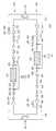
도 2는 본 발명의 일 실시예에 따른 통신용 복합 모듈 필터 장치를 나타내는 회로도이다.
도 3은 본 발명의 일 실시예에 따른 통신용 복합 모듈 필터 장치를 포함하는 소출력 중계기 시스템을 나타내는 도면이다.
도 4는 본 발명의 일 실시예에 따른 통신용 복합 모듈 필터 장치의 삽입 손실을 나타내는 그래프이다.
도 5a 및 5b는 본 발명의 일 실시예에 따른 통신용 복합 모듈 필터 장치의 밴드 폭이 3dB 및 40dB 일 경우의 삽입 손실을 나타내는 그래프이다.1 is a block diagram showing a configuration of a repeater system common in a communication system.
2 is a circuit diagram showing a communication module for a communication module according to an embodiment of the present invention.
FIG. 3 is a diagram illustrating a small power repeater system including a communication complex module filter apparatus according to an embodiment of the present invention.
4 is a graph illustrating insertion loss of a communication module filter device according to an embodiment of the present invention.
FIGS. 5A and 5B are graphs showing insertion loss when the bandwidth of a communication complex module filter apparatus according to an embodiment of the present invention is 3 dB and 40 dB, respectively.
본 명세서에서 사용되는 용어에 대해 간략히 설명하고, 본 발명에 대해 구체적으로 설명하기로 한다.The terms used in this specification will be briefly described and the present invention will be described in detail.
본 발명에서 사용되는 용어는 본 발명에서의 기능을 고려하면서 가능한 현재 널리 사용되는 일반적인 용어들을 선택하였으나, 이는 당 분야에 종사하는 기술자의 의도 또는 판례, 새로운 기술의 출현 등에 따라 달라질 수 있다. 또한, 특정한 경우는 출원인이 임의로 선정한 용어도 있으며, 이 경우 해당되는 발명의 설명 부분에서 상세히 그 의미를 기재할 것이다. 따라서 본 발명에서 사용되는 용어는 단순한 용어의 명칭이 아닌, 그 용어가 가지는 의미와 본 발명의 전반에 걸친 내용을 토대로 정의되어야 한다.While the present invention has been described in connection with what is presently considered to be the most practical and preferred embodiment, it is to be understood that the invention is not limited to the disclosed embodiments. Also, in certain cases, there may be a term selected arbitrarily by the applicant, in which case the meaning thereof will be described in detail in the description of the corresponding invention. Therefore, the term used in the present invention should be defined based on the meaning of the term, not on the name of a simple term, but on the entire contents of the present invention.
명세서 전체에서 어떤 부분이 어떤 구성요소를 "포함"한다고 할 때, 이는 특별히 반대되는 기재가 없는 한 다른 구성요소를 제외하는 것이 아니라 다른 구성요소를 더 포함할 수 있음을 의미한다. 또한, 명세서에 기재된 "...부", "모듈" 등의 용어는 적어도 하나의 기능이나 동작을 처리하는 단위를 의미하며, 이는 하드웨어 또는 소프트웨어로 구현되거나 하드웨어와 소프트웨어의 결합으로 구현될 수 있다.When an element is referred to as "including" an element throughout the specification, it is to be understood that the element may include other elements as well, without departing from the spirit or scope of the present invention. Also, the terms "part," " module, "and the like described in the specification mean units for processing at least one function or operation, which may be implemented in hardware or software or a combination of hardware and software .
아래에서는 첨부한 도면을 참고하여 본 발명의 실시예에 대하여 본 발명이 속하는 기술 분야에서 통상의 지식을 가진 자가 용이하게 실시할 수 있도록 상세히 설명한다. 그러나 본 발명은 여러 가지 상이한 형태로 구현될 수 있으며 여기에서 설명하는 실시예에 한정되지 않는다. 그리고 도면에서 본 발명을 명확하게 설명하기 위해서 설명과 관계없는 부분은 생략하였으며, 명세서 전체를 통하여 유사한 부분에 대해서는 유사한 도면 부호를 붙였다.Hereinafter, embodiments of the present invention will be described in detail with reference to the accompanying drawings so that those skilled in the art can easily carry out the present invention. The present invention may, however, be embodied in many different forms and should not be construed as limited to the embodiments set forth herein. In order to clearly illustrate the present invention, parts not related to the description are omitted, and similar parts are denoted by like reference characters throughout the specification.
도 2는 본 발명의 일 실시예에 따른 통신용 복합 모듈 필터 장치를 나타내는 회로도이고, 도 3은 본 발명의 일 실시예에 따른 통신용 복합 모듈 필터 장치를 포함하는 소출력 중계기 시스템을 나타내는 도면이며, 도 4는 본 발명의 일 실시예에 따른 통신용 복합 모듈 필터 장치의 삽입 손실을 나타내는 그래프이고, 도 5a 및 5b는 본 발명의 일 실시예에 따른 통신용 복합 모듈 필터 장치의 밴드 폭이 3dB 및 40dB 일 경우의 삽입 손실을 나타내는 그래프이다.FIG. 2 is a circuit diagram showing a communication complex module filter apparatus according to an embodiment of the present invention, FIG. 3 is a diagram illustrating a small-power repeater system including a communication complex module filter apparatus according to an embodiment of the present invention, FIGS. 5A and 5B are graphs showing insertion loss of the communication complex filter according to the embodiment of the present invention. FIGS. 5A and 5B are graphs showing the insertion loss of the communication complex filter according to an embodiment of the present invention. Is a graph showing insertion loss.
도 2를 참조하면, 본 발명의 일 실시예에 따른 통신용 복합 모듈 필터 장치(300)는 RF 신호 중 일정 주파수 대역의 신호만을 선택적으로 통과시키는 주파수 필터(310)와, 주파수 필터(310)에 의하여 통과된 일정 주파수 대역의 신호를 증폭하는 신호 증폭부(320)를 포함한다. 본 통신용 복합 필터 모듈(300)은 단일 필터 모듈에 주파수 필터(310)와 신호 증폭부(320)가 소형화되어 하나의 부품으로 구성될 수 있다.2, the communication
또한, 상기 주파수 필터(310)와 신호 증폭부(320)의 각각을 중심으로 양측에는 임피던스 정합을 위한 제1 정합부 내지 제4 정합부(311, 312, 321, 322)가 구성된다. 또한, 상기 신호 증폭부(320)의 일측에는 전원을 공급하는 전원 공급부(330)가 구비되고, 신호 증폭부(320)와 전원 공급부(330) 사이에는 임피던스 정합을 위한 제5 정합부(331)가 구비된다.The first to fourth matching
이러한 구성을 통하여 본 통신용 복합 모듈 필터 장치(300)는 주파수 필터(310)가 기능적으로 주파수 필터링을 수행시 발생되는 삽입 손실을 신호 증폭부(320)를 통하여 보상할 수 있게 된다. 이러한 기능을 구현하기 위하여, 전원과 소자 또는 2개의 소자를 접속할 경우, 반사 손실이 없도록 양자의 임피던스를 같게 하여 효율적인 전력을 전달하는 임피던스 정합 회로(Impedance matching circuit)가 구성되어 있다.With this configuration, the
상기 주파수 필터(310)는 입력되는 RF 신호 중 일정 주파수 대역의 신호만을 선택적으로 통과시키는 소자로서, 대역 통과 필터(BPF; Band Pass Filter) 또는 SAW 필터일 수 있다. 이때, 상기 주파수 필터(310)는 중심 주파수가 70MHz이고, 통과 대역은 20MHz일 수 있다. 그러나, 본 발명에서의 주파수 필터(310)의 중심 주파수와 통과 대역은 본 통신용 복합 모듈 필터 장치(300)의 용도 및 목적에 따라 다양한 주파수와 대역으로 변경될 수도 있다.The
이러한 주파수 필터(310)는, 상대적으로 좁은 주파수 대역의 신호만을 선택적으로 통과시키는 특성을 갖고 있다. 즉, 상기 주파수 필터(310)는 듀플렉서(도 3의 410)의 수신단으로 입력되는 특정 주파수 대역의 RF 신호를 특정 주파수 대역의 신호만이 필터를 통과하도록 해준다.The
상기 제1 정합부(311) 및 제2 정합부(312)는 각각 주파수 필터(310)의 입출력단 측에 구비되어 각각 입출력단측에 연결되는 소자들과의 임피던스 정합을 수행한다.The first matching
상기 제1 정합부(311)는 주파수 필터(310)의 입력단에 연결되는 제1 인덕터(L1)와, 제1 인덕터(L1)의 전후단에 병렬로 연결되는 제1 커패시터(C1) 및 제2 커패시터(C2)를 포함한다.The
상기 제2 정합부(312)는 주파수 필터(310)의 출력단에 연결되는 제2 인덕터(L2)와, 제2 인덕터(L2)의 전후단에 병렬로 연결되는 제3 커패시터(C3) 및 제4 커패시터(C4)를 포함한다.The
상기 신호 증폭부(320)는 주파수 필터(310)에 의하여 통과된 일정 주파수 대역의 신호를 증폭하는 소자로서, RF 증폭기 등이 사용될 수 있다. 이러한 신호 증폭부(320)는 17dB 내지 30dB의 증폭 용량을 가지는 증폭기(amplifier)가 사용되는 것이 바람직하다. 그러나, 본 발명에서는 신호 증폭부(320)의 증폭 용량을 한정하는 것은 아니고, 신호 증폭부(320)의 증폭 용량은 회로의 손실 부분에 대하여 어떠한 증폭 용량을 가지는 증폭기를 사용하는지 여부와 이러한 증폭기가 설치되는 개수에 따라 변경될 수도 있다. 예를 들면, 상기 신호 증폭부(320)는 증폭기 하나만으로 구성될 경우에는 1dB 내지 30dB 정도의 증폭 용량을 가질 수 있고, 필터의 전후단에 한 개씩 두 개로 구성되는 경우에는 50dB 내지 60dB의 증폭 용량을 가질 수 있다.The
상기 제3 정합부(321) 및 제4 정합부(322)는 각각 신호 증폭부(320)의 입출력단측에 구비되어 각각 입출력단측에 연결되는 소자들과의 임피던스 정합을 수행한다.The third matching
상기 제3 정합부(321)는 제2 정합부(312)에 구비된 제2 인덕터(L2)와 제4 커패시터(C4)의 접속 노드와, 신호 증폭부(320)의 입력단 사이에 연결된 제5 커패시터(C5)를 포함한다. 이때, 상기 제5 커패시터(C5)는 주파수 필터(310)의 중심 주파수(Center Frequency)에 따라서 그 용량값이 변동될 수 있다. 즉, 상기 제5 커패시터(C5)는 주파수 필터(310)의 중심 주파수인 70MHz에 매칭되는 용량을 가질 수 있다. 이를 통하여 주파수 필터(310)의 이득을 적정하게 구현되도록 할 수 있고, 후술하는 측정 항목에서 최종 손실 항목과 최종 출력단의 정재파비가 주어진 설계 범위 이내에서 작동되도록 할 수 있다.The third matching
상기 제4 정합부(322)는 신호 증폭부(320)의 출력단에 연결되는 제6 커패시터(C6)와, 신호 증폭부(320)의 출력단과 제6 커패시터(C6) 사이에 그 일단이 연결되는 제3 인덕터(L3)를 포함한다.The
또한, 상기 전원 공급부(330)는 신호 증폭부(320)에 구동전압을 공급하는 전원 공급 소자로서, +6.0V의 구동 전압을 신호 증폭부(320)에 공급할 수 있다.The
상기 제5 정합부(331)는 신호 증폭부(320)와 전원 공급부(330) 사이에 구비되어 신호 증폭부(320)와 전원 공급부(330) 사이의 임피던스 정합을 구현한다.The
상기 제5 정합부(331)는 제3 정합부(321)의 제3 인덕터(L3)의 일단의 반대인 타단에 각각 병렬로 연결되는 제7 커패시터 내지 제9 커패시터(C7, C8, C9)와, 제7 커패시터 내지 제9 커패시터(C7, C8, C9)와 전원 공급부(330) 사이에 구비되되, 각각 병렬로 연결되는 제1 저항 내지 제2 저항(R1, R2)을 포함한다.The
상기와 같이 구성된 본 통신용 복합 모듈 필터 장치는 기존의 SAW 필터가 갖는 삽입 손실 부분을 보상하는 회로를 집적화하여 SAW 필터 칩(Filter Chip)과 함께 내장함으로써, 통신 시스템을 소형 및 경량화하여 친환경 중계기에 적합하게 사용하도록 할 수 있다.The present composite multi-module filter apparatus configured as described above can integrate a circuit for compensating an insertion loss part of a conventional SAW filter and incorporate it together with a SAW filter chip (Filter Chip), thereby making the communication system compact and lightweight and suitable for environmentally friendly repeaters You can use it.
도 3을 참조하면, 본 발명의 일 실시예에 따른 통신용 복합 모듈 필터 장치(300)를 포함하는 소출력 중계기 시스템(400)은 종래의 중계기 시스템의 중간 검파단에 구비되는 IF SAW 필터가 제거된 자리에 대체되어, 시스템에서 발생되는 필터의 삽입 손실을 제거할 수 있다.3, the small
즉, 본 통신용 복합 모듈 필터 장치(300)는 주파수 필터(310)와 신호 증폭부(320)의 결합만으로 필터가 가지는 이득 손실을 보상할 수 있게 된다.That is, the present communication
도 3에 도시된 소출력 중계기 시스템(400)은 기지국으로부터 수신되는 RF 신호를 수신하여 혼합, 검출 및 증폭 처리하여 가입자의 이동통신기기(미도시)로 송신시키는 순방향 회로(401)와, 이와 반대로 이동통신기기에서 수신되는 RF 신호를 혼합, 검출 및 증폭 처리하여 기지국(미도시)으로 송신시키는 역방향 회로(402)로 구성된다.The small
이러한 중계기 시스템(400)의 순방향 회로(401)에서 기지국에서 발신되는 RF 신호가 안테나를 통해 수신되면, 수신된 신호는 저잡음 증폭기(LNA: Low Noise Amplifier, 415), 제1 RF 증폭기(420), 제1 커플러(425), 제1 대역 통과 필터(430)를 거쳐, 전달받은 신호에서 불필요한 잡음을 최대한 억압시키는 동시에 증폭시킨다. 그런 다음, 제1 혼합기(435)와 저주파수 대역 통과 필터(440)를 통하여 특정 대역의 신호를 본 통신용 복합 모듈 필터(300)로 제공한다. 본 통신용 복합 모듈 필터(330)를 통과한 신호는 제2 혼합기(450), 제2 대역 통과 필터(455), 제2 RF 증폭기(460), ATT(Attenuator, 465), 제3 RF 증폭기(470), 제3 대역 통과 필터(475), 제4 RF 증폭기(480), HPA(High Power Amplifier, 485), 제2 커플러(490)를 통과한 신호가 듀플렉서(Duplexer, 411)를 거쳐 안테나를 통하여 이동통신기기로 송신된다. 이때, 상기 위상 고정 루프(Phase Loop Lock, 445)를 통하여 주파수 간의 위상차 없이 전단에서 증폭된 신호가 다시 제1 혼합기(435)와 제2 혼합기(450)로 제공된다. 또한, 상기 순방향 회로(401)에 입력되는 신호의 상태를 검출하고자 하는 경우, 제1 커플러(425)를 통하여 특정 신호의 일부를 추출하고, 상기 추출된 신호를 제4 대역 통과 필터(426)로 해당 주파수 대역의 신호만을 통과시켜 검사기(560)를 통하여 주파수 특성을 확인할 수 있다.In the
이와 반대로, 역방향 회로는 이동통신기기에서 출력되는 신호를 듀플렉서(411)를 통하여 수신하고, 수신된 신호를 저잡음 증폭기(515), RF 증폭기(520, 555, 565, 575), 혼합기(530, 545), 저주파수 대역 필터(535), ATT(560), HPA(580), 커플러(585) 등의 다양한 소자들과 본 통신용 복합 모듈 필터(300)를 통하여 혼합, 검출 및 증폭 처리하여 듀플렉서(410)를 통하여 기지국으로 송신한다.
The reverse circuit receives the signal output from the mobile communication device through the
이하에서는 본 통신용 복합 모듈 필터 장치의 특성 실험을 수행한 결과를 도 4 내지 도 5b를 참조하여 설명하기로 한다.Hereinafter, the characteristics test of the communication module device will be described with reference to FIGS. 4 through 5B.
본 실험에 사용되는 주파수 필터는 SAW 필터로서, 공칭 주파수가 70MHz이고, 통과대역이 70±10MHz이며, 동작전압이 DC 5.0±0.1V이고, 시험대상 SAW 필터의 개수는 5개이다.The frequency filter used in this experiment is a SAW filter having a nominal frequency of 70 MHz, a passband of 70 ± 10 MHz, an operating voltage of DC 5.0 ± 0.1 V, and a number of SAW filters to be tested.
또한, 본 시험을 위한 표준 대기 조건은 온도가 15℃~ 35℃이고, 상대 습도는 25 % R.H. ~ 75 % R.H.이며, 대기압은 86㎪~ 106㎪이다.In addition, the standard atmospheric conditions for this test are temperature 15 ° C to 35 ° C and relative humidity 25% R.H. ~ 75% R.H., and the atmospheric pressure is 86 ~ 106..
본 시험에서 측정되는 항목인 삽입손실은 공칭주파수에서 손실을 의미하고, 통과대역 리플은 통과대역에서의 리플을 의미하며, 중간주파수는 공칭주파수에서 3dB 감쇄되는 주파수 밴드의 중간주파수를 의미하고, 밴드 폭(3dB, 40dB)은 공칭주파수에서 3dB 및 40dB 손실이 되는 밴드의 폭을 의미하며, Rejection은 저지대역에서의 최소 손실을 의미하고, 정재파비(SWR)는 S11 및 S22의 정재파비를 의미하며, Group Delay는 공칭주파수에서의 Group Delay를 의미하고, Group Delay Variation은 통과대역에서의 Group Delay의 최대와 최소와의 차이를 의미한다.The insertion loss measured in this test means loss at the nominal frequency, the passband ripple means the ripple in the passband, the intermediate frequency means the intermediate frequency of the frequency band which is 3dB attenuated at the nominal frequency, The width (3dB, 40dB) means the width of the band with a loss of 3dB and 40dB at the nominal frequency, rejection means the minimum loss in the stopband, and the standing wave ratio (SWR) means the standing wave ratio of S11 and S22 , Group Delay means Group Delay at nominal frequency, and Group Delay Variation means difference between maximum and minimum of Group Delay in pass band.
상기와 같은 조건을 기초로 본 시험을 수행한 결과, 다음 표 1과 같은 시험 결과를 얻게 되었다.As a result of carrying out this test on the basis of the above conditions, the test results shown in Table 1 were obtained.
[표 1][Table 1]

즉, 도 4 내지 도 5b에 도시된 바와 같이, 상기 조건 상에서 SAW 필터의 손실을 0dB까지 보상시킬 수 있음을 알 수 있다.That is, as shown in FIGS. 4 to 5B, it can be seen that the loss of the SAW filter can be compensated up to 0 dB under the above conditions.
따라서, 본 발명의 일 실시예에 따른 통신용 복합 모듈 필터 장치에 따르면, 웨이퍼 상태의 칩과 손실 보상 회로 및 임피던스 정합 회로를 상호 연계하여 SAW 필터의 주파수 필터링 시에도 입력 대비 출력 손실을 0dB까지 보상할 수 있게 된다. 이에 따라, 사용자가 통신 시스템의 설계 및 제조에 용이하도록 기존 SAW 필터가 갖는 삽입 손실 부분을 보상하는 회로를 SAW 필터 칩과 함께 내장하여 집적화함으로써, 제조 원가 절감에 기여할 수 있고 소형 경량화를 구현할 수 있다. 이와 같이 주파수 필터의 기능에 손실 보상 및 임피던스 정합을 기하는 기술에 집적화하여 모듈화하는 기술은 중계기 시스템 외에도 경량 소형화를 기하는 타 통신시스템에서도 요구되어지는 기술로써 다양한 방면에서 활용될 수 있다.
Therefore, according to the multi-module filter for communication according to the embodiment of the present invention, the chip in the wafer state, the loss compensation circuit, and the impedance matching circuit are interconnected to compensate the input-to- . Accordingly, a circuit for compensating the insertion loss of the conventional SAW filter is built in and integrated with the SAW filter chip so that the user can easily design and manufacture the communication system, thereby contributing to the reduction of the manufacturing cost and realization of the reduction in size and weight . In this way, the technology of integrating and modularizing the technology to the function of loss compensation and impedance matching to the function of the frequency filter can be utilized in various aspects as a technology required in other communication systems for lightweight and miniaturization in addition to the repeater system.
이상에서 설명한 것은 본 발명에 의한 통신용 복합 모듈 필터 장치를 실시하기 위한 하나의 실시예에 불과한 것으로서, 본 발명은 상기 실시예에 한정되지 않고, 이하의 특허청구범위에서 청구하는 바와 같이 본 발명의 요지를 벗어남이 없이 당해 발명이 속하는 분야에서 통상의 지식을 가진 자라면 누구든지 다양한 변경 실시가 가능한 범위까지 본 발명의 기술적 정신이 있다고 할 것이다.
As described above, the present invention is not limited to the above-described embodiment, but may be applied to a communication module for a communication module according to the present invention. It will be understood by those of ordinary skill in the art that various changes in form and details may be made therein without departing from the spirit and scope of the invention.
300: 통신용 복합 모듈 필터 장치310: 주파수 필터
311: 제1 정합부312: 제2 정합부
320: 신호 증폭부321: 제3 정합부
322: 제4 정합부330: 전원 공급부
331: 제5 정합부400: 소출력 중계기 시스템300: Composite module filter device for communication 310: Frequency filter
311: first matching portion 312: second matching portion
320: signal amplifying unit 321: third matching unit
322: fourth matching part 330: power supply part
331: Fifth matching section 400: Small output repeater system
Claims (7)
Translated fromKorean상기 신호 증폭부는 상기 주파수 필터의 자체 이득 손실을 보상하며,
상기 주파수 필터의 입출력단에 각각 개재되어 상기 주파수 필터와 입출력단측에 연결된 소자 간의 임피던스 정합을 구현하는 제1 정합부 및 제2 정합부; 및 상기 신호 증폭부의 입출력단에 각각 개재되어 상기 신호증폭부와 입출력단측에 연결된 소자 간의 임피던스 정합을 구현하는 제3 정합부 및 제4 정합부를 더 포함하되,
상기 제1 정합부는 상기 주파수 필터의 입력단에 연결되는 제1 인덕터; 및 상기 제1 인덕터의 전후단에 병렬로 연결되는 제1 커패시터 및 제2 커패시터를 포함하고, 상기 제2 정합부는 상기 주파수 필터의 출력단에 연결되는 제2 인덕터; 및 상기 제2 인덕터의 전후단에 병렬로 연결되는 제3 커패시터 및 제4 커패시터를 포함하며, 상기 제3 정합부는 상기 제2 인덕터와 상기 제4 커패시터의 접속 노드와 상기 신호 증폭부의 입력단 사이에 연결된 제5 커패시터를 포함하고, 상기 제4 정합부는 상기 신호 증폭부의 출력단에 연결되는 제 6 커패시터 및 상기 신호 증폭부의 출력단과 상기 제6 커패시터 사이에 그 일단이 연결되는 제3 인덕터를 포함하고,
상기 신호 증폭부에 전원을 공급하는 전원 공급부를 더 포함하되,
상기 전원 공급부와 신호 증폭부 사이에는 소자간의 임피던스 정합을 구현하는 제5 정합부를 포함하고,
상기 제5 정합부는 상기 제3 인덕터의 일단의 반대인 타단에 각각 병렬로 연결되는 제7 커패시터 내지 제9 커패시터 및 상기 제7 커패시터 내지 제9 커패시터와 상기 전원 공급부 사이에 구비되되, 각각 병렬로 연결되는 제1 저항 내지 제2 저항을 포함하는 것을 특징으로 하는 통신용 복합 모듈 필터 장치.
A frequency filter for selectively passing only a signal of a predetermined frequency band among the RF signals; And a signal amplifier for amplifying the signal of the certain frequency band passed,
The signal amplifying unit compensates for the self-gain loss of the frequency filter,
A first matching unit and a second matching unit which are respectively disposed at the input and output ends of the frequency filter to implement impedance matching between the frequency filter and the elements connected to the input and output ends; And a third matching unit and a fourth matching unit which are respectively disposed at the input and output ends of the signal amplifying unit to implement the impedance matching between the signal amplifying unit and the elements connected to the input / output end,
Wherein the first matching unit includes: a first inductor connected to an input terminal of the frequency filter; And a first capacitor and a second capacitor connected in parallel to the front and rear ends of the first inductor, wherein the second matching unit includes: a second inductor connected to an output terminal of the frequency filter; And a third capacitor and a fourth capacitor connected in parallel at the front and rear ends of the second inductor, and the third matching unit is connected between the connection node of the second inductor and the fourth capacitor and the input terminal of the signal amplification unit And a fourth inductor whose one end is connected between the output terminal of the signal amplification unit and the sixth capacitor, and the fourth inductor is connected between the output terminal of the signal amplification unit and the sixth capacitor,
And a power supply unit for supplying power to the signal amplification unit,
And a fifth matching unit between the power supply unit and the signal amplifying unit to implement impedance matching between the devices,
The fifth matching unit includes a seventh capacitor to a ninth capacitor connected in parallel to the other end of the third inductor opposite to the one end of the third inductor, and a seventh capacitor connected between the seventh capacitor through the ninth capacitor and the power supply unit, And a second resistor connected between the first resistor and the second resistor.
상기 주파수 필터는 대역 통과 필터 또는 SAW 필터인 것을 특징으로 하는 통신용 복합 모듈 필터 장치.
The method according to claim 1,
Wherein the frequency filter is a band-pass filter or a SAW filter.
상기 주파수 필터는 중심 주파수가 70MHz이고, 통과 대역은 20MHz인 것을 특징으로 하는 통신용 복합 모듈 필터 장치.
The method according to claim 1,
Wherein the frequency filter has a center frequency of 70 MHz and a pass band of 20 MHz.
상기 신호 증폭부는 17dB 내지 30dB의 증폭 용량을 가지는 것을 특징으로 하는 통신용 복합 모듈 필터 장치.The method according to claim 1,
Wherein the signal amplification unit has an amplification capacity of 17 dB to 30 dB.
Priority Applications (1)
| Application Number | Priority Date | Filing Date | Title |
|---|---|---|---|
| KR1020140139355AKR101522332B1 (en) | 2014-10-15 | 2014-10-15 | Compound module filter device for communication |
Applications Claiming Priority (1)
| Application Number | Priority Date | Filing Date | Title |
|---|---|---|---|
| KR1020140139355AKR101522332B1 (en) | 2014-10-15 | 2014-10-15 | Compound module filter device for communication |
Publications (1)
| Publication Number | Publication Date |
|---|---|
| KR101522332B1true KR101522332B1 (en) | 2015-05-26 |
Family
ID=53395290
Family Applications (1)
| Application Number | Title | Priority Date | Filing Date |
|---|---|---|---|
| KR1020140139355AActiveKR101522332B1 (en) | 2014-10-15 | 2014-10-15 | Compound module filter device for communication |
Country Status (1)
| Country | Link |
|---|---|
| KR (1) | KR101522332B1 (en) |
Citations (2)
| Publication number | Priority date | Publication date | Assignee | Title |
|---|---|---|---|---|
| KR0138077B1 (en)* | 1990-10-15 | 1998-06-15 | 하비 피. 화이트 | Linear gain control amplifier |
| JP2005101893A (en)* | 2003-09-25 | 2005-04-14 | Ube Ind Ltd | Power amplifier module |
- 2014
- 2014-10-15KRKR1020140139355Apatent/KR101522332B1/enactiveActive
Patent Citations (2)
| Publication number | Priority date | Publication date | Assignee | Title |
|---|---|---|---|---|
| KR0138077B1 (en)* | 1990-10-15 | 1998-06-15 | 하비 피. 화이트 | Linear gain control amplifier |
| JP2005101893A (en)* | 2003-09-25 | 2005-04-14 | Ube Ind Ltd | Power amplifier module |
Similar Documents
| Publication | Publication Date | Title |
|---|---|---|
| US6567648B1 (en) | System combining radio frequency transmitter and receiver using circulator and method for canceling transmission signal thereof | |
| CN103503314B (en) | MEMS tunable notch filter frequency automatic control loop system and method | |
| JP6500913B2 (en) | High frequency circuit component and communication device | |
| US10128796B2 (en) | Power amplification module and front end circuit | |
| US20160211820A1 (en) | Multiband rf device | |
| US20150118978A1 (en) | Transmit and receive rf multiplexer | |
| US10340855B2 (en) | Doherty amplifier | |
| US9214908B2 (en) | Amplification circuit | |
| CN211606532U (en) | High-frequency signal transceiving circuit | |
| WO2019128974A1 (en) | Signal receiving circuit, signal processing chip, communication equipment and signal receiving method | |
| KR20180125842A (en) | Multi-band radio-frequency transmitter with receiving band variable filtering function | |
| US10069523B2 (en) | Power amplification module | |
| KR101522332B1 (en) | Compound module filter device for communication | |
| CN101826886B (en) | Transceiving device with functions of power amplification and frequency hopping | |
| JP2008154201A (en) | Transmitter | |
| JP2017163232A (en) | Filter circuit, duplexer circuit, and front-end circuit | |
| KR100884374B1 (en) | Heterogeneous intercommunication module for communication | |
| KR100423187B1 (en) | Multi-band Power amplifier | |
| KR100962252B1 (en) | Filter module suppressing interference signal | |
| JP2009060511A (en) | Communication device | |
| KR200291022Y1 (en) | Only one frequency bilateral repeating system | |
| JP2009218907A (en) | Power amplifier | |
| KR100907871B1 (en) | Transmitter-less switch that shares LAN and PA matching devices | |
| KR101441616B1 (en) | Transmission line having a variable characteristic impedance | |
| CN114531167A (en) | High-frequency signal transceiving circuit |
Legal Events
| Date | Code | Title | Description |
|---|---|---|---|
| PA0109 | Patent application | Patent event code:PA01091R01D Comment text:Patent Application Patent event date:20141015 | |
| PA0201 | Request for examination | ||
| PA0302 | Request for accelerated examination | Patent event date:20141112 Patent event code:PA03022R01D Comment text:Request for Accelerated Examination Patent event date:20141015 Patent event code:PA03021R01I Comment text:Patent Application | |
| PE0902 | Notice of grounds for rejection | Comment text:Notification of reason for refusal Patent event date:20150210 Patent event code:PE09021S01D | |
| E701 | Decision to grant or registration of patent right | ||
| PE0701 | Decision of registration | Patent event code:PE07011S01D Comment text:Decision to Grant Registration Patent event date:20150427 | |
| GRNT | Written decision to grant | ||
| PR0701 | Registration of establishment | Comment text:Registration of Establishment Patent event date:20150515 Patent event code:PR07011E01D | |
| PR1002 | Payment of registration fee | Payment date:20150518 End annual number:3 Start annual number:1 | |
| PG1601 | Publication of registration | ||
| FPAY | Annual fee payment | Payment date:20180406 Year of fee payment:4 | |
| PR1001 | Payment of annual fee | Payment date:20180406 Start annual number:4 End annual number:4 | |
| FPAY | Annual fee payment | Payment date:20190311 Year of fee payment:5 | |
| PR1001 | Payment of annual fee | Payment date:20190311 Start annual number:5 End annual number:5 | |
| FPAY | Annual fee payment | Payment date:20200305 Year of fee payment:6 | |
| PR1001 | Payment of annual fee | Payment date:20200305 Start annual number:6 End annual number:6 | |
| PR1001 | Payment of annual fee | Payment date:20210510 Start annual number:7 End annual number:7 | |
| PR1001 | Payment of annual fee | Payment date:20220503 Start annual number:8 End annual number:8 | |
| PR1001 | Payment of annual fee | Payment date:20230531 Start annual number:9 End annual number:9 |