KR101520423B1 - Touch sensor in-cell type liquid crystal display device and method of fabricating the same - Google Patents
Touch sensor in-cell type liquid crystal display device and method of fabricating the sameDownload PDFInfo
- Publication number
- KR101520423B1 KR101520423B1KR1020110037243AKR20110037243AKR101520423B1KR 101520423 B1KR101520423 B1KR 101520423B1KR 1020110037243 AKR1020110037243 AKR 1020110037243AKR 20110037243 AKR20110037243 AKR 20110037243AKR 101520423 B1KR101520423 B1KR 101520423B1
- Authority
- KR
- South Korea
- Prior art keywords
- wiring
- gate
- electrode
- contact hole
- sensing
- Prior art date
- Legal status (The legal status is an assumption and is not a legal conclusion. Google has not performed a legal analysis and makes no representation as to the accuracy of the status listed.)
- Active
Links
Images


Classifications
- G—PHYSICS
- G02—OPTICS
- G02F—OPTICAL DEVICES OR ARRANGEMENTS FOR THE CONTROL OF LIGHT BY MODIFICATION OF THE OPTICAL PROPERTIES OF THE MEDIA OF THE ELEMENTS INVOLVED THEREIN; NON-LINEAR OPTICS; FREQUENCY-CHANGING OF LIGHT; OPTICAL LOGIC ELEMENTS; OPTICAL ANALOGUE/DIGITAL CONVERTERS
- G02F1/00—Devices or arrangements for the control of the intensity, colour, phase, polarisation or direction of light arriving from an independent light source, e.g. switching, gating or modulating; Non-linear optics
- G02F1/01—Devices or arrangements for the control of the intensity, colour, phase, polarisation or direction of light arriving from an independent light source, e.g. switching, gating or modulating; Non-linear optics for the control of the intensity, phase, polarisation or colour
- G02F1/13—Devices or arrangements for the control of the intensity, colour, phase, polarisation or direction of light arriving from an independent light source, e.g. switching, gating or modulating; Non-linear optics for the control of the intensity, phase, polarisation or colour based on liquid crystals, e.g. single liquid crystal display cells
- G02F1/133—Constructional arrangements; Operation of liquid crystal cells; Circuit arrangements
- G02F1/1333—Constructional arrangements; Manufacturing methods
- G02F1/13338—Input devices, e.g. touch panels
- G—PHYSICS
- G02—OPTICS
- G02F—OPTICAL DEVICES OR ARRANGEMENTS FOR THE CONTROL OF LIGHT BY MODIFICATION OF THE OPTICAL PROPERTIES OF THE MEDIA OF THE ELEMENTS INVOLVED THEREIN; NON-LINEAR OPTICS; FREQUENCY-CHANGING OF LIGHT; OPTICAL LOGIC ELEMENTS; OPTICAL ANALOGUE/DIGITAL CONVERTERS
- G02F1/00—Devices or arrangements for the control of the intensity, colour, phase, polarisation or direction of light arriving from an independent light source, e.g. switching, gating or modulating; Non-linear optics
- G02F1/01—Devices or arrangements for the control of the intensity, colour, phase, polarisation or direction of light arriving from an independent light source, e.g. switching, gating or modulating; Non-linear optics for the control of the intensity, phase, polarisation or colour
- G02F1/13—Devices or arrangements for the control of the intensity, colour, phase, polarisation or direction of light arriving from an independent light source, e.g. switching, gating or modulating; Non-linear optics for the control of the intensity, phase, polarisation or colour based on liquid crystals, e.g. single liquid crystal display cells
- G02F1/133—Constructional arrangements; Operation of liquid crystal cells; Circuit arrangements
- G02F1/136—Liquid crystal cells structurally associated with a semi-conducting layer or substrate, e.g. cells forming part of an integrated circuit
- G02F1/1362—Active matrix addressed cells
- G02F1/136227—Through-hole connection of the pixel electrode to the active element through an insulation layer
- G—PHYSICS
- G02—OPTICS
- G02F—OPTICAL DEVICES OR ARRANGEMENTS FOR THE CONTROL OF LIGHT BY MODIFICATION OF THE OPTICAL PROPERTIES OF THE MEDIA OF THE ELEMENTS INVOLVED THEREIN; NON-LINEAR OPTICS; FREQUENCY-CHANGING OF LIGHT; OPTICAL LOGIC ELEMENTS; OPTICAL ANALOGUE/DIGITAL CONVERTERS
- G02F1/00—Devices or arrangements for the control of the intensity, colour, phase, polarisation or direction of light arriving from an independent light source, e.g. switching, gating or modulating; Non-linear optics
- G02F1/01—Devices or arrangements for the control of the intensity, colour, phase, polarisation or direction of light arriving from an independent light source, e.g. switching, gating or modulating; Non-linear optics for the control of the intensity, phase, polarisation or colour
- G02F1/13—Devices or arrangements for the control of the intensity, colour, phase, polarisation or direction of light arriving from an independent light source, e.g. switching, gating or modulating; Non-linear optics for the control of the intensity, phase, polarisation or colour based on liquid crystals, e.g. single liquid crystal display cells
- G02F1/133—Constructional arrangements; Operation of liquid crystal cells; Circuit arrangements
- G02F1/136—Liquid crystal cells structurally associated with a semi-conducting layer or substrate, e.g. cells forming part of an integrated circuit
- G02F1/1362—Active matrix addressed cells
- G02F1/136286—Wiring, e.g. gate line, drain line
- G—PHYSICS
- G02—OPTICS
- G02F—OPTICAL DEVICES OR ARRANGEMENTS FOR THE CONTROL OF LIGHT BY MODIFICATION OF THE OPTICAL PROPERTIES OF THE MEDIA OF THE ELEMENTS INVOLVED THEREIN; NON-LINEAR OPTICS; FREQUENCY-CHANGING OF LIGHT; OPTICAL LOGIC ELEMENTS; OPTICAL ANALOGUE/DIGITAL CONVERTERS
- G02F1/00—Devices or arrangements for the control of the intensity, colour, phase, polarisation or direction of light arriving from an independent light source, e.g. switching, gating or modulating; Non-linear optics
- G02F1/01—Devices or arrangements for the control of the intensity, colour, phase, polarisation or direction of light arriving from an independent light source, e.g. switching, gating or modulating; Non-linear optics for the control of the intensity, phase, polarisation or colour
- G02F1/13—Devices or arrangements for the control of the intensity, colour, phase, polarisation or direction of light arriving from an independent light source, e.g. switching, gating or modulating; Non-linear optics for the control of the intensity, phase, polarisation or colour based on liquid crystals, e.g. single liquid crystal display cells
- G02F1/133—Constructional arrangements; Operation of liquid crystal cells; Circuit arrangements
- G02F1/136—Liquid crystal cells structurally associated with a semi-conducting layer or substrate, e.g. cells forming part of an integrated circuit
- G02F1/1362—Active matrix addressed cells
- G02F1/1368—Active matrix addressed cells in which the switching element is a three-electrode device
- G—PHYSICS
- G06—COMPUTING OR CALCULATING; COUNTING
- G06F—ELECTRIC DIGITAL DATA PROCESSING
- G06F3/00—Input arrangements for transferring data to be processed into a form capable of being handled by the computer; Output arrangements for transferring data from processing unit to output unit, e.g. interface arrangements
- G06F3/01—Input arrangements or combined input and output arrangements for interaction between user and computer
- G06F3/03—Arrangements for converting the position or the displacement of a member into a coded form
- G06F3/041—Digitisers, e.g. for touch screens or touch pads, characterised by the transducing means
- G06F3/0412—Digitisers structurally integrated in a display
- G—PHYSICS
- G06—COMPUTING OR CALCULATING; COUNTING
- G06F—ELECTRIC DIGITAL DATA PROCESSING
- G06F3/00—Input arrangements for transferring data to be processed into a form capable of being handled by the computer; Output arrangements for transferring data from processing unit to output unit, e.g. interface arrangements
- G06F3/01—Input arrangements or combined input and output arrangements for interaction between user and computer
- G06F3/03—Arrangements for converting the position or the displacement of a member into a coded form
- G06F3/041—Digitisers, e.g. for touch screens or touch pads, characterised by the transducing means
- G06F3/044—Digitisers, e.g. for touch screens or touch pads, characterised by the transducing means by capacitive means
- G06F3/0443—Digitisers, e.g. for touch screens or touch pads, characterised by the transducing means by capacitive means using a single layer of sensing electrodes
- G—PHYSICS
- G06—COMPUTING OR CALCULATING; COUNTING
- G06F—ELECTRIC DIGITAL DATA PROCESSING
- G06F3/00—Input arrangements for transferring data to be processed into a form capable of being handled by the computer; Output arrangements for transferring data from processing unit to output unit, e.g. interface arrangements
- G06F3/01—Input arrangements or combined input and output arrangements for interaction between user and computer
- G06F3/03—Arrangements for converting the position or the displacement of a member into a coded form
- G06F3/041—Digitisers, e.g. for touch screens or touch pads, characterised by the transducing means
- G06F3/044—Digitisers, e.g. for touch screens or touch pads, characterised by the transducing means by capacitive means
- G06F3/0446—Digitisers, e.g. for touch screens or touch pads, characterised by the transducing means by capacitive means using a grid-like structure of electrodes in at least two directions, e.g. using row and column electrodes
- H—ELECTRICITY
- H10—SEMICONDUCTOR DEVICES; ELECTRIC SOLID-STATE DEVICES NOT OTHERWISE PROVIDED FOR
- H10D—INORGANIC ELECTRIC SEMICONDUCTOR DEVICES
- H10D86/00—Integrated devices formed in or on insulating or conducting substrates, e.g. formed in silicon-on-insulator [SOI] substrates or on stainless steel or glass substrates
- H10D86/01—Manufacture or treatment
- H10D86/021—Manufacture or treatment of multiple TFTs
- H10D86/0221—Manufacture or treatment of multiple TFTs comprising manufacture, treatment or patterning of TFT semiconductor bodies
- H10D86/0223—Manufacture or treatment of multiple TFTs comprising manufacture, treatment or patterning of TFT semiconductor bodies comprising crystallisation of amorphous, microcrystalline or polycrystalline semiconductor materials
- G—PHYSICS
- G02—OPTICS
- G02F—OPTICAL DEVICES OR ARRANGEMENTS FOR THE CONTROL OF LIGHT BY MODIFICATION OF THE OPTICAL PROPERTIES OF THE MEDIA OF THE ELEMENTS INVOLVED THEREIN; NON-LINEAR OPTICS; FREQUENCY-CHANGING OF LIGHT; OPTICAL LOGIC ELEMENTS; OPTICAL ANALOGUE/DIGITAL CONVERTERS
- G02F1/00—Devices or arrangements for the control of the intensity, colour, phase, polarisation or direction of light arriving from an independent light source, e.g. switching, gating or modulating; Non-linear optics
- G02F1/01—Devices or arrangements for the control of the intensity, colour, phase, polarisation or direction of light arriving from an independent light source, e.g. switching, gating or modulating; Non-linear optics for the control of the intensity, phase, polarisation or colour
- G02F1/13—Devices or arrangements for the control of the intensity, colour, phase, polarisation or direction of light arriving from an independent light source, e.g. switching, gating or modulating; Non-linear optics for the control of the intensity, phase, polarisation or colour based on liquid crystals, e.g. single liquid crystal display cells
- G02F1/133—Constructional arrangements; Operation of liquid crystal cells; Circuit arrangements
- G02F1/1333—Constructional arrangements; Manufacturing methods
- G02F1/1343—Electrodes
- G02F1/134309—Electrodes characterised by their geometrical arrangement
- G02F1/134372—Electrodes characterised by their geometrical arrangement for fringe field switching [FFS] where the common electrode is not patterned
- G—PHYSICS
- G02—OPTICS
- G02F—OPTICAL DEVICES OR ARRANGEMENTS FOR THE CONTROL OF LIGHT BY MODIFICATION OF THE OPTICAL PROPERTIES OF THE MEDIA OF THE ELEMENTS INVOLVED THEREIN; NON-LINEAR OPTICS; FREQUENCY-CHANGING OF LIGHT; OPTICAL LOGIC ELEMENTS; OPTICAL ANALOGUE/DIGITAL CONVERTERS
- G02F1/00—Devices or arrangements for the control of the intensity, colour, phase, polarisation or direction of light arriving from an independent light source, e.g. switching, gating or modulating; Non-linear optics
- G02F1/01—Devices or arrangements for the control of the intensity, colour, phase, polarisation or direction of light arriving from an independent light source, e.g. switching, gating or modulating; Non-linear optics for the control of the intensity, phase, polarisation or colour
- G02F1/13—Devices or arrangements for the control of the intensity, colour, phase, polarisation or direction of light arriving from an independent light source, e.g. switching, gating or modulating; Non-linear optics for the control of the intensity, phase, polarisation or colour based on liquid crystals, e.g. single liquid crystal display cells
- G02F1/133—Constructional arrangements; Operation of liquid crystal cells; Circuit arrangements
- G02F1/136—Liquid crystal cells structurally associated with a semi-conducting layer or substrate, e.g. cells forming part of an integrated circuit
- G02F1/1362—Active matrix addressed cells
- G02F1/136286—Wiring, e.g. gate line, drain line
- G02F1/136295—Materials; Compositions; Manufacture processes
- G—PHYSICS
- G06—COMPUTING OR CALCULATING; COUNTING
- G06F—ELECTRIC DIGITAL DATA PROCESSING
- G06F2203/00—Indexing scheme relating to G06F3/00 - G06F3/048
- G06F2203/041—Indexing scheme relating to G06F3/041 - G06F3/045
- G06F2203/04103—Manufacturing, i.e. details related to manufacturing processes specially suited for touch sensitive devices
- G—PHYSICS
- G06—COMPUTING OR CALCULATING; COUNTING
- G06F—ELECTRIC DIGITAL DATA PROCESSING
- G06F3/00—Input arrangements for transferring data to be processed into a form capable of being handled by the computer; Output arrangements for transferring data from processing unit to output unit, e.g. interface arrangements
- G06F3/01—Input arrangements or combined input and output arrangements for interaction between user and computer
- G06F3/03—Arrangements for converting the position or the displacement of a member into a coded form
- G06F3/041—Digitisers, e.g. for touch screens or touch pads, characterised by the transducing means
- G06F3/047—Digitisers, e.g. for touch screens or touch pads, characterised by the transducing means using sets of wires, e.g. crossed wires
Landscapes
- Physics & Mathematics (AREA)
- Engineering & Computer Science (AREA)
- Nonlinear Science (AREA)
- General Physics & Mathematics (AREA)
- General Engineering & Computer Science (AREA)
- Theoretical Computer Science (AREA)
- Crystallography & Structural Chemistry (AREA)
- Chemical & Material Sciences (AREA)
- Mathematical Physics (AREA)
- Optics & Photonics (AREA)
- Human Computer Interaction (AREA)
- Microelectronics & Electronic Packaging (AREA)
- Liquid Crystal (AREA)
- Devices For Indicating Variable Information By Combining Individual Elements (AREA)
Abstract
Translated fromKoreanDescription
Translated fromKorean본 발명은 액정표시장치에 관한 것이며, 특히 콘택홀 내부에서 금속패턴간 접촉 불량을 방지할 수 있는 터치센서 인셀 타입 액정표시장치용 어레이 기판 및 이의 제조방법에 관한 것이다.
BACKGROUND OF THE INVENTION 1. Field of the Invention The present invention relates to a liquid crystal display device, and more particularly, to an array substrate for an in-cell type liquid crystal display device capable of preventing contact failure between metal patterns in a contact hole and a method of manufacturing the same.
최근에 액정표시장치는 소비전력이 낮고, 휴대성이 양호한 기술 집약적이며, 부가가치가 높은 차세대 첨단 디스플레이(display)소자로 각광받고 있다.Recently, liquid crystal display devices have been attracting attention as next generation advanced display devices with low power consumption, good portability, and high value-added.
이러한 액정표시장치 중에서도 각 화소(pixel)별로 전압의 온(on),오프(off)를 조절할 수 있는 스위칭 소자인 박막트랜지스터가 구비된 액티브 매트릭스형 액정표시장치가 해상도 및 동영상 구현능력이 뛰어나 가장 주목받고 있다.Of these liquid crystal display devices, an active matrix type liquid crystal display device having a thin film transistor, which is a switching device capable of controlling voltage on and off for each pixel, .
일반적으로, 액정표시장치는 박막트랜지스터 및 화소전극을 형성하는 어레이 기판 제조 공정과 컬러필터 및 공통 전극을 형성하는 컬러필터 기판 제조 공정을 통해 각각 어레이 기판 및 컬러필터 기판을 형성하고, 이들 두 기판 사이에 액정을 개재하는 셀 공정을 거쳐 완성된다.In general, a liquid crystal display device forms an array substrate and a color filter substrate through an array substrate manufacturing process for forming thin film transistors and pixel electrodes, and a color filter substrate manufacturing process for forming color filters and common electrodes, And a liquid crystal interposed therebetween.
좀 더 자세히, 일반적인 액정표시장치의 분해사시도인 도 1을 참조하여 설명하면, 액정층(30)을 사이에 두고 어레이 기판(10)과 컬러필터 기판(20)이 대면 합착된 구성을 갖는데, 이중 하부의 어레이 기판(10)은 투명한 기판(12)의 상면으로 종횡 교차 배열되어 다수의 화소영역(P)을 정의하는 복수개의 게이트 배선(14)과 데이터 배선(16)을 포함하며, 이들 두 배선(14, 16)의 교차지점에는 박막트랜지스터(Tr)가 구비되어 각 화소영역(P)에 마련된 화소전극(18)과 일대일 대응 접속되어 있다.1, which is an exploded perspective view of a general liquid crystal display device, the
또한, 상기 어레이 기판(10)과 마주보는 상부의 컬러필터 기판(20)은 투명기판(22)의 배면으로 상기 게이트 배선(14)과 데이터 배선(16) 그리고 박막트랜지스터(Tr) 등의 비표시영역을 가리도록 각 화소영역(P)을 둘러싸는 격자 형상의 블랙매트릭스(25)가 형성되어 있으며, 이들 격자 내부에서 각 화소영역(P)에 대응되게 순차적으로 반복 배열된 적(R), 녹(G), 청(B)색의 컬러필터 패턴(26a, 26b, 26c)을 포함하는 컬러필터층(26)이 형성되어 있으며, 상기 블랙매트릭스(25)와 컬러필터층(26)의 전면에 걸쳐 투명한 공통전극(28)이 구비되어 있다.The upper portion of the
그리고, 도면상에 도시되지는 않았지만, 이들 두 기판(10, 20)은 그 사이로 개재된 액정층(30)의 누설을 방지하기 위하여 가장자리 따라 실링제(sealant) 등으로 봉함된 상태에서 각 기판(10, 20)과 액정층(30)의 경계부분에는 액정의 분자배열 방향에 신뢰성을 부여하는 상, 하부 배향막이 개재되며, 각 기판(10, 20)의 적어도 하나의 외측면에는 편광판(미도시)이 구비되어 있다.Although not shown in the drawings, the two
또한, 어레이 기판(10)의 외측면으로는 백라이트(back-light)가 구비되어 빛을 공급하는 바, 게이트 배선(14)으로 박막트랜지스터(Tr)의 온(on)/오프(off) 신호가 순차적으로 스캔 인가되어 선택된 화소영역(P)의 화소전극(18)에 데이터배선(16)의 화상신호가 전달되면 공통전극(28)과 화소전극(18) 사이의 수직전계에 의해 그 사이의 액정분자가 구동되고, 이에 따른 빛의 투과율 변화로 여러 가지 화상을 표시할 수 있다.On the outer surface of the
하지만 전술한 구성을 갖는 액정표시장치는 시야각 특성이 우수하지 못하므로 근래 들어서는 동일한 어레이 기판에 공통전극과 화소전극이 배치되어 수평전계 에 의해 액정분자를 구동하는 횡전계형 또는 프린지 전계에 의해 구동되는 프린지 필드 스위칭 모드 액정표시장치가 제안되었다.However, since the liquid crystal display device having the above-described configuration is not excellent in viewing angle characteristics, a common electrode and a pixel electrode are disposed on the same array substrate in recent years, and a transverse electric field for driving liquid crystal molecules by a horizontal electric field or a fringe A field switching mode liquid crystal display device has been proposed.
그리고, 이러한 횡전계형 및 프린지 필드 스위칭 모드 액정표시장치는 TV, 프로젝터, 휴대폰, PDA 등 다양한 응용제품에 이용되고 있으며, 이러한 응용제품들은 최근에 화면을 터치하여 동작할 수 있도록 터치 기능이 기본적으로 장착되고 있는 실정이다. 이렇게 터치 기능이 구비된 액정표시장치를 통상 터치센서 인셀 타입 액정표시장치라 칭하고 있다.These transverse electric field type and fringe field switching mode liquid crystal display devices are used in various applications such as TV, projector, mobile phone, and PDA. These applications are basically equipped with a touch function in order to operate by touching the screen recently . Such a liquid crystal display device having a touch function is generally called a touch sensor in-cell type liquid crystal display device.
터치센서 인셀 타입 액정표시장치용 어레이 기판에는 터치 센싱 기능 수행을 위해 전술 바와 같은 액정표시장치의 일반적인 구성 요소 일례로 게이트 및 데이터 배선 이외에 추가적으로 사용자의 터치 시 이를 감지하는 다수의 터치 블록과 이와 연결된 센싱 배선의 구성이 더욱 필요로 되고 있다.In order to perform a touch sensing function, an array substrate for a touch sensor type in-cell type liquid crystal display includes a plurality of touch blocks for sensing a user's touch in addition to a gate and a data line, A wiring structure is further required.
따라서, 이러한 구성을 갖는 터치센서 인셀 타입 액정표시장치용 어레이 기판은 통상 우수한 이동도 특성을 갖는 폴리실리콘을 반도체층으로 하는 박막트랜지스터가 구비되는 경우 통상 11회의 마스크 공정을 진행하고 있다.Therefore, in an array substrate for an in-cell type liquid crystal display device having a touch sensor having such a structure, when a thin film transistor having a semiconductor layer of polysilicon having excellent mobility characteristics is provided, the mask process is usually performed 11 times.
이러한 터치 인셀 타입 액정표시장치용 어레이 기판에는 상기 절연층으로서 게이트 절연막, 층간절연막, 보조 절연층 및 제 1, 2 보호층이 구비되고 있는 실정이다.In such an array substrate for a touch-insensitive-type liquid crystal display device, a gate insulating film, an interlayer insulating film, an auxiliary insulating layer, and first and second protective layers are provided as the insulating layer.
이때, 이러한 절연층 중 상기 보조 절연층은 금속물질로 이루어진 구성요소 예를들면 데이터 배선과 소스 및 드레인 전극과 유기절연물질로 이루어진 제 1 보호층과의 접착력 향상을 위해 무기절연물질을 증착함으로써 형성되고 있는데, 이러한 보조 절연층은 생략함으로써 총 2개만을 형성하는 구성을 갖도록 하기 위해 노력하고 있다.At this time, among the insulating layers, the auxiliary insulating layer may be formed by depositing an inorganic insulating material to improve adhesion between a component made of a metal material, for example, a data line, a source and a drain electrode, and a first protective layer made of an organic insulating material However, efforts have been made to have a structure in which only a total of two are formed by omitting the auxiliary insulating layer.
하지만, 이렇게 무기절연물질로 이루어진 보조 절연층을 삭제하는 경우 제 2 보호층 내에 구비된 콘택홀을 통해 노출되는 드레인 전극과 데이터 배선과 연결된 데이터 패드전극은 상기 제 1 보호층 상부에 형성되는 공통전극 패터닝시 사용되는 식각액과 상기 드레인 전극 및 데이터 배선과 동일한 물질로 이루어진 센싱배선의 패터닝시 사용되는 식각액에 노출됨으로써 손상을 받게 됨으로써 최종적으로 상기 콘택홀을 통해 연결되어야 하는 구성요소와의 접촉 특성이 저하되는 접촉 불량이 다발하는 문제가 발생하고 있다.
However, when the auxiliary insulating layer made of the inorganic insulating material is removed, the drain electrode exposed through the contact hole provided in the second passivation layer and the data pad electrode connected to the data line are electrically connected to the common electrode The contact hole is damaged by being exposed to the etchant used for patterning and the etchant used for patterning the sensing wiring made of the same material as the drain electrode and the data wire so that the contact property with the component to be finally connected through the contact hole is deteriorated A problem of frequent contact defects occurs.
상기 문제점을 해결하기 위해서, 본 발명에서는 콘택홀을 통해 노출된 구성요소가 이후 단계의 구성요소 패터닝을 위한 식각액에 의해 손상을 받음으로써 발생되는 두 구성요소의 접촉 불량을 방지할 수 있는 터치센서 인셀 타입 액정표시장치용 어레이 기판을 제공하는 것을 그 목적으로 한다.
In order to solve the above problems, according to the present invention, there is provided a touch sensor in which components exposed through a contact hole are prevented from being in contact with two components caused by damage to an etchant for patterning a component in a subsequent step, Type liquid crystal display device.
상기 목적을 달성하기 위한 본 발명에 따른 터치센서 인셀 타입 액정표시장치용 어레이 기판은, 다수의 화소영역을 갖는 표시영역과 이의 외측으로 비표시영역이 정의되며 상기 표시영역 내에 다수의 화소영역을 하나의 그룹으로 하는 터치블럭이 다수개 정의된 기판 상의 각 화소영역의 경계에 제 1 절연막을 개재하여 서로 교차하며 형성된 게이트 및 데이터 배선과; 상기 각 화소영역 내에 상기 게이트 및 데이터 배선과 연결되며 형성된 박막트랜지스터와; 유기절연물질로 이루어지며, 상기 박막트랜지스터 위로 상기 박막트랜지스터의 드레인 전극을 노출시키는 제 1 드레인 콘택홀 형성된 제 1 보호층과; 상기 제 1 보호층 위로 상기 각 터치블럭 별로 이격하며 형성된 공통전극과; 상기 제 1 보호층 위로 상기 공통전극과 이격하며 상기 제 1 드레인 콘택홀과 중첩하며 상기 공통전극을 이루는 동일한 물질로 형성된 도전성 식각 방지패턴과; 상기 공통전극 위로 상기 게이트 배선과 중첩하도록 형성된 x센싱배선 및 상기 데이터 배선과 중첩하도록 형성된 y센싱배선과; 상기 공통전극과 x센싱배선 및 y센싱배선 위로 상기 기판 전면에 형성되며, 상기 도전성 식각 방지패턴을 노출시키는 제 2 드레인 콘택홀을 가지며 형성된 제 2 보호층과; 상기 제 2 보호층 위로 상기 제 2 드레인 콘택홀을 통해 상기 도전성 식각 방지패턴과 접촉하며 상기 각 화소영역 별로 형성되며, 다수의 바(bar) 형태의 개구를 갖는 화소전극을 포함하며, 상기 비표시영역에는 패드부가 정의되며, 상기 비표시영역에는 상기 게이트 배선이 형성된 동일한 층에 상기 게이트 배선과 연결된 게이트 링크배선이 형성되며, 상기 패드부에는 상기 게이트 링크배선과 연결된 게이트 패드전극이 형성되고, 상기 비표시영역에는 상기 데이터 배선이 형성된 동일한 층에 상기 데이터 배선과 연결된 데이터 링크배선이 형성되며, 상기 패드부에는 상기 데이터 링크배선과 연결된 데이터 패드전극이 형성되며, 상기 제 1 보호층은 상기 패드부를 노출시키며 형성되며, 상기 제 1 보호층 외측으로 노출된 상기 각 데이터 패드전극을 완전히 덮으며 상기 공통전극을 이루는 동일한 물질로 제 1 보조 패드 패턴이 형성된 것이 특징이다.According to an aspect of the present invention, there is provided an array substrate for a touch sensor type in-cell type liquid crystal display, comprising: a display region having a plurality of pixel regions; a non-display region defined outside the plurality of pixel regions; A gate and a data line formed so as to intersect each other with a first insulating film interposed therebetween at a boundary between pixel regions on a substrate on which a plurality of touch blocks are formed; A thin film transistor formed in each of the pixel regions and connected to the gate and the data line; A first protective layer formed of an organic insulating material and having a first drain contact hole exposing a drain electrode of the thin film transistor on the thin film transistor; A common electrode formed on the first protection layer and spaced apart from each other by the touch blocks; A conductive etch stopping pattern formed on the first passivation layer and spaced apart from the common electrode and formed of the same material as the common electrode overlapping the first drain contact hole; An x sensing wiring formed to overlap the gate wiring over the common electrode, and a y sensing wiring formed to overlap the data wiring; A second passivation layer formed on the common electrode, the x sensing wiring, and the y sensing wiring over the entire surface of the substrate, the second passivation layer having a second drain contact hole exposing the conductive etch stop pattern; A pixel electrode having a plurality of bar-shaped openings formed in the respective pixel regions in contact with the conductive etching prevention pattern through the second drain contact hole over the second passivation layer, Wherein a pad portion is defined in the non-display region, a gate link wiring connected to the gate wiring is formed in the same layer in which the gate wiring is formed, the gate pad electrode connected to the gate link wiring is formed in the pad portion, A data pad wiring connected to the data wiring is formed in the same layer on which the data wiring is formed, a data pad electrode connected to the data link wiring is formed in the pad portion, And each of the data pad electrodes exposed to the outside of the first passivation layer is completely And a first auxiliary pad pattern is formed of the same material as the common electrode.
이때, 상기 각 터치블럭은 상기 게이트 배선의 연장방향으로 이웃한 터치블럭과 상기 x센싱배선에 의해 연결되며, 상기 각 터치블럭은 이격하는 제 1 및 제 3 영역과, 상기 제 1 및 제 3 영역 사이에 상기 데이터 배선의 연장방향으로 이웃한 터치블럭과 상기 y센싱배선에 의해 연결된 제 2 영역으로 구성되며, 상기 공통전극은 상기 각 터치블럭 내에서 상기 제 1, 2, 3 영역별로 분리 형성된 것이 특징이다.Each of the touch blocks is connected to a neighboring touch block in the extending direction of the gate line by the x sensing wiring, and each of the touch blocks is divided into first and third regions, And a second region connected between the touch block adjacent to the data line in the extending direction of the data line and the y-sensing wiring line, wherein the common electrode is formed in each of the first, second, and third regions within the respective touch blocks Feature.
또한, 상기 터치블럭 내에서 상기 제 1 및 제 3 영역에 형성된 상기 x센싱배선은 상기 제 1 영역과 제 2 영역의 경계, 상기 제 2 영역과 제 3 영역의 경계에서는 끊긴 형태로 이격하며 형성된 것이 특징이다.The x-sensing wiring lines formed in the first and third regions in the touch block are spaced apart from each other at a boundary between the first and second regions, and between the second and third regions Feature.
상기 게이트 전극은 상기 제 1 절연막의 하부에 상기 데이터 배선은 상기 제 1 절연막의 상부에 형성되며, 상기 제 1 절연막 상에 상기 게이트 배선과 나란하게 상기 게이트 배선이 형성된 층에 상기 게이트 배선과 동일한 물질로 상기 각 터치블럭별로 형성된 센싱보조배선을 포함하며, 상기 각 터치블럭 내에서 상기 x센싱배선과 상기 센싱보조배선이 연결되며 형성된 것이 특징이다.Wherein the gate electrode is formed on the first insulating film, the data wiring is formed on the first insulating film, and the gate wiring is formed on the first insulating film in parallel with the gate wiring, And a sensing auxiliary wiring formed for each of the touch blocks, wherein the x sensing wiring and the sensing auxiliary wiring are connected to each other in the respective touch blocks.
상기 제 1 보호층에는 상기 각 터치블럭 별로 상기 x센싱배선의 끝단에 대응하는 상기 제 1 절연막을 노출시키는 제 1 콘택홀이 구비되며, 상기 제 2 보호층에는 상기 제 1 콘택홀 내부에서 상기 x센싱배선의 끝단을 노출시키는 제 2 콘택홀이 구비되며, 상기 제 1 절연막에는 상기 제 1 콘택홀이 연장된 형태로 상기 센싱보조배선의 끝단을 노출시키는 제 3 콘택홀이 구비되며, 서로 연결된 상기 제 2 및 제 3 콘택홀을 통해 노출된 상기 x센싱배선의 끝단과 상기 센싱보조배선의 끝단은 상기 화소전극을 이루는 동일한 물질로 이루어진 연결패턴과 동시에 접촉하며 형성된 것이 특징이다.Wherein the first protective layer is provided with a first contact hole exposing the first insulating film corresponding to an end of the x sensing wiring for each of the touch blocks, And a third contact hole exposing an end of the sensing wiring, wherein the first insulating film has a third contact hole exposing the end of the sensing auxiliary wiring in the form of extending the first contact hole, The end of the x sensing wiring exposed through the second and third contact holes and the end of the sensing auxiliary wiring are simultaneously in contact with a connection pattern made of the same material that constitutes the pixel electrode.
상기 공통전극은 상기 박막트랜지스터가 형성된 부분에 대응하여 제 1 개구가 형성되며, 상기 제 1 콘택홀에 대응하여 상기 제 1 콘택홀보다 더 큰 면적을 갖는 제 2 개구가 형성된 것이 특징이다.The common electrode has a first opening corresponding to a portion where the thin film transistor is formed and a second opening corresponding to the first contact hole and having a larger area than the first contact hole.
상기 터치블럭 중 상기 게이트 배선의 연장방향으로 동일한 라인상에 형성되는 상기 터치블럭은 상기 x센싱배선에 의해 모두 전기적으로 연결되며, 상기 터치블럭 중 상기 데이터 배선의 연장방향으로 동일한 라인 상에 형성되는 상기 터치블럭은 상기 y센싱배선에 의해 모두 전기적으로 연결되도록 형성된 것이 특징이다.The touch blocks formed on the same line in the extending direction of the gate lines are electrically connected to each other by the x sensing lines and formed on the same line in the extending direction of the data lines of the touch blocks And the touch blocks are all electrically connected by the y sensing wiring.
삭제delete
상기 제 2 보호층에는 상기 제 1 보조 패드 패턴을 노출시키는 데이터 패드 콘택홀이 구비되며, 상기 제 2 보호층과 상기 제 1 절연막에는 상기 게이트 패드전극을 노출시키는 게이트 패드 콘택홀이 구비되며, 상기 제 2 보호층 상부에는 상기 화소전극을 이루는 동일한 물질로 상기 데이터 패드 콘택홀을 통해 상기 제 1 보조 패드 패턴과 접촉하는 보조 데이터 패드전극과, 상기 게이트 패드 콘택홀을 통해 상기 게이트 패드전극과 접촉하는 보조 게이트 패드전극이 형성된 것이 특징이다.And a gate pad contact hole for exposing the gate pad electrode is formed on the second passivation layer and the first insulating layer, An auxiliary data pad electrode which is in contact with the first auxiliary pad pattern through the data pad contact hole with the same material forming the pixel electrode on the second passivation layer and an auxiliary data pad electrode which contacts the gate pad electrode through the gate pad contact hole An auxiliary gate pad electrode is formed.
상기 박막트랜지스터는 제 2 절연막 상에 순차 적층된 형태로 순수 폴리실리콘의 제 1 반도체영역과 이의 양측에 불순물이 도핑된 폴리실리콘의 제 2 반도체층으로 구성된 반도체층과, 게이트 절연막과, 상기 제 1 반도체영역에 대응하여 게이트 전극과, 상기 제 2 반도체영역을 노출시키는 반도체층 콘택홀을 구비한 상기 제 1 절연막과, 서로 이격하며 상기 제 2 반도체영역과 각각 접촉하는 소스 및 드레인 전극으로 구성된 것이 특징이다.Wherein the thin film transistor comprises a semiconductor layer composed of a first semiconductor region of pure polysilicon and a second semiconductor layer of polysilicon doped with impurities on both sides thereof in the form of sequentially stacked on a second insulating film, The first insulating film having a gate electrode corresponding to a semiconductor region, a semiconductor layer contact hole exposing the second semiconductor region, and source and drain electrodes spaced apart from each other and contacting the second semiconductor region, respectively to be.
상기 공통전극과 상기 화소전극은 투명 도전성 물질로 이루어지며, 상기 x센싱배선 및 y센싱배선은 상기 데이터 배선을 이루는 동일한 물질로 이루어진 것이 특징이다.The common electrode and the pixel electrode are made of a transparent conductive material, and the x sensing wiring and the y sensing wiring are made of the same material forming the data wiring.
본 발명의 실시예에 따른 터치센서 인셀 타입 액정표시장치용 어레이 기판의 제조 방법은, 다수의 화소영역을 갖는 표시영역과 이의 외측으로 비표시영역이 정의되며 상기 표시영역 내에 다수의 화소영역을 하나의 그룹으로 하는 터치블럭이 다수개 정의된 기판 상의 각 화소영역의 경계에 제 1 절연막을 개재하여 서로 교차하는 게이트 배선 및 데이터 배선과 이들 두 배선과 연결된 박막트랜지스터를 형성하는 단계와; 상기 박막트랜지스터 위로 유기절연물질로 이루어지며 상기 박막트랜지스터 위로 상기 박막트랜지스터의 드레인 전극을 노출시키는 제 1 드레인 콘택홀이 구비된 제 1 보호층을 형성하는 단계와; 상기 제 1 보호층 위로 상기 각 터치블럭 별로 이격하는 공통전극과, 상기 공통전극과 이격하며 상기 제 1 드레인 콘택홀에 대응하여 상기 제 1 드레인 콘택홀보다 더 넓은 면적으로 가지며 상기 드레인 전극과 완전히 중첩하는 도전성 식각 방지패턴을 형성하는 단계와; 상기 공통전극 위로 상기 게이트 배선과 중첩하는 x센싱배선 및 상기 데이터 배선과 중첩하는 y센싱배선을 형성하는 단계와; 상기 공통전극과 x센싱배선 및 y센싱배선 위로 전면에 상기 도전성 식각 방지패턴을 노출시키는 제 2 드레인 콘택홀이 구비된 제 2 보호층을 형성하는 단계와; 상기 제 2 보호층 위로 상기 제 2 드레인 콘택홀을 통해 상기 도전성 식각 방지패턴과 접촉하며 각 화소영역 별로 다수의 바(bar) 형태의 개구를 갖는 화소전극을 형성하는 단계를 포함하며, 상기 비표시영역에는 패드부가 정의되며, 상기 게이트 배선을 형성하는 단계는 상기 비표시영역에 상기 게이트 배선과 연결된 게이트 링크배선을 형성하고 동시에 상기 패드부에 상기 게이트 링크배선과 연결된 게이트 패드전극을 형성하는 단계를 포함하며, 상기 데이터 배선을 형성하는 단계는 상기 비표시영역에 상기 데이터 배선과 연결된 데이터 링크배선을 형성하고 동시에 상기 패드부에 상기 데이터 링크배선과 연결된 데이터 패드전극을 형성하는 단계를 포함하며, 상기 제 1 보호층은 상기 패드부를 노출시키도록 형성하며, 상기 공통전극을 형성하는 단계는 상기 제 1 보호층 외측으로 노출된 상기 각 데이터 패드전극에 대응하여 상기 각 데이터 패드전극을 완전히 덮는 제 1 보조 패드 패턴을 형성하는 단계를 포함하는 것이 특징이다.A method of manufacturing an array substrate for a touch sensor type in-cell type liquid crystal display according to an embodiment of the present invention includes: forming a display region having a plurality of pixel regions and a non-display region outside the plurality of pixel regions, Forming a gate line and a data line crossing each other with a first insulating film interposed therebetween and a thin film transistor connected to the two pixel lines on a substrate having a plurality of touch blocks defined therein; Forming a first passivation layer over the thin film transistor, the first passivation layer being made of an organic insulating material and having a first drain contact hole exposing a drain electrode of the thin film transistor over the thin film transistor; A common electrode spaced from the common electrode by the touch block on the first passivation layer; and a second electrode formed on the common electrode and having a larger area than the first drain contact hole and completely overlapping the drain electrode, Forming a conductive etch-preventive pattern; Forming an x sensing wiring overlying the gate wiring over the common electrode and a y sensing wiring overlapping the data wiring; Forming a second passivation layer on the entire surface of the common electrode, the x sensing wiring, and the y sensing wiring, the second passivation layer having a second drain contact hole exposing the conductive etch stop pattern; Forming a pixel electrode having a plurality of bar-shaped openings in each pixel region in contact with the conductive etching prevention pattern through the second drain contact hole over the second passivation layer, Wherein the step of forming the gate wiring includes forming a gate link wiring connected to the gate wiring in the non-display area and forming a gate pad electrode connected to the gate wiring wiring in the pad part, Wherein forming the data line includes forming a data link line connected to the data line in the non-display area and forming a data pad electrode connected to the data line line in the pad area, The first protective layer may be formed to expose the pad portion, It is characterized in comprising the step of forming the first protective layer the first auxiliary pad pattern corresponding to each of the data covering the pad electrode fully to the respective data pad electrode is exposed to the outside.
상기 각 터치블럭은 상기 게이트 배선의 연장방향으로 이웃한 터치블럭과 상기 x센싱배선에 의해 연결되며, 상기 각 터치블럭은 이격하는 제 1 및 제 3 영역과, 상기 제 1 및 제 3 영역 사이에 상기 데이터 배선의 연장방향으로 이웃한 터치블럭과 상기 y센싱배선에 의해 연결된 제 2 영역으로 구성되며, 상기 공통전극은 상기 각 터치블럭 내에서 상기 제 1, 2, 3 영역별로 분리 형성하는 것이 특징이다.Wherein each of the touch blocks is connected to a neighboring touch block in the extending direction of the gate wiring by the x sensing wiring, the first and third regions are spaced apart from each other, and between the first and third regions, And a second region connected by the y-sensing wiring in the extending direction of the data line, and the common electrode is separately formed in each of the first, second, and third regions within the respective touch blocks to be.
상기 터치블럭 내에서 상기 제 1 및 제 3 영역에 형성된 상기 x센싱배선은 상기 제 1 영역과 제 2 영역의 경계, 상기 제 2 영역과 제 3 영역의 경계에서는 끊긴 형태로 이격하도록 형성하는 것이 특징이다.The x sensing wiring formed in the first and third regions in the touch block is formed so as to be spaced apart from the boundary between the first region and the second region and between the second region and the third region to be.
상기 게이트 전극은 상기 제 1 절연막의 하부에 상기 데이터 배선은 상기 제 1 절연막의 상부에 형성하며, 상기 게이트 배선을 형성하는 단계는 상기 제 1 절연막 상에 상기 게이트 배선과 나란하게 상기 각 터치블럭별로 센싱보조배선을 형성하는 단계를 포함하며, 상기 각 터치블럭 내에서 상기 x센싱배선과 상기 센싱보조배선이 연결되도록 형성하는 것이 특징이다.Wherein the gate electrode is formed on a lower portion of the first insulating film and the data line is formed on an upper portion of the first insulating film and the step of forming the gate wiring is performed on the first insulating film by each of the touch blocks And forming a sensing auxiliary wiring, wherein the x sensing wiring and the sensing auxiliary wiring are connected to each other in each of the touch blocks.
상기 제 1 보호층을 형성하는 단계는, 상기 각 터치블럭 별로 상기 x센싱배선의 끝단에 대응하는 상기 제 1 절연막을 노출시키는 제 1 콘택홀이 구비되도록 하며, 상기 제 2 보호층을 형성하는 단계는, 상기 제 1 콘택홀 내부에서 상기 x센싱배선의 끝단을 노출시키는 제 2 콘택홀이 구비되도록 하며, 상기 제 1 절연막을 형성하는 단계는, 상기 제 1 콘택홀이 연장된 형태로 상기 센싱보조배선의 끝단을 노출시키는 제 3 콘택홀이 구비되도록 하며, 상기 화소전극을 형성하는 단계는, 서로 연결된 상기 제 2 및 제 3 콘택홀을 통해 노출된 상기 x센싱배선의 끝단과 상기 센싱보조배선의 끝단과 동시에 접촉하는 연결패턴을 형성하는 단계를 포함한다.The forming of the first passivation layer may include forming a first contact hole exposing the first insulating film corresponding to an end of the x sensing wiring for each of the touch blocks, A second contact hole exposing an end of the x sensing wiring in the first contact hole is formed, and the step of forming the first insulating film may include forming the first contact hole in the sensing assistant And a third contact hole exposing an end of the wiring, wherein the step of forming the pixel electrode includes the step of forming an end of the x sensing wiring exposed through the second and third contact holes, And forming a connection pattern in contact with the end at the same time.
상기 공통전극은 상기 박막트랜지스터가 형성된 부분에 대응하여 제 1 개구를 가지며, 상기 제 1 콘택홀에 대응하여 상기 제 1 콘택홀보다 더 큰 면적을 갖는 제 2 개구가 구비되도록 형성하는 것이 특징이다.The common electrode has a first opening corresponding to a portion where the thin film transistor is formed and a second opening corresponding to the first contact hole and having a larger area than the first contact hole.
상기 터치블럭 중 상기 게이트 배선의 연장방향으로 동일한 라인상에 형성되는 터치블럭은 상기 x센싱배선에 의해 모두 전기적으로 연결되며, 상기 터치블럭 중 상기 데이터 배선의 연장방향으로 동일한 라인 상에 형성되는 터치블럭은 상기 y센싱배선에 의해 모두 전기적으로 연결되도록 형성하는 것이 특징이다.Wherein a touch block formed on the same line in the extending direction of the gate line of the touch block is electrically connected to the touch block by the x sensing line and a touch formed on the same line in the extending direction of the data line, And the blocks are all electrically connected by the y sensing wiring.
삭제delete
상기 제 2 보호층을 형성하는 단계는, 상기 제 1 보조 패드 패턴을 노출시키는 데이터 패드 콘택홀과, 상기 제 2 보호층 더불어 이의 하부에 위치하는 상기 제 1 절연막을 동시에 패터닝함으로써 상기 게이트 패드전극을 노출시키는 게이트 패드 콘택홀을 형성하는 단계를 포함하며, 상기 화소전극을 형성하는 단계는, 상기 제 2 보호층 상부에 상기 데이터 패드 콘택홀을 통해 상기 제 1 보조 패드 패턴과 접촉하는 보조 데이터 패드전극과, 상기 게이트 패드 콘택홀을 통해 상기 게이트 패드전극과 접촉하는 보조 게이트 패드전극을 형성하는 단계를 포함하는 것이 특징이다.The forming of the second passivation layer may include patterning the gate pad electrode by simultaneously patterning a data pad contact hole exposing the first auxiliary pad pattern and the first insulating layer located under the second passivation layer, Forming a gate pad contact hole for exposing the first auxiliary pad pattern, wherein the step of forming the pixel electrode comprises: forming an auxiliary data pad electrode, which contacts the first auxiliary pad pattern through the data pad contact hole, And forming an auxiliary gate pad electrode in contact with the gate pad electrode through the gate pad contact hole.
상기 박막트랜지스터를 형성하는 단계는, 제 1 절연막 상에 순수 비정질 실리콘층을 형성하는 단계와; 상기 순수 비정질 실리콘층을 폴리실리콘층으로 결정화하는 단계와; 상기 폴리실리콘층을 패터닝하여 폴리실리콘의 반도체층을 형성하는 단계와; 상기 폴리실리콘의 반도체층 위로 게이트 절연막을 형성하는 단계와; 상기 게이트 절연막 위로 상기 폴리실리콘의 반도체층의 중앙부에 상기 게이트 배선과 연결된 게이트 전극을 형성하는 단계와; 상기 게이트 전극을 도핑 마스크로 하여 불순물 도핑을 실시하여 상기 게이트 전극 외측으로 노출된 부분의 상기 반도체층을 불순물 폴리실리콘층으로 변경하는 단계와; 상기 게이트 전극 위로 상기 게이트 전극 양측으로 상기 불순물 폴리실리콘의 반도체층을 각각 노출시키는 반도체층 콘택홀을 갖는 상기 제 1 절연막을 형성하는 단계와; 상기 제 1 절연막 위로 상기 반도체층 콘택홀을 통해 상기 불순물 폴리실리콘의 반도체층과 각각 접촉하는 소스 전극 및 상기 드레인 전극을 형성하는 단계를 포함한다.
The forming of the thin film transistor includes: forming a pure amorphous silicon layer on the first insulating film; Crystallizing the pure amorphous silicon layer into a polysilicon layer; Patterning the polysilicon layer to form a semiconductor layer of polysilicon; Forming a gate insulating film over the semiconductor layer of the polysilicon; Forming a gate electrode connected to the gate wiring on a central portion of the semiconductor layer of polysilicon over the gate insulating film; Performing impurity doping using the gate electrode as a doping mask to change the semiconductor layer of the portion exposed to the outside of the gate electrode to an impurity polysilicon layer; Forming a first insulating film having a semiconductor layer contact hole exposing a semiconductor layer of the impurity polysilicon on both sides of the gate electrode over the gate electrode; And forming a source electrode and a drain electrode, which are in contact with the semiconductor layer of the impurity polysilicon, through the semiconductor layer contact hole over the first insulating film, respectively.
본 발명에 따른 터치센서 인셀 타입 액정표시장치용 어레이 기판은 각각 제 1 보호층 내에 구비되는 드레인 콘택홀 및 패드 콘택홀을 통해 노출되는 드레인 전극과 데이터 패드전극 상에 투명 도전성 물질로 이루어진 공통전극 형성하는 단계에서 상기 공통전극을 이루는 동일한 물질로 도전 특성을 식각 방지패턴을 형성함으로써 이후 상기 드레인 전극과 데이터 패드전극을 이루는 동일한 물질로 형성되는 센싱배선의 패터닝시 드레인 콘택홀 및 패드 콘택홀을 통해 노출되는 드레인 전극과 데이터 패드전극이 상기 식각액에 노출되어 손상되는 것을 방지하여 최종적으로 콘택홀 내부에서 접촉불량을 방지하는 효과를 갖는다.The array substrate for a touch sensor type insensitive-type liquid crystal display according to the present invention includes a drain electrode exposed through a drain contact hole and a pad contact hole provided in a first passivation layer, and a common electrode formed of a transparent conductive material on the data pad electrode Forming an etch stop pattern having a conductive property using the same material as the common electrode in the step of forming the drain electrode and the data pad electrode through the drain contact hole and the pad contact hole when patterning the sensing interconnection formed of the same material as the drain electrode and the data pad electrode, The drain electrode and the data pad electrode are prevented from being damaged by being exposed to the etchant, thereby preventing contact failure in the contact hole.
콘택홀 내부에서 접촉불량을 억제함으로써 불량률 저감에 의한 수율 향상의 효과가 있다.There is an effect of improving the yield by reducing the defect rate by suppressing the contact failure inside the contact hole.
나아가 종래대비 2개의 보호층만을 구비함으로써 1개의 보호층을 생략할 수 있으므로 재료비 저감 및 공정 생략에 의한 단위 시간당 생산성을 향상시키는 효과가 있다.
Furthermore, since only two protective layers are provided in comparison with the prior art, one protective layer can be omitted, thereby improving the productivity per unit time by reducing the material cost and omitting the step.
도 1은 일반적인 액정표시장치의 분해사시도.
도 2는 본 발명의 실시예에 따른 터치 인셀 타입 액정표시장치용 어레이 기판에 있어 스위칭 소자인 박막트랜지스터가 형성된 부분을 포함하여 하나의 화소영역에 대한 단면도.
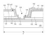
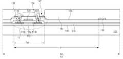
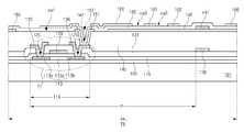
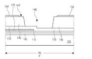
도 3은 본 발명의 실시예에 따른 터치 인셀 타입 액정표시장치용 어레이 기판에 있어 패드부 내의 하나의 데이터 패드전극이 형성된 부분에 대한 단면도.
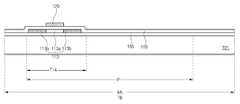
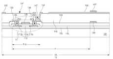
도 4는 본 발명의 실시예에 따른 터치 인셀 타입 액정표시장치용 어레이 기판에 있어 각 터치블럭 내에 서로 마주하는 x센싱배선과 센싱보조배선의 끝단이 위치한 부분에 대한 단면도.
도 5는 본 발명의 실시예에 따른 터치센서 인셀 타입 액정표시장치용 어레이 기판의 하나의 터치블럭에 대한 개략적인 평면도.
도 6a 내지 6j는 본 발명의 실시예에 따른 터치 인셀 타입 액정표시장치용 어레이 기판에 있어 스위칭 소자인 박막트랜지스터가 형성된 부분을 포함하여 하나의 화소영역에 대한 제조 단계별 공정 단면도.
도 7a 내지 7j는 본 발명의 실시예에 따른 터치 인셀 타입 액정표시장치용 어레이 기판에 있어 패드부 내의 하나의 데이터 패드전극이 형성되는 부분에 대한 제조 단계별 공정 단면도.
도 8a 내지 도 8j는 본 발명의 실시예에 따른 터치 인셀 타입 액정표시장치용 어레이 기판에 있어 각 터치블럭 내에 서로 마주하는 x센싱배선과 센싱보조배선의 끝단이 위치한 부분에 대한 단면도.1 is an exploded perspective view of a general liquid crystal display device.
2 is a cross-sectional view of one pixel region including a portion where a thin film transistor, which is a switching element, is formed in an array substrate for a touch-in-cell type liquid crystal display device according to an embodiment of the present invention.
3 is a cross-sectional view of a portion of the array substrate for a touch-in-cell type liquid crystal display according to an exemplary embodiment of the present invention where one data pad electrode is formed in the pad portion.
FIG. 4 is a cross-sectional view of a portion where an end of an x-sensing wiring and a sensing auxiliary wiring facing each other in each touch block in an array substrate for a touch-in-one type liquid crystal display device according to an embodiment of the present invention.
5 is a schematic plan view of one touch block of an array substrate for a touch sensor type in-cell type liquid crystal display according to an embodiment of the present invention.
FIGS. 6A to 6J are cross-sectional views illustrating steps of manufacturing a pixel region including a portion where a thin film transistor, which is a switching element, is formed in an array substrate for a touch-in-cell type liquid crystal display device according to an embodiment of the present invention.
FIGS. 7A to 7J are cross-sectional views illustrating steps of fabricating a portion of the array substrate for a touch-in-cell type liquid crystal display according to an exemplary embodiment of the present invention, in which one data pad electrode is formed.
8A to 8J are cross-sectional views of a portion where an end of an x-sensing wiring and a sensing auxiliary wiring, which face each other, are located in each touch block in an array substrate for a touch-in-one type liquid crystal display device according to an embodiment of the present invention.
이하, 본 발명에 따른 바람직한 실시예를 도면을 참조하여 설명한다.Hereinafter, preferred embodiments according to the present invention will be described with reference to the drawings.
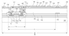
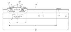
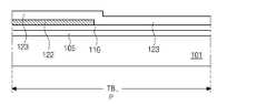
도 2는 본 발명의 실시예에 따른 터치 인셀 타입 액정표시장치용 어레이 기판에 있어 스위칭 소자인 박막트랜지스터가 형성된 부분을 포함하여 하나의 화소영역에 대한 단면도이며, 도 3은 본 발명의 실시예에 따른 터치 인셀 타입 액정표시장치용 어레이 기판에 있어 패드부 내의 하나의 데이터 패드전극이 형성된 부분에 대한 단면도이며, 도 4는 본 발명의 실시예에 따른 터치 인셀 타입 액정표시장치용 어레이 기판에 있어 각 터치블럭 내에 서로 마주하는 x센싱배선과 센싱보조배선의 끝단이 위치한 부분에 대한 단면도이다. 설명의 편의를 위해 각 화소영역(P) 내에 박막트랜지스터(Tr)가 형성되는 영역을 소자영역(TrA)이라 정의하였으며, 다수의 화소영역(P)을 하나의 단위영역인 터치블럭(TB)으로 정의하였다.FIG. 2 is a cross-sectional view of one pixel region including a portion where a thin film transistor as a switching element is formed in an array substrate for a touch-in-cell type liquid crystal display device according to an embodiment of the present invention. FIG. FIG. 4 is a cross-sectional view illustrating a portion of the array substrate for a touch-in-cell type liquid crystal display according to an embodiment of the present invention. Sectional view of the portion where the ends of the sensing wiring and sensing auxiliary wiring facing each other in the touch block are located. For convenience of description, a region where the thin film transistor Tr is formed in each pixel region P is defined as an element region TrA, and a plurality of pixel regions P are defined as a unit block of a touch block TB Respectively.
도시한 바와같이, 투명한 기판(101) 상에 무기절연물질 예를들면 산화실리콘(SiO2) 또는 질화실리콘(SiNx)서 이루어진 버퍼층(105)이 형성되어 있다. 이때, 상기 버퍼층(105)은 상기 투명한 기판(101)이 유리재질인 경우 500℃ 이상의 고온 공정 진행 시 유리재질의 투명한 기판(101)으로부터 나오는 알카리 이온에 의해 폴리실리콘의 반도체층(110)이 영향을 받아 박막트랜지스터(Tr)의 동작 특성의 저하가 발생할 수 있으므로 이를 방지하기 위해 형성하는 것으로 생략될 수도 있다.As shown in the figure, a
상기 버퍼층(105) 상부로 각 화소영역(P) 내의 소자영역(TrA)에는 순수 폴리실리콘으로 이루어지며 그 중앙부는 채널을 이루는 제 1 반도체 영역(113a) 그리고 상기 제 1 반도체 영역(113a) 양측면으로 고농도의 불순물이 도핑된 제 2 반도체 영역(113b)으로 구성된 반도체층(113)이 형성되어 있다.The device region TrA in each pixel region P above the
또한, 상기 반도체층(113)을 덮으며 전면에 무기절연물질로 이루어진 게이트 절연막(116)이 형성되어 있다.A
상기 게이트 절연막(116) 위로는 금속물질 예를들면 알루미늄(Al), 알루미늄 합금(AlNd), 구리(Cu), 구리합금, 몰리브덴(Mo), 몰리티타늄(MoTi) 중 어느 하나 또는 둘 이상의 물질로서 단일층 또는 다중층 구조를 가지며 상기 각 화소영역(P)의 경계에 대응하여 연결되며 일방향으로 연장하며 게이트 배선(미도시)이 형성되어 있다. 이때, 상기 게이트 절연막(116) 상에는 상기 게이트 배선(미도시)과 이격하여 각 터치블럭(TB) 별로 센싱보조배선(122)이 형성되고 있다.A metal material such as aluminum (Al), aluminum alloy (AlNd), copper (Cu), copper alloy, molybdenum (Mo), molybdenum (MoTi) (Not shown) having a single layer or a multilayer structure and connected in correspondence with the boundaries of the pixel regions P and extending in one direction. At this time, on the
본 발명은 터치 센서 인셀 타인 액정표시장치용 어레이 기판(101)이므로 터치센서(미도시)를 구비하여야 한다. 이러한 터치센서(미도시)는 통상 사용자의 손가락의 터치에 반응하는 것이므로 화소영역(P) 단위로 형성될 필요없이 다수의 화소영역(P)을 하나의 단위 즉 터치블럭(TB)으로 나누어 형성되는 것이다.Since the present invention is an
이러한 터치블럭의 구성에 대해서 도 5를 참조하여 간단히 설명한다.The configuration of the touch block will be briefly described with reference to FIG.
도 5는 본 발명의 실시예에 따른 터치센서 인셀 타입 액정표시장치용 어레이 기판의 하나의 터치블럭에 대한 개략적인 평면도이다.5 is a schematic plan view of one touch block of an array substrate for a touch sensor type in-cell type liquid crystal display according to an embodiment of the present invention.
다수의 화소영역(P)을 하나의 단위로 하여 구성되는 각 터치블럭(TB)은 그 내부가 크게 3개의 영역(A1, A2, A3)으로 나뉘고 있는 것이 특징이다. 이때 각 터치블럭(TB) 내에 구비된 3개의 영역(A1, A2, A3)은 게이트 배선(119)이 연장하는 방향으로 순차적으로 제 1, 2, 3 영역(A1, A2, A3)으로 나뉘어지고 있다.Each touch block TB, which is formed by a plurality of pixel regions P as one unit, is divided into three regions A1, A2, and A3. At this time, the three regions A1, A2, and A3 provided in each touch block TB are sequentially divided into the first, second, and third regions A1, A2, and A3 in the direction in which the
이때, 제 2 영역(A2)은 이의 상하로 이웃하는 터치블럭(TB)과 y센싱배선(ysl)을 통해 연결되고 있으며, 상기 제 2 영역(A2)을 기준으로 그 좌측 및 우측에 위치하는 상기 제 1 영역(A1)과 제 3 영역(A3)은 각각 이의 좌우로 위치하는 터치블럭(TB)과 x센싱배선(xsl)을 통해 연결되고 있는 것이 특징이다.At this time, the second area A2 is connected to the upper and lower touch blocks TB through the y sensing wiring ysl, and the second area A2 is connected to the left and right sides of the second area A2, The first area A1 and the third area A3 are connected to each other via a sensing block TB and an x sensing wiring xsl located on the left and right sides of the first area A1 and the third area A3.
즉, 각 터치블럭(TB) 내의 제 1 영역(A1)은 이의 좌측에 위치하는 터치블럭(TB)의 제 3 영역(A3)과 x센싱배선(xsl)을 통해 연결되고 있으며, 제 3 영역(A3)은 이의 우측에 위치하는 터치블럭(TB)의 제 1 영역(A1)과 x센싱배선(xsl)을 통해 연결되고 있다.That is, the first area A1 in each touch block TB is connected to the third area A3 of the touch block TB located on the left side thereof via the x sensing wiring xsl, and the third area A1 A3 are connected to the first area A1 of the touch block TB located on the right side thereof via the x sensing wiring xsl.
한편, 각 터치블럭(TB) 내에서 상기 제 2 영역(A2) 내에 구비된 x센싱배선(xsl)은 바(bar) 형태로 패터닝됨으로써 각각 이의 좌측 및 우측에 위치하는 제 1 및 제 3 영역(A1, A2)에 구비된 x센싱배선(xsl)과는 단선된 구성을 갖는 것이 특징이다.The x sensing wiring lines xsl provided in the second area A2 in each of the touch blocks TB are patterned in the form of a bar to form first and third regions (left and right) A1, and A2 are disconnected from each other.
즉, 상기 x센싱배선(xsl)은 각 터치블럭(TB) 내의 제 1 영역(A1)과 제 2 영역(A2)의 경계, 제 3 영역(A3)과 제 2 영역(A2)의 경계에서 단선된 형태를 이루고 있는 것이 특징이다.That is, the x sensing wiring xsl is connected to the first area A1 and the second area A2 in the respective touch blocks TB, and to the boundary between the third area A3 and the second area A2, It is characterized in that it is formed.
이때, x센싱배선(xsl) 자체로는 각 터치블럭(TB) 내에서 각 영역(A1, A2, A3)간의 경계에서 단선된 형태를 이루고 있지만, x센싱배선(xsl)은 전기적으로는 각 터치블럭(TB) 내에서 제 1 및 제 2 영역(A1, A2)간, 제 2 및 제 3 영역(A2, A3)간 연결되고 있는 것이 특징이다.At this time, although the x sensing wiring xsl itself is disconnected at the boundary between the areas A1, A2, and A3 in each touch block TB, the x sensing wiring xsl is electrically connected to each touch And is connected between the first and second regions A1 and A2 and between the second and third regions A2 and A3 within the block TB.
즉, 상기 제 1 영역(A1) 및 제 3 영역(A3) 내에 단선된 형태로 형성된 상기 x센싱배선(xsl)의 끝단은 각각 상기 게이트 절연막(미도시) 상에 상기 게이트 배선(119)과 이격하여 각 터치블럭(TB) 내의 제 2 영역(A2)에 형성되며 그 각각의 끝단이 각 터치블럭(TB) 내에서 제 1 및 제 3 영역(A1, A2)에 위치하는 센싱보조배선(122)의 끝단과 각각 상기 제 1 보호층(미도시)과, 제 2 보호층(미도시) 및 층간절연막(미도시)을 관통하며 서로 연결되며 형성된 제 2 및 제 1 센싱 콘택홀(158, 148)을 통해 접촉하고 있는 것이 특징이다.That is, the ends of the x sensing wiring (xsl) formed in the first area (A1) and the third area (A3) in a disconnected manner are separated from the gate wiring (119) on the gate insulating film And a sensing
이후에는 다시 도 2, 3, 4를 참조하여 단면 구성에 대해 설명한다. Hereinafter, the sectional configuration will be described with reference to Figures 2, 3, and 4 again.
한편, 상기 게이트 절연막(116) 위로는 상기 반도체층(113)의 제 1 반도체 영역(113a)에 대응하여 상기 게이트 배선(미도시)과 동일한 물질로 동일한 구조를 갖는 게이트 전극(120)이 형성되어 있다.On the
또한, 표시영역(AA) 외측의 비표시영역(NA)에는 게이트 절연막(116) 위로 상기 게이트 배선(미도시)의 일끝단과 연결되며 게이트 링크 배선(미도시)이 구비되고 있으며, 상기 비표시영역(NA) 중 패드부(PA)에는 상기 게이트 링크 배선(미도시)의 일끝단과 연결되며 게이트 패드전극(미도시)이 형성되고 있다.A non-display area NA outside the display area AA is connected to one end of the gate wiring (not shown) over the
다음, 상기 게이트 전극(120)과 게이트 배선(미도시)과 게이트 링크 배선(미도시) 및 게이트 패드전극(미도시) 위로 전면에 무기절연물질로 이루어진 층간절연막(123)이 형성되어 있다. 이때, 상기 층간절연막(123)과 그 하부에 위치하는 상기 게이트 절연막(116)에는 상기 제 1 반도체영역(113a) 양측에 각각 위치한 상기 제 2 반도체영역(113b) 각각을 노출시키는 반도체층 콘택홀(125)이 구비되고 있다.Next, an
다음, 상기 반도체층 콘택홀(125)을 구비한 상기 층간절연막(123) 상부에는 금속물질 예를들면 알루미늄(Al), 알루미늄 합금(AlNd), 구리(Cu), 구리합금, 몰리브덴(Mo), 몰리티타늄(MoTi) 중 어느 하나 또는 둘 이상의 물질로서 단일층 또는 다중층 구조로서 상기 게이트 배선(미도시)과 교차하여 화소영역(P)을 정의하는 데이터 배선(130)이 형성되고 있다. 이때, 상기 데이터 배선(130)이 다중층 구조를 이루는 경우 몰리브덴(Mo) 또는 몰리티타늄(MoTi)으로 이루어진 제 1 층과 알루미늄(Al), 알루미늄 합금(AlNd), 구리(Cu), 구리합금 중 어느 하나로 이루어진 제 2 층과 몰리브덴(Mo) 또는 몰리티타늄(MoTi)으로 이루어진 제 3 층의 3중층 구조로 이루어지는 것이 바람직하다. 도면에 있어서는 상기 데이터 배선(130)이 단일층 구조를 이루는 것을 일례로 나타내었다.Next, a metal material such as aluminum (Al), an aluminum alloy (AlNd), copper (Cu), a copper alloy, molybdenum (Mo), or a combination thereof is formed on the
또한, 상기 층간절연막(123) 위로 상기 소자영역(TrA)에는 상기 반도체층 콘택홀(125)을 통해 노출된 상기 제 2 반도체영역(113b)과 각각 접촉하며 상기 데이터 배선(130)과 동일한 물질로 동일한 구조를 가지며 서로 이격하는 소스 및 드레인 전극(133, 136)이 형성되어 있다.The device region TrA is in contact with the
이때, 상기 소자영역(TrA)에 순차 적층된 상기 반도체층(113)과 게이트 절연막(116)과 게이트 전극(120)과 층간절연막(123)과 서로 이격하는 소스 및 드레인 전극(133, 136)은 스위칭 소자인 박막트랜지스터(Tr)를 이룬다.At this time, the source and drain
한편, 상기 박막트랜지스터(Tr)는 상기 게이트 배선(미도시) 및 데이터 배선(130)과 전기적으로 연결되며 형성되어 있다. 즉, 상기 게이트 전극(120)은 상기 게이트 배선(미도시)과 연결되며 상기 소스 전극(133)은 상기 데이터 배선(130)과 연결되고 있다.The thin film transistor Tr is electrically connected to the gate line (not shown) and the
또한, 상기 비표시영역(NA)에 있어 상기 층간절연막(123) 상부에는 상기 데이터 배선(130)의 일끝단과 연결되며 데이터 링크배선(131)이 형성되고 있으며, 상기 패드부(PA)에는 상기 데이터 링크배선(131)의 일끝단과 연결되며 데이터 패드전극(132)이 형성되고 있다.In the non-display area NA, a data
다음, 상기 데이터 배선(130)과 소스 및 드레인 전극(133, 136) 상부로 표시영역 전면과 상기 비표시영역(NA) 중 패드부(PA)를 제외한 영역에는 유기절연물질 예를들면 포토아크릴 또는 벤조사이클로부텐로 이루어져 그 표면이 평탄한 상태를 이루는 제 1 보호층(145)이 형성되어 있다. 이때, 상기 제 1 보호층(145)은 패드부(PA)에 대해서는 형성되지 않으므로 패드부(PA)에 있어서는 상기 데이터 패드전극(132)과 이와 연결된 데이터 링크배선(131) 일부는 상기 제 1 보호층(145) 외측으로 노출된 상태가 된다.Next, an organic insulating material, for example, a photoacid or a metal oxide is formed on the entire surface of the display region and the non-display region NA except the pad portion PA above the
종래의 경우, 상기 데이터 배선과 소스 및 드레인 전극 상부에는 무기절연물질로 이루어진 보조 절연층이 형성된 후, 이의 상부에 전술한 바와같은 유기절연물질로 이루어진 제 1 보호층을 형성하고 있다. 이 경우 액정표시장치의 제조를 위해서는 보조 절연층 형성을 위한 무기절연물질의 사용이 지속적으로 발생됨으로써 비용 상승이 초래되고 있다.Conventionally, an auxiliary insulating layer made of an inorganic insulating material is formed on the data line, the source and drain electrodes, and a first protective layer made of the organic insulating material is formed on the auxiliary insulating layer. In this case, the use of the inorganic insulating material for forming the auxiliary insulating layer is continuously generated for the manufacture of the liquid crystal display device, thereby increasing the cost.
하지만, 본 발명에 따른 실시예에 있어서는 이러한 보조 절연층을 구성하지 않음으로서 재료비 저감의 효과를 갖는다. 이 경우 보조 절연층이 생략됨으로써 금속재질로 이루어진 데이터 배선(130)과 소스 및 드레인 전극(133, 136)이 직접적으로 유기절연물질로 이루어진 상기 제 1 보호층(145)과 접촉하게 되지만, 최근의 유기절연물질 특히 포토아크릴은 기술 발전이 이루어져 금속물질과도 접착력이 우수한 특성을 가지므로 무기절연물질로 이루어진 보조 절연층이 생략된다 하더라도 접합력 저하로 인한 문제는 발생하지 않는다.However, in the embodiment according to the present invention, the auxiliary insulating layer is not constituted, and the effect of reducing the material cost is obtained. In this case, the auxiliary insulating layer is omitted, so that the data wiring 130 made of a metal material and the source and drain
한편, 표시영역(AA)에 있어 상기 제 1 보호층(145)에는 상기 박막트랜지스터(Tr)의 드레인 전극(136)을 노출시키는 제 1 드레인 콘택홀(147)이 구비되고 있으며, 또한 각 터치블럭(TB) 내에 구비된 상기 각 센싱보조배선(122)의 끝단에 대응하는 층간절연막(123)을 노출시키는 제 1 센싱 콘택홀(148)이 구비되고 있다.The
다음, 상기 제 1 드레인 콘택홀(147) 및 제 1 센싱 콘택홀(148)을 갖는 제 1 보호층(145) 위로 투명 도전성 물질 인듐-틴-옥사이드(ITO) 또는 인듐-징크-옥사이드(IZO)로 이루어진 공통전극(150)이 표시영역(AA)에 대응하여 형성되고 있다.Next, a transparent conductive material indium-tin-oxide (ITO) or indium-zinc-oxide (IZO) is deposited on the
이때, 상기 공통전극(150)은 각 화소영역(P) 내의 소자영역(TrA)에 대응해서는 제 1 개구(oa1)가 형성됨으로써 상기 박막트랜지스터(Tr)를 노출시키도록 형성되고 있으며, 동시에 제 1 센싱 콘택홀(148)이 형성된 부분에 대응해서는 이보다 더 큰 면적을 갖는 제 2 개구(oa2)가 형성되고 있다.At this time, the
나아가 상기 공통전극(150)은 다수의 화소영역(P)을 하나의 단위로 한 터치블럭(TB) 별로 패터닝 된 형태로 형성되고 있는 것이 특징이다. 더욱이, 상기 공통전극(150)은 더욱 정확히는 터치블럭(TB) 내부에서 또 다시 제 1, 2 및 3 영역(도 5의 A1, A2, A3)별로 분리 형성되고 있는 것이 특징이다.In addition, the
한편, 본 발명의 실시예에 있어서 특징적인 구성으로서 상기 소자영역(TrA)에 구비된 상기 제 1 드레인 콘택홀(147) 내부를 포함하여 상기 제 1 드레인 콘택홀(147) 주변에는 상기 공통전극(150)을 이루는 동일한 물질로 이루어지며 상기 제 1 드레인 콘택홀(147) 내부에서 상기 드레인 전극(136)과 접촉하는 도전성 식각 방지패턴(151)이 형성되고 있다.As a characteristic feature of the embodiment of the present invention, the first
또한, 상기 제 1 보호층(145)이 형성되지 않은 패드부(PA)에 있어서는 상기 제 1 보호층(145) 외측으로 노출된 상기 데이터 링크배선(131) 일부와 상기 데이터 패드전극(132)에 대응하여 제 1 보조 패드 패턴(152)이 형성되고 있다.In the pad portion PA where the
이때, 상기 도전성 식각 방지패턴(151)은 이와 동일한 층에 형성된 상기 공통전극(150)과 이격하며 그 각각이 독립된 아일랜드 형태로 형성되고 있는 것이 특징이며, 상기 제 1 보조 패드 패턴(152) 또한 각각 상기 데이터 패드전극(132)에 대응하여 아일랜드 형태로 형성되고 있는 것이 특징이다.The
이렇게 상기 제 1 드레인 콘택홀(147)에 대응하여 투명 도전성 물질로 이루어진 상기 도전성 식각 방지패턴(151)을 형성하고, 패드부(PA)에 각 데이터 링크배선(131) 일부와 데이터 패드전극(132)에 대응하여 제 1 보조 패드 패턴(152)을 형성한 것은 투명 도전성 물질로 이루어진 상기 공통전극(150)의 패터닝 시 이를 식각하기 위한 식각액과 상기 데이터 배선(130)을 이루는 동일한 금속물질로 이루어지는 x, y 센싱배선(xsl, ysl)의 패터닝 시 이용되는 식각액에 상기 제 1 드레인 콘택홀(147)을 통해 노출된 드레인 전극(136)과, 상기 제 1 보호층(145) 외측으로 형성된 데이터 링크배선(131) 일부 및 데이터 패드전극(132)이 노출되는 것을 방지하기 위함이다.The conductive
또한, 터치블럭(TB) 별로 패터닝되어 형성된 상기 공통전극(150) 상기 데이터 배선(130)을 이루는 동일한 금속물질 예를들면 알루미늄(Al), 알루미늄 합금(AlNd), 구리(Cu), 구리합금, 몰리브덴(Mo), 몰리티타늄(MoTi) 중 어느 하나 또는 둘 이상의 물질로서 단일층 또는 다중층 구조로서 상기 게이트 배선(미도시)과 중첩하며 x센싱배선(xsl)이 형성되고 있으며, 상기 데이터 배선(130)과 중첩하며 y센싱배선(ysl)이 형성되고 있다.The
이때, 상기 x센싱배선(xsl)과 상기 y센싱배선(ysl)은 각 터치블럭(TB) 내의 제 1, 2 및 3 영역(도 5의 A1, A2, A3)역 상에서는 쇼트가 발생된 형태로 형성되지만, 각 터치블럭(TB) 내에서는 제 1 및 제 3 영역(도 5의 A1, A3)만이 전기적으로 연결되고, 제 2 영역(도 5의 TB)은 전기적으로 분리된 형태가 되며, 제 2 영역(도 5의 A2)은 데이터 배선(130)의 연장방향으로 이웃한 터치블럭(TB) 내의 제 2 영역(도 5의 A2)간에만 전기적으로 연결된 구성을 갖게 되므로 각 영역(도 5의 A1, A2, A3) 내에서 상기 x센싱배선(xsl)과 y센싱배선(ysl)이 쇼트된 구성을 갖는다 하여도 문제되지 않는다.At this time, the x sensing wiring xsl and the y sensing wiring ysl are formed in the first, second, and third regions (A1, A2, and A3 in FIG. 5) Only the first and third regions A1 and A3 of FIG. 5 are electrically connected, the second region TB of FIG. 5 is electrically isolated, and the third region 5) are electrically connected only to the second region (A2 in FIG. 5) in the neighboring touch block TB in the extension direction of the
한편, 상기 x센싱배선(xsl)은 각 터치블럭(TB) 내에서 그 끝단이 각각 상기 센싱보조배선(122)의 끝단에 대응하여 상기 층간절연막(123)을 노출시키는 제 1 센싱 콘택홀(148) 내부에 위치하고 있는 것이 특징이다.The x sensing wiring xsl is connected to the first
한편, 본 발명의 실시예에 따른 액정표시장치용 어레이 기판의 경우, 제 1 보호층(145) 외측으로 노출된 데이터 링크배선(131) 일부 및 데이터 패드전극(132)과, 상기 제 1 드레인 콘택홀(147)을 통해 노출된 드레인 전극(136)의 경우, 각각 제 1 보조 패드 패턴(152)과 도전성 식각 방지패턴(151)이 각각 구비됨으로써 상기 공통전극(150)과 접촉하는 상기 x센싱배선(도 5의 xsl)과 y센싱배선(ysl)을 패터닝 시 식각액에 상기 데이터 링크배선(131)과 데이터 패드전극(132) 및 드레인 전극(136)은 노출되지 않음으로 이들 구성요소가 식각액에 의해 손상되는 일은 발생되지 않음을 알 수 있다.In the case of the array substrate for a liquid crystal display according to an embodiment of the present invention, a part of the
다음, 상기 공통전극(150)과 x, y센싱배선(xsl, ysl) 상부로 전면에 무기절연물질 예를들면 산화실리콘(SiO2) 또는 질화실리콘(SiNx)으로서 제 2 보호층(155)이 형성되고 있다.Next, an inorganic insulating material such as silicon oxide (SiO2 ) or silicon nitride (SiN x) is formed on the entire surface of the
이때, 상기 제 2 보호층(155)에는 소자영역(TrA)에 있어서 상기 도전성 식각 방지패턴(151)을 노출시키는 제 2 드레인 콘택홀(157)이 구비되고 있으며, 상기 패드부(PA)에 있어서는 상기 데이터 패드전극(132)에 대응하여 제 1 보조 패드 패턴(152)을 각각 노출시키는 데이터 패드 콘택홀(159)이 구비되고 있다.The
또한, 상기 패드부(PA)에는 상기 제 2 보호층(155)과 더불어 층간절연막(123)까지 함께 패터닝됨으로써 상기 게이트 패드전극(미도시)을 노출시키는 게이트 패드 콘택홀(미도시)이 구비되고 있으며, 각 터치블럭(TB) 내부에는 상기 제 1 센싱 콘택홀(148)에 대응하여 이와 연결되는 형태로 상기 제 2 보호층(155)과 그 하부의 층간절연막(123)이 함께 패터닝됨으로써 각각 서로 인접하는 상기 보조센싱배선(122)의 일 끝단과 상기 x센싱배선(xsl)의 일 끝단을 동시에 노출시키는 제 2 센싱 콘택홀(158)이 구비되고 있다.A gate pad contact hole (not shown) for exposing the gate pad electrode (not shown) may be formed on the pad portion PA by patterning the
다음, 상기 제 2 보호층(155) 위로는 투명 도전성 물질 예를들면 인듐-틴-옥사이드(ITO) 또는 인듐-징크-옥사이드(IZO)각 화소영역(P) 내에 상기 제 2 드레인 콘택홀(157)을 통해 상기 드레인 전극(136)과 접촉하는 도전성 식각 방지패턴(151)과 접촉하는 화소전극(160)이 각각 형성되고 있다. 이때, 상기 화소전극(160)에는 다수의 바(bar) 형태의 제 3 개구(op3)가 구비됨으로서 구동전압 인가 시 상기 공통전극(150)과 더불어 프린지 필드를 발생시키게 된다.The
또한, 패드부(PA)에 있어서는 상기 화소전극(160)을 이루는 동일한 물질로서 상기 제 2 보호층(155) 위로 상기 게이트 패드 콘택홀(미도시)을 통해 각각의 상기 게이트 패드전극(미도시)과 접촉하는 보조 게이트 패드전극(미도시)이 형성되고 있으며, 상기 데이터 패드 콘택홀(159)을 통해 상기 제 1 보조 패드 패턴(152)과 접촉하며 보조 데이터 패드전극(165)이 형성되고 있다.In the pad portion PA, the gate pad electrode (not shown) is formed on the
또한, 각 터치블럭(TB) 내부에는 각각 상기 제 2 센싱 콘택홀(158)을 통해 노출된 상기 센싱보조배선(122)의 일끝단과 x센싱배선(xsl)의 일끝단과 동시에 접촉하는 연결패턴(163)이 아일랜드 형태로 구비됨으로써 본 발명의 실시예에 따른 터치센서 인셀 타입 액정표시장치용 어레이 기판이 완성되고 있다.Inside each of the touch blocks TB, a connection pattern (not shown) which simultaneously contacts one end of the sensing
이러한 구성에 의해 실질적으로 각 터치블럭(TB) 내에서 제 1, 2, 3 영역(도 5의 A1, A2, A3)에서 x센싱배선(xsl)이 상기 y센싱배선(ysl)과 쇼트없이 전기적으로 연결된 상태를 이루게 된다.With this configuration, the x sensing wiring xsl in the first, second, and third regions A1, A2, and A3 in each touch block TB is electrically and electrically connected to the y sensing wiring ysl As shown in FIG.
이때, 상기 각 화소영역(P)에 구비된 상기 화소전극(160)과 상기 공통전극(150)은 상기 제 2 보호층(155)을 개재하여 중첩하도록 형성되고 있으며, 중첩하는 상기 공통전극(150)과 제 2 보호층(155)과 화소전극(160)은 스토리지 커패시터를 이룬다.
The
이후에는 전술한 구성을 갖는 터치센서 인셀 타입 액정표시장치용 어레이 기판의 제조 방법에 대해 설명한다.Hereinafter, a method of manufacturing an array substrate for a touch sensor type in-cell type liquid crystal display device having the above-described configuration will be described.
도 6a 내지 6j는 본 발명의 실시예에 따른 터치 인셀 타입 액정표시장치용 어레이 기판에 있어 스위칭 소자인 박막트랜지스터가 형성된 부분을 포함하여 하나의 화소영역에 대한 제조 단계별 공정 단면도이며, 도 7a 내지 7j는 본 발명의 실시예에 따른 터치 인셀 타입 액정표시장치용 어레이 기판에 있어 패드부 내의 하나의 데이터 패드전극이 형성되는 부분에 대한 제조 단계별 공정 단면도이며, 도 8a 내지 도 8j는 본 발명의 실시예에 따른 터치 인셀 타입 액정표시장치용 어레이 기판에 있어 각 터치블럭 내에 서로 마주하는 x센싱배선과 센싱보조패턴의 끝단이 위치한 부분에 대한 제조 단계별 공정 단면도이다.FIGS. 6A to 6J are cross-sectional views illustrating steps of manufacturing a pixel region including a portion where a thin film transistor, which is a switching element, is formed in an array substrate for a touch-in-cell type liquid crystal display device according to an embodiment of the present invention, FIGS. 8A to 8J are cross-sectional views illustrating a method of fabricating an array substrate for a touch-sensitive type liquid crystal display according to an exemplary embodiment of the present invention, Sectional view of a portion of the array substrate for a touch in cell type liquid crystal display according to an embodiment of the present invention.
우선, 도 6a, 7a 및 8a에 도시한 바와같이, 투명한 기판(101) 상에 무기절연물질 예를 들면 산화실리콘(SiO2) 또는 질화실리콘(SiNx)을 증착하여 버퍼층(105)을 형성한다.6A, 7A and 8A, an inorganic insulating material such as silicon oxide (SiO2 ) or silicon nitride (SiNx) is deposited on a
상기 버퍼층(105)은 비정질 실리콘을 폴리 실리콘으로 재결정화 할 경우, 레이저 조사 또는 열처리 시에 의해 발생하는 열로 인해 기판(101) 내부에 존재하는 알칼리 이온, 예를 들면 칼륨 이온(K+), 나트륨 이온(Na+) 등이 발생할 수 있는데, 이러한 알칼리 이온에 의해 폴리실리콘으로 이루어진 반도체층의 막특성이 저하되는 것을 방지하기 위함이다. 이때, 상기 버퍼층(105)은 생략할 수 있다.When the amorphous silicon is recrystallized into polysilicon, the
다음, 상기 버퍼층(105) 위로 순수 비정질 실리콘을 증착하여 순수 비정질 실리콘층(미도시)을 형성하고, 엑시머 레이저를 이용한 ELA(Excimer Laser Annealing)법, SLS(Sequential lateral Solidification) 결정화법, 열 결정화법, 교번자장 결정화(Alternating Magnetic Field Crystallization : AMFC) 중 어느 하나의 결정화 공정을 진행함으로써 상기 비정질 실리콘층(미도시)을 폴리실리콘층(미도시)으로 결정화한다.Next, a pure amorphous silicon layer (not shown) is formed by depositing pure amorphous silicon on the
이후, 마스크 공정을 실시하여 상기 폴리실리콘층(미도시)을 패터닝함으로써 상기 각 화소영역(P)내의 소자영역(TrA)에 각각 순수 폴리실리콘 상태의 반도체층(113)을 형성한다.Thereafter, a mask process is performed to pattern the polysilicon layer (not shown) to form a
다음, 도 6b, 7b 및 8b에 도시한 바와같이, 상기 순수 폴리실리콘의 반도체층(113) 위로 무기절연물질 예를들면 산화실리콘(SiO2) 또는 질화실리콘(SiNx)을 증착하여 게이트 절연막(116)을 형성한다.Next, as shown in FIGS. 6B, 7B and 8B, an inorganic insulating material such as silicon oxide (SiO2 ) or silicon nitride (SiNx) is deposited on the
다음, 상기 게이트 절연막(116) 위로 금속물질 예를들면 알루미늄(Al), 알루미늄 합금(AlNd), 구리(Cu), 구리합금, 몰리브덴(Mo), 몰리티타늄(MoTi) 중 어느 하나 또는 둘 이상의 물질로서 단일층 또는 다중층 구조를 갖는 제 1 금속층(미도시)을 형성한다.Next, a metal material such as aluminum (Al), aluminum alloy (AlNd), copper (Cu), copper alloy, molybdenum (Mo), molybdenum (MoTi) A first metal layer (not shown) having a single layer or a multilayer structure is formed.
이후, 상기 제 1 금속층(미도시)을 마스크 공정을 실시하여 패터닝함으로써 상기 각 반도체층(113)의 중앙부에 대응하여 게이트 전극(120)을 각각 형성하고, 동시에 상기 게이트 절연막(116) 위로 상기 화소영역(P)의 경계에 상기 소자영역(TrA)에 형성된 게이트 전극(120)과 연결되며 일 방향으로 연장하는 게이트 배선(미도시)과 각 터치블럭(TB) 별로 상기 게이트 배선(미도시)과 나란하게 이격하며 센싱보조배선(122)을 형성한다.Thereafter, the first metal layer (not shown) is masked and patterned to form
이때, 도면에 나타내지 않았지만, 비표시영역(NA)에는 상기 게이트 배선(미도시)의 일끝단과 연결된 게이트 링크배선(미도시)을 형성하고, 동시에 패드부(PA)에는 상기 게이트 링크배선(미도시)의 일끝단과 연결된 게이트 패드전극(미도시)을 형성한다.At this time, a gate link wiring (not shown) connected to one end of the gate wiring (not shown) is formed in the non-display area NA, and at the same time, the gate wiring A gate pad electrode (not shown) connected to one end of the gate electrode (not shown) is formed.
다음, 도 6c, 7c 및 8c에 도시한 바와같이, 상기 각 게이트 전극(120)을 블록킹 마스크로 이용하여 상기 기판(101) 전면에 불순물을 도핑함으로써 상기 반도체층(113) 중 상기 게이트 전극(120) 외측에 위치한 부분에 상기 불순물이 도핑된 제 2 반도체영역(113b)을 이루도록 하고, 블록킹됨으로써 상기 불순물의 도핑이 방지된 게이트 전극(120)에 대응하는 부분은 순수 폴리실리콘의 제 1 반도체영역(113a)을 이루도록 한다.Next, as shown in FIGS. 6C, 7C, and 8C, impurities are doped on the entire surface of the
다음, 도 6d, 7d 및 8d에 도시한 바와같이, 상기 제 1 및 제 2 반도체영역(113a, 113b)으로 나뉘어진 반도체층(113) 위로 전면에 무기절연물질 예를들면 질화실리콘(SiNx) 또는 산화실리콘(SiO2)을 증착하여 전면에 층간절연막(123)을 형성 한다.Next, as shown in FIGS. 6D, 7D and 8D, an inorganic insulating material such as silicon nitride (SiNx) or silicon nitride (SiNx) is formed on the entire surface of the
이후, 상기 층간절연막(123)을 패터닝함으로써 상기 각 반도체층(113)의 제 2 반도체영역(113b)을 각각 노출시키는 반도체층 콘택홀(125)을 형성한다.Then, the
다음, 도 6e, 7e 및 8e에 도시한 바와같이, 상기 반도체 콘택홀(125)과 제 1 센싱 콘택홀이 구비된 상기 층간절연막(123) 위로 금속물질 예를들면 알루미늄(Al), 알루미늄 합금(AlNd), 구리(Cu), 구리합금, 몰리브덴(Mo), 몰리티타늄(MoTi) 중 어느 하나 또는 둘 이상의 물질로서 단일층 또는 다중층 구조의 제 2 금속층(미도시)을 형성한다.Next, as shown in FIGS. 6E, 7E, and 8E, a metal material such as aluminum (Al), an aluminum alloy (Al), or the like is formed on the
이후, 상기 제 2 금속층(미도시)을 패터닝함으로써 패터닝함으로써 상기 소자영역(TrA)에 상기 반도체층 콘택홀(125)을 통해 상기 제 2 영역(113b)과 각각 접촉하며 서로 이격하는 소스 및 드레인 전극(133, 136)을 형성 한다. 이때, 상기 각 화소영역(P) 내의 소자영역(TrA)에 구비된 상기 반도체층(113)과 게이트 절연막(116)과 게이트 전극(120)과 층간절연막(123)과 서로 이격하는 소스 및 드레인 전극(133, 136)은 스위칭 소자인 박막트랜지스터(Tr)를 이룬다.Thereafter, patterning is performed by patterning the second metal layer (not shown) to form source and drain
동시에 상기 층간절연막(123) 위로 상기 화소영역(P)의 경계에 상기 소자영역(TrA)에 형성된 소스 전극(133)과 연결되며 상기 게이트 배선(미도시)과 교차하는 데이터 배선(130)을 형성한다.At the same time, a
또한, 비표시영역(NA)에는 상기 층간절연막(123) 위로 상기 데이터 배선(130)과 연결된 데이터 링크배선(131)을 형성하고, 패드부(PA)에는 상기 층간절연막(123) 위로 상기 데이터 링크배선(131)과 연결된 데이터 패드전극(132)을 형성한다.A data
다음, 도 6f, 7f 및 8f에 도시한 바와같이, 상기 박막트랜지스터(Tr)와 데이터 배선(130)과 데이터 링크배선(131) 및 데이터 패드전극(132) 위로 표시영역(AA) 전면과 비표시영역(NA) 중 패드부(PA)를 제외한 영역에 유기절연물질 예를들면 포토아크릴(photo acryl) 또는 벤조사이클로부텐(BCB)을 도포하여 그 표면이 평탄한 형태를 갖는 제 1 보호층(145)을 형성한다.Next, as shown in FIGS. 6F, 7F, and 8F, a front surface of the display area AA and a non-display area (not shown) are formed on the thin film transistor Tr and the data wiring 130, the
이후, 상기 제 1 보호층(145)에 대해 마스크 공정을 진행하여 패터닝함으로써 상기 각 소자영역(TrA)에 있어 상기 드레인 전극(136)을 노출시키는 제 1 드레인 콘택홀(147)을 형성하고, 동시에 각 터치블럭(TB)에 있어서 상기 센싱보조배선(122)의 일끝단에 대응하는 상기 층간절연막(123)을 노출시키는 제 1 센싱 콘택홀(148)을 형성한다.Thereafter, a mask process is performed on the
다음, 도 6g, 7g 및 8g에 도시한 바와같이, 상기 제 1 드레인 콘택홀(147)과 제 1 센싱 콘택홀(148)을 갖는 제 1 보호층(145) 위로 투명 도전성 물질 예를 들면, 인듐-틴-옥사이드(ITO) 또는 인듐-징크-옥사이드(IZO)를 전면에 증착하고, 이를 패터닝함으로서 각 터치블럭(TB) 별로 이격하는 형태의 공통전극(150)을 형성 한다.Next, as shown in FIGS. 6G, 7G, and 8G, a transparent conductive material, for example, indium (In), is deposited on the
이때, 상기 공통전극(150)은 각 소자영역(TrA)에 대해서는 제 1 개구(oa1)를 가지며, 상기 센싱보조배선(122)의 양 끝단이 위치하는 부분 즉, 제 1 센싱 콘택홀(148)이 형성된 부분에 대응해서는 상기 제 1 센싱 콘택홀(148) 보다 더 큰 면적을 갖는 제 2 개구(oa2)를 갖도록 형성하는 것이 특징이다.At this time, the
이는 상기 제 2 드레인 콘택홀(157)을 통해 드레인 전극(136)과 접촉하는 화소전극(160)과 상기 공통전극(150), 추후 형성되는 제 2 센싱 콘택홀(157)을 통해 상기 센싱보조배선(122) 및 x센싱배선(xsl)을 전기적으로 연결시키는 연결패턴(미도시)과 상기 공통전극(150) 간의 쇼트를 방지하기 위함이다.This is accomplished through the
또한, 동시에 각 소자영역(TrA)에는 상기 제 1 드레인 콘택홀(147) 내부 및 이의 주변에 상기 공통전극(150)과 이격하는 도전성 식각 방지패턴(151)을 형성하고, 상기 패드부(PA)에는 상기 제 1 보호층(145) 외측으로 노출된 상기 데이터 링크배선(131)과 데이터 패드전극(132)에 대응하여 이들 구성요소 보다 더 큰 폭을 가져 이들 구성요소 각각을 완전히 덮는 아일랜드 형태로서 제 1 보조 패드 패턴(152)을 형성한다.At the same time, in each device region TrA, a conductive
이렇게 도전성 식각 방지패턴(151)과 제 1 보조 패드 패턴(152)을 형성하는 것은, 추후 공정에서 식각액에 노출되어 손상되는 것을 방지하기 위함이다.The formation of the conductive
다음, 도 6h, 7h 및 8h에 도시한 바와같이, 상기 공통전극(150)과 도전성 식각 방지패턴(151) 및 제 1 보조 패드 패턴(152) 위로 금속물질 예를 들면 알루미늄(Al), 알루미늄 합금(AlNd), 구리(Cu), 구리합금, 몰리브덴(Mo), 몰리티타늄(MoTi) 중 어느 하나 또는 둘 이상의 물질로서 단일층 또는 다중층 구조를 갖는 제 3 금속층(미도시)을 형성한다.Next, as shown in FIGS. 6H, 7H, and 8H, a metal material such as aluminum (Al), an aluminum alloy (Al), or the like is formed on the
이후, 상기 제 3 금속층을 패터닝함으로써 도 5를 통해 설명한 바와 같은 평면 형태를 가지며 각각 상기 게이트 배선(미도시) 및 데이터 배선(130)과 중첩하는 x센싱배선(xsl) 및 y센싱배선(ysl)을 형성한다.Thereafter, the third metal layer is patterned to form an x-sensing wiring xsl and a y-sensing wiring ysl which have a planar shape as described with reference to Fig. 5 and overlap the gate wiring (not shown) and the data wiring 130, .
이때, 상기 x센싱배선(xsl)은 각 터치블럭(TB) 별로 단선된 형태를 가지며 단선된 부분의 끝단은 필요시 절곡 형성되어 상기 제 1 센싱 콘택홀(148) 내부에서 상기 센싱보조배선(122)의 끝단과 인접하여 위치하도록 형성하는 것이 특징이다.At this time, the x sensing wiring xsl is disconnected for each of the touch blocks TB, and the ends of the disconnected portions are bent if necessary so that the sensing
본 발명의 실시예의 경우, 상기 x, y센싱배선(xsl, ysl) 형성 시 이를 패터닝하기 위한 식각액에 노출시키는 과정에서 상기 제 1 보호층(145)이 형성되지 않거나 제거된 부분을 통해 노출되는 구성요소 일례로 드레인 전극(136)과 데이터 링크배선(131) 및 데이터 패드전극(132)은 이들 구성요소와 완전 중첩하는 형태로 각각 도전성 식각 방지패턴(151) 및 제 1 보조 패드 패턴(152)이 각각 형성되고 있으므로 상기 x,y센싱배선(xsl, ysl) 패터닝을 위한 식각액에 이들 구성요소는 전혀 노출되지 않음으로 종래와 같이 별도의 무기절연물질로 이루어진 보조 절연층을 형성하지 않고도 식각액에 의한 손상을 방지할 수 있는 것이 특징이다.In the embodiment of the present invention, when the x and y sensing wirings (xsl, ysl) are formed, the
다음, 도 6i, 7i 및 8i에 도시한 바와같이, 상기 x센싱배선(xsl)과 y센싱배선(ysl) 위로 무기절연물질 예를 들면 산화실리콘(SiO2) 또는 질화실리콘(SiNx)을 증착하여 표시영역과 비표시영역(NA) 전면에 제 2 보호층(155)을 형성한다.6I, 7i and 8i, an inorganic insulating material such as silicon oxide (SiO2 ) or silicon nitride (SiN x) is deposited on the x sensing wiring (xsl) and the y sensing wiring (ysl) The second
이후 상기 제 2 보호층(155)을 패터닝함으로써 상기 제 1 드레인 콘택홀(147)과 연결되어 상기 드레인 전극(136)과 접촉하는 도전성 식각 방지패턴(151)을 노출시키는 제 2 드레인 콘택홀(157)을 형성하고, 상기 패드부(PA)에 있어서는 상기 데이터 패드전극(132)에 대응해서는 상기 제 1 보조 패드 패턴(152)을 노출시키는 제 2 데이터 패드 콘택홀(159)을 형성한다.A second
동시에 상기 제 1 센싱 콘택홀(148)에 대응하는 부분 및 패드부(PA)에 있어서는 상기 제 2 보호층(155)과 더불어 그 하부에 위치하는 층간절연막(123)까지 함께 패터닝함으로서 상기 제 1 센싱 콘택홀(148)에 대응해서는 상기 제 1 센싱 콘택홀(148) 내부에서 상기 센싱보조배선(122)의 일끝단과 이와 인접하는 상기 x센싱배선(xsl)의 일 끝단을 동시에 노출시키는 제 2 센싱 콘택홀(158)을 형성하고, 상기 게이트 패드전극(미도시)에 대응해서는 상기 게이트 패드전극(미도시)을 노출시키는 게이트 패드 콘택홀(미도시)을 형성한다.At the same time, in the portion corresponding to the first
다음, 도 6j, 7j 및 8j에 도시한 바와같이, 상기 제 2 드레인 콘택홀(157)과 게이트 및 데이터 패드 콘택홀(미도시, 159) 및 제 2 센싱 콘택홀(158)이 구비된 상기 제 2 보호층(155) 위로 투명 도전성 물질 예를 들면, 인듐-틴-옥사이드(ITO) 또는 인듐-징크-옥사이드(IZO)를 증착하여 투명 도전성 물질층(미도시)을 형성한다.Next, as shown in FIGS. 6J, 7J and 8J, the second
이후, 상기 투명 도전성 물질층(미도시)을 패터닝함으로서 각 화소영역(P) 내에 상기 제 2 드레인 콘택홀(157)을 통해 상기 도전성 식각 방지패턴(151)과 접촉하는 화소전극(160)을 형성한다.The
또한, 동시에 상기 각 터치블럭(TB) 내에는 상기 서로 연결된 제 1 및 제 2 센싱 콘택홀(148, 158) 내부에 상기 센싱보조배선(122)의 일끝단과 이와 인접하는 상기 x센싱배선(xsl)의 일끝단과 동시에 접촉하는 연결패턴(163)을 형성한다.At the same time, in the respective touch blocks TB, one end of the sensing
또한, 패드부(PA)에 있어서는 상기 게이트 패드 콘택홀(미도시)을 통해 상기 게이트 패드전극(미도시)과 접촉하는 보조 게이트 패드전극(미도시)을 형성하고, 동시에 상기 데이터 패드 콘택홀(159)을 통해 상기 제 1 보조 패드 패턴(152)과 접촉하는 보조 데이터 패드전극(165)을 형성함으로써 본 발명의 실시예에 따른 터치센서 인셀타입 액정표시장치용 어레이 기판을 완성한다.In the pad portion PA, an auxiliary gate pad electrode (not shown) is formed to contact the gate pad electrode (not shown) through the gate pad contact hole (not shown), and at the same time, 159 to form an auxiliary
이때, 상기 각 화소전극(160)은 그 하부에 위치한 공통전극(150)과 프린지 필드 형성을 위해 각 화소영역(P)내에 일정간격 이격하는 바(bar) 형태의 다수의 제 3 개구(oa3)를 갖도록 형성하는 것이 특징이다.Each of the
이렇게 완성된 본 발명의 실시예에 따른 터치센서 인셀타입 액정표시장치용 어레이 기판(101)에는 컬러필터 기판(미도시)과 액정층(미도시)을 구비하여 액정표시장치(미도시)를 이룬 후, 가로 및 세로방향으로 배열된 터치블럭(TB)의 끝단에 각각 x센싱배선(xsl)과 y센싱배선(ysl)과 각각 연결되도록 X방향 센싱회로(미도시)와 Y방향 센싱회로(미도시)를 실장함으로써 표시영역(AA) 내에 터치가 발생되면 공통전극(150)과 화소전극(160) 사이에 발생된 커패시턴스 변화를 통해 터치 발생을 감지하고 이를 전압형태로 바꾸어 x센싱배선(xsl)과 y센싱배선(ysl)을 통해 상기 X방향 센싱회로(미도시)와 Y방향 센싱회로(미도시)로 각각 전달되고 이러한 구동에 의해 표시영역(AA) 내에 터치가 발생된 부분의 위치를 인식하게 되며, 터치가 발생된 부분에 연관된 동작을 실시하게 된다.The
101 : 기판 105 : 버퍼층
113 : 반도체층 113a, 113b : 제 1 및 제 2 반도체영역
116 : 게이트 절연막 120 : 게이트 전극
123 : 층간절연막 125 : 반도체층 콘택홀
130 : 데이터 배선 133 : 소스 전극
136 : 드레인 전극 145 : 제 1 보호층
147 : 제 1 드레인 콘택홀 150 : 공통전극
151 : 도전성 식각 방지패턴 155 : 제 2 보호층
157 : 제 2 드레인 콘택홀 160 : 화소전극
AA : 표시영역 oa1, oa3 : 제 1 및 제 3 개구
P : 화소영역 TB : 터치블록
Tr : 박막트랜지스터 TrA : 소자 영역
ysl : y센싱배선101: substrate 105: buffer layer
113:
116: gate insulating film 120: gate electrode
123: interlayer insulating film 125: semiconductor layer contact hole
130: data line 133: source electrode
136: drain electrode 145: first protective layer
147: first drain contact hole 150: common electrode
151: conductive etching prevention pattern 155: second protection layer
157: second drain contact hole 160: pixel electrode
AA: display area oa1, oa3: first and third openings
P: pixel area TB: touch block
Tr: thin film transistor TrA: element region
ysl: y sensing wiring
Claims (22)
Translated fromKorean상기 각 화소영역 내에 상기 게이트 및 데이터 배선과 연결되며 형성된 박막트랜지스터와;
유기절연물질로 이루어지며, 상기 박막트랜지스터 위로 상기 박막트랜지스터의 드레인 전극을 노출시키는 제 1 드레인 콘택홀 형성된 제 1 보호층과;
상기 제 1 보호층 위로 상기 각 터치블럭 별로 이격하며 형성된 공통전극과;
상기 제 1 보호층 위로 상기 공통전극과 이격하며 상기 제 1 드레인 콘택홀과 중첩하며 상기 공통전극을 이루는 동일한 물질로 형성된 도전성 식각 방지패턴과;
상기 공통전극 위로 상기 게이트 배선과 중첩하도록 형성된 x센싱배선 및 상기 데이터 배선과 중첩하도록 형성된 y센싱배선과;
상기 공통전극과 x센싱배선 및 y센싱배선 위로 상기 기판 전면에 형성되며, 상기 도전성 식각 방지패턴을 노출시키는 제 2 드레인 콘택홀을 가지며 형성된 제 2 보호층과;
상기 제 2 보호층 위로 상기 제 2 드레인 콘택홀을 통해 상기 도전성 식각 방지패턴과 접촉하며 상기 각 화소영역 별로 형성되며, 다수의 바(bar) 형태의 개구를 갖는 화소전극
을 포함하며, 상기 비표시영역에는 패드부가 정의되며, 상기 비표시영역에는 상기 게이트 배선이 형성된 동일한 층에 상기 게이트 배선과 연결된 게이트 링크배선이 형성되며, 상기 패드부에는 상기 게이트 링크배선과 연결된 게이트 패드전극이 형성되고, 상기 비표시영역에는 상기 데이터 배선이 형성된 동일한 층에 상기 데이터 배선과 연결된 데이터 링크배선이 형성되며, 상기 패드부에는 상기 데이터 링크배선과 연결된 데이터 패드전극이 형성되며, 상기 제 1 보호층은 상기 패드부를 노출시키며 형성되며, 상기 제 1 보호층 외측으로 노출된 상기 각 데이터 패드전극을 완전히 덮으며 상기 공통전극을 이루는 동일한 물질로 제 1 보조 패드 패턴이 형성된 것이 특징인 터치센서 인셀 타입 액정표시장치용 어레이 기판.
A display device, comprising: a display area having a plurality of pixel areas; a non-display area defined outside the plurality of pixel areas; and a plurality of touch blocks having a plurality of pixel blocks in the display area, A gate and a data line formed to intersect with each other through the gate and the data line;
A thin film transistor formed in each of the pixel regions and connected to the gate and the data line;
A first protective layer formed of an organic insulating material and having a first drain contact hole exposing a drain electrode of the thin film transistor on the thin film transistor;
A common electrode formed on the first protection layer and spaced apart from each other by the touch blocks;
A conductive etch stopping pattern formed on the first passivation layer and spaced apart from the common electrode and formed of the same material as the common electrode overlapping the first drain contact hole;
An x sensing wiring formed to overlap the gate wiring over the common electrode, and a y sensing wiring formed to overlap the data wiring;
A second passivation layer formed on the common electrode, the x sensing wiring, and the y sensing wiring over the entire surface of the substrate, the second passivation layer having a second drain contact hole exposing the conductive etch stop pattern;
A plurality of pixel electrodes having a plurality of bar-shaped openings formed in the respective pixel regions in contact with the conductive etching prevention pattern through the second drain contact holes over the second passivation layer,
Wherein a pad portion is defined in the non-display region, a gate link wiring connected to the gate wiring is formed in the same layer in which the gate wiring is formed, and the pad portion is formed with a gate A pad electrode is formed in the non-display region, a data link wiring connected to the data wiring is formed in the same layer where the data wiring is formed, a data pad electrode connected to the data link wiring is formed in the pad portion, 1 protection layer is formed to expose the pad portion and a first auxiliary pad pattern is formed of the same material completely covering the data pad electrodes exposed to the outside of the first protection layer and forming the common electrode, An array substrate for an in-cell type liquid crystal display device.
상기 각 터치블럭은 상기 게이트 배선의 연장방향으로 이웃한 터치블럭과 상기 x센싱배선에 의해 연결되며,
상기 각 터치블럭은 이격하는 제 1 및 제 3 영역과, 상기 제 1 및 제 3 영역 사이에 상기 데이터 배선의 연장방향으로 이웃한 터치블럭과 상기 y센싱배선에 의해 연결된 제 2 영역으로 구성되며,
상기 공통전극은 상기 각 터치블럭 내에서 상기 제 1, 2, 3 영역별로 분리 형성된 것이 특징인 터치센서 인셀 타입 액정표시장치용 어레이 기판.
The method according to claim 1,
Wherein each of the touch blocks is connected to a touch block neighboring the gate wiring by an x sensing wiring,
Each of the touch blocks includes first and third regions which are spaced apart from each other and a second region which is connected between the first and third regions by a touch block neighboring the extending direction of the data line and the y-
Wherein the common electrode is divided into the first, second, and third regions within the respective touch blocks.
상기 터치블럭 내에서 상기 제 1 및 제 3 영역에 형성된 상기 x센싱배선은 상기 제 1 영역과 제 2 영역의 경계, 상기 제 2 영역과 제 3 영역의 경계에서는 끊긴 형태로 이격하며 형성된 것이 특징인 터치센서 인셀 타입 액정표시장치용 어레이 기판.
3. The method of claim 2,
Wherein the x sensing wiring formed in the first and third regions in the touch block is formed so as to be spaced apart from a boundary between the first region and the second region and a boundary between the second region and the third region, An array substrate for a touch sensor in-cell type liquid crystal display.
상기 게이트 전극은 상기 제 1 절연막의 하부에 상기 데이터 배선은 상기 제 1 절연막의 상부에 형성되며,
상기 제 1 절연막 상에 상기 게이트 배선과 나란하게 상기 게이트 배선이 형성된 층에 상기 게이트 배선과 동일한 물질로 상기 각 터치블럭별로 형성된 센싱보조배선을 포함하며,
상기 각 터치블럭 내에서 상기 x센싱배선과 상기 센싱보조배선이 연결되며 형성된 것이 특징인 터치센서 인셀 타입 액정표시장치용 어레이 기판.
The method of claim 3,
Wherein the gate electrode is formed on the lower portion of the first insulating film, the data wiring is formed on the first insulating film,
And a sensing auxiliary wiring formed on the first insulating film in the layer in which the gate wiring is formed in parallel with the gate wiring, the sensing wiring being formed for each of the touch blocks with the same material as the gate wiring,
And the x sensing wiring and the sensing auxiliary wiring are connected to each other in each of the touch blocks.
상기 제 1 보호층에는 상기 각 터치블럭 별로 상기 x센싱배선의 끝단에 대응하는 상기 제 1 절연막을 노출시키는 제 1 콘택홀이 구비되며,
상기 제 2 보호층에는 상기 제 1 콘택홀 내부에서 상기 x센싱배선의 끝단을 노출시키는 제 2 콘택홀이 구비되며,
상기 제 1 절연막에는 상기 제 1 콘택홀이 연장된 형태로 상기 센싱보조배선의 끝단을 노출시키는 제 3 콘택홀이 구비되며,
서로 연결된 상기 제 2 및 제 3 콘택홀을 통해 노출된 상기 x센싱배선의 끝단과 상기 센싱보조배선의 끝단은 상기 화소전극을 이루는 동일한 물질로 이루어진 연결패턴과 동시에 접촉하며 형성된 것이 특징인 터치센서 인셀 타입 액정표시장치용 어레이 기판.
5. The method of claim 4,
Wherein the first protection layer is provided with a first contact hole exposing the first insulating film corresponding to an end of the x sensing wiring for each of the touch blocks,
And a second contact hole exposing the end of the x sensing wiring in the first contact hole is formed in the second protection layer,
A third contact hole exposing an end of the sensing auxiliary wiring in the form of extending the first contact hole is formed in the first insulating film,
And the ends of the x-sensing wiring and the sensing auxiliary wiring exposed through the second and third contact holes connected to each other are simultaneously in contact with a connection pattern made of the same material constituting the pixel electrode. Type liquid crystal display device.
상기 공통전극은 상기 박막트랜지스터가 형성된 부분에 대응하여 제 1 개구가 형성되며, 상기 제 1 콘택홀에 대응하여 상기 제 1 콘택홀보다 더 큰 면적을 갖는 제 2 개구가 형성된 것이 특징인 터치센서 인셀 타입 액정표시장치용 어레이 기판.
6. The method of claim 5,
Wherein the common electrode has a first opening corresponding to a portion where the thin film transistor is formed and a second opening corresponding to the first contact hole and having a larger area than the first contact hole is formed, Type liquid crystal display device.
상기 터치블럭 중 상기 게이트 배선의 연장방향으로 동일한 라인상에 형성되는 상기 터치블럭은 상기 x센싱배선에 의해 모두 전기적으로 연결되며,
상기 터치블럭 중 상기 데이터 배선의 연장방향으로 동일한 라인 상에 형성되는 상기 터치블럭은 상기 y센싱배선에 의해 모두 전기적으로 연결되도록 형성된 것이 특징인 터치센서 인셀 타입 액정표시장치용 어레이 기판.
The method according to claim 6,
The touch blocks formed on the same line in the extending direction of the gate lines of the touch blocks are all electrically connected by the x sensing wiring,
Wherein the touch blocks formed on the same line in the extending direction of the data lines are all electrically connected by the y sensing wiring.
상기 제 2 보호층에는 상기 제 1 보조 패드 패턴을 노출시키는 데이터 패드 콘택홀이 구비되며,
상기 제 2 보호층과 상기 제 1 절연막에는 상기 게이트 패드전극을 노출시키는 게이트 패드 콘택홀이 구비되며,
상기 제 2 보호층 상부에는 상기 화소전극을 이루는 동일한 물질로 상기 데이터 패드 콘택홀을 통해 상기 제 1 보조 패드 패턴과 접촉하는 보조 데이터 패드전극과, 상기 게이트 패드 콘택홀을 통해 상기 게이트 패드전극과 접촉하는 보조 게이트 패드전극이 형성된 것이 특징인 터치센서 인셀 타입 액정표시장치용 어레이 기판.
The method according to claim 1,
And a data pad contact hole exposing the first auxiliary pad pattern is formed in the second protection layer,
And a gate pad contact hole exposing the gate pad electrode is formed in the second passivation layer and the first insulating layer,
An auxiliary data pad electrode which is in contact with the first auxiliary pad pattern through the data pad contact hole with the same material forming the pixel electrode on the second passivation layer and an auxiliary data pad electrode which contacts the gate pad electrode through the gate pad contact hole, And an auxiliary gate pad electrode is formed on the substrate.
상기 박막트랜지스터는 제 2 절연막 상에 순차 적층된 형태로 순수 폴리실리콘의 제 1 반도체영역과 이의 양측에 불순물이 도핑된 폴리실리콘의 제 2 반도체층으로 구성된 반도체층과, 게이트 절연막과, 상기 제 1 반도체영역에 대응하여 게이트 전극과, 상기 제 2 반도체영역을 노출시키는 반도체층 콘택홀을 구비한 상기 제 1 절연막과, 서로 이격하며 상기 제 2 반도체영역과 각각 접촉하는 소스 및 드레인 전극으로 구성된 것이 특징인 터치센서 인셀 타입 액정표시장치용 어레이 기판.
The method according to claim 1,
Wherein the thin film transistor comprises a semiconductor layer composed of a first semiconductor region of pure polysilicon and a second semiconductor layer of polysilicon doped with impurities on both sides thereof in the form of sequentially stacked on a second insulating film, The first insulating film having a gate electrode corresponding to a semiconductor region, a semiconductor layer contact hole exposing the second semiconductor region, and source and drain electrodes spaced apart from each other and contacting the second semiconductor region, respectively In touch sensor In-cell type LCD array substrate.
상기 공통전극과 상기 화소전극은 투명 도전성 물질로 이루어진 것이 특징인 터치센서 인셀 타입 액정표시장치용 어레이 기판.
6. The method according to claim 1 or 5,
Wherein the common electrode and the pixel electrode are made of a transparent conductive material.
상기 x센싱배선 및 y센싱배선은 상기 데이터 배선을 이루는 동일한 물질로 이루어진 것이 특징인 터치센서 인셀 타입 액정표시장치용 어레이 기판.
The method according to claim 1,
Wherein the x-sensing wiring and the y-sensing wiring are made of the same material as the data wiring.
상기 박막트랜지스터 위로 유기절연물질로 이루어지며 상기 박막트랜지스터 위로 상기 박막트랜지스터의 드레인 전극을 노출시키는 제 1 드레인 콘택홀이 구비된 제 1 보호층을 형성하는 단계와;
상기 제 1 보호층 위로 상기 각 터치블럭 별로 이격하는 공통전극과, 상기 공통전극과 이격하며 상기 제 1 드레인 콘택홀에 대응하여 상기 제 1 드레인 콘택홀보다 더 넓은 면적으로 가지며 상기 드레인 전극과 완전히 중첩하는 도전성 식각 방지패턴을 형성하는 단계와;
상기 공통전극 위로 상기 게이트 배선과 중첩하는 x센싱배선 및 상기 데이터 배선과 중첩하는 y센싱배선을 형성하는 단계와;
상기 공통전극과 x센싱배선 및 y센싱배선 위로 전면에 상기 도전성 식각 방지패턴을 노출시키는 제 2 드레인 콘택홀이 구비된 제 2 보호층을 형성하는 단계와;
상기 제 2 보호층 위로 상기 제 2 드레인 콘택홀을 통해 상기 도전성 식각 방지패턴과 접촉하며 각 화소영역 별로 다수의 바(bar) 형태의 개구를 갖는 화소전극을 형성하는 단계를 포함하며, 상기 비표시영역에는 패드부가 정의되며, 상기 게이트 배선을 형성하는 단계는 상기 비표시영역에 상기 게이트 배선과 연결된 게이트 링크배선을 형성하고 동시에 상기 패드부에 상기 게이트 링크배선과 연결된 게이트 패드전극을 형성하는 단계를 포함하며, 상기 데이터 배선을 형성하는 단계는 상기 비표시영역에 상기 데이터 배선과 연결된 데이터 링크배선을 형성하고 동시에 상기 패드부에 상기 데이터 링크배선과 연결된 데이터 패드전극을 형성하는 단계를 포함하며, 상기 제 1 보호층은 상기 패드부를 노출시키도록 형성하며, 상기 공통전극을 형성하는 단계는 상기 제 1 보호층 외측으로 노출된 상기 각 데이터 패드전극에 대응하여 상기 각 데이터 패드전극을 완전히 덮는 제 1 보조 패드 패턴을 형성하는 단계를 포함하는 것이 특징인 터치센서 인셀 타입 액정표시장치용 어레이 기판의 제조 방법.
A display device, comprising: a display area having a plurality of pixel areas; a non-display area defined outside the plurality of pixel areas; and a plurality of touch blocks having a plurality of pixel blocks in the display area, Forming a gate wiring and a data wiring intersecting with each other via a gate electrode and a thin film transistor connected to the two wirings;
Forming a first passivation layer over the thin film transistor, the first passivation layer being made of an organic insulating material and having a first drain contact hole exposing a drain electrode of the thin film transistor over the thin film transistor;
A common electrode spaced from the common electrode by the touch block on the first passivation layer; and a second electrode formed on the common electrode and having a larger area than the first drain contact hole and completely overlapping the drain electrode, Forming a conductive etch-preventive pattern;
Forming an x sensing wiring overlying the gate wiring over the common electrode and a y sensing wiring overlapping the data wiring;
Forming a second passivation layer on the entire surface of the common electrode, the x sensing wiring, and the y sensing wiring, the second passivation layer having a second drain contact hole exposing the conductive etch stop pattern;
Forming a pixel electrode having a plurality of bar-shaped openings in each pixel region in contact with the conductive etching prevention pattern through the second drain contact hole over the second passivation layer, Wherein the step of forming the gate wiring includes forming a gate link wiring connected to the gate wiring in the non-display area and forming a gate pad electrode connected to the gate wiring wiring in the pad part, Wherein forming the data line includes forming a data link line connected to the data line in the non-display area and forming a data pad electrode connected to the data line line in the pad area, The first protective layer may be formed to expose the pad portion, Forming a first auxiliary pad pattern that completely covers the data pad electrodes corresponding to the respective data pad electrodes exposed to the outside of the first passivation layer. / RTI >
상기 각 터치블럭은 상기 게이트 배선의 연장방향으로 이웃한 터치블럭과 상기 x센싱배선에 의해 연결되며,
상기 각 터치블럭은 이격하는 제 1 및 제 3 영역과, 상기 제 1 및 제 3 영역 사이에 상기 데이터 배선의 연장방향으로 이웃한 터치블럭과 상기 y센싱배선에 의해 연결된 제 2 영역으로 구성되며,
상기 공통전극은 상기 각 터치블럭 내에서 상기 제 1, 2, 3 영역별로 분리 형성하는 것이 특징인 터치센서 인셀 타입 액정표시장치용 어레이 기판의 제조 방법.
14. The method of claim 13,
Wherein each of the touch blocks is connected to a touch block neighboring the gate wiring by an x sensing wiring,
Each of the touch blocks includes first and third regions which are spaced apart from each other and a second region which is connected between the first and third regions by a touch block neighboring the extending direction of the data line and the y-
Wherein the common electrode is separately formed in each of the first, second, and third regions in each of the touch blocks.
상기 터치블럭 내에서 상기 제 1 및 제 3 영역에 형성된 상기 x센싱배선은 상기 제 1 영역과 제 2 영역의 경계, 상기 제 2 영역과 제 3 영역의 경계에서는 끊긴 형태로 이격하도록 형성하는 것이 특징인 터치센서 인셀 타입 액정표시장치용 어레이 기판의 제조 방법.
15. The method of claim 14,
The x sensing wiring formed in the first and third regions in the touch block is formed so as to be spaced apart from the boundary between the first region and the second region and between the second region and the third region A method of manufacturing an array substrate for an in - touch sensor in - cell type liquid crystal display device.
상기 게이트 전극은 상기 제 1 절연막의 하부에 상기 데이터 배선은 상기 제 1 절연막의 상부에 형성하며,
상기 게이트 배선을 형성하는 단계는 상기 제 1 절연막 상에 상기 게이트 배선과 나란하게 상기 각 터치블럭별로 센싱보조배선을 형성하는 단계를 포함하며,
상기 각 터치블럭 내에서 상기 x센싱배선과 상기 센싱보조배선이 연결되도록 형성하는 것이 특징인 터치센서 인셀 타입 액정표시장치용 어레이 기판의 제조 방법.
16. The method of claim 15,
Wherein the gate electrode is formed under the first insulating film and the data line is formed on the first insulating film,
Wherein forming the gate wiring includes forming a sensing auxiliary wiring for each of the touch blocks on the first insulating film in parallel with the gate wiring,
And the sensing wiring and the sensing auxiliary wiring are connected to each other in each of the touch blocks. The method of manufacturing an array substrate for an in-cell type liquid crystal display according to claim 1,
상기 제 1 보호층을 형성하는 단계는, 상기 각 터치블럭 별로 상기 x센싱배선의 끝단에 대응하는 상기 제 1 절연막을 노출시키는 제 1 콘택홀이 구비되도록 하며,
상기 제 2 보호층을 형성하는 단계는, 상기 제 1 콘택홀 내부에서 상기 x센싱배선의 끝단을 노출시키는 제 2 콘택홀이 구비되도록 하며,
상기 제 1 절연막을 형성하는 단계는, 상기 제 1 콘택홀이 연장된 형태로 상기 센싱보조배선의 끝단을 노출시키는 제 3 콘택홀이 구비되도록 하며,
상기 화소전극을 형성하는 단계는, 서로 연결된 상기 제 2 및 제 3 콘택홀을 통해 노출된 상기 x센싱배선의 끝단과 상기 센싱보조배선의 끝단과 동시에 접촉하는 연결패턴을 형성하는 단계를 포함하는 것이 특징인 터치센서 인셀 타입 액정표시장치용 어레이 기판의 제조 방법.
17. The method of claim 16,
The forming of the first passivation layer may include forming a first contact hole exposing the first insulating film corresponding to an end of the x sensing wiring for each of the touch blocks,
The forming of the second passivation layer may include forming a second contact hole exposing an end of the x sensing wiring in the first contact hole,
The forming of the first insulating layer may include forming a third contact hole exposing the end of the sensing auxiliary wiring in the form of extending the first contact hole,
The forming of the pixel electrode may include forming a connection pattern that contacts the ends of the x sensing wiring and the sensing auxiliary wiring exposed through the second and third contact holes connected to each other at the same time A method of manufacturing an array substrate for an in-cell type liquid crystal display device.
상기 공통전극은 상기 박막트랜지스터가 형성된 부분에 대응하여 제 1 개구를 가지며, 상기 제 1 콘택홀에 대응하여 상기 제 1 콘택홀보다 더 큰 면적을 갖는 제 2 개구가 구비되도록 형성하는 것이 특징인 터치센서 인셀 타입 액정표시장치용 어레이 기판의 제조 방법.
18. The method of claim 17,
Wherein the common electrode has a first opening corresponding to a portion where the thin film transistor is formed and a second opening corresponding to the first contact hole and having a larger area than the first contact hole, Method of manufacturing array substrate for sensor insensitive type liquid crystal display device.
상기 터치블럭 중 상기 게이트 배선의 연장방향으로 동일한 라인상에 형성되는 터치블럭은 상기 x센싱배선에 의해 모두 전기적으로 연결되며,
상기 터치블럭 중 상기 데이터 배선의 연장방향으로 동일한 라인 상에 형성되는 터치블럭은 상기 y센싱배선에 의해 모두 전기적으로 연결되도록 형성하는 것이 특징인 터치센서 인셀 타입 액정표시장치용 어레이 기판의 제조 방법.
19. The method of claim 18,
The touch blocks formed on the same line in the extension direction of the gate lines among the touch blocks are all electrically connected by the x sensing lines,
Wherein the touch blocks formed on the same line in the extending direction of the data lines are electrically connected to each other by the y sensing wiring.
상기 제 2 보호층을 형성하는 단계는, 상기 제 1 보조 패드 패턴을 노출시키는 데이터 패드 콘택홀과, 상기 제 2 보호층 더불어 이의 하부에 위치하는 상기 제 1 절연막을 동시에 패터닝함으로써 상기 게이트 패드전극을 노출시키는 게이트 패드 콘택홀을 형성하는 단계를 포함하며,
상기 화소전극을 형성하는 단계는, 상기 제 2 보호층 상부에 상기 데이터 패드 콘택홀을 통해 상기 제 1 보조 패드 패턴과 접촉하는 보조 데이터 패드전극과, 상기 게이트 패드 콘택홀을 통해 상기 게이트 패드전극과 접촉하는 보조 게이트 패드전극을 형성하는 단계를 포함하는 것이 특징인 터치센서 인셀 타입 액정표시장치용 어레이 기판의 제조 방법.
14. The method of claim 13,
The forming of the second passivation layer may include patterning the gate pad electrode by simultaneously patterning a data pad contact hole exposing the first auxiliary pad pattern and the first insulating layer located under the second passivation layer, Forming a gate pad contact hole that exposes the gate pad,
The forming of the pixel electrode may include forming an auxiliary data pad electrode over the second passivation layer and contacting the first auxiliary pad pattern through the data pad contact hole and a second data pad electrode contacting the gate pad electrode through the gate pad contact hole, And forming an auxiliary gate pad electrode in contact with the substrate.
상기 박막트랜지스터를 형성하는 단계는,
제 1 절연막 상에 순수 비정질 실리콘층을 형성하는 단계와;
상기 순수 비정질 실리콘층을 폴리실리콘층으로 결정화하는 단계와;
상기 폴리실리콘층을 패터닝하여 폴리실리콘의 반도체층을 형성하는 단계와;
상기 폴리실리콘의 반도체층 위로 게이트 절연막을 형성하는 단계와;
상기 게이트 절연막 위로 상기 폴리실리콘의 반도체층의 중앙부에 상기 게이트 배선과 연결된 게이트 전극을 형성하는 단계와;
상기 게이트 전극을 도핑 마스크로 하여 불순물 도핑을 실시하여 상기 게이트 전극 외측으로 노출된 부분의 상기 반도체층을 불순물 폴리실리콘층으로 변경하는 단계와;
상기 게이트 전극 위로 상기 게이트 전극 양측으로 상기 불순물 폴리실리콘의 반도체층을 각각 노출시키는 반도체층 콘택홀을 갖는 상기 제 1 절연막을 형성하는 단계와;
상기 제 1 절연막 위로 상기 반도체층 콘택홀을 통해 상기 불순물 폴리실리콘의 반도체층과 각각 접촉하는 소스 전극 및 상기 드레인 전극을 형성하는 단계
를 포함하는 터치센서 인셀 타입 액정표시장치용 어레이 기판의 제조 방법.14. The method of claim 13,
Wherein forming the thin film transistor comprises:
Forming a pure amorphous silicon layer on the first insulating film;
Crystallizing the pure amorphous silicon layer into a polysilicon layer;
Patterning the polysilicon layer to form a semiconductor layer of polysilicon;
Forming a gate insulating film over the semiconductor layer of the polysilicon;
Forming a gate electrode connected to the gate wiring on a central portion of the semiconductor layer of polysilicon over the gate insulating film;
Performing impurity doping using the gate electrode as a doping mask to change the semiconductor layer of the portion exposed to the outside of the gate electrode to an impurity polysilicon layer;
Forming a first insulating film having a semiconductor layer contact hole exposing a semiconductor layer of the impurity polysilicon on both sides of the gate electrode over the gate electrode;
A source electrode which contacts the semiconductor layer of the impurity polysilicon via the semiconductor layer contact hole over the first insulating film, and a step of forming the drain electrode
Type liquid crystal display device.
Priority Applications (5)
| Application Number | Priority Date | Filing Date | Title |
|---|---|---|---|
| KR1020110037243AKR101520423B1 (en) | 2011-04-21 | 2011-04-21 | Touch sensor in-cell type liquid crystal display device and method of fabricating the same |
| DE102011088319.3ADE102011088319B4 (en) | 2011-04-21 | 2011-12-12 | A substrate for a liquid crystal display device having a touch-sensitive sensor in the cells and a manufacturing method thereof |
| CN201110415413.2ACN102750024B (en) | 2011-04-21 | 2011-12-13 | Substrate for in-cell type touch sensor liquid crystal display device and method of fabricating the same |
| US13/333,053US9201533B2 (en) | 2011-04-21 | 2011-12-21 | Substrate for in-cell type touch sensor liquid crystal display device and method of fabricating the same |
| US14/930,902US9465246B2 (en) | 2011-04-21 | 2015-11-03 | Substrate for in-cell type touch sensor liquid crystal display device and method of fabricating the same |
Applications Claiming Priority (1)
| Application Number | Priority Date | Filing Date | Title |
|---|---|---|---|
| KR1020110037243AKR101520423B1 (en) | 2011-04-21 | 2011-04-21 | Touch sensor in-cell type liquid crystal display device and method of fabricating the same |
Publications (2)
| Publication Number | Publication Date |
|---|---|
| KR20120119369A KR20120119369A (en) | 2012-10-31 |
| KR101520423B1true KR101520423B1 (en) | 2015-05-14 |
Family
ID=46967463
Family Applications (1)
| Application Number | Title | Priority Date | Filing Date |
|---|---|---|---|
| KR1020110037243AActiveKR101520423B1 (en) | 2011-04-21 | 2011-04-21 | Touch sensor in-cell type liquid crystal display device and method of fabricating the same |
Country Status (4)
| Country | Link |
|---|---|
| US (2) | US9201533B2 (en) |
| KR (1) | KR101520423B1 (en) |
| CN (1) | CN102750024B (en) |
| DE (1) | DE102011088319B4 (en) |
Families Citing this family (90)
| Publication number | Priority date | Publication date | Assignee | Title |
|---|---|---|---|---|
| KR101295533B1 (en)* | 2010-11-22 | 2013-08-12 | 엘지디스플레이 주식회사 | Liquid crystal display device and Method for manufacturing the same |
| KR101830179B1 (en)* | 2011-11-03 | 2018-02-21 | 삼성디스플레이 주식회사 | Organic Light Emitting Diode Display Device |
| WO2013073495A1 (en)* | 2011-11-18 | 2013-05-23 | シャープ株式会社 | Active matrix substrate, liquid crystal display device and method for manufacturing active matrix substrate |
| KR101971594B1 (en) | 2012-02-16 | 2019-04-24 | 삼성디스플레이 주식회사 | Thin film trannsistor array panel and manufacturing method thereof |
| US9869908B2 (en)* | 2012-03-06 | 2018-01-16 | Apple Inc. | Pixel inversion artifact reduction |
| US8704232B2 (en) | 2012-06-12 | 2014-04-22 | Apple Inc. | Thin film transistor with increased doping regions |
| US9065077B2 (en) | 2012-06-15 | 2015-06-23 | Apple, Inc. | Back channel etch metal-oxide thin film transistor and process |
| JP2014021170A (en)* | 2012-07-12 | 2014-02-03 | Panasonic Liquid Crystal Display Co Ltd | Liquid crystal display device and manufacturing method thereof |
| US9685557B2 (en) | 2012-08-31 | 2017-06-20 | Apple Inc. | Different lightly doped drain length control for self-align light drain doping process |
| US8987027B2 (en) | 2012-08-31 | 2015-03-24 | Apple Inc. | Two doping regions in lightly doped drain for thin film transistors and associated doping processes |
| US8748320B2 (en) | 2012-09-27 | 2014-06-10 | Apple Inc. | Connection to first metal layer in thin film transistor process |
| US8999771B2 (en) | 2012-09-28 | 2015-04-07 | Apple Inc. | Protection layer for halftone process of third metal |
| US9201276B2 (en) | 2012-10-17 | 2015-12-01 | Apple Inc. | Process architecture for color filter array in active matrix liquid crystal display |
| WO2014073483A1 (en)* | 2012-11-08 | 2014-05-15 | シャープ株式会社 | Active matrix substrate and display device using same |
| US9599866B2 (en)* | 2012-11-08 | 2017-03-21 | Sharp Kabushiki Kaisha | Active matrix substrate and display device |
| US9594281B2 (en)* | 2012-11-30 | 2017-03-14 | Semiconductor Energy Laboratory Co., Ltd. | Liquid crystal display device |
| CN103278955B (en)* | 2012-12-14 | 2015-11-11 | 上海天马微电子有限公司 | Color film substrate and touch liquid crystal display device |
| CN103293750B (en)* | 2012-12-14 | 2016-05-11 | 上海天马微电子有限公司 | Embedded touch screen color film substrate and manufacturing method thereof |
| CN103034386B (en)* | 2012-12-20 | 2015-11-11 | 北京京东方光电科技有限公司 | Capacitance type touch control display panel, display device, control device and method |
| KR102052749B1 (en)* | 2012-12-20 | 2019-12-06 | 엘지디스플레이 주식회사 | Touch sensor integrated type display device |
| KR101697272B1 (en)* | 2012-12-24 | 2017-01-17 | 엘지디스플레이 주식회사 | Array Substrate for Liquid Crystal Display and Method for Fabricating The Same |
| KR102104356B1 (en)* | 2012-12-24 | 2020-04-24 | 엘지디스플레이 주식회사 | Array substrate for fringe field switching mode liquid crystal display device and Method of fabricating the same |
| KR102047727B1 (en)* | 2012-12-29 | 2019-11-22 | 엘지디스플레이 주식회사 | Touch sensor in-cell type liquid crystal display device and method of fabricating the same |
| JP5909198B2 (en) | 2013-01-21 | 2016-04-26 | 株式会社ジャパンディスプレイ | Liquid crystal display panel and electronic device |
| US9001297B2 (en) | 2013-01-29 | 2015-04-07 | Apple Inc. | Third metal layer for thin film transistor with reduced defects in liquid crystal display |
| US9088003B2 (en) | 2013-03-06 | 2015-07-21 | Apple Inc. | Reducing sheet resistance for common electrode in top emission organic light emitting diode display |
| US9639193B2 (en) | 2013-04-25 | 2017-05-02 | Beijing Boe Optoelectronics Technology Co., Ltd. | Touch-control pixel driving circuit, touch-control pixel driving method, array substrate and liquid crystal display (LCD) device |
| CN103235457B (en)* | 2013-04-25 | 2014-11-19 | 北京京东方光电科技有限公司 | Touch pixel driving circuit, method, array substrate and liquid crystal display device |
| CN103941496B (en)* | 2013-05-13 | 2017-06-06 | 上海天马微电子有限公司 | Array substrate, touch liquid crystal display panel and manufacturing method thereof |
| CN104216545A (en)* | 2013-05-31 | 2014-12-17 | 京东方科技集团股份有限公司 | In-cell touch device and implementation method thereof |
| KR102066020B1 (en)* | 2013-06-28 | 2020-01-14 | 엘지디스플레이 주식회사 | Array substrate for display device having oxide semiconductor and method for fabricating the same |
| KR102068170B1 (en)* | 2013-08-19 | 2020-01-21 | 엘지디스플레이 주식회사 | Thin film transistor substrate and Method of manufacturing the same |
| KR102066592B1 (en)* | 2013-09-27 | 2020-02-11 | 엘지디스플레이 주식회사 | Display Device and Method of manufacturing the same |
| KR102198111B1 (en)* | 2013-11-04 | 2021-01-05 | 삼성디스플레이 주식회사 | Thin film transistor array panel and manufacturing method thereof |
| KR102082265B1 (en)* | 2013-11-28 | 2020-02-27 | 엘지디스플레이 주식회사 | Touch sensor integrated type display device |
| KR102140644B1 (en)* | 2013-12-11 | 2020-08-04 | 삼성디스플레이 주식회사 | Thin film transistor substrate and manufacturing method of thin film transistor substrate |
| CN103700669A (en)* | 2013-12-19 | 2014-04-02 | 京东方科技集团股份有限公司 | Array substrate and preparation method thereof as well as display device |
| KR102167136B1 (en)* | 2013-12-31 | 2020-10-16 | 엘지디스플레이 주식회사 | Display device having thin film transistor array substrate and method for fabricating the same |
| KR101584423B1 (en)* | 2014-02-21 | 2016-01-11 | 하이디스 테크놀로지 주식회사 | Touch Panel with Overcoat Layer for reducing Moire, Liquid Crystal Display Device Having the Touch Panel and Method For Forming the Touch Panel |
| CN105022184A (en)* | 2014-04-17 | 2015-11-04 | 株式会社日本显示器 | Display device |
| CN203894716U (en)* | 2014-04-21 | 2014-10-22 | 速博思股份有限公司 | Embedded touch display device with three-dimensional space configuration sensing block |
| CN104020621B (en)* | 2014-05-26 | 2017-03-01 | 京东方科技集团股份有限公司 | A kind of array base palte and preparation method thereof, display device |
| US9753590B2 (en) | 2014-06-13 | 2017-09-05 | Lg Display Co., Ltd. | Display device integrated with touch screen panel and method of fabricating the same |
| KR101725896B1 (en)* | 2014-06-13 | 2017-04-12 | 엘지디스플레이 주식회사 | Display device integrated with touch screen panel and method for fabricating the same |
| CN104076550A (en)* | 2014-06-17 | 2014-10-01 | 京东方科技集团股份有限公司 | Color film array substrate, display device and method for manufacturing color film array substrate |
| KR101719397B1 (en)* | 2014-08-14 | 2017-03-24 | 엘지디스플레이 주식회사 | Touch sensor integrated type liquid crystal display device |
| KR102256461B1 (en)* | 2014-10-10 | 2021-05-26 | 삼성디스플레이 주식회사 | Touch sensor and display including the same |
| KR101661039B1 (en) | 2014-12-30 | 2016-10-11 | 엘지디스플레이 주식회사 | Ultra High Resolution Flat Panel Display Having In-Cell Type Touch Sensor |
| CN104503619B (en)* | 2014-12-31 | 2017-09-05 | 深圳市华星光电技术有限公司 | The manufacture method and touch-screen of a kind of array base palte |
| KR102297760B1 (en)* | 2014-12-31 | 2021-09-03 | 엘지디스플레이 주식회사 | Liquid crystal display device with oxide thin film transistor |
| CN104571715B (en)* | 2015-02-02 | 2018-01-02 | 京东方科技集团股份有限公司 | Array base palte and preparation method thereof and driving method, display device |
| CN104867944B (en) | 2015-05-08 | 2018-07-10 | 深圳市华星光电技术有限公司 | Array base-plate structure and preparation method thereof |
| CN104777692B (en) | 2015-05-08 | 2018-09-04 | 厦门天马微电子有限公司 | Array substrate and production method, touch-control display panel |
| TWI561894B (en)* | 2015-05-29 | 2016-12-11 | Hon Hai Prec Ind Co Ltd | Manufacturing method of making electronic connection structure, tft substrate, and insulation layer |
| US10228787B2 (en)* | 2015-06-05 | 2019-03-12 | Innolux Corporation | Display device |
| KR102326122B1 (en)* | 2015-09-03 | 2021-11-12 | 동우 화인켐 주식회사 | Touch panel and image display device comprising the same |
| CN105116276B (en)* | 2015-09-15 | 2019-03-01 | 深圳市华星光电技术有限公司 | A kind of detection device of capacitance plate |
| CN105070268B (en)* | 2015-09-23 | 2017-10-24 | 深圳市华星光电技术有限公司 | Reduce the method and apparatus of the leakage current of embedded touch LCD panel |
| KR101750428B1 (en)* | 2015-09-24 | 2017-06-23 | 엘지디스플레이 주식회사 | Display device including touch screen function |
| KR102521944B1 (en)* | 2015-10-02 | 2023-04-18 | 삼성디스플레이 주식회사 | Head mounted display and fabrication method thereof |
| CN105259690A (en)* | 2015-10-10 | 2016-01-20 | 武汉华星光电技术有限公司 | Manufacturing method of array substrate, array substrate, and touch control liquid crystal display apparatus |
| CN108352138B (en)* | 2015-11-06 | 2020-09-29 | 夏普株式会社 | Display substrate and display device |
| KR102401063B1 (en) | 2015-11-10 | 2022-05-24 | 엘지디스플레이 주식회사 | Backplane Substrate Having In-cell Type Touch Panel, and Liquid Crystal Display Device Using the Same and Method for Manufacturing the Same |
| KR102392683B1 (en)* | 2015-11-30 | 2022-05-02 | 엘지디스플레이 주식회사 | Display device with a built-in touch screen |
| KR102543487B1 (en) | 2015-12-28 | 2023-06-16 | 삼성디스플레이 주식회사 | Self capacitance touch screen and display device having the same |
| KR102431688B1 (en)* | 2015-12-31 | 2022-08-11 | 엘지디스플레이 주식회사 | Array substrate with enhanced thermal resistance and display device having thereof |
| KR102485387B1 (en)* | 2016-01-20 | 2023-01-06 | 삼성디스플레이 주식회사 | Display device |
| KR102435900B1 (en)* | 2016-01-21 | 2022-08-26 | 삼성디스플레이 주식회사 | Display device |
| CN105742238A (en)* | 2016-03-02 | 2016-07-06 | 京东方科技集团股份有限公司 | Pore structure and array substrate, manufacturing methods of pore structure and array substrate, detection device and display device |
| TWI686653B (en)* | 2016-05-16 | 2020-03-01 | 日商凸版印刷股份有限公司 | Display device |
| CN105931986A (en)* | 2016-05-18 | 2016-09-07 | 京东方科技集团股份有限公司 | Array substrate manufacturing method, array substrate and display apparatus |
| US10101853B2 (en) | 2016-06-03 | 2018-10-16 | Apple Inc. | Display with shallow contact holes and reduced metal residue at planarization layer steps |
| WO2018073706A1 (en) | 2016-10-21 | 2018-04-26 | Semiconductor Energy Laboratory Co., Ltd. | Display device and operating method thereof |
| KR102036293B1 (en)* | 2017-03-22 | 2019-10-24 | 동우 화인켐 주식회사 | Electrode connection structure and touch sensor |
| CN106896609B (en) | 2017-04-28 | 2019-11-19 | 厦门天马微电子有限公司 | An array substrate and a display device including the same |
| KR102330864B1 (en)* | 2017-05-12 | 2021-11-24 | 엘지디스플레이 주식회사 | Display device |
| CN109085942B (en)* | 2017-06-14 | 2020-12-29 | 京东方科技集团股份有限公司 | An array substrate, a method for making the same, and a touch display device |
| US10371979B2 (en)* | 2017-06-22 | 2019-08-06 | Hannstar Display Corporation | Display panel and manufacturing method thereof |
| CN107682001B (en)* | 2017-09-19 | 2020-01-10 | 武汉华星光电技术有限公司 | Touch screen switch, touch screen and manufacturing method of touch screen switch |
| CN107611115B (en)* | 2017-09-29 | 2019-12-13 | 武汉华星光电技术有限公司 | integrated circuit pin, embedded touch screen and packaging method of integrated circuit pin |
| CN109659310B (en) | 2017-10-10 | 2021-02-05 | 瀚宇彩晶股份有限公司 | Pixel structure and manufacturing method thereof |
| KR102588343B1 (en)* | 2017-10-27 | 2023-10-11 | 엘지디스플레이 주식회사 | Touch display device |
| CN109725450B (en)* | 2017-10-30 | 2022-02-08 | 瀚宇彩晶股份有限公司 | Display panel and manufacturing method thereof |
| CN109727912B (en)* | 2019-01-02 | 2020-09-04 | 南京中电熊猫液晶显示科技有限公司 | An in-cell touch array substrate and its manufacturing method |
| DE102019100407B3 (en)* | 2019-01-09 | 2020-03-12 | Fliegl Agrartechnik Gmbh | Discharge device for a charging system for providing biomass in a biogas plant |
| TWI690917B (en)* | 2019-03-13 | 2020-04-11 | 友達光電股份有限公司 | Pixel array substrate |
| CN111477589B (en)* | 2020-04-08 | 2022-08-23 | 深圳市华星光电半导体显示技术有限公司 | Manufacturing method of array substrate, array substrate and display device |
| CN114512495A (en)* | 2020-10-23 | 2022-05-17 | 合肥鑫晟光电科技有限公司 | Array substrate and display device |
| CN113064307B (en)* | 2021-03-19 | 2022-02-22 | 深圳市华星光电半导体显示技术有限公司 | Array substrate, manufacturing method and display panel |
| WO2024020767A1 (en)* | 2022-07-26 | 2024-02-01 | 京东方科技集团股份有限公司 | Array substrate and preparation method therefor, liquid crystal cell, and display device |
Citations (3)
| Publication number | Priority date | Publication date | Assignee | Title |
|---|---|---|---|---|
| US20090027579A1 (en) | 2007-07-26 | 2009-01-29 | Epson Imaging Devices Corporation | Liquid crystal display device and method of manufacturing the liquid crystal display device |
| US20100144391A1 (en) | 2008-12-05 | 2010-06-10 | Shih Chang Chang | Integrated touch panel for a TFT display |
| US20100194707A1 (en) | 2009-02-02 | 2010-08-05 | Steven Porter Hotelling | Integrated Touch Screen |
Family Cites Families (12)
| Publication number | Priority date | Publication date | Assignee | Title |
|---|---|---|---|---|
| KR100451379B1 (en)* | 1998-06-19 | 2005-01-13 | 엘지.필립스 엘시디 주식회사 | A Liquid crystal display and a method of fabricating thereof |
| KR100870700B1 (en)* | 2002-12-09 | 2008-11-27 | 엘지디스플레이 주식회사 | Array substrate for liquid crystal display device and manufacturing method |
| US8059015B2 (en)* | 2006-05-25 | 2011-11-15 | Cypress Semiconductor Corporation | Capacitance sensing matrix for keyboard architecture |
| CN102981678B (en)* | 2006-06-09 | 2015-07-22 | 苹果公司 | Touch screen liquid crystal display |
| US7847790B2 (en)* | 2006-08-30 | 2010-12-07 | Elan Home Systems | Interactive touchpad |
| JP5051690B2 (en)* | 2007-01-30 | 2012-10-17 | 株式会社ジャパンディスプレイウェスト | Display device with input function |
| KR101362959B1 (en)* | 2007-03-30 | 2014-02-13 | 엘지디스플레이 주식회사 | Liquid Crystal Display Device Having Sensing Function And Method For Fabricating Thereof |
| EP2079008A1 (en)* | 2007-12-26 | 2009-07-15 | TPO Displays Corp. | Position sensing display |
| CN101320185B (en)* | 2008-07-18 | 2011-01-26 | 昆山龙腾光电有限公司 | Touch control type liquid crystal display array substrates and LCD device |
| US8760412B2 (en)* | 2009-02-02 | 2014-06-24 | Apple Inc. | Dual configuration for display data lines |
| JP5458371B2 (en)* | 2009-03-25 | 2014-04-02 | Nltテクノロジー株式会社 | Thin film transistor, manufacturing method thereof, liquid crystal display panel, and electronic device |
| KR101589272B1 (en) | 2009-08-21 | 2016-01-27 | 엘지디스플레이 주식회사 | Touch Sensor Incel Type Organic Electroluminescent Device and Manufacturing Method Thereof |
- 2011
- 2011-04-21KRKR1020110037243Apatent/KR101520423B1/enactiveActive
- 2011-12-12DEDE102011088319.3Apatent/DE102011088319B4/enactiveActive
- 2011-12-13CNCN201110415413.2Apatent/CN102750024B/enactiveActive
- 2011-12-21USUS13/333,053patent/US9201533B2/enactiveActive
- 2015
- 2015-11-03USUS14/930,902patent/US9465246B2/enactiveActive
Patent Citations (3)
| Publication number | Priority date | Publication date | Assignee | Title |
|---|---|---|---|---|
| US20090027579A1 (en) | 2007-07-26 | 2009-01-29 | Epson Imaging Devices Corporation | Liquid crystal display device and method of manufacturing the liquid crystal display device |
| US20100144391A1 (en) | 2008-12-05 | 2010-06-10 | Shih Chang Chang | Integrated touch panel for a TFT display |
| US20100194707A1 (en) | 2009-02-02 | 2010-08-05 | Steven Porter Hotelling | Integrated Touch Screen |
Also Published As
| Publication number | Publication date |
|---|---|
| KR20120119369A (en) | 2012-10-31 |
| DE102011088319B4 (en) | 2014-02-20 |
| CN102750024A (en) | 2012-10-24 |
| CN102750024B (en) | 2015-03-18 |
| US9201533B2 (en) | 2015-12-01 |
| DE102011088319A1 (en) | 2012-10-25 |
| US20120268396A1 (en) | 2012-10-25 |
| US20160054609A1 (en) | 2016-02-25 |
| US9465246B2 (en) | 2016-10-11 |
Similar Documents
| Publication | Publication Date | Title |
|---|---|---|
| KR101520423B1 (en) | Touch sensor in-cell type liquid crystal display device and method of fabricating the same | |
| KR101799529B1 (en) | Touch sensor in-cell type liquid crystal display device and method of fabricating the same | |
| KR101290709B1 (en) | Touch sensor in-cell type liquid crystal display device and method of fabricating the same | |
| US10642118B2 (en) | Display substrate and display device | |
| KR101250319B1 (en) | Fringe field switching mode liquid crystal display device and Method of fabricating the same | |
| JP4644179B2 (en) | Array substrate for liquid crystal display device and manufacturing method thereof | |
| US10324345B2 (en) | Display device and display substrate | |
| KR101572976B1 (en) | Thin film transistor array panel manufacturing method | |
| KR20100058976A (en) | Liquid crystal display device and manufacturing method thereof | |
| US12142614B2 (en) | Active matrix substrate | |
| KR20130015737A (en) | Liquid crystal display device | |
| KR20130061969A (en) | Liquid crystal display device and method of fabricating the same | |
| KR100908849B1 (en) | Array substrate for transverse electric field type liquid crystal display device, method of manufacturing same, and transverse electric field type liquid crystal display device including the same | |
| KR101799032B1 (en) | Array substrate for liquid crystal display and Method for fabricating the same | |
| KR20130030975A (en) | Liquid crystal display device | |
| KR20120015162A (en) | Liquid crystal display device and manufacturing method thereof | |
| KR101402047B1 (en) | Display substrate, method of manufacturing thereof and display apparatus having the same | |
| KR102438251B1 (en) | Liquid crystal display device and method for fabricating the same | |
| JPH11295760A (en) | Array substrate for display device and method of manufacturing the same | |
| KR100959366B1 (en) | CIO structure liquid crystal display substrate and manufacturing method thereof | |
| JP2009271105A (en) | Method for manufacturing liquid crystal display device | |
| KR20150027342A (en) | Display device and manufacturing method thereof | |
| KR101557805B1 (en) | Liquid crystal display | |
| KR20120015555A (en) | Array substrate for liquid crystal display device and manufacturing method thereof | |
| KR101408687B1 (en) | An Array Substrate of Liquid Crystal Display Device and the method for fabricating thereof |
Legal Events
| Date | Code | Title | Description |
|---|---|---|---|
| PA0109 | Patent application | Patent event code:PA01091R01D Comment text:Patent Application Patent event date:20110421 | |
| PG1501 | Laying open of application | ||
| A201 | Request for examination | ||
| PA0201 | Request for examination | Patent event code:PA02012R01D Patent event date:20130401 Comment text:Request for Examination of Application Patent event code:PA02011R01I Patent event date:20110421 Comment text:Patent Application | |
| E902 | Notification of reason for refusal | ||
| PE0902 | Notice of grounds for rejection | Comment text:Notification of reason for refusal Patent event date:20140521 Patent event code:PE09021S01D | |
| E902 | Notification of reason for refusal | ||
| PE0902 | Notice of grounds for rejection | Comment text:Notification of reason for refusal Patent event date:20141017 Patent event code:PE09021S01D | |
| E701 | Decision to grant or registration of patent right | ||
| PE0701 | Decision of registration | Patent event code:PE07011S01D Comment text:Decision to Grant Registration Patent event date:20150224 | |
| GRNT | Written decision to grant | ||
| PR0701 | Registration of establishment | Comment text:Registration of Establishment Patent event date:20150508 Patent event code:PR07011E01D | |
| PR1002 | Payment of registration fee | Payment date:20150508 End annual number:3 Start annual number:1 | |
| PG1601 | Publication of registration | ||
| FPAY | Annual fee payment | Payment date:20180416 Year of fee payment:4 | |
| PR1001 | Payment of annual fee | Payment date:20180416 Start annual number:4 End annual number:4 | |
| FPAY | Annual fee payment | Payment date:20190417 Year of fee payment:5 | |
| PR1001 | Payment of annual fee | Payment date:20190417 Start annual number:5 End annual number:5 | |
| PR1001 | Payment of annual fee | Payment date:20200422 Start annual number:6 End annual number:6 | |
| PR1001 | Payment of annual fee | Payment date:20210415 Start annual number:7 End annual number:7 | |
| PR1001 | Payment of annual fee | Payment date:20230417 Start annual number:9 End annual number:9 | |
| PR1001 | Payment of annual fee | Payment date:20240415 Start annual number:10 End annual number:10 | |
| PR1001 | Payment of annual fee | Payment date:20250415 Start annual number:11 End annual number:11 |