KR101512818B1 - Oxide semiconductor transistor and manufacturing method thereof - Google Patents
Oxide semiconductor transistor and manufacturing method thereofDownload PDFInfo
- Publication number
- KR101512818B1 KR101512818B1KR1020080099608AKR20080099608AKR101512818B1KR 101512818 B1KR101512818 B1KR 101512818B1KR 1020080099608 AKR1020080099608 AKR 1020080099608AKR 20080099608 AKR20080099608 AKR 20080099608AKR 101512818 B1KR101512818 B1KR 101512818B1
- Authority
- KR
- South Korea
- Prior art keywords
- gate insulating
- gate
- insulating film
- channel layer
- oxide
- Prior art date
- Legal status (The legal status is an assumption and is not a legal conclusion. Google has not performed a legal analysis and makes no representation as to the accuracy of the status listed.)
- Active
Links
Images


Classifications
- H—ELECTRICITY
- H10—SEMICONDUCTOR DEVICES; ELECTRIC SOLID-STATE DEVICES NOT OTHERWISE PROVIDED FOR
- H10D—INORGANIC ELECTRIC SEMICONDUCTOR DEVICES
- H10D30/00—Field-effect transistors [FET]
- H10D30/60—Insulated-gate field-effect transistors [IGFET]
- H10D30/67—Thin-film transistors [TFT]
- H10D30/674—Thin-film transistors [TFT] characterised by the active materials
- H10D30/6755—Oxide semiconductors, e.g. zinc oxide, copper aluminium oxide or cadmium stannate
- H—ELECTRICITY
- H10—SEMICONDUCTOR DEVICES; ELECTRIC SOLID-STATE DEVICES NOT OTHERWISE PROVIDED FOR
- H10D—INORGANIC ELECTRIC SEMICONDUCTOR DEVICES
- H10D30/00—Field-effect transistors [FET]
- H10D30/60—Insulated-gate field-effect transistors [IGFET]
- H10D30/67—Thin-film transistors [TFT]
- H10D30/6729—Thin-film transistors [TFT] characterised by the electrodes
- H10D30/673—Thin-film transistors [TFT] characterised by the electrodes characterised by the shapes, relative sizes or dispositions of the gate electrodes
- H10D30/6733—Multi-gate TFTs
- H10D30/6734—Multi-gate TFTs having gate electrodes arranged on both top and bottom sides of the channel, e.g. dual-gate TFTs
- H—ELECTRICITY
- H10—SEMICONDUCTOR DEVICES; ELECTRIC SOLID-STATE DEVICES NOT OTHERWISE PROVIDED FOR
- H10D—INORGANIC ELECTRIC SEMICONDUCTOR DEVICES
- H10D64/00—Electrodes of devices having potential barriers
- H10D64/60—Electrodes characterised by their materials
- H10D64/66—Electrodes having a conductor capacitively coupled to a semiconductor by an insulator, e.g. MIS electrodes
- H10D64/68—Electrodes having a conductor capacitively coupled to a semiconductor by an insulator, e.g. MIS electrodes characterised by the insulator, e.g. by the gate insulator
- H—ELECTRICITY
- H10—SEMICONDUCTOR DEVICES; ELECTRIC SOLID-STATE DEVICES NOT OTHERWISE PROVIDED FOR
- H10D—INORGANIC ELECTRIC SEMICONDUCTOR DEVICES
- H10D99/00—Subject matter not provided for in other groups of this subclass
Landscapes
- Thin Film Transistor (AREA)
Abstract
Translated fromKoreanDescription
Translated fromKorean산화물 반도체를 채널 물질로 사용한 산화물 반도체 트랜지스터 및 그 제조방법이 개시된다.An oxide semiconductor transistor using an oxide semiconductor as a channel material and a manufacturing method thereof are disclosed.
현재 박막 트랜지스터(Thin film transistor)는 다양한 응용 분야에 이용되고 있으며 특히, 디스플레이 분야에서 스위칭 및 구동 소자로 이용되고 있으며, 크로스 포인트형 메모리 소자의 선택 스위치로 사용되고 있다.Background Art Thin film transistors are currently used in various application fields. In particular, they are used as switching and driving elements in a display field and are used as selection switches of a cross-point type memory device.
현재 TV용 패널로서 액정디스플레이(LCD)가 주축을 이루고 있는 가운데, 유기발광 디스플레이도 TV로의 응용을 위해 많은 연구가 진행되고 있다. TV용 디스플레이 기술 개발은 시장에서 요구하는 바를 충족시키는 방향으로 발전하고 있다. 시장에서 요구하는 사항으로는 대형화된 TV 또는 DID(Digital Information Display), 저가격, 고화질 (동영상표현력, 고해상도, 밝기, 명암비, 색재현력) 등이 있다. 이와 같은 요구 사항에 대응하기 위해서는 유리 등의 기판의 대형화와 함께, 우수한 성능을 갖는 디스플레이의 스위칭 및 구동소자로 적용될 박막 트랜지스터(TFT)가 요구된다.Currently, liquid crystal display (LCD) is the main axis for TV panels, and organic light emitting displays are being studied for application to TV. The development of display technology for TVs is developing in a way to meet the demands of the market. The market requires large-sized TV or DID (Digital Information Display), low price, high definition (video expression power, high resolution, brightness, contrast ratio, color reproduction). In order to meet such a demand, a thin film transistor (TFT) to be applied as a switching and driving element of a display having excellent performance is required along with enlargement of a substrate such as glass.
디스플레이의 구동 및 스위칭 소자로서 사용되는 것으로, 비정질 실리콘 박막트랜지스터(a-Si TFT)가 있다. 이는 저가의 비용으로 2m가 넘는 대형 기판상에 균일하게 형성될 수 있는 소자로서 현재 가장 널리 쓰이는 소자이다. 그러나, 디스플레이의 대형화 및 고화질화 추세에 따라 소자 성능 역시 고성능이 요구되어, 이동도 0.5 cm2/Vs수준의 기존의 a-Si TFT는 한계에 다다를 것으로 판단된다. 따라서 a-Si TFT보다 높은 이동도를 갖는 고성능 TFT 및 제조 기술이 필요하다.An amorphous silicon thin film transistor (a-Si TFT) is used as a driving and switching element of a display. This is the most widely used device which can be formed uniformly on a large substrate over 2m at a low cost. However, due to the trend toward larger size and higher quality of display, high performance is required for device performance, and it is considered that the conventional a-Si TFT having a mobility of 0.5 cm 2 / Vs will reach the limit. Therefore, there is a need for high-performance TFTs and manufacturing techniques with higher mobility than a-Si TFTs.
a-Si TFT 대비 월등히 높은 성능을 갖는 다결정 실리콘 박막트랜지스터 (poly-Si TFT)는 수십에서 수백 cm2/Vs의 높은 이동도를 갖기 때문에, 기존 a-Si TFT에서 실현하기 힘들었던 고화질 디스플레이에 적용할 수 있는 성능을 갖는다. 또한, a-Si TFT에 비해 소자 특성 열화 문제가 매우 적다. 그러나, poly-Si TFT를 제작하기 위해서는 a-Si TFT에 비해 복잡한 공정이 필요하고 그에 따른 추가 비용도 증가한다. 따라서, p-Si TFT는 디스플레이의 고화질화나 OLED와 같은 제품에 응용되기 적합하지만, 비용 면에서는 기존 a-Si TFT에 비해 열세이므로 응용이 제한적인 단점이 있다. 그리고 p-Si TFT의 경우, 제조 장비의 한계나 균일도 불량과 같은 기술적인 문제로 현재까지는 1 m가 넘는 대형기판을 이용한 제조공정이 실현되고 있지 않기 때문에, TV 제품으로의 응용이 어렵다.Polycrystalline silicon thin film transistors (poly-Si TFTs), which have much higher performance than a-Si TFTs, have a high mobility of several tens to several hundreds cm 2 / Vs, and thus can be applied to high- . In addition, the problem of deterioration of the device characteristics is very small as compared with the a-Si TFT. However, in order to fabricate a poly-Si TFT, a complicated process is required compared to an a-Si TFT, and the additional cost is also increased. Therefore, p-Si TFT is suitable for high definition display and products such as OLED, but its cost is inferior to that of conventional a-Si TFT, so its application is limited. In the case of p-Si TFTs, manufacturing processes using large-sized substrates larger than 1 m have not been realized so far due to technical problems such as limitations of manufacturing equipment and unevenness in uniformity. Thus, application to TV products is difficult.
이에 따라 a-Si TFT의 장점과 poly-Si TFT의 장점을 모두 지닌 새로운 TFT기술에 대한 요구되었다. 이에 대한 연구가 활발히 진행되고 있는데, 그 대표적인 것으로 산화물 반도체 소자가 있다.Accordingly, there is a demand for a new TFT technology having both advantages of a-Si TFT and advantages of poly-Si TFT. Researches on this are being actively carried out, and oxide semiconductor devices are typical ones.
산화물 반도체 소자로 최근 각광을 받는 것으로 ZnO계 박막 트랜지스터이다. 현재 ZnO 계열 물질로 Zn 산화물, Ga-In-Zn 산화물 등이 소개되었다. ZnO계 반도체 소자는 저온 공정으로 제작이 가능하고 비정질 상이기 때문에 대면적화가 용이한 장점을 가진다. 또한, ZnO 계 반도체 필름은 고이동도의 물질로서 다결정 실리콘과 같은 매우 양호한 전기적 특성을 갖는다. 현재, 이동도(mobility)가 높은 산화물 반도체 물질층, 즉 ZnO 계열(based) 물질층을 박막 트랜지스터의 채널 영역에 사용하기 위한 연구가 진행되고 있다. ZnO 계열 물질로 Zn 산화물, Ga-In-Zn 산화물 등이 소개되었다.Recently, ZnO thin film transistors have been attracting attention as oxide semiconductor devices. Zn oxide and Ga-In-Zn oxide were introduced as ZnO-based materials. ZnO-based semiconductor devices can be fabricated by a low-temperature process and have amorphous phases, which is advantageous in facilitating large-area fabrication. Further, the ZnO-based semiconductor film is a material having a high mobility and has very good electrical properties such as polycrystalline silicon. Currently, research is being conducted to use a layer of an oxide semiconductor material having a high mobility, that is, a ZnO based material layer in a channel region of a thin film transistor. Zn oxide and Ga-In-Zn oxide were introduced as ZnO-based materials.
본 발명의 한 측면은 산화물 반도체를 채널 물질로 사용한 트랜지스터 및 그 제조방법을 제공한다.One aspect of the present invention provides a transistor using an oxide semiconductor as a channel material and a manufacturing method thereof.
본 발명의 한 측면에 있어서,In one aspect of the present invention,
산화물 반도체로 이루어진 채널층;A channel layer made of an oxide semiconductor;
제1 게이트;A first gate;
제2 게이트;A second gate;
상기 채널층과 제1 게이트 사이에 형성된 제1 게이트 절연막; 및A first gate insulating film formed between the channel layer and the first gate; And
상기 채널층과 제2 게이트 사이에 형성된 제2 게이트 절연막;을 구비하며,And a second gate insulating film formed between the channel layer and the second gate,
상기 제1 게이트 절연막과 상기 제2 게이트 절연막은 서로 다른 물질로 이루어지는 산화물 반도체 트랜지스터가 개시된다.Wherein the first gate insulating film and the second gate insulating film are made of different materials.
상기 제1 게이트 절연막은 산소를 포함하지 않는 물질로 이루어지며, 상기 제2 게이트 절연막은 산소를 포함하는 물질로 이루어질 수 있다. 구체적으로, 상기 제1 게이트 절연막은 실리콘 질화물로 이루어지며, 상기 제2 게이트 절연막은 실리콘 산화물로 이루어질 수 있다.The first gate insulating layer may be formed of a material that does not include oxygen, and the second gate insulating layer may be formed of a material containing oxygen. Specifically, the first gate insulating layer may be formed of silicon nitride, and the second gate insulating layer may be formed of silicon oxide.
상기 제1 게이트 절연막 및 제2 게이트 절연막은 서로 다른 두께로 형성될 수 있다. 구체적으로, 상기 제1 게이트 절연막은 상기 제2 게이트 절연막보다 두껍게 형성될 수 있다.The first gate insulating layer and the second gate insulating layer may have different thicknesses. Specifically, the first gate insulating layer may be thicker than the second gate insulating layer.
상기 채널층의 양측 상부 또는 상기 채널층의 양측 하부에는 소스 전극 및 드레인 전극이 형성될 수 있다.A source electrode and a drain electrode may be formed on both sides of the channel layer or both sides of the channel layer.
상기 제2 게이트는 상기 제1 게이트와 동기화되도록 상기 제1 게이트에 전기적으로 연결될 수 있다. 또한, 상기 제2 게이트는 제1 게이트와 연결되지 않은 독립된 라인에 전기적으로 연결될 수도 있다.The second gate may be electrically coupled to the first gate to be synchronized with the first gate. In addition, the second gate may be electrically connected to an independent line not connected to the first gate.
상기 산화물 반도체는 Zinc Oxide, Tin Oxide, Ga-In-Zn Oxide, In-Zn Oxide, In-Sn Oxide 및 이들 물질에 Al, Ni, Cu, Ta, Mo, Hf 또는 Ti를 도핑한 물질 중 하나가 될 수 있다.The oxide semiconductor may be one selected from the group consisting of Al, Ni, Cu, Ta, Mo, Hf or Ti doped with Zinc Oxide, Tin Oxide, Ga-In-Zn Oxide, In-Zn Oxide, .
본 발명의 다른 측면에 있어서,In another aspect of the present invention,
산화물 반도체로 이루어진 채널층;A channel layer made of an oxide semiconductor;
제1 게이트;A first gate;
제2 게이트;A second gate;
상기 채널층과 제1 게이트 사이에 형성된 제1 게이트 절연막; 및A first gate insulating film formed between the channel layer and the first gate; And
상기 채널층과 제2 게이트 사이에 형성된 제2 게이트 절연막;을 구비하며,And a second gate insulating film formed between the channel layer and the second gate,
상기 제1 게이트 절연막과 상기 제2 게이트 절연막은 서로 다른 두께로 형성되는 산화물 반도체 트랜지스터가 개시된다.And the first gate insulating film and the second gate insulating film are formed to have different thicknesses.
상기 제1 게이트 절연막은 상기 산화물 반도체로 이루어진 채널층;Wherein the first gate insulating layer comprises a channel layer made of the oxide semiconductor;
제1 게이트;A first gate;
제2 게이트;A second gate;
상기 채널층과 제1 게이트 사이에 형성된 제1 게이트 절연막;A first gate insulating film formed between the channel layer and the first gate;
상기 채널층과 제2 게이트 사이에 형성된 제2 게이트 절연막;을 구비하며,And a second gate insulating film formed between the channel layer and the second gate,
상기 제1 게이트 절연막과 상기 제2 게이트 절연막은 서로 다른 두께로 형성되는 산화물 반도체 트랜지스터가 개시된다.And the first gate insulating film and the second gate insulating film are formed to have different thicknesses.
상기 제1 게이트 절연막은 상기 제2 게이트 절연막보다 두껍게 형성될 수 있다. 예를 들면, 상기 제1 게이트 절연막의 두께는 2000Å ~ 1㎛ 이고, 상기 제2 게이트 절연막의 두께는 500Å ~ 5000Å 가 될 수 있다. 그리고, 상기 제1 게이트 절연막 및 제2 게이트 절연막은 서로 다른 물질로 이루어질 수 있다.The first gate insulating layer may be thicker than the second gate insulating layer. For example, the first gate insulating layer may have a thickness of 2000 ANGSTROM to 1 mu m, and the second gate insulating layer may have a thickness of 500 ANGSTROM to 5,000 ANGSTROM. The first gate insulating film and the second gate insulating film may be made of different materials.
본 발명의 다른 측면에 있어서,In another aspect of the present invention,
기판 상에 제1 게이트 및 제1 게이트 절연막을 순차적으로 형성하는 단계;Sequentially forming a first gate and a first gate insulating film on a substrate;
상기 제1 게이트 절연막 상에 산화물 반도체로 이루어진 채널층을 형성하는 단계;Forming a channel layer made of an oxide semiconductor on the first gate insulating layer;
상기 채널층을 덮도록 제2 게이트 절연막을 형성하는 단계; 및Forming a second gate insulating film to cover the channel layer; And
상기 제2 게이트 절연막 상에 제2 게이트를 형성하는 단계;를 포함하는 산화물 반도체 트랜지스터의 제조방법이 개시된다.And forming a second gate on the second gate insulating film.
여기서, 상기 제1 게이트 절연막 및 제2 게이트 절연막은 서로 다른 물질로 형성될 수 있다 그리고, 상기 제1 게이트 절연막 및 제2 게이트 절연막은 서로 다른 두께로 형성될 수 있다.Here, the first gate insulating layer and the second gate insulating layer may be formed of different materials. The first gate insulating layer and the second gate insulating layer may have different thicknesses.
상기 채널층 내의 상부에 산소를 공급하기 위하여 산소 이온을 포함하는 플라즈마 처리 공정을 수행하는 단계가 더 포함될 수 있다.And a plasma treatment process including oxygen ions to supply oxygen to the upper portion of the channel layer.
산화물 반도체로 이루어진 채널층의 상 하부 각각에 게이트를 형성함으로써 문턱 전압을 양의 방향으로 이동시킬 수 있으며, 또한 하나의 게이트를 가지는 산화물 반도체 박막 트랜지스터보다 이동도가 증가함으로써 동일한 구동 전압에서 작동 전류를 증대시킬 수 있다. 그리고, 바이어스 인가 시간에 따른 문턱 전압 변화량을 줄일 수 있으므로, 전기적인 신뢰성이 향상될 수 있다.The threshold voltage can be shifted in the positive direction by forming the gate in each of the upper and lower portions of the channel layer made of the oxide semiconductor and the mobility is increased compared with the oxide semiconductor thin film transistor having one gate, Can be increased. Further, since the amount of threshold voltage change according to the bias application time can be reduced, the electrical reliability can be improved.
본 발명의 실시예는 산화물 반도체를 채널 물질로 사용하는 박막 트랜지스터를 제공한다. 그리고, 이러한 본 발명의 실시예에 따른 산화물 반도체 박막 트랜지스터는 액정 디스플레이(LCD), 유기발광소자(OLED) 등과 같은 디스플레이 장치의 구동 회로부 및 화소부에 적용될 수 있다. 한편, 본 발명의 실시예에 따른 산화물 반도체 박막 트랜지스터는 상기 구동 회로부와 화소부 중 어느 하나에만 적용되는 것도 가능하다.An embodiment of the present invention provides a thin film transistor using an oxide semiconductor as a channel material. The oxide semiconductor thin film transistor according to the embodiment of the present invention can be applied to a driver circuit portion and a pixel portion of a display device such as a liquid crystal display (LCD), an organic light emitting diode (OLED), and the like. Meanwhile, the oxide semiconductor thin film transistor according to the embodiment of the present invention may be applied to only one of the driving circuit and the pixel portion.
이하, 첨부된 도면을 참조하여 본 발명의 실시예를 상세히 설명한다. 도면에서 동일한 참조부호는 동일한 구성요소를 지칭하며, 각 구성요소의 크기나 두께는 설명의 명료성을 위하여 과장되어 있을 수 있다.Hereinafter, embodiments of the present invention will be described in detail with reference to the accompanying drawings. In the drawings, like reference numerals refer to like elements, and the size and thickness of each element may be exaggerated for clarity of explanation.
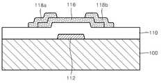
도 1은 본 발명의 실시예에 따른 산화물 반도체 박막 트랜지스터의 단면을 도시한 것이다.1 is a cross-sectional view of an oxide semiconductor thin film transistor according to an embodiment of the present invention.
도 1을 참조하면, 본 발명의 실시예에 따른 산화물 반도체 박막 트랜지스터는 채널층(116)과, 상기 채널층(116)의 일면 상에 순차적으로 형성되는 제1 게이트 절연막(110) 및 제1 게이트(112)와, 상기 채널층(116)의 타면 상에 순차적으로 형성되는 제2 게이트 절연막(120) 및 제2 게이트(122)를 포함한다. 여기서, 상기 제1 게이트 절연막(110)과 제2 게이트 절연막(120)은 서로 다른 물질로 이루어질 수 있다. 그리고, 상기 제1 게이트 절연막(110)과 제2 게이트 절연막(120)은 서로 다른 두께로 형성될 수 있다.1, an oxide semiconductor thin film transistor according to an embodiment of the present invention includes a
구체적으로, 기판(100) 상에는 제1 게이트(112) 및 제1 게이트 절연막(110)이 순차적으로 형성되어 있다. 상기 기판(100)으로는 투명 기판으로서 유리 기판이 일반적으로 사용되며, 이외에도 투명한 플라스틱 기판이 사용될 수도 있다. 상기 기판(100) 상에는 제1 게이트(112)가 형성되어 있다. 한편, 도 1에는 도시되어 있지 않으나, 상기 기판(100) 상에는 상기 제1 게이트(112)와 전기적으로 연결되어 상기 제1 게이트(112)에 소정 전압을 인가하는 게이트 라인(도 6의 211)이 형성될 수 있다. 상기 제1 게이트(112)는 기판(100) 상에 Mo 등과 같은 게이트 금속을 증착한 다음, 이를 패터닝함으로써 형성될 수 있다.Specifically, a
상기 기판(100) 상에는 상기 제1 게이트(112)를 덮도록 제1 게이트 절연막(110)이 형성되어 있다. 본 실시예에서, 상기 제1 게이트 절연막은(110) 후술하는 제2 게이트 절연막(120)과 다른 물질로 이루어질 수 있다. 구체적으로, 상기 제1 게이트 절연막(110)은 산소를 포함하지 않은 물질, 예를 들면, 실리콘 질화물로 이루어질 수 있다. 한편, 상기 제1 게이트 절연막(110)은 제2 게이트 절연막(120)과 다른 두께로 형성될 수 있다. 구체적으로, 상기 제1 게이트 절연막(110)의 두께(d1)는 제2 게이트 절연막(120)의 두께(d2)보다 두꺼울 수 있다. 예를 들면, 상기 제1 게이트 절연막(110)의 두께(d1)는 대략 2000Å ~ 1㎛ 정도가 될 수 있다. 하지만 이에 한정되는 것은 아니다.A first
상기 제1 게이트 절연막(110) 상에는 산화물 반도체로 이루어진 채널층(116)이 소정 두께로 형성되어 있다. 상기 채널층(116)은 상기 제1 게이트(112)의 상부에 위치한다. 상기 산화물 반도체는 예를 들면, Zinc Oxide, Tin Oxide, Ga-In-Zn Oxide, In-Zn Oxide, In-Sn Oxide 및 이들 물질에 Al, Ni, Cu, Ta, Mo, Hf 또는 Ti를 도핑한 물질 중 하나가 될 수 있다. 상기 채널층(116)은 대략 10nm ~ 300nm의 두께로 형성될 수 있다. 하지만, 이에 한정되는 것은 아니다. 상기 채널층(116)은 산화물 반도체를 제1 게이트 절연막(110) 상에 소정 두께로 증착한 다음, 이를 패터닝함으로써 형성될 수 있다. A
상기 산화물 반도체로 이루어진 채널층(116)의 상면 양측에는 각각 소스 전극(118a) 및 드레인 전극(118b)이 형성되어 있다. 상기 소스 전극(118a) 및 드레인 전극(118b)은 채널층(116)을 덮도록 제1 게이트 절연막(110) 상에 소정의 금속층을 형성한 다음, 이를 패터닝함으로써 형성될 수 있다. 여기서, 상기 금속층은 단일층 구조 또는 다층 구조를 가질 수 있다. 그리고, 상기 금속층은 예를 들면, Cu, Mo 및 Al 중 적어도 하나로 이루어질 수 있다. 한편, 도 1에 도시된 바와 달리 상기 소스 전극(118a) 및 드레인 전극(118b)은 채널층(116)의 양측 하면에 형성될 수도 있다. 상기 소스 전극(118a)은 데이터 라인(도 5의 219)과 전기적으로 연결될 수 있다.A
상기 채널층(116), 소스 전극(118a) 및 드레인 전극(118b)을 덮도록 상기 제1 게이트 절연막(110) 상에는 제2 게이트 절연막(120)이 소정 두께로 형성되어 있다. 본 실시예에서, 상기 제2 게이트 절연막(120)은 전술한 바와 같이 제1 게이트 절연막(110)과 다른 물질로 이루어질 수 있다. 구체적으로, 상기 제2 게이트 절연막(120)은 산소를 포함하는 물질, 예를 들면 실리콘 산화물로 이루어질 수 있다. 또한, 상기 제2 게이트 절연막(120)은 제1 게이트 절연막(110)과 다른 두께로 형성될 수 있다. 구체적으로, 상기 제2 게이트 절연막(120)의 두께(d2)는 제1 게이트 절연막(110)의 두께(d1)보다 얇게 형성될 수 있다. 예를 들면, 상기 제2 게이트 절연막(120)의 두께(d2)는 500Å ~ 5000Å 정도가 될 수 있다. 하지만 이에 한정되는 것은 아니다.A second
상기 제2 게이트 절연막(120) 상에는 제2 게이트(122)가 형성되어 있다. 상기 제2 게이트(122)는 채널층(116)의 상부에 위치하게 된다. 상기 제2 게이트(122) 는 제1 게이트(112)와 동일한 물질(예를 들면, Mo 등)로 이루어질 수 있다. 한편, 상기 제2 게이트(122)는 후술하는 바와 같이 화소 전극(도 8의 260)과 동일한 물질(예를 들면, ITO(Indium Tin Oxide) 또는 IZO(Indium Zinc Oxide)와 같은 투명한 도전성 물질)로 이루어질 수도 있다. 상기 제2 게이트(122)는 대략 0.08㎛ ~ 100㎛의 선폭을 가지고 형성될 수 있다. 하지만 이에 한정되는 것은 아니다.A
상기 제2 게이트(122)는 소정 전압이 인가됨에 따라 누설 전류를 억제하는 동시에 박막 트랜지스터의 턴 온(turn on) 상태에서의 작동 전류를 증대시키는 역할을 한다. 상기 제2 게이트(122)는 제1 게이트(112)와 전기적으로 연결되어 상기 제1 게이트(112)와 전기적으로 동기화될 수 있다. 이 경우, 상기 제2 게이트(122)는 상기 제2 게이트 절연막(120)과 제1 게이트 절연막(110)에 형성된 비아홀(도 7의 262)을 통하여 게이트 라인(도 6의 211)에 전기적으로 연결될 수 있다. 한편, 상기 제2 게이트(122)는 제1 게이트(112)와 전기적으로 연결되지 않은 독립된 라인(미도시)에 연결될 수도 있다. 상기 독립된 라인은 기판(100) 이나 다른 물질층 상에 형성될 수 있다. 이 경우, 상기 제2 게이트(122)에는 제1 게이트(112)와는 별도로 상기 독립된 라인을 통하여 소정의 직류 전압이 인가된다.The
상기와 같은 구조의 산화물 반도체 박막 트랜지스터에서, 상기 제2 게이트(122)에 소정 전압이 인가되면 채널층(116) 내의 상부를 통해 흐르는 누설전류를 억제할 수 있고, 문턱 전압(threshold voltage)를 종래 보다 양의 방향 쪽으로 이동시킬 수 있다. 그리고, 박막 트랜지스터가 턴 온(turn on)된 상태에서는 채널층(116) 내의 상부 및 하부 모두에서 전류의 이득이 있으므로, 문턱 전압 이전의 기울기(subthreshold slope) 또는 이동도(mobility)가 향상된다. 따라서, 동일한 구동전압에서 종래 보다 높은 작동 전류를 얻을 수 있다.In the oxide semiconductor thin film transistor having such a structure, when a predetermined voltage is applied to the
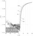
도 2는 하나의 게이트(single gate)를 구비한 산화물 반도체 박막 트랜지스터와 두 개의 게이트(double gate)를 구비한 산화물 반도체 박막 트랜지스터의 I-V 특성을 비교하여 도시한 것으로, 더블 게이트 구조의 산화물 반도체 박막 트랜지스터에서는 두 개의 게이트를 전기적으로 동기화시켰을 때 측정된 결과를 보여준다. 여기서, 채널층을 구성하는 산화물 반도체로는 Ga-In-Zn Oxide가 사용되었으며, 제1 게이트 절연막 및 제2 게이트 절연막은 각각 실리콘 질화물 및 실리콘 산화물로 형성하였다. 그리고, 상기 제1 게이트 절연막 및 제2 게이트 절연막은 각각 4000Å 및 2000Å 의 두께로 형성하였다. 채널층 하부의 제1 게이트 전극, 소스 및 드레인 전극은 Mo으로 형성하였으며, 채널층 상부의 제2 게이트 전극은 In-Zn Oxide으로 형성하였다.FIG. 2 is a graph comparing IV characteristics of an oxide semiconductor thin film transistor having a single gate and an oxide semiconductor thin film transistor having two gates. In the oxide semiconductor thin film transistor having a double gate structure, Shows the measured results when the two gates are electrically synchronized. Here, Ga-In-Zn oxide is used as an oxide semiconductor constituting the channel layer, and the first gate insulating film and the second gate insulating film are formed of silicon nitride and silicon oxide, respectively. The first gate insulating film and the second gate insulating film were formed to a thickness of 4000 Å and 2000 Å, respectively. The first gate electrode under the channel layer, the source and drain electrodes were formed of Mo, and the second gate electrode above the channel layer was formed of In-Zn oxide.
도 2를 참조하면, 두 개의 게이트(double gate)를 구비한 산화물 반도체 박막 트랜지스터에서는 문턱 전압이 하나의 게이트(single gate)를 구비한 산화물 박막 트랜지스터와 비교하여 양의 방향으로 대략 1.8V 정도 이동하였으며, 게이트 전압 0V에서의 전류는 1nA에서 1fA로 크게 감소하였다. 이는 제2 게이트 절연막 상에 형성된 제2 게이트에 의하여 채널층 내의 상부를 통해 흐르는 누설 전류가 억제되었기 때문이다. 그리고, 싱글 게이트 및 더블 게이트 구조의 박막 트랜지스터에서, 이동도(mobility)는 각각 9.1cm2/Vs 및 32.1cm2/Vs이었다. 따라서, 더블 게이트 구 조의 박막 트랜지스터는 이동도가 대략 3.5배 정도 증가하였음을 알 수 있다. 이는 제2 게이트 절연막 상에 형성된 제2 게이트에 의한 영향 뿐만아니라 제1 게이트 절연막 보다 얇은 두께로 형성된 제2 게이트 절연막의 영향에 기인하는 것으로 해석될 수 있다. 또한, 문턱 전압 이전의 기울기(subthreshold slope)는 각각 1.45 dec/V 및 1.85 dec/V 이었다. 따라서, 더블 게이트 구조의 박막 트랜지스터는 싱글 게이트 구조의 박막 트랜지스터보다 문턱 전압 이전의 기울기(subthreshold slope)가 대략 1.27배 정도 증가하였음을 알 수 있다.Referring to FIG. 2, in an oxide semiconductor thin film transistor having two gates, the threshold voltage is shifted by about 1.8 V in the positive direction as compared with the oxide thin film transistor having a single gate , The current at the gate voltage of 0 V was greatly reduced from 1 nA to 1 fA. This is because the leakage current flowing through the upper portion in the channel layer by the second gate formed on the second gate insulating film is suppressed. Then, in the transistor of the single-gate and double-gate structure, the mobility (mobility) was each 9.1cm2 / Vs and 32.1cm2 / Vs. Therefore, it can be seen that the mobility of the thin film transistor of the double gate structure is increased by about 3.5 times. This can be interpreted as not only the effect of the second gate formed on the second gate insulating film but also the influence of the second gate insulating film formed to be thinner than the first gate insulating film. In addition, the subthreshold slope before the threshold voltage was 1.45 decV and 1.85 decV, respectively. Therefore, it can be seen that the subthreshold slope of the double-gate thin film transistor is about 1.27 times larger than that of the single gate thin film transistor.
도 3은 하나의 게이트를 구비한 산화물 반도체 박막 트랜지스터와 두 개의 게이트를 구비한 산화물 반도체 박막 트랜지스터의 I-V 특성을 비교하여 도시한 것으로, 더블 게이트 구조의 산화물 반도체 박막 트랜지스터에서는 제2 게이트를 독립된 라인에 연결시켰을 때 측정된 결과를 보여준다. 도 4에서 V1 및 V2는 각각 제1 및 제2 게이트에 인가되는 전압을 나타낸다. 여기서, 채널층을 구성하는 산화물 반도체로는 Ga-In-Zn Oxide가 사용되었으며, 게이트절연막 및 제2 게이트 절연막은 각각 실리콘 질화물 및 실리콘 산화물로 형성하였다. 그리고, 상기 제1 게이트 절연막 및 제2 게이트 절연막은 각각 4000Å 및 2000Å 의 두께로 형성하였다. 채널층 하부의 제1 게이트, 소스 및 드레인 전극은 Mo으로 형성하였으며, 채널층 상부의 제2 게이트는 In-Zn Oxide으로 형성하였다.FIG. 3 illustrates IV characteristics of an oxide semiconductor thin film transistor having one gate and an oxide semiconductor thin film transistor having two gates. In the oxide semiconductor thin film transistor having a double gate structure, the second gate is connected to an independent line It shows the measured result when connected. 4, V1 and V2 represent voltages applied to the first and second gates, respectively. Here, Ga-In-Zn oxide was used as an oxide semiconductor constituting the channel layer, and the gate insulating film and the second gate insulating film were formed of silicon nitride and silicon oxide, respectively. The first gate insulating film and the second gate insulating film were formed to a thickness of 4000 Å and 2000 Å, respectively. The first gate, source and drain electrodes under the channel layer were formed of Mo, and the second gate over the channel layer was formed of In-Zn oxide.
도 3을 참조하면, 제2 게이트 전압(V2)이 -10V인 경우에는 제1 게이트 전압(V1)이 -20V ~ 20V의 범위 내에서 박막 트랜지스터는 항상 턴 오프된 상태이다. 그러나, 제2 게이트 전압(V2)이 +10V인 경우에는 문턱 전압이 싱글 게이트 구조보다 음의 방향 쪽으로 이동하고, 작동 전류를 증가한다. 그리고, 제2 게이트 전압(V2)이 0V인 경우에는 문턱 전압이 싱글 게이트 구조보다 양의 방향으로 대략 7V 정도 이동하였다. 이와 같이, 본 발명의 실시예에 따른 산화물 반도체 박막 트랜지스터에서는 I-V 특성이 제1 게이트보다 오히려 제2 게이트에 의존하는 특성을 보여준다. 이는 본 실험에서 제작된 본 발명의 실시예에 따른 박막 트랜지스터는 산화물 반도체로 이루어진 채널층이 대략 700Å 정도로 얇은 두께로 형성되었기 때문에 제1 및 제2 게이트에 의하여 형성된 전계가 채널층 내의 상부 및 하부 모두에 영향을 줄 수 있는 구조이기 때문으로 보인다. 그리고, 제1 게이트 절연막이 4000Å 두께의 실리콘 질화막으로 형성되고 제2 게이트 절연막은 2000Å 두께의 실리콘 산화막으로 형성됨으로써 제2 게이트 절연막의 캐퍼시턴스가 제1 게이트 절연막의 캐퍼시터스 보다 컸기 때문에 제2 게이트의 영향이 크게 관찰된 것으로 보인다. 따라서, 제2 게이트 절연막의 두께 및 유전 상수를 조절하게 되면 제2 게이트의 영향을 변화시킬 수 있음을 알 수 있다. 구체적으로, 제2 게이트 절연막의 캐퍼시턴스가 제1 게이트 절연막의 캐퍼시턴스 보다 클수록 제2 게이트의 영향이 커지게 된다. 또한, 채널층의 두께가 얇을수록 제2 게이트의 영향이 커지게 되고, 제2 게이트의 선폭이 증가할수록 제2 게이트의 영향이 커지게 된다. 이로부터, 더블 게이트 구조의 산화물 반도체 박막 트랜지스터에서는 제2 게이트에 인가되는 전압, 채널층의 두께, 제2 게이트 절연막의 두께와 유전상수 및 제2 게이트의 선폭 중 적어도 하나를 조절 하게 되면, 제2 게이트의 영향을 변화시킬 수 있고, 이에 따라 문턱 전압이 제어될 수 있음을 알 수 있다. 더블 게이트 구조의 산화물 반도체 박막 트랜지스터에서는 소스-드레인 전극 패터닝 공정과, 포토레지스트 제거공정(Ashing), 제2 게이트 절연막 증착 공정 중에 산화물 반도체의 백 채널(Back Channel)영역이 플라즈마 손상을 받게 되므로 누설 전류는 증가하고, 플라즈마 손상에 의한 trap site의 증가로 바이어스 인가시 문턱 전압의 변화량이 증가하게 된다. 따라서, 누설전류와 Charge Trapping을 억제하기 위해 제2 게이트의 전기장(Electric Field)을 조절할 수 있다. 제2 게이트의 전기장 조절을 통한 누설전류 감소와 신뢰성 향상은 제2 게이트 절연막의 두께를 감소시키고 제2게이트에 제1게이트와 동등한 전압을 인가함으로써 실현 될 수 있다.Referring to FIG. 3, when the second gate voltage V2 is -10 V, the thin film transistor is always turned off within the range of -20 V to 20 V of the first gate voltage V1 . However, when the second gate voltage V2 is + 10V, the threshold voltage shifts toward the negative direction and increases the operating current. When the second gate voltage V2 is 0 V, the threshold voltage is shifted by about 7 V in the positive direction from the single gate structure. Thus, in the oxide semiconductor thin film transistor according to the embodiment of the present invention, the IV characteristic depends on the second gate rather than the first gate. In this case, since the channel layer made of the oxide semiconductor is formed to have a thickness as thin as about 700 ANGSTROM, the electric field formed by the first and second gates is formed in both the upper and lower parts of the channel layer This is because it is a structure that can influence the influence of Since the first gate insulating film is formed of a silicon nitride film having a thickness of 4000A and the second gate insulating film is formed of a silicon oxide film having a thickness of 2000A, the capacitance of the second gate insulating film is larger than the capacitance of the first gate insulating film. And the effect of Therefore, it can be seen that the influence of the second gate can be changed by adjusting the thickness and the dielectric constant of the second gate insulating film. Specifically, as the capacitance of the second gate insulating film is larger than the capacitance of the first gate insulating film, the influence of the second gate becomes larger. Also, the thinner the channel layer, the larger the effect of the second gate, and the larger the line width of the second gate, the greater the influence of the second gate. Thus, in the oxide semiconductor thin film transistor having the double gate structure, if at least one of the voltage applied to the second gate, the thickness of the channel layer, the thickness and the dielectric constant of the second gate insulating film, and the line width of the second gate is controlled, It can be seen that the influence of the gate can be changed and thus the threshold voltage can be controlled. In the oxide semiconductor thin film transistor having the double gate structure, since the back channel region of the oxide semiconductor is subjected to plasma damage during the patterning process of the source-drain electrode, the photoresist removing process (ashing) and the second gate insulating film deposition process, And the variation of the threshold voltage is increased when the bias is applied due to the increase of the trap site due to the plasma damage. Therefore, the electric field of the second gate can be adjusted to suppress leakage current and charge trapping. The leakage current reduction and reliability improvement through the adjustment of the electric field of the second gate can be realized by reducing the thickness of the second gate insulating film and applying a voltage equal to the first gate to the second gate.
도 4a 및 도 4b는 하나의 게이트(single gate)를 구비한 산화물 반도체 박막 트랜지스터의 바이어스 인가 시간에 따른 I-V 특성을 도시한 것이다. 구체적으로, 도 4a는 60℃에서 게이트와 소스 전극 사이에 네가티브 바이어스 전압(DC -20V)를 인가하고, 그 인가 시간에 따라 I-V 특성을 도시한 것이다. 그리고, 도 4b는 60℃에서 게이트와 소스 전극 사이에 포지티브 바이어스 전압(DC +20V)를 인가하고, 그 인가 시간에 따라 I-V 특성을 도시한 것이다. 여기서, 채널층을 구성하는 산화물 반도체로는 Ga-In-Zn Oxide가 사용되었다. 그리고, 제1 게이트절연막 및 제2 게이트 절연막은 각각 실리콘 질화물 및 실리콘 산화물로 형성하였으며, 게이트, 소스 및 드레인 전극은 Mo으로 형성하였다.FIGS. 4A and 4B illustrate I-V characteristics according to a bias application time of an oxide semiconductor thin film transistor having a single gate. Specifically, FIG. 4A shows the I-V characteristic according to the application time of a negative bias voltage (DC-20V) between the gate and the source electrode at 60 ° C. 4B shows the I-V characteristic according to the application time of the positive bias voltage (DC + 20V) between the gate and the source electrode at 60 ° C. Here, Ga-In-Zn Oxide is used as an oxide semiconductor constituting the channel layer. The first gate insulating film and the second gate insulating film were formed of silicon nitride and silicon oxide, respectively, and the gate, source and drain electrodes were formed of Mo.
도 4a 및 도 4b를 참조하면, 종래 싱글 게이트 구조의 산화물 반도체 박막 트랜지스터에서는, 네가티브 바이어스 전압이 3시간 동안 인가된 후에 문턱 전압이 대략 -9.7V 정도 변화되었으며, 포지티브 바이어스 전압이 3시간 동안 인가된 후에 문턱 전압이 대략 +6.6V 정도 변화되었다.4A and 4B, in the oxide semiconductor thin film transistor of the conventional single gate structure, after a negative bias voltage is applied for 3 hours, a threshold voltage is changed by about -9.7 V, and when a positive bias voltage is applied for 3 hours The threshold voltage was changed by about +6.6 V later.
도 5a 및 도 5b는 두 개의 제1 및 제2 게이트(double gate)를 구비한 산화물 반도체 박막 트랜지스터의 바이어스 인가 시간에 따른 I-V 특성을 도시한 것이다. 여기서, 상기 제1 게이트는 제2 게이트와 동기화되도록 제2 게이트에 전기적으로 연결되어 있다. 구체적으로, 도 5a는 60℃에서 제1 및 제2 게이트와 소스 전극 사이에 네가티브 바이어스 전압(DC -20V)를 인가하고, 그 인가 시간에 따라 I-V 특성을 도시한 것이다. 그리고, 도 5b는 60℃에서 제1 및 제2 게이트와 소스 전극 사이에 포지티브 바이어스 전압(DC +20V)를 인가하고, 그 인가 시간에 따라 I-V 특성을 도시한 것이다. 여기서, 산화물 반도체로는 Ga-In-Zn Oxide가 사용되었으며, 게이트절연막 및 제2 게이트 절연막은 각각 실리콘 질화물 및 실리콘 산화물로 형성하였다. 그리고, 상기 제1 게이트 절연막 및 제2 게이트 절연막은 각각 4000Å 및 2000Å 의 두께로 형성하였다. 채널층 하부의 제1 게이트, 소스 및 드레인 전극은 Mo으로 형성하였으며, 채널층 상부의 제2 게이트는 In-Zn Oxide으로 형성하였다.FIGS. 5A and 5B show I-V characteristics according to a bias application time of an oxide semiconductor thin film transistor having two first and second gates. Here, the first gate is electrically connected to the second gate so as to be synchronized with the second gate. Specifically, FIG. 5A shows the I-V characteristic according to the application time of a negative bias voltage (DC-20V) between the first and second gates and the source electrode at 60 ° C. 5B shows the I-V characteristic according to the application time of the positive bias voltage (DC + 20V) between the first and second gates and the source electrode at 60 ° C. Here, Ga-In-Zn oxide was used as the oxide semiconductor, and the gate insulating film and the second gate insulating film were formed of silicon nitride and silicon oxide, respectively. The first gate insulating film and the second gate insulating film were formed to a thickness of 4000 Å and 2000 Å, respectively. The first gate, source and drain electrodes under the channel layer were formed of Mo, and the second gate over the channel layer was formed of In-Zn oxide.
도 5a 및 도 5b를 참조하면, 더블 게이트 구조의 산화물 반도체 박막 트랜지스터에서는, 네가티브 바이어스 전압이 예를 들어 3시간 동안 인가된 후에 문턱 전압이 대략 +0.2V 정도 변화되었으며, 포지티브 바이어스 전압이 예를 들어 3시간 동안 인가된 후에 문턱 전압은 대략 +2.7V 정도 변화되었다.5A and 5B, in the oxide semiconductor thin film transistor having the double gate structure, the threshold voltage is changed by about +0.2 V after the application of the negative bias voltage for, for example, 3 hours, and the positive bias voltage is, for example, After the application for 3 hours, the threshold voltage was changed by about + 2.7V.
이와 같이, 더블 게이트 구조의 산화물 반도체 박막 트랜지스터에서는 싱글 게이트 구조의 산화물 반도체 박막 트랜지스터와 비교하여, 네가티브 바이어스가 인가된 경우에는 문턱 전압 변화량이 9.7V에서 0.2V로 크게 줄어들었으며, 포지티브 바이어스가 인가된 경우에도 문턱 전압 변화량이 6.6V에서 2.7V로 크게 줄어들었음을 알 수 있다. 따라서, 더블 게이트 구조의 산화물 반도체 박막 트랜지스터는 싱글 게이트 구조의 산화물 반도체 박막 트랜지스터 보다 전기적인 신뢰성이 향상될 수 있음을 알 수 있다. 더블 게이트 구조의 산화물 반도체 박막 트랜지스터에서, 이러한 전기적인 신뢰성 향상은 첫째로는 제1 및 제2 게이트 동시에 전압이 인가됨으로써 활성층 내에 캐리어가 분산되고, 또한 제1 게이트에 의한 전계(field)와 제2 게이트에 의한 전계가 중첩됨으로써 전체 전계(total field)가 약화되었다는데 그 원인이 있을 수 있으며, 둘째로는 제2 게이트 절연막을 이루는 실리콘 산화물은 문턱 전압을 양의 방향으로 이동시킬 수 있는 반면에 제1 게이트 절연막을 이루는 실리콘 질화물은 문턱 전압을 음의 방향으로 이동시킬 수 있다는데 그 원인이 있을 수 있다.As described above, in the oxide semiconductor thin film transistor having the double gate structure, when the negative bias is applied, the amount of change in the threshold voltage is greatly reduced from 9.7 V to 0.2 V as compared with the oxide semiconductor thin film transistor having the single gate structure. It can be seen that the threshold voltage variation is greatly reduced from 6.6V to 2.7V. Therefore, it can be seen that the oxide semiconductor thin film transistor having the double gate structure can be more improved in electric reliability than the oxide semiconductor thin film transistor having the single gate structure. In the oxide semiconductor thin film transistor of the double gate structure, such electrical reliability improvement is achieved by firstly distributing the carriers in the active layer by applying the first and second gate voltages simultaneously, Second, the silicon oxide forming the second gate insulating film can shift the threshold voltage in the positive direction, whereas the silicon oxide forming the second gate insulating film can shift the threshold voltage in the positive direction. On the other hand, The silicon nitride forming one gate insulating film can cause the threshold voltage to move in the negative direction.
이상에서 설명된 본 발명의 실시예에 따른 산화물 반도체 박막 트랜지스터는 디스플레이 장치의 구동 회로부 뿐만 아니라 화소부에도 적용될 수 있다.The oxide semiconductor thin film transistor according to the embodiment of the present invention described above can be applied to a pixel portion as well as a driving circuit portion of a display device.
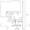
도 6은 디스플레이 장치의 화소부에 적용된 본 발명의 다른 실시예에 따른 산화물 반도체 박막 트랜지스터의 평면을 도시한 것이다. 그리고, 도 7은 도 6의 Ⅵ-Ⅵ'선을 따라 본 단면도이며, 도 8은 도 6의 Ⅶ-Ⅶ'선을 따라 본 단면도이다. 이하에서는 전술한 실시예와 다른 점을 중심으로 설명하기로 한다.6 is a plan view of an oxide semiconductor thin film transistor according to another embodiment of the present invention applied to a pixel portion of a display device. 7 is a cross-sectional view taken along a line VI-VI 'of FIG. 6, and FIG. 8 is a cross-sectional view taken along line VII-VII' of FIG. Hereinafter, differences from the above-described embodiment will be mainly described.
도 6 내지 도 8을 참조하면, 기판(200) 상에 제1 게이트(212) 및 게이트 라 인(211)이 형성되어 있다. 상기 게이트 라인(211)은 상기 제1 게이트(212)에 전기적으로 연결되어 상기 제1 게이트(212)에 소정 전압을 인가한다. 그리고, 상기 기판(200) 상에는 제1 게이트(212) 및 게이트 라인(212)을 덮도록 제1 게이트 절연막(210)이 형성되어 있다. 여기서, 상기 제1 게이트 절연막(210)은 산소를 포함하지 않은 물질, 예를 들면, 실리콘 질화물로 이루어질 수 있다. 한편, 상기 제1 게이트 절연막(210)은 제2 게이트 절연막(220)과 다른 두께로 형성될 수 있다. 구체적으로, 상기 제1 게이트 절연막(210)의 두께(d1)는 제2 게이트 절연막(220)의 두께(d2)보다 두꺼울 수 있다.Referring to FIGS. 6 to 8, a
상기 제1 게이트(212)의 상부에 위치하는 제1 게이트 절연막(210) 상에는 산화물 반도체로 이루어진 채널층(216)이 소정 두께로 형성되어 있다. 상기 산화물 반도체는 예를 들면, Zinc Oxide, Tin Oxide, Ga-In-Zn Oxide, In-Zn Oxide, In-Sn Oxide 및 이들 물질에 Al, Ni, Cu, Ta, Mo, Hf 또는 Ti를 도핑한 물질 중 하나가 될 수 있다. 그리고, 상기 채널층(216)은 대략 10nm ~ 300nm의 두께로 형성될 수 있다.A
상기 산화물 반도체로 이루어진 채널층(216)의 상면 양측에는 각각 소스 전극(218a) 및 드레인 전극(218b)이 형성되어 있다. 한편, 상기 소스 전극(218a)은 데이터 라인(219)과 전기적으로 연결되어 있다. 상기 채널층(216), 소스 전극(218a) 및 드레인 전극(218b)을 덮도록 상기 제1 게이트 절연막(210) 상에는 제2 게이트 절연막(220)이 소정 두께로 형성되어 있다. 여기서, 상기 제2 게이트 절연 막(220)은 산소를 포함하는 물질, 예를 들면 실리콘 산화물로 이루어질 수 있다. 또한, 상기 제2 게이트 절연막(220)은 제1 게이트 절연막(210)과 다른 두께로 형성될 수 있다. 구체적으로, 상기 제2 게이트 절연막(120)의 두께(d2)는 제1 게이트 절연막(110)의 두께(d1)보다 얇게 형성될 수 있다.A
상기 제2 게이트 절연막(220) 상에는 제2 게이트(222)가 형성되어 있다. 상기 제2 게이트(222)는 채널층(216)의 상부에 위치하게 된다. 상기 제2 게이트(222)는 대략 0.08㎛ ~ 100㎛의 선폭을 가지고 형성될 수 있다. 여기서, 상기 제2 게이트(222)는 전술한 바와 같이 소정 전압이 인가됨에 따라 누설 전류를 억제하는 동시에 박막 트랜지스터의 턴 온(turn on) 상태에서의 작동 전류를 증대시키는 역할을 한다.A
상기 제2 게이트 절연막(220) 상에는 화소 전극(250)이 드레인 전극(218b)과 전기적으로 연결되도록 형성되어 있다. 이를 위하여, 도 7에 도시된 바와 같이 상기 드레인 전극(218b)의 상부에 형성된 제2 게이트 절연막(220)에는 상기 드레인 전극(218b)을 노출시키는 제1 비아홀(261)이 형성되어 있으며, 상기 제1 비아홀(216)을 통하여 상기 화소전극(250)은 드레인 전극(218b)과 연결되도록 형성되어 있다. 상기 화소 전극(250)은 예를 들면, ITO(Indium Tin Oxide) 또는 IZO(Indium Zinc Oxide)와 같은 투명한 도전성 물질로 이루어질 수 있다. 한편, 상기 화소 전극(250)은 상기 제2 게이트 절연막(220) 상에 제2 게이트(222)와 동시에 형성될 수 있다. 이 경우, 상기 제2 게이트(222)는 상기 화소 전극(250)을 이루는 물질과 동 일한 물질로 이루어질 수 있다.The
상기 제2 게이트(222)는 도 8에 도시된 바와 같이 게이트 라인(211)에 전기적으로 연결되도록 형성되어 있다. 이를 위하여, 상기 게이트 라인(211)의 상부에 형성된 제1 게이트 절연막(210) 및 제2 게이트 절연막(220)에는 게이트 라인(211)을 노출시키는 제2 비아홀(262)이 형성되어 있으며, 상기 제2 비아홀(262)을 통하여 상기 제2 게이트(222)가 게이트 라인(211)과 연결되도록 형성되어 있다. 이에 따라, 상기 제2 게이트(222)는 제1 게이트(212)와 전기적으로 연결되어 상기 제1 게이트(212)와 전기적으로 동기화될 수 있다.The
한편, 이상에서는 상기 제2 게이트(222)가 제1 게이트(212)와 전기적으로 연결되는 경우가 설명되었으나, 상기 제2 게이트(222)는 제1 게이트(212)와 전기적으로 연결되지 않은 독립된 라인(미도시)에 연결될 수도 있다. 여기서, 상기 독립된 라인은 기판(200) 이나 다른 물질층 상에 형성될 수 있다. 이 경우, 상기 제2 게이트(222)에는 제1 게이트(212)와는 별도로 상기 독립된 라인을 통하여 소정의 직류 전압이 인가된다.Although the
이하에서는 본 발명의 실시예에 따른 산화물 반도체 박막 트랜지스터의 제조방법에 대하여 설명한다. 도 9 내지 도 11은 상술한 더블 게이트 구조의 산화물 반도체 박막 트랜지스터의 제조방법을 설명하기 위한 도면들이다.Hereinafter, a method of manufacturing an oxide semiconductor thin film transistor according to an embodiment of the present invention will be described. 9 to 11 are views for explaining a method of manufacturing the oxide semiconductor thin film transistor having the double gate structure described above.
도 9를 참조하면, 먼저 기판(100) 상에 제1 게이트(112)를 형성한다. 여기서, 상기 제1 게이트(112)는 기판(100) 상에 소정의 게이트 금속을 증착한 다음, 이를 패터닝함으로써 형성될 수 있다. 그리고, 이 과정에서 상기 제1 게이트(212) 와 전기적으로 연결되는 게이트 라인(도 6의 211)이 기판(100) 상에 같이 형성될 수 있다. 다음으로, 기판(100) 상에 상기 제1 게이트(112)를 덮도록 제1 게이트 절연막(110)을 형성한다. 여기서, 상기 제1 게이트 절연막은(110) 산소를 포함하지 않은 물질, 예를 들면, 실리콘 질화물로 이루어질 수 있다. 그리고, 상기 제1 게이트 절연막(110)은 후술하는 제2 게이트 절연막(120)보다 두꺼운 두께로 형성될 수 있다. 구체적으로 예를 들면, 상기 제1 게이트 절연막(110)의 두께(d1)는 대략 2000Å ~ 1㎛ 정도가 될 수 있다. 하지만 이에 한정되는 것은 아니다.Referring to FIG. 9, a
도 10을 참조하면, 상기 제1 게이트 절연막(110) 상에 산화물 반도체로 이루어진 채널층(216)을 형성한다. 여기서, 상기 채널층(116)은 상기 제1 게이트(112)의 상부에 위치하도록 형성된다. 상기 채널층(116)은 산화물 반도체를 제1 게이트 절연막(110) 상에 소정 두께로 증착한 다음, 이를 패터닝함으로써 형성될 수 있다. 상기 산화물 반도체는 예를 들면, Zinc Oxide, Tin Oxide, Ga-In-Zn Oxide, In-Zn Oxide, In-Sn Oxide 및 이들 물질에 Al, Ni, Cu, Ta, Mo, Hf 또는 Ti를 도핑한 물질 중 하나가 될 수 있다. 그리고, 상기 채널층(116)은 대략 10nm ~ 300nm의 두께로 형성될 수 있다. 하지만, 이에 한정되는 것은 아니다. 이어서, 상기 산화물 반도체로 이루어진 채널층(116)의 상면 양측에 각각 소스 전극(118a) 및 드레인 전극(118b)을 형성한다. 상기 소스 전극(118a) 및 드레인 전극(118b)은 채널층(116)을 덮도록 제1 게이트 절연막(110) 상에 소정의 금속층을 형성한 다음, 이를 패터닝함으로써 형성될 수 있다. 여기서, 상기 금속층은 단일층 구조 또는 다층 구조를 가질 수 있다. 그리고, 상기 금속층은 예를 들면, Cu, Mo 및 Al 중 적어도 하나로 이루어질 수 있다. 한편, 상기 소스 전극(118a) 및 드레인 전극(118b)을 형성한 다음, 상기 소스 전극(118a)과 드레인 전극(118b) 사이에 있는 채널층(116) 내의 상부에 산소를 공급하기 위하여 도 10에 도시된 구조물에 산소 이온을 포함하는 플라즈마 처리 공정을 수행하는 단계가 더 포함될 수도 있다. 한편, 이상에서는 채널층(116)을 형성한 다음, 상기 채널층(116)의 상면 양측에 소스 전극(118a) 및 드레인 전극(118b)을 형성하는 경우가 설명되었으나, 상기 소스 전극(118a) 및 드레인 전극(118b)을 먼저 형성한 다음, 이 소스 전극(118a)과 드레인 전극(118b) 상에 채널층(116)을 형성할 수도 있다.Referring to FIG. 10, a
도 11을 참조하면, 상기 채널층(116), 소스 전극(118a) 및 드레인 전극(118b)을 덮도록 상기 제1 게이트 절연막(110) 상에 제2 게이트 절연막(120)을 형성한다. 여기서, , 상기 제2 게이트 절연막(120)은 전술한 제1 게이트 절연막(110)과 다른 물질로 이루어질 수 있다. 구체적으로, 상기 제2 게이트 절연막(120)은 산소를 포함하는 물질, 예를 들면 실리콘 산화물로 이루어질 수 있다. 또한, 상기 제2 게이트 절연막(120)은 제1 게이트 절연막(110)보다 얇은 두께로 형성될 수 있다. 구체적으로, 상기 제2 게이트 절연막(120)의 두께(d2)는 500Å ~ 5000Å 정도가 될 수 있다. 하지만 이에 한정되는 것은 아니다.Referring to FIG. 11, a second
이어서, 상기 채널층(116)의 상부에 위치하는 제2 게이트 절연막(120) 상에 제2 게이트(122)를 형성한다. 상기 제2 게이트(122)는 제2 게이트 절연막(120) 상 에 소정의 게이트 금속을 증착한 다음, 이를 패터닝함으로써 형성될 수 있다. 여기서, 상기 제2 게이트(122)는 대략 0.08㎛ ~ 100㎛의 선폭을 가지고 형성될 수 있다.Next, a
도면에는 도시되어 있지 않으나 상기 제2 게이트(122)를 게이트 라인에 연결되도록 형성하는 경우에는 먼저, 게이트 라인의 상부에 위치하는 제1 게이트 절연막(110) 및 제2 게이트 절연막(120)을 식각하여 게이트 라인을 노출시키는 비아홀을 형성한 다음, 상기 비아홀의 내벽 및 제2 게이트 절연막(120) 상에 상기 제2 게이트(122)를 형성할 수 있다. 한편, 상기 제2 게이트(122)를 제1 게이트(112)와 연결되지 않은 독립된 라인에 연결되도록 형성하는 경우에는, 상기 독립된 라인의 상부에 형성된 물질층에 노출시키는 비아홀을 형성 다음, 상기 비아홀의 내벽 및 제2 게이트 절연막(120) 상에 상기 제2 게이트(122)를 형성할 수 있다. 여기서, 상기 독립된 라인은 기판(100)이나 다른 물질층 상에 형성될 수 있다.Although not shown in the figure, when the
한편, 상기 제2 게이트 절연막(120) 상에 화소 전극을 더 형성하는 경우에는 상기 화소 전극은 제2 게이트(122)와 동시에 형성될 수 있다. 구체적으로, 먼저 드레인 전극(118b)의 상부에 위치한 제2 게이트 절연막(120)에 드레인 전극(118b)을 노출시키는 비아홀을 형성한다. 그리고, 상기 제2 게이트 절연막(120) 및 비아홀을 덮도록 소정 물질을 증착한 다음, 이를 패터닝하여 제2 게이트(122) 및 화소 전극을 형성한다. 이에 따라, 상기 제2 게이트(122)는 채널층(116)의 상부에 위치한 제2 게이트 절연막(120) 상에 형성되며, 상기 화소 전극은 비아홀의 내벽 및 제2 게이트 절연막(120) 상에 형성될 수 있다. 여기서, 상기 제2 게이트(122) 및 화소전 극은 예를 들면, ITO(Indium Tin Oxide) 또는 IZO(Indium Zinc Oxide)와 같은 투명한 도전성 물질로 이루어질 수 있다.Meanwhile, when a pixel electrode is further formed on the second
한편, 이상의 실시예들에서는 Bottom Gate BCE(Back Channel Etch) 구조의 박막 트랜지스터가 설명되었다. 그러나, 이는 예시적인 것에 불과하며 본 발명의 기술적 사상은 다른 구조의 박막 트랜지스터 예를 들면 Bottom Gate Etch Stop 구조 또는 Top Gate 구조의 박막 트랜지스터에도 얼마든지 적용가능하다. 구체적으로, 상기 Bottom Gate Etch Stop 구조의 박막 트랜지스터에서는 소스 전극과 드레인 전극 사이의 채널층 상면에 식각 정지층(etch stop layer)가 형성되며, 상기 Top Gate 구조의 박막 트랜지스터에서는 채널층을 기준으로 채널층의 상부 쪽에 제1 게이트 및 제1 게이트 절연막이 위치하게 되고, 채널층의 하부 쪽에 제2 게이트 및 제2 게이트 절연막이 위치하게 된다.In the above embodiments, a thin film transistor having a bottom gate BCE (Back Channel Etch) structure has been described. However, this is merely an example, and the technical idea of the present invention is applicable to thin film transistors of other structures, for example, a bottom gate etch stop structure or a top gate structure. Specifically, in the TFT having the bottom gate etch stop structure, an etch stop layer is formed on the channel layer between the source electrode and the drain electrode. In the TFT having the top gate structure, The first gate and the first gate insulating film are located on the upper side of the layer, and the second gate and the second gate insulating film are located on the lower side of the channel layer.
이상에서 본 발명의 실시예들이 설명되었으나, 이는 예시적인 것에 불과하며, 당해 분야에서 통상적 지식을 가진 자라면 이로부터 다양한 변형 및 균등한 타 실시예가 가능하다는 점을 이해할 것이다.While the invention has been shown and described with reference to certain preferred embodiments thereof, it will be understood by those skilled in the art that various changes and modifications may be made without departing from the scope of the invention as defined by the appended claims.
도 1은 본 발명의 실시예에 따른 산화물 반도체 박막 트랜지스터의 단면을 도시한 것이다.1 is a cross-sectional view of an oxide semiconductor thin film transistor according to an embodiment of the present invention.
도 2는 더블 게이트 구조의 산화물 반도체 박막 트랜지스터에서, 제1 게이트와 제2 게이트를 동기화시켰을 때 I-V 특성을 도시한 것이다.2 shows the I-V characteristic when the first gate and the second gate are synchronized in the oxide semiconductor thin film transistor of the double gate structure.
도 3은 더블 게이트 구조의 산화물 반도체 박막 트랜지스터에서, 제2 게이트를 독립된 라인에 연결시켰을 때 I-V 특성을 도시한 것이다.3 shows the I-V characteristic when the second gate is connected to an independent line in the oxide semiconductor thin film transistor of the double gate structure.
도 4a 및 도 4b는 싱글 게이트 구조의 산화물 반도체 박막 트랜지스터의 바이어스 인가 시간에 따른 I-V 특성을 도시한 것이다.4A and 4B illustrate I-V characteristics of the oxide semiconductor thin film transistor having a single gate structure according to a bias application time.
도 5a 및 도 5b는 더블 게이트 구조의 산화물 반도체 박막 트랜지스터의 바이어스 인가 시간에 따른 I-V 특성를 도시한 것이다.FIGS. 5A and 5B show I-V characteristics of the oxide semiconductor thin film transistor having a double gate structure according to bias application time. FIG.
도 6은 디스플레이 장치의 화소부에 적용된 본 발명의 다른 실시예에 따른 산화물 반도체 박막 트랜지스터의 평면을 도시한 것이다.6 is a plan view of an oxide semiconductor thin film transistor according to another embodiment of the present invention applied to a pixel portion of a display device.
도 7은 도 6의 Ⅵ-Ⅵ'선을 따라 본 단면도이다.7 is a cross-sectional view taken along line VI-VI 'of FIG.
도 8은 도 6의 Ⅶ-Ⅶ'선을 따라 본 단면도이다.8 is a cross-sectional view taken along line VII-VII 'of FIG.
도 9 내지 도 11은 본 발명의 또 다른 실시예에 따른 산화물 반도체 박막 트랜지스터의 제조방법을 설명하기 위한 도면들이다.9 to 11 are views for explaining a method of manufacturing an oxide semiconductor thin film transistor according to still another embodiment of the present invention.
<도면의 주요 부분에 대한 부호의 설명>Description of the Related Art
100,200... 기판 110,210... 제1 게이트 절연막100, 200 ...
112,212... 제1 게이트 116,216... 채널층112, 112 ...
118a.218a... 소스 전극 118b,218b... 드레인 전극
120,220... 제2 게이트 절연막 122,222... 제2 게이트120, 220 ... second
211... 게이트 라인 219... 데이터 라인211 ...
250... 화소 전극 261... 제1 비아홀250 ...
262... 제2 비아홀262 ... second via hole
Claims (35)
Translated fromKoreanPriority Applications (2)
| Application Number | Priority Date | Filing Date | Title |
|---|---|---|---|
| EP09151196.4AEP2086013B1 (en) | 2008-02-01 | 2009-01-23 | Oxide semiconductor transistor |
| US12/320,701US8586979B2 (en) | 2008-02-01 | 2009-02-02 | Oxide semiconductor transistor and method of manufacturing the same |
Applications Claiming Priority (2)
| Application Number | Priority Date | Filing Date | Title |
|---|---|---|---|
| KR20080010816 | 2008-02-01 | ||
| KR1020080010816 | 2008-02-01 |
Publications (2)
| Publication Number | Publication Date |
|---|---|
| KR20090084642A KR20090084642A (en) | 2009-08-05 |
| KR101512818B1true KR101512818B1 (en) | 2015-05-20 |
Family
ID=41205151
Family Applications (1)
| Application Number | Title | Priority Date | Filing Date |
|---|---|---|---|
| KR1020080099608AActiveKR101512818B1 (en) | 2008-02-01 | 2008-10-10 | Oxide semiconductor transistor and manufacturing method thereof |
Country Status (1)
| Country | Link |
|---|---|
| KR (1) | KR101512818B1 (en) |
Families Citing this family (36)
| Publication number | Priority date | Publication date | Assignee | Title |
|---|---|---|---|---|
| TWI700810B (en)* | 2009-08-07 | 2020-08-01 | 日商半導體能源研究所股份有限公司 | Semiconductor device and method for manufacturing the same |
| KR101812683B1 (en)* | 2009-10-21 | 2017-12-27 | 가부시키가이샤 한도오따이 에네루기 켄큐쇼 | Method for manufacturing semiconductor device |
| SG10201406869QA (en) | 2009-10-29 | 2014-12-30 | Semiconductor Energy Lab | Semiconductor device |
| KR102148664B1 (en) | 2009-11-06 | 2020-08-28 | 가부시키가이샤 한도오따이 에네루기 켄큐쇼 | Semiconductor device and manufacturing method thereof |
| WO2011065243A1 (en)* | 2009-11-28 | 2011-06-03 | Semiconductor Energy Laboratory Co., Ltd. | Semiconductor device and manufacturing method thereof |
| KR101523358B1 (en) | 2009-12-04 | 2015-05-27 | 가부시키가이샤 한도오따이 에네루기 켄큐쇼 | Display device |
| KR102250803B1 (en) | 2009-12-04 | 2021-05-11 | 가부시키가이샤 한도오따이 에네루기 켄큐쇼 | Semiconductor device |
| KR20180006507A (en) | 2010-02-05 | 2018-01-17 | 가부시키가이샤 한도오따이 에네루기 켄큐쇼 | Semiconductor device and method for manufacturing the same |
| CN104617105B (en)* | 2010-02-19 | 2018-01-26 | 株式会社半导体能源研究所 | Semiconductor device |
| KR102420689B1 (en) | 2010-02-26 | 2022-07-15 | 가부시키가이샤 한도오따이 에네루기 켄큐쇼 | Semiconductor device |
| KR102276768B1 (en) | 2010-04-02 | 2021-07-13 | 가부시키가이샤 한도오따이 에네루기 켄큐쇼 | Semiconductor device |
| KR101706081B1 (en)* | 2010-04-06 | 2017-02-15 | 삼성디스플레이 주식회사 | Thin film transistor, method for manufacturing the same, and liquid crystal display including this |
| KR101152575B1 (en) | 2010-05-10 | 2012-06-01 | 삼성모바일디스플레이주식회사 | Pixel circuit of a flat panel display device and method of driving the same |
| US8785241B2 (en)* | 2010-07-16 | 2014-07-22 | Semiconductor Energy Laboratory Co., Ltd. | Semiconductor device and manufacturing method thereof |
| DE112011102837B4 (en)* | 2010-08-27 | 2021-03-11 | Semiconductor Energy Laboratory Co., Ltd. | Memory device and semiconductor device with double gate and oxide semiconductor |
| WO2012029596A1 (en)* | 2010-09-03 | 2012-03-08 | Semiconductor Energy Laboratory Co., Ltd. | Method for manufacturing semiconductor device |
| KR101804359B1 (en) | 2010-12-06 | 2017-12-05 | 삼성디스플레이 주식회사 | Thin film transistor and organic light emitting display device |
| JP2012151453A (en)* | 2010-12-28 | 2012-08-09 | Semiconductor Energy Lab Co Ltd | Semiconductor device and driving method of the same |
| TWI866652B (en) | 2011-01-26 | 2024-12-11 | 日商半導體能源研究所股份有限公司 | Semiconductor device and manufacturing method thereof |
| TWI570920B (en)* | 2011-01-26 | 2017-02-11 | 半導體能源研究所股份有限公司 | Semiconductor device and method of manufacturing same |
| US9466618B2 (en)* | 2011-05-13 | 2016-10-11 | Semiconductor Energy Laboratory Co., Ltd. | Semiconductor device including two thin film transistors and method of manufacturing the same |
| JP6116149B2 (en)* | 2011-08-24 | 2017-04-19 | 株式会社半導体エネルギー研究所 | Semiconductor device |
| KR101292629B1 (en)* | 2011-12-15 | 2013-08-02 | 삼성코닝정밀소재 주식회사 | Thin film transistor having active layer consisting of indium oxide containing gallium oxide and germanium oxide and display device having the same |
| CN105324848A (en) | 2013-06-11 | 2016-02-10 | 庆熙大学校产学协力团 | Oxide semiconductor transistor as pixel element of display device and manufacturing method thereof |
| KR101506098B1 (en)* | 2013-12-10 | 2015-03-26 | 경희대학교 산학협력단 | Oxide semiconductor transistor without threshold voltage change in nbis method for manufacturing the same |
| US9293480B2 (en)* | 2013-07-10 | 2016-03-22 | Semiconductor Energy Laboratory Co., Ltd. | Semiconductor device and display device including the semiconductor device |
| US9461126B2 (en)* | 2013-09-13 | 2016-10-04 | Semiconductor Energy Laboratory Co., Ltd. | Transistor, clocked inverter circuit, sequential circuit, and semiconductor device including sequential circuit |
| KR102227474B1 (en) | 2013-11-05 | 2021-03-15 | 삼성디스플레이 주식회사 | Thin film transistor array substrate, organic light-emitting display apparatus and manufacturing of the thin film transistor array substrate |
| KR102287058B1 (en)* | 2013-12-06 | 2021-08-05 | 엘지디스플레이 주식회사 | Array Board And Method Manufacturing The Same |
| KR102395635B1 (en)* | 2014-06-27 | 2022-05-10 | 엘지디스플레이 주식회사 | Thin film transistor of display device |
| KR20170024770A (en)* | 2015-08-26 | 2017-03-08 | 실리콘 디스플레이 (주) | Oxide semiconductor transistor used for pixel element of display device and method for manufacturing the same |
| KR102431047B1 (en) | 2015-12-22 | 2022-08-11 | 쑤저우 레킨 세미컨덕터 컴퍼니 리미티드 | Tft substrate, display panel and display device having the same |
| KR101809833B1 (en)* | 2016-04-29 | 2017-12-15 | 고려대학교 산학협력단 | The amorphous Oxide Thin Film Transistor with transparent metal oxide/metal/transparent metal oxide passivation layer |
| KR101706090B1 (en)* | 2016-08-16 | 2017-02-15 | 삼성디스플레이 주식회사 | Thin film transistor, method for manufacturing the same, and liquid crystal display including this |
| KR102420080B1 (en) | 2017-05-19 | 2022-07-13 | 삼성디스플레이 주식회사 | Multi-channel TFT and Pixel comprising the TFT |
| CN114447121A (en)* | 2022-01-27 | 2022-05-06 | 深圳市华星光电半导体显示技术有限公司 | Display panel, method for making the same, and display device |
Citations (3)
| Publication number | Priority date | Publication date | Assignee | Title |
|---|---|---|---|---|
| WO2006060521A1 (en)* | 2004-12-03 | 2006-06-08 | E.I. Dupont De Nemours And Company | Thin-film transistors and processes for forming the same |
| KR20060132720A (en)* | 2004-03-12 | 2006-12-21 | 휴렛-팩커드 디벨롭먼트 컴퍼니, 엘 피 | Semiconductor devices with channels containing multicomponent metal oxides |
| US7211825B2 (en)* | 2004-06-14 | 2007-05-01 | Yi-Chi Shih | Indium oxide-based thin film transistors and circuits |
- 2008
- 2008-10-10KRKR1020080099608Apatent/KR101512818B1/enactiveActive
Patent Citations (4)
| Publication number | Priority date | Publication date | Assignee | Title |
|---|---|---|---|---|
| KR20060132720A (en)* | 2004-03-12 | 2006-12-21 | 휴렛-팩커드 디벨롭먼트 컴퍼니, 엘 피 | Semiconductor devices with channels containing multicomponent metal oxides |
| US7211825B2 (en)* | 2004-06-14 | 2007-05-01 | Yi-Chi Shih | Indium oxide-based thin film transistors and circuits |
| WO2006060521A1 (en)* | 2004-12-03 | 2006-06-08 | E.I. Dupont De Nemours And Company | Thin-film transistors and processes for forming the same |
| KR20070107677A (en)* | 2004-12-03 | 2007-11-07 | 이 아이 듀폰 디 네모아 앤드 캄파니 | Thin film transistors and processes for forming them |
Also Published As
| Publication number | Publication date |
|---|---|
| KR20090084642A (en) | 2009-08-05 |
Similar Documents
| Publication | Publication Date | Title |
|---|---|---|
| KR101512818B1 (en) | Oxide semiconductor transistor and manufacturing method thereof | |
| US8586979B2 (en) | Oxide semiconductor transistor and method of manufacturing the same | |
| EP2086013B1 (en) | Oxide semiconductor transistor | |
| KR101270172B1 (en) | Oxide thin film transistor and manufacturing method for the same | |
| US8541258B2 (en) | Thin film transistor, method of manufacturing the same and flat panel display device having the same | |
| Lee et al. | 42.2: World's largest (15‐inch) XGA AMLCD panel using IGZO oxide TFT | |
| US9035313B2 (en) | Thin film transistor, method of manufacturing the same and flat panel display device having the same | |
| KR101035357B1 (en) | An oxide semiconductor thin film transistor, a method of manufacturing the same, and an organic light emitting device having an oxide semiconductor thin film transistor | |
| US8395156B2 (en) | Display device | |
| US7994510B2 (en) | Thin film transistor, method of manufacturing the same and flat panel display device having the same | |
| US8450733B2 (en) | Oxide semiconductor thin film transistor, and method of manufacturing the same | |
| US8759917B2 (en) | Thin-film transistor having etch stop multi-layer and method of manufacturing the same | |
| US8395155B2 (en) | Thin film transistors having an additional floating channel and methods of manufacturing the same | |
| US20100044699A1 (en) | Thin film transistor and method of fabricating the same | |
| US20130277660A1 (en) | Thin film transistor and flat panel display device having the same | |
| KR101901251B1 (en) | Oxide semiconductor thin film transistor and method for manifacturing the same | |
| JP2019078788A (en) | Organic EL display device and active matrix substrate | |
| US20090206421A1 (en) | Organic light emitting display and manufacturing method thereof | |
| US10263016B2 (en) | Active matrix substrate and method for producing the same | |
| US8189131B2 (en) | Thin-film transistor, substrate and display device each having the thin-film transistor, and method of manufacturing the thin-film transistor | |
| KR101778223B1 (en) | Thin film transistor and manufacturing methof of the same | |
| KR101600051B1 (en) | Oxide Semiconductor and Thin Film Transistor comprising the same | |
| KR20080111736A (en) | Oxide semiconductor and thin film transistor comprising the same | |
| KR20200121478A (en) | Thin-Film Transistor Having A Dual Source Layer and A Fabrication Method Of The Same |
Legal Events
| Date | Code | Title | Description |
|---|---|---|---|
| PA0109 | Patent application | Patent event code:PA01091R01D Comment text:Patent Application Patent event date:20081010 | |
| PG1501 | Laying open of application | ||
| A201 | Request for examination | ||
| PA0201 | Request for examination | Patent event code:PA02012R01D Patent event date:20130930 Comment text:Request for Examination of Application Patent event code:PA02011R01I Patent event date:20081010 Comment text:Patent Application | |
| E902 | Notification of reason for refusal | ||
| PE0902 | Notice of grounds for rejection | Comment text:Notification of reason for refusal Patent event date:20140820 Patent event code:PE09021S01D | |
| E701 | Decision to grant or registration of patent right | ||
| PE0701 | Decision of registration | Patent event code:PE07011S01D Comment text:Decision to Grant Registration Patent event date:20150120 | |
| PR0701 | Registration of establishment | Comment text:Registration of Establishment Patent event date:20150410 Patent event code:PR07011E01D | |
| PR1002 | Payment of registration fee | Payment date:20150413 End annual number:3 Start annual number:1 | |
| PG1601 | Publication of registration | ||
| FPAY | Annual fee payment | Payment date:20180321 Year of fee payment:4 | |
| PR1001 | Payment of annual fee | Payment date:20180321 Start annual number:4 End annual number:4 | |
| FPAY | Annual fee payment | Payment date:20190319 Year of fee payment:5 | |
| PR1001 | Payment of annual fee | Payment date:20190319 Start annual number:5 End annual number:5 | |
| PR1001 | Payment of annual fee | Payment date:20200316 Start annual number:6 End annual number:6 | |
| PR1001 | Payment of annual fee | Payment date:20210315 Start annual number:7 End annual number:7 | |
| PR1001 | Payment of annual fee | Payment date:20220314 Start annual number:8 End annual number:8 | |
| PR1001 | Payment of annual fee | Payment date:20230313 Start annual number:9 End annual number:9 | |
| PR1001 | Payment of annual fee | Payment date:20240318 Start annual number:10 End annual number:10 |