KR101512494B1 - Method for manufacturing semiconductor device - Google Patents
Method for manufacturing semiconductor deviceDownload PDFInfo
- Publication number
- KR101512494B1 KR101512494B1KR1020090001979AKR20090001979AKR101512494B1KR 101512494 B1KR101512494 B1KR 101512494B1KR 1020090001979 AKR1020090001979 AKR 1020090001979AKR 20090001979 AKR20090001979 AKR 20090001979AKR 101512494 B1KR101512494 B1KR 101512494B1
- Authority
- KR
- South Korea
- Prior art keywords
- insulating film
- film
- tunnel insulating
- charge storage
- gate
- Prior art date
- Legal status (The legal status is an assumption and is not a legal conclusion. Google has not performed a legal analysis and makes no representation as to the accuracy of the status listed.)
- Active
Links
Images


Classifications
- H—ELECTRICITY
- H10—SEMICONDUCTOR DEVICES; ELECTRIC SOLID-STATE DEVICES NOT OTHERWISE PROVIDED FOR
- H10B—ELECTRONIC MEMORY DEVICES
- H10B43/00—EEPROM devices comprising charge-trapping gate insulators
- H10B43/30—EEPROM devices comprising charge-trapping gate insulators characterised by the memory core region
- H10B43/35—EEPROM devices comprising charge-trapping gate insulators characterised by the memory core region with cell select transistors, e.g. NAND
- H—ELECTRICITY
- H10—SEMICONDUCTOR DEVICES; ELECTRIC SOLID-STATE DEVICES NOT OTHERWISE PROVIDED FOR
- H10D—INORGANIC ELECTRIC SEMICONDUCTOR DEVICES
- H10D30/00—Field-effect transistors [FET]
- H10D30/01—Manufacture or treatment
- H10D30/021—Manufacture or treatment of FETs having insulated gates [IGFET]
- H10D30/0411—Manufacture or treatment of FETs having insulated gates [IGFET] of FETs having floating gates
- H—ELECTRICITY
- H01—ELECTRIC ELEMENTS
- H01L—SEMICONDUCTOR DEVICES NOT COVERED BY CLASS H10
- H01L23/00—Details of semiconductor or other solid state devices
- H01L23/52—Arrangements for conducting electric current within the device in operation from one component to another, i.e. interconnections, e.g. wires, lead frames
- H01L23/522—Arrangements for conducting electric current within the device in operation from one component to another, i.e. interconnections, e.g. wires, lead frames including external interconnections consisting of a multilayer structure of conductive and insulating layers inseparably formed on the semiconductor body
- H01L23/5226—Via connections in a multilevel interconnection structure
- H—ELECTRICITY
- H10—SEMICONDUCTOR DEVICES; ELECTRIC SOLID-STATE DEVICES NOT OTHERWISE PROVIDED FOR
- H10B—ELECTRONIC MEMORY DEVICES
- H10B41/00—Electrically erasable-and-programmable ROM [EEPROM] devices comprising floating gates
- H10B41/20—Electrically erasable-and-programmable ROM [EEPROM] devices comprising floating gates characterised by three-dimensional arrangements, e.g. with cells on different height levels
- H10B41/23—Electrically erasable-and-programmable ROM [EEPROM] devices comprising floating gates characterised by three-dimensional arrangements, e.g. with cells on different height levels with source and drain on different levels, e.g. with sloping channels
- H10B41/27—Electrically erasable-and-programmable ROM [EEPROM] devices comprising floating gates characterised by three-dimensional arrangements, e.g. with cells on different height levels with source and drain on different levels, e.g. with sloping channels the channels comprising vertical portions, e.g. U-shaped channels
- H—ELECTRICITY
- H10—SEMICONDUCTOR DEVICES; ELECTRIC SOLID-STATE DEVICES NOT OTHERWISE PROVIDED FOR
- H10B—ELECTRONIC MEMORY DEVICES
- H10B41/00—Electrically erasable-and-programmable ROM [EEPROM] devices comprising floating gates
- H10B41/30—Electrically erasable-and-programmable ROM [EEPROM] devices comprising floating gates characterised by the memory core region
- H—ELECTRICITY
- H10—SEMICONDUCTOR DEVICES; ELECTRIC SOLID-STATE DEVICES NOT OTHERWISE PROVIDED FOR
- H10B—ELECTRONIC MEMORY DEVICES
- H10B43/00—EEPROM devices comprising charge-trapping gate insulators
- H10B43/20—EEPROM devices comprising charge-trapping gate insulators characterised by three-dimensional arrangements, e.g. with cells on different height levels
- H10B43/23—EEPROM devices comprising charge-trapping gate insulators characterised by three-dimensional arrangements, e.g. with cells on different height levels with source and drain on different levels, e.g. with sloping channels
- H10B43/27—EEPROM devices comprising charge-trapping gate insulators characterised by three-dimensional arrangements, e.g. with cells on different height levels with source and drain on different levels, e.g. with sloping channels the channels comprising vertical portions, e.g. U-shaped channels
- H—ELECTRICITY
- H10—SEMICONDUCTOR DEVICES; ELECTRIC SOLID-STATE DEVICES NOT OTHERWISE PROVIDED FOR
- H10B—ELECTRONIC MEMORY DEVICES
- H10B43/00—EEPROM devices comprising charge-trapping gate insulators
- H10B43/30—EEPROM devices comprising charge-trapping gate insulators characterised by the memory core region
- H—ELECTRICITY
- H10—SEMICONDUCTOR DEVICES; ELECTRIC SOLID-STATE DEVICES NOT OTHERWISE PROVIDED FOR
- H10D—INORGANIC ELECTRIC SEMICONDUCTOR DEVICES
- H10D30/00—Field-effect transistors [FET]
- H10D30/01—Manufacture or treatment
- H10D30/021—Manufacture or treatment of FETs having insulated gates [IGFET]
- H10D30/0413—Manufacture or treatment of FETs having insulated gates [IGFET] of FETs having charge-trapping gate insulators, e.g. MNOS transistors
- H—ELECTRICITY
- H10—SEMICONDUCTOR DEVICES; ELECTRIC SOLID-STATE DEVICES NOT OTHERWISE PROVIDED FOR
- H10D—INORGANIC ELECTRIC SEMICONDUCTOR DEVICES
- H10D30/00—Field-effect transistors [FET]
- H10D30/60—Insulated-gate field-effect transistors [IGFET]
- H10D30/68—Floating-gate IGFETs
- H10D30/681—Floating-gate IGFETs having only two programming levels
- H—ELECTRICITY
- H10—SEMICONDUCTOR DEVICES; ELECTRIC SOLID-STATE DEVICES NOT OTHERWISE PROVIDED FOR
- H10D—INORGANIC ELECTRIC SEMICONDUCTOR DEVICES
- H10D30/00—Field-effect transistors [FET]
- H10D30/60—Insulated-gate field-effect transistors [IGFET]
- H10D30/69—IGFETs having charge trapping gate insulators, e.g. MNOS transistors
- H10D30/693—Vertical IGFETs having charge trapping gate insulators
- H—ELECTRICITY
- H10—SEMICONDUCTOR DEVICES; ELECTRIC SOLID-STATE DEVICES NOT OTHERWISE PROVIDED FOR
- H10D—INORGANIC ELECTRIC SEMICONDUCTOR DEVICES
- H10D64/00—Electrodes of devices having potential barriers
- H10D64/01—Manufacture or treatment
- H10D64/031—Manufacture or treatment of data-storage electrodes
- H10D64/037—Manufacture or treatment of data-storage electrodes comprising charge-trapping insulators
- H—ELECTRICITY
- H10—SEMICONDUCTOR DEVICES; ELECTRIC SOLID-STATE DEVICES NOT OTHERWISE PROVIDED FOR
- H10D—INORGANIC ELECTRIC SEMICONDUCTOR DEVICES
- H10D84/00—Integrated devices formed in or on semiconductor substrates that comprise only semiconducting layers, e.g. on Si wafers or on GaAs-on-Si wafers
- H10D84/01—Manufacture or treatment
- H10D84/0123—Integrating together multiple components covered by H10D12/00 or H10D30/00, e.g. integrating multiple IGBTs
- H10D84/0126—Integrating together multiple components covered by H10D12/00 or H10D30/00, e.g. integrating multiple IGBTs the components including insulated gates, e.g. IGFETs
- H10D84/0165—Integrating together multiple components covered by H10D12/00 or H10D30/00, e.g. integrating multiple IGBTs the components including insulated gates, e.g. IGFETs the components including complementary IGFETs, e.g. CMOS devices
- H10D84/0186—Manufacturing their interconnections or electrodes, e.g. source or drain electrodes
- H—ELECTRICITY
- H01—ELECTRIC ELEMENTS
- H01L—SEMICONDUCTOR DEVICES NOT COVERED BY CLASS H10
- H01L2924/00—Indexing scheme for arrangements or methods for connecting or disconnecting semiconductor or solid-state bodies as covered by H01L24/00
- H01L2924/0001—Technical content checked by a classifier
- H01L2924/0002—Not covered by any one of groups H01L24/00, H01L24/00 and H01L2224/00
Landscapes
- Physics & Mathematics (AREA)
- Condensed Matter Physics & Semiconductors (AREA)
- General Physics & Mathematics (AREA)
- Engineering & Computer Science (AREA)
- Computer Hardware Design (AREA)
- Microelectronics & Electronic Packaging (AREA)
- Power Engineering (AREA)
- Non-Volatile Memory (AREA)
- Semiconductor Memories (AREA)
Abstract
Translated fromKoreanDescription
Translated fromKorean본 발명은 반도체 장치의 제조 방법에 관한 것으로, 보다 상세하게는 반도체 장치의 터널 절연막의 형성 방법에 관한 것이다.The present invention relates to a method of manufacturing a semiconductor device, and more particularly, to a method of forming a tunnel insulating film of a semiconductor device.
소비자가 요구하는 우수한 성능 및 저렴한 가격을 충족시키기 위해 반도체 장치의 집적도를 증가시키는 것이 요구되고 있다. 메모리 반도체 장치의 경우, 그 집적도는 제품의 가격을 결정하는 중요한 요인이기 때문에, 특히 증가된 집적도가 요구되고 있다. 종래의 2차원 또는 평면적 메모리 반도체 장치의 경우, 그 집적도는 단위 메모리 셀이 점유하는 면적에 의해 주로 결정되기 때문에, 미세 패턴 형성 기술의 수준에 크게 영향을 받는다. 하지만, 패턴의 미세화를 위해서는 초고가의 장비들이 필요하기 때문에, 2차원 메모리 반도체 장치의 집적도는 증가하고는 있지만 여전히 제한적이다. 이러한 한계를 극복하기 위한 대안으로, 메모리 셀들을 3차원적으로 형성하는 기술들이 연구되고 있다.It is required to increase the degree of integration of semiconductor devices in order to meet the excellent performance and low price required by consumers. In the case of a memory semiconductor device, the degree of integration is an important factor in determining the price of the product, and thus an increased degree of integration is required. In the case of a conventional two-dimensional or planar memory semiconductor device, the degree of integration is largely determined by the area occupied by the unit memory cell, and thus is greatly influenced by the level of the fine pattern formation technique. However, the integration of the two-dimensional memory semiconductor device is increasing, but is still limited, because of the need for expensive equipment to miniaturize the pattern. As an alternative to overcome these limitations, techniques for forming memory cells in three dimensions have been studied.
본 발명의 이루고자 하는 기술적 과제는 터널 절연막을 포함하는 반도체 장 치의 제조 방법을 제공하는 것이다.SUMMARY OF THE INVENTION The present invention provides a method of manufacturing a semiconductor device including a tunnel insulating film.
상기 기술적 과제를 달성하기 위하여 본 발명은 반도체 장치의 제조 방법을 제공한다. 이 방법은 전하 저장막을 형성하고; 그리고 상기 전하 저장막을 형성한 후 열처리 공정을 수행하여 상기 전하 저장막을 덮는 제 1 터널 절연막을 형성하는 것을 포함한다.According to an aspect of the present invention, there is provided a method of manufacturing a semiconductor device. The method forms a charge storage film; And forming a first tunnel insulating film covering the charge storage film by performing a heat treatment process after forming the charge storage film.
본 발명의 실시예에 따르면, 상기 전하 저장막은 실리콘 질화막 또는 폴리 실리콘막을 포함할 수 있다. 상기 열처리 공정은 산화 공정 또는 질화 공정을 포함할 수 있다.According to an embodiment of the present invention, the charge storage film may include a silicon nitride film or a polysilicon film. The heat treatment process may include an oxidation process or a nitrification process.
본 발명의 실시예에 따르면, 상기 열 처리 공정은 상기 전하 저장막을 덮는 제 1 반도체막을 증착한 후 수행하는 것을 포함할 수 있다. 상기 제 1 반도체막은 비정질 실리콘 또는 결정질 실리콘를 포함할 수 있다.According to an embodiment of the present invention, the heat treatment process may include performing deposition after depositing a first semiconductor film covering the charge storage film. The first semiconductor film may include amorphous silicon or crystalline silicon.
본 발명의 실시예에 따르면, 이 방법은 게이트막을 형성하고; 그리고 상기 게이트막을 덮는 블로킹 절연막을 형성하는 것을 더 포함하되, 상기 전하 저장막은 상기 블로킹 절연막을 덮을 수 있다.According to an embodiment of the present invention, the method comprises forming a gate film; And forming a blocking insulating film covering the gate film, wherein the charge storage film covers the blocking insulating film.
본 발명의 변형 실시예에 따르면, 이 방법은 상기 제 1 터널 절연막을 덮는 활성막을 형성하고; 그리고 상기 제 1 터널 절연막과 상기 활성막 사이에 개재되는 제 2 터널 절연막 및 상기 제 2 터널 절연막 상의 제 3 터널 절연막을 형성하는 것을 더 포함할 수 있다.According to an alternative embodiment of the present invention, the method comprises: forming an active film covering the first tunnel insulating film; And forming a second tunnel insulating film interposed between the first tunnel insulating film and the active film and a third tunnel insulating film on the second tunnel insulating film.
본 발명의 변형 실시예에 따르면, 상기 제 2 터널 절연막은 상기 제 1 터널 절연막에 산화 공정 또는 질화 공정을 수행하거나, 상기 제 1 터널 절연막 상에 제 2 반도체막을 증착한 후 상기 제 2 반도체막에 산화 공정을 수행하여 형성할 수 있다.According to an alternative embodiment of the present invention, the second tunnel insulating layer may be formed by performing an oxidation process or a nitriding process on the first tunnel insulating layer, or after depositing a second semiconductor layer on the first tunnel insulating layer, And then performing an oxidation process.
본 발명의 변형 실시예에 따르면, 상기 제 2 터널 절연막은 실리콘 산화막, 실리콘 질화막 및 고유전막 중에 선택된 어느 하나를 증착하여 형성할 수 있다.According to an alternative embodiment of the present invention, the second tunnel insulating layer may be formed by depositing any one selected from a silicon oxide layer, a silicon nitride layer, and a high-k dielectric layer.
본 발명의 변형 실시예에 따르면, 상기 제 3 터널 절연막은 상기 제 2 터널 절연막에 산화 공정 또는 질화 공정을 수행하거나, 상기 제 2 터널 절연막 상에 제 3 반도체막을 증착한 후 상기 제 3 반도체막에 산화 공정을 수행하여 형성할 수 있다.According to an alternative embodiment of the present invention, the third tunnel insulating layer may be formed by performing an oxidation or nitridation process on the second tunnel insulating layer, or depositing a third semiconductor layer on the second tunnel insulating layer, And then performing an oxidation process.
3차원 반도체 메모리 장치의 게이트 구조에 본 발명의 실시예들에 따른 터널 절연막의 형성 방법이 적용될 수 있다. 이 방법은 기판 상에 도전막들과 절연막들을 교대로 적층하고; 상기 도전막들 및 절연막들을 관통하는 개구부를 형성하고; 상기 개구부의 측벽에 블로킹 절연막 및 상기 블로킹 절연막을 덮는 전하 저장막을 형성하고; 상기 전하 저장막을 형성한 후, 열처리 공정을 수행하여 상기 전하 저장막을 덮는 터널 절연막을 형성하고; 그리고 상기 터널 절연막을 형성한 후, 상기 개구부를 채우는 활성 기둥을 형성하는 것을 포함할 수 있다.The method of forming the tunnel insulating film according to the embodiments of the present invention can be applied to the gate structure of the three-dimensional semiconductor memory device. The method comprises alternately depositing conductive films and insulating films on a substrate; Forming an opening through the conductive films and the insulating films; Forming a blocking insulating film on the side wall of the opening and a charge storage film covering the blocking insulating film; After the charge storage film is formed, a heat treatment process is performed to form a tunnel insulating film covering the charge storage film; And forming an active pillar filling the opening after forming the tunnel insulating film.
본 발명의 실시예들에 따르면, 리버스 게이트 스택 구조(reverse gate stack structure)에서 적용되는 터널 절연막의 형성 방법을 제공할 수 있다.According to embodiments of the present invention, it is possible to provide a method of forming a tunnel insulating film applied in a reverse gate stack structure.
게다가, 3차원 반도체 메모리 장치의 게이트 구조에 본 발명의 실시예들에 따른 터널 절연막의 형성 방법이 적용될 수 있다.In addition, the method of forming the tunnel insulating film according to the embodiments of the present invention can be applied to the gate structure of the three-dimensional semiconductor memory device.
이하에서는 본 발명이 속하는 기술분야에서 통상의 지식을 가진 자가 본 발명의 기술적 사상을 용이하게 실시할 수 있도록 본 발명의 실시예를 첨부된 도면을 참조하여 설명하기로 한다. 그러나, 본 발명은 여기서 설명되어지는 실시예에 한정되지 않고 다른 형태로 구체화될 수도 있다. 오히려, 여기서 소개되는 실시예는 개시된 내용이 철저하고 완전해질 수 있도록 그리고 당업자에게 본 발명의 기술적 사상이 충분히 전달될 수 있도록 제공되는 것이다.Hereinafter, embodiments of the present invention will be described with reference to the accompanying drawings so that those skilled in the art may easily implement the technical idea of the present invention. However, the present invention is not limited to the embodiments described herein but may be embodied in other forms. Rather, the embodiments disclosed herein are provided so that this disclosure will be thorough and complete, and will fully convey the scope of the invention to those skilled in the art.
본 발명의 실시예에서 제 1, 제 2 등의 용어가 각각의 구성요소를 기술하기 위하여 설명되었지만, 각각의 구성요소는 이 같은 용어들에 의하여 한정되어서는 안 된다. 이러한 용어들은 단지 소정의 구성요소를 다른 구성요소와 구별시키기 위해서 사용되었을 뿐이다.Although the terms first, second, etc. are described in the embodiments of the present invention in order to describe each constituent element, each constituent element should not be limited by such terms. These terms are only used to distinguish certain components from other components.
도면들에 있어서, 각각의 구성요소는 명확성을 기하기 위하여 과장되게 표현될 수 있다. 명세서 전체에 걸쳐서 동일한 참조번호로 표시된 부분은 동일한 구성요소들을 나타낸다.In the drawings, each component may be exaggerated for clarity. The same reference numerals denote the same elements throughout the specification.
한편, 설명의 간략함을 위해 아래에서는 본 발명의 기술적 사상이 적용될 수 있는 몇가지 실시예을 예시적으로 설명하고, 다양한 변형된 실시예에 대한 설명은 생략한다. 하지만, 이 분야에 종사하는 통상의 지식을 가진 자는, 상술한 설명 및 예시될 실시예에 기초하여, 본 발명의 기술적 사상을 다양한 경우들에 대하여 변형 하여 적용할 수 있을 것이다.For the sake of simplicity of explanation, some embodiments in which the technical idea of the present invention can be applied are exemplarily described below, and description of various modified embodiments is omitted. However, those skilled in the art will be able to adapt the technical idea of the present invention to various cases based on the above description and the embodiments to be illustrated.
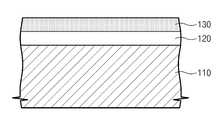
도 1a, 도 1b 및 도 1c는 본 발명의 실시예에 따른 반도체 장치의 제조 방법을 보여주는 단면도들이다.FIGS. 1A, 1B, and 1C are cross-sectional views illustrating a method of manufacturing a semiconductor device according to an embodiment of the present invention.
도 1a를 참조하면, 게이트막(110)을 형성한다. 게이트막(110)은 폴리 실리콘, 금속막 등 도전성 물질을 포함할 수 있다. 게이트막(110) 상에 블로킹 절연막(120)을 형성한다. 블로킹 절연막(120) 상에 전하 저장막(130)을 형성한다. 전하 저장막(130)은 전하를 트랩할 수 있는 실리콘 질화막 또는 폴리 실리콘을 포함할 수 있다.Referring to FIG. 1A, a
도 1b를 참조하면, 전하 저장막(130)에 열처리 공정을 수행하여 터널 절연막(140)을 형성할 수 있다. 터널 절연막(140)은 실리콘 산화막 또는 실리콘 질화 산화막을 포함할 수 있다. 상기 열처리 공정은 산화 공정 또는 질화 공정일 수 있다.Referring to FIG. 1B, the
다른 방법으로 전하 저장막(130) 상에 반도체막을 증착한 후 열처리 공정을 수행하여 반도체막을 터널 절연막(140)으로 전환할 수 있다. 반도체막은 비정질 실리콘 또는 결정질 실리콘 중 선택된 어느 하나를 포함할 수 있다. 터널 절연막(140)은 실리콘 산화막을 포함할 수 있다. 상기 열처리 공정은 산화 공정일 수 있다.Alternatively, a semiconductor film may be deposited on the
본 발명의 실시예는 2차원 메모리 반도체 장치의 게이트 스택 구조에서 실리콘 기판에 산화 공정 또는 질화 공정을 수행하여 터널 절연막을 형성하는 방법과 달리, 리버스 게이트 스택 구조(reverse gate stack structure)에서 적용되는 터널 절연막(140)의 형성 방법을 제공한다. 상기 리버스 게이트 스택 구조는 차례로 적층된 게이트막(110), 블로킹 절연막(120), 전하 저장막(130) 및 터널 절연막(140)으로 이루어질 수 있다.Unlike the method of forming a tunnel insulating film by performing an oxidation process or a nitrification process on a silicon substrate in a gate stack structure of a two-dimensional memory semiconductor device, the embodiment of the present invention can be applied to a tunnel gate structure of a reverse gate stack structure A method of forming the insulating
도 1c를 참조하면, 터널 절연막(140) 상에 활성막(160)을 형성한다. 활성막(160)은 결정질 실리콘을 포함한다.Referring to FIG. 1C, an
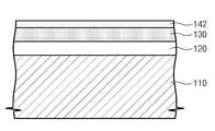
도 2a, 도 2b 및 도 2c는 본 발명의 변형 실시예에 따른 반도체 장치의 제조 방법을 보여주는 단면도들이다. 상기 변형 실시예는 앞서 설명한 실시예와 유사하다. 따라서, 설명의 간결함을 위해, 아래에서는 앞서 설명한 실시예와 중복되는 기술적 특징에 대한 설명은 개략적으로 언급되거나 생략된다.FIGS. 2A, 2B, and 2C are cross-sectional views illustrating a method of manufacturing a semiconductor device according to a modified embodiment of the present invention. The modified embodiment is similar to the previously described embodiment. Therefore, for brevity's sake, the description of the technical features overlapping with the above-described embodiment is schematically referred to or omitted.
도 2a를 참조하면, 도 1a 및 도 1b의 방법으로 차례로 적층된 게이트막(110), 블로킹 절연막(120), 전하 저장막(130) 및 제 1 터널 절연막(142)을 형성할 수 있다.Referring to FIG. 2A, a
도 2b를 참조하면, 제 1 터널 절연막(142) 상에 제 2 터널 절연막(144)을 형성할 수 있다. 제 2 터널 절연막(144)은 제 1 터널 절연막(142)에 산화 공정 또는 질화 공정을 수행하여 형성할 수 있다. 제 2 터널 절연막(144)은 실리콘 산화막 또는 실리콘 질화 산화막을 포함할 수 있다.Referring to FIG. 2B, a second
다른 방법으로, 제 1 터널 절연막(142) 상에 제 1 반도체막을 증착한 후, 상기 제 1 반도체막에 산화 공정을 수행하여 제 2 터널 절연막(144)으로 전환할 수 있다. 제 1 반도체막은 비정질 실리콘 또는 결정질 실리콘 중 선택된 어느 하나로 형성될 수 있다.Alternatively, after the first semiconductor film is deposited on the first tunnel
또 다른 방법으로, 제 2 터널 절연막(144)은 제 1 터널 절연막(142) 상에 실리콘 산화막, 실리콘 질화막 및 고유전막 중에 선택된 어느 하나를 증착하여 형성될 수 있다.Alternatively, the second
도 2c를 참조하면, 제 2 터널 절연막(144) 상에 제 3 터널 절연막(146)을 형성할 수 있다. 제 3 터널 절연막(146)은 제 2 터널 절연막(144)에 산화 공정 또는 질화 공정을 수행하여 형성될 수 있다. 제 3 터널 절연막(146)은 실리콘 산화막 또는 실리콘 질화산화막을 포함할 수 있다.Referring to FIG. 2C, a third
다른 방법으로, 제 3 터널 절연막(146) 상에 제 2 반도체막을 증착한 후 상기 제 2 반도체막에 산화 공정을 수행하여 제 3 터널 절연막(146)으로 전환할 수 있다. 제 2 반도체막은 비정질 실리콘 또는 결정질 실리콘 중 선택된 어느 하나로 형성될 수 있다.Alternatively, after the second semiconductor film is deposited on the third
또 다른 방법으로, 제 3 터널 절연막(146)은 제 2 터널 절연막(144) 상에 실리콘 산화막 및 실리콘 질화막 중 선택된 어느 하나를 증착하여 형성될 수 있다.Alternatively, the third
제 1 내지 제 3 터널 절연막들(142, 144, 146)은 일체로 전하가 터널링할 수 있는 막(148)으로 사용될 수 있다. 제 1 내지 제 3 터널 절연막들(142, 144, 146) 중 선택된 어느 하나의 막 또는 두개의 막들의 조합이 전하가 터널링할 수 있는 막으로 사용될 수 있다. 본 발명의 변형 실시예에 따르면, 제 1 내지 제 3 터널 절연막들(142, 144, 146)은 서로 다른 산소 농도 또는/및 질소 농도의 구배(gradient)를 가질 수 있다. 게다가, 제 2 터널 절연막(144)은 제 1 터널 절연막(142)과 제 3 터널 절연막(146)에 비해 유전율이 높은 막으로 형성될 수 있다.The first to third
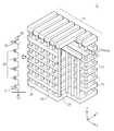
도 3은 본 발명의 실시예에 따른 반도체 장치를 도시한 사시도이다.3 is a perspective view illustrating a semiconductor device according to an embodiment of the present invention.
도 3을 참조하면, 본 발명 실시예의 반도체 장치(1)는 메모리 셀들이 포함되는 셀 영역(2)과, 메모리 셀들을 동작시키는 주변 회로가 포함되는 주변 영역(3)을 포함할 수 있다. 후술한 본 발명 실시예의 반도체 장치(1)의 구성은 본 발명의 일례이며 본 발명을 이에 한정하는 것이 아니며 다양한 변경예가 가능하다. 변경예의 일태양으로서 미국공개특허 2007/0252201에 개시된 것일 수 있으며, 이 문헌은 본 명세서에 참조문헌으로 결합될 수 있다.Referring to FIG. 3, the
셀 영역(2)은 반도체 기판(20) 상에서 Z 방향으로 수직 적층되고 X-Y 평면을 이루는 플레이트 형상의 복수개의 제어 게이트(27), 복수개의 제어 게이트(27)의 상하부에 각각 적층된 상부 선택 게이트(25)와 하부 선택 게이트(23), 상부 선택 게이트(25) 상에 적층되고 Y 방향으로 연장된 복수개의 비트라인(21), 그리고 반도체 기판(20) 상에서 Z 방향으로 수직 연장된 복수개의 활성 기둥(29: active pillar 또는 active bar)를 포함할 수 있다. 활성 기둥(29) 각각은 반도체 기판(20)에서부터 비트라인(21)까지 연장되어 상하부 선택 게이트(23,25)와 제어 게이트(27)를 관통하도록 제공될 수 있다. 반도체 기판(20)은 P 형 실리콘 기판일 수 있는데, 활성 기둥(29)은 상기 P 형 실리콘 기판에 형성된 N+ 영역 상에 형성될 수 있다. 다른 예로서, 반도체 기판(29)과 활성 기둥(29) 사이에 N+ 영역이 형성되지 않을 수 있다.The
하부 선택 게이트(23)와 상부 선택 게이트(25) 중 어느 하나는 X-Y 평면을 이루는 플레이트 형태로 제공될 수 있고 다른 하나는 X 방향으로 연장된 분리형의 라인 형태로 제공될 수 있다. 다른 예로, 하부 선택 게이트(23)와 상부 선택 게이트(25) 각각은 X 방향으로 연장된 분리형의 라인 형태로 제공될 수 있다. 본 실시예에서는 하부 선택 게이트(23)는 X-Y 평면을 이루는 플레이트형 구조이고, 상부 선택 게이트(25)는 X 방향으로 연장된 분리형의 라인 형태인 경우를 예로 들어 설명한다.Either the lower
주변 영역(3)은 복수개의 상부 선택 게이트(25)에 연결된 상부 선택 라인 구동 회로(32)와, 복수개의 제어 게이트(27)에 연결된 워드라인 구동 회로(34)와, 반도체 기판(20)의 소오스(20a)에 연결된 공통 소오스 라인(36)을 포함할 수 있다. 소오스(20a)는 반도체 기판(20)과 다른 도전형, 가령 반도체 기판(20)이 P 도전형인 경우 소오스(20a)는 N 도전형일 수 있다.The
도 4는 도 3의 셀 영역을 도시한 사시도이고, 도 5는 도 4의 메모리 트랜지스터를 도시한 사시도이다.FIG. 4 is a perspective view illustrating a cell region of FIG. 3, and FIG. 5 is a perspective view illustrating the memory transistor of FIG.
도 4 및 5를 참조하면, 활성 기둥(29)과 제어 게이트(27)는 메모리 트랜지스터(28)를 정의하고, 활성 기둥(29)과 하부 선택 게이트(23)는 하부 선택 트랜지스터(24)를 정의하고, 활성 기둥(29)과 상부 선택 게이트(25)는 상부 선택 트랜지스터(26)를 정의할 수 있다. 본 발명 실시예의 반도체 장치는 하나의 활성 기둥(29)에 형성된 복수개의 메모리 트랜지스터(28)와 상하부 트랜지스터(26,24)가 직렬로 연결되어 하나의 셀 스트링(22)을 구성하는 이른바 낸드 플래시(NAND Flash) 메모리 소자일 수 있다. 본 실시예에서 하나의 셀 스트링(22)은 4개의 메모리 트랜지스터(28)를 가지는데, 하나의 셀 스트링(22)의 메모리 트랜지스터(28)의 수는 이에 한정되지 아니하며, 메모리 용량에 의존하여 임의의 갯수로 변경될 수 있다. 활성 기둥(29)은 그 단면이 원형인 원기둥 형상일 수 있고, 또는 그 단면이 사각형인 사각기둥 형상 등 그 기둥 형상은 임의적일 수 있다.4 and 5,
메모리 트랜지스터(28) 및 상하부 선택 트랜지스터(26,24)는 활성 기둥(29)에 소오스/드레인이 존재하지 않는 이른바 공핍형(depletion) 트랜지스터로 제공될 수 있다. 다른 예로, 메모리 트랜지스터(28) 및 상하부 선택 트랜지스터(26,24)는 활성 기둥(29)에 소오스/드레인이 존재하는 이른바 증가형(enhancement) 트랜지스터로 제공될 수 있다.The
복수개의 활성 기둥(29)은 복수개의 제어 게이트(27)를 관통하는 Z 방향의 축을 갖고, 이에 따라 복수개의 제어 게이트(27)와 복수개의 활성 기둥(29) 사이의 교점들은 3차원적으로 분포될 수 있다. 본 발명 실시예의 반도체 장치의 메모리 트랜지스터(28)는 이러한 3차원적으로 분포된 교점들에 각각 형성될 수 있다. 복수개의 활성 기둥(29)과 복수개의 제어 게이트(27) 사이에는 게이트 절연막(30)이 배치될 수 있다. 게이트 절연막(30)은 본 발명의 실시예에 따른 블로킹 절연막(22), 전하 저장막(32) 및 터널 절연막(42)을 포함할 수 있다.The plurality of
도 6은 본 발명의 실시예에 따른 반도체 장치의 일부를 도시한 등가회로도이다.6 is an equivalent circuit diagram showing a part of a semiconductor device according to an embodiment of the present invention.
도 1 내지 6을 참조하면, 본 발명 실시예의 반도체 장치(1)에 있어서 복수개의 제어 게이트(27)는 복수개의 워드라인(WL1 내지 WL4)으로 사용되고, 복수개의 상부 선택 게이트(25)는 복수개의 상부 선택 라인(USL1 내지 USL3)으로 사용되고, 하부 선택 게이트(23)는 하부 선택 라인(LSL)으로 사용된다. 셀 스트링(22)은 복수개의 비트라인(BL1 내지 BL3) 각각에 복수개 연결될 수 있다.1 to 6, in the
복수개의 제어 게이트(27) 각각은 2차원적으로 펼쳐져 있는 평판형 구조를 이룰 수 있으므로 복수개의 워드라인(WL1 내지 WL4) 각각은 평면 구조를 가지며 셀 스트링(22)에 대해 실질적으로 수직일 수 있다. 복수개의 워드라인(WL1 내지 WL4)에는 복수개의 메모리 트랜지스터(28)가 3차원적으로 분포될 수 있다.Each of the plurality of
상부 선택 게이트(25)는 X 방향으로 연장된 분리형 배선 구조를 이룰 수 있으므로 복수개의 상부 선택 라인(USL1 내지 USL3)은 복수개의 비트라인(BL1 내지 BL3)을 가로지도록 배치될 수 있다. 복수개의 상부 선택 라인(USL1 내지 USL3) 각각은 복수개의 비트라인(BL1 내지 BL3) 각각과 전기적으로 연결되므로 하나의 셀 스트링(22)이 독립적으로 선택될 수 있다.The upper
하부 선택 게이트(23)는 2차원적으로 펼쳐져 있는 평판평 구조를 이룰 수 있으므로 하부 선택 라인(LSL)은 평면 구조를 가지며 셀 스트링(22)에 대해 실질적으로 수직일 수 있다. 하부 선택 라인(LSL)은 활성 기둥(29)과 반도체 기판(20) 사이의 전기적 연결을 제어할 수 있다.The lower select gate LSL may have a planar structure and may be substantially perpendicular to the
본 발명 실시예의 반도체 장치(1)에 있어서 프로그램 동작은 선택된 워드라인(WL)과 활성 기둥(29) 사이에 전압차를 설정하여 전하를 전하저장막에 주입함으로써 구현될 수 있다. 일례로, 선택된 워드라인(WL)에 프로그램 전압(Vprog)을 인가하므로써 파울러-노던하임 터널링 현상을 이용하여 활성 기둥(29)으로부터 프로그램하고자 하는 워드라인(WL)에 속한 메모리 트랜지스터(28)의 전하저장막으로 전 자를 주입하여 프로그램을 구현할 수 있다. 선택된 워드라인(WL)에 인가된 프로그램 전압은 비선택 워드라인에 속한 메모리 트랜지스터를 프로그램시킬 수 있으므로, 부스팅 기술을 이용하여 의도되지 않는 프로그램을 방지할 수 있다.In the
판독 동작은 판독하고자 하는 메모리 트랜지스터(28)가 연결된 워드라인(WL)에 가령 OV 로 설정하고 다른 워드라인에는 읽기 전압(Vread)을 설정한다. 그 결과, 판독하고자 하는 메모리 트랜지스터(28)의 문턴 전압(Vth)이 기존 전압보다 큰지 또는 작은지에 의존하여 비트라인(BL)에 전류가 충전되는지가 결정되며, 이에 따라 비트라인(BL)의 전류를 감지하므로써 판독하고자 하는 메모리 트랜지스터(28)의 데이터 정보가 판독될 수 있다.The read operation sets the read voltage Vread to the word line WL to which the
소거 동작은 이른바 "게이트 유도 드레인 누설전류(GIDL)"를 이용하여 블록 단위로 수행될 수 있다. 일례로, 선택된 비트라인(BL)과 기판(20)에 소거 전압(Verase)을 인가하므로써 활성 기둥(29)의 전위를 상승시킨다. 이때, 활성 기둥(29)의 전위는 약간 지연되면서 상승되도록 할 수 있다. 이에 수반하여, 하부 선택 게이트(24)의 단자에서 GIDL이 발생하고, GIDL에 의해 생성된 전자는 기판(20)으로 방출되고 생성된 정공은 활성 기둥(29)으로 방출된다. 이로 인해 소거 전압(Verase) 근처의 전위가 메모리 트랜지스터(28)의 채널, 즉 활성 기둥(29)으로 전달될 수 있다. 이때, 워드라인(WL)의 전위를 OV 로 설정되면 메모리 트랜지스터(28)에 축적된 전자들이 빠져나오게 되어 데이터 소거가 구현될 수 있다. 한편, 의도되지 않은 소거 동작이 행해지지 않도록 비선택 블록의 워드라인을 플로팅시킬 수 있다.The erase operation can be performed block by block using the so-called " gate induced drain leakage current (GIDL) ". For example, the potential of the
본 발명의 실시예에 따른 반도체 장치(1)의 동작 방법은 본 발명의 기술적 사상을 예시적으로 설명하기 위한 것이며, 본 발명의 기술적 특징이 이에 한정되는 것은 아니다. 따라서, 이 분야에 종사하는 통상의 지식을 가진 자라면, 공지된 기술들에 기초하여 이러한 변형을 구현하는 것은 용이하다는 것은 자명하므로, 동작 방법과 관련된 본 발명의 기술적 특징은 공지된 기술들에 기초하여 다양하게 변형되어 구현될 수 있다. 일례로, 본 명세서에 참조문헌으로 결합된 미국공개특허 2007/0252201에 개시된 방법으로 반도체 장치(1)의 동작이 구현될 수 있다.The operation method of the
도 7a, 도 7b, 도 7c 및 도 7d는 본 발명의 실시예에 따른 반도체 장치의 제조 방법을 보여주는 단면도들이다.FIGS. 7A, 7B, 7C, and 7D are cross-sectional views illustrating a method of manufacturing a semiconductor device according to an embodiment of the present invention.
도 7a를 참조하면, 반도체 기판(200)이 준비된다. 반도체 기판(200)은 제 1 도전형을 갖는 단결정 구조의 반도체, 가령 p형 실리콘 웨이퍼로 형성될 수 있다. 반도체 기판(200)은 다른 도전형의 불순물 영역들에 의해 전기적으로 분리된 영역, 즉 웰 영역을 구비할 수 있다. 웰 영역은 포켓 웰 또는 삼중 웰 구조로 형성될 수 있다. 반도체 기판(200) 상에 식각 저지막(205)을 형성할 수 있다. 식각 저지막(205)은 실리콘 산화막일 수 있다. 식각 저지막(205)은 커패시터 유전막으로 사용될 수 있다.Referring to FIG. 7A, a
식각 저지막(205) 상에 도전막 그룹(210) 및 절연막 그룹(250)을 형성할 수 있다. 도전막 그룹(210)은 복수개의 도전막들(211, 212, 213, 214, 215, 216)을 포함한다. 절연막 그룹(250)은 복수개의 절연막들(251, 252, 253, 254, 255, 256)을 포함한다. 도전막들(211~216)과 절연막들(251~256)은 교대로 형성된다. 도전막 들(211~216)은 도핑된 다결정 실리콘 또는 금속을 증착하여 형성될 수 있다. 최하부 도전막(211)은 하부 선택 게이트로 사용될 수 있다. 최상부 도전막(216)은 상부 선택 게이트로 사용될 수 있다. 상부 및 하부 선택 게이트들로 사용되는 도전막들(216, 211) 사이의 도전막들(212, 213, 214, 215)은 제어 게이트로 사용될 수 있다. 상기 도전막들(212~215)은 서로 같은 두께로 증착될 수 있다. 상기 도전막들(212~215)의 두께는 채널 길이를 결정할 수 있으므로 상기 도전막들(212~215)의 두께는 단채널에 따른 전기적 특성의 문제점을 해결할 수 있는 범위에서 선택될 수 있다.The
절연막들(251~256)은 실리콘 산화막을 증착하여 형성할 수 있다. 다른 예로, 절연막들(251~256)은 고유전막으로 형성할 수 있다. 일례로, 절연막들(251~256)은 실리콘 산화막에 비해 높은 유전 상수를 갖는 물질(예: 실리콘 질화막, 실리콘 산화질화막)을 증착하여 형성할 수 있다.The insulating
절연막 그룹(250)과 도전막 그룹(210)을 구성하는 박막들의 수, 그들의 두께, 그 들의 물질은 메모리 트랜지스터의 전기적 특성 및 이들을 패터닝하는 공정에서의 기술적 어려움을 고려하여 다양하게 변경될 수 있다. 절연막 그룹(250)과 도전막 그룹(210)은 계단 형상을 이루도록 형성할 수 있다.The number of the thin films constituting the insulating
도 7b를 참조하면, 도전막 그룹(210) 및 절연막 그룹(250)를 패터닝하여, 상기 반도체기판(100)을 노출시키는 개구부(290)를 형성한다. 이미 언급한 바와 같이, 트랜지스터의 균일한 전기적 특성을 구현하기 위해 개구부(290)는 수직한 측벽을 갖도록 가령 드라이 에칭 기술을 사용하여 형성할 수 있다. 상기 패터닝 공정은 식각 저지막(205)이 제거될 때까지 수행될 수 있다. 개구부(290)는 반도체기판(100)의 상부면(202)을 노출할 수 있다. 개구부(290)의 측벽은 도전막 그룹(210)의 도전막들(211, 212, 213, 214, 215, 216)의 노출된 측면을 포함한다.Referring to FIG. 7B, the
개구부(290)의 측벽에 도전막들(211, 212, 213, 214, 215, 216)의 노출된 측면을 덮는 게이트 절연막(280)을 형성한다. 게이트 절연막(280)은 블로킹 절연막(220), 전하 저장막(230) 및 터널 절연막(240)으로 구성된다. 도 1a 및 도 1b를 참조하여 설명한 것과 동일 또는 유사하는 공정을 실시하여, 측면 방향으로 적층되는 블로킹 절연막(220), 전하 저장막(230) 및 터널 절연막(240)을 형성할 수 있다. 즉, 3 차원 반도체 메모리 장치의 게이트 구조에 본 발명의 실시예들에 따른 터널 절연막의 형성 방법이 적용될 수 있다.A
도 7c를 참조하면, 상기 개구부(290)의 측벽에 스페이서(262)가 형성될 수 있다. 스페이서(262)를 식각 마스크로 사용하여 게이트 절연막(280)의 일부를 식각하여 반도체 기판(200)을 노출할 수 있다. 스페이서(262)는 개구부(290) 내에서 게이트 절연막(280)의 내측벽을 덮도록 형성되어, 반도체 기판(200)의 상부면(202)을 노출하기 위한 식각 공정에서 게이트 절연막(280)에 대한 식각 손상을 감소시킨다.Referring to FIG. 7C, a
개구부(290)를 채우는 활성 기둥(260)을 형성한다. 활성 기둥(260)은 반도체 기판(200)과 동일한 물질로 형성될 수 있다. 활성 기둥(260)은 에피택시얼 공정을 수행하여 상기 노출된 반도체 기판(200)으로부터 성장하여 형성될 수 있다. 이 경우 반도체 기판(200)과 활성 기둥(260)은 결정 결함없이 연속적으로 이어지는 단결정 구조의 실리콘일 수 있다. 스페이서(262)가 실리콘으로 형성되는 경우, 스페이 서(262)는 상기 에피택시얼 공정 동안 단결정화되어 상기 활성 기둥(260)의 일부를 구성할 수 있다. 활성 기둥(260)은 반도체 기판(200)과 동일한 도전형을 갖도록 형성될 수 있다. 일례로, 반도체 기판(200)과 활성 기둥(260)은 P형일 수 있다. 이러한 결과, 활성 기둥(260)과 반도체 기판(200) 사이에는 다이오드를 구성하지 않기 때문에 활성 기둥(260)과 반도체 기판(200)과 등전위를 가질 수 있다.Thereby forming the
도 7d를 참조하면, 활성 기둥(260) 상에 활성 기둥(260)과 전기적으로 연결되는 비트라인(270)을 형성할 수 있다. 비트라인(610)은 상부 선택 게이트를 가로지는 방향으로 연장된 형태로 형성할 수 있다.Referring to FIG. 7D, a
도 8는 본 발명의 실시예들에 따른 반도체 장치를 포함하는 전자 시스템을 나타내는 블럭도이다.8 is a block diagram illustrating an electronic system including a semiconductor device according to embodiments of the present invention.
도 8을 참조하면, 전자 시스템(400)은 제어기(410), 입출력 장치(420) 및 기억 장치(430)를 포함할 수 있다. 상기 제어기(410), 입출력 장치(420) 및 기억 장치(430)는 버스(450, bus)를 통하여 서로 커플링(coupling)될 수 있다. 상기 버스(450)는 데이터들 및/또는 동작 신호들이 이동하는 통로에 해당한다. 상기 제어기(410)는 적어도 하나의 마이크로프로세서, 디지털 신호 프로세서, 마이크로컨트롤러, 및 이들과 유사한 기능을 수행할 수 있는 논리 소자들 중에서 적어도 하나를 포함할 수 있다. 상기 입출력 장치(420)는 키패드, 키보드 및 표시 장치(display device)등에서 선택된 적어도 하나를 포함할 수 있다. 상기 기억 장치(430)는 데이터를 저장하는 장치이다. 상기 기억 장치(430)는 데이터 및/또는 상기 제어기(410)에 의해 실행되는 명령어 등을 저장할 수 있다. 상기 기억 장치(430)는 상술한 실 시예 또는 변형 실시예에 따른 반도체 메모리 장치를 포함할 수 있다. 상기 전자 시스템(400)은 통신 네트워크로 데이터를 전송하거나 통신 네트워크로부터 데이터를 수신하기 위한 인터페이스(440)를 더 포함할 수 있다. 상기 인터페이스(440)는 유선 또는 무선 형태일 수 있다. 예컨대, 상기 인터페이스(440)는 안테나 또는 유무선 트랜시버등을 포함할 수 있다.8, the
상기 전자 시스템(400)은 모바일 시스템, 개인용 컴퓨터, 산업용 컴퓨터 또는 다양한 기능을 수행하는 시스템 등으로 구현될 수 있다. 예컨대, 상기 모바일 시스템은 개인 휴대용 정보 단말기(PDA; Personal Digital Assistant), 휴대용 컴퓨터, 웹 타블렛(web tablet), 모바일폰(mobile phone), 무선폰(wireless phone), 랩톱(laptop) 컴퓨터, 메모리 카드, 디지털 뮤직 시스템(digital music system) 또는 정보 전송/수신 시스템 등일 수 있다. 상기 전자 시스템(400)이 무선 통신을 수행할 수 있는 장비인 경우에, 상기 전자 시스템(400)은 CDMA, GSM, NADC, E-TDMA, WCDAM, CDMA2000 같은 3세대 통신 시스템 같은 통신 인터페이스 프로토콜에서 사용될 수 있다.The
도 9는 본 발명의 실시예들에 따른 반도체 장치를 포함하는 메모리 카드를 나타내는 블럭도이다.9 is a block diagram showing a memory card including a semiconductor device according to embodiments of the present invention.
도 9를 참조하면, 메모리 카드(500)는 기억 장치(510) 및 메모리 제어기(520)를 포함한다. 상기 기억 장치(510)는 데이터를 저장할 수 있다. 상기 기억 장치(510)는 전원 공급이 중단될지라도 저장된 데이터를 그대로 유지하는 비휘발성 특성을 갖는 것이 바람직하다. 상기 기억 장치(510)는 상술한 실시예 또는 변형 실 시예에 따른 반도체 메모리 장치를 포함할 수 있다. 상기 메모리 제어기(520)는 호스트(host)의 판독/쓰기 요청에 응답하여 상기 기억 장치(510)에 저장된 데이터를 독출하거나, 상기 기억 장치(510)에 데이터를 저장할 수 있다.Referring to FIG. 9, the
본 발명의 실시예들에 따른 플래시 메모리 또는 플래시 메모리 시스템은 다양한 형태의 패키지로 실장될 수 있다. 예를 들면, 본 발명의 실시예들에 따른 플래시 메모리 또는 플래시 메모리 시스템은 패키지 온 패키지(Package on Package), 볼 그리드 어레이(Ball Grid Arrays), 칩 스케일 패키지(Chip scale packages), 플라스틱 리드 칩 캐리어(Plastic Leaded Chip Carrier), 플라스틱 듀얼 인라인 패키지(Plastic Dual In-Line Package), 멀티 칩 패키지(Multi Chip Package), 웨이퍼 레벨 패키지(Wafer Level Package), 웨이퍼 레벨 제조 패키지(Wafer Level Fabricated Package), 웨이퍼 레벨 프로세스 스택 패키지(Wafer Level Processed Stack Package), 다이 온 와플 패키지(Die On Waffle Package), 다이 인 웨이퍼 폼(Die in Wafer Form), 칩 온 보오드(Chip On Board), 세라믹 듀얼 인라인 패키지(Ceramic Dual In-Line Package), 플라스킥 메트릭 쿼드 플랫 패키지(Plastic Metric Quad Flat Pack), 씬 쿼드 플랫 패키지(Thin Quad Flat Pack), 스몰 아웃라인 패키지(Small Outline Package), 축소 스몰 아웃라인 패키지(Shrink Small Outline Package), 씬 스몰 아웃라인 패키지(Thin Small Outline Package), 씬 쿼드 플랫 패키지(Thin Quad Flat Package), 시스템 인 패키지(System In Package) 등과 같은 방식으로 패키징될 수 있다.The flash memory or flash memory system according to embodiments of the present invention may be implemented in various types of packages. For example, the flash memory or flash memory system according to embodiments of the present invention may be implemented as a package on package, ball grid arrays, chip scale packages, (Plastic Leaded Chip Carrier), Plastic Dual In-Line Package, Multi Chip Package, Wafer Level Package, Wafer Level Fabricated Package, Level process stack package, Die On Waffle Package, Die in Wafer Form, Chip On Board, Ceramic Dual in-line package In-Line Package, Plastic Metric Quad Flat Pack, Thin Quad Flat Pack, Small Outline Pack age, etc., Shrink Small Outline Package, Thin Small Outline Package, Thin Quad Flat Package, and System In Package. Can be packaged.
도 1a, 도 1b 및 도 1c는 본 발명의 실시예에 따른 반도체 장치의 제조 방법을 보여주는 단면도들이다.FIGS. 1A, 1B, and 1C are cross-sectional views illustrating a method of manufacturing a semiconductor device according to an embodiment of the present invention.
도 2a, 도 2b 및 도 2c는 본 발명의 변형 실시예에 따른 반도체 장치의 제조 방법을 보여주는 단면도들이다.FIGS. 2A, 2B, and 2C are cross-sectional views illustrating a method of manufacturing a semiconductor device according to a modified embodiment of the present invention.
도 3은 본 발명의 실시예에 따른 반도체 장치를 도시한 사시도이다.3 is a perspective view illustrating a semiconductor device according to an embodiment of the present invention.
도 4는 도 3의 셀 영역을 도시한 사시도이고, 도 5는 도 4의 메모리 트랜지스터를 도시한 사시도이다.FIG. 4 is a perspective view illustrating a cell region of FIG. 3, and FIG. 5 is a perspective view illustrating the memory transistor of FIG.
도 6은 본 발명의 실시예에 따른 반도체 장치의 일부를 도시한 등가회로도이다.6 is an equivalent circuit diagram showing a part of a semiconductor device according to an embodiment of the present invention.
도 7a, 도 7b, 도 7c 및 도 7d는 본 발명의 실시예에 따른 반도체 장치의 제조 방법을 보여주는 단면도들이다.FIGS. 7A, 7B, 7C, and 7D are cross-sectional views illustrating a method of manufacturing a semiconductor device according to an embodiment of the present invention.
도 8는 본 발명의 실시예들에 따른 반도체 장치를 포함하는 전자 시스템을 나타내는 블럭도이다.8 is a block diagram illustrating an electronic system including a semiconductor device according to embodiments of the present invention.
도 9는 본 발명의 실시예들에 따른 반도체 장치를 포함하는 메모리 카드를 나타내는 블럭도이다.9 is a block diagram showing a memory card including a semiconductor device according to embodiments of the present invention.
Claims (26)
Translated fromKoreanPriority Applications (4)
| Application Number | Priority Date | Filing Date | Title |
|---|---|---|---|
| KR1020090001979AKR101512494B1 (en) | 2009-01-09 | 2009-01-09 | Method for manufacturing semiconductor device |
| US12/654,881US8460998B2 (en) | 2009-01-09 | 2010-01-07 | Method of fabricating semiconductor device |
| US13/912,441US9293335B2 (en) | 2009-01-09 | 2013-06-07 | Method of fabricating semiconductor device |
| US15/070,247US9716102B2 (en) | 2009-01-09 | 2016-03-15 | Semiconductor device |
Applications Claiming Priority (1)
| Application Number | Priority Date | Filing Date | Title |
|---|---|---|---|
| KR1020090001979AKR101512494B1 (en) | 2009-01-09 | 2009-01-09 | Method for manufacturing semiconductor device |
Publications (2)
| Publication Number | Publication Date |
|---|---|
| KR20100082608A KR20100082608A (en) | 2010-07-19 |
| KR101512494B1true KR101512494B1 (en) | 2015-04-16 |
Family
ID=42319366
Family Applications (1)
| Application Number | Title | Priority Date | Filing Date |
|---|---|---|---|
| KR1020090001979AActiveKR101512494B1 (en) | 2009-01-09 | 2009-01-09 | Method for manufacturing semiconductor device |
Country Status (2)
| Country | Link |
|---|---|
| US (3) | US8460998B2 (en) |
| KR (1) | KR101512494B1 (en) |
Families Citing this family (25)
| Publication number | Priority date | Publication date | Assignee | Title |
|---|---|---|---|---|
| US20090179253A1 (en) | 2007-05-25 | 2009-07-16 | Cypress Semiconductor Corporation | Oxide-nitride-oxide stack having multiple oxynitride layers |
| US8940645B2 (en) | 2007-05-25 | 2015-01-27 | Cypress Semiconductor Corporation | Radical oxidation process for fabricating a nonvolatile charge trap memory device |
| US8680601B2 (en) | 2007-05-25 | 2014-03-25 | Cypress Semiconductor Corporation | Nonvolatile charge trap memory device having a deuterated layer in a multi-layer charge-trapping region |
| US9449831B2 (en) | 2007-05-25 | 2016-09-20 | Cypress Semiconductor Corporation | Oxide-nitride-oxide stack having multiple oxynitride layers |
| US8633537B2 (en) | 2007-05-25 | 2014-01-21 | Cypress Semiconductor Corporation | Memory transistor with multiple charge storing layers and a high work function gate electrode |
| US9716153B2 (en)* | 2007-05-25 | 2017-07-25 | Cypress Semiconductor Corporation | Nonvolatile charge trap memory device having a deuterated layer in a multi-layer charge-trapping region |
| KR101512494B1 (en) | 2009-01-09 | 2015-04-16 | 삼성전자주식회사 | Method for manufacturing semiconductor device |
| JP2012069709A (en)* | 2010-09-22 | 2012-04-05 | Toshiba Corp | Semiconductor memory |
| KR20120060480A (en)* | 2010-12-02 | 2012-06-12 | 삼성전자주식회사 | Vertical structure non-volatile memory device, semiconductor device and system |
| KR20130072523A (en)* | 2011-12-22 | 2013-07-02 | 에스케이하이닉스 주식회사 | Three dimension non-volatile memory device and method of manufacturing the same |
| KR102115156B1 (en)* | 2012-07-01 | 2020-05-27 | 사이프레스 세미컨덕터 코포레이션 | Nonvolatile charge trap memory device having a deuterated layer in a multy-layer charge-trapping region |
| KR102015578B1 (en)* | 2012-09-11 | 2019-08-28 | 삼성전자주식회사 | Nonvolatile memory device and manufactureing the same |
| CN104103639B (en)* | 2013-04-03 | 2018-04-13 | 群联电子股份有限公司 | NAND flash memory unit, operation method and reading method |
| US9224749B1 (en)* | 2014-06-04 | 2015-12-29 | Macronix International Co., Ltd. | Method for filling polysilicon gate in semiconductor devices, and semiconductor devices |
| KR102263315B1 (en)* | 2014-08-06 | 2021-06-15 | 삼성전자주식회사 | Semiconductor device and manufacturing method of semiconductor device |
| US9230979B1 (en)* | 2014-10-31 | 2016-01-05 | Sandisk Technologies Inc. | High dielectric constant etch stop layer for a memory structure |
| CN106298472B (en)* | 2015-05-14 | 2019-01-18 | 旺宏电子股份有限公司 | Method for forming semiconductor structure |
| US9768191B2 (en)* | 2015-10-19 | 2017-09-19 | Toshiba Memory Corporation | Semiconductor device |
| US9837431B2 (en)* | 2015-11-20 | 2017-12-05 | Sandisk Technologies Llc | 3D semicircular vertical NAND string with recessed inactive semiconductor channel sections |
| US10032790B2 (en)* | 2015-12-16 | 2018-07-24 | Toshiba Memory Corporation | Semiconductor device |
| US10128265B2 (en)* | 2017-01-18 | 2018-11-13 | Micron Technology, Inc. | Memory cells, integrated structures and memory arrays |
| US11195847B2 (en)* | 2019-05-15 | 2021-12-07 | Macronix International Co., Ltd. | Memory device and method for forming the same |
| KR102728797B1 (en) | 2019-07-31 | 2024-11-11 | 삼성전자주식회사 | Semiconductor devices and operating method for the same |
| KR102711222B1 (en) | 2019-09-04 | 2024-09-27 | 삼성전자주식회사 | Vertical non-volatile memory devices and methods of programming in the same |
| US11895841B2 (en) | 2021-09-27 | 2024-02-06 | Macronix International Co., Ltd. | Memory structure and manufacturing method for the same |
Family Cites Families (31)
| Publication number | Priority date | Publication date | Assignee | Title |
|---|---|---|---|---|
| JPH0582795A (en)* | 1991-08-22 | 1993-04-02 | Rohm Co Ltd | Semiconductor memory device |
| US5126290A (en)* | 1991-09-11 | 1992-06-30 | Micron Technology, Inc. | Method of making memory devices utilizing one-sided ozone teos spacers |
| US5397748A (en)* | 1991-12-28 | 1995-03-14 | Nec Corporation | Method of producing semiconductor device with insulating film having at least silicon nitride film |
| US5619063A (en)* | 1993-07-07 | 1997-04-08 | Actel Corporation | Edgeless, self-aligned, differential oxidation enhanced and difusion-controlled minimum-geometry antifuse and method of fabrication |
| JPH1093083A (en) | 1996-09-18 | 1998-04-10 | Toshiba Corp | Method for manufacturing semiconductor device |
| US5851878A (en)* | 1997-04-01 | 1998-12-22 | United Microelectronics Corporation | Method of forming a rugged polysilicon fin structure in DRAM |
| US6297092B1 (en)* | 1998-12-02 | 2001-10-02 | Micron Technology, Inc. | Method and structure for an oxide layer overlaying an oxidation-resistant layer |
| JP4226205B2 (en)* | 2000-08-11 | 2009-02-18 | 富士雄 舛岡 | Manufacturing method of semiconductor memory device |
| KR100483035B1 (en)* | 2001-03-30 | 2005-04-15 | 샤프 가부시키가이샤 | A semiconductor memory and its production process |
| JP4104834B2 (en)* | 2001-04-13 | 2008-06-18 | 株式会社東芝 | Manufacturing method of MIS field effect transistor |
| US6518200B2 (en)* | 2001-06-07 | 2003-02-11 | Taiwan Semiconductor Manufacturing Co., Ltd. | Graded composite layer and method for fabrication thereof |
| JP3963664B2 (en)* | 2001-06-22 | 2007-08-22 | 富士雄 舛岡 | Semiconductor memory device and manufacturing method thereof |
| US7473959B2 (en)* | 2001-06-28 | 2009-01-06 | Samsung Electronics Co., Ltd. | Non-volatile semiconductor memory devices and methods of fabricating the same |
| US20030017670A1 (en)* | 2001-07-20 | 2003-01-23 | Macronix International Co., Ltd. | Method of manufacturing a semiconductor memory device with a gate dielectric stack |
| US6803275B1 (en)* | 2002-12-03 | 2004-10-12 | Fasl, Llc | ONO fabrication process for reducing oxygen vacancy content in bottom oxide layer in flash memory devices |
| KR100657910B1 (en) | 2004-11-10 | 2006-12-14 | 삼성전자주식회사 | Multi-bit Flash Memory Device, Operation Method thereof, and Manufacturing Method Thereof |
| US7612403B2 (en)* | 2005-05-17 | 2009-11-03 | Micron Technology, Inc. | Low power non-volatile memory and gate stack |
| US7829938B2 (en)* | 2005-07-14 | 2010-11-09 | Micron Technology, Inc. | High density NAND non-volatile memory device |
| JP5016832B2 (en)* | 2006-03-27 | 2012-09-05 | 株式会社東芝 | Nonvolatile semiconductor memory device and manufacturing method thereof |
| JP2007317874A (en) | 2006-05-25 | 2007-12-06 | Toshiba Corp | Nonvolatile semiconductor memory device |
| US8143661B2 (en)* | 2006-10-10 | 2012-03-27 | Spansion Llc | Memory cell system with charge trap |
| JP4772656B2 (en) | 2006-12-21 | 2011-09-14 | 株式会社東芝 | Nonvolatile semiconductor memory |
| JP2008182035A (en) | 2007-01-24 | 2008-08-07 | Toshiba Corp | Semiconductor memory device and manufacturing method thereof |
| US20090179253A1 (en)* | 2007-05-25 | 2009-07-16 | Cypress Semiconductor Corporation | Oxide-nitride-oxide stack having multiple oxynitride layers |
| US8643124B2 (en)* | 2007-05-25 | 2014-02-04 | Cypress Semiconductor Corporation | Oxide-nitride-oxide stack having multiple oxynitride layers |
| JP2009027134A (en)* | 2007-06-21 | 2009-02-05 | Tokyo Electron Ltd | MOS type semiconductor memory device |
| JP2009267366A (en)* | 2008-04-02 | 2009-11-12 | Nec Electronics Corp | Semiconductor memory and method of manufacturing the same |
| US7732891B2 (en)* | 2008-06-03 | 2010-06-08 | Kabushiki Kaisha Toshiba | Semiconductor device |
| US7910979B2 (en)* | 2008-07-08 | 2011-03-22 | Kabushiki Kaisha Toshiba | Nonvolatile semiconductor memory device |
| US8097911B2 (en)* | 2008-12-31 | 2012-01-17 | Intel Corporation | Etch stop structures for floating gate devices |
| KR101512494B1 (en)* | 2009-01-09 | 2015-04-16 | 삼성전자주식회사 | Method for manufacturing semiconductor device |
- 2009
- 2009-01-09KRKR1020090001979Apatent/KR101512494B1/enactiveActive
- 2010
- 2010-01-07USUS12/654,881patent/US8460998B2/enactiveActive
- 2013
- 2013-06-07USUS13/912,441patent/US9293335B2/enactiveActive
- 2016
- 2016-03-15USUS15/070,247patent/US9716102B2/enactiveActive
Also Published As
| Publication number | Publication date |
|---|---|
| US9716102B2 (en) | 2017-07-25 |
| US20130273728A1 (en) | 2013-10-17 |
| US9293335B2 (en) | 2016-03-22 |
| KR20100082608A (en) | 2010-07-19 |
| US20100178759A1 (en) | 2010-07-15 |
| US20160197086A1 (en) | 2016-07-07 |
| US8460998B2 (en) | 2013-06-11 |
Similar Documents
| Publication | Publication Date | Title |
|---|---|---|
| KR101512494B1 (en) | Method for manufacturing semiconductor device | |
| KR101760658B1 (en) | Non-volatile memory device | |
| US9035372B2 (en) | Nonvolatile memory device, fabrication method thereof and memory system comprising the same | |
| US7982260B2 (en) | Semiconductor memory device | |
| KR100640620B1 (en) | NOR type flash memory device of twin bit cell structure and manufacturing method thereof | |
| KR101845507B1 (en) | Non-volatile memory device having vertical structure and method for manufacturing the same | |
| US8785276B2 (en) | Methods for fabricating a cell string and a non-volatile memory device including the cell string | |
| KR101483533B1 (en) | Non-volatile memroy device and method for the same | |
| US8987797B2 (en) | Nonvolatile memory device and method of forming the same | |
| CN111613623A (en) | Three-dimensional flash memory device with increased storage density | |
| CN108231789A (en) | Include the semiconductor memory system of protrusion pad | |
| CN102956644B (en) | There is nonvolatile semiconductor memory member and the manufacture method thereof of vertical memory cell | |
| KR20120085603A (en) | Non-volatile memory device, method of operating the same, and method of fabricating the same | |
| US10115737B2 (en) | Charge storage region in non-volatile memory | |
| KR101136140B1 (en) | Bitline implant utilizing dual poly | |
| KR20170018996A (en) | Semiconductor devices | |
| KR100784930B1 (en) | Memory Cells with Vertical Channel Double Gate Structures | |
| KR102612197B1 (en) | Semiconductor device | |
| TW202218123A (en) | Integrated assemblies, and methods of forming integrated assemblies | |
| US9171622B2 (en) | Non-volatile memory device and method of fabricating the same | |
| KR101660243B1 (en) | Non-volatile memory device and fabricating method the device | |
| US20220399276A1 (en) | Semiconductor device and manufacturing method thereof | |
| US7692236B1 (en) | Multiple dual bit memory integrated circuit system | |
| KR20120015930A (en) | Nonvolatile Memory Device and Formation Method | |
| KR20120085468A (en) | Non-volatile memory device, method of operating the same, and method of fabricating the same |
Legal Events
| Date | Code | Title | Description |
|---|---|---|---|
| PA0109 | Patent application | Patent event code:PA01091R01D Comment text:Patent Application Patent event date:20090109 | |
| PG1501 | Laying open of application | ||
| A201 | Request for examination | ||
| PA0201 | Request for examination | Patent event code:PA02012R01D Patent event date:20140103 Comment text:Request for Examination of Application Patent event code:PA02011R01I Patent event date:20090109 Comment text:Patent Application | |
| E902 | Notification of reason for refusal | ||
| PE0902 | Notice of grounds for rejection | Comment text:Notification of reason for refusal Patent event date:20141224 Patent event code:PE09021S01D | |
| E701 | Decision to grant or registration of patent right | ||
| PE0701 | Decision of registration | Patent event code:PE07011S01D Comment text:Decision to Grant Registration Patent event date:20150330 | |
| PR0701 | Registration of establishment | Comment text:Registration of Establishment Patent event date:20150409 Patent event code:PR07011E01D | |
| PR1002 | Payment of registration fee | Payment date:20150410 End annual number:3 Start annual number:1 | |
| PG1601 | Publication of registration | ||
| PR1001 | Payment of annual fee | Payment date:20180330 Start annual number:4 End annual number:4 | |
| FPAY | Annual fee payment | Payment date:20190329 Year of fee payment:5 | |
| PR1001 | Payment of annual fee | Payment date:20190329 Start annual number:5 End annual number:5 | |
| PR1001 | Payment of annual fee | Payment date:20200330 Start annual number:6 End annual number:6 | |
| PR1001 | Payment of annual fee | Payment date:20210329 Start annual number:7 End annual number:7 | |
| PR1001 | Payment of annual fee | Payment date:20220323 Start annual number:8 End annual number:8 | |
| PR1001 | Payment of annual fee | Payment date:20230327 Start annual number:9 End annual number:9 | |
| PR1001 | Payment of annual fee | Payment date:20240325 Start annual number:10 End annual number:10 | |
| PR1001 | Payment of annual fee | Payment date:20250325 Start annual number:11 End annual number:11 |