KR101508418B1 - Predictive control of power converter for led driver - Google Patents
Predictive control of power converter for led driverDownload PDFInfo
- Publication number
- KR101508418B1 KR101508418B1KR20120143254AKR20120143254AKR101508418B1KR 101508418 B1KR101508418 B1KR 101508418B1KR 20120143254 AKR20120143254 AKR 20120143254AKR 20120143254 AKR20120143254 AKR 20120143254AKR 101508418 B1KR101508418 B1KR 101508418B1
- Authority
- KR
- South Korea
- Prior art keywords
- led
- switching
- power converter
- controller
- switching power
- Prior art date
- Legal status (The legal status is an assumption and is not a legal conclusion. Google has not performed a legal analysis and makes no representation as to the accuracy of the status listed.)
- Active
Links
Images


Classifications
- H—ELECTRICITY
- H05—ELECTRIC TECHNIQUES NOT OTHERWISE PROVIDED FOR
- H05B—ELECTRIC HEATING; ELECTRIC LIGHT SOURCES NOT OTHERWISE PROVIDED FOR; CIRCUIT ARRANGEMENTS FOR ELECTRIC LIGHT SOURCES, IN GENERAL
- H05B45/00—Circuit arrangements for operating light-emitting diodes [LED]
- H05B45/30—Driver circuits
- H05B45/37—Converter circuits
- H05B45/3725—Switched mode power supply [SMPS]
- H05B45/375—Switched mode power supply [SMPS] using buck topology
- H—ELECTRICITY
- H05—ELECTRIC TECHNIQUES NOT OTHERWISE PROVIDED FOR
- H05B—ELECTRIC HEATING; ELECTRIC LIGHT SOURCES NOT OTHERWISE PROVIDED FOR; CIRCUIT ARRANGEMENTS FOR ELECTRIC LIGHT SOURCES, IN GENERAL
- H05B45/00—Circuit arrangements for operating light-emitting diodes [LED]
- H05B45/30—Driver circuits
- H05B45/37—Converter circuits
- H05B45/3725—Switched mode power supply [SMPS]
- H05B45/38—Switched mode power supply [SMPS] using boost topology
- H—ELECTRICITY
- H05—ELECTRIC TECHNIQUES NOT OTHERWISE PROVIDED FOR
- H05B—ELECTRIC HEATING; ELECTRIC LIGHT SOURCES NOT OTHERWISE PROVIDED FOR; CIRCUIT ARRANGEMENTS FOR ELECTRIC LIGHT SOURCES, IN GENERAL
- H05B45/00—Circuit arrangements for operating light-emitting diodes [LED]
- H05B45/40—Details of LED load circuits
- H05B45/44—Details of LED load circuits with an active control inside an LED matrix
- H05B45/48—Details of LED load circuits with an active control inside an LED matrix having LEDs organised in strings and incorporating parallel shunting devices
- H—ELECTRICITY
- H05—ELECTRIC TECHNIQUES NOT OTHERWISE PROVIDED FOR
- H05B—ELECTRIC HEATING; ELECTRIC LIGHT SOURCES NOT OTHERWISE PROVIDED FOR; CIRCUIT ARRANGEMENTS FOR ELECTRIC LIGHT SOURCES, IN GENERAL
- H05B47/00—Circuit arrangements for operating light sources in general, i.e. where the type of light source is not relevant
- H05B47/10—Controlling the light source
- H05B47/175—Controlling the light source by remote control
- H05B47/18—Controlling the light source by remote control via data-bus transmission
- H—ELECTRICITY
- H05—ELECTRIC TECHNIQUES NOT OTHERWISE PROVIDED FOR
- H05B—ELECTRIC HEATING; ELECTRIC LIGHT SOURCES NOT OTHERWISE PROVIDED FOR; CIRCUIT ARRANGEMENTS FOR ELECTRIC LIGHT SOURCES, IN GENERAL
- H05B45/00—Circuit arrangements for operating light-emitting diodes [LED]
- H05B45/30—Driver circuits
- H05B45/37—Converter circuits
- H05B45/3725—Switched mode power supply [SMPS]
- H05B45/385—Switched mode power supply [SMPS] using flyback topology
- Y—GENERAL TAGGING OF NEW TECHNOLOGICAL DEVELOPMENTS; GENERAL TAGGING OF CROSS-SECTIONAL TECHNOLOGIES SPANNING OVER SEVERAL SECTIONS OF THE IPC; TECHNICAL SUBJECTS COVERED BY FORMER USPC CROSS-REFERENCE ART COLLECTIONS [XRACs] AND DIGESTS
- Y02—TECHNOLOGIES OR APPLICATIONS FOR MITIGATION OR ADAPTATION AGAINST CLIMATE CHANGE
- Y02B—CLIMATE CHANGE MITIGATION TECHNOLOGIES RELATED TO BUILDINGS, e.g. HOUSING, HOUSE APPLIANCES OR RELATED END-USER APPLICATIONS
- Y02B20/00—Energy efficient lighting technologies, e.g. halogen lamps or gas discharge lamps
- Y02B20/30—Semiconductor lamps, e.g. solid state lamps [SSL] light emitting diodes [LED] or organic LED [OLED]
Landscapes
- Circuit Arrangement For Electric Light Sources In General (AREA)
Abstract
Translated fromKorean
Description
Translated fromKorean본 발명은 LED (Light Emitting Diode)들을 구동하기 위한 것으로, 보다 상세하게는 다수의 LED 스트링(multiple strings of LEDs)들을 구동하는 시스템에 관한 것이다.The present invention relates to driving light emitting diodes (LEDs), and more particularly to a system for driving multiple strings of LEDs.
LED 는 다양한 전자 응용 분야에 채택되어 사용되고 있는데, 일례로 건축 조명(architecture lighting), 자동차 헤드 및 테일 조명(head and tail lights), 및 컴퓨터, 랩탑, 고화질 TV들, 플래쉬조명 등을 포함하는 액정 디스플레이 장치에 대한 백라이트가 있다. 백열등(incandescent lamps) 및 형광등(fluorescent lamps)과 같은 종래의 광원과 비교하여, LED들은 고효율, 우수한 지향성(directionality), 색채 안정성(color stability), 높은 신뢰도, 오랜 수명, 작은 크기 및 환경적 안전성(environmental safety)을 포함하는 상당한 잇점들을 가지고 있다.LEDs have been used in a variety of electronic applications, such as architectural lighting, head and tail lights, and liquid crystal displays (LCDs), including computers, laptops, high definition televisions, There is a backlight for the device. Compared to conventional light sources such as incandescent lamps and fluorescent lamps, the LEDs have high efficiency, good directionality, color stability, high reliability, long lifetime, small size and environmental safety environmental safety).
LED들은 그 장치로부터 생성되는 광속(luminous flux)(예, 휘도)이 장치들에 인가되는 전류의 주요 함수라는 점에서, 전류에 의해 구동되는(current-driven) 장치들이다. 따라서, LED들을 통하는 전류를 조절하는 것(regulating)이 중요한 제어 기술이 된다. 직류(DC: Direct Current) 전압원으로부터 대형 LED 들 어레이들을 구동하기 위하여, 부스트(boost) 또는 벅-부스트(buck-boost) 전력 변환 장치들과 같은 DC-DC 스위칭 전력 변환 장치가 여러 LED 스트링들에 대하여 최상의 레일 전압을 제공하기 위하여 종종 사용된다. LED 백라이트를 이용한 액정 표시 장치(LCD) 어플리케이션에서는, 콘트롤러(controller)가 각각의 스트링에 대한 독립적인 전류 세팅( current setting)과 병행하여 여러 LED 스트링들을 제어하는 것이 종종 필요하다. 콘트롤러는 LCD의 다른 섹션들의 휘도(brightness)를 독립적으로 제어할 수 있다. 또한, 콘트롤러는 시간적으로(in a timed manner) LCD 의 상이한 부분들을 온 또는 오프 (on or off)시킬 수 있다.LEDs are current-driven devices in that the luminous flux (e.g., luminance) generated from the device is a key function of the current applied to the devices. Thus regulating the current through the LEDs becomes an important control technique. To drive large LED arrays from a direct current (DC) voltage source, a DC-DC switching power conversion device, such as boost or buck-boost power conversion devices, It is often used to provide the best rail voltage for the motor. In liquid crystal display (LCD) applications using LED backlights, it is often necessary for a controller to control several LED strings in parallel with independent current settings for each string. The controller can independently control the brightness of the other sections of the LCD. In addition, the controller can turn on or off different parts of the LCD in an a timed manner.
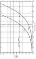
LED 들 간의 제조상의 차이(manufacturing variations)로 인하여, 특정의 전류 레벨을 유지하기 위하여 필요한 각 LED 스트링에 대한 전압 강하(voltage drop)는 상당히 달라진다. 도 1의 VI 곡선은 2개의 상이한 LED들 (LED1 및 LED2)에 대하여 전압과 전류 간의 기하급수적인 관계(exponential relationships)를 나타낸다. LED1 및 LED2이 동일한 양의 피크 전류(peak current)를 제공하기 위하여, LED1은 약 3.06 볼트(volts)의 순방향 전압 강하(forward voltage drop)에서 동작하여야 하는 반면에, LED2는 약 3.26 볼트(volts)의 순방향 전압 강하에서 동작하여야 한다. 제1 LED 스트링에서 LED1의 특성을 가진 10개의 LED 들이 있다고 가정하면, 상기 스트링에 대하여 30.6 볼트의 강하가 있다. 제2 LED 스트링(102)에서 LED2의 특성을 가진 10개의 LED 들이 있다고 가정하면, 제2 LED 스트링에 대하여 32.6 볼트의 강하가 있다. 2볼트의 차는 제2 스트링을 구동하는 회로에 의해 소멸되어, 양 스트링들은 40mA의 동일한 피크 전류에서 동작한다. Due to manufacturing variations between the LEDs, the voltage drop for each LED string needed to maintain a certain current level is significantly different. The VI curves in FIG. 1 represent the exponential relationships between voltage and current for two different LEDs (LED1 and LED2). LED1 should operate at a forward voltage drop of approximately 3.06 volts while LED2 should operate at approximately 3.26 volts so that LED1 and LED2 provide the same amount of peak current, Of the forward voltage drop. Assuming that there are 10 LEDs with the characteristics of LED 1 in the first LED string, there is a 30.6 volt drop for the string. Assuming that there are 10 LEDs with the characteristics of LED2 in the second LED string 102, there is a 32.6 volt drop for the second LED string. The 2 volt of the car is dissipated by the circuit driving the second string so that both strings operate at the same peak current of 40 mA.
상이한 LED들의 예측불가한(unpredictable) VI 특성은 전력 효율적인 방법으로 상이한 LED 스트링들을 동작시키는 것을 어렵게 하는 반면에, 상기 LED 스트링들의 휘도에 대한 정확한 제어를 여전히 지속시킨다. 이러한 어려움들을 다루기 위하여 상이한 기법들이 개발되어 왔으나, 기존의 많은 해결책들은 비효율적이거나 또는 LED 스트링들을 통한 전류를 조절하기 위하여 사용되는 부품들의 비용을 상당히 증가시키는 회로의 추가를 필요로 한다.The unpredictable VI characteristics of the different LEDs make it difficult to operate different LED strings in a power efficient manner while still maintaining accurate control over the brightness of the LED strings. Different techniques have been developed to deal with these difficulties, but many existing solutions require the addition of circuitry that is inefficient or significantly increases the cost of components used to regulate current through the LED strings.
스위칭 전력 변환 장치 콘트롤러는 전력 변환 장치의 차후의(이어지는) 스위칭 사이클(subsequent switching cycle)에 대한 예측 부하(predicted load)를 추정하는 예측 피드 순방향 제어 메커니즘(predictive feed forward control mechanism)을 이용하여 전력 변환 장치의 스위칭을 제어한다. 일 실시예에서는, 예측 부하 신호(predicted load signal)가 스위칭 전력 변환 장치의 제1 스위칭 사이클 동안에 수신된다. 예측 부하 신호는 스위칭 전력 변환 장치의 제1 스위칭 사이클에 이어지는(subsequent to) 제2 스위칭 사이클 동안에 하나 이상의 LED 스트링들의 예측 부하를 나타낸다. 듀티 사이클(duty cycle)은 제2 스위칭 사이클 동안에 스위칭 전력 변환 장치를 구동하기 위하여, 예측 부하에 기반하여 결정된다. 스위칭 전력 변환 장치는 하나 이상의 LED 스트링들에 전력을 공급하는 조절된 출력 전압(regulated output voltage)을 달성하기 위하여 상기 듀티 사이클을 사용하여 제2 스위칭 사이클 동안에제 제어된다.The switching power converter controller uses a predictive feed forward control mechanism that estimates a predicted load for a subsequent switching cycle of the power converter, And controls the switching of the device. In one embodiment, a predicted load signal is received during the first switching cycle of the switching power converter. The predicted load signal represents a predicted load of one or more LED strings during a second switching cycle subsequent to a first switching cycle of the switching power converter. The duty cycle is determined based on the predicted load to drive the switching power converter during the second switching cycle. The switching power converter is controlled during the second switching cycle using the duty cycle to achieve a regulated output voltage that powers one or more LED strings.
실시예들은 하나 이상의 LED 스트링들을 구동하는 시스템을 포함한다. 시스템은 LED 콘트롤러 및 전력 변환 콘트롤러(power conversion controller)를 포함한다. LED 콘트롤러는 하나 이상의 LED들을 구동하는 휘도 세팅(brightness setting)을 수신하기 위하여 연결된다(coupled). LED 콘트롤러는 휘도 세팅에서 동작하는 하나 이상의 LED 스트링들의 예측 부하를 나타내는 예측 부하 신호를 생성한다. 전력 변환 콘트롤러는 스위칭 전력 변환 장치의 제1 스위칭 사이클 동안에 LED 콘트롤러로부터 예측 부하 신호를 수신하기 위하여 연결된다. 전력 변환 콘트롤러는 예측 부하 신호에 기초하여 제어 신호를 생성한다. 제어 신호는 제1 스위칭 사이클에 이어지는 제2 스위칭 사이클 동안 스위칭 전력 변환 장치의 스위칭을 제어하기 위한 듀티 사이클을 가진다. 스위칭 전력 변환 장치는 하나 이상의 LED 스트링들에 전력을 공급한다.Embodiments include a system for driving one or more LED strings. The system includes an LED controller and a power conversion controller. The LED controller is coupled to receive a brightness setting driving one or more LEDs. The LED controller generates a predicted load signal indicative of a predicted load of one or more LED strings operating in the luminance setting. The power conversion controller is coupled to receive a predicted load signal from the LED controller during a first switching cycle of the switching power converter. The power conversion controller generates a control signal based on the predicted load signal. The control signal has a duty cycle for controlling switching of the switching power converter during a second switching cycle following the first switching cycle. The switching power converter supplies power to one or more LED strings.
유익하게(beneficially), 전력 변환 콘트롤러는 피드백 조절(feedback regulation)에 전적으로 의지하기 보다는 스위칭 전력 변환 장치의 스위칭을 제어하기 위하여 예측 부하 신호를 이용한다. 이는 LED 스트링들의 부하 상태(load conditions)들을 변화시키도록 조정할 때, 스위칭 전력 변환 장치의 동적 응답(dynamic response)을 개선시킨다. 개선된 동적 응답은 과도 상태(transient conditions) 동안에 조절 전압(regulation voltage) 아래로 출력 전압이 강하될 때 일어날 수도 있는 깜빡거림(flickering)과 같은 성능 문제를 감소 또는 제거한다. 또한, 개선된 동적 응답은 과도 상태 동안에 조절 전압 위로 출력 전압이 상승할 때 일어날 수도 있는 원하지 않는 전력 낭비(power dissipation)를 감소 또는 제거한다.Beneficially, the power conversion controller uses the predicted load signal to control the switching of the switching power converter rather than relying entirely on feedback regulation. This improves the dynamic response of the switching power converter when adjusting to vary the load conditions of the LED strings. The improved dynamic response reduces or eliminates performance problems such as flickering that may occur when the output voltage falls below a regulation voltage during transient conditions. In addition, the improved dynamic response reduces or eliminates unwanted power dissipation that may occur when the output voltage rises above the regulated voltage during transient conditions.
본 명세서에서 상술되는 특징과 잇점들은 모두 포괄되지 못하고, 특히 많은 부가적인 특징과 잇점들이 도면, 상세한 설명, 및 청구항을 통하여 본 발명의 기술분야에 종사하는 사람들에게 자명하다. 또한, 본 명세서의 용어들은 주로 가독성(readability) 및 교육 목적들을 위하여 선택되었고, 발명의 주제를 제한하기 위하여 선택된 것은 아니다.The features and advantages described in the specification are not all encompassed, and in particular, many additional features and advantages are apparent to those skilled in the art through the drawings, detailed description, and claims. In addition, the terms herein have been chosen primarily for readability and educational purposes, and are not chosen to limit the subject matter of the invention.
본 발명의 실시예들은 첨부된 도면들과 연관되어 다음의 상세한 설명을 고려하여 쉽게 이해될 수 있다.
도 1은 순방향 바이어스된(forward biased) LED들의 I-V 커브들에 대한 제조상의 차이의 효과를 도시한 그래프이다.
도 2는 다수의 LED 스트링들을 구동하는 고 레벨 시스템을 도시한 것이다.
도 3a는 스위칭 변환 장치의 실시예에 대한 회로 블록도를 도시한 것이다.
도 3b는 불연속 도통 모드 (DCM: Discontinuous Condution Mode)에서 동작하는 스위칭 변환 장치와 연관된 파형을 도시한 것이다.
도 4는 LED 콘트롤러에 의하여 제어되는 LED 드라이버의 실시예를 도시한 회로 블록도이다.
도 5는 전형적인 LED 에 대하여, 전기적 전류와 광학적 휘도 사이의 전형적 비선형 전달 함수를 도시한 그래프이다.
도 6은 전형적인 LED 에 대하여, 광속 밀도(luminous flux density)의 전형적 온도 감쇄(de-rating)를 접합 온도(junction temperature)의 함수로서 도시한 그래프이다.BRIEF DESCRIPTION OF THE DRAWINGS Embodiments of the present invention can be readily understood by considering the following detailed description in conjunction with the accompanying drawings.
Figure 1 is a graph illustrating the effect of manufacturing differences on IV curves of forward biased LEDs.
Figure 2 shows a high level system driving multiple LED strings.
Figure 3A shows a circuit block diagram for an embodiment of a switching transducer.
Figure 3B illustrates waveforms associated with a switching transducer operating in a discontinuous conduction mode (DCM).
4 is a circuit block diagram illustrating an embodiment of an LED driver controlled by an LED controller.
5 is a graph illustrating a typical nonlinear transfer function between electrical current and optical brightness for a typical LED.
Figure 6 is a graph illustrating the typical temperature de-rating of a luminous flux density as a function of junction temperature for a typical LED.
도면들과 이하의 기재 내용들은 본 발명의 바람직한 실시예들의 예시로서만 관련된다. 이하의 논의로부터, 여기에 개시되는 구조 및 방법의 또다른 실시예들이 청구된 발명의 원리에 벗어남이 없이 채택될 수 있는 자명한 실시예로 쉽게 인식될 수 있음은 주목해야 한다.The drawings and the following description are relevant only as examples of preferred embodiments of the present invention. It should be noted from the following discussion that other embodiments of the structures and methods disclosed herein may be readily recognized as obvious embodiments that may be employed without departing from the principles of the claimed invention.
본 발명의 여러 실시예들, 일례로 첨부된 도면들에서 도시된 예들이 상세하게 참조될 것이다. 실시가능한 유사한 참조번호들이 도면들 어디서든지 사용되고 유사한 기능을 나타낸다. 도면들은 도시의 목적으로만 본 발명의 실시예들을 기술한다. 본 발명의 기술 분야에 종사하는 사람들은 이하의 기재 내용으로부터 구조 및 방법의 다른 실시예들이 이하 기술된 발명의 원리에 벗어남이 없이 채택될 수 있음을 쉽게 인식할 수 있다.
Reference will now be made in detail to various embodiments of the invention, examples of which are illustrated in the accompanying drawings, by way of example. Similar reference numbers that may be employed are used anywhere in the figures and indicate similar functions. The drawings illustrate embodiments of the invention only for purposes of illustration. Those skilled in the art will readily appreciate that other embodiments of the structures and methods may be adopted without departing from the principles of the invention described below.
시스템 아키텍쳐 (System Architecture)System Architecture
도 2는 다수의 LED 스트링(225)들을 구하는 시스템의 일 실시예를 도시한 것이다. 시스템은 LED 드라이버(230), LED 콘트롤러(240), 비디오 콘트롤러(250), 전력 변환 장치 콘트롤러(210), 및 스위칭 전력 변환 장치(220)를 포함한다. 다른 실시예들은 상이하거나 또는 추가 컴포넌트들을 포함할 수 있다.FIG. 2 illustrates one embodiment of a system for obtaining a plurality of
비디오 콘트롤러(250)는, 예를 들어, LCD 디스플레이가 이미지를 형성하도록 제어하는 장치일 수 있다. 비디오 콘트롤러(250)는 LCD 디스플레이에 대한 바람직한 백라이트 요건(backlighting requirements)들을 결정하고, 제어 신호(207)를 통하여 LED 콘트롤러(240)로 전송한다. 예를 들어, 일 실시예에서는, 제어 신호(207)가 LED 스트링들(225)에 대한 휘도 세팅과 LED 스트링들(225)에 대한 미리 결정된 기준치 전류(predetermined baseline current)를 포함한다. 일반적으로, 비디오 콘트롤러(250)는 비디오 콘트롤러(250)의 수직 동기(Vsync) 사이클 당 한 번씩 제어 신호(207)를 업데이트한다. 2개의 별개의 장치들(separate devices)로 보여짐에도 불구하고, 일 실시예에서, 비디오 콘트롤러(250) 및 LED 콘트롤러(240)는 동일한 집적 회로 장치의 별개의 컴포넌트들 또는 동일한 집적 회로 장치상에서 실행되는 펌웨어 내의 별개의 스레드(thread)일 수 있다.The video controller 250 may be, for example, a device that controls the LCD display to form an image. The video controller 250 determines the desired backlighting requirements for the LCD display and transmits it to the
LED 콘트롤러(240)는 제어 신호(207)를 비디오 콘트롤러(250)로부터 수신하고, 비디오 콘트롤러(250)에 의해 명시된(specified) 바람직한 휘도를 달성하기 위하여 LED 스트링들(225)를 구동하기 위한 전류 레벨들(current levels) 및 듀티 사이클들(예를 들어, 오/오픈 시간들)을 결정한다. 프로그램된(programmed) 전류 레벨들 및 듀티 사이클들은 신호(235)를 통하여 LED 드라이버(230)로 전달되고(communicated), 이것은 전달된 세팅들에 따라서 LED 스트링들(225)을 구동한다. LED 콘트롤러(240)는 상이한 LED 스트링들(225)에 대하여 상이한 세팅들을 명시할 수 있고, 따라서 LED 드라이버(230)가 상이한 LED 스트링들(225)에 대하여 상이한 휘도값들을 달성하도록 한다.The
LED 콘트롤러(240) 및 LED 드라이버(230)는 통신 링크(communication link)(235)를 통하여 서로 통신한다. 일 실시예에서, 통신 링크(235)는 정보를 실어 나르기 위하여 2개 이상의 집적 회로 장치를 연결하는 직렬 또는 병렬 링크(serial or parallel link)를 나타낼 수 있다. 예를 들어, 통신 링크(235)는 직렬 프로토콜 인터페이스(SPI), I2C 버스(inter-integrated circut bus) 등일 수 있다. 통신 링크(235)는 각각의 링크가 한가지 타입의 정보(예를 들어, 듀티 사이클 세팅, 프로그램된 전류 레벨, 또는 조절 정보)를 전용해서 실어 나르는 개별적인 통신 링크들의 집합(aggregation of individual communication links)을 역시 나타낼 수 있다.The
LED 콘트롤러(240) 및 LED 드라이버(230)는 다수의 LED 스트링들(225)을 효율적으로 구동하는 기법으로서 적응 스위칭(adaptive switching)을 이용하여 동작할 수 있다. 예를 들어, 일 실시예에서, LED 콘트롤러(240)는 LED 채널(225)을 통한 전류 흐름이 조절되고 있거나 또는 조절을 벗어나고 있다(in or out of regulation)는 것을 나타내는 조절 정보(regulation informatoin)를 통신 링크(235)를 통하여 LED 드라이버(230)로부터 수신한다. 캘리브레이션 과정(calibration process) 동안, LED 콘트롤러(240)는 각각의 LED 채널들(225)에 대한 프로그램된 전류 값을 결정하기 위하여 조절 정보를 사용한다. 일 실시예에서, 프로그램된 전류는 기준치 전류에 대하여 가능한 전류 값들의 한정된 셋(limited set)으로부터 선택된다. 각각의 LED 채널(225)은 상이한 프로그램된 전류 값을 가질 수 있고, 이것은 상이한 LED 스트링들(225)의 변화하는 I-V 특성들에 기초하여 채널에 대한 전력 효율을 최적화하도록 설정된다.The
미리 결정된 기준치 전류 세팅, 휘도 세팅, 및 프로그램된 전류 레벨들을 이용하여, LED 콘트롤러(240)는 LED 채널들(225)에 대한 듀티 사이클들을 계산한다. 각각의 LED 채널(225)의 프로그램된 전류 값들 간의 차이(variation)를 보상하고, 각각의 LED 채널(225)의 상대적 휘도에 대한 제어를 유지하기 위하여, 상이한 듀티 사이클들이 상이한 채널들에 대하여 프로그램될 수 있다. 예를 들어, 더 낮은 피크 전류 값들(lower peak current values)을 가진 LED 스트링들(225)은 더 높은 듀티 사이클들을 가질 수 있다. 적응 스위칭을 이용한, LED 드라이버(230) 및 LED 콘트롤러(240)의 동작에 대한 상세한 내용들이 도 4를 참조하여 이하에 제공된다.Using the predetermined reference current setting, the luminance setting, and the programmed current levels, the
LED 콘트롤러(240)는 각각의 LED 스트링(225)에 대하여 알려진 프로그램된 전류 레벨들 및 듀티 사이클들에 기초하여 예측 부하 신호(predictive load signal)(216)를 역시 생성하고, 전력 변환 장치 콘트롤러(210)로 예측 부하 신호(216)를 출력한다. 예측 부하 신호(216)는 스위칭 전력 변환 장치(220)의 이어지는 스위칭 사이클들에서 Vboost를 제어하기 위하여 유도될 수 있다. 일 실시예에서, 예를 들어, 예측 부하 신호(216)는 스위칭 전력 변환 장치(220)의 스위칭 사이클의 과정에 대하여 LED 스트링들(225)을 통한 누적 평균 전류(average cumulative current)를 나타내거나 또는 평균 누적 전류가 유도될 수 있는 정보이다. 또달리, 예측 부하 신호(216)는 미리 결정된 시간 주기 동안 LED 스트링들(225)에 의해 소비될 추정 전력(estimated power) 또는 추정 전력이 유도될 수 있는 다른 정보일 수 있다. 예측 부하 신호(216)는 이하에서 보다 상세히 기술될 부하 변화(load variations)를 보상하기 위하여, 전력 변환 장치 콘트롤러(210)가 보다 효율적으로 스위칭 전력 변환 장치(220)의 출력을 조정할 수 있도록 한다.The
스위칭 전력 변환 장치(220)는 입력 전압 Vin을 조절하고, 공통 전압 Vboost(245)를 다수의 LED 스트링들(225)에 제공한다. 피드백 경로(feedback path)상에서, 전력 변환 장치 콘트롤러(210)는 스위칭 전력 변환 장치(220)의 출력 전압 Vboost(245)을 나타내는 피드백 전압(VFB)(214)을 스위칭 전력 변환 장치(220)로부터 감지하고, Vboost(245)를 바람직한 조절 전압(regulation voltage)에서 유지하기 위하여 스위칭 전력 변환 장치(220)의 스위칭을 제어하는 제언 신호(212)를 제공한다. 예를 들어, 일 실시예에서, 제어 신호(212)는 스위칭 전력 변환 장치(220)의 스위칭을 제어하는 펄스 폭 변조(PWM: Pulse Width Modulation) 신호를 포함한다. 또달리, 제어 신호(212)는 펄스 주파수 변조(PFM: Pulse Frequency Modulation) 신호를 포함한다. 따라서, 만약 Vboost(245)가 조절 전압 이하로 떨어지기 시작하면(왜냐하면, 예를 들어, LED 스트링들(225)의 부하 수요(load demand)가 증가하였기 때문에), 전력 변환 장치 콘트롤러(210)는 피드백 신호(214)를 통하여 Vboost(245)의 전압 강하를 감지하고, 제어 신호(212)의 듀티 사이클을 증가시키고, Vboost(245)에서의 강하에 대응한다(counteracting). 유사하게, Vboost(245)가 조절 전압 이상으로 상승하면(왜냐하면, 예를 들어, LED 스트링들(225)의 부하 수요(load demand)가 감소하였기 때문에), 전력 변환 장치 콘트롤러(210)는 피드백 신호(214)를 통하여 전압 상승(voltage rise)을 감지하고, 제어 신호(212)의 듀티 사이클을 감소시키고, Vboost(245)에서의 상승에 대응한다(counteracting).The switching
앞서 논의된 바와 같이, LED 스트링들(225)의 프로그램된 전류 및 듀티 사이클들(및 전체 부하 조건들)은 비디오 콘트롤러(250)에 의해 설정된 휘도 세팅들에 따라서 사이클 당 변화할 수 있다. 예를 들어, 일 실시예에서, 프로그램된 전류 및 듀티 사이클들은 비디오 콘트롤러(250)의 Vsync 사이클 당 한 번씩 업데이트된다. 상기한 전력 변환 장치 콘트롤러(210)의 피드백 제어 메커니즘이 변화하는 부하 수요로부터 발생되는 Vboost(245)의 상승 또는 강하에 대응하기 위하여 작동하는 동안에, 동적 부하 응답 시간(dynamic load response time)이 피드 순방향 예측 부하 신호(216)에 기초하여 스위칭 전력 변환 장치(220)의 듀티 사이클을 더 조정함으로써 향상될 수 있다. 예측 부하 신호(216)는 전력 변환 장치 콘트롤러(210)에 스위칭 전력 변환 장치(220)의 이어지는 스위칭 사이클 동안에 기대 부하(expected load)를 추정하는 사전 정보(advance information)를 공급한다. 따라서, 전력 변환 장치 콘트롤러(210)는 Vboost(245)(피드백 전압(214)을 통하여 감지되는)의 상승 또는 하강을 통하여 발견되는 부하 변화를 기다리지 않고도, 변화하는 부하를 예측하여 제어 신호(212)를 조정할 수 있다. 결과로, 동적 부하에 대한 루프 응답(loop response)은 상당히 개선될 수 있다.As discussed above, the programmed currents and duty cycles (and overall load conditions) of the LED strings 225 may vary from cycle to cycle, depending on the luminance settings set by the video controller 250. For example, in one embodiment, the programmed current and duty cycles are updated once per Vsync cycle of the video controller 250. While the feedback control mechanism of the
일 실시예에서, LED 콘트롤러는 조정된 휘도 세팅들이 비디오 콘트롤러(250)로부터 수신될 때마다 예측 부하 신호(216)를 업데이트한다(예를 들어, Vsync 사이클 당 한 번씩). 또달리, LED 콘트롤러(240)는 스위칭 전력 변환 장치(220)의 각 스위칭 사이클당, 두 개의 스위칭 사이틀 당 한번씩, 세 개의 스위치 사이클 당 한번씩 등 이어지는 사이클에 상응하는 예측 정보를 가지고 예측 부하 신호를 업데이트할 수 있다. 따라서, 예를 들어, 제1 스위칭 사이클 동안에 수신된 예측 부하 신호(216)는 제1 스위칭 사이클 후에 언젠가 제2 스위칭 사이클 동안에 스위칭 전력 변환 장치(220)를 제어하기 위한 정보를 제공한다. 예측 부하 신호(216)를 결정하기 위한 프로세스의 일례가 도 3a - 도3b를 참조하여 이하에서 기재된다.In one embodiment, the LED controller updates the predicted load signal 216 (e.g., once per Vsync cycle) every time the adjusted luminance settings are received from the video controller 250. Alternatively, the
일 실시예에서, 예측 부하 신호(216)는 제1 및 제2 차수 제어(first and second order control)를 가진 시스템과 결합하여 사용될 수 있다. 예를 들어, 동작의 스캔 모드(scan mode)를 사용하는 텔레비젼 백라이팅 시스템에서는, 제1 차수 휘도 제어는 PWM 듀티 사이클에 의해 달성되고, 제2 차수 휘도 제어는 더 낮은 주파수의 스캔 듀티 사이클에 기초하여 달성된다. 제1 및 제2 차수 제어들이 삽입될 때에만, 전류는 LED 스트링들(225)을 통하여 전도된다(conducted). 예를 들어, 120Hz의 Vsync 주기 및 2.4 KHz의 PWM 주파수를 가정하자. PWM 듀티 사이클이 50%로 설정되고, 스캔 듀티 사이클이 100%로 초기에 설정된다면, 이는 Vsync 주기 동안에 대해, 50%의 듀티 사이클의 20개의 PWM 펄스들을 초래하고, 50%의 프로그램된 값의 평균 전류를 초래한다. 다음으로, 만약 스캔 듀티(scan duty)가 이어지는 Vsync 주기에 대하여 50%로 조정된다면, Vsync 주기 동안에 대해, 50%의 듀티 사이클의 10개의 PWM 펄스들을 초래하고, 단지 25%의 프로그램된 값의 평균 전류를 초래한다. 따라서, 일 실시예에서, 예측 부하 신호(216)는 여기서 기술되는 동일한 원칙에 따라서, 제1 및 제2(및/또는 심지어 더 높은 차수) 휘도 제어에 기초하여 예측 정보를 포함한다(incorporate).In one embodiment, the predicted
예측 순방향 아키텍쳐(predictive forward architecture)에 의해 달성되는, 개선된 동적 부하 응답은 몇 가지 이득이 있다. 첫째, Vboost(245)가 증가된 부하 수요에 기인하여 조절 전압 이하로 하강할 때 발생할 수 있는 LED 깜박거림(flickering)을, 개선된 부하 응답은 감소 또는 예방할 수 있다. 둘째, Vboost(245)가 감소된 부하 수요에 기인하여 조절 전압 이상으로 상승할 때 발생할 수 있는 원치 않는 전력 낭비를, 개선된 부하 응답은 감소 또는 제거할 수 있다. 셋째, 개선된 부하 응답이, 감소된 출력 커패시턴스(output capacitance)와 연관된 Vboost(245)의 더 큰 전압 스윙(voltage swings)들을 보상하기 때문에, 더 작은 출력 캐패시터(output capacitor)가 성능의 희생 없이도 스위칭 전력 변환 장치(220)에 사용될 수 있다. 승압 변환 장치(boost converter)(220)의 더 작은 출력 커패시턴스를 이용하는 것이 종종 바람직하다. 왜냐하면, 그것이 재료 비용을 낮추고 발전소의 대역폭을 증가시켜서 루프 제어가 조절을 유지하는데 훨씬 더 많은 일들을 수행하도록 하기 때문이다.The improved dynamic load response, achieved by a predictive forward architecture, has several benefits. First, LED flickering, which can occur when
일 실시예에서, LED 콘트롤러(240) 및 LED 드라이버(230)는 별개의 집적 회로 장치이다(예를 들어, 분리되어 있고 다르다). 다시 말해서, LED 콘트롤러(240)는 LED 드라이버(230)와 동일한 집적 회로 장치의 일부가 아니다. 또달리, LED 콘트롤러(240) 및 LED 드라이버(230)는 동일한 집적 회로 내에 집적될 수 있다. 또한, 하나의 실시예에서, LED 콘트롤러(240) 및 전력 변환 장치 콘트롤러(210)는 동일 집적 회로 장치 내에 포함된다. 이 실시예에서, 전력 변환 장치 콘트롤러(210) 및 LED 콘트롤러(240)에 의해 수행되는 다양한 연산들에 대한 연산 프로세싱 유닛(arithmetic processing unit)은 공유될 수 있어서, 시스템 전체 비용을 감소시킬 수 있다.
In one embodiment,
전력 변환 콘트롤러 및 스위칭 변환 장치의 동작Operation of power conversion controller and switching converter
도 3a는 스위칭 전력 변환 장치(220)으로 사용될 수 있는 부스트 변환 장치(320)의 아키텍쳐의 일례를 도시한다. 부스트 변환 장치(320)에서는, 스위칭 트랜지스터(Q1)가 턴온(turn-on)될 때, 에너지가 인덕터 L에 저장된다. 스위칭 트랜지스터 Q1은 턴오프될 때, 에너지가 다이오드(D1)을 통하여 커패시터 C1으로 전달되고, 출력 전압 Vo로 나타난다. 저항 R1 및 R2를 포함하는 전압 분배기(voltage divider)가 전압 Vo를 나타내는 피드백 감지된 전압 VFB를 생성하기 위하여 연결된다(coupled). VFB는 피드백 전압(214)으로 사용될 수 있고, Vo는 Vboost를 제공하도록 연결될 수 있다.3A shows an example of the architecture of the
도 3b는 불연속 전도 모드(DCM: Discontinuous Condution Mode)에서 동작할때, 부스트 변환 장치 및 부스트 변환 장치(320)를 통하는 인덕터 전류 IL를 구동하는 PWM 신호(312)에 대한 파형 다이어그램을 예시한 것이다. 시간 주기(301) 동안에, PWM 신호(312)가 삽입되어, 스위칭 트랜지스터(Q1)은 턴온된다. 인덕터 L이 충전됨에 따라서, 인덕터 전류(IL)가 ml 비율로 증가한다. 시간 주기(301)는 충전 시간(charge time)으로 알려지고 d1ts로 주어진다. 단, d1은 PWM 신호(312)의 듀티 사이클이고, Ts는 PWM 신호(312)의 주기를 나타낸다. 시간 주기(303) 동안, PWM 신호(312)는 로우(low)이고, 스위칭 트랜지스터 Q1은 턴 오프된다. 인덕터 L이 방전됨(discharge)에 따라서, 인덕터 전류(IL)가 m2 비율로 감소하고, 따라서 다이오드 전류(ID)를 공급하고, 커패시터 C1에 출력 전압 VO를 생성한다. 시간 주기(303)는 방전 시간(charge time)으로 알려지고 d2ts로 주어지는데, 여기서 d2는 인덕터 L이 방전하고 있는 동안, 주기 Ts의 백분율(percentage)이다. 시간 주기(305) 동안, 인덕터 L이 완전히 방전되기 때문에, 인덕터 전류 IL이 거의 0이다. 시간 주기(305)는 불감 시간(dead time)으로 알려지고, d3ts로 주어지는데, 여기서 d3는 방전 사이클 및 다음 PWM 사이클의 시작 이전에 인덕터 전류가 0일 때, 주기 Ts의 백분율(percentage)이다.3B illustrates a waveform diagram for the PWM signal 312 driving the inductor current IL through the boost converter and the
도 3a 및 3b로부터 보는 바와 같이, 인덕터 L을 통한 최대 전류 IMAX가 다음과 같이 주어진다.3A and 3B, the maximum current IMAX through the inductor L is given by:

충전 시간(301) 동안에, Q1은 온(on)이고, 인덕터 L에 대한 전압은 Vin이다. 따라서, m1 은 다음과 같이 주어진다.During the charging time (301), Q1 is turned on (on), and the voltage across the inductor Lin V. Therefore, m1 is given by

방전 시간(303) 동안에, Q1은 오프(off)이고, 인덕터 L에 대한 전압은 VO- Vin이다. 따라서, m2 는 다음과 같이 주어진다.A Vin - during a discharge time (303), Q1 is the voltage on and off (off), the inductor L is VO. Thus, m2 is given by

d2에 대하여 계산하고, m1 및 m2 에 대하여 치환하면 다음과 같다.d2 , and substituting for m1 and m2 , the following is obtained.

주기 Ts에 대하여 평균 다이오드 출력 전류 <ID>Ts는 다음과 같이 주어진다.The average diode output current < ID >Ts for the period Ts is given by:

d1에 대하여 풀면 다음과 같다.For d1 , the solution is as follows.

따라서, 수식 (6)에 보는 바와 같이, 전력 변환 장치 콘트롤러(210)의 적절한 듀티 사이클 d1은 입력 전압 Vin, 인덕턴스(L), PWM 주기(Ts), 출력 전압(Vo), 및 PWM 사이클 <ID>Ts당 평균 다이오드 전류에 기초하여 결정될 수 있다. 여기서, Vin 및 Vo는 피드백 연결(233, 214)을 통하여 전력 변환 장치 콘트롤러(210)에 의해 모니터링된다. PWM 주기 Ts는 전력 변환 장치 콘트롤러(210)에 의해 설정되고, 전형적으로 변함없는 스루풋 동작(constant throughput operation)으로 유지되기 때문에, 알려진다. 인덕턴스 L 은 알 수 있거나, 또는 스타트업 캘리브레이션 시퀀스(startup calibration sequence) 동안 측정될 수 있다. 평균 다이오드 전류 <ID>Ts는 스위칭 주기 Ts 동안에, LED 스트링들을 통한 누적 평균 전류와 동등하다. 이러한 평균 전류 <ID>Ts는 프로그램된 전류들 및 듀티 사이클들로부터 LED 콘트롤러(240)에 의해 결정될 수 있고, 예측 부하 신호(216)를 통하여 전력 변환 콘트롤러(210)로 제공된다. 예를 들어, 평균 전류 <ID>Ts는 다음과 같이 결정될 수 있다.Thus, as shown in equation (6), the proper duty cycle d1 of the

여기서, dLEDn는 스위칭 주기 Ts 동안의 LED 스트링 n에 대하여 프로그램된 듀티 사이클이고, iLEDn 은 N개의 LED 스트링들을 구동하는 LED 드라이버(230)에 대한 스위칭 주기 Ts 동안의 LED 스트링 n을 통하여 프로그램된 전류이다.Where dLEDn is the duty cycle programmed for the LED string n during the switching period Ts and iLEDn is the duty cycle programmed through the LED string n during the switching period Ts for the LED driver 230 driving the N LED strings Current.
LED 콘트롤러(240)가 프로그램된 전류, 및 스위칭 전력 변환 장치(220)의 이어지는 듀티 사이클에 대한 듀티 사이클들을 미리 획득하기 때문에, LED 콘트롤러(240)는 이어지는 듀티 사이클에 대한 평균 다이오드 전류 <ID>Ts를 역시 미리 계산하고, 예측 부하 신호(216) 내에 이 정보를 제공할 수 있다. 따라서, 전력 변환 장치 콘트롤러(210)는 미래의 듀티 사이클에 대한 적절한 제어 세팅들을 듀티 사이클에 앞서 예측할 수 있고, 감지된 피드백 전압 VFB에 전적으로 의지하지 않아도 된다.The
또다른 실시예에서, 다른 형태의 스위칭 전력 변환 장치(220)가 사용될 수 있다. 예를 들어, 스위칭 전력 변환 장치(220)는 벅 변환 장치(buck converter), 벅-부스트 변환 장치, 플라이백 변환 장치(flyback converter) 또는 다른 형태의 스위칭 변환 장치를 포함할 수 있다. 더우기, 전력 변환 장치 콘트롤러(210)는 앞서 서술한 불연속 전도 모드 또는 연속 전도 모드를 포함하는 다양한 동작 모드들에서 스위칭 전력 변환 장치(220)를 제어할 수 있다. 추가적으로, 예를 들어, 앞서 설명한 펄스 폭 변조(pulse width modulation) 또는 펄스 주파수 변조(pulse frequency modulation)를 포함하는 상이한 제어 메커니즘이 스위칭 전력 변환 장치(220)를 제어하는데 사용될 수 있다. 비록 앞서 설명한 정확한 계산은 사용되는 변환 장치, 동작 모드 및 제어 메커니즘의 타입에 따라서 변하지만, 일반적 원칙이 다양하게 넓은 시스템들에 적용될 수 있다.
In another embodiment, other types of switching
LED 드라이버 (LED Driver)LED Driver (LED Driver)
도 4는 LED 콘트롤러(240)에 의해서 제어되는 LED 드라이버(230)의 실시예에 대한 회로 블록도이다. 각각의 LED 채널에서, LED 스트링(225)는 LED 채널(225)의 LED들의 온 타임(on-times) 및 오프 타임(off-times)들을 제어하기 위하여 PWM 스위치 QP와 직렬로 연결되어 있다. LED 스트링(225) 및 PWM 스위치 QP와 LED 채널(225)를 통한 전류를 제어하기 위하여 강하 레귤레이터(LDO: low dropout regulator)와 직렬로 역시 연결될 수 있다. LDO(404)는 LED 스트링(225)에서의 피크 전류가 고정된 레벨로 조절되도록 보장한다. LDO(404)는 LED 스트링들(225)의 휘도(luminance)에 대한 Vboost 전압으로부터의 부스트 전압 리플(voltage ripple)의 효과를 감소시키기 위하여 자연의 전력 전원 제거(power supply rejection)를 역시 제공한다. 각각의 LED 채널에서, LDO(404)는 LED 채널(225)을 통한 전류, PWM 듀티 사이클, 및 LDO(404)에서의 전압 강하(voltage drop)의 곱(product)에 비례하는 전력을 소비(dissipate)한다.4 is a circuit block diagram of an embodiment of an LED driver 230 that is controlled by an
LED 드라이버(230)는, LED 콘트롤러(240)로부터 수신된 듀티 사이클 세팅들(494)에 따라서 제어 신호들(408)을 통하여 PWM 스위치 QP를 제어함으로써, 각각의 LED 채널의 밝기를 독립적으로 제어하는 휘도 콘트롤러(410)(luminance controller)를 포함한다. 듀티 사이클 세팅들(494)은 PWM 스위치 QP의 온 및 오프 타임들(on and off times), 예를 들어 시간의 백분율(percentage of time)(예, 40%, 60%), 또는 개별적인 듀티 사이클 온 타임 및 듀티 사이클 주기를 설정하는데 이용될 수 있는 정보를 포함한다. 휘도 콘트롤러(410)는 제어 신호들(409)을 통하여 LDO들(404)을 제어하고, LED 콘트롤러로부터 수신된 프로그램된 전류 레벨들(492)에 따라서 디지털-아날로그 변환 장치들(DACs: digital-to-analog converters)(407)을 역시 제어한다.The LED driver 230 controls the PWM switch QP through the control signals 408 in accordance with the duty cycle settings 494 received from the
부가적으로, LDO(404)는, LDO(404)가 멀티플렉서(multiplexer)(411)를 통하여 휘도 콘트롤러(410)에 대하여 조절되지 않는지를 나타내는 조절 피드백 신호(regulation feedback signal)(415)를 출력한다. 이러한 조절 피드백(490)은 LED 콘트롤러(240)로 전달되고, LED 콘트롤러(240)는 캘리브레이션 동안에 LED 채널들을 통하여 프로그램된 전류 레벨들(492)을 설정하기 위하여 조절 정보(490)를 사용하게 되는데, 이하 보다 자세히 상술된다.In addition, the
비록 도 4는 단지 2개의 LED 채널들을 예시하고 있지만, LED 드라이버(230)는 어떠한 개수의 LED 스트링들(225)에 대한 회로도 포함할 수 있다. LED 드라이버(230)의 다른 실시예들이, "다중 피드백 루프들을 가진 LED 드라이버"라는 발명의 명칭을 가진 미국 특허출원공보 No.2009/0322234 및, 2009년 9월 11일에 "적응 스위치 모드 LED 드라이버"라는 발명의 명칭으로 출원된 미국 출원번호 No. 12/558,275에 나와 있는데, 그 내용들이 전체로서 합쳐져서 참조된다.Although FIG. 4 illustrates only two LED channels, the LED driver 230 may include circuitry for any number of LED strings 225. Other embodiments of the LED driver 230 are disclosed in U.S. Patent Application Publication No. 2009/00322234 entitled " LED Driver with Multiple Feedback Loops "and on September 11, 2009, entitled" Adaptive Switch Mode LED Driver Quot; filed < / RTI > 12 / 558,275, the contents of which are incorporated herein by reference in their entirety.
LED 콘트롤러(240)는 기준치 전류 세팅(480) 및 휘도 세팅(482)(예를 들어, 제어 신호(207)를 통한 비디오 콘트롤러(250)로부터 수신된)을 수신한다. 다른 실시예에서는, 전류 세팅(480)이 전류 값들을 설정하는 외부 저항(external resistor)과 같은 다른 소스(source)로부터 수신될 수 있다. LED 콘트롤러(240)는 각각의 LED 채널에 대한 프로그램된 전류 레벨들(492) 및 듀티 사이클 세팅들(494)을 계산하고, 이러한 세팅들을 LED 드라이버(230)의 휘도 콘트롤러(410)로 전송한다.
다른 실시예들에서는, LED 콘트롤러(240)는 비디오 콘트롤러(250)로부터 다른 형태의 정보을 역시 수신할 수 있고, 이러한 정보들은 휘도 콘트롤러(310)로 그 다음에 전달된다. 예를 들어, LED 콘트롤러(240)는 각각의 LED 채널에 대한 지연 정보를 수신할 수 있고, 이 정보는 휘도 콘트롤러(410)로 그 다음에 통신된다. 지연 정보는 각각의 PWM 사이클 동안에 PWM 스위치 QP의 온 타임을 지연시켜서, 일부 채널들의 온 타임들(on times)이 다른 LED 채널들에 관하여 시차를 두도록(staggered) 하기 위하여, 휘도 콘트롤러(410)에 의해 사용된다.
In other embodiments, the
강하 레귤레이터(LDO: low dropout regulator)A dropout regulator (LDO)
LDO(404)는 각각의 LED 채널에 대한 프로그램된 전류 레벨들에 따라서 LED 스트링들(225)을 통한 전류를 조절한다. 각각의 LDO(404)는 연산 증폭기(op-amp: operational amplifier)(406), 감도 저항(sense resistor) Rs, 및 통과 저항(pass resistor) QL(예를 들어, NMOS 트랜지스터)을 포함한다. 통과 저항 QL 및 감도 저항 Rs은 PWM 스위치 QP와 접지 단자(ground terminal) 사이에서 직렬로 연결된다. 연산 증폭기(406)의 출력은 LDO(404)를 통하는 전류를 제어하기 위하여, 통과 트랜지스터 QL의 게이트와 연결된다. 연산 증폭기(406)는 DAC(407)로부터 양의 입력 신호 Vref를 수신하고, 통과 트랜지스터 QL로부터 음의 피드백 루프를 통하여 음의 입력 신호 Vsense를 수신한다.The
LDO(404)는 Vsense를 통하여 LED 스트링을 통한 전류를 감지하고, Vref에 의해 설정된 프로그램된 전류 레벨에서 감지된 전류를 유지하기 위하여 통과 트랜지스터 QL를 제어하는 피드백 루프를 포함한다. 연산 증폭기(406)는 Vref 및 Vsense를 비교한다. 만약, Vref가 Vsense보다 높으면, 연산 증폭기(406)는 Vref에서 안정화될 때까지 감지 저항 Rs 및 LED 스트링(225)을 통한 전류 흐름을 증가시킴으로써,통과 트랜지스터 QL로 인가된 게이트 전압을 증가시킨다. 만약, Vsense가 Vref보다 높아진다면, 연산 증폭기(406)는 Vref에서 안정화될 때까지 감지 저항 Rs을 통한 전류 흐름을 감소시키고 Vsense를 하강시킴으로써, 통과 트랜지스터 QL로 인가된 게이트 전압을 감소시킨다. 따라서, LDO(404)는 피드백 루프를 사용하여 Vsense를 Vref에서 유지함으로써, LED 스트링(425)을 통한 전류를 Vref에 비례하는 고정값으로 유지한다. 일 실시예에서는, PWM 스위치 QP가 오프일 때에도, 샘플 홀드 회로(sample and hold circuit)(도시하지 않음)가 Vsense 전압 레벨을 유지한다.The
LDO(404)는 연산 증폭기(406)의 출력(451)과 기준 전압(453)을 비교하고, 멀티플렉서(411)로 그 결과 신호를 출력하는 비교기(comparator)(455)를 포함한다. 비교기(455)의 출력은 LDO를 통한 전류가 조절 범위 밖인지(out of regulation)를 나타낸다. 예를 들어, LED 스트링(255)의 정상에서 불충분한 Vboost(245) 전압으로 인하여, 만약 DAC 세팅이 LDO가 프로그램된 레벨에서 전류를 유지하기에 매우 높다면, 연산 증폭기(406)의 출력이 기준 전압(453) 이상의 레벨로 증가된다(ramp up). 또다른 실시예에서는, 비교기(455)로의 입력(451)이 연산 증폭기(406)의 출력 대신에 LDO 트랜지스터 QL의 드레인(drain) 또는 소스(source)와 연결될 수 있다.
The
휘도 콘트롤러 및 LED 콘트롤러(Luminance Controller and LED Controller)Luminance Controller and LED Controller
휘도 콘트롤러(410) 및 LED 콘트롤러(240)는 각각의 LED 채널의 특성을 모니터링하고, LED 채널들 간의 휘도 매칭(brightness matching)을 유지하도록 피크 전류들 및 PWM 듀티 사이클들을 설정하기 위하여 함께 동작한다. 각각의 LED 채널에 대하여, 휘도 콘트롤러(410)는 LED 콘트롤러(240)로부터 프로그램된 전류 레벨(492) 및 듀티 사이클 세팅들(494)을 수신한다. 휘도 콘트롤러(410)는 LDO들(404), PWM 스위치 QP, 및 멀티플렉서(411)를 각각 제어하기 위하여 이어서 제어 신호들(408, 409, 418)을 출력한다. 휘도 콘트롤러(410)는 LDO들(404)로부터 조절 피드백 신호(415)를 역시 수신하고, LED 콘트롤러(240)로 조절 피드백(390)을 전송한다.The luminance controller 410 and the
제어 신호들(409)은 DAC들(307)의 출력들을 디지털적으로 설정하고, LED 스트링들(225)을 통한 프로그램된 전류를 설정하는 아날로그 기준 전압 Vref를 제공한다. 일 실시예에서는, 제어 신호(409)가 8개의 프로그램 가능한 전류들을 허용하는 3비트 DAC 워드(word)이다. 예를 들어, 일 실시예에서 각각의 LED 채널은 2mA 증가분(increments)으로 40mA 에서 54mA의 범위 내의 전류에 대하여 설정될 수 있다. 이하에서 서술될 캘리브레이션 단계(calibration stage) 동안, 프로그램된 전류 레벨이 각각의 LED 채널225)에 대하여 프로세싱 장치에 의해서 결정된다. 휘도 콘트롤러(410)는 각각의 LED 채널을 독립적으로 제어하여, 상이한 LED 채널들이 프로세싱 장치(210)에 의해 상이하게 프로그램된 전류들에 대하여 설치되도록 한다.The control signals 409 digitally set the outputs of the DACs 307 and provide an analog reference voltage Vref that sets the programmed current through the LED strings 225. In one embodiment, the
일 실시예에서, DAC(407)의 해상도(resolution)는 단지 3 또는 4비트이다. 큰 동적 범위의 전류 동작을 허용하기 위하여, 또 하나의 DAC(427)가 각 DAC(407)에 대하여 종자 참조(seed reference)를 생성한다. DAC(407)가 제어 신호(409)에 의해 "0"으로 디지털적으로 설정될 때, DAC(427)가 베이스 레벨(base level)을 설정하기 위하여 사용된다. DAC(427)는 예를 들어, LED에서의 보다 나은 제어 범위의 전류에 대한 10 비트의 해상도를 가질 수 있다.In one embodiment, the resolution of the
제어 신호들(408)은 LED 채널에 대한 듀티 사이클 세팅들(494)에 따라서, 각각의 LED 채널에 대한 PWM 스위치 QP를 디지털적으로 제어한다. LED 콘트롤러(240)는 각각의 LED 채널에 대한 듀티 사이클 세팅(494)을, 이하에서 보다 상세히 서술될 계산 프로세스(calculation process) 동안에, 프로그램된 전류(492), 기준치 전류 세팅(480), 및 휘도 세팅(482)의 함수로서 결정한다. 휘도 콘트롤러(410)는 각각의 LED 채널(225)의 듀티 사이클을 독립적으로 제어하여, 상이한 LED 채널들(225)이 프로세싱 장치(210)(processing device)에 의해 상이한 PWM 듀티 사이클들에 대한 설치될 수 있도록 한다. 주어진 LED 채널에 대하여 듀티 사이클 세팅들(494) 및 프로그램된 전류(492)는 LED 채널에서 LED들의 휘도를 집합적(collectively)으로 결정한다.The control signals 408 digitally control the PWM switch QP for each LED channel, according to the duty cycle settings 494 for the LED channel. The
제어 신호(418)는 멀티플렉서(411)의 스위칭을 제어한다. 휘도 콘트롤러(410)는 멀티플렉서(411)의 선택 라인(select line)(418)을 스위칭함으로써, 상이한 LED 채널들로부터의 피드백 신호들을 순차적으로 모니터한다. 또달리, 휘도 콘트롤러(410)는 상이한 LED 채널로부터의 피드백 신호들을 멀티플렉서(411)의 사용 없이도 모니터할 수 있다. 휘도 콘트롤러(410)는 이하 상세히 설명될 캘리브레이션 단계에서의 사용을 위하여, 조절 피드백(490)을 프로세싱 장치(210)로 전달한다.The
LED 콘트롤러(240)는 각각의 LED 채널 n에 대하여 상대적 휘도(relative brightness) BIn를 명시하는 휘도 입력(482)을 수신한다. 일 실시예에서, 휘도 입력 BIn은 각각의 LED 채널 n에 대하여 바람직한 상대적 휘도를 미리 정의된 최대 휘도의 백분율(예를 들어, BI1= 60%, BI2= 80%, BI3= 100% 등)로 표시한다. 채널의 휘도 출력은 듀티 사이클과 직접적으로 비례하기 때문에, 프로세서는 휘도 입력 BIn을 채널에 대한 기준치 듀티 사이클(baseline duty cycle)로서 사용한다. 따라서, 예를 들어, 60%의 휘도 입력 BIn은 최대 듀티 사이클(최대 휘도에 대응)의 60%의 채널 n에 대한 기준치 듀티 사이클을 나타낸다.
그러나, LED 콘트롤러(240)는 LED 채널들간의 알려진 전류 변화(current variations)를 보상하기 위하여 PWM 스위치 QP의 듀티 사이클을 결정할 때, 보상 요인(compensation factor)에 의해 기준치 듀티 사이클을 수정하고, 바람직한 상대적 휘도를 유지한다. 이러한 보상 요인 및 그 결과로서의 듀티 사이클은 이하에서 서술되는 캘리브레이션 및 계산 프로세스 동안에 결정된다.
However, the
캘리브레이션 단계(Calibration Stage)Calibration Stage (Calibration Stage)
LED 콘트롤러(240)는 각각의 LED 채널에 대한 프로그램된 전류 레벨들을 결정하기 위하여 동작의 초기(예를 들어, 스타트업의 직후에)에 캘리브레이션 단계로 진입한다. 각각의 LED 채널은 LED 채널들(225) 간의 제조상의 차이를 보상하기 위하여 독립적으로 설정되고, 휘도 입력(482)에 의해 설정된 LED 채널들 간의 상대 휘도 출력들을 유지한다. 따라서, LED 콘트롤러(240)는 동일한 휘도 입력들(482)로 함께 설치된 채널들이 실질적으로 매칭된 휘도 출력들을 가질 수 있도록 보장한다
처음에는, LED 콘트롤러(240)는 기준치 전류 세팅(480) 또는 Iset 레벨(예를 들어, Iset = 40mA)을 수신한다. LED 콘트롤러(240)는 휘도 콘트롤러(410)가 DAC들(407)을 가장 낮은 레벨까지 초기화하도록 하는 전류 레벨(492)을 출력한다. DAC(427)는 기준치 전류 세팅에 상응하는 값으로 역시 초기화된다. LED 채널들(225)이 바람직한 Iset(예를 들어, Iset = 40mA)레벨에서 또는 그 이상에서 동작하는 것을 실패할 때까지, Vboost(245)는 증가하여 감소한다(incrementally decreased)(제어 신호를 통하여(240)). 모든 채널들이 Iset레벨에서 조절되어 다시 동작할 때까지, Vboost(245)는 증가된다. 가장 약한 채널(예를 들어, LED 스트링들(255)에서 가장 큰 순방향 전압 강하를 가진 LED 채널)은 Iset에서 또는 그 가까이에서 동작하는 반면에, 다른 채널들은 LED 스트링들(402)의 상이한 I-V 특성들에 기인하여 보다 높은 전류 레벨들에서 동작할 수 있다. 각각의 LED 스트링(225)에 대한 전류 레벨들을 모니터하기 위하여, Rs에서의 전압이 감지되어, LED 콘트롤러(240)(도시하지 않음)로 전달될 수 있다. 이러한 정보는 DAC(407)로부터 DAC 값들의 형태로 역시 얻을 수 있다.Initially, the
Vboost(245)가 적절한 값에 도달하면, LED 콘트롤러(240)는 각각의 LED 채널에 대한 DAC들(307)를 가장 낮은 레벨로부터 가장 높은 레벨까지 차례로 배열하고(sequence), 비교기(455)로부터 출력들을 모니터한다. 이 출력들은 조절의 상태(status of regulatoin)를 표시한다. DAC(407) 출력이 프로그램된 레벨에서 전류를 유지하기 위하여 LDO(404)에 대하여 너무 높게 되었을 때, 연산 증폭기(406)의 출력이 증가되고, 비교기(455) 출력의 변화를 일으키는 임계 전압(threshold voltage)을 초과한다. 채널이 조절의 범위를 벗어난 이후에, 채널이 다시 조절 상태로 돌아오면, LED 콘트롤러(240)는 LED 채널에 대한 DAC(407)를 순차적으로 감소시킨다. 임계 전압(453)이 LED 채널 n에 대하여 프로그램된 전류 레벨(In)을 초과하기 이전에, LED 콘트롤러(240)는 LED 채널에 대한 가장 높게 가능한 DAC 세팅을 저장한다. 이러한 캘리브레이션 프로세스는 각각의 LED 채널들 n에 대하여 프로그램된 전류 레벨을 결정하기 위하여 반복된다. 캘리브레이션에 이은 통상의 동작 동안에, 각각의 LED 채널 n은 결정된 프로그램된 전류 In으로 설정된다.When the
캘리브레이션 프로세스는 LDO(404)가 최고의 전력 효율에 대하여 각각의 LDO(404)의 포화점(saturation point)의 아래이면서 근접한 지점에서 동작하고 있는 것을 보장한다. 포화 전류가 최대 DAC 세팅보다 높다는 최악의 경우에는, LDO(404)는 3극관(triode) 및 LDO(404)의 포화 영역 사이의 인터페이스 지점(interface point)에 가능한 가까운 지점에서 동작할 것이다.The calibration process ensures that the
일 실시예에서, 캘리브레이션은 초기 캘리브레이션 단계 동안과 대조적으로 그때 그때 상황에 따라서(on-the-fly) 수행된다. 그때 그때 상황에 따른 캘리브레이션 동안에, Vboost(245) 전압은 미리 결정된 전압 레벨로 설정되고, DAC들(407)이 가장 낮은 레벨로 설정된다. 시스템이 동작할 때, 하나 또는 그 이상의 LED 스트링들(225)이 Iset에서 또는 그 이상에서 동작을 실패할 때까지 Vboost(245)는 특정 시간 간격들(예를 들어, 8ms)에서 감소하고 Vboost는 가장 약한 채널을 조절 상태로 다시 가도록 하기 위하여 다시 증가한다. Vboost(245)가 적절한 레벨에 도달하면, LED 콘트롤러(240)는 각각의 LED 채널에 대한 DAC들(307)을 가장 낮은 에레벨로부터 가장 높은 레벨까지 병렬적으로 배열하고, 비교기(455)의 출력들을 모니터한다. 배열은 특정 시간 간견들(예를 들어, 8ms)에서 일어난다. LED 스트링이 조절 상태를 벗어날 때, LED 콘트롤러(240)는 LED 채널 n에 대한 프로그램된 전류 레벨 In로서 조절 상태를 벗어나기 이전에, 가장 높게 가능한 DAC 세팅을 저장한다. 나머지 LED 스트링들은 그들의 프로그램된 전류 레벨들 In을 확인하기 위하여 동일한 방법으로 배열되는 것을 계속한다.In one embodiment, the calibration is performed on-the-fly, as opposed to during the initial calibration phase. Then, during the contextual calibration, the Vboost (245) voltage is set to a predetermined voltage level and the
또한, 시스템이 동작할 때, LED 채널들(225)의 조절 상태가 LED 콘트롤러(240)에 의해 지속적으로 모니터된다. 비교기(455)의 출력에 의해서 표시되고 조절 신호(490)를 통하여 프로세싱 장치(210)로 통신되는 것으로, LED 채널이 조절 상태를 벗어나게 되면, LED 콘트롤러(240)는 조절 상태로 복귀할 때까지 그 LED 채널에 대한 프로그램된 전류 레벨을 감소시킨다. 추가적으로, LED 콘트롤러(240)는 전류 레벨들이 증가되어야 하는지를 결정하기 위하여 프로그램된 전류 레벨들(492)을 정기적으로 증가시킨다. 만약, LED 채널(255)이 보다 높은 전류 레벨에서 조절 상태로 유지된다면, LED 채널(225)에 대한 새로운 DAC 세팅이 LED 콘트롤러(240)에 의해서 LED 채널 n에 대하여 새로운 프로그램된 전류 레벨 In로서 저장된다.Also, when the system is operating, the regulated state of the
다른 실시예에서는, 캘리브레이션의 모든 또는 일부가 LED 콘트롤러(240)에 의한 감소된 상호작용(interaction)과 함께 휘도 콘트롤러(410)에 의해 수행될 수 있다. 일 실시예에서, 스위칭 전력 변환 장치(220)는 휘도 콘트롤러(410)에 의해 직접 제어된다(도시하지 않음). 휘도 콘트롤러(410)는 LED 콘트롤러(240) 또는 비디오 콘트롤러(250)로부터 Iset을 수신한다. 가장 약한 채널이 Iset에서 또는 부근에서 동작하고 있도록, 휘도 콘트롤러(410)는 Vboost(245)를 설정한다. 최적의(optimal) DAC(407) 세팅들이 확인될 때까지, 휘도 콘트롤러(410)는 DAC들(407)을 배열시킨다. 그러나, 휘도 콘트롤러(410)에 부가된 회로들을 추가로 필요로 하기 때문에, 휘도 콘트롤러(410)에서 캘리브레이션을 수행하는 것은 LED 콘트롤러(240)에서 캘리브레이션을 수행하는 것만큼 유리하지 않다.
In another embodiment, all or a portion of the calibration may be performed by the luminance controller 410 with reduced interaction by the
듀티 사이클 계산(Duty Cycle Calculations)Duty Cycle Calculations
각각의 LED 채널 n에 대하여 결정된, 프로그램된 전류 레벨 In에 기초하여, 프로세싱 장치(210)는 다음의 수식을 이용하여 각각의 LED 채널 ndp 대한 PWM 듀티 사이클(PWM_outn)을 결정한다.Based on the programmed current level In determined for each LED channel n, the

단, BIn은 채널 n에 대하여 바람직한 상대 휘도 세팅을 나타내는 기준치 듀티 사이클이고, Iset는 미리 결정된 기준치 전류 레벨이다. 채널들 간의 전류 변화를 보상하고 바람직한 상대적 휘도를 유지하기 위하여, 수식 (1)은 이 기준치 듀티 사이클을 보상 요인 Iset/In에 의해 크기를 조정(scale)한다. 정상 동작 동안에, LED 콘트롤러(240)는 채널 n에 대한 듀티 사이클 세팅들(494)로서PWM_outn을 휘도 콘트롤러(410)로 제공한다. 각각의 채널 n에 대한 듀티 사이클 세팅들(494)에 따라서, 휘도 콘트롤러(410)는 제어 신호(408)를 통하여 PWM 스위치 QP를 구동한다.Where BIn is a reference duty cycle representing the preferred relative luminance setting for channel n and Iset is a predetermined reference current level. Equation (1) scales this reference duty cycle by the compensation factor Iset / In to compensate for the current change between the channels and maintain the desired relative luminance. During normal operation, the
LED 콘트롤러(240) 및 휘도 콘트롤러(410)의 동작을 더 설명하는 실시예가 이제 제공된다. 본 실시예에서는, PWM 휘도 입력(482)은 각각의 채널 n의 상대적 휘도 BIn을 60% 휘도로 설정한다. 전류 세팅 입력(380)은 기준치 전류 세팅 Iset을 40mA로 설정한다. 앞서 서술된 캘리브레이션 단계 동안에, LED 콘트롤러(240)는 각각의 LED 채널에 대한 프로그램된 전류 레벨들(492)을 결정하고 휘도 콘트롤러(410)로 프로그램된 전류 레벨(492)을 통신한다. 휘도 콘트롤러(410)는 이어서 제어 신호(409) 및 DAC들(407)을 통하여 프로그램된 전류 레벨을 설정한다. 본 실시예에서, 각각의 LED 채널이 포화 지점들에 가까우면서 낮은 지점에서 동작하도록, LED 콘트롤러(240)는 제1 LED 채널을 I1 = 46 mA의 현재 레벨로, 제2 LED 채널을 I2 = 40 mA의 현재 레벨로, 제3 LED 채널을 I3 = 42 mA의 현재 레벨로 설정한다. LED 콘트롤러(240)는 프로그램된 전류 레벨들에 수식 (1)을 적용하여, 각각의 LED 채널에 대한 듀티 사이클PWM_outn을 다음과 같이 결정한다.An embodiment for further explaining the operation of the

따라서, 캘리브레이션 및 계산 프로세스가 각각의 LED 채널 n에 대하여, 전류 In 및 듀티 사이클PWM_outn을 결정한다. 유리하게, 각각의 LED 채널은 동일한 평균 전류(PWM_outn×In = 24mA)을 가질 것이다. 따라서, 휘도 출력이 LED 채널을 통한 평균 전류와 밀접하게 관련이 있기 때문에, 각각의 LED 채널의 관찰된 휘도는 잘 매칭될 것이다.Thus, a calibration and calculation process determines the current In and the duty cyclePWM_outn for each LED channel n. Advantageously, each LED channel will have the same average current (PWM_outn x In =24 mA). Thus, since the luminance output is closely related to the average current through the LED channel, the observed luminance of each LED channel will match well.
만약, 상대적 휘도 입력들(BIn)(482)이 상이한 채널들 n에 대하여 상이하게 설정되면, 수식 (1)은 상이한 채널들의 평균 전류들 간의 비율이 휘도 입력들 간의 비율과 매칭되는 것을 보장한다. 예를 들어, 제4 채널이 휘도 입력 BI4 = 75%에 대하여 설치되고, 제5 채널이 휘도 입력 BI5 = 25%에 대하여 설치되면, LED 콘트롤러(240)는 채널을 캘리브레이션해서 제4 및 제5 채널 간의 평균 비율이 3:1 이 되도록 한다.If relative luminance inputs (BIn ) 482 are set differently for different channels n, equation (1) ensures that the ratio between the average currents of the different channels matches the ratio between the luminance inputs . For example, if a fourth channel is installed for the luminance input BI4 = 75% and a fifth channel is installed for the luminance input BI5 = 25%, then the
휘도 콘트롤러(410)에 반하여, LED 콘트롤러(240)에서 휘도 계산을 수행하는 것은 휘도 콘트롤러(410)의 크기 및 복잡도를 감소시키는데 유리하다. 그러한 듀티 사이클 계산을 수행하는 회로는 LED 드라이버에서 상당한 공간을 점유할 수 있다. 그러나, 텔리비젼 및 모니터들과 같은, LED 드라이버들을 사용하는 많은 시스템들에서, 그러한 계산을 수행할 수 있는 LED 콘트롤러(240)는 시스템에 이미 존재하는 컴포넌트이다. 기존의 시스템 리소스들은 적응 스위치 LED 드라이버의 구현을 단순화하는데 영향을 미칠 수 있다. 나아가, LED 콘트롤러(240)는 펌웨어 또는 다른 것들을 통하여 프로그램될 수 있고, 이는 다른 하드웨어의 변경 없이도 휘도를 계산하기 위한 공식들을 쉽게 업데이트 시키는 것을 허용한다.In contrast to the luminance controller 410, performing the luminance calculation in the
또 다른 실시예에서, LED 콘트롤러(240)는 다음의 수식과 함께,PWM_outn으로부터 PWM 스위치들 QP의 듀티 사이클 온 타임을 계산한다.In yet another embodiment, the

단, Tonn은 채널 n에서 스위치 QP의 듀티 사이클 온 타임(on-time)을 나타내고, Tperiod는 하나의 완료된 듀티 사이클의 주기이다. 상이하게 기재되면, Tonn 및 Tperiod는 2개의 개별적인 컴포넌트들로 분리된 듀티 사이클PWM_outn을 나타낸다. Tonn 및 Tperiod는 초 또는 클록 사이클들(clcok cycles)과 같은 시간의 어떠한 단위로도 측정될 수 있다. 예를 들어,PWM_outn이 40%이고, Tperiod가 1000 클록 사이클들이면, Tonn은 400 클록 사이클들이다. 일 실시예에서, Tperiod는 LED 콘트롤러(240)에 의해서 어떠한 방법들, 예를 들어 미리 결정된 세팅들 또는 비디오 콘트롤러(250)로부터 수신된 설정으로부터 결정될 수 있다.Where Tonn represents the duty cycle on-time of the switch QP in channel n, and Tperiod is theperiod of one completed duty cycle. If described differently, Tonn and Tperiod denote the duty cyclePWM_outn divided into two separate components. Tonn and Tperiod can be measured in any unit of time, such as seconds or clcok cycles. For example, ifPWM_outn is 40% and Tperiod is 1000 clock cycles, Tonn is 400 clock cycles. In one embodiment, Tperiod may be determined by the
Tonn 및 Tperiod는 PWM 스위치들 QP의 온 및 오프 타임들을 제어하기 위한 듀티 사이클 세팅들(494)로서 LED 드라이버(230)로 통신한다.PWM_outn에 반하여, 듀티 사이클 세팅들(494)을 LED 드라이버로 Tonn 및 Tperiod 형태로 통신하는 것은 유리하다. 왜냐하면, 이는PWM_outn을 Tonn 시간으로 변환하기 위한 프로세싱 회로가 LED 드라이버(230)로부터 제거되도록 허용하기 때문이다.
Tonn and Tperiod communicate to the LED driver 230 as duty cycle settings 494 for controlling the on and off times of the PWM switches QP.In contrast toPWM_outn , it is advantageous to communicate the duty cycle settings 494 to the LED driver in the form of Tonn and Tperiod . This is because the processing circuit for convertingPWM_outn into Tonn time is allowed to be removed from the LED driver 230.
휘도 전달 함수 보상(Luminous Transfer Function Compensation)Luminous Transfer Function Compensation
다른 실시예에서, LED 콘트롤러(240)는 수정된 수식 (1)을 적용하여 광속(luminous flux) 및 LED들의 순방향 전류 간의 관계에서의 비선형성(non-linearity)을 설명한다. 도 5는 전류 함수로서, 순방향 전도(forward conducting) LED로부터 방사된 상대적 광속의 그래프이다. 그래프는 순방향 전류가 증가함에 따라 광학 효율(optical efficiency)이 강하하고, 이것이 슬로프 상에서 약간의 감소를 초래함을 보여준다. 일 실시예에서, LED 콘트롤러(240)는 다음 형태의 2차 다항식(second ordered polynominal)을 이용하여 휘도 전달 함수를 모델링한다.In another embodiment, the

단, C0, C1, 및 C2는 실험적으로 결정된 상수들이다. 본 실시예에서는, 프로세싱 장치(210)이 다음의 보상 수식을 적용하여, 각각의 LED 채널 n에 대한PWM_outn을 결정한다.However, C0 , C1 , and C2 are experimentally determined constants. In this embodiment, the

LED 채널 간의 평균 전류들의 비율을 휘도 입력들 BIn의 비율로 매칭하는 상기 수식 (1)과 대비하여, 수식 (7)은 대신에 LED 채널의 상대적 광속을 상대적 휘도 BIn에 비례하도록 설정한다. 이것은 LED 채널들 간의 상대적 휘도 출력들의 보다 정확한 유지를 제공한다. 따라서, 동일한 휘도 입력들과 함께 설치된 LED 채널들은 실질적으로 동일한 휘도 출력들을 가진다.In contrast to equation (1) above, which matched the ratio of the average currents between the LED channels to the ratio of the brightness inputs BIn , equation (7) instead sets the relative flux of LED channels to be relative to the relative brightness BIn . This provides a more accurate maintenance of the relative luminance outputs between the LED channels. Thus, the LED channels installed with the same luminance inputs have substantially the same luminance outputs.
일 실시예에서, LED 콘트롤러(240)는 캘리브레이션 단계 동안의 각각의 LED 채널에 대한 비율 lum(Iset)/lum(In)을 평가하고, 그 결과들을 메모리에 저장한다. 실시간 동작 동안에, 휘도 입력(482)이 업데이트될 때마다, LED 콘트롤러(240)는 수식 (7)의 나머지 남아 있는 곱셈 연산(mulitiply operation)을 단지 수행할 필요가 있다.
In one embodiment, the
온도 보상(Temperature Compensation)Temperature Compensation
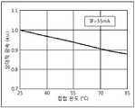
다른 실시예에서, LED 콘트롤러(240)는 LED 채널들 간의 온도 변화에 대한 보상을 추가적으로 제공하는 상이한 버젼의 수식 (1)을 적용한다. 도 6은 접합 온도(junction temperature)의 함수로서, 55mA 순방향 전류와 함께 순방향 바이어스된 LED로부터 방사된 상대적 광속 밀도(relative luminous flux density)의 그래프이다. LED들의 접합 온도가 섭씨 25도부터 85도로 상승됨에 따라, 그래프는 약 12%의 휘도 감소를 예시한다. 이러한 감소는 실질적으로 온도의 선형 함수이다. 따라서, 일 실시예에서, 프로세싱 장치(210)는 다음의 수식을 적용하여 각각의 LED 채널 n에 대하여PWM_outn을 결정한다.In another embodiment, the

단, CT는 실험적으로 결정된 온도의 선형 함수이다. 본 실시예에서, LED 콘트롤러(240)는 LED 스트링들(225)에 대한 온도 데이터를 수신하기 위하여 설치된 추가적인 온도 입력 신호(도시하지 않음)를 포함하도록 수정된다. 온도 데이터는 어떠한 종래의 LED 온도 측정 기법을 이용해서 획득될 수 있다.Where CT is a linear function of the experimentally determined temperature. In this embodiment, the
본 개시를 읽고 나서, 본 발명의 기술 분야의 종사하는 통상의 지식을 가진자는 LED 시스템에 대한 부가적인 다른 디자인들을 여전히 인식할 수 있다. 따라서, 본 발명의 특정 실시예들 및 응용들이 예시되고 서술되어 왔지만, 본 발명은 지금까지 서술된 구성 및 컴포넌트들에 한정되지 않고, 당해 기술 분야의 업자에게 자명한 다양한 수정, 변화, 및 차이가 청구범위에서 정의되는 발명의 기술적 사상 및 권리범위에 벗어남이 없이 본 발명의 방법 및 장치에서의 배열, 동작, 및 상세한 내용들에 만들어 질 수 있다.Having read this disclosure, those of ordinary skill in the art will still recognize additional alternative designs for LED systems. Thus, while specific embodiments and applications of the present invention have been illustrated and described, it is to be understood that the invention is not limited to the precise configuration and components described and that various modifications, changes, Operations, and details in the method and apparatus of the present invention without departing from the spirit and scope of the invention as defined in the claims.
210: 전력 변환 장치 콘트롤러
220: 스위칭 전력 변환 장치
230: LED 드라이버
240: LED 콘트롤러210: power converter controller
220: Switching power converter
230: LED driver
240: LED controller
Claims (22)
Translated fromKorean상기 스위칭 전력 변환 장치의 제1 스위칭 사이클 동안, 상기 제1 스위칭 사이클에 이어지는 상기 스위칭 전력 변환 장치의 제2 스위칭 사이클 동안 상기 하나 이상의 LED 스트링들의 휘도를 제어하기 위한, 업데이트된 휘도 세팅을 수신하는 단계; - 상기 업데이트된 휘도 세팅은 상기 제1 스위칭 사이클 동안의 상기 하나 이상의 LED 스트링들의 상기 휘도를 제어하는 현재 휘도 세팅(present brightness setting)과 다름 -
상기 스위칭 전력 변환 장치의 상기 제2 스위칭 사이클 동안에 상기 하나 이상의 LED 스트링들의 예측 부하를 나타내는 예측 부하 신호를, 상기 스위칭 전력 변환 장치의 상기 제1 스위칭 사이클 동안, 상기 업데이트된 휘도 세팅에 기초하여 생성하는 단계;
상기 제1 스위칭 사이클 동안에 수신된 상기 예측 부하 신호에 기반하여, 상기 제2 스위칭 사이클 동안에 상기 스위칭 전력 변환 장치를 구동하기 위한 듀티 사이클을 결정하는 단계; 및
하나 이상의 LED 스트링들에 전력을 공급하는 출력 전압을 생성하기 위하여 상기 결정된 듀티 사이클을 사용하는 단계
를 포함하는 제어 방법.CLAIMS 1. A method for controlling a switching power converter that supplies power to one or more LED strings,
Receiving an updated luminance setting for controlling the luminance of the one or more LED strings during a second switching cycle of the switching power converter following the first switching cycle during a first switching cycle of the switching power converter ; The updated luminance setting being different from a present brightness setting for controlling the luminance of the one or more LED strings during the first switching cycle,
A predicted load signal indicative of a predicted load of the one or more LED strings during the second switching cycle of the switching power converter is generated based on the updated luminance setting during the first switching cycle of the switching power converter step;
Determining a duty cycle for driving the switching power converter during the second switching cycle based on the predicted load signal received during the first switching cycle; And
Using the determined duty cycle to generate an output voltage that powers one or more LED strings
≪ / RTI >
상기 제2 스위칭 사이클 동안에 상기 스위칭 전력 변환 장치의 출력 전압을 감지하는 단계;
상기 감지된 출력 전압을 바람직한 조절 전압과 비교하는 단계; 및
상기 출력 전압에서 조절을 달성하기 위하여 상기 스위칭 전력 변환 장치의 위칭의 상기 듀티 사이클을 조정하는 단계
를 더 포함하는 제어 방법.The method according to claim 1,
Sensing an output voltage of the switching power converter during the second switching cycle;
Comparing the sensed output voltage to a desired regulated voltage; And
Adjusting the duty cycle of the switching of the switching power converter to achieve regulation in the output voltage
≪ / RTI >
상기 예측 부하 신호는 상기 스위칭 전력 변환 장치의 제2 스위칭 사이클 동안에 상기 하나 이상의 LED 스트링을 통한 예측 누적 평균 전류를 나타내는 제어 방법.The method according to claim 1,
Wherein the predicted load signal represents a predicted cumulative average current through the one or more LED strings during a second switching cycle of the switching power converter.
상기 예측 부하 신호는 상기 LED 스트링들을 통한 프로그램된 전류 및 상기 LED 스트링들을 구동하는 듀티 사이클로부터 결정되는 제어 방법.The method according to claim 1,
Wherein the predicted load signal is determined from a programmed current through the LED strings and a duty cycle driving the LED strings.
상기 예측 부하 신호는 상기 프로그램된 전류 및 상기 각각의 LED 스트링들에 대응하는 상기 듀티 사이클의 곱에 기초하는 제어 방법.5. The method of claim 4,
Wherein the predicted load signal is based on a product of the programmed current and the duty cycle corresponding to each of the LED strings.
상기 스위칭 전력 변환 장치를 구동하기 위한 듀티 사이클을 결정하는 단계는
상기 스위칭 전력 변환 장치에 대하여 감지된 입력 전압, 상기 스위칭 전력 변환 장치의 감지된 출력 전압, 상기 스위칭 전력 변환 장치의 인덕턴스, 상기 스위칭 전력 변환 장치의 스위칭 주기, 및 상기 스위칭 주기 동안에 상기 LED 스트링들을 통한 평균 누적 전류 중에서 적어도 하나에 기초하여 상기 듀티 사이클을 결정하는 단계를 포함하는 제어 방법.The method according to claim 1,
The step of determining a duty cycle for driving the switching power converter
Wherein the switching power conversion device comprises a plurality of LED strings, the input voltage sensed for the switching power converter, the sensed output voltage of the switching power converter, the inductance of the switching power converter, the switching period of the switching power converter, And determining the duty cycle based on at least one of average accumulated current.
상기 하나 이상의 LED 스트링들에 대한 기준치 세팅을 수신하는 단계; 및
상기 각각의 하나 이상의 LED 스트링들을 통한 프로그램된 전류 레벨들을 상기 하나 이상의 LED 스트링들의 전류-전압 특성 및 상기 기준치 전류 세팅에 기초하여 결정하는 단계
를 더 포함하는 제어 방법.The method according to claim 1,
Receiving a reference setting for the one or more LED strings; And
Determining programmed current levels through each of the one or more LED strings based on the current-voltage characteristic of the one or more LED strings and the reference current setting
≪ / RTI >
상기 각각의 하나 이상의 LED 스트링들을 구동하기 위한 듀티 사이클들을 상기 업데이트된 휘도 세팅 및 상기 프로그램된 전류 레벨들에 기초하여 결정하는 단계
를 더 포함하는 제어 방법.8. The method of claim 7,
Determining duty cycles for driving each of the one or more LED strings based on the updated luminance setting and the programmed current levels
≪ / RTI >
상기 듀티 사이클들 및 상기 프로그램된 전류 레벨들을 통신 채널을 통하여 LED 드라이버로 출력하는 단계로서, 상기 LED 드라이버는 상기 듀티 사이클 및 상기 프로그램된 전류 레벨들에 따라서 상기 LED 스트링들을 구동하는 단계
를 더 포함하는 제어 방법.9. The method of claim 8,
Outputting the duty cycles and the programmed current levels to a LED driver via a communication channel, the LED driver driving the LED strings according to the duty cycle and the programmed current levels
≪ / RTI >
비디오 콘트롤러로부터 상기 비디오 콘트롤러의 수직 동기 사이클 당 한 번씩 상기 업데이트된 휘도 세팅을 수신하는 단계; 및
상기 업데이트된 휘도 세팅의 수신에 응답하여, 수직 동기 사이클당 한 번씩 상기 예측 부하 신호를 업데이트하는 단계
를 더 포함하는 제어 방법.The method according to claim 1,
Receiving the updated luminance setting from the video controller once per vertical synchronization cycle of the video controller; And
In response to receiving the updated luminance setting, updating the predicted load signal once per vertical synchronization cycle
≪ / RTI >
상기 예측 부하 신호에 기초하여 제어 신호를 생성하는 단계;
입력 전압을 수신하는 단계; 및
상기 하나 이상의 LED 스트링들에 전력을 공급하는 조절된 출력 전압을 생성하기 위하여 상기 입력 전압을 조절하는 단계로서, 상기 제어 신호는 상기 출력 전압에서 조절을 달성하도록 상기 스위칭 전력 변환 장치의 스위칭을 제어하는 단계
를 더 포함하는 제어 방법.The method according to claim 1,
Generating a control signal based on the predicted load signal;
Receiving an input voltage; And
Adjusting the input voltage to produce a regulated output voltage that powers the one or more LED strings, the control signal controlling switching of the switching power converter to achieve regulation in the output voltage step
≪ / RTI >
스위칭 전력 변환 장치의 제1 스위칭 사이클 동안, 상기 스위칭 전력 변환 장치의 제2 스위칭 사이클 동안 상기 하나 이상의 LED 스트링들의 휘도를 제어하기 위한 업데이트된 휘도 세팅을 수신하고, 상기 스위칭 전력 변환 장치의 상기 제1 스위칭 사이클 동안 상기 하나 이상의 LED 스트링들의 휘도를 제어하는 현재 휘도 세팅과 다른, 상기 업데이트된 휘도 세팅에서 동작하는 상기 하나 이상의 LED 스트링들의 예측 부하를 나타내는 예측 부하 신호를 생성하기 위하여 연결된 LED 콘트롤러; 및 - 상기 제2 스위칭 사이클은 상기 제1 스위칭 사이클에 이어짐 -
상기 스위칭 전력 변환 장치의 상기 제1 스위칭 사이클 동안에 상기 LED 콘트롤러로부터 상기 예측 부하 신호를 수신하고, 상기 제1 스위칭 사이클 동안에 수신된 상기 예측 부하 신호에 기초하여 제어 신호를 생성하고, 상기 제어 신호는 상기 제2 스위칭 사이클 동안 상기 스위칭 전력 변환 장치의 스위칭을 제어하기 위한 듀티 사이클을 가지고, 상기 스위칭 전력 변환 장치는 상기 하나 이상의 LED 스트링들에 전력을 공급하는 전력 변환 콘트롤러
를 포함하는 구동 시스템.
A system for driving one or more LED strings,
During a first switching cycle of the switching power converter, receiving an updated luminance setting for controlling the brightness of the one or more LED strings during a second switching cycle of the switching power converter, An LED controller coupled to generate a predicted load signal indicative of a predicted load of the one or more LED strings operating in the updated luminance setting, the current LED setting being different from a current luminance setting for controlling the brightness of the one or more LED strings during a switching cycle; And the second switching cycle follows the first switching cycle,
Receiving the predicted load signal from the LED controller during the first switching cycle of the switching power converter and generating a control signal based on the predicted load signal received during the first switching cycle, And a duty cycle for controlling switching of the switching power converter during a second switching cycle, the switching power converter comprising: a power conversion controller for powering the one or more LED strings;
≪ / RTI >
상기 전력 변환 콘트롤러는 상기 스위칭 전력 변환 장치의 조절된 출력 전압을 감지하고, 상기 조절된 출력 전압에서 조절을 달성하기 위하여 상기 스위칭 전력 변환 장치의 상기 듀티 사이클을 조정하도록 설치된 구동 시스템.13. The method of claim 12,
Wherein the power conversion controller is configured to sense the regulated output voltage of the switching power converter and to adjust the duty cycle of the switching power converter to achieve regulation at the regulated output voltage.
상기 예측 부하 신호는 상기 스위칭 전력 변환 장치의 제2 스위칭 사이클 동안에 상기 하나 이상의 LED 스트링을 통한 예측 누적 평균 전류를 나타내는 구동 시스템.13. The method of claim 12,
Wherein the predicted load signal represents a predicted cumulative average current through the one or more LED strings during a second switching cycle of the switching power converter.
상기 예측 부하 신호는 프로그램된 전류 및 상기 각각의 LED 스트링들의 각각의 LED에 대응하는 상기 듀티 사이클의 곱에 기초하는 구동 시스템.15. The method of claim 14,
Wherein the predicted load signal is based on a product of a programmed current and the duty cycle corresponding to each LED of each of the LED strings.
상기 예측 부하 신호는 상기 LED 스트링들을 통한 프로그램된 전류 및 상기 LED 스트링들을 구동하는 듀티 사이클들로부터 결정되는 구동 시스템.13. The method of claim 12,
Wherein the predicted load signal is determined from the programmed current through the LED strings and the duty cycles driving the LED strings.
상기 전력 변환 콘트롤러는 상기 스위칭 전력 변환 장치에 대하여 감지된 입력 전압, 상기 스위칭 전력 변환 장치의 감지된 출력 전압, 상기 스위칭 전력 변환 장치의 인덕턴스, 상기 스위칭 전력 변환 장치의 스위칭 주기, 및 상기 스위칭 주기 동안에 상기 LED 스트링들을 통한 평균 누적 전류에 기초하여 상기 스위칭 전력 변환 장치를 구동하는 상기 듀티 사이클을 결정하는 구동 시스템.13. The method of claim 12,
Wherein the power conversion controller is operable to convert the input voltage sensed for the switching power converter, the sensed output voltage of the switching power converter, the inductance of the switching power converter, the switching period of the switching power converter, And determines the duty cycle to drive the switching power converter based on an average accumulated current through the LED strings.
상기 LED 콘트롤러는 상기 각각의 하나 이상의 LED 스트링들을 통한 프로그램된 전류 레벨들을 상기 하나 이상의 LED 스트링들의 전류-전압 특성에 기초하여 결정하도록 설치된 구동 시스템.13. The method of claim 12,
Wherein the LED controller is configured to determine programmed current levels through each of the one or more LED strings based on a current-voltage characteristic of the one or more LED strings.
상기 LED 콘트롤러는 상기 각각의 하나 이상의 LED 스트링들을 구동하기 위한 듀티 사이클들을 상기 업데이트된 휘도 세팅 및 상기 프로그램된 전류 레벨들에 기초하여 결정하도록 설치된 구동 시스템.19. The method of claim 18,
Wherein the LED controller is configured to determine duty cycles for driving each of the one or more LED strings based on the updated luminance setting and the programmed current levels.
상기 LED 콘트롤러 및 LED 드라이버 사이에서 통신하기 위한 통신 채널을 더 포함하고,
상기 LED 콘트롤러는 상기 결정된 듀티 사이클들 및 상기 프로그램된 전류 레벨들을 상기 통신 채널을 통하여 상기 LED 드라이버로 출력하는 구동 시스템.20. The method of claim 19,
Further comprising a communication channel for communicating between the LED controller and the LED driver,
And the LED controller outputs the determined duty cycles and the programmed current levels to the LED driver via the communication channel.
상기 LED 콘트롤러는 비디오 콘트롤러로부터 상기 비디오 콘트롤러의 수직 동기 사이클당 한 번씩 상기 업데이트된 휘도 세팅을 수신하고, 상기 업데이트된 휘도 세팅의 수신에 응답하여, 수직 동기 사이클당 한 번씩 상기 예측 부하 신호를 업데이트하는 구동 시스템.13. The method of claim 12,
The LED controller receives the updated luminance setting from the video controller once per vertical sync cycle of the video controller and updates the predicted load signal once per vertical sync cycle in response to receiving the updated luminance setting Drive system.
상기 LED 콘트롤러로부터 상기 제어 신호를 수신하고, 상기 하나 이상의 LED 스트링들에 전력을 공급하는 조절 출력 전압을 생성하기 위하여 입력 전압을 조절하는 상기 스위칭 전력 변환 장치
를 더 포함하고,
상기 제어 신호는 상기 출력 전압에서 조절을 달성하도록 상기 스위칭 전력 변환 장치의 스위칭을 제어하는 구동 시스템.13. The method of claim 12,
For receiving the control signal from the LED controller and for regulating an input voltage to generate an adjusted output voltage to power the one or more LED strings,
Further comprising:
Wherein the control signal controls switching of the switching power converter to achieve regulation in the output voltage.
Applications Claiming Priority (2)
| Application Number | Priority Date | Filing Date | Title |
|---|---|---|---|
| US13/339,196 | 2011-12-28 | ||
| US13/339,196US8791647B2 (en) | 2011-12-28 | 2011-12-28 | Predictive control of power converter for LED driver |
Publications (2)
| Publication Number | Publication Date |
|---|---|
| KR20130076710A KR20130076710A (en) | 2013-07-08 |
| KR101508418B1true KR101508418B1 (en) | 2015-04-07 |
Family
ID=48679732
Family Applications (1)
| Application Number | Title | Priority Date | Filing Date |
|---|---|---|---|
| KR20120143254AActiveKR101508418B1 (en) | 2011-12-28 | 2012-12-11 | Predictive control of power converter for led driver |
Country Status (3)
| Country | Link |
|---|---|
| US (1) | US8791647B2 (en) |
| KR (1) | KR101508418B1 (en) |
| CN (1) | CN103188853B (en) |
Cited By (1)
| Publication number | Priority date | Publication date | Assignee | Title |
|---|---|---|---|---|
| US10249229B2 (en) | 2015-05-14 | 2019-04-02 | Silicon Works Co., Ltd. | Power switching circuit and method for controlling same |
Families Citing this family (69)
| Publication number | Priority date | Publication date | Assignee | Title |
|---|---|---|---|---|
| US10210750B2 (en) | 2011-09-13 | 2019-02-19 | Lutron Electronics Co., Inc. | System and method of extending the communication range in a visible light communication system |
| US8773336B2 (en) | 2008-09-05 | 2014-07-08 | Ketra, Inc. | Illumination devices and related systems and methods |
| US9276766B2 (en) | 2008-09-05 | 2016-03-01 | Ketra, Inc. | Display calibration systems and related methods |
| US9509525B2 (en) | 2008-09-05 | 2016-11-29 | Ketra, Inc. | Intelligent illumination device |
| USRE50468E1 (en) | 2008-09-05 | 2025-06-24 | Lutron Technology Company Llc | Intelligent illumination device |
| USRE49454E1 (en) | 2010-09-30 | 2023-03-07 | Lutron Technology Company Llc | Lighting control system |
| US9386668B2 (en) | 2010-09-30 | 2016-07-05 | Ketra, Inc. | Lighting control system |
| US8564270B2 (en) | 2012-03-15 | 2013-10-22 | Iwatt Inc. | On-time compensation for switching power converters |
| KR20130130526A (en)* | 2012-05-22 | 2013-12-02 | 삼성디스플레이 주식회사 | Method of driving a light source, light source apparatus performing the method and display apparatus having the light source apparatus |
| JP2014132320A (en)* | 2013-01-07 | 2014-07-17 | Panasonic Liquid Crystal Display Co Ltd | Liquid crystal display device |
| US9866117B2 (en)* | 2013-03-11 | 2018-01-09 | Cree, Inc. | Power supply with adaptive-controlled output voltage |
| US9425687B2 (en) | 2013-03-11 | 2016-08-23 | Cree, Inc. | Methods of operating switched mode power supply circuits using adaptive filtering and related controller circuits |
| CN104344374B (en)* | 2013-07-26 | 2018-05-15 | 展晶科技(深圳)有限公司 | Light emitting diode illuminating apparatus |
| US9237620B1 (en) | 2013-08-20 | 2016-01-12 | Ketra, Inc. | Illumination device and temperature compensation method |
| US9332598B1 (en) | 2013-08-20 | 2016-05-03 | Ketra, Inc. | Interference-resistant compensation for illumination devices having multiple emitter modules |
| US9155155B1 (en) | 2013-08-20 | 2015-10-06 | Ketra, Inc. | Overlapping measurement sequences for interference-resistant compensation in light emitting diode devices |
| USRE48956E1 (en) | 2013-08-20 | 2022-03-01 | Lutron Technology Company Llc | Interference-resistant compensation for illumination devices using multiple series of measurement intervals |
| US9578724B1 (en) | 2013-08-20 | 2017-02-21 | Ketra, Inc. | Illumination device and method for avoiding flicker |
| USRE48955E1 (en) | 2013-08-20 | 2022-03-01 | Lutron Technology Company Llc | Interference-resistant compensation for illumination devices having multiple emitter modules |
| US9247605B1 (en) | 2013-08-20 | 2016-01-26 | Ketra, Inc. | Interference-resistant compensation for illumination devices |
| US9360174B2 (en) | 2013-12-05 | 2016-06-07 | Ketra, Inc. | Linear LED illumination device with improved color mixing |
| US9651632B1 (en) | 2013-08-20 | 2017-05-16 | Ketra, Inc. | Illumination device and temperature calibration method |
| US9345097B1 (en) | 2013-08-20 | 2016-05-17 | Ketra, Inc. | Interference-resistant compensation for illumination devices using multiple series of measurement intervals |
| US9769899B2 (en) | 2014-06-25 | 2017-09-19 | Ketra, Inc. | Illumination device and age compensation method |
| US9736895B1 (en) | 2013-10-03 | 2017-08-15 | Ketra, Inc. | Color mixing optics for LED illumination device |
| US9374855B2 (en)* | 2013-10-24 | 2016-06-21 | Osram Sylvania Inc. | Power line communication for lighting systems |
| US20150220128A1 (en)* | 2014-02-04 | 2015-08-06 | Infineon Technologies Ag | Method and Apparatus for Use in a Data Processing System |
| JP6303745B2 (en)* | 2014-04-11 | 2018-04-04 | ミツミ電機株式会社 | LED lighting power supply device, LED lighting device and dimming current adjusting method |
| US9557214B2 (en) | 2014-06-25 | 2017-01-31 | Ketra, Inc. | Illumination device and method for calibrating an illumination device over changes in temperature, drive current, and time |
| US10161786B2 (en) | 2014-06-25 | 2018-12-25 | Lutron Ketra, Llc | Emitter module for an LED illumination device |
| US9392663B2 (en) | 2014-06-25 | 2016-07-12 | Ketra, Inc. | Illumination device and method for controlling an illumination device over changes in drive current and temperature |
| US9736903B2 (en) | 2014-06-25 | 2017-08-15 | Ketra, Inc. | Illumination device and method for calibrating and controlling an illumination device comprising a phosphor converted LED |
| CN107078635B (en) | 2014-06-27 | 2019-07-23 | 飞利浦灯具控股公司 | Power supply system and method and circuit using the same |
| EP3000166A4 (en)* | 2014-08-19 | 2016-10-05 | Abbeydorney Holdings Ltd | Driving circuit, lighting device and method of reducing power dissipation |
| US9392660B2 (en) | 2014-08-28 | 2016-07-12 | Ketra, Inc. | LED illumination device and calibration method for accurately characterizing the emission LEDs and photodetector(s) included within the LED illumination device |
| US9510416B2 (en) | 2014-08-28 | 2016-11-29 | Ketra, Inc. | LED illumination device and method for accurately controlling the intensity and color point of the illumination device over time |
| KR101566515B1 (en)* | 2014-11-28 | 2015-11-05 | 류태하 | Flicker-Free AC LED Illumination System |
| US9485813B1 (en) | 2015-01-26 | 2016-11-01 | Ketra, Inc. | Illumination device and method for avoiding an over-power or over-current condition in a power converter |
| US9237623B1 (en) | 2015-01-26 | 2016-01-12 | Ketra, Inc. | Illumination device and method for determining a maximum lumens that can be safely produced by the illumination device to achieve a target chromaticity |
| US9237612B1 (en) | 2015-01-26 | 2016-01-12 | Ketra, Inc. | Illumination device and method for determining a target lumens that can be safely produced by an illumination device at a present temperature |
| JP6528195B2 (en)* | 2015-03-04 | 2019-06-12 | パナソニックIpマネジメント株式会社 | Lighting device and correction method of lighting device |
| US10278242B2 (en)* | 2015-04-09 | 2019-04-30 | Diddes Incorporated | Thermal and power optimization for linear regulator |
| JP6560070B2 (en)* | 2015-09-10 | 2019-08-14 | Necプラットフォームズ株式会社 | Power supply device, power supply control method thereof, and computer program |
| EP3322077A1 (en)* | 2016-11-15 | 2018-05-16 | Nxp B.V. | Dc-dc converter controller |
| CN106875899B (en)* | 2017-03-20 | 2019-07-26 | 联想(北京)有限公司 | A kind of control method and electronic equipment showing output device |
| CN107027221B (en)* | 2017-05-09 | 2024-03-15 | 赛尔富电子有限公司 | Plant LED lamp illumination control system |
| US10237936B2 (en)* | 2017-08-16 | 2019-03-19 | Apple Inc. | Split driver backlight systems and methods |
| JP7218353B2 (en)* | 2017-08-18 | 2023-02-06 | シグニファイ ホールディング ビー ヴィ | Monitor device for lighting arrangement, driver using monitor arrangement and driving method |
| US11272599B1 (en) | 2018-06-22 | 2022-03-08 | Lutron Technology Company Llc | Calibration procedure for a light-emitting diode light source |
| US12198605B2 (en) | 2019-03-29 | 2025-01-14 | Creeled, Inc. | Active control of light emitting diodes and light emitting diode displays |
| US11727857B2 (en) | 2019-03-29 | 2023-08-15 | Creeled, Inc. | Active control of light emitting diodes and light emitting diode displays |
| US12142716B2 (en) | 2019-03-29 | 2024-11-12 | Creeled, Inc. | Active control of light emitting diodes and light emitting diode displays |
| US10531527B1 (en)* | 2019-04-26 | 2020-01-07 | Infineon Technologies Ag | Circuit for controlling delivery of an electrical signal to one or more light-emitting diode strings |
| US10560990B1 (en)* | 2019-04-26 | 2020-02-11 | Infineon Technologies Ag | Light emitting diode circuit with accurate current monitoring of two or more different LED strings |
| TWI759619B (en)* | 2019-08-06 | 2022-04-01 | 隆達電子股份有限公司 | Pixel circuit and driving method |
| EP3908084A1 (en)* | 2020-05-06 | 2021-11-10 | Tridonic GmbH & Co. KG | A switched converter |
| US11358518B2 (en) | 2020-10-06 | 2022-06-14 | Infineon Technologies Ag | Light function control redundancy when changing the light intensity of pixelated vehicle headlamps |
| CN113450704B (en)* | 2020-10-13 | 2022-04-19 | 重庆康佳光电技术研究院有限公司 | LED driving method, driving unit, display device and readable storage medium |
| CN114513128A (en)* | 2020-11-17 | 2022-05-17 | 意法设计与应用股份有限公司 | Current supply system and method of operation, associated integrated circuit and power supply system |
| EP4002958B1 (en)* | 2020-11-17 | 2024-07-17 | STMicroelectronics S.r.l. | A current supply system and a method of operating said current supply system |
| US11087672B1 (en)* | 2020-12-09 | 2021-08-10 | Huayuan Semiconductor (Shenzhen) Limited Company | Display device with selectable LED current levels based on brightness data |
| CN112636598B (en)* | 2021-03-11 | 2021-05-25 | 深圳市正浩创新科技有限公司 | Control method, device and system of synchronous BUCK circuit and electronic device |
| EP4085449A1 (en) | 2021-03-23 | 2022-11-09 | Google LLC | Baseline and shaped pulse driving for micro-light emitting diode display |
| CN113347759B (en)* | 2021-05-26 | 2023-03-28 | 深圳市必易微电子股份有限公司 | Five-channel LED driving circuit, driving method and LED lamp |
| US11864280B2 (en)* | 2021-10-18 | 2024-01-02 | Aes Global Holdings Pte Ltd. | Light driver calibration |
| EP4476714A1 (en) | 2022-02-07 | 2024-12-18 | Creeled, Inc. | Light-emitting diodes with mixed clock domain signaling |
| US12014673B2 (en) | 2022-02-07 | 2024-06-18 | Creeled, Inc. | Light-emitting diodes with mixed clock domain signaling |
| US12014677B1 (en) | 2023-04-10 | 2024-06-18 | Creeled, Inc. | Light-emitting diode packages with transformation and shifting of pulse width modulation signals and related methods |
| US12437707B2 (en) | 2023-09-27 | 2025-10-07 | Creeled, Inc. | Pseudo-exponential encoding for light-emitting devices and related methods |
Citations (2)
| Publication number | Priority date | Publication date | Assignee | Title |
|---|---|---|---|---|
| KR20100075046A (en)* | 2008-12-24 | 2010-07-02 | 엘지디스플레이 주식회사 | Driving apparatus for liquid crystal display device and method for driving the same |
| US20110187276A1 (en)* | 2006-11-21 | 2011-08-04 | Exclara Inc. | Time Division Modulation With Average Current Regulation for Independent Control of Arrays of Light Emitting Diodes |
Family Cites Families (9)
| Publication number | Priority date | Publication date | Assignee | Title |
|---|---|---|---|---|
| CN100530920C (en)* | 2004-04-19 | 2009-08-19 | 英特赛尔美国股份有限公司 | Linear predictive system and method for DC-DC converter |
| US8018171B1 (en)* | 2007-03-12 | 2011-09-13 | Cirrus Logic, Inc. | Multi-function duty cycle modifier |
| US7880400B2 (en)* | 2007-09-21 | 2011-02-01 | Exclara, Inc. | Digital driver apparatus, method and system for solid state lighting |
| US7928670B2 (en) | 2008-06-30 | 2011-04-19 | Iwatt Inc. | LED driver with multiple feedback loops |
| US8049439B2 (en)* | 2009-01-30 | 2011-11-01 | Freescale Semiconductor, Inc. | LED driver with dynamic headroom control |
| US8305007B2 (en)* | 2009-07-17 | 2012-11-06 | Freescale Semiconductor, Inc. | Analog-to-digital converter with non-uniform accuracy |
| US8334662B2 (en) | 2009-09-11 | 2012-12-18 | Iwatt Inc. | Adaptive switch mode LED driver |
| US8587956B2 (en)* | 2010-02-05 | 2013-11-19 | Luxera, Inc. | Integrated electronic device for controlling light emitting diodes |
| CN101917118A (en)* | 2010-08-23 | 2010-12-15 | 东南大学 | Digital Predictive Control System and Method for Switching DC-DC Converter |
- 2011
- 2011-12-28USUS13/339,196patent/US8791647B2/enactiveActive
- 2012
- 2012-11-29CNCN201210521671.3Apatent/CN103188853B/enactiveActive
- 2012-12-11KRKR20120143254Apatent/KR101508418B1/enactiveActive
Patent Citations (2)
| Publication number | Priority date | Publication date | Assignee | Title |
|---|---|---|---|---|
| US20110187276A1 (en)* | 2006-11-21 | 2011-08-04 | Exclara Inc. | Time Division Modulation With Average Current Regulation for Independent Control of Arrays of Light Emitting Diodes |
| KR20100075046A (en)* | 2008-12-24 | 2010-07-02 | 엘지디스플레이 주식회사 | Driving apparatus for liquid crystal display device and method for driving the same |
Cited By (1)
| Publication number | Priority date | Publication date | Assignee | Title |
|---|---|---|---|---|
| US10249229B2 (en) | 2015-05-14 | 2019-04-02 | Silicon Works Co., Ltd. | Power switching circuit and method for controlling same |
Also Published As
| Publication number | Publication date |
|---|---|
| CN103188853B (en) | 2015-04-15 |
| KR20130076710A (en) | 2013-07-08 |
| US20130169172A1 (en) | 2013-07-04 |
| CN103188853A (en) | 2013-07-03 |
| US8791647B2 (en) | 2014-07-29 |
Similar Documents
| Publication | Publication Date | Title |
|---|---|---|
| KR101508418B1 (en) | Predictive control of power converter for led driver | |
| US8710752B2 (en) | Adaptive switch mode LED system | |
| US10396659B2 (en) | Load driving device, and lighting apparatus and liquid crystal display device using the same | |
| US9451664B2 (en) | Adaptive switch mode LED driver | |
| US8253352B2 (en) | Circuits and methods for powering light sources | |
| US10278242B2 (en) | Thermal and power optimization for linear regulator | |
| US7843150B2 (en) | Power regulation for LED strings | |
| US10136487B2 (en) | Power optimization for linear regulator | |
| US8957607B2 (en) | DC-DC converter using hysteretic control and associated methods | |
| US20190334437A1 (en) | Load driving device, and lighting apparatus and liquid crystal display device using the same | |
| CN203086782U (en) | LED illuminating controller, driver, illuminating device, and display device | |
| KR20150014592A (en) | Multi channel light emitting diode driver | |
| KR101854693B1 (en) | Backlight unit | |
| CN103857140A (en) | LED light-emitting controller, driver, drive method, illuminating equipment and display equipment | |
| Kang et al. | A new low voltage detecting method for multi-string LED BLU circuit |
Legal Events
| Date | Code | Title | Description |
|---|---|---|---|
| A201 | Request for examination | ||
| PA0109 | Patent application | St.27 status event code:A-0-1-A10-A12-nap-PA0109 | |
| PA0201 | Request for examination | St.27 status event code:A-1-2-D10-D11-exm-PA0201 | |
| PG1501 | Laying open of application | St.27 status event code:A-1-1-Q10-Q12-nap-PG1501 | |
| PN2301 | Change of applicant | St.27 status event code:A-3-3-R10-R13-asn-PN2301 St.27 status event code:A-3-3-R10-R11-asn-PN2301 | |
| E902 | Notification of reason for refusal | ||
| PE0902 | Notice of grounds for rejection | St.27 status event code:A-1-2-D10-D21-exm-PE0902 | |
| P11-X000 | Amendment of application requested | St.27 status event code:A-2-2-P10-P11-nap-X000 | |
| P13-X000 | Application amended | St.27 status event code:A-2-2-P10-P13-nap-X000 | |
| E701 | Decision to grant or registration of patent right | ||
| PE0701 | Decision of registration | St.27 status event code:A-1-2-D10-D22-exm-PE0701 | |
| PR0701 | Registration of establishment | St.27 status event code:A-2-4-F10-F11-exm-PR0701 | |
| PR1002 | Payment of registration fee | St.27 status event code:A-2-2-U10-U11-oth-PR1002 Fee payment year number:1 | |
| PG1601 | Publication of registration | St.27 status event code:A-4-4-Q10-Q13-nap-PG1601 | |
| FPAY | Annual fee payment | Payment date:20180320 Year of fee payment:4 | |
| PR1001 | Payment of annual fee | St.27 status event code:A-4-4-U10-U11-oth-PR1001 Fee payment year number:4 | |
| FPAY | Annual fee payment | Payment date:20190318 Year of fee payment:5 | |
| PR1001 | Payment of annual fee | St.27 status event code:A-4-4-U10-U11-oth-PR1001 Fee payment year number:5 | |
| P22-X000 | Classification modified | St.27 status event code:A-4-4-P10-P22-nap-X000 | |
| P22-X000 | Classification modified | St.27 status event code:A-4-4-P10-P22-nap-X000 | |
| PR1001 | Payment of annual fee | St.27 status event code:A-4-4-U10-U11-oth-PR1001 Fee payment year number:6 | |
| P22-X000 | Classification modified | St.27 status event code:A-4-4-P10-P22-nap-X000 | |
| PR1001 | Payment of annual fee | St.27 status event code:A-4-4-U10-U11-oth-PR1001 Fee payment year number:7 | |
| PR1001 | Payment of annual fee | St.27 status event code:A-4-4-U10-U11-oth-PR1001 Fee payment year number:8 | |
| PR1001 | Payment of annual fee | St.27 status event code:A-4-4-U10-U11-oth-PR1001 Fee payment year number:9 | |
| PR1001 | Payment of annual fee | St.27 status event code:A-4-4-U10-U11-oth-PR1001 Fee payment year number:10 | |
| PR1001 | Payment of annual fee | St.27 status event code:A-4-4-U10-U11-oth-PR1001 Fee payment year number:11 | |
| P22-X000 | Classification modified | St.27 status event code:A-4-4-P10-P22-nap-X000 |