KR101506098B1 - Oxide semiconductor transistor without threshold voltage change in nbis method for manufacturing the same - Google Patents
Oxide semiconductor transistor without threshold voltage change in nbis method for manufacturing the sameDownload PDFInfo
- Publication number
- KR101506098B1 KR101506098B1KR1020130153421AKR20130153421AKR101506098B1KR 101506098 B1KR101506098 B1KR 101506098B1KR 1020130153421 AKR1020130153421 AKR 1020130153421AKR 20130153421 AKR20130153421 AKR 20130153421AKR 101506098 B1KR101506098 B1KR 101506098B1
- Authority
- KR
- South Korea
- Prior art keywords
- electrode
- gate electrode
- oxide semiconductor
- gate
- oxide
- Prior art date
- Legal status (The legal status is an assumption and is not a legal conclusion. Google has not performed a legal analysis and makes no representation as to the accuracy of the status listed.)
- Active
Links
- 239000004065semiconductorSubstances0.000titleclaimsabstractdescription76
- 238000004519manufacturing processMethods0.000titleclaimsabstractdescription10
- 238000000034methodMethods0.000titleclaimsdescription9
- 239000000758substrateSubstances0.000claimsabstractdescription15
- 239000010410layerSubstances0.000claimsdescription27
- XLOMVQKBTHCTTD-UHFFFAOYSA-NZinc monoxideChemical compound[Zn]=OXLOMVQKBTHCTTD-UHFFFAOYSA-N0.000claimsdescription13
- 239000011241protective layerSubstances0.000claimsdescription11
- 239000000463materialSubstances0.000claimsdescription7
- -1aluminum zinc tin oxideChemical compound0.000claimsdescription6
- 229910052738indiumInorganic materials0.000claimsdescription5
- APFVFJFRJDLVQX-UHFFFAOYSA-Nindium atomChemical compound[In]APFVFJFRJDLVQX-UHFFFAOYSA-N0.000claimsdescription5
- 229910044991metal oxideInorganic materials0.000claimsdescription5
- 150000004706metal oxidesChemical class0.000claimsdescription5
- 239000011787zinc oxideSubstances0.000claimsdescription5
- GYHNNYVSQQEPJS-UHFFFAOYSA-NGalliumChemical compound[Ga]GYHNNYVSQQEPJS-UHFFFAOYSA-N0.000claimsdescription4
- 229910052733galliumInorganic materials0.000claimsdescription4
- AMGQUBHHOARCQH-UHFFFAOYSA-Nindium;oxotinChemical compound[In].[Sn]=OAMGQUBHHOARCQH-UHFFFAOYSA-N0.000claimsdescription3
- HRHKULZDDYWVBE-UHFFFAOYSA-Nindium;oxozinc;tinChemical compound[In].[Sn].[Zn]=OHRHKULZDDYWVBE-UHFFFAOYSA-N0.000claimsdescription3
- KYKLWYKWCAYAJY-UHFFFAOYSA-Noxotin;zincChemical compound[Zn].[Sn]=OKYKLWYKWCAYAJY-UHFFFAOYSA-N0.000claimsdescription3
- YVTHLONGBIQYBO-UHFFFAOYSA-Nzinc indium(3+) oxygen(2-)Chemical compound[O--].[Zn++].[In+3]YVTHLONGBIQYBO-UHFFFAOYSA-N0.000claimsdescription3
- FTWITUGAJAOTCJ-UHFFFAOYSA-N[Zn].[In].[Hf]Chemical compound[Zn].[In].[Hf]FTWITUGAJAOTCJ-UHFFFAOYSA-N0.000claimsdescription2
- AJNVQOSZGJRYEI-UHFFFAOYSA-Ndigallium;oxygen(2-)Chemical compound[O-2].[O-2].[O-2].[Ga+3].[Ga+3]AJNVQOSZGJRYEI-UHFFFAOYSA-N0.000claimsdescription2
- 229910001195gallium oxideInorganic materials0.000claimsdescription2
- 238000010586diagramMethods0.000description9
- 239000010408filmSubstances0.000description8
- VYPSYNLAJGMNEJ-UHFFFAOYSA-Nsilicon dioxideInorganic materialsO=[Si]=OVYPSYNLAJGMNEJ-UHFFFAOYSA-N0.000description7
- 239000010409thin filmSubstances0.000description7
- 229910052814silicon oxideInorganic materials0.000description6
- 238000005286illuminationMethods0.000description4
- 238000012546transferMethods0.000description4
- 229920001621AMOLEDPolymers0.000description3
- ZOKXTWBITQBERF-UHFFFAOYSA-NMolybdenumChemical compound[Mo]ZOKXTWBITQBERF-UHFFFAOYSA-N0.000description3
- 239000007769metal materialSubstances0.000description3
- 238000012986modificationMethods0.000description3
- 230000004048modificationEffects0.000description3
- 229910052750molybdenumInorganic materials0.000description3
- 239000011733molybdenumSubstances0.000description3
- 230000003071parasitic effectEffects0.000description3
- 238000012360testing methodMethods0.000description3
- 239000012212insulatorSubstances0.000description2
- 229910052751metalInorganic materials0.000description2
- 239000002184metalSubstances0.000description2
- 229920002120photoresistant polymerPolymers0.000description2
- 230000000903blocking effectEffects0.000description1
- 238000000151depositionMethods0.000description1
- 238000011161developmentMethods0.000description1
- 230000009977dual effectEffects0.000description1
- 238000005530etchingMethods0.000description1
- 239000011521glassSubstances0.000description1
- 238000005259measurementMethods0.000description1
- 238000002161passivationMethods0.000description1
- 239000004033plasticSubstances0.000description1
- 230000002250progressing effectEffects0.000description1
- 239000010453quartzSubstances0.000description1
- 238000011160researchMethods0.000description1
- 230000007704transitionEffects0.000description1
- YSRUGFMGLKANGO-UHFFFAOYSA-Nzinc hafnium(4+) indium(3+) oxygen(2-)Chemical compound[O-2].[Zn+2].[In+3].[Hf+4]YSRUGFMGLKANGO-UHFFFAOYSA-N0.000description1
Images


Classifications
- H—ELECTRICITY
- H10—SEMICONDUCTOR DEVICES; ELECTRIC SOLID-STATE DEVICES NOT OTHERWISE PROVIDED FOR
- H10D—INORGANIC ELECTRIC SEMICONDUCTOR DEVICES
- H10D30/00—Field-effect transistors [FET]
- H10D30/60—Insulated-gate field-effect transistors [IGFET]
- H10D30/67—Thin-film transistors [TFT]
- H10D30/6729—Thin-film transistors [TFT] characterised by the electrodes
- H10D30/673—Thin-film transistors [TFT] characterised by the electrodes characterised by the shapes, relative sizes or dispositions of the gate electrodes
- H10D30/6733—Multi-gate TFTs
- H10D30/6734—Multi-gate TFTs having gate electrodes arranged on both top and bottom sides of the channel, e.g. dual-gate TFTs
- H—ELECTRICITY
- H10—SEMICONDUCTOR DEVICES; ELECTRIC SOLID-STATE DEVICES NOT OTHERWISE PROVIDED FOR
- H10D—INORGANIC ELECTRIC SEMICONDUCTOR DEVICES
- H10D30/00—Field-effect transistors [FET]
- H10D30/60—Insulated-gate field-effect transistors [IGFET]
- H10D30/67—Thin-film transistors [TFT]
- H10D30/6729—Thin-film transistors [TFT] characterised by the electrodes
- H10D30/673—Thin-film transistors [TFT] characterised by the electrodes characterised by the shapes, relative sizes or dispositions of the gate electrodes
- H—ELECTRICITY
- H10—SEMICONDUCTOR DEVICES; ELECTRIC SOLID-STATE DEVICES NOT OTHERWISE PROVIDED FOR
- H10D—INORGANIC ELECTRIC SEMICONDUCTOR DEVICES
- H10D30/00—Field-effect transistors [FET]
- H10D30/60—Insulated-gate field-effect transistors [IGFET]
- H10D30/67—Thin-film transistors [TFT]
- H10D30/674—Thin-film transistors [TFT] characterised by the active materials
- H10D30/6755—Oxide semiconductors, e.g. zinc oxide, copper aluminium oxide or cadmium stannate
Landscapes
- Thin Film Transistor (AREA)
Abstract
Description
Translated fromKorean본 발명의 실시예들은 NBIS(Negative Bias Illumination Stress)에 대한 신뢰성을 향상시키며 고성능의 전기적 특성을 가지는 디스플레이 장치의 화소 소자로 사용되는 산화물 반도체 트랜지스터 및 이의 제조 방법에 관한 것이다.Embodiments of the present invention relate to an oxide semiconductor transistor used as a pixel element of a display device which improves the reliability of NBIS (Negative Bias Illumination Stress) and has high-performance electrical characteristics, and a method of manufacturing the same.
최근 산화물 반도체인 a-IGZO(Indium Gallium Zinc Oxide)를 이용한 구동소자로 구동되는 디스플레이 장치의 개발이 빠르게 진행되고 있다. 이와 더불어, 디스플레이 소자의 구동에 기본적으로 필요한 인버터뿐만 아니라 이를 이용한 구동회로에 대해서도 상당 부분 연구가 진행되고 있다.Recently, the development of a display device driven by a driving device using an a-IGZO (Indium Gallium Zinc Oxide) oxide semiconductor is rapidly progressing. In addition, considerable research is being conducted on not only an inverter necessary for driving a display device but also a driving circuit using the same.
이와 관련하여, 한국특허출원 제10-2012-0087910호에서는 E/S(Etch/Stopper) 타입의 듀얼 게이트 구조의 산화물 반도체 박막 트랜지스터를 개시하고 있다.In this connection, Korean Patent Application No. 10-2012-0087910 discloses an oxide semiconductor thin film transistor of an E / S (Etch / Stopper) type dual gate structure.
그러나, 상기한 종래의 산화물 반도체 박막 트랜지스터는 하부 게이트 전극과 상부 게이트 전극이 전기적으로 분리되어 있고, 상부 게이트 전극으로는 전압이 인가되지 않는 특성을 가진다.However, in the conventional oxide semiconductor thin film transistor, the lower gate electrode and the upper gate electrode are electrically separated from each other, and the upper gate electrode has no voltage applied thereto.
한편, 상기한 산화물 반도체 박막 트랜지스터에 있어, 상부 게이트 전극에 특정 전압을 인가하는 경우, 해당 트랜지스터를 디플레이션 모드(Depletion Mode)로 사용할 수 있지만, 상부 게이트 전극에 인가되는 전압과 하부 게이트 전극에 인가되는 전압의 차이가 발생하는 경우, 전기적 특성이 열화되는 단점이 있었다.In the oxide semiconductor thin film transistor described above, when a specific voltage is applied to the upper gate electrode, the transistor may be used in a deflation mode, but a voltage applied to the upper gate electrode and a voltage applied to the lower gate electrode When a difference in voltage occurs, there is a disadvantage that electrical characteristics are deteriorated.
그리고, 상부 게이트 전극과 소스 전극/드레인 전극 사이에는 기생 전압이 발생하게 되는데, 이는 고성능의 전기적 특성을 가지는 산화물 반도체 박막 트랜지스터의 특성이 열화되는 단점이 있었다.A parasitic voltage is generated between the upper gate electrode and the source electrode / drain electrode, which deteriorates characteristics of the oxide semiconductor thin film transistor having high-performance electrical characteristics.
또한, 산화물 반도체 박막 트랜지스터의 신뢰성 테스트 중 하나인 NBIS(Negative Bias Illumination Stress)에 대해, a-IGZO 박막 트랜지스터는 전기적 특성이 심하게 변하는 단점이 있었다.In addition, with respect to NBIS (Negative Bias Illumination Stress), which is one of the reliability tests of oxide semiconductor thin film transistors, the a-IGZO thin film transistor has a disadvantage that electric characteristics are severely changed.
상기한 바와 같은 종래기술의 문제점을 해결하기 위해, 본 발명에서는 NBIS(Negative Bias Illumination Stress)에 대한 신뢰성을 향상시키며 고성능의 전기적 특성을 가지는 디스플레이 장치의 화소 소자로 사용되는 산화물 반도체 트랜지스터 및 이의 제조 방법을 제안하고자 한다.In order to solve the problems of the prior art as described above, the present invention provides an oxide semiconductor transistor used as a pixel element of a display device which improves reliability against NBIS (Negative Bias Illumination Stress) and has high-performance electrical characteristics, and a method of manufacturing the same .
본 발명의 다른 목적들은 하기의 실시예를 통해 당업자에 의해 도출될 수 있을 것이다.Other objects of the invention will be apparent to those skilled in the art from the following examples.
상기한 목적을 달성하기 위해 본 발명의 바람직한 일 실시예에 따르면, 디스플레이 장치의 화소 소자로 사용되는 산화물 반도체 트랜지스터에 있어서, 기판; 상기 기판 위에 위치하는 제1 게이트 전극; 상기 제1 게이트 전극 위에 위치하는 소스 전극 및 드레인 전극; 및 상기 소스 전극 및 상기 드레인 전극 위에 위치하는 제2 게이트 전극;을 포함하되, 상기 제2 게이트 전극의 일단과 상기 소스 전극 사이의 수직한 거리의 폭 및 상기 제2 게이트 전극의 타단과 상기 드레인 전극 사이의 수직한 거리의 폭 중 적어도 하나는 0.5μm 이상 5μm 이하의 값을 가지는 산화물 반도체 트랜지스터가 제공된다.In order to achieve the above object, according to a preferred embodiment of the present invention, an oxide semiconductor transistor used as a pixel element of a display device comprises: a substrate; A first gate electrode located on the substrate; A source electrode and a drain electrode positioned on the first gate electrode; And a second gate electrode located on the source electrode and the drain electrode, wherein a width of a vertical distance between one end of the second gate electrode and the source electrode, and a width of a second end of the second gate electrode, At least one of the widths of the vertical distances between the source and drain electrodes is 0.5 占 퐉 or more and 5 占 퐉 or less.
상기 제1 게이트 전극과 상기 제2 게이트 전극은 전기적으로 연결되어 동일한 전압을 인가받을 수 있다.The first gate electrode and the second gate electrode may be electrically connected to receive the same voltage.
상기 산화물 반도체 트랜지스터는, 상기 제1 게이트 전극과 상기 제2 게이트 전극을 전기적으로 연결하는 연결전극;을 더 포함할 수 있다.The oxide semiconductor transistor may further include a connection electrode electrically connecting the first gate electrode and the second gate electrode.
상기 산화물 반도체 트랜지스터는, 상기 제1 게이트 전극과 상기 소스 전극 및 상기 드레인 전극 사이에 위치하는 게이트 절연막; 상기 게이트 절연막과 상기 소스 전극 및 상기 드레인 전극 사이에 위치하는 산화물 반도체층; 및 상기 소스 전극 및 상기 드레인 전극과 상기 제2 게이트 전극 사이에 위치하는 보호층;을 더 포함할 수 있다.Wherein the oxide semiconductor transistor comprises: a gate insulating film positioned between the first gate electrode, the source electrode, and the drain electrode; An oxide semiconductor layer positioned between the gate insulating layer and the source electrode and the drain electrode; And a protective layer disposed between the source electrode and the drain electrode and the second gate electrode.
상기 소스 전극과 상기 드레인 전극은 수평 방향으로 위치하되, 상기 산화물 반도체 트랜지스터는 적어도 일부가 상기 소스 전극과 상기 드레인 전극 사이에 위치하는 에치 스토퍼;를 더 포함할 수 있다.The source electrode and the drain electrode may be positioned in a horizontal direction, and the oxide semiconductor transistor may include at least a portion of the etch stopper located between the source electrode and the drain electrode.
상기 게이트 절연막, 상기 에치 스토퍼, 상기 보호층 중 적어도 하나는 산화물 또는 금속 산화물일 수 있다.At least one of the gate insulating layer, the etch stopper, and the protective layer may be an oxide or a metal oxide.
상기 산화물 반도체층은 인듐 갈륨 징크 옥사이드(IGZO), 징크 옥사이드(ZnO), 인듐 징크 옥사이드(IZO), 인듐 틴 옥사이드(ITO), 징크 틴 옥사이드(ZTO), 갈륨 징크 옥사이드(GZO), 하프늄 인듐 징크 옥사이드(HIZO), 징크 인듐 틴 옥사이드(ZITO) 및 알루미늄 징크 틴 옥사이드(AZTO) 중 어느 하나를 포함하여 형성된 비정질 혹은 다결정질로 구성될 수 있다.The oxide semiconductor layer may include at least one of indium gallium oxide (IGZO), zinc oxide (ZnO), indium zinc oxide (IZO), indium tin oxide (ITO), zinc tin oxide (ZTO), gallium zinc oxide (GZO), hafnium indium zinc And may be formed of amorphous or polycrystalline material including any one of HIZO, zinc indium tin oxide (ZITO) and aluminum zinc tin oxide (AZTO).
또한, 본 발명의 다른 실시예에 따르면, 디스플레이 장치의 화소 소자로 사용되는 산화물 반도체 트랜지스터에 있어서, 기판; 상기 기판 위에 위치하는 제1 게이트 전극; 상기 제1 게이트 전극 위에 위치하는 소스 전극 및 드레인 전극; 및 상기 소스 전극 및 상기 드레인 전극 위에 위치하는 제2 게이트 전극;을 포함하되, 상기 제1 게이트 전극과 상기 제2 게이트 전극은 동일 축 상에 위치하고, 상기 제2 게이트 전극의 폭은 상기 제1 게이트 전극의 폭 보다 짧으며, 상기 제1 게이트 전극과 상기 제2 게이트 전극은 전기적으로 연결되어 동일한 전압을 인가받으며, 상기 제2 게이트 전극의 일단과 상기 소스 전극 사이의 수직한 거리의 폭 및 상기 제2 게이트 전극의 타단과 상기 드레인 전극 사이의 수직한 거리의 폭 중 적어도 하나는 0.5μm 이상 5μm 이하의 값을 가지는 산화물 반도체 트랜지스터가 제공된다.According to another embodiment of the present invention, there is provided an oxide semiconductor transistor used as a pixel element of a display device, the oxide semiconductor transistor comprising: a substrate; A first gate electrode located on the substrate; A source electrode and a drain electrode positioned on the first gate electrode; And a second gate electrode positioned above the source electrode and the drain electrode, wherein the first gate electrode and the second gate electrode are coaxially positioned, and the width of the second gate electrode is greater than the width of the first gate electrode Wherein the first gate electrode and the second gate electrode are electrically connected to receive the same voltage so that a width of a vertical distance between one end of the second gate electrode and the source electrode, And at least one of the widths of the vertical distance between the other end of the two gate electrodes and the drain electrode is 0.5 占 퐉 or more and 5 占 퐉 or less.
또한, 본 발명의 또 다른 실시예에 따르면, 디스플레이 장치의 화소 소자로 사용되는 산화물 반도체 트랜지스터의 제조 방법에 있어서, 상기 기판 위에 제1 게이트 전극을 형성하는 단계; 상기 제1 게이트 전극 위에 게이트 절연막, 산화물 반도체층 및 에치 스토퍼를 순차적으로 형성하는 단계; 상기 게이트 절연막, 상기 산화물 반도체층 및 상기 에치 스토퍼의 위에 소스 전극/드레인 전극을 형성하는 단계; 상기 소스 전극/드레인 전극 위에 보호층을 형성하는 단계; 및 상기 보호층의 위에 제2 게이트 전극 및 상기 제1 게이트 전극과 상기 제2 게이트 전극을 전기적으로 연결하는 연결 전극을 형성하는 단계;를 포함하되, 상기 제2 게이트 전극의 일단과 상기 소스 전극 사이의 수직한 거리의 폭 및 상기 제2 게이트 전극의 타단과 상기 드레인 전극 사이의 수직한 거리의 폭 중 적어도 하나는 0.5μm 이상 5μm 이하의 값을 가지는 산화물 반도체 트랜지스터의 제조 방법이 제공된다.According to another embodiment of the present invention, there is provided a method of manufacturing an oxide semiconductor transistor used as a pixel element of a display device, the method comprising: forming a first gate electrode on the substrate; Sequentially forming a gate insulating layer, an oxide semiconductor layer, and an etch stopper on the first gate electrode; Forming a source electrode / drain electrode on the gate insulating layer, the oxide semiconductor layer, and the etch stopper; Forming a protective layer on the source electrode / drain electrode; And forming a connection electrode electrically connecting a second gate electrode and the first gate electrode to the second gate electrode on the protective layer, wherein a connection electrode is formed between one end of the second gate electrode and the source electrode, At least one of a width of a vertical distance of the first gate electrode and a width of a vertical distance between the other end of the second gate electrode and the drain electrode is 0.5 占 퐉 or more and 5 占 퐉 or less.
본 발명에 따른 산화물 반도체 트랜지스터는 NBIS에 대한 신뢰성을 향상시키며 고성능의 전기적 특성을 가길 수 있다.The oxide semiconductor transistor according to the present invention improves the reliability of NBIS and can achieve high performance and electrical characteristics.
도 1은 본 발명의 일 실시예에 따른 산화물 반도체 트랜지스터의 사시도를 도시한 도면이다.
도 2는 본 발명의 일 실시예에 따른 산화물 반도체 트랜지스터의 단면도 및 등가회로를 도시한 도면이다.
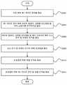
도 3은 본 발명의 일 실시예에 따른 산화물 반도체 트랜지스터의 제조 방법의 전체적인 흐름을 도시한 도면이다.
도 4는 본 발명의 일 실시예에 따른 산화물 반도체 트랜지스터에 있어서, 제2 게이트 전극의 폭이 제1 게이트 전극 및 소스 전극과 드레인 전극 사이의 폭 보다 긴 산화물 반도체 트랜지스터와, 제2 게이트 전극의 폭이 제1 게이트 전극 및 소스 전극과 드레인 전극 사이의 폭 보다 짧은 산화물 반도체 트랜지스터의 구조를 비교한 도면이다.
도 5는 본 발명의 일 실시예에 따라서, LCD 패널과 AMOLED 패널에 적용할 경우를 보여주는 모식도를 도시한 도면이다.
도 6은 본 발명의 일 실시예에 따른 산화물 반도체 트랜지스터의 전이 특성 곡선(Transfer Curve)의 그래프를 도시한 도면이다.
도 7은 본 발명의 일 실시예에 따른 산화물 반도체 트랜지스터(100)의 드레인 전류 및 문턱전압 값의 그래프를 도시한 도면이다.
도 8은 본 발명의 일 실시예에 따른 산화물 반도체 트랜지스터의 제2 게이트 전극의 길이가 26μm/15μm/12μm/6μm로 제1 게이트 전극 길이와 동일할 때의 전이 특성 곡선(transfer curve) 및 전류 곡선(output curve)의 그래프를 도시한 도면이다.
도 9은 본 발명의 일 실시예에 따른 산화물 반도체 트랜지스터의 증가되는 드레인 전류(Increase in)를 상부의 게이트의 사이즈(LTC)에 따라 %로 표현한 그래프를 도시한 도면이다.
도 10 및 도 11은 도 10은 본 발명의 제1 실시예와 제2 실시예의 전기적 특성을 도시한 도면이다.
도 12 및 도 14는 본 발명이 제1 실시예와 제2 실시예에 양의 전압(+20V)의 인가할 때의 전기적 특성을 도시한 도면이다.
도 15 및 도 18은 본 발명이 제1 실시예와 제2 실시예에 음의 전압(-20V/-30V)의 인가할 때의 전기적 특성을 도시한 도면이다.1 is a perspective view of an oxide semiconductor transistor according to an embodiment of the present invention.
2 is a cross-sectional view and an equivalent circuit diagram of an oxide semiconductor transistor according to an embodiment of the present invention.
FIG. 3 is a view showing an overall flow of a method of manufacturing an oxide semiconductor transistor according to an embodiment of the present invention.
FIG. 4 illustrates an oxide semiconductor transistor according to an embodiment of the present invention. In FIG. 4, the width of the second gate electrode is greater than the width of the first gate electrode and the width of the drain electrode. And the structure of the first gate electrode and the oxide semiconductor transistor shorter than the width between the source electrode and the drain electrode.
FIG. 5 is a schematic diagram showing an application to an LCD panel and an AMOLED panel according to an embodiment of the present invention. Referring to FIG.
6 is a graph showing a transfer curve of an oxide semiconductor transistor according to an embodiment of the present invention.
7 is a graph showing a drain current and a threshold voltage value of the
8 is a graph showing a transfer curve and a current curve when the length of the second gate electrode of the oxide semiconductor transistor according to the embodiment of the present invention is 26 mu m / 15 mu m / 12 mu m / (output curve).
9 is a graph showing an increase in drain current (increase in) of an oxide semiconductor transistor according to an embodiment of the present invention expressed as a percentage in accordance with the size (LTC) of the upper gate.
10 and 11 are views showing electrical characteristics of the first embodiment and the second embodiment of the present invention.
Figs. 12 and 14 are diagrams showing electrical characteristics when a positive voltage (+ 20V) is applied to the first embodiment and the second embodiment of the present invention.
FIGS. 15 and 18 are diagrams showing electrical characteristics when negative voltages (-20 V / -30 V) are applied to the first and second embodiments of the present invention.
본 발명은 다양한 변경을 가할 수 있고 여러 가지 실시예를 가질 수 있는 바, 특정 실시예들을 도면에 예시하고 상세한 설명에 상세하게 설명하고자 한다. 그러나, 이는 본 발명을 특정한 실시 형태에 대해 한정하려는 것이 아니며, 본 발명의 사상 및 기술 범위에 포함되는 모든 변경, 균등물 내지 대체물을 포함하는 것으로 이해되어야 한다. 각 도면을 설명하면서 유사한 참조부호를 유사한 구성요소에 대해 사용하였다.While the invention is susceptible to various modifications and alternative forms, specific embodiments thereof are shown by way of example in the drawings and will herein be described in detail. It should be understood, however, that the invention is not intended to be limited to the particular embodiments, but includes all modifications, equivalents, and alternatives falling within the spirit and scope of the invention. Like reference numerals are used for like elements in describing each drawing.
이하에서, 본 발명에 따른 실시예들을 첨부된 도면을 참조하여 상세하게 설명한다.
Hereinafter, embodiments according to the present invention will be described in detail with reference to the accompanying drawings.
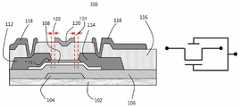
도 1은 본 발명의 일 실시예에 따른 산화물 반도체 트랜지스터의 사시도를 도시한 도면이고, 도 2는 본 발명의 일 실시예에 따른 산화물 반도체 트랜지스터의 단면도 및 등가회로를 도시한 도면이다. 또한, 도 3은 본 발명의 일 실시예에 따른 산화물 반도체 트랜지스터의 제조 방법의 전체적인 흐름을 도시한 도면이다.FIG. 1 is a perspective view of an oxide semiconductor transistor according to an embodiment of the present invention, and FIG. 2 is a cross-sectional view and an equivalent circuit diagram of an oxide semiconductor transistor according to an embodiment of the present invention. FIG. 3 is a flowchart illustrating a method of fabricating an oxide semiconductor transistor according to an embodiment of the present invention. Referring to FIG.
본 발명의 일 실시예에 따른 산화물 반도체 트랜지스터는 디스플레이 장치의 화소 소자로 사용되는, 즉 디스플레이 장치를 구성하는 발광 다이오드를 구동시키기 위해 사용되는 트랜지스터로서, 도 1 및 도 2를 참조하면 산화물 반도체 트랜지스터(100)(이하, "표시 소자용 산화물 반도체 트랜지스터"라고 함)는 기판(102), 제1 게이트 전극(104), 게이트 절연막(106), 산화물 반도체층(108), 에치 스토퍼(110), 소스 전극(112), 드레인 전극(114), 보호층(116), 픽셀 전극(118), 제2 게이트 전극(120) 및 연결 전극(122)을 포함한다.An oxide semiconductor transistor according to an embodiment of the present invention is used as a pixel element of a display device, that is, a transistor used for driving a light emitting diode constituting a display device. Referring to FIGS. 1 and 2, The gate
한편, 표시 소자용 산화물 반도체 트랜지스터(100)는 산화물 반도체 박막 트랜지스터(TFT: Thin Film Transistor)일 수 있다.Meanwhile, the
이하, 도 1 내지 도 3을 참조하여 표시 소자용 산화물 반도체 트랜지스터(100)의 각 구성 요소 별 기능 및 이의 제조 방법에 대해 상세하게 설명한다.Hereinafter, the function of each element of the
먼저, 단계(S302)에서는 기판(102) 위에 제1 게이트 전극(104)을 형성한다.First, in step S302, a
기판(102)은 유리(glass), 플라스틱 또는 석영 재질일 수 있으며, 기판(102)의 위에는 하부 게이트 전극(Bottom Gate)인 제1 게이트 전극(104)이 형성된다.The
그리고, 제1 게이트 전극(104)은 기판(102) 위에 게이트 도전막을 증착하고, 게이트 도전막 상에 포토레지스트 패턴을 형성한 후, 포토레지스트 패턴을 마스크로 하여 게이트 도전막을 선택적으로 식각, 즉, 패터닝함으로써 형성될 수 있다. 제1 게이트 전극(104)은 금속 재질일 수 있으며, 일례로 몰리브덴(Mo)이 사용될 수 있다.The
다음으로, 단계(S304)에서는 제1 게이트 전극 위에 게이트 절연막(Gate Insulator)(106), 산화물 반도체층(108) 및 에치 스토퍼(Etch Stopper)(110)를 순차적으로 형성(증착 및 패터닝)한다.Next, in step S304, a
세부적으로, 제1 게이트 전극(104)의 위에는 게이트 절연막(Gate Insulator)(106)과 산화물 반도체층(108)이 순차적으로 형성(증착 및 패터닝)된다.In detail, a
본 발명의 일 실시예에 따르면, 게이트 절연막(106)은 산화물 또는 금속 산화물일 수 있다. 일례로, 게이트 절연막(106)은 실리콘 산화물(SiO2)일 수 있다.According to one embodiment of the present invention, the
그리고, 본 발명의 일 실시예에 따르면, 산화물 반도체층(108)을 구성하는 물질은 인듐(In)을 포함할 수 있다. 일례로서, 산화물 반도체층(108)을 구성하는 물질은 인듐 갈륨 징크 옥사이드(IGZO), 징크 옥사이드(ZnO), 인듐 징크 옥사이드(IZO), 인듐 틴 옥사이드(ITO), 징크 틴 옥사이드(ZTO), 갈륨 징크 옥사이드(GZO), 하프늄 인듐 징크 옥사이드(HIZO), 징크 인듐 틴 옥사이드(ZITO) 및 알루미늄 징크 틴 옥사이드(AZTO) 중 어느 하나를 포함하여 형성된 비정질 혹은 다결정질로 구성될 수 있다. 이러한 산화물 반도체층(108)은 게이트 전극(104)의 상부 지점(일례로, 동일 축 상의 지점)에 형성될 수 있다.In addition, according to an embodiment of the present invention, the material of the
또한, 산화물 반도체층(108)의 위에는 에치 스토퍼(110)가 형성된다. 이 때, 에치 스토퍼(110)를 구성하는 물질은 산화물 또는 금속 산화물(일례로, 실리콘 산화물(SiO2))일 수 있다. 이러한 에치 스토퍼(110)는 제1 게이트 전극(104)의 상부 지점(일례로, 동일 축 상의 지점)에 형성될 수 있다.An
계속하여, 단계(S306)에서는 게이트 절연막(106), 산화물 반도체층(108) 및 에치 스토퍼(110)의 위에 소스 전극(112) 및 드레인 전극(114)을 형성한다.Subsequently, in step S306, a
여기서, 소스 전극(112) 및 드레인 전극(114)은 서로 수평한 방향으로 형성된다. 따라서, 도 1 및 도 2에 도시된 바와 같이 에치 스토퍼(110)의 일부는 소스 전극(112)과 드레인 전극(114)의 사이, 즉, 채널 부분에 위치하게 된다. 소스 전극(112) 및 드레인 전극(114)은 금속 재질일 수 있으며, 일례로 몰리브덴(Mo)이 사용될 수 있다.Here, the
이 후, 단계(S308)에서는 소스 전극(112) 및 드레인 전극(114)의 위에 보호층(Passivation Layer)(116)을 형성한다. 일례로, 보호층(116)을 구성하는 물질은 산화물 또는 금속 산화물(일례로, 실리콘 산화물(SiO2)) 일 수 있다.Thereafter, a
다음으로, 단계(S310)에서는 보호층(116)의 위에 픽셀 전극(118)(도 1에서는 도시되지 않음)을 형성한다.Next, in step S310, a pixel electrode 118 (not shown in Fig. 1) is formed on the
픽셀 전극(118)은 소스 전극(112) 및 드레인 전극(114)과 각각 전기적으로 연결되며, 소스 전극(112) 및 드레인 전극(114)을 표시 소자용 산화물 반도체 트랜지스터(100) 외부의 다른 구성 요소와 전기적으로 연결시키는 역할을 수행한다. 픽셀 전극(118) 역시 금속 재질, 일례로 몰리브덴(Mo)이 사용될 수 있다.The
마지막으로, 단계(S312)에서는 보호층(116)의 위에 제2 게이트 전극(120) 및 연결 전극(122)을 형성한다.Finally, in step S312, a
상부 게이트 전극(Top Gate)인 제2 게이트 전극(120)은 빛을 차단할 수 있는 금속 재질 또는 빛을 투과할 수 있는 투명한 금속 재질의 전극으로서, 단면도 상에서, 제1 게이트 전극(104)의 상부 지점(일례로, 동일 축 상의 상부 지점)과 대응되는 보호층(116)의 위에 위치한다. 따라서, 제1 게이트 전극(104)의 상부 지점에는 에치 스토퍼(110) 및 제2 게이트 전극(120)이 순차적으로 위치할 수 있다.The
또한, 연결 전극(122)은 제1 게이트 전극(104)와 제2 게이트 전극(120)을 전기적으로 연결하기 위한 전극이다. 따라서, 연결 전극(122)을 통해 제1 게이트 전극(104)과 제2 게이트 전극(120)에는 동일한 전압이 인가될 수 있다.The
그리고, 본 발명의 일 실시예에 따르면, 제1 게이트 전극(104)과 제2 게이트 전극(120)은 동일 축 상에 위치한다. 그리고, 평면도 상에서, 제2 게이트 전극(120)는 제1 게이트 전극(104)과 오버랩될 수 있고, 소스 전극(112)와 드레인 전극(114)의 사이의 공간에 제2 게이트 전극(120)이 놓일 수 있게 된다. 또한, 단면도 상에서, 제2 게이트 전극(120)의 폭은 제1 게이트 전극(104)의 폭 보다 짧을 수 있으며, 제2 게이트 전극(120)의 폭은 소스 전극(112)과 드레인 전극(114) 사이의 폭(즉, 서로 수평한 방향으로 형성된, 소스 전극(112)의 일단과 드레인 전극(114)의 일단의 채널 부분의 폭) 보다 짧을 수 있다.According to an embodiment of the present invention, the
세부적으로, 도 4에서는 제2 게이트 전극(120)의 폭이 제1 게이트 전극(104) 및 소스 전극(112)과 드레인 전극(114) 사이의 폭 보다 "긴" 산화물 반도체 트랜지스터(100)(도 4의 (a) 참조)와, 제2 게이트 전극(120)의 폭이 제1 게이트 전극(104) 및 소스 전극(112)과 드레인 전극(114) 사이의 폭 보다 "짧은" 산화물 반도체 트랜지스터(100)(도 4의 (b) 참조)의 구조를 비교한 도면이다. 도 4에서, 소스 전극(112)과 드레인 전극(114) 사이의 폭은 15μm로 가정하였다.4, the width of the
도 4의 (a)를 참조하면, 제2 게이트 전극(120)의 폭이 제1 게이트 전극(104) 및 소스 전극(112)과 드레인 전극(114) 사이의 폭 보다 "긴" 산화물 반도체 트랜지스터(100)의 경우, 제2 게이트 전극(120)과 소스 전극(112)/드레인 전극(114) 사이에는 기생 전압이 발생하게 되며, 이는 고성능의 전기적 특성을 가지는 산화물 반도체 트랜지스터의 특성이 열화되는 단점을 발생시킨다.4A, the width of the
그러나, 도 4의 (b)를 참조하면, 제2 게이트 전극(120)의 길이 조절을 통해 제1 게이트 전극(104) 및 소스 전극(112)과 드레인 전극(114) 사이의 폭 보다 짧은 산화물 반도체 트랜지스터(100)를 제공함으로써, 제2 게이트 전극(120)과 소스 전극(112)/드레인 전극(114) 사이에 기생 전압이 발생하는 것을 최소화할 수 있게 되며, 고성능의 전기적 특성을 얻을 수 있다. 일례로서, 제2 게이트 전극(120)의 폭은 2μm 이상인 것이 바람직하다.4B, the length of the
또한, 도 1 및 도 2를 참조하면, 제2 게이트 전극(120)의 일단과 소스 전극(112) 사이의 수직한 거리의 폭(122) 및 제2 게이트 전극(120)의 타단과 드레인 전극(114) 사이의 수직한 거리의 폭(124) 중 적어도 하나는 0.5μm 이상 5μm 이하의 값을 가질 수 있다. 즉, 제2 게이트(120)는 소스 전극(112)과 드레인 전극(114) 내에 0.5-5μm의 오프셋 구조로 형성된다.1 and 2, a
이와 같이 보호층(118)의 위에 제2 게이트 전극(120)을 위치시키고, 제1 게이트 전극(104) 제2 게이트 전극(120)에 동일한 전압을 인가하는 경우, 산화물 반도체층(108)에 형성되는 채널의 넓이를 증가시킬 수 있고, 이에 따라, 소스 전극(112)/드레인 전극(114)를 통과하는 전류의 양을 증가시킬 수 있게 될 뿐만 아니라, 양의 전압, 음의 전압과 빛에 대한 신뢰성 테스트에서 안정화될 수 있게 된다. 이에 따라, 본 발명에 따른 표시 소자용 산화물 반도체 트랜지스터(100)의 전기적 특성이 향상된다.In the case where the
또한, 제2 게이트 전극(120)과 연결 전극(122)을 동시에 형성함으로써, 제조 공정을 단순화할 수 있으며, 하나의 전극을 통해 2개의 게이트 전극(104, 120)에 동시에 전압을 인가할 수 있게 되어 표시 소자용 산화물 반도체 트랜지스터(100)의 구조를 단순화할 수 있게 된다.In addition, by simultaneously forming the
도 5는 본 발명의 일 실시예에 따라서, LCD 패널(도 5의 (a))과 AMOLED 패널(도 5의 (b))에 적용할 경우를 보여주는 모식도를 도시한 도면이다.5 is a schematic diagram showing a case where the present invention is applied to an LCD panel (FIG. 5 (a)) and an AMOLED panel (FIG. 5 (b)) according to an embodiment of the present invention.
도 5를 참조하면, LCD 패널(도 5의 (a))의 경우, 산화물 반도체 트랜지스터는 1개가 삽입되며, 상부 게이트 전극(제2 게이트 전극(120)) 및 하부 게이트 전극(제1 게이트 전극(104))에 게이트 구동부의 라인과 전기적 연결이 됨을 보여준다.5, an oxide semiconductor transistor is inserted and an upper gate electrode (a second gate electrode 120) and a lower gate electrode (a first gate electrode (a first gate electrode) 104) is electrically connected to the line of the gate driver.
그리고, AMOLED의 경우(도 5의 (b)), 2개의 산화물 반도체 트랜지스터가 삽입된다. 그리고, 스위칭(Switching) 트랜지스터의 경우, 상부 게이트 전극 및 하부 게이트 전극(제2 게이트 전극(120) 및 제1 게이트 전극(104))은 게이트 구동부의 라인과 연결이 되며, 구동(Driving) 트랜지스터의 경우, 상부 게이트 전극 및 하부의 게이트 전극(제2 게이트 전극(120) 및 제1 게이트 전극(104))이 스위칭 트랜지스터의 나머지(상부 게이트 전극 및 하부게이트 전극이 연결된 게이트 구동부의 라인 및 데이터 구동부와 전기적 연결이 된 라인 외 한 부분) 라인 부분과 전기적 연결이 됨을 보여준다.In the case of AMOLED (Fig. 5 (b)), two oxide semiconductor transistors are inserted. In the case of a switching transistor, the upper gate electrode and the lower gate electrode (the
이하, 도 6 내지 도 18를 참조하여 본 발명의 일 실시예에 따른 표시 소자용 산화물 반도체 트랜지스터(100)의 전기적 특성을 보다 상세하게 설명한다.Hereinafter, the electrical characteristics of the
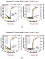
도 6은 본 발명의 일 실시예에 따른 산화물 반도체 트랜지스터(100)의 전이 특성 곡선(Transfer Curve)의 그래프를 도시한 도면이다. 도 6을 참조하면, 산화물 반도체 트랜지스터(100)의 채널폭과 길이(W/L)가 20μm/11μm 및 50μm/11μm에 해당하는 경우, 싱글 게이트의 구조에 비해 전기적 특성이 월등히 향상되었음을 보인다,6 is a graph showing a transfer curve of the
도 7은 본 발명의 일 실시예에 따른 산화물 반도체 트랜지스터(100)의 드레인 전류(도 7의 (a)) 및 문턱전압 값(도 7의 (b))의 그래프를 도시한 도면이다. 도 7를 참조하면, 산화물 반도체 트랜지스터(100)의 채널폭과 길이(W/L)가 20μm/11μm에 해당하는 경우, 싱글 게이트의 구조에 비해 균일성이 높은 결과를 보임을 확인할 수 있다.7 is a graph showing a drain current (FIG. 7A) and a threshold voltage value (FIG. 7B) of an
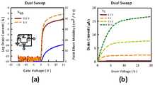
도 8은 본 발명의 일 실시예에 따른 산화물 반도체 트랜지스터(100)의 제2 게이트 전극(120)의 길이가 26μm/15μm/12μm/6μm로 제1 게이트 전극(104) 길이와 동일할 때의 전이 특성 곡선(transfer curve) 및 전류 곡선(output curve)의 그래프를 도시한 도면이다. 도 8을 참조하면, 각각 상부의 게이트(제2 게이트 전극(120))가 floating 상태, Ground (0V), 및 상부 및 하부의 게이트(제1 게이트 전극(104)를 전기적 연결을 하여 측정한 결과를 보여주고 있다.8 is a diagram illustrating a transition of the
도 9은 본 발명의 일 실시예에 따른 산화물 반도체 트랜지스터(100)의 게이트의 전압을 10V, 드레인의 전압이 10V로 인가하여 줄 때, 증가되는 드레인 전류(Increase in)를 상부의 게이트(제2 게이트 전극(120))의 사이즈(LTC)에 따라 %로 표현한 그래프를 도시한 도면이다.9 is a graph showing an increase in drain current (Increase in) applied to the upper gate (the second gate) of the
도 10은 제1 게이트 전극(104)와 제2 게이트 전극(120)이 연결 전극(122)으로 연결되지 않은 본 발명의 제1 실시예의 전기적 특성을 도시한 도면이고, 도 11는 제1 게이트 전극(104)와 제2 게이트 전극(120)이 연결 전극(122)으로 연결된 본 발명의 제2 실시예의 전기적 특성을 도시한 도면이다.10 is a view showing the electrical characteristics of the first embodiment of the present invention in which the
도 10 및 도 11를 참조하면, 본 발명이 제1 실시예와 비교할 때, 본 발명의 제2 실시예가 드레인 전극(114)에 흐르는 전류의 최대치를 더 증가시킬 수 있게 된다.Referring to FIGS. 10 and 11, when the present invention is compared with the first embodiment, the second embodiment of the present invention can further increase the maximum value of the current flowing through the
도 12은 본 발명이 제1 실시예에 양의 전압(+20V)의 인가할 때의 전기적 특성을 도시한 도면이고, 도 13는 본 발명이 제2 실시예에 양의 전압(+20V)의 인가할 때의 전기적 특성을 도시한 도면이며, 도 14는 본 발명이 제1 실시예 및 본 발명이 제2 실시예의 신뢰성 측정 후의 문턱전압의 변화를 비교한 그래프를 도시한 도면이다.FIG. 12 is a graph showing electrical characteristics when a positive voltage (+ 20V) is applied to the first embodiment of the present invention, and FIG. 13 is a graph showing the electrical characteristics when positive voltage FIG. 14 is a graph showing the comparison between the first embodiment of the present invention and the variation of the threshold voltage after the reliability measurement of the second embodiment of the present invention. FIG.
도 12 및 도 14을 참조하면, 본 발명이 제2 실시예가 본 발명이 제1 실시예보다 나은 신뢰성을 가지고 있음을 확인할 수 있다.Referring to FIGS. 12 and 14, it can be seen that the second embodiment of the present invention has better reliability than the first embodiment.
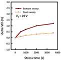
도 15는 본 발명이 제1 실시예에 음의 전압(-20V)의 인가할 때의 전기적 특성을 도시한 도면이고, 도 16는 본 발명이 제2 실시예에 음의 전압(-20V)의 인가할 때의 전기적 특성을 도시한 도면이다. 이 때, 제2 게이트 전극(120)의 일단/타단과 소스 전극(112)/드레인 전극(114)의 수직한 거리 즉, 오프셋은 "1μm (a) / 3μm (b) / 4μm (c) / 5μm (d) / 6μm (e)" 이다.FIG. 15 is a graph showing electrical characteristics when a negative voltage (-20 V) is applied to the first embodiment of the present invention, and FIG. 16 is a graph showing the electrical characteristics of the negative voltage FIG. 5 is a diagram showing electrical characteristics when applied. In this case, the vertical distance between the one end / the other end of the
도 15 및 도 16을 참조하면, 오프셋의 길이가 5μm 이하인 경우 NBIS 신뢰성 테스트에서 좋은 특성을 보이며, 6μm 이상의 경우 NBIS 신뢰성 테스트에서 특성이 변하는 것을 확인할 수 있다.Referring to FIG. 15 and FIG. 16, it can be seen that the characteristic is changed in the NBIS reliability test when the offset length is 5 μm or less, and when the offset length is 6 μm or more.
도 17 및 도 18은 본 발명의 제1 실시예 및 제2 실시예에 강한 음의 전압(-30V)를 인가할 때의 전기적 특성을 도시한 도면이다.17 and 18 are diagrams showing electrical characteristics when a strong negative voltage (-30 V) is applied to the first embodiment and the second embodiment of the present invention.
도 17 및 도 18을 참조하면, 채널의 길이가 길어지면 9000lux의 ILLUMINATION STRESS에 대한 신뢰성이 크게 향상되었음을 확인할 수 있다.Referring to FIGS. 17 and 18, it can be seen that the reliability of the 9,000 lux of ILLUMINATION STRESS is greatly improved when the channel length is increased.
이상과 같이 본 발명에서는 구체적인 구성 요소 등과 같은 특정 사항들과 한정된 실시예 및 도면에 의해 설명되었으나 이는 본 발명의 전반적인 이해를 돕기 위해서 제공된 것일 뿐, 본 발명은 상기의 실시예에 한정되는 것은 아니며, 본 발명이 속하는 분야에서 통상적인 지식을 가진 자라면 이러한 기재로부터 다양한 수정 및 변형이 가능하다. 따라서, 본 발명의 사상은 설명된 실시예에 국한되어 정해져서는 아니되며, 후술하는 특허청구범위뿐 아니라 이 특허청구범위와 균등하거나 등가적 변형이 있는 모든 것들은 본 발명 사상의 범주에 속한다고 할 것이다.As described above, the present invention has been described with reference to particular embodiments, such as specific elements, and limited embodiments and drawings. However, it should be understood that the present invention is not limited to the above- Various modifications and variations may be made thereto by those skilled in the art to which the present invention pertains. Accordingly, the spirit of the present invention should not be construed as being limited to the embodiments described, and all of the equivalents or equivalents of the claims, as well as the following claims, belong to the scope of the present invention .
Claims (10)
Translated fromKorean기판;
상기 기판 위에 위치하는 제1 게이트 전극;
상기 제1 게이트 전극 위에 위치하는 소스 전극 및 드레인 전극; 및
상기 소스 전극 및 상기 드레인 전극 위에 위치하는 제2 게이트 전극;을 포함하되,
상기 제2 게이트 전극의 일단과 상기 소스 전극 사이의 수직한 거리의 폭 및 상기 제2 게이트 전극의 타단과 상기 드레인 전극 사이의 수직한 거리의 폭 중 적어도 하나를 의미하는 오프셋은 0.5μm 이상 5μm 이하의 값을 가지는 것을 특징으로 하는 산화물 반도체 트랜지스터.An oxide semiconductor transistor used as a pixel element of a display device,
Board;
A first gate electrode located on the substrate;
A source electrode and a drain electrode positioned on the first gate electrode; And
And a second gate electrode located above the source electrode and the drain electrode,
An offset which means at least one of a width of a vertical distance between one end of the second gate electrode and the source electrode and a width of a vertical distance between the other end of the second gate electrode and the drain electrode is 0.5 μm or more and 5 μm or less Of the oxide semiconductor layer.
상기 제1 게이트 전극과 상기 제2 게이트 전극은 전기적으로 연결되어 동일한 전압을 인가받는 것을 특징으로 하는 산화물 반도체 트랜지스터.The method according to claim 1,
Wherein the first gate electrode and the second gate electrode are electrically connected to receive the same voltage.
상기 산화물 반도체 트랜지스터는, 상기 제1 게이트 전극과 상기 제2 게이트 전극을 전기적으로 연결하는 연결전극;을 더 포함하는 것을 특징으로 하는 산화물 반도체 트랜지스터.The method according to claim 1,
Wherein the oxide semiconductor transistor further comprises a connection electrode electrically connecting the first gate electrode and the second gate electrode.
상기 산화물 반도체 트랜지스터는,
상기 제1 게이트 전극과 상기 소스 전극 및 드레인 전극 사이에 위치하는 게이트 절연막;
상기 게이트 절연막과 상기 소스 전극 및 상기 드레인 전극 사이에 위치하는 산화물 반도체층; 및
상기 소스 전극 및 상기 드레인 전극과 상기 제2 게이트 전극 사이에 위치하는 보호층;을 더 포함하는 것을 특징으로 하는 산화물 반도체 트랜지스터.The method according to claim 1,
The oxide semiconductor transistor includes:
A gate insulating film positioned between the first gate electrode and the source electrode and the drain electrode;
An oxide semiconductor layer positioned between the gate insulating layer and the source electrode and the drain electrode; And
And a protective layer located between the source electrode and the drain electrode and the second gate electrode.
상기 소스 전극과 상기 드레인 전극은 수평 방향으로 위치하되,
상기 산화물 반도체 트랜지스터는 적어도 일부가 상기 소스 전극과 상기 드레인 전극 사이에 위치하는 에치 스토퍼;를 더 포함하는 것을 특징으로 산화물 반도체 트랜지스터.5. The method of claim 4,
Wherein the source electrode and the drain electrode are positioned in a horizontal direction,
Wherein the oxide semiconductor transistor further comprises an etch stopper at least a part of which is positioned between the source electrode and the drain electrode.
상기 게이트 절연막, 상기 에치 스토퍼, 상기 보호층 중 적어도 하나는 산화물 또는 금속 산화물인 것을 특징으로 하는 산화물 반도체 트랜지스터.6. The method of claim 5,
Wherein at least one of the gate insulating film, the etch stopper, and the protective layer is an oxide or a metal oxide.
상기 산화물 반도체층은 인듐 갈륨 징크 옥사이드(IGZO), 징크 옥사이드(ZnO), 인듐 징크 옥사이드(IZO), 인듐 틴 옥사이드(ITO), 징크 틴 옥사이드(ZTO), 갈륨 징크 옥사이드(GZO), 하프늄 인듐 징크 옥사이드(HIZO), 징크 인듐 틴 옥사이드(ZITO) 및 알루미늄 징크 틴 옥사이드(AZTO) 중 어느 하나를 포함하여 형성된 비정질 혹은 다결정질로 구성되는 것을 특징으로 하는 산화물 반도체 트랜지스터.The method according to claim 1,
The oxide semiconductor layer may include at least one of indium gallium oxide (IGZO), zinc oxide (ZnO), indium zinc oxide (IZO), indium tin oxide (ITO), zinc tin oxide (ZTO), gallium zinc oxide (GZO), hafnium indium zinc Characterized in that the oxide semiconductor transistor is formed of amorphous or polycrystalline material including any one of oxide (HIZO), zinc indium tin oxide (ZITO) and aluminum zinc tin oxide (AZTO).
기판;
상기 기판 위에 위치하는 제1 게이트 전극;
상기 제1 게이트 전극 위에 위치하는 소스 전극 및 드레인 전극; 및
상기 소스 전극 및 상기 드레인 전극 위에 위치하는 제2 게이트 전극;을 포함하되,
상기 제1 게이트 전극과 상기 제2 게이트 전극은 동일 축 상에 위치하고, 상기 제2 게이트 전극의 폭은 상기 제1 게이트 전극의 폭 보다 짧으며, 상기 제1 게이트 전극과 상기 제2 게이트 전극은 전기적으로 연결되어 동일한 전압을 인가받으며, 상기 제2 게이트 전극의 일단과 상기 소스 전극 사이의 수직한 거리의 폭 및 상기 제2 게이트 전극의 타단과 상기 드레인 전극 사이의 수직한 거리의 폭 중 적어도 하나를 의미하는 오프셋은 0.5μm 이상 5μm 이하의 값을 가지는 것을 특징으로 하는 산화물 반도체 트랜지스터.An oxide semiconductor transistor used as a pixel element of a display device,
Board;
A first gate electrode located on the substrate;
A source electrode and a drain electrode positioned on the first gate electrode; And
And a second gate electrode located above the source electrode and the drain electrode,
The first gate electrode and the second gate electrode are located on the same axis, the width of the second gate electrode is shorter than the width of the first gate electrode, and the first gate electrode and the second gate electrode are electrically At least one of a width of a vertical distance between one end of the second gate electrode and the source electrode and a width of a vertical distance between the other end of the second gate electrode and the drain electrode, Wherein the mean offset has a value of 0.5 占 퐉 or more and 5 占 퐉 or less.
상기 제2 게이트 전극의 폭은 상기 소스 전극과 상기 드레인 전극 사이의 폭 보다 짧은 것을 특징으로 하는 산화물 반도체 트랜지스터.9. The method of claim 8,
And the width of the second gate electrode is shorter than the width between the source electrode and the drain electrode.
기판 위에 제1 게이트 전극을 형성하는 단계;
상기 제1 게이트 전극 위에 게이트 절연막, 산화물 반도체층 및 에치 스토퍼를 순차적으로 형성하는 단계;
상기 게이트 절연막, 상기 산화물 반도체층 및 상기 에치 스토퍼의 위에 소스 전극/드레인 전극을 형성하는 단계;
상기 소스 전극/드레인 전극 위에 보호층을 형성하는 단계; 및
상기 보호층의 위에 제2 게이트 전극 및 상기 제1 게이트 전극과 상기 제2 게이트 전극을 전기적으로 연결하는 연결 전극을 형성하는 단계;를 포함하되,
상기 제2 게이트 전극의 일단과 상기 소스 전극 사이의 수직한 거리의 폭 및 상기 제2 게이트 전극의 타단과 상기 드레인 전극 사이의 수직한 거리의 폭 중 적어도 하나를 의미하는 오프셋은 0.5μm 이상 5μm 이하의 값을 가지는 것을 특징으로 하는 산화물 반도체 트랜지스터의 제조 방법.A method of manufacturing an oxide semiconductor transistor used as a pixel element of a display device,
Forming a first gate electrode over the substrate;
Sequentially forming a gate insulating layer, an oxide semiconductor layer, and an etch stopper on the first gate electrode;
Forming a source electrode / drain electrode on the gate insulating layer, the oxide semiconductor layer, and the etch stopper;
Forming a protective layer on the source electrode / drain electrode; And
Forming a second gate electrode on the protection layer and a connection electrode electrically connecting the first gate electrode and the second gate electrode,
An offset which means at least one of a width of a vertical distance between one end of the second gate electrode and the source electrode and a width of a vertical distance between the other end of the second gate electrode and the drain electrode is 0.5 μm or more and 5 μm or less Of the oxide semiconductor layer.
Priority Applications (4)
| Application Number | Priority Date | Filing Date | Title |
|---|---|---|---|
| KR1020130153421AKR101506098B1 (en) | 2013-12-10 | 2013-12-10 | Oxide semiconductor transistor without threshold voltage change in nbis method for manufacturing the same |
| CN201480033487.1ACN105324848A (en) | 2013-06-11 | 2014-05-12 | Oxide semiconductor transistor as pixel element of display device and manufacturing method thereof |
| PCT/KR2014/004232WO2014200190A1 (en) | 2013-06-11 | 2014-05-12 | Oxide semiconductor transistor used as pixel element of display device and manufacturing method therefor |
| US14/965,059US9825058B2 (en) | 2013-06-11 | 2015-12-10 | Oxide semiconductor transistor used as pixel element of display device and manufacturing method therefor |
Applications Claiming Priority (1)
| Application Number | Priority Date | Filing Date | Title |
|---|---|---|---|
| KR1020130153421AKR101506098B1 (en) | 2013-12-10 | 2013-12-10 | Oxide semiconductor transistor without threshold voltage change in nbis method for manufacturing the same |
Publications (1)
| Publication Number | Publication Date |
|---|---|
| KR101506098B1true KR101506098B1 (en) | 2015-03-26 |
Family
ID=53028613
Family Applications (1)
| Application Number | Title | Priority Date | Filing Date |
|---|---|---|---|
| KR1020130153421AActiveKR101506098B1 (en) | 2013-06-11 | 2013-12-10 | Oxide semiconductor transistor without threshold voltage change in nbis method for manufacturing the same |
Country Status (1)
| Country | Link |
|---|---|
| KR (1) | KR101506098B1 (en) |
Cited By (2)
| Publication number | Priority date | Publication date | Assignee | Title |
|---|---|---|---|---|
| KR101842796B1 (en)* | 2016-11-02 | 2018-03-28 | 경희대학교 산학협력단 | Oxide semiconductor transistor having dual gate structure and method of manufacturing the same |
| US12367822B2 (en) | 2023-04-12 | 2025-07-22 | Samsung Display Co., Ltd. | Display device |
Citations (4)
| Publication number | Priority date | Publication date | Assignee | Title |
|---|---|---|---|---|
| KR20090084642A (en)* | 2008-02-01 | 2009-08-05 | 삼성전자주식회사 | Oxide Semiconductor Transistors and Manufacturing Method Thereof |
| JP2010123938A (en)* | 2008-10-24 | 2010-06-03 | Semiconductor Energy Lab Co Ltd | Semiconductor device and method of manufacturing the same |
| JP2010153828A (en)* | 2008-11-21 | 2010-07-08 | Semiconductor Energy Lab Co Ltd | Semiconductor device, and manufacturing method thereof |
| KR20120070709A (en)* | 2010-12-22 | 2012-07-02 | 경희대학교 산학협력단 | Oxide semiconductor inverter using depletion mode of dual gate thin film transistor |
- 2013
- 2013-12-10KRKR1020130153421Apatent/KR101506098B1/enactiveActive
Patent Citations (4)
| Publication number | Priority date | Publication date | Assignee | Title |
|---|---|---|---|---|
| KR20090084642A (en)* | 2008-02-01 | 2009-08-05 | 삼성전자주식회사 | Oxide Semiconductor Transistors and Manufacturing Method Thereof |
| JP2010123938A (en)* | 2008-10-24 | 2010-06-03 | Semiconductor Energy Lab Co Ltd | Semiconductor device and method of manufacturing the same |
| JP2010153828A (en)* | 2008-11-21 | 2010-07-08 | Semiconductor Energy Lab Co Ltd | Semiconductor device, and manufacturing method thereof |
| KR20120070709A (en)* | 2010-12-22 | 2012-07-02 | 경희대학교 산학협력단 | Oxide semiconductor inverter using depletion mode of dual gate thin film transistor |
Cited By (5)
| Publication number | Priority date | Publication date | Assignee | Title |
|---|---|---|---|---|
| KR101842796B1 (en)* | 2016-11-02 | 2018-03-28 | 경희대학교 산학협력단 | Oxide semiconductor transistor having dual gate structure and method of manufacturing the same |
| WO2018084421A1 (en)* | 2016-11-02 | 2018-05-11 | 경희대학교산학협력단 | Oxide semiconductor transistor with dual gate structure and method for manufacturing same |
| US11107927B2 (en) | 2016-11-02 | 2021-08-31 | University-Industry Cooperation Group Of Kyung Hee University | Oxide semiconductor transistor having dual gate structure and method of fabricating the same |
| US11843057B2 (en) | 2016-11-02 | 2023-12-12 | University-Industry Cooperation Group Of Kyung Hee University | Oxide semiconductor transistor having dual gate structure and method of fabricating the same |
| US12367822B2 (en) | 2023-04-12 | 2025-07-22 | Samsung Display Co., Ltd. | Display device |
Similar Documents
| Publication | Publication Date | Title |
|---|---|---|
| US9825058B2 (en) | Oxide semiconductor transistor used as pixel element of display device and manufacturing method therefor | |
| CN103872259B (en) | Double gate type thin film transistors and the organic light emitting diode display including it | |
| US9653484B2 (en) | Array substrate and manufacturing method thereof, display device, thin-film transistor (TFT) and manufacturing method thereof | |
| US10062789B2 (en) | Thin film transistor and operating method thereof | |
| US20110220878A1 (en) | Thin film transistor and method of manufacturing the same | |
| TWI569421B (en) | Pixel structure and method of making the same | |
| KR102281848B1 (en) | Thin film transistor and method of manufacturing the same | |
| US20120146029A1 (en) | Thin film transistor array panel | |
| US9793300B2 (en) | Thin film transistor and circuit structure | |
| CN111146212B (en) | Semiconductor substrate | |
| US10424672B2 (en) | Oxide semiconductor transistor | |
| CN110060998B (en) | Inverter circuit structure, gate drive circuit and display panel | |
| CN104347813A (en) | Transistor, method of manufacturing the transistor, and electronic device including the transistor | |
| KR101506098B1 (en) | Oxide semiconductor transistor without threshold voltage change in nbis method for manufacturing the same | |
| EP3754637B1 (en) | Pixel unit, array substrate and display device | |
| KR101829805B1 (en) | Oxide semiconductor transistor and manufacturing the same | |
| KR20140144566A (en) | Oxide semiconductor transistor used for pixel element of display device and method for manufacturing the same | |
| CN107112365A (en) | Semiconductor device | |
| US20180356660A1 (en) | Active matrix substrate and liquid crystal display panel provided with same | |
| TWI518430B (en) | Display panel and display device using the same | |
| CN104465784A (en) | Thin film transistor and display panel | |
| KR101413656B1 (en) | Transistors and How They Work | |
| CN104681564A (en) | Display panel and display device using same | |
| US20200301182A1 (en) | Active matrix substrate and liquid crystal display panel comprising same | |
| CN106298952B (en) | A kind of OLED device |
Legal Events
| Date | Code | Title | Description |
|---|---|---|---|
| PA0109 | Patent application | Patent event code:PA01091R01D Comment text:Patent Application Patent event date:20131210 | |
| PA0201 | Request for examination | ||
| PE0902 | Notice of grounds for rejection | Comment text:Notification of reason for refusal Patent event date:20140901 Patent event code:PE09021S01D | |
| E701 | Decision to grant or registration of patent right | ||
| PE0701 | Decision of registration | Patent event code:PE07011S01D Comment text:Decision to Grant Registration Patent event date:20150316 | |
| PR0701 | Registration of establishment | Comment text:Registration of Establishment Patent event date:20150319 Patent event code:PR07011E01D | |
| PR1002 | Payment of registration fee | Payment date:20150319 End annual number:3 Start annual number:1 | |
| PG1601 | Publication of registration | ||
| FPAY | Annual fee payment | Payment date:20180124 Year of fee payment:4 | |
| PR1001 | Payment of annual fee | Payment date:20180124 Start annual number:4 End annual number:4 | |
| PR1001 | Payment of annual fee | Payment date:20190123 Start annual number:5 End annual number:5 | |
| FPAY | Annual fee payment | Payment date:20200203 Year of fee payment:6 | |
| PR1001 | Payment of annual fee | Payment date:20200203 Start annual number:6 End annual number:6 | |
| PR1001 | Payment of annual fee | Payment date:20210104 Start annual number:7 End annual number:7 | |
| PR1001 | Payment of annual fee | Payment date:20220221 Start annual number:8 End annual number:8 | |
| PR1001 | Payment of annual fee | Payment date:20230103 Start annual number:9 End annual number:9 |