KR101502759B1 - Data transmitting device, data receiving device and data transmitting method - Google Patents
Data transmitting device, data receiving device and data transmitting methodDownload PDFInfo
- Publication number
- KR101502759B1 KR101502759B1KR1020120032855AKR20120032855AKR101502759B1KR 101502759 B1KR101502759 B1KR 101502759B1KR 1020120032855 AKR1020120032855 AKR 1020120032855AKR 20120032855 AKR20120032855 AKR 20120032855AKR 101502759 B1KR101502759 B1KR 101502759B1
- Authority
- KR
- South Korea
- Prior art keywords
- signal
- current
- data
- binary value
- state
- Prior art date
- Legal status (The legal status is an assumption and is not a legal conclusion. Google has not performed a legal analysis and makes no representation as to the accuracy of the status listed.)
- Expired - Fee Related
Links
Images


Classifications
- H—ELECTRICITY
- H03—ELECTRONIC CIRCUITRY
- H03K—PULSE TECHNIQUE
- H03K19/00—Logic circuits, i.e. having at least two inputs acting on one output; Inverting circuits
- H03K19/0175—Coupling arrangements; Interface arrangements
- G—PHYSICS
- G06—COMPUTING OR CALCULATING; COUNTING
- G06F—ELECTRIC DIGITAL DATA PROCESSING
- G06F30/00—Computer-aided design [CAD]
- G06F30/30—Circuit design
- G06F30/35—Delay-insensitive circuit design, e.g. asynchronous or self-timed
- H—ELECTRICITY
- H04—ELECTRIC COMMUNICATION TECHNIQUE
- H04L—TRANSMISSION OF DIGITAL INFORMATION, e.g. TELEGRAPHIC COMMUNICATION
- H04L25/00—Baseband systems
- H04L25/02—Details ; arrangements for supplying electrical power along data transmission lines
Landscapes
- Engineering & Computer Science (AREA)
- Computer Hardware Design (AREA)
- Physics & Mathematics (AREA)
- Theoretical Computer Science (AREA)
- General Engineering & Computer Science (AREA)
- General Physics & Mathematics (AREA)
- Geometry (AREA)
- Evolutionary Computation (AREA)
- Computing Systems (AREA)
- Mathematical Physics (AREA)
- Power Engineering (AREA)
- Computer Networks & Wireless Communication (AREA)
- Signal Processing (AREA)
- Dc Digital Transmission (AREA)
Abstract
Translated fromKoreanDescription
Translated fromKorean본 발명은 데이터 전송 시스템 및 데이터 전송 방법에 관한 것으로서, 구체적으로 지연 무관 데이터 전송방식에 의해 정보를 전달하는 데이터 전송 시스템 및 데이터 전송 방법에 관한 것이다.BACKGROUND OF THE
현재, 집적 회로 시스템은 반도체 공정 기술과 집적 회로 설계 기술의 발전으로 인하여 하나의 칩 단위로 구현되는 시스템-온-칩(System-on-Chip: SoC) 방식으로 주로 설계되고 있다.Currently, integrated circuit systems are mainly designed as a system-on-chip (SoC) system implemented in a single chip unit due to development of semiconductor process technology and integrated circuit design technology.
최근에는 반도체 공정 기술과 집적 회로 설계 기술이 더욱 발달하여 하나의 칩에 집적할 수 있는 소자의 수가 점차 증가하는 추세이다. 이로 인해 하나의 칩에 설계되는 전송 선로의 배선 구조가 더욱 복잡해지고 있다. 따라서, 집적회로 시스템이 SoC 설계 방식을 구현되는 경우, 전송 선로의 수, 전송 선로의 길이 및 각 전송 선로들 간의 간섭에 의한 신호 지연 등은 칩 전체의 올바른 동작을 위하여 매우 중요하게 고려되어야 하는 설계변수들이다.Recently, semiconductor process technology and integrated circuit design technology have been developed more and the number of devices that can be integrated into one chip is gradually increasing. As a result, the wiring structure of the transmission line designed on one chip is becoming more complicated. Therefore, when the integrated circuit system is implemented in the SoC design method, the number of transmission lines, the transmission line length, and the signal delay due to the interference between the transmission lines must be considered very important for proper operation of the entire chip Variables.
한편, SoC 방식으로 구현되는 집적 회로 시스템에 전역 클록을 이용한 동기식 설계 방식이 적용되는 경우, 클록 속도 증가에 따른 클록 스큐(skew)와 지터(jitter) 및 전송 선로 수와 길이 증가에 따른 데이터의 전송 지연 등이 발생한다. 이러한 문제점들은 SoC 방식을 구현되는 집적 회로 시스템에 비동기식 설계 방식을 적용함으로써 해결될 수 있다.Meanwhile, when a synchronous design method using a global clock is applied to an integrated circuit system implemented by a SoC method, clock skew and jitter as the clock speed increases and data transmission due to the increase of the number of transmission lines and the length Delay and the like occur. These problems can be solved by applying an asynchronous design method to an integrated circuit system implementing a SoC method.
비동기식 설계 방식은 전역 클록(global clock)을 사용하지 않고, 지연 시간에 무관한 핸드셰이크 프로토콜(handshake protocol)을 지원하는 지연 무관 (DI: Delay Insensitive) 데이터 전송 방식에 의해 데이터 전송이 수행됨으로써 상기와 같은 동기식 설계 기법에 따른 문제점을 해결할 수 있다. 그러나 이러한 비동기식 설계방식은 전체 회로의 설계가 복잡해지고, 또한, 이러한 비동기식 설계를 위한 CAD툴이 부족하다.The asynchronous design scheme performs data transmission by using a delay insensitive (DI) data transmission scheme that does not use a global clock but supports a handshake protocol independent of a delay time, It is possible to solve problems caused by the same synchronous design technique. However, this asynchronous design approach complicates the design of the entire circuit, and also lacks CAD tools for such asynchronous design.
상술한 바와 같은 동기식 설계 방식의 문제점과 비동기식 설계방식의 문제점을 동시에 해결할 수 있는 방안으로 최근 GALS(globally asynchronous locally synchronous) 시스템에 대한 연구가 활발히 진행되고 있다.Recently, studies on a globally asynchronous locally synchronous (GALS) system have been actively pursued to solve the problems of the synchronous design method and the asynchronous design method.
GALS 시스템은 기본적으로 전역 클록을 사용하지 않고, 서로 독립적인 클록에 의해 동작하는 다수의 LS(locally synchronous)모듈로 구성된다. 각 LS 모듈 간의 데이터 전송은 비동기 핸드셰이크 프로토콜에 의해 수행된다.The GALS system basically consists of a number of LS (locally synchronous) modules that operate on independent clocks rather than using global clocks. Data transmission between each LS module is performed by an asynchronous handshake protocol.
이와 같이, GALS 시스템은 전역 클록을 사용하지 않으므로, 클록 스큐, 지터 등의 문제가 해결되며, DI 데이터 전송 방식에 의해 서로 다른 타이밍으로 동작하는 LS 모듈 간의 데이터 전송이 이루어짐으로써, 안정된 데이터 전송이 확보된다.In this way, since the GALS system does not use a global clock, problems such as clock skew and jitter are solved and data transmission between LS modules operating at different timings by the DI data transmission method is performed, do.
DI 데이터 전송방식에서는, 듀얼-레일(dual-rail), 1-of-4와 같은 인코딩 방식에 의해 데이터가 표현되며, 기존의 동기식 설계방식과 유사한 4-위상 핸드 세이킹 프로토콜이 사용된다. 그러나 4-위상 핸드세이킹 프로토콜은 데이터 전송과는 관련이 없는 데이터 유효성을 알려주기 위한 스페이스(space) 상태를 포함해야 하고, 상기 스페이스 상태는 데이터와 동일한 레이턴시(latency)를 가진다. 다이 사이즈(die size) 증가로 인해 길어진 연결(interconnect)를 통한 데이터의 전송이 빈번한 GALS 시스템에서는 4-위상 핸드세이킹 프로토콜 방식보다는 스페이스 상태가 없는 2-위상 핸드세이킹 프로토콜 방식이 더 효율적이다.In the DI data transmission method, data is represented by an encoding method such as dual-rail and 1-of-4, and a 4-phase handshaking protocol similar to the conventional synchronous design method is used. However, the 4-phase handshaking protocol should include a space state for indicating data validity that is not related to data transmission, and the space state has the same latency as the data. In a GALS system where data is transmitted over a long interconnect due to die size increase, a 2-phase handshaking protocol scheme with no space state is more efficient than a 4-phase handshaking protocol scheme.
LEDR(Level-Encoded 2-phase Dual-Rail)로 알려진 듀얼-레일 기반의 2-위상 핸드셰이킹 프로토콜은 두 개의 도선에서 '0'과 '1'의 데이터 전송을 각각 도선의 상태 변환으로 인코딩하는 전통적인 듀얼-레일 기반 2-위상 프로토콜과는 달리, 한 도선은 데이터, 다른 도선은 위상 변화로 인코딩한다. 즉, 한 도선에서는 '0'과 '1'의 데이터를 상태 변환이 아닌 레벨로 인코딩하고, 데이터와 데이터 사이의 구분은 다른 도선의 변화로 구분한다. 결과적으로 두 도선의 XOR 값은 데이터 전송마다 변화하게 되며 이를 감지하여 데이터의 유효성을 판별한다. 데이터의 디코딩이 필요 없으므로 전통적인 듀얼-레일 기반 2-위상 프로토콜에 비해서 성능이 높고 설계 복잡도를 줄일 수 있다. 그러나 N 비트 데이터 전송에 2N+1개의 도선이 필요하므로, 늘어난 도선의 수만큼 성능, 전력 소모, 설계 복잡성 측면에서 불리하다.A dual-rail based two-phase handshaking protocol, known as Level-Encoded 2-phase Dual-Rail (LEDR), encodes the data transmission of '0' and '1' Unlike the traditional dual-rail based two-phase protocol, one conductor encodes data and the other conductor encodes a phase change. That is, one conductor encodes data of '0' and '1' to a level, not a state conversion, and distinguishes between data and data by a change of another conductor. As a result, the XOR values of the two conductors are changed for each data transmission, and the validity of the data is detected by sensing the XOR values. Because no data decoding is required, performance is higher and design complexity is reduced compared to traditional dual-rail based 2-phase protocols. However, since 2N + 1 wires are required for N-bit data transmission, the number of wires is disadvantageous in terms of performance, power consumption, and design complexity.
종래의 데이터 전송 기술 중에는 집적 회로 내의 다수의 기능 블록간에서 하나의 도선을 통해 여러 개의 다른 종류의 신호를 동시에 보냄으로써 배선이 점유하는 면적을 감소시킬 수 있는 신호 전송 기술이 있다. 이 기술에 따르면, 이론적으로 N 비트의 데이터 전송 시 도선 1개에 2^N 개의 삼각 펄스 형태의 전압 치를 인코딩하여 전송, 이를 수신회로에서 감지하여 데이터를 복원함으로써 배선에 필요한 도선의 수를 감소시켜 전체적으로 집적회로의 면적을 줄일 수 있다. 그러나 도선에 인코딩할 수 있는 전압 치의 수가 늘어날수록 복호화해야 하는 논리의 수가 증가하여 수신회로의 복잡도가 크게 증가할 수 있으므로 줄일 수 있는 도선의 수가 한정되어 있다. 그리고 집적회로 내의 공급전압이 낮아지고 있는 추세에서, 상기 종래 기술에서 사용하는 전압을 이용한 다치 논리 회로 기술은 수신 회로에서 전압의 노이즈 마진 특성이 악화될 수 있다. 또한, DI 전송에 필요한 핸드셰이크 프로토콜을 지원하기 위한 기능을 제공하지 않기 때문에 GALS 시스템에 적용할 수 없다.Among the conventional data transmission techniques, there is a signal transmission technique which can reduce the area occupied by the wires by simultaneously sending a plurality of different types of signals through a single lead between a plurality of functional blocks in the integrated circuit. According to this technology, theoretically, when transmitting N bits of data, a voltage value of 2 N triangular pulses is transmitted to one conductor, and the received data is recovered by sensing the voltage value, thereby reducing the number of wires necessary for wiring As a whole, the area of the integrated circuit can be reduced. However, as the number of voltage values that can be encoded in the conductor increases, the number of logic circuits to be decoded increases, which can greatly increase the complexity of the receiving circuit. And, in the trend that the supply voltage in the integrated circuit is lowered, the multi-value logic circuit technique using the voltage used in the above-mentioned prior art can deteriorate the noise margin characteristic of the voltage in the receiving circuit. Also, it can not be applied to the GALS system because it does not provide the function to support the handshake protocol required for DI transmission.
DI 전송을 지원하고, 도선의 수를 줄이기 위해 삼진(ternary) 인코딩 방식을 적용한 프로토콜이 연구되고 있다. 이러한 삼진 인코딩 방식을 적용한 데이터 전송 기술에 따르면 전류 모드 방식의 다치 논리 회로(Multiple Valued Logic Circuit)를 사용하여 공급 전압의 노이즈 마진에 영향을 받지 않으며, 하나의 도선에 3가지의 논리 상태를 표현할 수 있으므로 N 비트의 데이터 전송에 N+1개의 도선으로 회로 설계가 가능하다.A protocol using a ternary encoding scheme has been studied to support DI transmission and reduce the number of leads. According to the data transmission technique employing the third-order encoding method, a current mode multiple valued logic circuit is used, so that it is not influenced by the noise margin of the supply voltage, and three logical states can be expressed on one conductor Therefore, it is possible to design the circuit with N + 1 conductors for data transmission of N bits.
또한, 종래의 전류 모드의 DI 데이터 전송 방식에서 발생하는 높은 정전류 소모 특성을 보완하기 위하여, 새로운 데이터 인코딩 방법을 사용함으로써 대기 상태에서 전력 소모를 획기적으로 줄일 수 있는 기술도 연구되었다.In order to compensate for the high constant current consumption characteristic of the conventional DI mode data transmission method, a technique for drastically reducing power consumption in a standby state by using a new data encoding method has been studied.
그러나 상술한 2가지 전류 모드 회로를 이용한 DI 데이터 전송 방식은 기본적으로 4-위상 데이터 전송 방식을 기반으로 하고 있으므로, LEDR과 같은 2-위상 DI 데이터 전송 방식에 비해 성능이 이론적으로는 1/2로 떨어질 수 있는 단점이 있다.However, since the DI data transmission method using the two current mode circuits described above is basically based on the 4-phase data transmission method, the performance is theoretically 1/2 as compared with the two-phase DI data transmission method such as LEDR There is a drawback that it can fall.
상기와 같은 전류 모드 회로를 이용한 DI 데이터 전송 방식의 단점을 보완하기 위하여, 전류 모드 DI 전송 방식의 2-위상 시그널링(signaling) 기법이 제안되었다. 이 방법의 인코더에서는 현재 입력되는 데이터와 그 다음 데이터를 비교하기 위해, 입력되는 요구 신호와 데이터 신호간의 동기화를 가정하고 데이터 신호에 지연 소자를 삽입하여 그 다음 요구 신호에서 지연된 현재 데이터를 추출한다. 그러나, 비동기식 신호 환경에서 요구 신호보다 데이터 신호가 먼저 안정화되어야 한다라는 동기화 가정만을 가지고 인코더 설계 시에 설계자가 지연 소자의 지연 시간을 정하기 위해 입력 요구 신호와 데이터 신호의 가장 큰 시간 차와 요구 신호의 가장 짧은 주기 시간을 알아야 한다. 이는 지연 소자의 지연 시간을 결정하는 것이 매우 어려울 수 있거나, 어떤 경우(입력 요구 신호와 데이터 신호의 가장 큰 시간 차 > 요구 신호의 가장 짧은 주기 시간)에는 만족하는 지연 소자의 지연 시간을 찾지 못해 인코더의 기능성(functionality)를 보장할 수 없을 수도 있음을 의미한다. 또한, 이 기술의 디코더에서는 데이터 신호를 복원하기 위해 D-플립 플롭을 사용하는데, 이 소자의 데이터 캡쳐 시점, 즉, 이 소자의 클록 신호를 만들어 주는 부가 로직이 필요하다. 그리고, 이 기술에서는 전압 모드 이진 데이터의 전송에서 흔히 사용하는 버퍼 삽입과 같은 긴 도선을 통한 전송 시의 레이턴시를 감소시키는 방법이 제시되지 않았다.In order to compensate for the disadvantages of the DI data transmission method using the current mode circuit, a two-phase signaling method using a current mode DI transmission method has been proposed. The encoder of this method assumes the synchronization between the input request signal and the data signal in order to compare the currently inputted data with the next data and inserts the delay element into the data signal to extract the delayed current data from the next request signal. However, in the asynchronous signal environment, in order to determine the delay time of the delay element at the time of designing the encoder, only the synchronization is assumed that the data signal must be stabilized before the request signal. In designing the encoder, You need to know the short cycle time. It may be very difficult to determine the delay time of the delay element, or in some cases (the greatest time difference between the input request signal and the data signal> the shortest cycle time of the request signal) It may not be possible to guarantee the functionality of the system. In addition, the decoder of this technique uses a D-flip flop to recover the data signal, which requires additional data logic to capture the data, i.e., the clock signal of the device. In addition, this technique does not disclose a method for reducing the latency during transmission through a long conductor, such as buffer insertion, which is often used in transmission of voltage mode binary data.
본 발명의 목적은, 지연 소자를 통한 상태 저장 대신 유한 상태 머신(Finite State Machine; FSM) 로직을 이용함으로써, 요구 신호 및 데이터 신호와 관련한 시간에 대한 가정이 필요없고, 디코더에 클록 신호를 만들어주는 부가 로직이 필요 없어서, 디코더의 회로 구조를 단순화할 수 있는 데이터 송신 장치, 데이터 수신 장치 및 데이터 전송 방법을 제공하는 것이다.It is an object of the present invention to provide a method and apparatus for generating a clock signal to a decoder by using finite state machine (FSM) logic instead of state storage through a delay element, A data transmitting apparatus, a data receiving apparatus, and a data transmitting method that can simplify a circuit structure of a decoder without requiring additional logic.
본 발명의 일 실시예에 따른 데이터 송신 장치는, 요구 신호와, 상기 요구 신호의 천이 시점에 의해 '0'의 이진값 및 '1'의 이진값으로 구분되는 비 복귀 제로(Non-Return-to-Zero; NRZ) 형식의 데이터 신호를 생성하는 데이터 송신기; 및 상기 요구 신호와 상기 데이터 신호를 수신하고, 상기 '0'의 이진값을 나타내는 로우 상태와, 상기 '1'의 이진값을 나타내는 하이 상태와, 이전의 이진값과 동일한 현재의 이진값을 나타내는 미들 상태를 소정의 상태 신호에 할당하여 생성된 유한 상태 머신(Finite State Machine)을 이용하여, 상기 수신한 요구 신호와 상기 데이터 신호를 연산하여, 상기 '0'의 이진값, 상기 '1'의 이진값 및 이전의 이진값과 동일한 현재의 이진값을 서로 다른 전류 레벨로 각각 변환하는 인코더를 포함하여 구성된다.A data transmitting apparatus according to an embodiment of the present invention includes a request signal and a non-return-to zero (" 0 " A data transmitter for generating a data signal in the form of -Zero; NRZ); And a low state indicating a binary value of '0', a high state indicating a binary value of '1', and a current state indicating a current binary value equal to a previous binary value. 0 ', a binary value of' 0 ', a binary value of' 0 ', a binary value of' 0 ', and a binary value of' 0 'by using a finite state machine generated by assigning a middle state to a predetermined state signal, And an encoder for converting the current binary value equal to the binary value and the previous binary value to different current levels, respectively.
상기 서로 다른 전류 레벨은 제1 전류 레벨, 상기 제1 전류 레벨보다 낮은 제2 전류 레벨 및 상기 제1 전류 레벨보다 작고, 상기 제2 전류 레벨보다 큰 제3 전류 레벨을 포함할 수 있고, 상기 인코더는 상기 '1'의 이진값을 전송하는 경우, 상기 제1 전류 레벨을 출력하고, 상기 '0'의 이진값을 전송하는 경우, 상기 제1 전류 레벨보다 작은 제2 전류 레벨을 출력하고, 상기 이전의 이진값과 동일한 상기 현재의 이진값의 데이터 신호를 전송하는 경우, 상기 제1 전류 레벨보다 작고, 상기 제2 전류 레벨보다 큰 제3 전류 레벨을 출력할 수 있다.The different current levels may include a first current level, a second current level lower than the first current level, and a third current level that is less than the first current level and greater than the second current level, Outputs a first current level when the binary value of '1' is transmitted, and outputs a second current level which is smaller than the first current level when transmitting the binary value of '0' When the data signal of the current binary value equal to the previous binary value is transmitted, a third current level lower than the first current level and higher than the second current level may be output.
상기 인코더는, 상기 데이터 신호와 상기 요구 신호를 이용하여, 상기 '0'의 이진값을 나타내는 로우 상태와, 상기 '1'의 이진값을 나타내는 하이 상태와, 이전의 이진값과 동일한 현재의 이진값을 나타내는 미들 상태 중 하나인 현재 상태에 대응하는 상태 신호를 출력하는 데이터 상태 머신; 및 상기 현재 상태에 대응하는 상태 신호에 따라 상기 제1 내지 제3 전류 레벨 중 어느 하나를 출력하는 전류 발생기를 포함할 수 있다.The encoder uses the data signal and the request signal to generate a low state indicating a binary value of '0', a high state indicating a binary value of '1', and a high state indicating a binary state of the current binary A data state machine for outputting a state signal corresponding to a current state which is one of middle states indicating a value; And a current generator for outputting any one of the first to third current levels according to a state signal corresponding to the current state.
본 발명의 다른 실시예에서, 상기 데이터 송신 장치는, 상기 요구 신호, 상기 데이터 신호, 상기 현재 상태에 대응하는 상태 신호 및 데이터 수신 장치에서 복원된 요구 신호와 복원된 데이터 신호에 응답하여 송신된 응답 신호에 기반하여, 충전 펄스 신호 또는 방전 펄스 신호를 생성하는 전류 가감 예측기; 및 상기 충전 펄스 신호 또는 방전 펄스 신호를 수신하여 미리 충전 또는 방전하여 상기 전류 발생기에서 발생하는 전류를 제어하는 전류 가감기를 더 포함할 수 있다.In another embodiment of the present invention, the data transmission apparatus further includes a response signal transmitted in response to the request signal, the data signal, the status signal corresponding to the current status, the request signal reconstructed by the data reception apparatus, A current impulse predictor for generating a charge pulse signal or a discharge pulse signal based on the signal; And a current accelerator for controlling the current generated in the current generator by charging or discharging the charge pulse signal or the discharge pulse signal in advance.
본 발명의 일 실시예에 따른 데이터 수신 장치는, '0'의 이진값을 나타내는 로우 상태와, '1'의 이진값을 나타내는 하이 상태와, 이전의 이진값과 동일한 현재의 이진값을 나타내는 미들 상태를 소정의 상태 신호에 할당하여 생성된 유한 상태 머신(Finite State Machine)을 이용하여 인코딩된 입력 전류 신호를 수신하고, 내부에서 생성된 기준 전류를 이용하여 상기 3가지 논리 상태에 대응하는 전압 값을 생성하고, 상기 생성된 전압 값에 따라 상기 요구 신호와 상기 데이터 신호를 복원하는 디코더; 및 상기 복원된 요구 신호와 상기 복원된 데이터 신호에 응답하여 응답 신호를 상기 송신측에 전송하는 데이터 수신기를 포함하여 구성된다.The data receiving apparatus according to an embodiment of the present invention includes a low state indicating a binary value of '0', a high state indicating a binary value of '1', a middle state indicating a binary value equal to a previous binary value, Receiving an encoded input current signal using a finite state machine generated by assigning a state to a predetermined state signal and outputting a voltage value corresponding to the three logic states using a reference current generated internally A decoder for recovering the request signal and the data signal according to the generated voltage value; And a data receiver for transmitting a response signal to the transmitter in response to the restored request signal and the restored data signal.
상기 복원된 데이터 신호는 상기 복원된 요구 신호의 천이 시점에 의해 '0'의 이진값 및 '1'의 이진값으로 구분되는 비 복귀 제로(Non-Return-to-Zero; NRZ) 형식일 수 있다.The restored data signal may be in a non-return-to-zero (NRZ) format, which is divided into a binary value of '0' and a binary value of '1' depending on the transition timing of the restored request signal .
상기 입력 전류 신호는 상기 하이 상태에 대응하는 제1 전류 레벨, 상기 로우 상태에 대응하는 제2 전류 레벨 및 상기 미들 상태에 대응하는 제3 전류 레벨 중 어느 하나의 전류 레벨로 이루어지고, 상기 제2 전류 레벨은 상기 제1 전류 레벨보다 낮고, 상기 제3 전류 레벨은 상기 제1 전류 레벨보다 낮고, 상기 제2 전류 레벨보다 클 수 있다.Wherein the input current signal comprises one of a first current level corresponding to the high state, a second current level corresponding to the low state, and a third current level corresponding to the middle state, The current level is lower than the first current level and the third current level is lower than the first current level and higher than the second current level.
본 발명의 일 실시예에 따른 데이터 전송 방법은, 요구 신호와, 상기 요구 신호의 천이 시점에 의해 '0'의 이진값 및 '1'의 이진값으로 구분되는 비 복귀 제로(Non-Return-to-Zero; NRZ) 형식의 데이터 신호를 수신하는 단계; 상기 '0'의 이진값을 나타내는 로우 상태와, 상기 '1'의 이진값을 나타내는 하이 상태와, 이전의 이진값과 동일한 현재의 이진값을 나타내는 미들 상태를 소정의 상태 신호에 할당하여 생성된 유한 상태 머신(Finite State Machine)을 이용하여, 상기 수신한 요구 신호와 상기 데이터 신호를 연산하여, 연산된 결과치에 따라 상기 '1'의 이진값을 제1 전류 레벨로 코딩하고, 상기 '0'의 이진값을 상기 제1 전류 레벨보다 낮은 제2 전류 레벨로 코딩하고, 이전의 이진값과 동일한 현재의 이진값을 상기 제1 전류 레벨보다 낮고, 상기 제2 전류 레벨보다 높은 제3 전류 레벨로 코딩하는 단계; 상기 코딩된 제1 내지 제3 전류 레벨 중 어느 하나의 전류 레벨을 수신하는 단계; 상기 수신된 어느 하나의 전류 레벨을 검출하고, 검출된 전류 레벨에 따라 제1 및 제2 논리 전압을 생성하는 단계; 및 상기 제1 및 제2 논리 전압을 연산하여 상기 데이터 신호 및 상기 요구 신호를 복원하는 단계를 포함하여 구성된다.A data transmission method according to an embodiment of the present invention includes a request signal and a non-return-zero (" 0 ") signal, which is divided into a binary value of '0' Receiving a data signal in the form of -Zero; NRZ); And a middle state indicating a current binary value equal to the previous binary value to a predetermined state signal to generate a binary value of '0', a low state indicating a binary value of '0' A binary value of '1' is coded to a first current level according to the computed result, and the binary value of '1' is encoded by using a finite state machine (Finite State Machine) And a current binary value equal to the previous binary value is lower than the first current level and is higher than the second current level by a third current level lower than the first current level Coding; Receiving the current level of any one of the coded first through third current levels; Detecting one of the received current levels and generating first and second logic voltages according to the detected current level; And calculating the first and second logic voltages to restore the data signal and the request signal.
상기 어느 하나의 전류 레벨은 2-위상 지연 무관 데이터 전송 방식에 따라 수신될 수 있다.Either one of the current levels may be received according to a two-phase delay-free data transmission scheme.
본 발명의 일 측면에 따르면, 지연 소자를 통한 상태 저장 대신 유한 상태 머신(Finite State Machine; FSM) 로직을 이용함으로써, 요구 신호 및 데이터 신호와 관련한 시간에 대한 가정이 필요없고, 디코더에 클록 신호를 만들어주는 부가 로직이 필요 없어서, 디코더의 회로 구조를 단순화할 수 있는 데이터 송신 장치, 데이터 수신 장치 및 데이터 전송 방법을 제공할 수 있다.According to an aspect of the present invention, by using finite state machine (FSM) logic instead of state storage through a delay element, it is unnecessary to assume a time in relation to a request signal and a data signal, It is possible to provide a data transmitting apparatus, a data receiving apparatus, and a data transmitting method which can simplify the circuit structure of a decoder.
또한, 본 발명의 다른 측면에 따른 데이터 송신 장치는 입력되는 데이터 신호와 현재 상태 정보로 전류량 가감을 예측함으로써, 긴 도선에서 저항(Resistance), 캐패시턴스(Capacitance) 값에 의한 레이턴시를 감소시킬 수 있다.In addition, the data transmission apparatus according to another aspect of the present invention can reduce the latency due to the resistance and capacitance values on the long conductor by predicting the amount of the added current by the input data signal and the current state information.
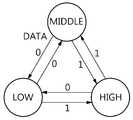
도 1은 본 발명의 일 실시예에 따른 데이터 송신 장치, 데이터 수신 장치 및 데이터 전송 방법에 적용되는 2-위상 3진 인코딩 방식에 따라 인코딩된 값의 논리 상태의 변화를 나타내는 도면이다.
도 2는 본 발명의 일 실시예에 따른 데이터 송신 장치, 데이터 수신 장치 및 데이터 전송 방법에 적용되는 2-위상 3진 인코딩 방식에 따라 인코딩된 값의 일례를 설명하는 도면이다.
도 3은 본 발명의 일 실시예에 따른 데이터 송신 장치 및 데이터 수신 장치의 내부 구성을 나타내는 블록도이다.
도 4는 본 발명의 일 실시예에 따른 데이터 송신 장치의 인코더의 상태 천이 다이어그램이다.
도 5는 본 발명의 일 실시예에 따른 데이터 송신 장치의 인코더의 내부 구성의 일례를 나타내는 회로도이다.
도 6은 본 발명의 일 실시예에 따른 데이터 수신 장치의 디코더의 내부 구성의 일례를 나타내는 회로도이다.
도 7은 긴 도선에서의 인코더 출력 전류 신호의 늘어짐 현상을 설명하기 위한 도면이다.
도 8은 본 발명의 다른 실시예에 따른 데이터 송신 장치의 인코더의 내부 구성의 일례를 나타내는 블록도이다.
도 9는 본 발명의 다른 실시예에 따른 데이터 송신 장치의 인코더의 상태 천이에 따른 전류 충전 또는 방전 동작을 설명하기 위한 상태 천이 다이어그램이다.
도 10은 본 발명의 다른 실시예에 따른 데이터 송신 장치의 인코더의 상태 천이에 따른 전류 충전 또는 방전 동작을 설명하기 위한 인코더 내부 신호들의 타이밍 도이다.
도 11은 본 발명의 다른 실시예에 따른 데이터 송신 장치의 인코더의 전류 가감 예측기의 내부 구성의 일례를 나타내는 회로도이다.
도 12는 본 발명의 다른 실시예에 따른 데이터 송신 장치의 인코더의 전류 가감기의 내부 구성의 일례를 나타내는 회로도이다.1 is a diagram illustrating a change in a logical state of a value encoded according to a two-phase ternary encoding scheme applied to a data transmitting apparatus, a data receiving apparatus, and a data transmitting method according to an embodiment of the present invention.
FIG. 2 is a view for explaining an example of encoded values according to a two-phase ternary encoding scheme applied to a data transmitting apparatus, a data receiving apparatus, and a data transmitting method according to an embodiment of the present invention.
3 is a block diagram showing an internal configuration of a data transmitting apparatus and a data receiving apparatus according to an embodiment of the present invention.
4 is a state transition diagram of an encoder of a data transmitting apparatus according to an embodiment of the present invention.
5 is a circuit diagram showing an example of the internal configuration of an encoder of a data transmitting apparatus according to an embodiment of the present invention.
6 is a circuit diagram showing an example of the internal configuration of a decoder of a data receiving apparatus according to an embodiment of the present invention.
7 is a diagram for explaining a sagging phenomenon of an encoder output current signal in a long conductor.
8 is a block diagram showing an example of the internal configuration of an encoder of a data transmitting apparatus according to another embodiment of the present invention.
9 is a state transition diagram for explaining a current charging or discharging operation according to a state transition of an encoder of a data transmitting apparatus according to another embodiment of the present invention.
10 is a timing chart of internal signals of the encoder for explaining the current charging or discharging operation according to the state transition of the encoder of the data transmitting apparatus according to another embodiment of the present invention.
11 is a circuit diagram showing an example of the internal configuration of a current impulse / predictor of an encoder of a data transmitting apparatus according to another embodiment of the present invention.
12 is a circuit diagram showing an example of an internal configuration of a current add / drop unit of an encoder of a data transmitting apparatus according to another embodiment of the present invention.
본 발명을 첨부된 도면을 참조하여 상세히 설명하면 다음과 같다. 여기서, 반복되는 설명, 본 발명의 요지를 불필요하게 흐릴 수 있는 공지 기능, 및 구성에 대한 상세한 설명은 생략한다. 본 발명의 실시형태는 당 업계에서 평균적인 지식을 가진 자에게 본 발명을 보다 완전하게 설명하기 위해서 제공되는 것이다. 따라서, 도면에서의 요소들의 형상 및 크기 등은 보다 명확한 설명을 위해 과장될 수 있다.
The present invention will now be described in detail with reference to the accompanying drawings. Hereinafter, a repeated description, a known function that may obscure the gist of the present invention, and a detailed description of the configuration will be omitted. Embodiments of the present invention are provided to more fully describe the present invention to those skilled in the art. Accordingly, the shapes and sizes of the elements in the drawings and the like can be exaggerated for clarity.
도 1은 본 발명의 일 실시예에 따른 데이터 송신 장치, 데이터 수신 장치 및 데이터 전송 방법에 적용되는 2-위상 3진 인코딩 방식에 따라 인코딩된 값의 논리 상태의 변화를 나타내는 도면이다.1 is a diagram illustrating a change in a logical state of a value encoded according to a two-phase ternary encoding scheme applied to a data transmitting apparatus, a data receiving apparatus, and a data transmitting method according to an embodiment of the present invention.
도 1을 참조하면, 본 발명의 일 실시예에 따른 데이터 송신 장치, 데이터 수신 장치 및 데이터 전송 방법에 적용되는 2-위상 3진 인코딩 방식에서는 이진값 '0'과 이진값 '1'을 표시하기 위해 데이터 신호가 스페이스(space) 상태가 없는 비 복귀 제로(Non-Return to Zero; NRZ) 방식으로 포맷(format)된다. NRZ 방식으로 포맷된 데이터 신호는 3가지의 논리 상태로 인코딩된다.Referring to FIG. 1, in a two-phase ternary encoding scheme applied to a data transmitting apparatus, a data receiving apparatus, and a data transmitting method according to an embodiment of the present invention, a binary value '0' and a binary value '1' The data signal is formatted in a non-return to zero (NRZ) manner in which there is no space state. A data signal formatted in NRZ format is encoded into three logic states.
예컨대, 이진값 '1'을 전송하는 경우, 데이터 신호는 하이(HIGH) 상태로 인코딩되고, 이진값 '0'을 전송하는 경우, 데이터 신호는 로우(LOW) 상태로 인코딩된다.For example, when transmitting the binary value '1', the data signal is encoded into the HIGH state, and when transmitting the binary value '0', the data signal is encoded into the LOW state.
만일, 이전의 데이터 신호의 이진값과 동일한 현재의 데이터 신호의 이진값을 전송하는 경우, 현재의 데이터 신호는 미들(MIDDLE) 상태로 인코딩된다. 물론, 이진값 '0'을 나타내는 데이터 신호가 하이(HIGH) 상태로 인코딩되고, 이진값 '1'을 나타내는 데이터 신호가 로우(LOW) 상태로 인코딩될 수도 있으나, 본 명세서에서는 이진값 '0'을 나타내는 데이터 신호는 로우(LOW) 상태로 인코딩되고, 이진값 '1'을 나타내는 데이터 신호는 하이(HIGH) 상태로 인코딩되는 것으로 가정한다.If a binary value of the current data signal that is equal to the binary value of the previous data signal is transmitted, the current data signal is encoded into the MIDDLE state. Of course, a data signal representing a binary value '0' may be encoded into a HIGH state and a data signal representing a binary value '1' may be encoded into a LOW state. However, Is encoded into a LOW state, and a data signal representing a binary value '1' is encoded into a HIGH state.
본 발명에서는 상기 3가지의 논리 상태(HIGH, MIDDLE 및 LOW)를 나타내는 인코딩된 값(Encoded Value)들은 수신측으로 전송되기 위해 서로 다른 3가지 전류 레벨로 각각 변환된다. 예컨대, 상기 하이(HIGH) 상태는 제1 전류 레벨로 표현되고, 상기 로우(LOW) 상태는 상기 제1 전류 레벨보다 작은 제2 전류 레벨로 표현된다. 상기 미들(MIDDLE) 상태는 상기 제1 전류 레벨보다 작고, 상기 제2 전류 레벨보다 큰 제3 전류 레벨로 표현된다. 여기서, 이진값 '0'을 나타내는 데이터 신호가 하이 상태로 인코딩되고, 이진값 '1'을 나타내는 데이터 신호가 로우(LOW) 상태로 인코딩되는 경우, 상기 이진값 '0'을 나타내는 데이터 신호는 상기 제1 전류 레벨로 변환되고, 상기 이진값 '1'을 나타내는 데이터 신호는 상기 제3 전류 레벨로 변환될 수도 있다.In the present invention, the encoded values representing the above three logic states (HIGH, MIDDLE and LOW) are respectively converted into three different current levels for transmission to the receiver side. For example, the HIGH state is represented by a first current level, and the LOW state is represented by a second current level that is less than the first current level. The MIDDLE state is represented by a third current level that is smaller than the first current level and greater than the second current level. Here, when a data signal representing a binary value '0' is encoded into a high state and a data signal representing a binary value '1' is encoded into a low state, a data signal representing the binary value '0' The data signal representing the binary value '1' may be converted to the first current level, and the data signal representing the binary value '1' may be converted to the third current level.
본 발명의 일 실시예에 따른 데이터 송신 장치, 데이터 수신 장치 및 데이터 전송 방법에 적용되는 2-위상 3진 인코딩 방식은 종래의 4-위상 3진 인코딩 방식과는 달리 스페이스(space) 상태가 없으므로, 적은 수의 신호 변환으로 데이터 신호를 전송할 수 있다.
Since the two-phase ternary encoding method applied to the data transmitting apparatus, the data receiving apparatus, and the data transmitting method according to the embodiment of the present invention does not have a space state unlike the conventional 4-phase ternary encoding method, The data signal can be transmitted with a small number of signal conversions.
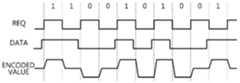
도 2는 본 발명의 일 실시예에 따른 데이터 송신 장치, 데이터 수신 장치 및 데이터 전송 방법에 적용되는 2-위상 3진 인코딩 방식에 따라 인코딩된 값의 일례를 설명하는 도면이다.FIG. 2 is a view for explaining an example of encoded values according to a two-phase ternary encoding scheme applied to a data transmitting apparatus, a data receiving apparatus, and a data transmitting method according to an embodiment of the present invention.
도 2를 참조하면, 본 발명의 일 실시예에 따른 데이터 송신 장치, 데이터 수신 장치 및 데이터 전송 방법에 적용되는 2-위상 3진 인코딩 방식에 따라 인코딩된 값은 2-위상 번들 데이터(2-phase bundled data) 전송 방식에 따라 수신 측으로 전송된다.Referring to FIG. 2, a value encoded according to a 2-phase ternary encoding scheme applied to a data transmitting apparatus, a data receiving apparatus, and a data transmitting method according to an embodiment of the present invention includes 2-phase bundle data 2-phase and is transmitted to the receiving side according to the bundled data transmission method.
본 발명의 일 실시예에 따른 데이터 송신 장치, 데이터 수신 장치 및 데이터 전송 방법에서 사용되는 상기 2-위상 번들 데이터 전송 방식에서는, 도 2에 도시된 바와 같이, 상기 데이터 신호(DATA)와 더불어 상기 데이터 신호(DATA)의 '1'의 이진값 및 '0'의 이진값을 추출하기 위한 요구 신호(REQ)가 필요하다. 즉, 상기 요구 신호(REQ)의 천이시점을 기준으로 상기 데이터 신호(DATA)는 '1'의 이진값 및 '0'의 이진값으로 추출된다. 결과적으로, 번들 데이터 전송 방식에서는 데이터 신호(DATA)를 샘플링하기 위한 요구 신호(REQ)가 필요하다.In the two-phase bundle data transmission method used in the data transmitting apparatus, the data receiving apparatus, and the data transmitting method according to the embodiment of the present invention, as shown in FIG. 2, in addition to the data signal DATA, A request signal REQ for extracting a binary value of '1' and a binary value of '0' of the signal DATA is required. That is, the data signal DATA is extracted as a binary value of '1' and a binary value of '0' based on a transition point of the request signal REQ. As a result, in the bundled data transmission system, a request signal REQ for sampling the data signal DATA is required.
상기 데이터 신호(DATA)가 수신 측에 안정적으로 전송되기 위해서는 상기 요구 신호(REQ)에 의해 안정적으로 샘플링되어야 한다. 따라서, 상기 번들 데이터 전송 방식에서는 도 2에 도시된 바와 같이, 데이터 신호(DATA)가 먼저 안정화된 이후에 요구 신호(REQ)가 발생한다(assert). 즉, 상기 데이터 신호(DATA)의 라이징(rising) 시점이 요구 신호(REQ)의 상승 시점보다 빠르게 설정된다.In order for the data signal DATA to be stably transmitted to the receiving side, it must be stably sampled by the request signal REQ. Therefore, in the bundle data transmission method, as shown in FIG. 2, a request signal REQ is asserted after the data signal DATA is stabilized first. That is, the rising time of the data signal DATA is set earlier than the rising time of the request signal REQ.
도 2에서는 연속된 일련의 데이터 신호(1 1 0 0 1 0 1 0 0 1)와 상기 요구 신호(REQ)를 이용하여 2-위상 번들 데이터(2-phase bundled data) 전송 방식 환경에서 인코딩된 값(Encoded Value)의 일례가 나타난다.In FIG. 2, a value encoded in a 2-phase bundled data transmission environment using a continuous series of data signals (1 1 0 0 1 0 1 0 0 1) and the request signal (REQ) (Encoded Value).
도 1에서 설명한 바와 같이, 인코딩된 값(Encoded Value)이 하이(HIGH) 상태인 경우, 이진값 '1'을 나타내는 데이터 신호(DATA)가 제1 전류 레벨("2I")로서 수신 측으로 전송되고, 로우(LOW) 상태인 경우, 이진값 '0'을 나타내는 데이터 신호(DATA)는 상기 제1 전류 레벨("2I")보다 낮은 제2 전류 레벨("I")로서 수신 측으로 전송된다.1, when the encoded value is in the HIGH state, the data signal DATA indicating the binary value '1' is transmitted to the receiving side as the first current level ("2I") , The data signal DATA indicating the binary value '0' is transmitted to the receiving side as a second current level ("I") lower than the first current level ("2I").
또한, 인코딩된 값(Encoded Value)이 미들(MIDDLE) 상태인 경우, 이전의 이진값과 동일한 이진값을 나타내는 데이터 신호(DATA)가 상기 제1 전류 레벨("2I")보다 낮고, 상기 제2 전류 레벨("O")보다 높은 제3 전류 레벨("I")로서 상기 수신 측으로 전송된다.When the encoded value is in the MIDDLE state, the data signal DATA indicating the same binary value as the previous binary value is lower than the first current level ("2I"), Is transmitted to the receiving side as a third current level ("I") higher than the current level ("O").
이와 같이, 본 발명에서는 3진 인코딩 방식을 구현하기 위하여 3가지 상태(HIGH, MIDDLE 및 LOW)를 서로 다른 전류 레벨로 각각 변환하여 수신 측으로 전송한다. 따라서, 본 발명에서는 상기 3가지 상태(HIGH, MIDDLE 및 LOW)를 서로 다른 전류 레벨로 각각 변환하는 전류 모드 방식의 다치 논리 회로(Multiple Valued Logic Circuit)가 채용된다.As described above, in order to implement the ternary encoding scheme, the present invention converts three states (HIGH, MIDDLE, and LOW) into different current levels and transmits them to the receiver. Therefore, in the present invention, a multiple valued logic circuit of a current mode scheme is used, which converts the three states (HIGH, MIDDLE and LOW) into different current levels.
다치 논리 회로는 전압 모드 방식과 본 발명에서 채용되는 전류 모드 방식이 있다.The multi-value logic circuit has a voltage mode mode and a current mode mode employed in the present invention.
만일, 전압 모드 방식의 다치 논리 회로가 본 발명에서 채용되는 경우, 상기 3가지 상태(HIGH, MIDDLE, LOW)를 표현하기 위하여 제1 전압 레벨("2V"), 상기 제1 전압 레벨("2V")보다 낮은 제2 전압 레벨 ("0V" 또는 GND) 및 상기 제1 전압 레벨보다 낮고, 상기 제2 전압 레벨보다 높은 제3 전압 레벨("V")이 이용될 것이다.When a voltage-mode multiple-valued logic circuit is employed in the present invention, a first voltage level ("2V"), a first voltage level ("2V " ("0V" or GND) lower than the first voltage level and a third voltage level ("V") higher than the second voltage level.
그러나 상기 3가지 상태를 표현하기 위해 전압 모드 방식의 다치 논리 회로가 이용되는 것은 바람직하지 못하다.However, it is not preferable that the voltage mode mode multi-value logic circuit is used to express the above three states.
배경기술에서도 언급하였듯이, 반도체 공정 기술의 발달로 인하여 집적회로 내의 공급 전압이 점차 낮아지고 있는 상황이다. 이러한 상황에서 전압 모드 방식의 다치 논리 회로가 사용되는 것은 수신 측 회로에서 전압의 노이즈 마진을 저하시킨다. 즉, 공급 전압이 낮아지고 있는 상황에서 3개의 레벨 사이의 노이즈 마진은 더 작아진다.As mentioned in the background, the supply voltage in the integrated circuit is gradually decreasing due to the development of the semiconductor process technology. In such a situation, the use of the voltage-mode multi-value logic circuit lowers the noise margin of the voltage in the receiving-side circuit. That is, the noise margin between the three levels becomes smaller in a situation where the supply voltage is lowered.
반면, 전류 모드 방식의 다치 논리 회로는 공급 전압과는 상관없이 전류량을 조절할 수 있으므로, 더 큰 노이즈 마진이 확보될 수 있다. 더욱이, 전압에 비하여 전류는 작은 스윙(swing) 폭을 가지므로, 전력 소모를 줄일 수 있다. 따라서, 본 발명에서는 상기 3가지 상태(HIGH, MIDDLE, LOW)를 표현하기 위하여 전류 모드 방식의 다치 논리 회로가 채용된다.On the other hand, the current mode type multi-value logic circuit can adjust the amount of current irrespective of the supply voltage, so that a larger noise margin can be secured. Moreover, since the current has a smaller swing width than the voltage, power consumption can be reduced. Therefore, in the present invention, a multi-value logic circuit of a current mode type is employed to express the above three states (HIGH, MIDDLE, LOW).
이하, 도 1 및 도 2를 참조하여 설명한 내용에 기초하여 본 발명의 일 실시예에 따른 지연 무관 데이터 전송 방식을 이용한 데이터 송신 장치, 데이터 수신 장치 및 데이터 전송 방법이 상세히 기술된다.
Hereinafter, a data transmitting apparatus, a data receiving apparatus, and a data transmitting method using a delay-free data transmission scheme according to an embodiment of the present invention will be described in detail with reference to FIGS. 1 and 2.
도 3은 본 발명의 일 실시예에 따른 데이터 송신 장치 및 데이터 수신 장치를 포함하는 데이터 전송 시스템의 내부 구성을 나타내는 블록도이다.3 is a block diagram illustrating an internal configuration of a data transmission system including a data transmission apparatus and a data reception apparatus according to an embodiment of the present invention.
도 3을 참조하면, 본 발명의 일 실시예에 따른 데이터 송신 장치 및 데이터 수신 장치를 포함하는 데이터 전송 시스템(500)은 데이터 송신기(Sender)(100), 인코더(Encoder)(200), 디코더(Decoder)(300) 및 데이터 수신기(Receiver)(400)를 포함한다.3, a
이 때, 본 발명의 일 실시예에 따른 데이터 송신 장치는 데이터 송신기(100) 및 인코더(200)를 포함할 수 있고, 본 발명의 일 실시예에 따른 데이터 수신 장치는 디코더(300) 및 데이터 수신기(400)를 포함할 수 있다.In this case, the data transmitting apparatus according to an embodiment of the present invention may include a
데이터 송신기(100)는 전압 레벨(Voltage level)의 입력 요구 신호(REQ_IN)와 입력 요구 신호(REQ_IN)의 천이 시점에 의해 '0'의 이진값 및 '1'의 이진값으로 구분되는 전압레벨의 비 복귀 제로(Non-Return-to-Zero; NRZ) 타입의 입력 데이터 신호(DATA_IN)를 생성한다. 상기 생성된 입력 요구 신호(REQ_IN)와 상기 NRZ 타입의 입력 데이터 신호(DATA_IN)는 2위상 핸드셰이크 프로토콜을 지원하는 2-위상 번들 데이터(2-phase bundled data) 전송 방식에 따라 인코더(200)에 전송된다.The
인코더(200)는 데이터 송신기(100)로부터 인가된 입력 데이터 신호(DATA_IN)와 입력 요구 신호(REQ_IN)에 응답하여 입력 데이터 신호(DATA_IN)의 이진값을 3가지의 전류 레벨(current level)로 이루어진 출력 전류 신호(I_OUT)로 인코딩한다.The
구체적으로, 인코더(200)는 데이터 송신기(100)로부터 이진값 '1'을 나타내는 입력 데이터 신호(DATA_IN)를 인가받는 경우, 제1 전류 레벨의 출력 신호(I-_OUT)를 출력하고, 이진값 '0'을 나타내는 입력 데이터 신호(DATA_IN)를 인가받는 경우, 상기 제1 전류 레벨보다 낮은 제2 전류 레벨의 출력 신호(I_OUT)를 출력하고, 이전의 이진값과 동일한 현재의 이진값을 나타내는 입력 데이터 신호(DATA_IN)를 인가받는 경우, 상기 제1 전류 레벨보다 낮고, 상기 제2 전류 레벨보다 높은 제3 전류 레벨의 출력 신호(I_OUT)를 출력한다. 인코더(200)로부터 출력되는 출력 신호(I_OUT)는 2-위상 지연 무관(2-phase Delay Insensitive: 2-phase DI) 데이터 전송 방식에 따라 인코더(200)와 도선 연결(Wire interconnect)(600)된 디코더(300)에 전송된다.Specifically, when the
디코더(300)는 인코더(200)로부터 출력된 상기 전류 레벨의 출력 전류 신호(I_OUT)를 상기 도선을 통해 전류 레벨의 입력 신호(I_IN)로서 인가받고, 상기 전류 레벨의 입력 신호(I_IN)로부터 전압 레벨의 입력 요구 신호(REQ_IN)와 입력 데이터 신호(DATA_IN)를 복원한다. 디코더(300)는 상기 2-위상 번들 데이터 전송 방식에 따라 복원된 입력 요구 신호(REQ_IN)를 출력 요구 신호(REQ_OUT)로서 데이터 수신기(400)에 전송하고, 복원된 입력 데이터 신호(DATA_IN)를 출력 데이터 신호(DATA_OUT)로서 데이터 수신기(400)에 전송한다.The
데이터 수신기(400)는 디코더(300)로부터 전송된 출력 데이터 신호(DATA_OUT)와 출력 요구 신호(REQ_OUT)에 응답하여 전압 레벨의 출력 응답 신호(ACK_OUT)를 생성하고, 데이터 송신기(100)는 생성된 출력 응답 신호(ACK_OUT)를 입력 응답 신호(ACK_IN)로서 인가받는다. 데이터 송신기(100)가 입력 응답 신호(ACK_IN)를 인가받음으로써, 한 사이클이 종료된다.The
요약 하면, 인코더(200)는 2-위상 형태의 이진 전압 모드의 입력 요구 신호와 입력 데이터 신호를 전류 레벨로 변환한다. 변환된 전류 레벨에는 3 진 형태로 3개의 논리 상태(HIGH, MIDDLE, LOW)가 할당된다. 종래와는 달리 본 발명에서는 상기 변환된 전류 레벨에 스페이스 상태가 할당되지 않는다. 대신, 이전의 이진값과 동일한 현재의 이진값의 논리 상태를 표현하는 미들(MIDDLE) 상태가 상기 전류 레벨에 할당된다. 이것은 유효한 데이터만을 전달하는 데이터 전송 효율 측면에서 종래의 4-위상 DI 데이터 전송 방식의 데이터 전송 장치에 비하여 본 발명에 따른 2-위상 DI 데이터 전송 방식의 데이터 전송 장치의 성능이 월등히 우수함을 의미한다. 디코더(300)는 인코더(200)에서 생성된 전류 레벨을 원래의 입력 요구 신호와 입력 데이터 신호로 복원한다.In summary, the
한편, 데이터 송신기(100)와 데이터 수신기(400)는 GALS 시스템의 LS(locally synchronous) 모듈로서, 데이터 송신기(100)와 데이터 수신기(400) 간의 데이터 통신에서는 2 위상 번들 데이터(2-phase bundled data) 프로토콜이 사용된다. 인코더(200)와 디코더(300)는 데이터 송신기(100)와 데이터 수신기(400) 간에 전송되는 신호를 저장하는 버퍼 형태의 저장 수단이 구비되지 않는다. 따라서, 데이터 수신기(400)로부터 출력되는 입력 응답 신호(ACK_IN)는 이진 전압 형태로 데이터 송신기(100)에 전송된다.
The
도 4는 본 발명의 일 실시예에 따른 데이터 송신 장치의 인코더의 상태 천이 다이어그램이다.4 is a state transition diagram of an encoder of a data transmitting apparatus according to an embodiment of the present invention.
도 1에 도시된 바와 같이, 데이터 신호의 변화 시점은 요구 신호가 상승(rising)하거나 하강(falling)하는 시점이므로, 듀얼 에지 트리거링 플립 플롭(dual edge triggered flip-flop)을 사용하면, 유한 상태 머신(Finite State Machine; FSM)으로 구현이 가능하다. 즉, 도 4에 도시된 바와 같이 입력 데이터 신호 (DATA_IN)에 따라 변화하는 3개의 상태를 상태 신호인 (Q1, Q0) 변수 값에 할당하면 FSM 생성이 가능하다. 표 1은 도 4의 상태 천이 다이어그램을 기반으로 한 상태 천이 표를 나타낸다.
As shown in FIG. 1, since the change point of the data signal is a time point when the request signal rises or falls, when a dual edge triggered flip-flop is used, (Finite State Machine; FSM). That is, as shown in FIG. 4, FSM generation is possible by assigning three states that vary according to the input data signal DATA_IN to the variable values of the state signals Q1 and Q0. Table 1 shows a state transition table based on the state transition diagram of FIG.
(0,0)LOW
(0,0)
(0,1)MIDDLE
(0, 1)
(1,1)HIGH
(1,1)
이때, 표 1에 기반한 카르노맵에서 D1= DATA_IN * !Q1, D0 = DATA_IN + !Q0의 식을 얻을 수 있다. 이하 도 5에서는 도 4에 도시된 바와 같은 상태 천이 다이어그램을 만족하는 인코더의 일예가 도시된다.
At this time, the equation of D1 = DATA_IN *! Q1 and D0 = DATA_IN +! Q0 can be obtained in the carnap map based on Table 1. 5, an example of an encoder that satisfies the state transition diagram as shown in FIG. 4 is shown.
도 5는 본 발명의 일 실시예에 따른 데이터 송신 장치의 인코더의 내부 구성의 일례를 나타내는 회로도이다.5 is a circuit diagram showing an example of the internal configuration of an encoder of a data transmitting apparatus according to an embodiment of the present invention.
본 발명의 일 실시예에 따른 데이터 송신 장치의 인코더(200)는 데이터 송신기(100)로부터 요구 신호와 상기 데이터 신호를 수신하고, 상기 '0'의 이진값을 나타내는 로우 상태와, 상기 '1'의 이진값을 나타내는 하이 상태와, 이전의 이진값과 동일한 현재의 이진값을 나타내는 미들 상태를 소정의 상태 신호에 할당하여 생성된 유한 상태 머신(Finite State Machine)을 이용하여, 상기 수신한 요구 신호와 상기 데이터 신호를 연산하여, 상기 '0'의 이진값, 상기 '1'의 이진값 및 이전의 이진값과 동일한 현재의 이진값을 서로 다른 전류 레벨로 각각 변환한다.The
도 5를 참조하면, 인코더(200)는 데이터 상태 머신(220)과 전류 발생기(240)를 포함한다. 데이터 상태 머신(220)은 데이터 송신기(100)로부터 수신된 입력 요구 신호(REQ_IN)와 입력 데이터 신호(DATA_IN)에 응답하여 3가지 상태 중 현재 상태를 나타내는 전압 형태의 상태 신호를 생성한다. 전류 발생기(240)는 데이터 상태 머신(220)으로부터의 상태 신호에 따라 제1 내지 제3 전류 레벨("2I", "0", "I")을 생성한다.Referring to FIG. 5, the
구체적으로, 데이터 상태 머신(220)은 제1 플립 플롭(FF1)(222), 제1 AND 게이트(224), 제1 OR 게이트(226) 및 제2 플립 플롭(FF2)(228)을 구비한다.Specifically, the
제1 AND 게이트(222)는 데이터 신호 및 제1 플립 플롭(224)의 반전 출력 신호를 AND 연산하여, 입력 데이터 신호(DATA_IN) 및 제1 플립 플롭(224)의 반전 출력 신호를 앤드(AND) 연산한 결과를 제1 플립 플롭(224)의 입력단에 인가한다.The first AND
제1 플립 플롭(224)은 입력 요구 신호(REQ_IN)의 천이 시점에 따라 입력 데이터 신호(DATA_IN) 및 제1 플립 플롭(224)의 반전 출력 신호를 앤드(AND) 연산한 결과를 샘플링하여 상기 현재 상태에 대응하는 상태 신호(Q1, Q0) 중 제1 상태 신호(Q1)를 출력한다. 이를 위하여 제1 플립 플롭(224)은 듀얼 에지 트리거링(dual edge triggering) 방식에 의해 동작할 수 있다. 즉, 제1 플립 플롭(224)은 입력 요구 신호(REQ_IN)의 상승 에지(rising edge 또는 leading edge) 및 하강 에지(falling edge 또는 trailing edge)에서 입력 데이터 신호(DATA_IN)가 샘플링된다. 제1 플립 플롭(224)의 입력단에는 입력 데이터 신호(DATA_IN) 및 제1 플립 플롭(224)의 반전 출력 신호를 앤드(AND) 연산한 결과가 인가되고, 클록단에는 입력 요구 신호(REQ_IN)가 인가되며, 상기 리셋단에는 제1 플립 플롭(224)을 리셋시키는 반전된 리셋 신호(RESETB)가 인가된다. 제1 플립 플롭(224)의 출력단에서는 입력 요구 신호(REQ_IN)의 상승 에지와 하강 에지에서 샘플링된 현재 상태에 대응하는 상태 신호(Q1, Q0) 중 제1 상태 신호(Q1)가 출력된다. 여기서, 제1 플립 플롭(224)의 클록단은 듀얼 에지 트리거링 방식을 표현하기 위해 "?? "와 같은 기호로 표시된다.The first flip-
제1 OR 게이트(226)는 데이터 신호 및 제2 플립 플롭(228)의 반전 출력 신호를 OR 연산하여, 입력 데이터 신호(DATA_IN) 및 제2 플립 플롭(228)의 반전 출력 신호를 OR 연산한 결과를 제2 플립 플롭(228)의 입력단에 인가한다.The first OR
제2 플립 플롭(228)은 제1 플립 플롭(224)과 동일한 듀얼 에지 트리거링 방식에 의해 동작할 수 있으며, 요구 신호(REQ_IN)의 천이 시점에 따라 입력 데이터 신호(DATA_IN) 및 제2 플립 플롭(228)의 반전 출력 신호를 OR 연산한 결과를 샘플링하여 상기 현재 상태에 대응하는 상태 신호(Q1, Q0) 중 제2 상태 신호(Q0)를 출력한다. 제2 플립 플롭(228)의 입력단에는 입력 데이터 신호(DATA_IN) 및 제2 플립 플롭(228)의 반전 출력 신호를 OR 연산한 결과가 인가되고, 제2 플립 플롭(228)의 클록단에는 입력 요구 신호(REQ_IN)가 인가되고, 제2 플립 플록(228)의 출력단에서는 입력 요구 신호(REQ_IN)의 상승 에지와 하강 에지에서 각각 샘플링된 현재 상태에 대응하는 상태 신호(Q1, Q0) 중 제2 상태 신호(Q0)가 출력된다.The second flip-
전류 발생기(240)는 상기 현재 상태에 대응하는 상태 신호(Q1, Q0)에 따라 상기 제1 내지 제3 전류 레벨("2I", "0", "I") 중 어느 하나를 출력한다.The
구체적으로, 상기 전압전류 변환기(240)는 인코더용 전류원(242)과, 인코더용 전류 미러 회로(244) 및 출력 회로(246)를 구비한다.Specifically, the voltage-
인코더용 전류원(242)은 PMOS 트랜지스터(MP0)와 NMOS 트랜지스터(MN0)로 이루어진다. PMOS 트랜지스터(MP0)와 NMOS 트랜지스터(MN0)는 전원과 접지 사이에서 PMOS 트랜지스터(MP0)의 드레인과 NMOS 트랜지스터(MN0)의 드레인을 연결하는 공통 노드(Common Node)를 통해 직렬로 연결된다. 인코더용 전류원(242)에 의하면, PMOS 트래지스터(MP0)의 드레인과 소스 사이의 전압과 PMOS 트래지스터(MP0)의 게이트와 소스 사이의 전압이 동일하다. 또한, NMOS 트래지스터(MN0)의 드레인과 소스 사이의 전압과 NMOS 트래지스터(MN0)의 게이트와 소스 사이의 전압이 동일하다. 따라서, PMOS 트랜지스터(MP0)와 NMOS 트랜지스터(MN0)는 항상 포화 영역에서 동작하여 상기 공통 노드에는 일정레벨의 정전류(Is)가 흐르게 된다.The encoder
인코더용 전류 미러 회로(current mirror circuit)(244)는 상기 정전류(Is)를 이용하여 제3 전류 레벨(I)을 생성한다. 구체적으로, 전류 미러 회로(244)는 제1 및 제2 PMOS 트랜지스터(MP1, MP2)로 이루어진다. 인코더용 전류원(242)으로부터 발생된 상기 정전류(Is)는 제1 PMOS 트랜지스터(MP1)의 드레인과 제2 PMOS 트랜지스터(MP2)의 드레인에 각각 복사된다. 이때, 제1 PMOS 트랜지스터(MP1)와 제2 PMOS 트랜지스터(MP2)의 크기에 따라 드레인의 전류량을 변화시킬 수 있다. 일 실시예에서, 제2 PMOS 트랜지스터(MP2)의 크기는 제1 PMOS 트랜지스터(MP1)의 크기와 동일하다. 따라서, 제1 PMOS 트랜지스터(MP1)와 제2 PMOS 트랜지스터(MP2)의 드레인에는 모두 제3 전류 레벨(I)에 해당하는 전류량이 복사된다. 여기서, 상기 크기는 트랜지스터의 채널폭(W)과 채널 길이(L)의 비율(W/L)을 의미한다. 이와 같이 본 발명의 일 실시예에 따른 데이터 송신 장치의 인코더용 전류 미러 회로(244)에서는 두 PMOS 트랜지스터(MP1, MP2)의 출력을 모두 I로 설계할 수 있다. 따라서, 전류 모드 회로의 면적을 줄일 수 있고, FSM 회로도 사이즈 측면에서도 이득이 있다.A
출력 회로(246)은 상기 현재 상태에 대응하는 상태 신호(Q1, Q0)에 따라 상기 제1 내지 제3 전류 레벨 중 어느 하나를 선택적으로 출력한다. 구체적으로, 출력 회로(246)는 제1 NMOS 트랜지스터(MN1) 및 제2 NMOS 트랜지스터(MN2)로 이루어진다. 제1 NMOS 트랜지스터(MN1)는 상기 현재 상태에 대응하는 상태 신호 중 제1 상태 신호(Q1)가 인가되는 게이트, 제2 전류 레벨(I)이 인가되는 드레인 및 제2 전류 레벨(I)을 출력하는 출력단자와 연결되는 소스로 이루어진다. 제2 NMOS 트랜지스터(MN2)는 상기 현재 상태에 대응하는 상태 신호 중 제2 상태 신호(Q0)가 인가되는 게이트, 제2 전류 레벨(I)이 인가되는 드레인 및 제2 전류 레벨(I)을 출력하는 출력단자와 연결되는 소스로 이루어진다.The
출력 회로(246)에 의하면, 데이터 상태 머신(220)으로부터 인가되는 상태 신호(Q1, Q0)가 (0, 0)인 경우, 제1 및 제2 NMOS 트랜지스터(MN1, MN2)가 모두 턴 오프되므로, 출력 회로(246)의 출력단에 흐르는 전류(I_OUT)의 전류 레벨은 '0'이다.According to the
데이터 상태 머신(220)으로부터 인가되는 상태 신호(Q1, Q0)가 (1, 1)인 경우, 제1 및 제2 NMOS 트랜지스터(MN1, MN2)가 모두 턴 온되므로, 출력 회로(246)의 출력단에 흐르는 전류(I_OUT)의 전류 레벨은 '2I'이다.The first and second NMOS transistors MN1 and MN2 are both turned on when the state signals Q1 and Q0 applied from the
데이터 상태 머신(220)으로부터 인가되는 상태 신호(Q1, Q0)가 (0, 1)인 경우, 제1 NMOS 트랜지스터(MN1)는 턴 오프되고, 제2 NMOS 트랜지스터(MN2)는 턴 온되므로, 출력 회로(246)의 출력단에 흐르는 전류(I_OUT)의 전류 레벨은 'I'이다.When the state signals Q1 and Q0 applied from the
결과적으로, 데이터 상태 머신(220)으로부터 인가되는 제1 상태 신호(Q1) 및 제2 상태 신호(Q0)가 모두 '1'인 경우, 인코더(200)는 하이(HIGH) 상태에 해당하는 제1 전류 레벨(2I)을 출력하고, 데이터 상태 머신(220)으로부터 인가되는 제1 상태 신호(Q1) 및 제2 상태 신호(Q0)가 모두 '0'인 경우, 인코더(200)는 로우(LOW) 상태에 해당하는 제2 전류 레벨(0)을 출력한다.As a result, when both the first state signal Q1 and the second state signal Q0 from the
반면, 데이터 상태 머신(220)으로부터 인가되는 제1 상태 신호(Q1) 및 제2 상태 신호(Q0)가 서로 다른 경우, 즉, 제1 상태 신호(Q1)가 '0'이고 제2 상태 신호(Q0)가 '1'인 경우, 인코더(200)는 미들(MIDDLE) 상태에 해당하는 제3 전류 레벨(I)을 출력한다.On the other hand, when the first state signal Q1 and the second state signal Q0 applied from the
도 5에 도시된 인코더(200)는 상기와 같은 구성을 가짐으로써 데이터 상태 머신(220)의 출력 값인 상태 신호(Q1, Q0)에 의해서 전류 발생기(240)의 전류 모드 회로의 전류량을 각각 제1 내지 제3 전류 레벨("2I", "0", "I") 중 어느 하나로 조절할 수 있다.
The
도 6은 본 발명의 일 실시예에 따른 데이터 수신 장치의 디코더의 내부 구성의 일례를 나타내는 회로도이다.6 is a circuit diagram showing an example of the internal configuration of a decoder of a data receiving apparatus according to an embodiment of the present invention.
디코더(300)는 인코더(200)에서 유한 상태 머신(Finite State Machine)을 이용하여 인코딩된 입력 전류 신호를 수신하고, 내부에서 생성된 기준 전류를 이용하여 상기 3가지 논리 상태에 대응하는 전압 값을 생성하고, 상기 생성된 전압 값에 따라 상기 요구 신호와 상기 데이터 신호를 복원한다.The
도 6을 참조하면, 디코더(300)는 전류 검출기(320), 요구 신호 복원기(340) 및 데이터 신호 복원기(360)를 포함한다.Referring to FIG. 6, the
전류 검출기(320)는 2-위상 지연 무관 전송방식에 의해 전송된 인코더(200)로부터의 출력 전류 신호(I_OUT)를 입력 전류 신호(I_IN)로서 인가받고, 입력 전류 신호(I_IN)의 전류 레벨을 전압 모드 신호로 변환한다.The
요구 신호 복원기(340)는 전류전압 변환기(320)로부터의 전압 모드 신호에 따라 입력 요구 신호(REQ_IN)를 복원하고, 복원된 입력 요구 신호(REQ_IN)를 출력 요구 신호(REQ_OUT)로서 생성한다.The
데이터 신호 복원기(360)는 요구 신호 복원기(340)의 내부에서 생성된 신호 및 상기 전압 모드 신호에 따라 입력 데이터 신호(DATA_IN)를 복원하고, 복원된 입력 데이터 신호(DATA_IN)를 출력 데이터 신호(DATA_OUT)로서 생성한다. 이 때, 복원된 입력 데이터 신호(DATA_IN)는 복원된 입력 요구 신호(REQ_IN)의 천이 시점에 의해 '0'의 이진값 및 '1'의 이진값으로 구분되는 비 복귀 제로(Non-Return-to-Zero; NRZ) 형식일 수 있다.The data signal
디코더(300)에 대해 보다 상세히 설명하면 다음과 같다.The
먼저, 전류 검출기(320)는 디코더용 전류원(322), 디코더용 전류 미러 회로(324), 입력 전류 미러 회로(326) 그리고, 제1 및 제2 출력 노드(a, b)를 포함한다.First, the
디코더용 전류원(322)은 정전류(Is)를 생성한다. 디코더용 전류 미러 회로(324)는 디코더용 전류원(322)으로부터의 정전류(Is)의 전류 레벨에 응답하여 인코더(200)로부터 전송된 입력 전류 신호(I_IN)의 전류 레벨를 검출하는데 필요한 소정 전류 레벨의 제1 기준 전류(0.5I) 및 제2 기준 전류(1.5I)를 생성한다. 입력 전류 미러 회로(326)는 인코더(200)로부터 인가된 입력 전류 신호(I_IN)의 전류 레벨에 응답하여 디코더용 전류 미러 회로(324)에서 생성된 상기 제1 및 제2 기준 전류(0.5I, 1.5I)를 차분한다. 상기 출력 노드(a, b)는 상기 차분된 제1 및 제2 기준 전류(0.5I, 1.5I)를 검출하고, 상기 검출된 차분 전류를 전압 모드 신호로 복원한다.The decoder
전류 검출기(320)에 대해 보다 상세히 설명하면 다음과 같다.The
먼저, 디코더용 전류원(322)은 전압원과 접지 사이에 직렬로 연결된 제3 PMOS 트랜지스터(MP3)와 제4 NMOS 트랜지스터(MN4)로 이루어진다. 여기서, 디코더용 전류원(322)은 도 5를 참조하여 설명한 인코더용 전류원(242)과 동일한 구성 및 기능을 수행하므로, 이에 대한 구체적인 설명은 생략하기로 한다.First, the decoder
디코더용 전류 미러 회로(324)는 제4 PMOS 트랜지스터(MP4)와 제5 PMOS 트랜지스터(MP5)로 이루어지며, 마찬가지로, 도 4를 참조하여 설명한 인코더용 전류 미러 회로(244)와 동일한 구성 및 기능을 수행하므로, 이에 대한 구체적인 설명은 생략하기로 한다. 다만, 디코더용 전류 미러 회로(324)는 제4 PMOS 트랜지스터(MP4)의 드레인에는 제1 기준 전류(0.5I)가 복사되고, 제5 PMOS 트랜지스터(MP5)의 드레인에는 제2 기준 전류(1.5I)가 복사된다는 점에서 인코더용 전류 미러 회로(244)와 그 차이점이 있다.The decoder
입력 전류 미러 회로(326)는 제5, 제6 및 제7 MNOS 트랜지스터(MN5, MN6, MN7)로 이루어진다. 제5 NMOS 트랜지스터(NM5)의 드레인과 게이트에는 인코더(200)로부터 전송되는 입력 전류 신호(I_IN)가 각각 인가되고, 제5 NMOS 트랜지스터(NM5)의 소스는 접지에 연결된다. 제6 NMOS 트랜지스터(MN6)의 드레인에는 디코더용 전류 미러 회로(324)로부터의 제1 기준 전류(0.5I)가 제1 출력 노드(a)를 통해 인가되고, 게이트에는 입력 전류 신호(I_IN)가 인가되고, 소스는 접지에 연결된다. 제7 NMOS 트랜지스터(MN7)의 드레인에는 디코더용 전류 미러 회로(324)로부터의 제2 기준 전류(1.5I)가 제2 출력 노드(b)를 통해 인가되고, 게이트에는 입력 전류 신호(I_IN)가 인가되고, 소스는 접지에 연결된다.The input
이와 같이, 제1 및 제2 출력 노드(a, b)를 통해 제4 PMOS 트랜지스터(MP4)의 드레인 및 제5 PMOS 트랜지스터(MP5)의 드레인이 제6 NMOS 트랜지스터의 드레인 (MN6)과 제7 NMOS 트랜지스터(MN7)의 드레인과 각각 연결됨으로써, 입력 전류 미러 회로(326)는 일종의 전류 비교기 회로를 구성한다. 즉, 전류 미러를 구성하는 제5 PMOS 트랜지스터(MP5), 제6 NMOS 트랜지스터(MN6) 및 제7 NMOS 트랜지스터(MN7)에 의해서 입력 전류는 제6 NMOS 트랜지스터(MN6) 및 제7 NMOS 트랜지스터(MN7)의 드레인 단에 복사되고, 전류 미러 제4 PMOS 트랜지스터(MP4) 및 제5 PMOS 트랜지스터(MP5)를 통해 발생되는 전류량 0.5I, 1.5I와 제1 및 제2 출력 노드(a, b)에서 비교된다.The drain of the fourth PMOS transistor MP4 and the drain of the fifth PMOS transistor MP5 are connected to the drain of the sixth NMOS transistor MN6 and the drain of the seventh NMOS transistor MP5 through the first and second output nodes a and b, By being respectively connected to the drain of the transistor MN7, the input
입력 전류 미러 회로(326)는 제1 내지 제3 전류 레벨(2I, 0, I)로 인코딩된 입력 전류 신호(I_IN)와 디코더용 전류 미러 회로(324)에서 발생된 기준 전류들(O.5I, 1.5I) 간의 차분 전류(Differential Current)로부터 입력 전류 신호(I_IN)의 전류 레벨을 감지한다. 이로 인해, 입력 전류 신호(I_IN)와 상기 기준 전류들(O.5I, 1.5I) 간의 차이에 따라 제1 및 제2 출력 노드(a, b)의 전위 상태가 변동하고, 변동된 상기 제1 및 제2 출력 노드(a, b)의 전위 상태에 따라 원래의 전압 레벨이 복원될 수 있다.The input
입력 전류 신호(I_IN)가 제2 전류 레벨(0)인 경우, 입력 전류 미러 회로(326)의 제6 및 제7 NMOS 트랜지스터(MN6, MN7)의 드레인에서는 전류를 풀(Pull)하지 않으므로, 제1 및 제2 출력 노드(a, b)는 모두 논리 '1'의 전위 상태를 나타낸다.When the input current signal I_IN is the second
입력 전류 신호(I_IN)가 제3 전류 레벨인(I)인 경우, 제 6 NMOS 트랜지스터(MN6)의 드레인에는 제3 전류 레벨(I)을 풀(Pull)하기 위해 제1 기준 전류(0.5I)를 사용하므로 제1 출력 노드(a)는 논리 '1'의 전위 상태를 나타내지만, 제2 노드(b)에는 차분 전류가 존재하므로, 논리 '1'의 전위 상태를 나타낸다.When the input current signal I_IN is the third current level I, the first reference current 0.5I is applied to the drain of the sixth NMOS transistor MN6 to pull the third current level I, The first output node a indicates the potential state of the logic '1', but the second node b indicates the potential state of the logic '1' since the differential current exists.
입력 전류 신호(I_IN)가 제1 전류 레벨(2I)인 경우, 제1 및 제2 출력 노드(a, b)는 모두 논리 '0'의 전위 상태를 나타낸다.When the input current signal I_IN is the first current level 2I, the first and second output nodes a and b all exhibit a potential state of logic '0'.
요구 신호 복원기(340)와 데이터 신호 복원기(360)는 입력 전류 신호(I_IN)의 전류 레벨에 따라 변하는 제1 및 제2 출력 노드(a, b)의 전위 상태를 이용하여 입력 요구 신호(REQ_IN)와 입력 데이터 신호(DATA_IN)를 출력 요구 신호(REQ_OUT)와 출력 데이터 신호(DATA_OUT)로서 각각 복원한다.The
요구 신호 복원기(340)에서는 제1 및 제2 출력 노드(a, b)의 전압 변화를 감지하여 지연기(D0)에 의해 기설정된 시간만큼의 진폭을 갖는 펄스 파형(req_temp)을 생성시킨다. 제1 및 제2 출력 노드(a, b)의 전압 변화는 한 개의 데이터 전송 완료를 의미하므로 생성된 펄스 파형을 이용하여 제4 플립 플롭(348)에서 2-페이즈의 요구 신호를 복원할 수 있다. 이를 상세히 설명하면, 아래와 같다.The
요구 신호 복원기(340)에서는 제1 및 제2 출력 노드(a, b)의 전위 상태의 변화를 감지하여, 주기적인 템프 요구 신호(REQ_TEMP)와 입력 요구 신호(REQ_IN)가 복원된 출력 요구 신호(REQ_OUT)를 발생한다. 이를 위하여, 요구 신호 복원기(340)는 제1 출력 노드(a)의 논리 상태와, 지연기(D0)에 의해 기설정된 시간만큼 지연된 제1 출력 노드(a)의 논리 상태를 인가받는 제1 XOR 게이트(342), 제1 출력 노드(a)의 논리 상태와, 지연기(D0)에 의해 기설정된 시간만큼 지연된 제2 출력 노드(b)의 논리 상태를 인가받는 제2 XOR 게이트(344), 제1 XOR 게이트(342)의 출력값과 제2 XOR 게이트(344)의 출력값을 OR 연산하여 템프 요구 신호(REQ_TEMP)를 출력하는 제2 OR 게이트(346) 및 지연기(D1)에 의해 기설정된 시간만큼 지연된 템프 요구 신호(REQ_TEMP)에 응답하여 출력 요구 신호(REQ_OUT)를 출력하는 제4 플립 플롭(FF4) (348)을 포함한다. 여기서, 제4 플립 플롭(348)은 T-플립플롭일 수 있다.The
데이터 신호 복원기(360)는 입력 전류 레벨에 따른 제1 및 제2 출력 노드(a, b)의 전압 변화에 따라서 데이터 신호를 복원한다. 표 2는 입력 전류 레벨에 따른 제1 및 제2 출력 노드(a, b)의 이진 데이터 값 및 복원된 데이터 신호를 나타낸다.
The data signal
표 2에 나타낸 바에 따르면, 즉, 제1 및 제2 출력 노드(a, b)의 이진 데이터 값이 모두 '1'일 때 데이터 신호 '0'을, 모두 '0'일 때 데이터 신호 '1'을 생성하면 되므로, RS 래치(제3 플립 플롭)(FF3)(366)를 사용하여 복원할 수 있다.The data signal '0' when all the binary data values of the first and second output nodes a and b are '1', the data signal '1' when they are all '0' (Third flip-flop) FF3 (366).
일 실시예에서, 데이터 신호 복원기(360)는 제1 및 제2 출력 노드(a, b)의 제1 및 제2 논리 전압에 대하여 제1 연산을 수행하여 세트(set) 신호를 생성하고, 상기 제1 및 제2 논리 전압에 대하여 제2 연산을 수행하여 리셋(reset) 신호를 생성하여, 상기 생성된 세트 신호 및 리셋 신호를 RS 래치(latch)에 인가하여 출력 데이터 신호(DATA_OUT)를 생성할 수 있다. 이때, 상기 제1 연산은 상기 제1 논리 전압의 반전된 신호 및 상기 제2 논리 전압의 반전된 신호에 대하여 수행되는 AND 연산을 포함하고, 상기 제2 연산은 상기 제1 논리 전압 및 상기 제2 논리 전압에 대하여 수행되는 AND 연산을 포함할 수 있고, 데이터 신호 복원기(360)는 제1 연산 및 제2 연산을 수행하기 위한 제2 AND 게이트(362) 및 제3 AND 게이트(364)를 포함할 수 있다.
In one embodiment, the data signal
도 7은 긴 도선에서의 인코더 출력 전류 신호의 늘어짐 현상을 설명하기 위한 도면이다.7 is a diagram for explaining a sagging phenomenon of an encoder output current signal in a long conductor.
도 5에 도시된 인코더(200)에서 출력되는 전류는 디코더(300)에 전달되는데, 물리적으로 길이가 존재하는 도선을 통과한다. 상대적으로 긴 도선을 통해 전달될 때에는 도선에 존재하는 저항(Resistance) 및 캐패시턴스(Capacitance) 성분에 의해서 디코더의 입력단에서 인지될 수 있는 정도의 전류가 충전(charge) 혹은 방전(discharge)되는데는 시간이 소모된다. 도 7에 도시된 바와 같이 인코딩된 값(Encoded Value)은 3 단계의 전류 레벨로 표현되는데, 도선을 통과하면, 도선의 길이에 따라 출력 전류(I_OUT)가 각 단계의 전류 레벨로 도달하기까지는 시간이 걸린다. 이는 필연적으로 도 6의 디코더의 제1 및 제2 출력 노드(a, b)의 전압 변화를 지연시키는 결과를 초래하고, 이것은 데이터 신호와 요구 신호의 복원 시간이 지연됨을 의미한다. 따라서, 성능 개선을 위해서는 원하는 전류량을 충전 또는 방전시키는 시간을 줄여야 한다. 따라서, 본 발명의 다른 실시예에 따른 데이터 송신 장치의 인코더(200)는 도 5의 전류 발생기(240)의 인코더용 전류 미러 회로(244)의 드레인 단이 인코딩된 전류량으로 충전 또는 방전되기 전에, 출력단의 출력 전류(I_OUT)의 원래의 인코딩된 전류량을 넘지 않는 소량의 전류를 미리 충전, 방전하는 전류 가감 예측기와 전류 가감기가 추가될 수 있다.
The current output from the
도 8은 본 발명의 다른 실시예에 따른 데이터 송신 장치의 인코더의 내부 구성의 일례를 나타내는 블록도이다.8 is a block diagram showing an example of the internal configuration of an encoder of a data transmitting apparatus according to another embodiment of the present invention.
도 8을 참조하면, 도 7에서 도시된 바와 같은 긴 도선에서의 인코더 출력 전류 신호의 늘어짐 현상을 해결하기 위하여, 전류 가감 예측기(260)와 전류 가감기(280)를 추가한 인코더(200)를 도시한다. 도 8의 데이터 상태 머신(220)과 전류 발생기(240)는 도 5의 것과 동일한 것일 수 있다.Referring to FIG. 8, in order to solve the sagging of the encoder output current signal in the long conductor as shown in FIG. 7, the
도 5에 도시된 인코더(200)에서 전류량을 변화시키는 과정은 데이터 신호(DATA_IN) 안정화, 요구 신호(REQ_IN) 변화, 상태 신호(Q1, Q0) 변화, 전류 발생기의 스위치 온/오프, 인코딩된 전류량 출력 시작의 5 단계로 이루어진다. 여기서 번들 데이터 가정에 의해, 상태 신호를 변화시키는 요구 신호(REQ_IN)의 변화 전에 항상 데이터 신호(DATA_IN)가 먼저 변하는데, 이를 이용하여 상기 5 단계의 과정이 완료되기 전에 데이터 신호(DATA_IN)의 변화만을 감지한 후 다음 상태를 미리 예측하여 전류 가감 예측기(260)와 전류 가감기(280)에서 소량의 전류를 충전 또는 방전할 수 있다.The process of changing the amount of current in the
전류 가감 예측기(260)는 요구 신호(REQ_IN), 데이터 신호(DATA_IN), 현재 상태에 대응하는 상태 신호(Q1, Q0) 및 데이터 수신 장치에서 복원된 요구 신호와 복원된 데이터 신호에 응답하여 송신된 응답 신호(ACK_IN)에 기반하여, 충전 펄스 신호(CHARGE) 또는 방전 펄스 신호(DISCHARGE)를 생성한다.The
전류 가감기(280)는 충전 펄스 신호(CHARGE) 또는 방전 펄스 신호(DISCHARGE)를 수신하여 미리 충전 또는 방전하여 전류 발생기(240)에서 발생하는 전류를 제어한다. 전류 가감 예측기(260) 및 전류 가감기(280)의 기능 및 구체적인 내부 구성의 일례는 아래에서 도면을 참조하여 설명하도록 한다.
The
도 9는 본 발명의 다른 실시예에 따른 데이터 송신 장치의 인코더의 상태 천이에 따른 전류 충전 또는 방전 동작을 설명하기 위한 상태 천이 다이어그램이다.9 is a state transition diagram for explaining a current charging or discharging operation according to a state transition of an encoder of a data transmitting apparatus according to another embodiment of the present invention.
입력 데이터 신호(DATA_IN)에 따라 요구 신호(REQ_IN)의 변화 시점에서 상태가 천이되는 도 4의 상태 천이 다이어그램을 살펴보면 도 9와 같이 하이 상태(2I)와 로우 상태(0)에서는 입력 데이터 신호(DATA_IN)와 상관 없이 다음 상태의 천이에서는 각각 방전과 충전의 동작을 수행한다. 미들 상태(I)에서는 입력 데이터에 따라 '1'이면 충전, '0'이면 방전의 동작을 수행한다. 표 3은 인코더(200)의 상태 천이에 따른 전류 충전 또는 방전 동작을 나타낸다.
The state transition diagram of FIG. 4 in which the state changes at the time of the change of the request signal REQ_IN according to the input data signal DATA_IN will be described. In the high state 2I and the
표 3에 나타낸 바와 같이, 미들 상태(I)에서 로우 상태(0)나, 하이 상태(2I)로 천이하는 경우는 입력 데이터 신호(DATA_IN)의 변화만 감지하면 각각 방전와 충전의 동작을 미리 수행할 수 있다. 이는 앞서 말한 5단계의 과정 이전에 수행할 수 있음을 의미한다. 하이 상태(2I)나 로우 상태(0)에서는 입력 데이터에 상관없이 현재의 사이클만 종료되었다면 바로 방전과 충전의 동작을 수행할 수 있는데, 현재 사이클 종료 여부는 도 3의 데이터 수신기(400)의 입력 응답 신호(ACK_IN)를 이용할 수 있다.
In the case of transition from the middle state I to the
도 10은 본 발명의 다른 실시예에 따른 데이터 송신 장치의 인코더의 상태 천이에 따른 전류 충전 또는 방전 동작을 설명하기 위한 인코더 내부 신호들의 타이밍 도이다.10 is a timing chart of internal signals of the encoder for explaining the current charging or discharging operation according to the state transition of the encoder of the data transmitting apparatus according to another embodiment of the present invention.
도 10을 참조하면, 본 발명의 다른 실시예에 따른 데이터 송신 장치의 인코더의 상태 천이에 따른 전류 충전 또는 방전의 예측을 위한 조건을 이해할 수 있다. 표 4는 충전 또는 방전의 예측을 위한 조건을 나타낸다.
Referring to FIG. 10, conditions for predicting the current charging or discharging according to the state transition of the encoder of the data transmitting apparatus according to another embodiment of the present invention can be understood. Table 4 shows the conditions for prediction of charge or discharge.
표 4에 나타낸 바와 같이, 하이 상태(2I) 또는 로우 상태(0)에서는 응답 신호(ACK_IN)의 변화만 있으면 방전 또는 충전 동작을 시작한다.As shown in Table 4, in the high state (2I) or the low state (0), the discharging or charging operation starts only when the response signal (ACK_IN) is changed.
그리고 미들 상태(I)에서 입력 데이터 신호(DATA_IN)의 상승을 감지하면 하이 상태(2I)로 천이하는 것이므로 충전의 동작을 수행하게 되고, 미들 상태(I)에서 입력 데이터 신호(DATA_IN)의 하강을 감지하면 로우 상태(0)로 천이하는 것이므로 방전의 동작을 수행하게 된다.
When the rising of the input data signal DATA_IN is detected in the middle state I, the charging state is shifted to the high state 2I and the charging operation is performed. In the middle state I, the falling of the input data signal DATA_IN And when it senses, it transits to the low state (0), so that the discharging operation is performed.
다시 도 8로 참조하여, 상기 기술한 전류 가감 예측기(260) 및 전류 가감기(280)에 대해서 설명하면, 전류 가감 예측기(260)는 데이터 상태 머신(220)의 입력인 요구 신호(REQ_IN) 와 데이터 신호(DATA_IN), 데이터 상태 머신의 출력인 상태 신호(Q1, Q0), 그리고 마지막으로 도 3의 응답 신호(ACK_IN)를 가지고 앞서 분석한 바대로 충전, 방전 펄스 신호를 발생시킨다. 전류 가감기(280)에서는 충전, 방전 펄스 신호로 전류 발생기(240)에서 발생되는 출력 전류를 제어하여 향상된 성능을 위한 최종 전류를 발생한다.
Referring to FIG. 8 again, the
도 11은 본 발명의 다른 실시예에 따른 데이터 송신 장치의 인코더의 전류 가감 예측기의 내부 구성의 일례를 나타내는 회로도이다.11 is a circuit diagram showing an example of the internal configuration of a current impulse / predictor of an encoder of a data transmitting apparatus according to another embodiment of the present invention.
도 11을 참조하면, 본 발명의 다른 실시예에 따른 데이터 송신 장치의 인코더의 전류 가감 예측기(260)는 제1 충전 예측기(262), 제2 충전 예측기(264), 제1 방전 예측기(266) 및 제2 방전 예측기(268)를 포함한다. 제1 충전 예측기(262), 제2 충전 예측기(263), 제1 방전 예측기(264) 및 제2 방전 예측기(266)는 각각 표 4에서 3번째, 2번째, 4번째, 1번째 줄의 예측 조건에 대응한다.11, a
즉, 제1 충전 예측기(262)는 미들 상태(I)에서 상기 '1'의 이진값을 수신하면 상기 충전 펄스 신호를 생성하고, 제2 충전 예측기(264)는 로우 상태(0)에서 응답 신호(ACK_IN)를 수신하면 상기 충전 펄스 신호를 생성하며, 제1 방전 예측기(266)는 미들 상태(I)에서 상기 '0'의 이진값을 수신하면 상기 방전 펄스 신호를 생성하고, 제2 방전 예측기(268)는 하이 상태(2I)에서 응답 신호(ACK_IN)를 수신하면 상기 방전 펄스 신호를 생성한다.That is, the
구체적으로, 전류 가감 예측기(260)의 구성을 설명하면 다음과 같다.Specifically, the configuration of the current decreasing / predicting
응답 신호(ACK_IN)에 붙은 XOR 게이트와 지연 소자(D4)는 응답 신호(ACK_IN)의 변화를 감지하여 변할 때마다 상승 펄스를 만들어 내기 위한 로직이다.The XOR gate and delay element D4 attached to the response signal ACK_IN are logic for generating a rising pulse every time a change in the response signal ACK_IN is detected.
제1 충전 예측기(262)는 제1 상태 신호(Q1)의 반전 신호 및 제2 상태 신호(Q0)의 AND 연산을 수행하는 AND 게이트와, 상기 AND 게이트의 AND 연산 결과를 입력으로 받고, 데이터 신호(DATA_IN)를 클록 신호로 받아 반전 출력값을 출력하는 제5 플립 플롭(FF5)과, 지연 소자(D0)의 지연 시간만큼의 폭을 갖는 펄스 신호를 생성하기 위한 XNOR 게이트와 지연 소자(D0)를 포함하고, 제2 충전 예측기(264)는 제1 상태 신호(Q1)의 반전 신호 및 제2 상태 신호(Q0) 반전 신호의 AND 연산을 수행하는 AND 게이트와, 상기 AND 게이트의 AND 연산 결과를 입력으로 받고, 응답 신호(ACK_IN) 감지 상승 펄스를 클록 신호로 받아 반전 출력값을 출력하는 제5 플립 플롭(FF5)과, 지연 소자(D1)의 지연 시간만큼의 폭을 갖는 펄스 신호를 생성하기 위한 XNOR 게이트와 지연 소자(D1)를 포함한다.The
또한, 제3 충전 예측기(266)는 제1 상태 신호(Q1)의 반전 신호 및 제2 상태 신호(Q0)의 AND 연산을 수행하는 AND 게이트와, 상기 AND 게이트의 AND 연산 결과를 입력으로 받고, 데이터 신호(DATA_IN)의 반전 신호를 클록 신호로 받아 출력값을 출력하는 제7 플립 플롭(FF7)과, 지연 소자(D2)의 지연 시간만큼의 폭을 갖는 펄스 신호를 생성하기 위한 XOR 게이트와 지연 소자(D2)를 포함하고, 제4 충전 예측기(268)는 제1 상태 신호(Q1) 및 제2 상태 신호(Q0)의 AND 연산을 수행하는 AND 게이트와, 상기 AND 게이트의 AND 연산 결과를 입력으로 받고, 응답 신호(ACK_IN) 감지 상승 펄스를 클록 신호로 받아 출력값을 출력하는 제8 플립 플롭(FF8)과, 지연 소자(D3)의 지연 시간만큼의 폭을 갖는 펄스 신호를 생성하기 위한 XOR 게이트와 지연 소자(D3)를 포함한다.
Also, the
도 12는 본 발명의 다른 실시예에 따른 데이터 송신 장치의 인코더의 전류 가감기의 내부 구성의 일례를 나타내는 회로도이다.12 is a circuit diagram showing an example of an internal configuration of a current add / drop unit of an encoder of a data transmitting apparatus according to another embodiment of the present invention.
도 12를 참조하면, 본 발명의 다른 실시예에 따른 데이터 송신 장치의 인코더의 전류 가감기(280)는 전류 발생기(240)가 원래의 전류량을 발생시키기 전에 전류 가감 예측기(260)의 4가지 충전 또는 방전 펄스 신호를 입력받아 전류 발생기(240)의 예비 출력 전류(PRE_I_OUT)를 통해서 소량의 전류를 충전하거나 방전시킨다. 이를 위하여 전류 가감기(280)는 충전을 위한 2개의 트랜지스터(282, 284)와 방전을 위한 2개의 트랜지스터(286, 288)를 포함한다. 이때, 데이터 송신 장치(200)의 오동작을 방지하기 위해서 전류 가감기(280)는 전류 발생기(240)에서 발생하는 전류보다는 낮은 레벨의 전류로 충전 또는 방전할 수 있다. 즉, 전류 가감기(280)의 충전 또는 방전의 전류량은 0<= 전류량 < I를 만족시키도록 설정될 수 있다. 충전 또는 방전 전류량 조절을 위해서는 전류 가감기(280)의 각 트랜지스터 사이즈를 조절하거나 전류 가감 예측기(260)의 지연 소자(D0 내지 D3)의 지연 시간을 조절할 수 있다.
Referring to FIG. 12, the
이상 본 발명의 특정 실시예를 도시하고 설명하였으나, 본 발명의 기술사상은 첨부된 도면과 상기한 설명내용에 한정하지 않으며 본 발명의 사상을 벗어나지 않는 범위 내에서 다양한 형태의 변형이 가능함은 이 분야의 통상의 지식을 가진 자에게는 자명한 사실이며, 이러한 형태의 변형은, 본 발명의 정신에 위배되지 않는 범위 내에서 본 발명의 특허청구범위에 속한다고 볼 것이다.While the present invention has been particularly shown and described with reference to exemplary embodiments thereof, it is clearly understood that the same is by way of illustration and example only and is not to be taken as limitations. It will be understood by those skilled in the art that various changes in form and details may be made therein without departing from the spirit and scope of the invention as defined by the appended claims.
100데이터 송신기200인코더
220데이터 상태 머신240전류 발생기
260전류 가감 예측기280전류 가감기
300디코더320전류 검출기
340요구 신호 복원기360데이터 신호 복원기
400데이터 수신기100
220
260
300
340
400 data receiver
Claims (18)
Translated fromKorean상기 요구 신호와 상기 데이터 신호를 수신하고, 상기 '0'의 이진값을 나타내는 로우 상태와, 상기 '1'의 이진값을 나타내는 하이 상태와, 이전의 이진값과 동일한 현재의 이진값을 나타내는 미들 상태를 소정의 상태 신호에 할당하여 생성된 유한 상태 머신(Finite State Machine)을 이용하여, 상기 수신한 요구 신호와 상기 데이터 신호를 연산하여, 상기 '0'의 이진값, 상기 '1'의 이진값 및 이전의 이진값과 동일한 현재의 이진값을 서로 다른 전류 레벨로 각각 변환하는 인코더;
상기 '0'의 이진값을 나타내는 로우 상태와, 상기 '1'의 이진값을 나타내는 하이 상태와, 이전의 이진값과 동일한 현재의 이진값을 나타내는 미들 상태 중 하나인 현재 상태에 대응하는 상태 신호, 상기 요구 신호, 상기 데이터 신호 및 데이터 수신 장치에서 복원된 요구 신호와 복원된 데이터 신호에 응답하여 송신된 응답 신호에 기반하여, 충전 펄스 신호 또는 방전 펄스 신호를 생성하는 전류 가감 예측기; 및
상기 충전 펄스 신호 또는 방전 펄스 신호를 수신하여 미리 충전 또는 방전하여 상기 인코더에 포함된 전류 발생기에서 발생하는 전류를 제어하는 전류 가감기를 포함하고,
상기 인코더는
상기 데이터 신호와 상기 요구 신호를 이용하여, 상기 현재 상태에 대응하는 상기 상태 신호를 출력하는 데이터 상태 머신; 및
상기 현재 상태에 대응하는 상태 신호에 따라 제1 내지 제3 전류 레벨 중 어느 하나를 출력하는 전류 발생기를 포함하는 것을 특징으로 하는 데이터 송신 장치.Data for generating a non-return-to-zero (NRZ) type data signal, which is divided into a request signal and a binary value of '0' and a binary value of '1'transmitter;
And a binary value indicating a binary value of '1' and a binary value indicating a binary value of a binary value of ' A binary value of '0', a binary value of '1', a binary value of '0', and a binary value of '0' An encoder for converting a current binary value equal to a previous binary value to a different current level, respectively;
A state signal corresponding to a current state which is one of a low state indicating a binary value of '0', a high state indicating a binary value of '1', and a middle state indicating a current binary value equal to a previous binary value A current impulse predictor for generating a charge pulse signal or a discharge pulse signal based on the request signal, the data signal, and the response signal transmitted in response to the request signal restored in the data receiving apparatus and the restored data signal; And
And a current accelerator for controlling the current generated by the current generator included in the encoder by charging or discharging the charge pulse signal or the discharge pulse signal in advance,
The encoder
A data state machine for outputting the state signal corresponding to the current state using the data signal and the request signal; And
And a current generator for outputting any one of the first to third current levels according to a state signal corresponding to the current state.
상기 서로 다른 전류 레벨은 제1 전류 레벨, 상기 제1 전류 레벨보다 낮은 제2 전류 레벨 및 상기 제1 전류 레벨보다 작고, 상기 제2 전류 레벨보다 큰 제3 전류 레벨을 포함하고,
상기 인코더는 상기 '1'의 이진값을 전송하는 경우, 상기 제1 전류 레벨을 출력하고, 상기 '0'의 이진값을 전송하는 경우, 상기 제1 전류 레벨보다 작은 제2 전류 레벨을 출력하고, 상기 이전의 이진값과 동일한 상기 현재의 이진값의 데이터 신호를 전송하는 경우, 상기 제1 전류 레벨보다 작고, 상기 제2 전류 레벨보다 큰 제3 전류 레벨을 출력하는 것을 특징으로 하는 데이터 송신 장치.The method according to claim 1,
Wherein the different current levels include a first current level, a second current level that is lower than the first current level, and a third current level that is less than the first current level and greater than the second current level,
The encoder outputs the first current level when transmitting the binary value of '1' and the second current level which is smaller than the first current level when transmitting the binary value of '0' And outputs a third current level smaller than the first current level and larger than the second current level when transmitting the data signal of the current binary value equal to the previous binary value. .
상기 데이터 상태 머신은,
상기 요구 신호의 천이 시점에 따라 상기 데이터 신호 및 제1 플립 플롭의 반전 출력 신호를 앤드(AND) 연산한 결과를 샘플링하여 상기 현재 상태에 대응하는 상태 신호 중 제1 상태 신호를 출력하는 제1 플립 플롭;
상기 요구 신호의 천이 시점에 따라 상기 데이터 신호 및 제2 플립 플롭의 반전 출력 신호를 오아(OR) 연산한 결과를 샘플링하여 상기 현재 상태에 대응하는 상태 신호 중 제2 상태 신호를 출력하는 제2 플립 플롭;
상기 데이터 신호 및 상기 제1 플립 플롭의 반전 출력 신호를 AND 연산하는 제1 AND 게이트; 및
상기 데이터 신호 및 상기 제2 플립 플롭의 반전 출력 신호를 OR 연산하는 제1 OR 게이트를 포함하는 것을 특징으로 하는 데이터 송신 장치.The method according to claim 1,
The data state machine comprising:
A first flip-flop for sampling a result of the AND operation of the data signal and the inverted output signal of the first flip-flop in response to the transition point of the request signal and outputting a first status signal among the status signals corresponding to the current status, Flop;
A second flip-flop for outputting a second status signal of the status signal corresponding to the current status by sampling a result of ORing the inverted output signal of the data signal and the second flip-flop according to a transition point of the request signal, Flop;
A first AND gate for ANDing the data signal and the inverted output signal of the first flip-flop; And
And a first OR gate for ORing the data signal and the inverted output signal of the second flip-flop.
상기 제1 및 제2 플립 플롭은 상기 요구 신호의 상승 에지와 하강 에지에서 상기 데이터 신호 및 상기 제1 플립 플롭의 반전 출력 신호를 AND 연산한 결과와 상기 데이터 신호 및 상기 제2 플립 플롭의 반전 출력 신호를 OR 연산한 결과를 각각 샘플링하는 듀얼 에지 트리거링 방식에 의해 동작하는 것을 특징으로 하는 데이터 송신 장치.The method of claim 4,
Wherein the first and second flip-flops are configured to perform AND operation on the data signal and the inverted output signal of the first flip-flop at the rising edge and the falling edge of the request signal and the inverted output of the data signal and the inverted output And a dual edge triggering method for sampling the results of ORing the signals.
상기 전류 발생기는,
정전류를 생성하는 인코더용 전류원;
상기 생성된 정전류를 이용하여 상기 제3 전류 레벨을 생성하는 인코더용 전류 미러 회로; 및
상기 현재 상태에 대응하는 상태 신호에 따라 상기 제1 내지 제3 전류 레벨 중 어느 하나를 선택적으로 출력하는 출력 회로를 포함하되,
상기 제1 전류 레벨은 상기 제3 전류 레벨의 2배인 것을 특징으로 하는 데이터 송신 장치.The method according to claim 1,
Wherein the current generator comprises:
A current source for an encoder for generating a constant current;
A current mirror circuit for an encoder for generating the third current level using the generated constant current; And
And an output circuit for selectively outputting any one of the first to third current levels according to a state signal corresponding to the current state,
Wherein the first current level is twice the third current level.
상기 출력 회로는,
상기 현재 상태에 대응하는 상태 신호 중 제1 상태 신호가 인가되는 게이트, 상기 제2 전류 레벨이 인가되는 드레인 및 상기 제2 전류 레벨을 출력하는 출력단자와 연결되는 소스를 구비한 제1 NMOS 트랜지스터; 및
상기 현재 상태에 대응하는 상태 신호 중 제2 상태 신호가 인가되는 게이트, 상기 제2 전류 레벨이 인가되는 드레인 및 상기 제2 전류 레벨을 출력하는 출력단자와 연결되는 소스를 구비한 제2 NMOS 트랜지스터를 포함하는 것을 특징으로 하는 데이터 송신 장치.The method of claim 6,
Wherein the output circuit comprises:
A first NMOS transistor having a gate to which a first state signal of a state signal corresponding to the current state is applied, a drain to which the second current level is applied, and a source to be connected to an output terminal that outputs the second current level; And
A second NMOS transistor having a gate to which a second state signal is applied, a drain to which the second current level is applied, and a source to be connected to an output terminal that outputs the second current level, among state signals corresponding to the current state, And transmits the data to the data transmitting apparatus.
상기 전류 가감 예측기는,
상기 미들 상태에서 상기 '1'의 이진값을 수신하면 상기 충전 펄스 신호를 생성하는 제1 충전 예측기;
상기 로우 상태에서 상기 응답 신호를 수신하면 상기 충전 펄스 신호를 생성하는 제2 충전 예측기;
상기 미들 상태에서 상기 '0'의 이진값을 수신하면 상기 방전 펄스 신호를 생성하는 제1 방전 예측기; 및
상기 하이 상태에서 상기 응답 신호를 수신하면 상기 방전 펄스 신호를 생성하는 제2 방전 예측기를 포함하는 것을 특징으로 하는 데이터 송신 장치.The method according to claim 1,
Wherein the current impulse /
A first charge predictor for generating the charge pulse signal upon receiving the binary value of '1' in the middle state;
A second charge predictor for generating the charge pulse signal upon receiving the response signal in the low state;
A first discharge predictor for generating the discharge pulse signal upon receiving the binary value of '0' in the middle state; And
And a second discharge predictor for generating the discharge pulse signal upon receiving the response signal in the high state.
상기 전류 가감기는 상기 전류 발생기에서 발생하는 전류보다는 낮은 레벨의 전류로 충전 또는 방전하는 것을 특징으로 하는 데이터 송신 장치.The method according to claim 1,
Wherein the current add / drop is charged or discharged by a current of a level lower than a current generated by the current generator.
상기 복원된 요구 신호와 상기 복원된 데이터 신호에 응답하여 응답 신호를 송신측에 전송하는 데이터 수신기를 포함하고,
상기 디코더는,
내부에서 생성된 기준 전류의 전류 레벨과 상기 수신된 입력 전류 신호의 전류 레벨을 차분하고, 상기 차분된 전류 레벨에 대응하는 제1 및 제2 논리 전압을 출력하는 전류 검출기;
상기 제1 및 제2 논리 전압을 이용하여 주기적인 템프 요구 신호를 생성하고, 상기 템프 요구 신호를 지연시키고, 상기 지연된 템프 요구 신호의 상승 시점마다 논리 레벨이 변하는 상기 요구 신호를 생성하는 요구 신호 복원기; 및
상기 제1 및 제2 논리 전압에 대하여 제1 연산을 수행하여 세트(set) 신호를 생성하고, 상기 제1 및 제2 논리 전압에 대하여 제2 연산을 수행하여 리셋(reset) 신호를 생성하여, 상기 생성된 세트 신호 및 리셋 신호를 RS 래치에 인가하여 상기 데이터 신호를 생성하는 데이터 신호 복원기를 포함하고,
상기 제1 연산은 상기 제1 논리 전압의 반전된 신호 및 상기 제2 논리 전압의 반전된 신호에 대하여 수행되는 AND 연산을 포함하고,
상기 제2 연산은 상기 제1 논리 전압 및 상기 제2 논리 전압에 대하여 수행되는 AND 연산을 포함하는 것을 특징으로 하는 데이터 수신 장치.A finite state generated by assigning a middle state indicating a current binary value equal to a previous binary value to a predetermined state signal, a low state indicating a binary value of '0', a high state indicating a binary value of '1' And a controller for receiving the encoded input current signal using a machine (Finite State Machine), generating a voltage value corresponding to the three logic states using a reference current generated internally, A decoder for restoring the data signal; And
And a data receiver for transmitting a response signal in response to the restored request signal and the restored data signal,
The decoder includes:
A current detector for subtracting a current level of the reference current generated internally from a current level of the received input current signal and outputting first and second logic voltages corresponding to the differentiated current levels;
Generating a request signal for generating a request signal having a logic level changed at each rising time point of the delayed temp request signal; group; And
Generating a set signal by performing a first operation on the first and second logic voltages and performing a second operation on the first and second logic voltages to generate a reset signal, And a data signal restorer for applying the generated set signal and reset signal to an RS latch to generate the data signal,
Wherein the first operation comprises an AND operation performed on the inverted signal of the first logic voltage and the inverted signal of the second logic voltage,
Wherein the second operation comprises an AND operation performed on the first logic voltage and the second logic voltage.
상기 복원된 데이터 신호는 상기 복원된 요구 신호의 천이 시점에 의해 '0'의 이진값 및 '1'의 이진값으로 구분되는 비 복귀 제로(Non-Return-to-Zero; NRZ) 형식인 것을 특징으로 하는 데이터 수신 장치.The method of claim 11,
The restored data signal is in a Non Return-to-Zero (NRZ) format, which is divided into a binary value of '0' and a binary value of '1' according to a transition timing of the restored request signal .
상기 입력 전류 신호는 상기 하이 상태에 대응하는 제1 전류 레벨, 상기 로우 상태에 대응하는 제2 전류 레벨 및 상기 미들 상태에 대응하는 제3 전류 레벨 중 어느 하나의 전류 레벨로 이루어지고,
상기 제2 전류 레벨은 상기 제1 전류 레벨보다 낮고, 상기 제3 전류 레벨은 상기 제1 전류 레벨보다 낮고, 상기 제2 전류 레벨보다 큰 것을 특징으로 하는 데이터 수신 장치.The method of claim 11,
Wherein the input current signal has a current level of any one of a first current level corresponding to the high state, a second current level corresponding to the low state, and a third current level corresponding to the middle state,
Wherein the second current level is lower than the first current level and the third current level is lower than the first current level and higher than the second current level.
상기 요구 신호 복원기는,
상기 제1 논리 전압과, 소정 시간만큼 지연된 상기 제1 논리 전압을 XOR (exclusive-OR) 연산하는 제1 XOR 게이트;
상기 제2 논리 전압과, 상기 소정 시간만큼 지연된 상기 제2 논리 전압을 XOR 연산하는 제2 XOR 게이트;
상기 제1 XOR 게이트의 출력값과, 상기 제2 XOR 게이트의 출력값을 오아(OR)연산하여 상기 템프 요구 신호를 출력하는 제2 OR 게이트;
상기 템프 요구 신호를 지연시키는 지연기; 및
상기 지연된 템프 요구 신호의 상승 시점마다 논리 레벨이 변하는 상기 요구 신호를 생성하는 T-플립 플롭을 포함하는 것을 특징으로 하는 데이터 수신장치.The method of claim 11,
The request signal reconstructor includes:
A first XOR gate for XORing the first logic voltage and the first logic voltage delayed by a predetermined time;
A second XOR gate for XORing the second logic voltage and the second logic voltage delayed by the predetermined time;
A second OR gate for ORing an output value of the first XOR gate and an output value of the second XOR gate to output the TEMP request signal;
A delay for delaying the temp demand signal; And
And a T-flip-flop for generating the request signal whose logic level is changed at each rising time of the delayed temp request signal.
상기 '0'의 이진값을 나타내는 로우 상태와, 상기 '1'의 이진값을 나타내는 하이 상태와, 이전의 이진값과 동일한 현재의 이진값을 나타내는 미들 상태를 소정의 상태 신호에 할당하여 생성된 유한 상태 머신(Finite State Machine)을 이용하여, 상기 수신한 요구 신호와 상기 데이터 신호를 연산하여, 연산된 결과치에 따라 상기 '1'의 이진값을 제1 전류 레벨로 코딩하고, 상기 '0'의 이진값을 상기 제1 전류 레벨보다 낮은 제2 전류 레벨로 코딩하고, 이전의 이진값과 동일한 현재의 이진값을 상기 제1 전류 레벨보다 낮고, 상기 제2 전류 레벨보다 높은 제3 전류 레벨로 코딩하는 단계;
상기 코딩된 제1 내지 제3 전류 레벨 중 어느 하나의 전류 레벨을 수신하는 단계;
상기 수신된 어느 하나의 전류 레벨을 검출하고, 검출된 전류 레벨에 따라 제1 및 제2 논리 전압을 생성하는 단계; 및
상기 제1 및 제2 논리 전압을 연산하여 상기 데이터 신호 및 상기 요구 신호를 복원하는 단계를 포함하고,
상기 코딩하는 단계는
상기 요구 신호, 상기 데이터 신호, 상기 상태 신호 및 상기 복원된 요구 신호와 복원된 데이터 신호에 응답하여 송신된 응답 신호에 기반하여, 충전 펄스 신호 또는 방전 펄스 신호를 생성하는 단계; 및
상기 충전 펄스 신호 또는 방전 펄스 신호를 수신하여 미리 충전 또는 방전하여 전류를 제어하는 단계를 포함하고,
상기 복원하는 단계는
상기 제1 논리 전압의 반전된 신호 및 상기 제2 논리 전압의 반전된 신호에 대하여 수행되는 AND 연산을 포함하는 제1 연산을 수행하여 세트(set) 신호를 생성하는 단계; 및
상기 제1 논리 전압 및 상기 제2 논리 전압에 대하여 수행되는 AND 연산을 포함하는 제2 연산을 수행하여 리셋(reset) 신호를 생성하고, 상기 세트 신호 및 리셋 신호를 RS 래치에 인가하여 상기 데이터 신호를 생성하는 단계를 포함하는 것을 특징으로 하는 데이터 전송 방법.Receiving a data signal of a non-return-to-zero (NRZ) format separated by a request signal and a binary value of '0' and a binary value of '1' according to a transition timing of the request signal ;
And a middle state indicating a current binary value equal to the previous binary value to a predetermined state signal to generate a binary value of '0', a low state indicating a binary value of '0' A binary value of '1' is coded to a first current level according to the computed result, and the binary value of '1' is encoded by using a finite state machine (Finite State Machine) And a current binary value equal to the previous binary value is lower than the first current level and is higher than the second current level by a third current level lower than the first current level Coding;
Receiving the current level of any one of the coded first through third current levels;
Detecting one of the received current levels and generating first and second logic voltages according to the detected current level; And
And calculating the first and second logic voltages to restore the data signal and the request signal,
The coding step
Generating a charge pulse signal or a discharge pulse signal based on the response signal transmitted in response to the request signal, the data signal, the status signal, the restored request signal, and the restored data signal; And
Receiving the charge pulse signal or the discharge pulse signal and controlling the current by charging or discharging in advance,
The restoring step
Generating a set signal by performing a first operation including an inverted signal of the first logic voltage and an AND operation performed on the inverted signal of the second logic voltage; And
Generating a reset signal by performing a second operation including an AND operation performed on the first logic voltage and the second logic voltage and applying the set signal and the reset signal to an RS latch, The method comprising the steps of:
상기 어느 하나의 전류 레벨은 2-위상 지연 무관 데이터 전송 방식에 따라 수신되는 것을 특징으로 하는 데이터 전송 방법.
18. The method of claim 17,
Wherein the one of the current levels is received according to a two-phase delay-free data transmission scheme.
Priority Applications (2)
| Application Number | Priority Date | Filing Date | Title |
|---|---|---|---|
| KR1020120032855AKR101502759B1 (en) | 2012-03-30 | 2012-03-30 | Data transmitting device, data receiving device and data transmitting method |
| US13/554,327US8705592B2 (en) | 2012-03-30 | 2012-07-20 | Data transmission apparatus, data reception apparatus, and data transmission method |
Applications Claiming Priority (1)
| Application Number | Priority Date | Filing Date | Title |
|---|---|---|---|
| KR1020120032855AKR101502759B1 (en) | 2012-03-30 | 2012-03-30 | Data transmitting device, data receiving device and data transmitting method |
Publications (2)
| Publication Number | Publication Date |
|---|---|
| KR20130112977A KR20130112977A (en) | 2013-10-15 |
| KR101502759B1true KR101502759B1 (en) | 2015-03-24 |
Family
ID=49235023
Family Applications (1)
| Application Number | Title | Priority Date | Filing Date |
|---|---|---|---|
| KR1020120032855AExpired - Fee RelatedKR101502759B1 (en) | 2012-03-30 | 2012-03-30 | Data transmitting device, data receiving device and data transmitting method |
Country Status (2)
| Country | Link |
|---|---|
| US (1) | US8705592B2 (en) |
| KR (1) | KR101502759B1 (en) |
Cited By (4)
| Publication number | Priority date | Publication date | Assignee | Title |
|---|---|---|---|---|
| US9503065B1 (en) | 2015-08-31 | 2016-11-22 | Teradyne, Inc. | Deskew of rising and falling signal edges |
| US10276229B2 (en) | 2017-08-23 | 2019-04-30 | Teradyne, Inc. | Adjusting signal timing |
| KR20200140419A (en)* | 2019-06-05 | 2020-12-16 | 에스케이하이닉스 주식회사 | Data transmission system and data transmission method of supressing data error by crosstalk |
| US12041713B2 (en) | 2017-08-23 | 2024-07-16 | Teradyne, Inc. | Reducing timing skew in a circuit path |
Families Citing this family (7)
| Publication number | Priority date | Publication date | Assignee | Title |
|---|---|---|---|---|
| US9065544B2 (en)* | 2012-09-28 | 2015-06-23 | Osram Sylvania Inc. | Pulse-based binary communication |
| US9455706B2 (en)* | 2014-06-24 | 2016-09-27 | Advanced Micro Devices, Inc. | Dual-rail encoding |
| KR102063790B1 (en) | 2014-09-24 | 2020-01-09 | 한국전자통신연구원 | Data transmission device and method for reducing the number of wires |
| TWI605694B (en)* | 2016-03-25 | 2017-11-11 | 智原科技股份有限公司 | Receiver loss of signal deglitch apparatus and method |
| KR102491784B1 (en)* | 2021-09-01 | 2023-01-27 | 고려대학교 산학협력단 | Duo-binary receiver and transceiver with ground-referenced signaling |
| CN115061534B (en)* | 2022-05-09 | 2025-03-11 | 深圳市格林兄弟科技有限公司 | Clockless asynchronous circuit, data synchronous output method, device and medium |
| CN117313614B (en)* | 2023-09-19 | 2024-10-18 | 武汉泰朴半导体有限公司 | Data transmission updating module and data transmission updating method |
Citations (2)
| Publication number | Priority date | Publication date | Assignee | Title |
|---|---|---|---|---|
| US6195397B1 (en)* | 1997-05-10 | 2001-02-27 | Hyundai Electronics Co., Ltd. | Signal transmission and reception device for new wiring system |
| US20100135430A1 (en) | 2008-11-28 | 2010-06-03 | Electronics And Telecommunications Research Institute | Data transmitting device, data receiving device, data transmitting system, and data transmitting method |
Family Cites Families (8)
| Publication number | Priority date | Publication date | Assignee | Title |
|---|---|---|---|---|
| EP0436194A3 (en)* | 1990-01-02 | 1992-12-16 | National Semiconductor Corporation | Media access controller |
| US5390183A (en)* | 1992-12-09 | 1995-02-14 | National Semiconductor Corporation | PCM pseudo code signalling user interface |
| US5541957A (en)* | 1994-06-15 | 1996-07-30 | National Semiconductor Corporation | Apparatus for transmitting and/or receiving data at different data transfer rates especially in applications such as dual-rate ethernet local-area networks |
| US7372914B2 (en)* | 2000-11-16 | 2008-05-13 | Invensys Systems, Inc. | Control system methods and apparatus for inductive communication across an isolation barrier |
| US20020112070A1 (en)* | 2000-12-08 | 2002-08-15 | The Boeing Company | Network controller for digitally controlling remote devices via a common bus |
| KR100791229B1 (en) | 2006-11-29 | 2008-01-03 | 한국전자통신연구원 | Delay-independent data transmission device consuming low electrostatic power |
| US8144802B2 (en)* | 2007-10-16 | 2012-03-27 | Semiconductor Components Industries, Llc | Digital data encoding and decoding method and system |
| US8373357B2 (en)* | 2009-01-26 | 2013-02-12 | Microchip Technology Incorporated | Modulator module in an integrated circuit device |
- 2012
- 2012-03-30KRKR1020120032855Apatent/KR101502759B1/ennot_activeExpired - Fee Related
- 2012-07-20USUS13/554,327patent/US8705592B2/enactiveActive
Patent Citations (2)
| Publication number | Priority date | Publication date | Assignee | Title |
|---|---|---|---|---|
| US6195397B1 (en)* | 1997-05-10 | 2001-02-27 | Hyundai Electronics Co., Ltd. | Signal transmission and reception device for new wiring system |
| US20100135430A1 (en) | 2008-11-28 | 2010-06-03 | Electronics And Telecommunications Research Institute | Data transmitting device, data receiving device, data transmitting system, and data transmitting method |
Cited By (6)
| Publication number | Priority date | Publication date | Assignee | Title |
|---|---|---|---|---|
| US9503065B1 (en) | 2015-08-31 | 2016-11-22 | Teradyne, Inc. | Deskew of rising and falling signal edges |
| WO2017039852A1 (en)* | 2015-08-31 | 2017-03-09 | Teradyne, Inc. | Deskew of rising and falling signal edges |
| US10276229B2 (en) | 2017-08-23 | 2019-04-30 | Teradyne, Inc. | Adjusting signal timing |
| US12041713B2 (en) | 2017-08-23 | 2024-07-16 | Teradyne, Inc. | Reducing timing skew in a circuit path |
| KR20200140419A (en)* | 2019-06-05 | 2020-12-16 | 에스케이하이닉스 주식회사 | Data transmission system and data transmission method of supressing data error by crosstalk |
| KR102828624B1 (en)* | 2019-06-05 | 2025-07-04 | 에스케이하이닉스 주식회사 | Data transmission system and data transmission method of suppressing data error occurrence due to crosstalk |
Also Published As
| Publication number | Publication date |
|---|---|
| KR20130112977A (en) | 2013-10-15 |
| US20130259166A1 (en) | 2013-10-03 |
| US8705592B2 (en) | 2014-04-22 |
Similar Documents
| Publication | Publication Date | Title |
|---|---|---|
| KR101502759B1 (en) | Data transmitting device, data receiving device and data transmitting method | |
| KR101173942B1 (en) | Data transmission device, data receiving device, data transmitting system and method for transmitting data | |
| KR100791229B1 (en) | Delay-independent data transmission device consuming low electrostatic power | |
| JP2009077188A (en) | Semiconductor device | |
| EP3114792B1 (en) | Clock recovery circuit for multiple wire data signals | |
| KR100609368B1 (en) | Delay-independent data transmission circuit using current mode multivalued logic | |
| US20250260553A1 (en) | Hybrid Serial Receiver Circuit | |
| JP2003032084A (en) | I / O interface and semiconductor integrated circuit | |
| KR19980083244A (en) | Signal Transmitter and Receiver for New Wiring System | |
| US10904048B2 (en) | Pulse width modulated receiver systems and methods | |
| CN111900960A (en) | Phase interpolation system | |
| US7359471B2 (en) | Data communication method and data communication device and semiconductor device | |
| JP2008205976A (en) | Multi-value detection circuit | |
| JP5060713B2 (en) | Phase detection circuit and method, and clock data restoration circuit and method using the same | |
| KR100574767B1 (en) | Data transmission circuit and method based on differential data encoding | |
| KR102063790B1 (en) | Data transmission device and method for reducing the number of wires | |
| KR102478443B1 (en) | Phase Shift Coding to Minimize Signal Variation | |
| JP2005286662A (en) | Data transmission apparatus, data transmission / reception system, and data transmission method | |
| KR102694980B1 (en) | Signal receive circuit, signal receiver and method for recovering clock of received signal | |
| Oh et al. | Asynchronous 2‐Phase Protocol Based on Ternary Encoding for On‐Chip Interconnect | |
| Oh et al. | Wire optimization and delay reduction for high‐performance on‐chip interconnection in GALS systems | |
| KR100314675B1 (en) | Apparatus for bi-phase in digital television | |
| Qihao et al. | An efficient physical coding sublayer for PCI express in 65nm CMOS | |
| Oh et al. | Low static powered asynchronous data transfer for GALS system |
Legal Events
| Date | Code | Title | Description |
|---|---|---|---|
| PA0109 | Patent application | St.27 status event code:A-0-1-A10-A12-nap-PA0109 | |
| PG1501 | Laying open of application | St.27 status event code:A-1-1-Q10-Q12-nap-PG1501 | |
| A201 | Request for examination | ||
| PA0201 | Request for examination | St.27 status event code:A-1-2-D10-D11-exm-PA0201 | |
| E902 | Notification of reason for refusal | ||
| PE0902 | Notice of grounds for rejection | St.27 status event code:A-1-2-D10-D21-exm-PE0902 | |
| E13-X000 | Pre-grant limitation requested | St.27 status event code:A-2-3-E10-E13-lim-X000 | |
| P11-X000 | Amendment of application requested | St.27 status event code:A-2-2-P10-P11-nap-X000 | |
| P13-X000 | Application amended | St.27 status event code:A-2-2-P10-P13-nap-X000 | |
| PN2301 | Change of applicant | St.27 status event code:A-3-3-R10-R13-asn-PN2301 St.27 status event code:A-3-3-R10-R11-asn-PN2301 | |
| E701 | Decision to grant or registration of patent right | ||
| PE0701 | Decision of registration | St.27 status event code:A-1-2-D10-D22-exm-PE0701 | |
| GRNT | Written decision to grant | ||
| PR0701 | Registration of establishment | St.27 status event code:A-2-4-F10-F11-exm-PR0701 | |
| PR1002 | Payment of registration fee | St.27 status event code:A-2-2-U10-U11-oth-PR1002 Fee payment year number:1 | |
| PG1601 | Publication of registration | St.27 status event code:A-4-4-Q10-Q13-nap-PG1601 | |
| FPAY | Annual fee payment | Payment date:20180226 Year of fee payment:4 | |
| PR1001 | Payment of annual fee | St.27 status event code:A-4-4-U10-U11-oth-PR1001 Fee payment year number:4 | |
| FPAY | Annual fee payment | Payment date:20190304 Year of fee payment:5 | |
| PR1001 | Payment of annual fee | St.27 status event code:A-4-4-U10-U11-oth-PR1001 Fee payment year number:5 | |
| FPAY | Annual fee payment | Payment date:20200224 Year of fee payment:6 | |
| PR1001 | Payment of annual fee | St.27 status event code:A-4-4-U10-U11-oth-PR1001 Fee payment year number:6 | |
| PR1001 | Payment of annual fee | St.27 status event code:A-4-4-U10-U11-oth-PR1001 Fee payment year number:7 | |
| PC1903 | Unpaid annual fee | St.27 status event code:A-4-4-U10-U13-oth-PC1903 Not in force date:20220311 Payment event data comment text:Termination Category : DEFAULT_OF_REGISTRATION_FEE | |
| PC1903 | Unpaid annual fee | St.27 status event code:N-4-6-H10-H13-oth-PC1903 Ip right cessation event data comment text:Termination Category : DEFAULT_OF_REGISTRATION_FEE Not in force date:20220311 |