KR101499235B1 - Organic light emitting display and manufacturing method thereof - Google Patents
Organic light emitting display and manufacturing method thereofDownload PDFInfo
- Publication number
- KR101499235B1 KR101499235B1KR1020080059042AKR20080059042AKR101499235B1KR 101499235 B1KR101499235 B1KR 101499235B1KR 1020080059042 AKR1020080059042 AKR 1020080059042AKR 20080059042 AKR20080059042 AKR 20080059042AKR 101499235 B1KR101499235 B1KR 101499235B1
- Authority
- KR
- South Korea
- Prior art keywords
- pad portion
- signal line
- electrode
- light emitting
- forming
- Prior art date
- Legal status (The legal status is an assumption and is not a legal conclusion. Google has not performed a legal analysis and makes no representation as to the accuracy of the status listed.)
- Active
Links
- 238000004519manufacturing processMethods0.000titleabstractdescription6
- 230000004888barrier functionEffects0.000claimsabstractdescription41
- 230000001681protective effectEffects0.000claimsabstractdescription29
- 239000010409thin filmSubstances0.000claimsabstractdescription28
- 239000000758substrateSubstances0.000claimsabstractdescription14
- 238000000034methodMethods0.000claimsdescription19
- 239000000463materialSubstances0.000claimsdescription17
- KDLHZDBZIXYQEI-UHFFFAOYSA-NPalladiumChemical compound[Pd]KDLHZDBZIXYQEI-UHFFFAOYSA-N0.000claimsdescription9
- BASFCYQUMIYNBI-UHFFFAOYSA-NplatinumChemical compound[Pt]BASFCYQUMIYNBI-UHFFFAOYSA-N0.000claimsdescription9
- VYPSYNLAJGMNEJ-UHFFFAOYSA-NSilicium dioxideChemical compoundO=[Si]=OVYPSYNLAJGMNEJ-UHFFFAOYSA-N0.000claimsdescription6
- BQCADISMDOOEFD-UHFFFAOYSA-NSilverChemical compound[Ag]BQCADISMDOOEFD-UHFFFAOYSA-N0.000claimsdescription6
- 229910052814silicon oxideInorganic materials0.000claimsdescription6
- 229920001721polyimidePolymers0.000claimsdescription5
- 229910052709silverInorganic materials0.000claimsdescription5
- 239000004332silverSubstances0.000claimsdescription5
- 239000004925Acrylic resinSubstances0.000claimsdescription4
- 229920000178Acrylic resinPolymers0.000claimsdescription4
- 239000009719polyimide resinSubstances0.000claimsdescription4
- GWEVSGVZZGPLCZ-UHFFFAOYSA-NTitan oxideChemical compoundO=[Ti]=OGWEVSGVZZGPLCZ-UHFFFAOYSA-N0.000claimsdescription3
- 229910010272inorganic materialInorganic materials0.000claimsdescription3
- 239000011147inorganic materialSubstances0.000claimsdescription3
- 239000011810insulating materialSubstances0.000claimsdescription3
- 229910052763palladiumInorganic materials0.000claimsdescription3
- 229910052697platinumInorganic materials0.000claimsdescription3
- 238000010030laminatingMethods0.000claimsdescription2
- 238000001259photo etchingMethods0.000claimsdescription2
- OGIDPMRJRNCKJF-UHFFFAOYSA-Ntitanium oxideInorganic materials[Ti]=OOGIDPMRJRNCKJF-UHFFFAOYSA-N0.000claimsdescription2
- 239000010410layerSubstances0.000description50
- 239000010408filmSubstances0.000description21
- 239000004065semiconductorSubstances0.000description15
- 239000004020conductorSubstances0.000description8
- 239000011229interlayerSubstances0.000description6
- 238000005192partitionMethods0.000description6
- 230000008569processEffects0.000description6
- 229910000838Al alloyInorganic materials0.000description5
- 229910021417amorphous siliconInorganic materials0.000description5
- 239000003990capacitorSubstances0.000description5
- 238000002347injectionMethods0.000description5
- 239000007924injectionSubstances0.000description5
- 239000010949copperSubstances0.000description4
- 238000005260corrosionMethods0.000description4
- 230000007797corrosionEffects0.000description4
- 238000010586diagramMethods0.000description4
- 229910052751metalInorganic materials0.000description4
- 239000002184metalSubstances0.000description4
- 239000000049pigmentSubstances0.000description4
- RYGMFSIKBFXOCR-UHFFFAOYSA-NCopperChemical compound[Cu]RYGMFSIKBFXOCR-UHFFFAOYSA-N0.000description3
- 229910052581Si3N4Inorganic materials0.000description3
- 239000011651chromiumSubstances0.000description3
- 229910052802copperInorganic materials0.000description3
- 230000005525hole transportEffects0.000description3
- 239000012535impuritySubstances0.000description3
- 238000000623plasma-assisted chemical vapour depositionMethods0.000description3
- HQVNEWCFYHHQES-UHFFFAOYSA-Nsilicon nitrideChemical compoundN12[Si]34N5[Si]62N3[Si]51N64HQVNEWCFYHHQES-UHFFFAOYSA-N0.000description3
- 239000000243solutionSubstances0.000description3
- 238000003860storageMethods0.000description3
- 239000010936titaniumSubstances0.000description3
- KLCLIOISYBHYDZ-UHFFFAOYSA-N1,4,4-triphenylbuta-1,3-dienylbenzeneChemical compoundC=1C=CC=CC=1C(C=1C=CC=CC=1)=CC=C(C=1C=CC=CC=1)C1=CC=CC=C1KLCLIOISYBHYDZ-UHFFFAOYSA-N0.000description2
- VYZAMTAEIAYCRO-UHFFFAOYSA-NChromiumChemical compound[Cr]VYZAMTAEIAYCRO-UHFFFAOYSA-N0.000description2
- -1PolyphenylenevinylenePolymers0.000description2
- RTAQQCXQSZGOHL-UHFFFAOYSA-NTitaniumChemical compound[Ti]RTAQQCXQSZGOHL-UHFFFAOYSA-N0.000description2
- 229910045601alloyInorganic materials0.000description2
- 239000000956alloySubstances0.000description2
- 229910052782aluminiumInorganic materials0.000description2
- XAGFODPZIPBFFR-UHFFFAOYSA-NaluminiumChemical compound[Al]XAGFODPZIPBFFR-UHFFFAOYSA-N0.000description2
- 238000005229chemical vapour depositionMethods0.000description2
- 229910052804chromiumInorganic materials0.000description2
- 230000005669field effectEffects0.000description2
- 238000007641inkjet printingMethods0.000description2
- 239000007769metal materialSubstances0.000description2
- 229910021424microcrystalline siliconInorganic materials0.000description2
- 239000000203mixtureSubstances0.000description2
- 239000011368organic materialSubstances0.000description2
- 125000002080perylenyl groupChemical groupC1(=CC=C2C=CC=C3C4=CC=CC5=CC=CC(C1=C23)=C45)*0.000description2
- CSHWQDPOILHKBI-UHFFFAOYSA-NperyreneNatural productsC1=CC(C2=CC=CC=3C2=C2C=CC=3)=C3C2=CC=CC3=C1CSHWQDPOILHKBI-UHFFFAOYSA-N0.000description2
- 238000000206photolithographyMethods0.000description2
- 229920002098polyfluorenePolymers0.000description2
- 230000004044responseEffects0.000description2
- 239000000126substanceSubstances0.000description2
- 229910052715tantalumInorganic materials0.000description2
- GUVRBAGPIYLISA-UHFFFAOYSA-Ntantalum atomChemical compound[Ta]GUVRBAGPIYLISA-UHFFFAOYSA-N0.000description2
- 229910052719titaniumInorganic materials0.000description2
- GKWLILHTTGWKLQ-UHFFFAOYSA-N2,3-dihydrothieno[3,4-b][1,4]dioxineChemical compoundO1CCOC2=CSC=C21GKWLILHTTGWKLQ-UHFFFAOYSA-N0.000description1
- GOLORTLGFDVFDW-UHFFFAOYSA-N3-(1h-benzimidazol-2-yl)-7-(diethylamino)chromen-2-oneChemical compoundC1=CC=C2NC(C3=CC4=CC=C(C=C4OC3=O)N(CC)CC)=NC2=C1GOLORTLGFDVFDW-UHFFFAOYSA-N0.000description1
- FCNCGHJSNVOIKE-UHFFFAOYSA-N9,10-diphenylanthraceneChemical compoundC1=CC=CC=C1C(C1=CC=CC=C11)=C(C=CC=C2)C2=C1C1=CC=CC=C1FCNCGHJSNVOIKE-UHFFFAOYSA-N0.000description1
- NIXOWILDQLNWCW-UHFFFAOYSA-MAcrylateChemical compound[O-]C(=O)C=CNIXOWILDQLNWCW-UHFFFAOYSA-M0.000description1
- 229910001316Ag alloyInorganic materials0.000description1
- 229910000881Cu alloyInorganic materials0.000description1
- ZOKXTWBITQBERF-UHFFFAOYSA-NMolybdenumChemical compound[Mo]ZOKXTWBITQBERF-UHFFFAOYSA-N0.000description1
- 229920000144PEDOT:PSSPolymers0.000description1
- 229920001609Poly(3,4-ethylenedioxythiophene)Polymers0.000description1
- 239000004642PolyimideSubstances0.000description1
- 229920000265PolyparaphenylenePolymers0.000description1
- NRCMAYZCPIVABH-UHFFFAOYSA-NQuinacridoneChemical compoundN1C2=CC=CC=C2C(=O)C2=C1C=C1C(=O)C3=CC=CC=C3NC1=C2NRCMAYZCPIVABH-UHFFFAOYSA-N0.000description1
- 229910004298SiO 2Inorganic materials0.000description1
- UMIVXZPTRXBADB-UHFFFAOYSA-NbenzocyclobuteneChemical classC1=CC=C2CCC2=C1UMIVXZPTRXBADB-UHFFFAOYSA-N0.000description1
- 230000015572biosynthetic processEffects0.000description1
- 230000015556catabolic processEffects0.000description1
- 230000008859changeEffects0.000description1
- 239000003086colorantSubstances0.000description1
- 230000000295complement effectEffects0.000description1
- 238000002425crystallisationMethods0.000description1
- 230000008025crystallizationEffects0.000description1
- 238000006731degradation reactionMethods0.000description1
- ZGHDMISTQPRNRG-UHFFFAOYSA-NdimolybdenumChemical compound[Mo]#[Mo]ZGHDMISTQPRNRG-UHFFFAOYSA-N0.000description1
- 238000001035dryingMethods0.000description1
- 230000002708enhancing effectEffects0.000description1
- 238000001704evaporationMethods0.000description1
- 239000011521glassSubstances0.000description1
- BHEPBYXIRTUNPN-UHFFFAOYSA-Nhydridophosphorus(.) (triplet)Chemical compound[PH]BHEPBYXIRTUNPN-UHFFFAOYSA-N0.000description1
- AMGQUBHHOARCQH-UHFFFAOYSA-Nindium;oxotinChemical compound[In].[Sn]=OAMGQUBHHOARCQH-UHFFFAOYSA-N0.000description1
- 238000009413insulationMethods0.000description1
- 238000005224laser annealingMethods0.000description1
- 239000011159matrix materialSubstances0.000description1
- 150000002739metalsChemical class0.000description1
- 229910052750molybdenumInorganic materials0.000description1
- 239000011733molybdenumSubstances0.000description1
- VOFUROIFQGPCGE-UHFFFAOYSA-Nnile redChemical compoundC1=CC=C2C3=NC4=CC=C(N(CC)CC)C=C4OC3=CC(=O)C2=C1VOFUROIFQGPCGE-UHFFFAOYSA-N0.000description1
- 238000002161passivationMethods0.000description1
- 230000000704physical effectEffects0.000description1
- 239000004033plasticSubstances0.000description1
- 229920003023plasticPolymers0.000description1
- 229920003227poly(N-vinyl carbazole)Polymers0.000description1
- 229920000553poly(phenylenevinylene)Polymers0.000description1
- 229920001467poly(styrenesulfonates)Polymers0.000description1
- 229920000172poly(styrenesulfonic acid)Polymers0.000description1
- 229910021420polycrystalline siliconInorganic materials0.000description1
- 229960002796polystyrene sulfonateDrugs0.000description1
- 239000011970polystyrene sulfonateSubstances0.000description1
- 229940005642polystyrene sulfonic acidDrugs0.000description1
- 229920000123polythiophenePolymers0.000description1
- 238000002310reflectometryMethods0.000description1
- 239000003870refractory metalSubstances0.000description1
- 239000011347resinSubstances0.000description1
- 229920005989resinPolymers0.000description1
- YYMBJDOZVAITBP-UHFFFAOYSA-NrubreneChemical compoundC1=CC=CC=C1C(C1=C(C=2C=CC=CC=2)C2=CC=CC=C2C(C=2C=CC=CC=2)=C11)=C(C=CC=C2)C2=C1C1=CC=CC=C1YYMBJDOZVAITBP-UHFFFAOYSA-N0.000description1
- LIVNPJMFVYWSIS-UHFFFAOYSA-Nsilicon monoxideChemical compound[Si-]#[O+]LIVNPJMFVYWSIS-UHFFFAOYSA-N0.000description1
- 239000007790solid phaseSubstances0.000description1
- 238000007711solidificationMethods0.000description1
- 230000008023solidificationEffects0.000description1
- 239000002904solventSubstances0.000description1
- 239000013585weight reducing agentSubstances0.000description1
- 238000004383yellowingMethods0.000description1
Images


Classifications
- H—ELECTRICITY
- H10—SEMICONDUCTOR DEVICES; ELECTRIC SOLID-STATE DEVICES NOT OTHERWISE PROVIDED FOR
- H10K—ORGANIC ELECTRIC SOLID-STATE DEVICES
- H10K59/00—Integrated devices, or assemblies of multiple devices, comprising at least one organic light-emitting element covered by group H10K50/00
- H10K59/10—OLED displays
- H10K59/12—Active-matrix OLED [AMOLED] displays
- H10K59/131—Interconnections, e.g. wiring lines or terminals
- H—ELECTRICITY
- H10—SEMICONDUCTOR DEVICES; ELECTRIC SOLID-STATE DEVICES NOT OTHERWISE PROVIDED FOR
- H10K—ORGANIC ELECTRIC SOLID-STATE DEVICES
- H10K30/00—Organic devices sensitive to infrared radiation, light, electromagnetic radiation of shorter wavelength or corpuscular radiation
- H10K30/80—Constructional details
- H10K30/81—Electrodes
- H10K30/82—Transparent electrodes, e.g. indium tin oxide [ITO] electrodes
- H—ELECTRICITY
- H10—SEMICONDUCTOR DEVICES; ELECTRIC SOLID-STATE DEVICES NOT OTHERWISE PROVIDED FOR
- H10K—ORGANIC ELECTRIC SOLID-STATE DEVICES
- H10K85/00—Organic materials used in the body or electrodes of devices covered by this subclass
- H10K85/30—Coordination compounds
- H10K85/341—Transition metal complexes, e.g. Ru(II)polypyridine complexes
- H10K85/346—Transition metal complexes, e.g. Ru(II)polypyridine complexes comprising platinum
- H—ELECTRICITY
- H01—ELECTRIC ELEMENTS
- H01L—SEMICONDUCTOR DEVICES NOT COVERED BY CLASS H10
- H01L2924/00—Indexing scheme for arrangements or methods for connecting or disconnecting semiconductor or solid-state bodies as covered by H01L24/00
- H01L2924/01—Chemical elements
- H01L2924/01046—Palladium [Pd]
- H—ELECTRICITY
- H01—ELECTRIC ELEMENTS
- H01L—SEMICONDUCTOR DEVICES NOT COVERED BY CLASS H10
- H01L2924/00—Indexing scheme for arrangements or methods for connecting or disconnecting semiconductor or solid-state bodies as covered by H01L24/00
- H01L2924/06—Polymers
- H01L2924/07—Polyamine or polyimide
- H01L2924/07025—Polyimide
- H—ELECTRICITY
- H01—ELECTRIC ELEMENTS
- H01L—SEMICONDUCTOR DEVICES NOT COVERED BY CLASS H10
- H01L2924/00—Indexing scheme for arrangements or methods for connecting or disconnecting semiconductor or solid-state bodies as covered by H01L24/00
- H01L2924/10—Details of semiconductor or other solid state devices to be connected
- H01L2924/11—Device type
- H01L2924/13—Discrete devices, e.g. 3 terminal devices
- H01L2924/1304—Transistor
- H01L2924/1306—Field-effect transistor [FET]
- H01L2924/13069—Thin film transistor [TFT]
- Y—GENERAL TAGGING OF NEW TECHNOLOGICAL DEVELOPMENTS; GENERAL TAGGING OF CROSS-SECTIONAL TECHNOLOGIES SPANNING OVER SEVERAL SECTIONS OF THE IPC; TECHNICAL SUBJECTS COVERED BY FORMER USPC CROSS-REFERENCE ART COLLECTIONS [XRACs] AND DIGESTS
- Y02—TECHNOLOGIES OR APPLICATIONS FOR MITIGATION OR ADAPTATION AGAINST CLIMATE CHANGE
- Y02E—REDUCTION OF GREENHOUSE GAS [GHG] EMISSIONS, RELATED TO ENERGY GENERATION, TRANSMISSION OR DISTRIBUTION
- Y02E10/00—Energy generation through renewable energy sources
- Y02E10/50—Photovoltaic [PV] energy
- Y02E10/549—Organic PV cells
- Y—GENERAL TAGGING OF NEW TECHNOLOGICAL DEVELOPMENTS; GENERAL TAGGING OF CROSS-SECTIONAL TECHNOLOGIES SPANNING OVER SEVERAL SECTIONS OF THE IPC; TECHNICAL SUBJECTS COVERED BY FORMER USPC CROSS-REFERENCE ART COLLECTIONS [XRACs] AND DIGESTS
- Y02—TECHNOLOGIES OR APPLICATIONS FOR MITIGATION OR ADAPTATION AGAINST CLIMATE CHANGE
- Y02P—CLIMATE CHANGE MITIGATION TECHNOLOGIES IN THE PRODUCTION OR PROCESSING OF GOODS
- Y02P70/00—Climate change mitigation technologies in the production process for final industrial or consumer products
- Y02P70/50—Manufacturing or production processes characterised by the final manufactured product
Landscapes
- Engineering & Computer Science (AREA)
- Chemical & Material Sciences (AREA)
- Microelectronics & Electronic Packaging (AREA)
- Crystallography & Structural Chemistry (AREA)
- Inorganic Chemistry (AREA)
- Materials Engineering (AREA)
- Physics & Mathematics (AREA)
- Electromagnetism (AREA)
- Electroluminescent Light Sources (AREA)
- Devices For Indicating Variable Information By Combining Individual Elements (AREA)
Abstract
Translated fromKoreanDescription
Translated fromKorean본 발명은 유기 발광 표시 장치 및 그 제조 방법에 관한 것이다.The present invention relates to an organic light emitting display and a method of manufacturing the same.
최근 모니터 또는 텔레비전 등의 경량화 및 박형화가 요구되고 있으며, 이러한 요구를 충족시킬 표시 장치의 하나로, 유기 발광 표시 장치(organic light emitting diode display, OLED display)가 주목받고 있다.BACKGROUND ART [0002] In recent years, weight reduction and thinning of a monitor, a television, and the like have been demanded, and an organic light emitting diode display (OLED display) has been attracting attention as one of display devices that will meet such a demand.
유기 발광 표시 장치는 두 개의 전극과 그 사이에 위치하는 발광층을 포함하며, 하나의 전극으로부터 주입된 전자(electron)와 다른 전극으로부터 주입된 정공(hole)이 발광층에서 결합하여 여기자(exciton)를 형성하고, 여기자가 에너지를 방출하면서 발광한다.The organic light emitting display includes two electrodes and a light emitting layer disposed therebetween. Electrons injected from one electrode and holes injected from the other electrode are combined in the light emitting layer to form an exciton And the exciton emits light while emitting energy.
유기 발광 표시 장치는 자체발광형으로 별도의 광원이 필요 없으므로 소비전력 측면에서 유리할 뿐만 아니라, 응답 속도, 시야각 및 대비비(contrast ratio)도 우수하다.Since the organic light emitting display device is a self light emitting type, a separate light source is not required, so that it is advantageous not only in power consumption but also in response speed, viewing angle, and contrast ratio.
그런데, 유기 발광 표시 장치의 발광층은 모든 방향으로 발광하기 때문에 특정 방향에서의 발광 효율을 향상시키기 위한 연구가 진행되고 있으며, 그 일환으로 두 개의 전극 중 일부 전극에 반사 전극을 포함시키고 있다.However, since the light emitting layer of the organic light emitting display emits light in all directions, studies have been made to improve the light emitting efficiency in a specific direction, and as a part thereof, a reflective electrode is included in some of the two electrodes.
유기 발광 표시 장치의 발광 효율 향상을 위해 일부 전극에 반사 전극을 형성할 때에 공정 단순화를 위해 외부 구동회로와 연결되는 부분인 패드부에도 동일한 반사 전극을 형성하는 경우가 있다.In order to improve the luminous efficiency of the organic light emitting diode display, when the reflective electrode is formed on some electrodes, the same reflective electrode may be formed on the pad portion connected to the external driving circuit for simplification of the process.
이 때, 패드부에 형성된 반사 전극은 외부에 노출되어 부식 등의 문제를 발생시킬 수 있다.At this time, the reflective electrode formed on the pad portion may be exposed to the outside and cause a problem such as corrosion.
따라서, 본 발명이 해결하고자 하는 과제는 패드부에 형성된 반사 전극으로 인한 부식 등의 문제를 개선하는 것이다.Therefore, a problem to be solved by the present invention is to solve the problem of corrosion due to the reflective electrode formed on the pad portion.
본 발명의 한 실시예에 따른 유기 발광 표시 장치는 기판, 상기 기판 위에 형성되어 있으며 제1 패드부를 포함하는 제1 신호선, 상기 제1 신호선과 교차하며 제2 패드부를 포함하는 제2 신호선, 상기 제1 신호선과 상기 제2 신호선과 전기적으로 연결되어 있는 제1 박막 트랜지스터, 상기 제1 박막 트랜지스터와 전기적으로 연결되어 있는 제2 박막 트랜지스터, 상기 제2 박막 트랜지스터와 전기적으로 연결되어 있는 화소 전극, 상기 화소 전극과 마주하는 공통 전극,상기 화소 전극과 상기 공통 전극 사이에 형성되어 있는 발광 부재,상기 제1 패드부 및 제2 패드부 위에 형성되어 있는 접촉 보조 부재, 그리고 상기 접촉 보조 부재 주변을 둘러싸고 있는 보호 격벽을 포함한다.According to another aspect of the present invention, there is provided an OLED display including a substrate, a first signal line formed on the substrate and including a first pad portion, a second signal line crossing the first signal line and including a second pad portion, A first thin film transistor electrically connected to the first signal line and the second signal line, a second thin film transistor electrically connected to the first thin film transistor, a pixel electrode electrically connected to the second thin film transistor, A common electrode facing the electrode, a light emitting member formed between the pixel electrode and the common electrode, a contact assistant member formed on the first pad portion and the second pad portion, and a protection surrounding the contact assistant member Barrier ribs.
상기 제1 패드부와 상기 접촉 보조 부재 사이에는 패드부 보조 부재를 더 포함할 수 있다.And a pad portion auxiliary member may be further provided between the first pad portion and the contact assistant member.
상기 패드부 보조 부재는 상기 제2 신호선과 동일물질로 형성될 수 있다.The pad portion auxiliary member may be formed of the same material as the second signal line.
상기 화소 전극 위에는 격벽을 더 형성할 수 있다.A barrier rib may be further formed on the pixel electrode.
상기 격벽과 상기 보호 격벽은 동일 물질로 형성될 수 있다.The barrier rib and the barrier rib may be formed of the same material.
상기 격벽의 두께는 상기 보호 격벽의 두께보다 더 두꺼울 수 있다.The thickness of the barrier rib may be thicker than the thickness of the barrier rib.
상기 보호 격벽은 아크릴 수지 또는 폴리이미드 수지를 포함하는 유기 절연물질일 수 있다.The protective barrier may be an organic insulating material including an acrylic resin or a polyimide resin.
상기 보호 격벽은 산화규소 또는 산화티탄 물질을 포함하는 무기물일 수 있다.The protective barrier may be an inorganic material including silicon oxide or titanium oxide material.
상기 화소 전극과 상기 접촉 보조 부재는 동일 물질로 형성될 수 있다.The pixel electrode and the contact assistant member may be formed of the same material.
상기 접촉 보조 부재는 하부 투명 전극, 상기 하부 투명 전극 위에 형성된 반사 전극, 그리고 상기 반사 전극 위에 형성된 상부 투명 전극을 포함할 수 있다.The contact assistant member may include a lower transparent electrode, a reflective electrode formed on the lower transparent electrode, and an upper transparent electrode formed on the reflective electrode.
상기 반사 전극은 은(Ag), 팔라듐(Pd) 및 플라티늄(Pt) 중 적어도 하나를 포함할 수 있다.The reflective electrode may include at least one of silver (Ag), palladium (Pd), and platinum (Pt).
본 발명의 한 실시예에 따른 유기 발광 표시 장치의 제조 방법은 기판 상에 제1 패드부를 포함하는 제1 신호선을 형성하는 단계, 상기 제1 신호선과 교차하며 제2 패드부를 포함하는 제2 신호선을 형성하는 단계, 상기 제1 신호선 및 제2 신호선과 전기적으로 연결되어 있는 박막 트랜지스터를 형성하는 단계, 상기 제1 패드부 및 제2 패드부 위에 접촉 보조 부재를 형성하고 상기 박막 트랜지스터 위에 화 소 전극을 형성하는 단계, 상기 화소 전극 위에 발광 부재를 형성하는 단계, 상기 접촉 보조 부재 주변을 둘러싸도록 보호 격벽을 형성하는 단계, 그리고 상기 발광 부재 위에 공통 전극을 형성하는 단계를 포함한다.A method of manufacturing an organic light emitting display according to an embodiment of the present invention includes forming a first signal line including a first pad portion on a substrate, forming a second signal line crossing the first signal line and including a second pad portion, Forming a thin film transistor electrically connected to the first signal line and the second signal line, forming a contact assistant member on the first pad portion and the second pad portion, and forming a pixel electrode on the thin film transistor Forming a light emitting member on the pixel electrode, forming a protective barrier wall to surround the periphery of the contact assistant member, and forming a common electrode on the light emitting member.
상기 보호 격벽을 형성하는 단계에서, 상기 화소 전극 위에 격벽을 형성하는 단계를 더 포함할 수 있다.The forming of the protective barrier may further include forming a barrier rib on the pixel electrode.
상기 보호 격벽을 형성하는 단계는 슬릿 마스크를 사용하여 상기 격벽보다 두께다 얇게 형성할 수 있다.The step of forming the protective barrier may be formed to be thinner than the barrier rib using a slit mask.
상기 접촉 보조 부재는 하부 투명 전극층, 반사 전극층, 상부 투명 전극층을 차례대로 적층한후, 동시에 사진 식각하여 형성할 수 있다.The contact assistant member may be formed by sequentially laminating a lower transparent electrode layer, a reflective electrode layer, and an upper transparent electrode layer, and then photo-etching them at the same time.
본 발명에 따르면, 유기 발광 표시 장치의 패드부에 보호 격벽을 형성하여 패드부의 반사 전극으로 인한 부식 등의 문제를 개선할 수 있다.According to the present invention, it is possible to improve the problem of corrosion due to the reflective electrode of the pad portion by forming a protective barrier on the pad portion of the organic light emitting diode display.
이하, 첨부한 도면을 참조하여 본 발명의 실시예에 대하여 본 발명이 속하는 기술분야에서 통상의 지식을 가진 자가 용이하게 실시할 수 있도록 상세히 설명한다. 그러나 본 발명은 여러 가지 상이한 형태로 구현될 수 있으며 여기에서 설명하는 실시예에 한정되지 않는다.Hereinafter, embodiments of the present invention will be described in detail with reference to the accompanying drawings so that those skilled in the art can easily carry out the present invention. The present invention may, however, be embodied in many different forms and should not be construed as limited to the embodiments set forth herein.
도면에서 여러 층 및 영역을 명확하게 표현하기 위하여 두께를 확대하여 나타내었다. 명세서 전체를 통하여 유사한 부분에 대해서는 동일한 도면 부호를 붙였다. 층, 막, 영역, 판 등의 부분이 다른 부분 "위에" 있다고 할 때, 이는 다른 부 분 "바로 위에" 있는 경우 뿐만 아니라 그 중간에 또 다른 부분이 있는 경우도 포함한다. 반대로 어떤 부분이 다른 부분 "바로 위에" 있다고 할 때에는 중간에 다른 부분이 없는 것을 뜻한다.In the drawings, the thickness is enlarged to clearly represent the layers and regions. Like parts are designated with like reference numerals throughout the specification. Where a part of a layer, film, area, plate, or the like is referred to as being "on" another part, it includes not only the case where it is "directly on" another part but also the case where there is another part in the middle. Conversely, when a part is "directly over" another part, it means that there is no other part in the middle.
먼저 본 발명의 한 실시예에 따른 유기 발광 표시 장치에 대하여 도 1을 참고로 상세하게 설명한다.First, an organic light emitting display according to an embodiment of the present invention will be described in detail with reference to FIG.
도 1은 본 발명의 한 실시예에 따른 유기 발광 표시 장치의 등가 회로도이다.1 is an equivalent circuit diagram of an OLED display according to an embodiment of the present invention.
도 1을 참고하면, 본 실시예에 따른 유기 발광 표시 장치는 복수의 신호선(121, 171, 172)과 이들에 연결되어 있으며 대략 행렬(matrix)의 형태로 배열된 복수의 화소(pixel)를 포함한다.1, the OLED display includes a plurality of
신호선은 게이트 신호(또는 주사 신호)를 전달하는 복수의 게이트선(gate line)(121), 데이터 신호를 전달하는 복수의 데이터선(data line)(171) 및 구동 전압을 전달하는 복수의 구동 전압선(driving voltage line)(172)을 포함한다. 게이트선(121)은 대략 행 방향으로 뻗어 있으며 서로가 거의 평행하고 데이터선(171)과 구동 전압선(172)은 대략 열 방향으로 뻗어 있으며 서로가 거의 평행하다.The signal line includes a plurality of
각 화소(PX)는 스위칭 트랜지스터(switching transistor)(Qs), 구동 트랜지스터(driving transistor)(Qd), 유지 축전기(storage capacitor)(Cst) 및 유기 발광 다이오드(organic light emitting diode, OLED)(LD)를 포함한다.Each pixel PX includes a switching transistor Qs, a driving transistor Qd, a storage capacitor Cst and an organic light emitting diode (OLED) LD. .
스위칭 트랜지스터(Qs)는 제어 단자(control terminal), 입력 단자(input terminal) 및 출력 단자(output terminal)를 가지는데, 제어 단자는 게이트선(121) 에 연결되어 있고, 입력 단자는 데이터선(171)에 연결되어 있으며, 출력 단자는 구동 트랜지스터(Qd)에 연결되어 있다. 스위칭 트랜지스터(Qs)는 게이트선(121)에 인가되는 주사 신호에 응답하여 데이터선(171)에 인가되는 데이터 신호를 구동 트랜지스터(Qd)에 전달한다.The switching transistor Qs has a control terminal, an input terminal and an output terminal. The control terminal is connected to the
구동 트랜지스터(Qd) 또한 제어 단자, 입력 단자 및 출력 단자를 가지는데, 제어 단자는 스위칭 트랜지스터(Qs)에 연결되어 있고, 입력 단자는 구동 전압선(172)에 연결되어 있으며, 출력 단자는 유기 발광 다이오드(LD)에 연결되어 있다. 구동 트랜지스터(Qd)는 제어 단자와 출력 단자 사이에 걸리는 전압에 따라 그 크기가 달라지는 출력 전류(ILD)를 흘린다.The driving transistor Qd also has a control terminal, an input terminal and an output terminal. The control terminal is connected to the switching transistor Qs, the input terminal is connected to the
축전기(Cst)는 구동 트랜지스터(Qd)의 제어 단자와 입력 단자 사이에 연결되어 있다. 이 축전기(Cst)는 구동 트랜지스터(Qd)의 제어 단자에 인가되는 데이터 신호를 충전하고 스위칭 트랜지스터(Qs)가 턴 오프(turn-off)된 뒤에도 이를 유지한다.The capacitor Cst is connected between the control terminal and the input terminal of the driving transistor Qd. The capacitor Cst charges the data signal applied to the control terminal of the driving transistor Qd and holds it even after the switching transistor Qs is turned off.
유기 발광 다이오드(LD)는 구동 트랜지스터(Qd)의 출력 단자에 연결되어 있는 애노드(anode)와 공통 전압(Vss)에 연결되어 있는 캐소드(cathode)를 가진다. 유기 발광 다이오드(LD)는 구동 트랜지스터(Qd)의 출력 전류(ILD)에 따라 세기를 달리하여 발광함으로써 영상을 표시한다.The organic light emitting diode LD has an anode connected to the output terminal of the driving transistor Qd and a cathode connected to the common voltage Vss. The organic light emitting diode LD emits light with different intensity according to the output current ILD of the driving transistor Qd to display an image.
스위칭 트랜지스터(Qs) 및 구동 트랜지스터(Qd)는 n-채널 전계 효과 트랜지스터(field effect transistor, FET)이다. 그러나 스위칭 트랜지스터(Qs)와 구동 트랜지스터(Qd) 중 적어도 하나는 p-채널 전계 효과 트랜지스터일 수 있다. 또한, 트랜지스터(Qs, Qd), 축전기(Cst) 및 유기 발광 다이오드(LD)의 연결 관계가 바뀔 수 있다.The switching transistor Qs and the driving transistor Qd are n-channel field effect transistors (FETs). However, at least one of the switching transistor Qs and the driving transistor Qd may be a p-channel field-effect transistor. Also, the connection relationship between the transistors Qs and Qd, the capacitor Cst, and the organic light emitting diode LD may be changed.
그러면 도 1에 도시한 유기 발광 표시 장치의 상세 구조에 대하여 도 2 및 도 3을 도 1과 함께 참고하여 상세하게 설명한다.The detailed structure of the organic light emitting display shown in FIG. 1 will now be described in detail with reference to FIG. 2 and FIG. 3 together with FIG.
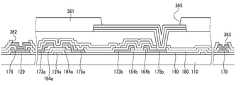
도 2는 본 발명의 한 실시예에 따른 유기 발광 표시 장치의 배치도이고, 도 3은 도 2의 유기 발광 표시 장치를 III-III 선을 따라 자른 단면도이다.FIG. 2 is a layout diagram of an organic light emitting display according to an embodiment of the present invention, and FIG. 3 is a cross-sectional view taken along a line III-III of the organic light emitting display of FIG.
투명한 유리 또는 플라스틱 따위로 만들어진 절연 기판(110) 위에 제1 제어 전극(control electrode)(124a)을 포함하는 복수의 게이트선(121)이 형성되어 있다.A plurality of
게이트선(121)은 게이트 신호를 전달하며 주로 가로 방향으로 뻗어 있다. 각 게이트선(121)은 다른 층 또는 외부 구동 회로와의 접속을 위하여 면적이 넓은 제1 패드부(129)을 포함하며, 제1 제어 전극(124a)은 게이트선(121)으로부터 위로 뻗어 있다.The
게이트선(121)은 알루미늄(Al)이나 알루미늄 합금 등 알루미늄 계열 금속, 은(Ag)이나 은 합금 등 은 계열 금속, 구리(Cu)나 구리 합금 등 구리 계열 금속, 몰리브덴(Mo)이나 몰리브덴 합금 등 몰리브덴 계열 금속, 크롬(Cr), 탄탈륨(Ta) 및 티타늄(Ti) 따위로 만들어질 수 있다. 그러나 이들은 물리적 성질이 다른 두 개의 도전막(도시하지 않음)을 포함하는 다중막 구조를 가질 수도 있다.The
게이트선(121)의 측면은 기판(110) 면에 대하여 경사져 있으며 그 경사각은 약 30° 내지 약 80° 인 것이 바람직하다.The side surface of the
게이트선(121) 위에는 질화규소(SiNx) 또는 산화규소(SiOx) 따위로 만들어진 하부 게이트 절연막(140)이 형성되어 있다.A lower gate
하부 게이트 절연막(140) 위에는 제1 반도체(154a)와 제2 반도체(154b)가 형성되어 있다. 제1 반도체(154a)와 제2 반도체(154b)는 미세 결정질 규소(microcrystalline silicon) 또는 다결정 규소(polycrystalline silicon)로 만들어진다.A
제1 반도체(154a)와 제2 반도체(154b) 위에는 각각 복수 쌍의 제1 저항성 접촉 부재(ohmic contact)(164a)와 복수 쌍의 제2 저항성 접촉 부재(164b)가 형성되어 있다. 저항성 접촉 부재(164a, 164b)는 섬 모양이며, 인(P) 따위의 n형 불순물이 고농도로 도핑되어 있는 n+ 수소화 비정질 규소 또는 미세 결정질 규소 따위의 물질로 만들어질 수 있다.A plurality of pairs of a first
저항성 접촉 부재(164a, 164b) 및 하부 게이트 절연막(140) 위에는 복수의 데이터선(171), 복수의 구동 전압선(172) 및 복수의 제1 및 제2 출력 전극(output electrode)(175a, 175b)을 포함하는 복수의 데이터 도전체(data conductor)가 형성되어 있다.A plurality of
데이터선(171)은 데이터 신호를 전달하며 주로 세로 방향으로 뻗어 게이트선(121)과 교차한다. 각 데이터선(171)은 제1 제어 전극(124a)을 향하여 뻗은 복수의 제1 입력 전극(input electrode)(173a)과 다른 층 또는 외부 구동 회로와의 접속을 위하여 면적이 넓은 제2 패드부(179)을 포함한다.The
구동 전압선(172)은 구동 전압을 전달하며 주로 세로 방향으로 뻗어 게이트선(121)과 교차한다. 각 구동 전압선(172)은 복수의 제2 입력 전극(173b)을 포함한다.The driving
제1 및 제2 출력 전극(175a, 175b)은 서로 분리되어 있고 데이터선(171) 및 구동 전압선(172)과도 분리되어 있다. 제1 입력 전극(173a)과 제1 출력 전극(175a)은 제1 반도체(154a)를 중심으로 서로 마주하고, 제2 입력 전극(173b)과 제2 출력 전극(175b)은 제2 반도체(154b)를 중심으로 서로 마주한다.The first and
데이터 도전체(171, 172, 175a, 175b)는 알루미늄, 구리 및 은 등 저저항 금속 또는 이들의 합금, 몰리브덴, 크롬, 탄탈륨 및 티타늄 등 내화성 금속 또는 이들의 합금으로 만들어지는 것이 바람직하며, 내화성 금속막(도시하지 않음)과 저저항 도전막(도시하지 않음)을 포함하는 다중막 구조를 가질 수 있다.The
게이트선(121)과 마찬가지로 데이터 도전체(171, 172, 175a, 175b) 또한 그 측면이 기판(110) 면에 대하여 30° 내지 80° 정도의 경사각으로 기울어진 것이 바람직하다.It is preferable that the
데이터 도전체(171, 172, 175a, 175b), 노출된 반도체(154a, 154b) 부분 및 하부 게이트 절연막(140) 위에는 질화규소 또는 산화규소 따위로 만들어진 상부 게이트 절연막(180)이 형성되어 있다.An upper
상부 게이트 절연막(180)에는 제1 출력 전극(175a), 제2 출력 전극(175b)을 드러내는 복수의 접촉 구멍(contact hole)(185a, 185b)이 형성되어 있다.A plurality of
상부 게이트 절연막(180) 위에는 제2 제어 전극(124b)이 형성되어 있다.And a
제2 제어 전극(124b)은 제2 반도체(154b)와 중첩하며, 유지 전극(storage electrode)(127)을 포함한다. 유지 전극(127)은 구동 전압선(172)과 중첩한다. 제2 제어 전극(124b)은 접촉 구멍(185a)을 통하여 제1 출력 전극(175a)과 연결되어 있다. The
제2 제어 전극(124b)은 게이트선(121)과 동일한 재료로 만들어질 수 있다.The
제2 제어 전극(124b)의 측면은 기판(110) 면에 대하여 경사져 있으며 그 경사각은 약 30° 내지 약 80° 인 것이 바람직하다.The side surface of the
제2 제어 전극(124b), 및 상부 게이트 절연막(180) 위에는 복수의 접촉 구멍(191, 192)을 갖는 복수의 보호 부재(193)가 형성되어 있다.A plurality of
이들은 산화 규소 또는 질화 규소 따위로 만들어질 수 있으며, 데이터 도전체(171, 172, 175a, 175b) 및 제2 패드부(179)를 보호하는 보호막(passivation layer)의 역할을 한다.These layers may be made of silicon oxide or silicon nitride, and serve as a passivation layer for protecting the
보호 부재(193)는 제2 제어 전극(124b)을 덮고 있다. 보호 부재(193)가 제2 제어 전극(124b) 위에 형성됨으로써, 내화학성이 약한 도전체로 만들어지는 제2 제어 전극(124b)이 후속 공정에서 식각액 따위의 화학액에 의해 손상되는 것을 방지할 수 있다.The
보호 부재(193) 위에는 접촉 구멍(201a)을 갖는 층간 절연막(201)이 형성되어 있다. 층간 절연막(201)은 스위칭 트랜지스터(Qs) 및 구동 트랜지스터(Qd)가 형성된 영역을 평탄화 할 수 있을 정도의 두께로 형성되며, 폴리이미드(Polyimide), 벤조사이클로부틴계 수지(benzocyclobutene series resin) 및 아크릴레이트(acrylate)로 이루어진 군에서 선택되는 1종의 물질로 형성될 수 있다.An interlayer insulating
층간 절연막(201) 및 보호 부재(193) 위에는 화소 전극(191) 및 복수의 접촉 보조 부재(81, 82)가 형성되어 있다.A
화소 전극(191) 및 복수의 접촉 보조 부재(81, 82)는 하부 화소 전극(191a), 반사 전극(191b) 및 상부 화소 전극(191c)으로 이루어진 3층 구조일 수 있다.The
이 때, 하부 화소 전극(191a)의 일부는 접촉 구멍(201a)을 통하여 제2 출력 전극(175)과 연결될 수 있으며, 접촉 구멍(201a) 내부에는 상기 하부 화소 전극(191a), 반사 전극(191b) 및 상부 화소 전극(191c) 각각의 일부를 포함할 수 있다.A portion of the
하부 화소 전극(191a)은 ITO(Indium Tin Oxide), IZO와 같은 투명한 금속 물질을 사용하여 50 ~ 200 Å 두께로 형성한다. 상기 하부 화소 전극(191a)은 후속 공정으로 형성되는 반사 전극(191b)과 보호 부재(193)간의 계면 특성, 즉 접착성을 향상시키기 위하여 형성된다.The
반사 전극(191b)은 반사도가 80%인 은(Ag), 팔라듐(Pd), 플라티늄(Pt) 등으로 형성할 수 있으며, 바람직하게는 은(Ag)을 이용하여 형성한다. 상기 반사 전극은 1000 ~ 3000 Å 두께로 형성한다. 이 때, 상기 반사 전극(191b)은 광 반사 역할을 하여 휘도와 광 효율을 증가시키는 역할을 할 수 있다.The
반사 전극(191b) 위에는 상부 화소 전극(191c)이 형성되어 있다. 상부 화소 전극(191c)은 ITO, IZO와 같은 투명한 금속 물질을 사용하여 50 ~ 200 Å 두께로 형성될 수 있다.An
접촉 보조 부재(81, 82)는 각각 접촉 구멍(191, 192)을 통하여 게이트선(121)의 제1 패드부(129) 및 데이터선(171)의 제2 패드부(179)과 연결된다. 접촉 보조 부재(81, 82)는 제1 패드부(129) 및 제2 패드부(179)와 외부 구동 회로와의 접착성을 보완하고 이들을 보호한다.The
화소 전극(191) 및 보호 부재(193) 위에는 격벽(partition)(361) 및 보호 격벽(362, 363)이 형성되어 있다. 격벽(361)은 화소 전극(191) 가장자리 주변을 둑(bank)처럼 둘러싸서 개구부(opening)(365)를 정의한다. 보호 격벽(362,363)은 접촉 보조 부재(81, 82) 가장자리 주변을 둘러싸고 있다. 이러한 보호 격벽(362, 363)은 접촉 보조 부재(81, 82)가 외부에 노출될 때 발생하는 부식 문제 및 황변 현상을 방지하는 역할을 한다.A
보호 격벽(362, 363)의 두께는 격벽(361)의 두께보다 두껍지 않게 형성하여, 접촉 보조 부재(81,82)와 외부 장치와의 접착성을 개선시킬 수 있다.The thicknesses of the
격벽(361) 및 보호 격벽(362, 363)은 아크릴 수지(acrylic resin), 폴리이미드 수지(polyimide resin) 따위의 내열성 및 내용매성을 가지는 유기 절연물 또는 산화규소(SiO2), 산화티탄(TiO2) 따위의 무기 절연물로 만들어질 수 있으며, 2층 이상일 수 있다. 격벽(361)은 또한 검정색 안료를 포함하는 감광재로 만들어질 수 있는데, 이 경우 격벽(361)은 차광 부재의 역할을 하며 그 형성 공정이 간단하다.
격벽(361)이 정의하는 화소 전극(191) 위의 개구부(365)에는 유기 발광 부 재(organic light emitting member)(370)가 형성되어 있다.An organic
유기 발광 부재(370)는 빛을 내는 발광층(emitting layer)(도시하지 않음) 외에 발광층의 발광 효율을 향상하기 위한 부대층(auxiliary layer)(도시하지 않음)을 포함하는 다층 구조를 가질 수 있다.The organic
발광층은 적색, 녹색, 청색의 삼원색 등 기본색(primary color) 중 어느 하나의 빛을 고유하게 내는 유기 물질 또는 유기 물질과 무기 물질의 혼합물로 만들어지며, 폴리플루오렌(polyfluorene) 유도체, (폴리)파라페닐렌비닐렌((poly)paraphenylenevinylene) 유도체, 폴리페닐렌(polyphenylene) 유도체, 폴리플루오렌(polyfluorene) 유도체, 폴리비닐카바졸(polyvinylcarbazole), 폴리티오펜(polythiophene) 유도체 또는 이들의 고분자 재료에 페릴렌(perylene)계 색소, 쿠마린(cumarine)계 색소, 로더민계 색소, 루브렌(rubrene), 페릴렌(perylene), 9,10-디페닐안트라센(9,10-diphenylanthracene), 테트라페닐부타디엔(tetraphenylbutadiene), 나일 레드(Nile red), 쿠마린(coumarin), 퀴나크리돈(quinacridone) 등을 도핑한 화합물이 포함될 수 있다. 유기 발광 표시 장치는 발광층에서 내는 기본색 색광의 공간적인 합으로 원하는 영상을 표시한다.The light emitting layer is made of a mixture of an organic material or an organic material and an inorganic material that uniquely emits light of any one of primary colors such as red, green, and blue, and includes a polyfluorene derivative, Polyphenylenevinylene derivatives, polyphenylene derivatives, polyfluorene derivatives, polyvinylcarbazole, polythiophene derivatives, and polymeric materials of these materials. Perylene pigments, cumarine pigments, rudder pigments, rubrene, perylene, 9,10-diphenylanthracene, tetraphenylbutadiene (hereinafter referred to as " tetraphenylbutadiene, Nile red, coumarin, quinacridone, and the like. The organic light emitting display displays a desired image with a spatial sum of basic color light emitted from the light emitting layer.
부대층에는 전자와 정공의 균형을 맞추기 위한 전자 수송층(electron transport layer)(도시하지 않음) 및 정공 수송층(hole transport layer)(도시하지 않음)과 전자와 정공의 주입을 강화하기 위한 전자 주입층(electron injecting layer)(도시하지 않음) 및 정공 주입층(hole injecting layer)(도시하지 않음) 등이 있으며, 이 중에서 선택된 하나 또는 둘 이상의 층을 포함할 수 있다. 정공 수 송층 및 정공 주입층은 화소 전극(191)과 발광층의 중간 정도의 일 함수를 가지는 재료로 만들어지고, 전자 수송층과 전자 주입층은 공통 전극(270)과 발광층의 중간 정도의 일 함수를 가지는 재료로 만들어진다. 예컨대 정공 수송층 또는 정공 주입층으로는 폴리에틸렌디옥시티오펜과 폴리스티렌술폰산의 혼합물(poly-(3,4-ethylenedioxythiophene: polystyrenesulfonate, PEDOT:PSS) 따위를 사용할 수 있다.The sub-layer includes an electron transport layer (not shown) and a hole transport layer (not shown) for balancing electrons and holes and an electron injection layer (not shown) for enhancing the injection of electrons and holes an electron injecting layer (not shown), and a hole injecting layer (not shown). The electron injecting layer may include one or two or more layers selected from the above. The hole transport layer and the hole injection layer are made of a material having a work function intermediate between the
유기 발광 부재(370) 위에는 공통 전극(common electrode)(270)이 형성되어 있다. 공통 전극(270)은 기판의 전면(全面)에 형성되어 있으며, 화소 전극(191)과 쌍을 이루어 유기 발광 부재(370)에 전류를 흘려 보낸다.A
이러한 유기 발광 표시 장치에서, 게이트선(121)에 연결되어 있는 제1 제어 전극(124a), 데이터선(171)에 연결되어 있는 제1 입력 전극(173a) 및 제1 출력 전극(175a)은 제1 반도체(154a)와 함께 스위칭 박막 트랜지스터(switching TFT)(Qs)를 이루며, 스위칭 박막 트랜지스터(Qs)의 채널(channel)은 제1 입력 전극(173a)과 제1 출력 전극(175a) 사이의 제1 반도체(154a)에 형성된다. 제1 출력 전극(175a)에 연결되어 있는 제2 제어 전극(124b), 구동 전압선(172)에 연결되어 있는 제2 입력 전극(173b) 및 화소 전극(191)에 연결되어 있는 제2 출력 전극(175b)은 제2 반도체(154b)와 함께 구동 박막 트랜지스터(driving TFT)(Qd)를 이루며, 구동 박막 트랜지스터(Qd)의 채널은 제2 입력 전극(173b)과 제2 출력 전극(175b) 사이의 제2 반도체(154b)에 형성된다.The
본 실시예에서는 스위칭 박막 트랜지스터 1개와 구동 박막 트랜지스터 1개만 을 도시하였지만 이들 외에 적어도 하나의 박막 트랜지스터 및 이를 구동하기 위한 복수의 배선을 더 포함함으로써, 장시간 구동하여도 유기 발광 다이오드(LD) 및 구동 트랜지스터(Qd)가 열화되는 것을 방지하거나 보상하여 유기 발광 표시 장치의 수명이 단축되는 것을 방지할 수 있다.In this embodiment, only one switching thin film transistor and one driving thin film transistor are shown, but in addition to these, at least one thin film transistor and a plurality of wirings for driving the thin film transistor are further included, so that even if driven for a long time, It is possible to prevent or compensate for degradation of the organic light emitting diode Qd and shorten the lifetime of the OLED display.
화소 전극(191), 유기 발광 부재(370) 및 공통 전극(270)은 유기 발광 다이오드(LD)를 이루며, 화소 전극(191)이 애노드(anode), 공통 전극(270)이 캐소드(cathode)가 되거나 반대로 화소 전극(191)이 캐소드, 공통 전극(270)이 애노드가 된다. 또한 서로 중첩하는 유지 전극(127)과 구동 전압선(172)은 유지 축전기(storage capacitor)(Cst)를 이룬다.The
그러면 도 2 및 도 3에 도시한 유기 발광 표시 장치를 제조하는 방법에 대하여 도 4 내지 도 9를 참조하여 상세하게 설명한다.2 and 3 will be described in detail with reference to FIGS. 4 to 9. FIG.
도 4 내지 도9는 도 2 및 도 3의 유기 발광 표시 장치를 본 발명의 한 실시예에 따라 제조하는 방법의 중간 단계에서의 단면도이다.FIGS. 4 to 9 are cross-sectional views at intermediate stages of the method of manufacturing the organic light emitting display of FIGS. 2 and 3 according to one embodiment of the present invention.
도 4 에 도시한 바와 같이, 기판(110) 위에 알루미늄 합금으로 만들어진 제1 제어 전극(124a) 및 패드부(129)를 포함하는 복수의 게이트선(121)을 형성한다.A plurality of
다음, 게이트 절연층을 화학 기상 증착 방법(plasma enhanced chemical vapor deposition, PECVD)으로 증착한 후, 사진 식각하여 복수의 게이트선의 패드부(129)을 노출하는 하부 게이트 절연막(140)을 형성한다.Next, the gate insulating layer is deposited by plasma enhanced chemical vapor deposition (PECVD), and then the bottom
다음, 진성 비정질 규소층, 및 불순물 비정질 규소층을 화학 기상 증착 방법(PECVD)으로 연속하여 적층한다.Next, the intrinsic amorphous silicon layer and the impurity amorphous silicon layer are successively laminated by chemical vapor deposition (PECVD).
다음, 불순물 비정질 규소층 및 진성 비정질 규소층을 사진 식각하여 복수의 제1 및 제2 저항성 접촉 부재(164a, 164b), 복수의 제1 및 제2 반도체(154a, 154b)를 형성한다. 이 때, 상기 복수의 제1 및 제2 저항성 접촉 부재(164a, 164b), 복수의 제1 및 제2 반도체(154a, 154b)를 ELA(Excimer Laser Annealing), SLS(Sequential Lateral Solidification) 또는 SPC(Solid Phase Crystallization)와 같은 결정화 방법 등을 사용하여 결정화할 수 있다.Next, the impurity amorphous silicon layer and the intrinsic amorphous silicon layer are photo-etched to form a plurality of first and second
다음, 알루미늄 합금으로 만들어진 제1 입력 전극(173a)과 제2 패드부(179)를 포함하는 복수의 데이터선(171), 제2 입력 전극(173b)을 포함하는 구동 전압선(172) 및 복수의 제1 및 제2 출력 전극(175a, 175b)을 포함하는 데이터 도전체를 형성한다. 이 때, 제1 패드부(129) 위에 데이터 도전체와 동일한 물질로 패드부 보조 부재(178)가 형성될 수 있다. 패드부 보조 부재(178)는 제1 패드부(129)와 향후에 형성되는 접촉 보조 부재(81)를 전기적으로 연결해주는 역할을 한다.Next, a plurality of
다음, 도 5에 도시한 바와 같이, 기판 전면에 화학 기상 증착 방법으로 상부 게이트 절연층을 적층하고 사진 식각하여 복수의 접촉 구멍(185a, 185b)을 갖는 상부 게이트 절연막(180)을 형성한다.Next, as shown in FIG. 5, an upper gate insulating layer is deposited on the entire surface of the substrate by a chemical vapor deposition method, and is photo-etched to form a top
다음, 도 6에 도시한 바와 같이, 알루미늄 합금으로 만들어진 도전층을 적층하고 사진 식각하여 유지 전극(127)을 포함하는 제2 제어 전극(124b)을 형성한다.Next, as shown in FIG. 6, a conductive layer made of an aluminum alloy is laminated and photolithographically etched to form a
다음, 도 7에 도시한 바와 같이, 상부 게이트 절연막(180) 및 제2 제어 전극(124b) 위에 복수의 접촉 구멍(191, 192, 194)를 갖는 보호부재(193)를 사진 식각하여 형성한다.7, a
다음, 도 8에 도시한 바와 같이, 보호 부재(193) 위에 복수의 접촉 구멍(201a)를 갖는 층간 절연막(201)을 형성한다.Next, as shown in Fig. 8, an
다음, 도 9에 도시한 바와 같이, 층간 절연막(201) 및 제2 패드부(179) 위에 ITO, Ag, ITO를 연속적으로 증착한 후, 사진 식각하여 복수의 화소 전극(191) 및 복수의 접촉 보조 부재(81, 82)를 형성한다.9, ITO, Ag, and ITO are successively deposited on the
다음, 도 10에 도시한 바와 같이, 복수의 화소 전극(191), 층간 절연막(201) 및 복수의 접촉 보조 부재(81,82) 위에 감광성 유기막을 도포한 후 노광 및 현상하여 복수의 개구부(365)를 가지는 격벽(361)과 복수의 보호 격벽(362, 363)을 형성한다. 이 때, 슬릿 마스크(Slit Mask)를 사용하여 격벽(361)보다 단차가 낮은 복수의 보호 격벽(362, 363)을 형성할 수 있다.10, a photosensitive organic film is coated on the plurality of
다음, 도 3에 도시한 바와 같이, 개구부(365)에 정공 수송층(도시하지 않음) 및 발광층(도시하지 않음)을 포함한 발광 부재(370)를 형성한다. 발광 부재(370)는 잉크젯 인쇄(inkjet printing) 방법 등의 용액 방법(solution process) 또는 증착 방법으로 형성할 수 있으며, 그 중 잉크젯 헤드(inkjet head)(도시하지 않음)를 이동시키며 개구부(365)에 용액을 적하하는 잉크젯 인쇄방법을 이용할 경우, 각 층의 형성 후 건조 단계가 뒤따른다.Next, as shown in Fig. 3, a
이어서, 격벽(361) 및 발광 부재(370) 위에 공통 전극(270)을 형성한다.Next, a
이와 같이, 본 실시예에서는 스위칭 박막 트랜지스터는 바텀 게이트(bottom gate) 구조로 형성하고 구동 박막 트랜지스터는 탑 게이트(top gate) 구조로 형성한다.Thus, in this embodiment, the switching thin film transistor is formed as a bottom gate structure and the driving thin film transistor is formed as a top gate structure.
그러나 이에 한정되지 않고 스위칭 박막 트랜지스터를 탑 게이트 구조로 형성하고 구동 박막 트랜지스터를 바텀 게이트 구조로 형성할 수도 있다.However, the present invention is not limited thereto, and the switching thin film transistor may be formed as a top gate structure and the driving thin film transistor may be formed as a bottom gate structure.
어느 경우든, 스위칭 박막 트랜지스터와 구동 박막 트랜지스터가 다른 구조로 형성되는 경우에도 공통되는 층을 통합하여 마스크 수를 줄임으로써 공정을 단순화할 수 있다.In any case, even when the switching thin film transistor and the driving thin film transistor are formed in different structures, the number of masks can be reduced by integrating common layers, thereby simplifying the process.
또한, 본 실시예에서는 발광 부재(370)의 빛이 공통 전극(270)이 형성된 방향으로 발광되는 탑 이미션(Top-Emission)구조로 형성하였으나, 그러나 이에 한정되지 않고 공통 전극(270)과 화소 전극(191)의 위치를 바꾸어, 바텀 이미션(Bottom-Emission)구조로 형성하여 발광 부재(370)의 빛이 탑 이미션(Top-Emission)과 반대방향으로 발광되도록 할 수 있다.In this embodiment, the
이상에서 본 발명의 바람직한 실시예들에 대하여 상세하게 설명하였지만 본 발명의 권리 범위는 이에 한정되는 것은 아니고 다음의 청구 범위에서 정의하고 있는 본 발명의 기본 개념을 이용한 당업자의 여러 변형 및 개량 형태 또한 본 발명의 권리 범위에 속하는 것이다.While the present invention has been particularly shown and described with reference to exemplary embodiments thereof, it is to be understood that the invention is not limited to the disclosed exemplary embodiments, And falls within the scope of the invention.
도 1은 본 발명의 한 실시예에 따른 유기 발광 표시 장치의 등가 회로도이고,1 is an equivalent circuit diagram of an OLED display according to an embodiment of the present invention,
도 2는 본 발명의 한 실시예에 따른 유기 발광 표시 장치의 배치도이고,2 is a layout diagram of an OLED display according to an embodiment of the present invention,
도 3은 도 2의 유기 발광 표시 장치를 III-III 선을 따라 자른 단면도이고,FIG. 3 is a cross-sectional view of the organic light emitting diode display of FIG. 2 taken along line III-III,
도 4 내지 도 10은 도 2 및 도 3에서의 유기 발광 표시 장치를 본 발명의 한 실시예에 따라 제조하는 방법의 중간 단계에서의 단면도이다.Figs. 4 to 10 are cross-sectional views at intermediate stages of a method of manufacturing the organic light emitting display device of Figs. 2 and 3 according to an embodiment of the present invention.
<도면의 주요 부분에 대한 부호 설명>Description of the Related Art [0002]
110 : 절연기판121 : 게이트선110: Insulation substrate 121: Gate line
171 : 데이터선172 : 구동 전압선171: Data line 172: Driving voltage line
129 : 제1 패드부179 : 제2 패드부129: first pad portion 179: second pad portion
81, 82 : 접촉 보조 부재362,363 : 보호 격벽81, 82:
191 : 화소 전극361 : 격벽191: pixel electrode 361: partition wall
Claims (15)
Translated fromKoreanPriority Applications (4)
| Application Number | Priority Date | Filing Date | Title |
|---|---|---|---|
| KR1020080059042AKR101499235B1 (en) | 2008-06-23 | 2008-06-23 | Organic light emitting display and manufacturing method thereof |
| US12/343,266US7948173B2 (en) | 2008-06-23 | 2008-12-23 | Organic light emitting diode display and method of manufacturing the same |
| CN200910002540.2ACN101615626B (en) | 2008-06-23 | 2009-01-16 | Organic light emitting diode display and method of manufacturing the same |
| JP2009025314AJP5302033B2 (en) | 2008-06-23 | 2009-02-05 | Organic light-emitting display device and method for manufacturing the same |
Applications Claiming Priority (1)
| Application Number | Priority Date | Filing Date | Title |
|---|---|---|---|
| KR1020080059042AKR101499235B1 (en) | 2008-06-23 | 2008-06-23 | Organic light emitting display and manufacturing method thereof |
Publications (2)
| Publication Number | Publication Date |
|---|---|
| KR20090132860A KR20090132860A (en) | 2009-12-31 |
| KR101499235B1true KR101499235B1 (en) | 2015-03-06 |
Family
ID=41430513
Family Applications (1)
| Application Number | Title | Priority Date | Filing Date |
|---|---|---|---|
| KR1020080059042AActiveKR101499235B1 (en) | 2008-06-23 | 2008-06-23 | Organic light emitting display and manufacturing method thereof |
Country Status (4)
| Country | Link |
|---|---|
| US (1) | US7948173B2 (en) |
| JP (1) | JP5302033B2 (en) |
| KR (1) | KR101499235B1 (en) |
| CN (1) | CN101615626B (en) |
Cited By (5)
| Publication number | Priority date | Publication date | Assignee | Title |
|---|---|---|---|---|
| KR20160141176A (en)* | 2015-05-28 | 2016-12-08 | 엘지디스플레이 주식회사 | Organic light emitting display device and method of manufacturing the same |
| KR20180003302A (en)* | 2016-06-30 | 2018-01-09 | 엘지디스플레이 주식회사 | Backplane Substrate, Manufacturing Method for the Same, and Organic Light Emitting Display Device Using the Same |
| US10692954B2 (en) | 2016-11-22 | 2020-06-23 | Samsung Display Co., Ltd. | Backplane for display device and method of manufacturing the same |
| KR20200107012A (en)* | 2019-03-05 | 2020-09-16 | 삼성디스플레이 주식회사 | Display device and manufacturing method of the same |
| KR20220150233A (en)* | 2014-07-23 | 2022-11-10 | 엘지디스플레이 주식회사 | Organic light emitting diode display device and fabricating method of the same |
Families Citing this family (55)
| Publication number | Priority date | Publication date | Assignee | Title |
|---|---|---|---|---|
| KR101592013B1 (en)* | 2008-10-13 | 2016-02-05 | 삼성디스플레이 주식회사 | Organic light emitting diode display and method for manufacturing the same |
| CN102498570B (en) | 2009-09-04 | 2016-02-10 | 株式会社半导体能源研究所 | Light emitting device and manufacturing method thereof |
| WO2011027676A1 (en) | 2009-09-04 | 2011-03-10 | Semiconductor Energy Laboratory Co., Ltd. | Semiconductor device and manufacturing method thereof |
| JP2012019118A (en)* | 2010-07-09 | 2012-01-26 | Casio Comput Co Ltd | Transistor structure, method for manufacturing transistor structure, and light-emitting device |
| KR20120005793A (en)* | 2010-07-09 | 2012-01-17 | 삼성모바일디스플레이주식회사 | Display device |
| JP2012064604A (en)* | 2010-09-14 | 2012-03-29 | Casio Comput Co Ltd | Transistor structure, method of manufacturing transistor structure, and light-emitting device |
| TWI459563B (en)* | 2011-04-01 | 2014-11-01 | Chunghwa Picture Tubes Ltd | Transistor array substrate |
| KR101945237B1 (en) | 2012-06-01 | 2019-02-08 | 삼성디스플레이 주식회사 | Organic light emitting diode display |
| KR102022396B1 (en)* | 2013-02-20 | 2019-09-19 | 삼성디스플레이 주식회사 | Organic light emitting display device and method of manufacturing thereof |
| CN103077957B (en)* | 2013-02-22 | 2015-09-02 | 深圳市华星光电技术有限公司 | Active matrix organic LED display device and preparation method thereof |
| KR102143924B1 (en)* | 2013-07-12 | 2020-08-13 | 삼성디스플레이 주식회사 | Organic light emitting diode display |
| KR102100372B1 (en)* | 2013-08-28 | 2020-04-14 | 삼성디스플레이 주식회사 | Organic light-emitting display apparatus |
| KR102131963B1 (en)* | 2013-10-15 | 2020-07-09 | 삼성디스플레이 주식회사 | Organic light-emitting display apparatus |
| KR102322700B1 (en)* | 2014-05-23 | 2021-11-04 | 엘지디스플레이 주식회사 | Organic light emitting diode display device and the emthod fof fabricating the same |
| US9806279B2 (en)* | 2014-07-08 | 2017-10-31 | Lg Display Co., Ltd. | Organic light emitting display device comprising auxiliary electrode having void therein and manufacturing method thereof |
| KR102653947B1 (en)* | 2014-07-11 | 2024-04-03 | 엘지디스플레이 주식회사 | Display device and method of fabricating the same |
| US10181573B2 (en)* | 2014-07-11 | 2019-01-15 | Lg Display Co., Ltd. | Organic light-emitting diode display device and method of fabricating the same |
| KR102361967B1 (en)* | 2014-07-11 | 2022-02-11 | 엘지디스플레이 주식회사 | Organic light emitting diode display device |
| KR102230575B1 (en)* | 2014-08-05 | 2021-03-19 | 엘지디스플레이 주식회사 | Organic light emitting display device and method of manufacturing the same |
| KR102373082B1 (en)* | 2014-07-16 | 2022-03-10 | 엘지디스플레이 주식회사 | Organic light emitting display device and method of manufacturing the same |
| KR102230692B1 (en)* | 2014-07-29 | 2021-03-19 | 엘지디스플레이 주식회사 | Organic light emitting display device and method of manufacturing the same |
| KR102320186B1 (en)* | 2014-07-18 | 2021-10-29 | 엘지디스플레이 주식회사 | Organic light emitting display device and method of fabricating the same |
| CN110246850B (en) | 2014-07-23 | 2022-12-02 | 索尼公司 | Display device |
| KR102301837B1 (en)* | 2014-09-12 | 2021-09-14 | 엘지디스플레이 주식회사 | Organic Light Emitting Display Device and Method for Manufacturing The Same |
| KR102225253B1 (en)* | 2014-09-15 | 2021-03-09 | 엘지디스플레이 주식회사 | Organic Light Emitting Display Device and Method for Manufacturing The Same |
| KR102220787B1 (en)* | 2014-09-17 | 2021-02-26 | 엘지디스플레이 주식회사 | Organic Light Emitting Display Device and Method for Manufacturing The Same |
| KR102283025B1 (en)* | 2014-10-20 | 2021-07-27 | 엘지디스플레이 주식회사 | Organic light emitting display device and method of manufacturing the same |
| KR102349285B1 (en)* | 2014-11-17 | 2022-01-11 | 삼성디스플레이 주식회사 | Organic light-emitting display apparatus and manufacturing method of the same |
| KR102374713B1 (en)* | 2014-12-18 | 2022-03-15 | 엘지디스플레이 주식회사 | Display panel and organic electroluminescent display appartus having the same |
| KR20160075194A (en) | 2014-12-19 | 2016-06-29 | 백윤근 | Arcuate cutting device for wood |
| KR102453043B1 (en)* | 2014-12-19 | 2022-10-11 | 엘지디스플레이 주식회사 | Organic light emitting display device and method of manufacturing the same |
| KR102377531B1 (en)* | 2015-01-23 | 2022-03-22 | 삼성디스플레이 주식회사 | Organic light emitting display device and manufacturing method thereof |
| KR102482208B1 (en)* | 2015-01-28 | 2022-12-28 | 엘지디스플레이 주식회사 | Organic light emitting diodes improving display quality |
| KR102369300B1 (en)* | 2015-02-24 | 2022-03-03 | 삼성디스플레이 주식회사 | Organic light emitting display device and manufacturing method of the same |
| KR102540372B1 (en)* | 2015-05-28 | 2023-06-05 | 엘지디스플레이 주식회사 | Organic light emitting display device and method of manufacturing the same |
| KR102545253B1 (en)* | 2015-05-28 | 2023-06-19 | 엘지디스플레이 주식회사 | Organic light emitting display device and method of manufacturing the same |
| KR102515033B1 (en)* | 2015-05-29 | 2023-03-28 | 엘지디스플레이 주식회사 | Organic light emitting display device and method of manufacturing the same |
| KR102520874B1 (en)* | 2015-05-29 | 2023-04-12 | 엘지디스플레이 주식회사 | Organic light emitting display device and method of manufacturing the same |
| KR101879180B1 (en)* | 2015-11-16 | 2018-07-17 | 엘지디스플레이 주식회사 | Organic light emitting display device and method of manufacturing the same |
| KR102665790B1 (en)* | 2016-01-14 | 2024-05-14 | 삼성디스플레이 주식회사 | Display panel and method of manufacturing the same |
| JP6685142B2 (en)* | 2016-02-02 | 2020-04-22 | 株式会社ジャパンディスプレイ | Display device and manufacturing method thereof |
| KR102637068B1 (en)* | 2016-06-01 | 2024-02-16 | 삼성디스플레이 주식회사 | Display apparatus and fabricating method of the same |
| KR102491880B1 (en)* | 2016-06-16 | 2023-01-27 | 삼성디스플레이 주식회사 | Organic light emitting display and manufacturing method thereof |
| KR102656232B1 (en)* | 2016-08-31 | 2024-04-09 | 엘지디스플레이 주식회사 | Organic Light Emitting Array and Organic Light Emitting Display Device Using the Same |
| KR102556961B1 (en)* | 2016-12-21 | 2023-07-20 | 엘지디스플레이 주식회사 | Photo Mask and Display Panel using thereof and Method for Fabricating Display Panel using the thereof |
| KR102682193B1 (en)* | 2016-12-28 | 2024-07-04 | 엘지디스플레이 주식회사 | Array substrate and Display device including the same |
| KR102515814B1 (en)* | 2017-05-25 | 2023-03-31 | 삼성디스플레이 주식회사 | Display device |
| KR102470375B1 (en)* | 2017-10-31 | 2022-11-23 | 엘지디스플레이 주식회사 | Display apparatus |
| KR102768947B1 (en)* | 2018-11-28 | 2025-02-18 | 삼성전자주식회사 | An electronic device including an display panel formed of electrodes of different shapes for each region |
| KR20220006541A (en) | 2019-05-10 | 2022-01-17 | 가부시키가이샤 한도오따이 에네루기 켄큐쇼 | Display devices and electronic devices |
| KR20210022206A (en)* | 2019-08-19 | 2021-03-03 | 삼성디스플레이 주식회사 | Organic light emitting diode display device and manufacturing method thereof |
| US12010886B2 (en)* | 2020-01-22 | 2024-06-11 | Chengdu Boe Optoelectronics Technology Co., Ltd. | Display panel and display device |
| CN112242498A (en)* | 2020-10-20 | 2021-01-19 | 安徽熙泰智能科技有限公司 | Silicon-based OLED micro-display craft product and preparation method thereof |
| KR20220060021A (en)* | 2020-11-02 | 2022-05-11 | 삼성디스플레이 주식회사 | Display apparatus |
| KR102864432B1 (en)* | 2021-07-14 | 2025-09-25 | 삼성디스플레이 주식회사 | Display device |
Citations (3)
| Publication number | Priority date | Publication date | Assignee | Title |
|---|---|---|---|---|
| US20050110023A1 (en)* | 2003-11-24 | 2005-05-26 | Kwan-Hee Lee | Organic light-emitting display |
| JP2005183209A (en)* | 2003-12-19 | 2005-07-07 | Asahi Glass Co Ltd | Organic EL display device and manufacturing method thereof |
| JP2007140530A (en)* | 2005-11-17 | 2007-06-07 | Samsung Electronics Co Ltd | Organic light emitting display |
Family Cites Families (18)
| Publication number | Priority date | Publication date | Assignee | Title |
|---|---|---|---|---|
| KR100490043B1 (en) | 1998-01-21 | 2005-08-31 | 삼성전자주식회사 | Planar drive type liquid crystal display device and its manufacturing method |
| JP2002270372A (en) | 2001-03-14 | 2002-09-20 | Toshiba Corp | Manufacturing method of organic EL display device |
| KR100477746B1 (en)* | 2002-06-22 | 2005-03-18 | 삼성에스디아이 주식회사 | Organic electroluminescence device employing multi-layered anode |
| JP2004165068A (en) | 2002-11-14 | 2004-06-10 | Sanyo Electric Co Ltd | Method for manufacturing organic electroluminescent panel |
| KR101087567B1 (en) | 2004-03-23 | 2011-11-28 | 엘지디스플레이 주식회사 | Organic electroluminescent device and manufacturing method thereof |
| KR100653265B1 (en)* | 2004-04-19 | 2006-12-06 | 엘지.필립스 엘시디 주식회사 | Dual panel type organic electroluminescent device and manufacturing method thereof |
| KR100712108B1 (en) | 2004-12-10 | 2007-04-27 | 삼성에스디아이 주식회사 | Organic electroluminescent display and manufacturing method thereof |
| KR101122231B1 (en)* | 2004-12-17 | 2012-03-19 | 삼성전자주식회사 | Thin film transistor array panel using organic semiconductor and manufacturing method thereof |
| JP2006251281A (en) | 2005-03-10 | 2006-09-21 | Seiko Epson Corp | ELECTRO-OPTICAL DEVICE, MANUFACTURING METHOD THEREOF, IMAGE FORMING DEVICE, AND IMAGE READING DEVICE |
| KR100731739B1 (en) | 2005-04-28 | 2007-06-22 | 삼성에스디아이 주식회사 | Organic electroluminescent device and manufacturing method thereof |
| KR100711889B1 (en) | 2005-07-18 | 2007-04-25 | 삼성에스디아이 주식회사 | OLED display device and manufacturing method thereof |
| KR100730151B1 (en) | 2005-09-30 | 2007-06-19 | 삼성에스디아이 주식회사 | Flat panel display |
| US8017950B2 (en)* | 2005-12-29 | 2011-09-13 | Lg Display Co., Ltd. | Organic electro-luminescence display device and method of manfacturing the same |
| JP4809087B2 (en) | 2006-03-14 | 2011-11-02 | セイコーエプソン株式会社 | ELECTROLUMINESCENT DEVICE, ELECTRONIC DEVICE, AND METHOD FOR MANUFACTURING ELECTROLUMINESCENT DEVICE |
| KR100759680B1 (en) | 2006-06-09 | 2007-09-17 | 삼성에스디아이 주식회사 | Mask and manufacturing method of organic electroluminescent display using same |
| KR101293562B1 (en)* | 2006-06-21 | 2013-08-06 | 삼성디스플레이 주식회사 | Organic light emitting diode display and method for manufacturing the same |
| JP4872510B2 (en)* | 2006-08-01 | 2012-02-08 | カシオ計算機株式会社 | Display panel using light emitting element and method for manufacturing the same |
| JP5028900B2 (en)* | 2006-08-01 | 2012-09-19 | カシオ計算機株式会社 | Display panel manufacturing method using light emitting element |
- 2008
- 2008-06-23KRKR1020080059042Apatent/KR101499235B1/enactiveActive
- 2008-12-23USUS12/343,266patent/US7948173B2/enactiveActive
- 2009
- 2009-01-16CNCN200910002540.2Apatent/CN101615626B/enactiveActive
- 2009-02-05JPJP2009025314Apatent/JP5302033B2/ennot_activeExpired - Fee Related
Patent Citations (3)
| Publication number | Priority date | Publication date | Assignee | Title |
|---|---|---|---|---|
| US20050110023A1 (en)* | 2003-11-24 | 2005-05-26 | Kwan-Hee Lee | Organic light-emitting display |
| JP2005183209A (en)* | 2003-12-19 | 2005-07-07 | Asahi Glass Co Ltd | Organic EL display device and manufacturing method thereof |
| JP2007140530A (en)* | 2005-11-17 | 2007-06-07 | Samsung Electronics Co Ltd | Organic light emitting display |
Cited By (10)
| Publication number | Priority date | Publication date | Assignee | Title |
|---|---|---|---|---|
| KR20220150233A (en)* | 2014-07-23 | 2022-11-10 | 엘지디스플레이 주식회사 | Organic light emitting diode display device and fabricating method of the same |
| KR102650509B1 (en) | 2014-07-23 | 2024-03-22 | 엘지디스플레이 주식회사 | Organic light emitting diode display device and fabricating method of the same |
| KR20160141176A (en)* | 2015-05-28 | 2016-12-08 | 엘지디스플레이 주식회사 | Organic light emitting display device and method of manufacturing the same |
| KR102452198B1 (en)* | 2015-05-28 | 2022-10-07 | 엘지디스플레이 주식회사 | Organic light emitting display device and method of manufacturing the same |
| KR20180003302A (en)* | 2016-06-30 | 2018-01-09 | 엘지디스플레이 주식회사 | Backplane Substrate, Manufacturing Method for the Same, and Organic Light Emitting Display Device Using the Same |
| KR102675912B1 (en)* | 2016-06-30 | 2024-06-17 | 엘지디스플레이 주식회사 | Backplane Substrate, Manufacturing Method for the Same, and Organic Light Emitting Display Device Using the Same |
| US10692954B2 (en) | 2016-11-22 | 2020-06-23 | Samsung Display Co., Ltd. | Backplane for display device and method of manufacturing the same |
| US11164932B2 (en) | 2016-11-22 | 2021-11-02 | Samsung Display Co., Ltd. | Backplane for display device and method of manufacturing the same |
| KR20200107012A (en)* | 2019-03-05 | 2020-09-16 | 삼성디스플레이 주식회사 | Display device and manufacturing method of the same |
| KR102854478B1 (en) | 2019-03-05 | 2025-09-03 | 삼성디스플레이 주식회사 | Display device and manufacturing method of the same |
Also Published As
| Publication number | Publication date |
|---|---|
| JP2010003668A (en) | 2010-01-07 |
| US7948173B2 (en) | 2011-05-24 |
| US20090315451A1 (en) | 2009-12-24 |
| KR20090132860A (en) | 2009-12-31 |
| JP5302033B2 (en) | 2013-10-02 |
| CN101615626B (en) | 2014-12-17 |
| CN101615626A (en) | 2009-12-30 |
Similar Documents
| Publication | Publication Date | Title |
|---|---|---|
| KR101499235B1 (en) | Organic light emitting display and manufacturing method thereof | |
| US7863602B2 (en) | Organic light emitting diode display and method for manufacturing the same | |
| KR101293562B1 (en) | Organic light emitting diode display and method for manufacturing the same | |
| US7710019B2 (en) | Organic light-emitting diode display comprising auxiliary electrodes | |
| KR101294260B1 (en) | Organic light emitting diode display and method for manufacturing the same | |
| US7883921B2 (en) | Thin film transistor array panel and manufacturing method thereof | |
| US7564060B2 (en) | Display device preventing short of driving voltage lines | |
| US20070188089A1 (en) | Organic light emitting device and manufacturing method of the same | |
| KR100700644B1 (en) | Organic Electroluminescence Display Device Having the Second Electrode Power Resources Suppling Line and Fabricating of the same | |
| KR20100023559A (en) | Organic light emitting diode display and method for manufacturing the same | |
| US20080150417A1 (en) | Organic light emitting display device and method of manufacturing the same | |
| KR101240648B1 (en) | Organic light emitting diode display and method for manufacturing the same | |
| KR101240649B1 (en) | Organic light emitting diode display and method for manufacturing the same | |
| KR101534009B1 (en) | Thin film transistor display panel, method of manufacturing the same, and display device having thin film transistor panel | |
| KR101189276B1 (en) | Organic light emitting diode display and method for manufacturing thereof | |
| KR101367130B1 (en) | Organic light emitting diode display | |
| KR101143006B1 (en) | Organic light emitting diode display and method for manufacturing thereof | |
| KR20080006894A (en) | Display device and manufacturing method thereof | |
| KR20080050690A (en) | Manufacturing Method of Organic Light Emitting Display | |
| KR20080055247A (en) | Manufacturing Method of Organic Light Emitting Display |
Legal Events
| Date | Code | Title | Description |
|---|---|---|---|
| PA0109 | Patent application | Patent event code:PA01091R01D Comment text:Patent Application Patent event date:20080623 | |
| PG1501 | Laying open of application | ||
| N231 | Notification of change of applicant | ||
| PN2301 | Change of applicant | Patent event date:20120913 Comment text:Notification of Change of Applicant Patent event code:PN23011R01D | |
| A201 | Request for examination | ||
| PA0201 | Request for examination | Patent event code:PA02012R01D Patent event date:20130417 Comment text:Request for Examination of Application Patent event code:PA02011R01I Patent event date:20080623 Comment text:Patent Application | |
| E902 | Notification of reason for refusal | ||
| PE0902 | Notice of grounds for rejection | Comment text:Notification of reason for refusal Patent event date:20140723 Patent event code:PE09021S01D | |
| E701 | Decision to grant or registration of patent right | ||
| PE0701 | Decision of registration | Patent event code:PE07011S01D Comment text:Decision to Grant Registration Patent event date:20141223 | |
| GRNT | Written decision to grant | ||
| PR0701 | Registration of establishment | Comment text:Registration of Establishment Patent event date:20150227 Patent event code:PR07011E01D | |
| PR1002 | Payment of registration fee | Payment date:20150227 End annual number:3 Start annual number:1 | |
| PG1601 | Publication of registration | ||
| FPAY | Annual fee payment | Payment date:20180201 Year of fee payment:4 | |
| PR1001 | Payment of annual fee | Payment date:20180201 Start annual number:4 End annual number:4 | |
| FPAY | Annual fee payment | Payment date:20190129 Year of fee payment:5 | |
| PR1001 | Payment of annual fee | Payment date:20190129 Start annual number:5 End annual number:5 | |
| FPAY | Annual fee payment | Payment date:20200203 Year of fee payment:6 | |
| PR1001 | Payment of annual fee | Payment date:20200203 Start annual number:6 End annual number:6 | |
| PR1001 | Payment of annual fee | Payment date:20210201 Start annual number:7 End annual number:7 | |
| PR1001 | Payment of annual fee | Payment date:20220127 Start annual number:8 End annual number:8 |