KR101497651B1 - Display device and driving method thereof - Google Patents
Display device and driving method thereofDownload PDFInfo
- Publication number
- KR101497651B1 KR101497651B1KR1020080086963AKR20080086963AKR101497651B1KR 101497651 B1KR101497651 B1KR 101497651B1KR 1020080086963 AKR1020080086963 AKR 1020080086963AKR 20080086963 AKR20080086963 AKR 20080086963AKR 101497651 B1KR101497651 B1KR 101497651B1
- Authority
- KR
- South Korea
- Prior art keywords
- frequency
- dimming
- signal
- frequencies
- frame
- Prior art date
- Legal status (The legal status is an assumption and is not a legal conclusion. Google has not performed a legal analysis and makes no representation as to the accuracy of the status listed.)
- Expired - Fee Related
Links
Images


Classifications
- G—PHYSICS
- G09—EDUCATION; CRYPTOGRAPHY; DISPLAY; ADVERTISING; SEALS
- G09G—ARRANGEMENTS OR CIRCUITS FOR CONTROL OF INDICATING DEVICES USING STATIC MEANS TO PRESENT VARIABLE INFORMATION
- G09G3/00—Control arrangements or circuits, of interest only in connection with visual indicators other than cathode-ray tubes
- G09G3/20—Control arrangements or circuits, of interest only in connection with visual indicators other than cathode-ray tubes for presentation of an assembly of a number of characters, e.g. a page, by composing the assembly by combination of individual elements arranged in a matrix no fixed position being assigned to or needed to be assigned to the individual characters or partial characters
- G09G3/34—Control arrangements or circuits, of interest only in connection with visual indicators other than cathode-ray tubes for presentation of an assembly of a number of characters, e.g. a page, by composing the assembly by combination of individual elements arranged in a matrix no fixed position being assigned to or needed to be assigned to the individual characters or partial characters by control of light from an independent source
- G09G3/36—Control arrangements or circuits, of interest only in connection with visual indicators other than cathode-ray tubes for presentation of an assembly of a number of characters, e.g. a page, by composing the assembly by combination of individual elements arranged in a matrix no fixed position being assigned to or needed to be assigned to the individual characters or partial characters by control of light from an independent source using liquid crystals
- G09G3/3611—Control of matrices with row and column drivers
- G09G3/3648—Control of matrices with row and column drivers using an active matrix
- G—PHYSICS
- G09—EDUCATION; CRYPTOGRAPHY; DISPLAY; ADVERTISING; SEALS
- G09G—ARRANGEMENTS OR CIRCUITS FOR CONTROL OF INDICATING DEVICES USING STATIC MEANS TO PRESENT VARIABLE INFORMATION
- G09G3/00—Control arrangements or circuits, of interest only in connection with visual indicators other than cathode-ray tubes
- G09G3/20—Control arrangements or circuits, of interest only in connection with visual indicators other than cathode-ray tubes for presentation of an assembly of a number of characters, e.g. a page, by composing the assembly by combination of individual elements arranged in a matrix no fixed position being assigned to or needed to be assigned to the individual characters or partial characters
- G09G3/34—Control arrangements or circuits, of interest only in connection with visual indicators other than cathode-ray tubes for presentation of an assembly of a number of characters, e.g. a page, by composing the assembly by combination of individual elements arranged in a matrix no fixed position being assigned to or needed to be assigned to the individual characters or partial characters by control of light from an independent source
- G09G3/36—Control arrangements or circuits, of interest only in connection with visual indicators other than cathode-ray tubes for presentation of an assembly of a number of characters, e.g. a page, by composing the assembly by combination of individual elements arranged in a matrix no fixed position being assigned to or needed to be assigned to the individual characters or partial characters by control of light from an independent source using liquid crystals
- G—PHYSICS
- G02—OPTICS
- G02F—OPTICAL DEVICES OR ARRANGEMENTS FOR THE CONTROL OF LIGHT BY MODIFICATION OF THE OPTICAL PROPERTIES OF THE MEDIA OF THE ELEMENTS INVOLVED THEREIN; NON-LINEAR OPTICS; FREQUENCY-CHANGING OF LIGHT; OPTICAL LOGIC ELEMENTS; OPTICAL ANALOGUE/DIGITAL CONVERTERS
- G02F1/00—Devices or arrangements for the control of the intensity, colour, phase, polarisation or direction of light arriving from an independent light source, e.g. switching, gating or modulating; Non-linear optics
- G02F1/01—Devices or arrangements for the control of the intensity, colour, phase, polarisation or direction of light arriving from an independent light source, e.g. switching, gating or modulating; Non-linear optics for the control of the intensity, phase, polarisation or colour
- G02F1/13—Devices or arrangements for the control of the intensity, colour, phase, polarisation or direction of light arriving from an independent light source, e.g. switching, gating or modulating; Non-linear optics for the control of the intensity, phase, polarisation or colour based on liquid crystals, e.g. single liquid crystal display cells
- G02F1/133—Constructional arrangements; Operation of liquid crystal cells; Circuit arrangements
- G—PHYSICS
- G09—EDUCATION; CRYPTOGRAPHY; DISPLAY; ADVERTISING; SEALS
- G09G—ARRANGEMENTS OR CIRCUITS FOR CONTROL OF INDICATING DEVICES USING STATIC MEANS TO PRESENT VARIABLE INFORMATION
- G09G3/00—Control arrangements or circuits, of interest only in connection with visual indicators other than cathode-ray tubes
- G09G3/20—Control arrangements or circuits, of interest only in connection with visual indicators other than cathode-ray tubes for presentation of an assembly of a number of characters, e.g. a page, by composing the assembly by combination of individual elements arranged in a matrix no fixed position being assigned to or needed to be assigned to the individual characters or partial characters
- G09G3/34—Control arrangements or circuits, of interest only in connection with visual indicators other than cathode-ray tubes for presentation of an assembly of a number of characters, e.g. a page, by composing the assembly by combination of individual elements arranged in a matrix no fixed position being assigned to or needed to be assigned to the individual characters or partial characters by control of light from an independent source
- G09G3/3406—Control of illumination source
- G—PHYSICS
- G09—EDUCATION; CRYPTOGRAPHY; DISPLAY; ADVERTISING; SEALS
- G09G—ARRANGEMENTS OR CIRCUITS FOR CONTROL OF INDICATING DEVICES USING STATIC MEANS TO PRESENT VARIABLE INFORMATION
- G09G2320/00—Control of display operating conditions
- G09G2320/06—Adjustment of display parameters
- G09G2320/0626—Adjustment of display parameters for control of overall brightness
- G09G2320/064—Adjustment of display parameters for control of overall brightness by time modulation of the brightness of the illumination source
- G—PHYSICS
- G09—EDUCATION; CRYPTOGRAPHY; DISPLAY; ADVERTISING; SEALS
- G09G—ARRANGEMENTS OR CIRCUITS FOR CONTROL OF INDICATING DEVICES USING STATIC MEANS TO PRESENT VARIABLE INFORMATION
- G09G2320/00—Control of display operating conditions
- G09G2320/06—Adjustment of display parameters
- G09G2320/0626—Adjustment of display parameters for control of overall brightness
- G09G2320/0646—Modulation of illumination source brightness and image signal correlated to each other
Landscapes
- Engineering & Computer Science (AREA)
- Physics & Mathematics (AREA)
- General Physics & Mathematics (AREA)
- Computer Hardware Design (AREA)
- Theoretical Computer Science (AREA)
- Chemical & Material Sciences (AREA)
- Crystallography & Structural Chemistry (AREA)
- Nonlinear Science (AREA)
- Mathematical Physics (AREA)
- Optics & Photonics (AREA)
- Control Of Indicators Other Than Cathode Ray Tubes (AREA)
- Liquid Crystal Display Device Control (AREA)
Abstract
Translated fromKorean
Description
Translated fromKorean본 발명은 표시 장치 및 이의 구동 방법에 관한 것으로, 특히 표시 품질이 향상되는 표시 장치 및 이의 구동 방법에 관한 것이다.BACKGROUND OF THE
액정 표시 장치는 백라이트의 도움을 받아 액정 표시 패널로 영상을 표시하는 비자발광 방식의 표시 장치이다. 상기 액정 표시 장치는 외부로부터 직류 전원을 공급받아 램프로 이루어진 백라이트에 교류 전원을 공급하는 인버터를 포함한다. 상기 인버터는 상기 백라이트의 밝기를 조정하기 위해 펄스 폭 변조(pulse width modulation) 방식의 디밍(dimming) 신호를 상기 백라이트에 제공한다.A liquid crystal display device is a non-self-luminous display device that displays an image on a liquid crystal display panel with the aid of a backlight. The liquid crystal display device includes an inverter that receives DC power from the outside and supplies AC power to a backlight made of a lamp. The inverter provides a dimming signal of a pulse width modulation scheme to the backlight to adjust the brightness of the backlight.
상기 액정 표시 장치는 영상을 표시하기 위한 방송 방식에 따라 주파수가 변경되는 동기 신호를 수신한다. 상기 동기 신호와 상기 디밍 신호의 주파수와 동기되지 않을 경우 상기 액정 표시 장치에 수평파의 노이즈가 일측에서 타측으로 이동하는 표시 불량이 발생할 수 있다.The liquid crystal display device receives a synchronization signal whose frequency is changed according to a broadcasting scheme for displaying an image. If the frequency of the synchronizing signal is not synchronized with the frequency of the dimming signal, display failure may occur in which the noise of the horizontal wave moves from one side to the other side of the liquid crystal display device.
본 발명이 해결하고자 하는 과제는 동기 신호의 주파수와 디밍 신호의 주파 수를 동기시키는 표시 장치를 제공하는 것이다.A problem to be solved by the present invention is to provide a display device for synchronizing a frequency of a synchronizing signal with a frequency of a dimming signal.
본 발명은 해결하고자 하는 다른 과제는 상기 표시 장치의 구동 방법을 제공하는 것이다.Another object of the present invention is to provide a method of driving the display device.
상술한 과제를 달성하기 위하여, 본 발명에 따른 표시 장치는 표시 패널, 타이밍 컨트롤러, 패널 구동부, 백라이트, 및 인버터를 포함한다. 상기 표시 패널은 게이트 전압 및 데이터 전압에 응답하여 영상을 표시한다. 상기 패널 구동부는 상기 제어 신호를 수신하여 상기 게이트 전압 및 상기 데이터 전압을 상기 표시 패널에 공급한다. 상기 백라이트는 상기 표시 패널에 광을 공급한다. 상기 인버터는 상기 제어 신호를 수신하여 상기 백라이트의 휘도를 제어한다. 상기 타이밍 컨트롤러는 상기 표시패널의 프레임 주파수를 결정하는 동기신호를 수신하고, 상기 제어신호를 출력하며, 기 설정된 디밍 주파수와 상기 동기신호의 주파수의 비율을 근거로 상기 동기신호를 변조하여 상기 디밍 신호를 출력한다.In order to achieve the above object, a display device according to the present invention includes a display panel, a timing controller, a panel driver, a backlight, and an inverter. The display panel displays an image in response to a gate voltage and a data voltage. The panel driver receives the control signal and supplies the gate voltage and the data voltage to the display panel. The backlight supplies light to the display panel. The inverter receives the control signal and controls the brightness of the backlight. The timing controller receives a synchronizing signal for determining a frame frequency of the display panel, outputs the control signal, modulates the synchronizing signal based on a ratio of a predetermined dimming frequency and a frequency of the synchronizing signal, .
상기 타이밍 컨트롤러는 디밍 신호의 주파수를 저장하는 메모리, 상기 디밍 신호의 주파수를 독출하고, 상기 디밍 신호의 주파수를 상기 동기 신호의 주파수로 나눈 결과값을 출력하는 비교부, 및 상기 결과값을 근거로 상기 동기 신호를 변조하여 디밍 신호로 출력하는 인버터 동기부를 포함한다.Wherein the timing controller comprises: a memory for storing a frequency of the dimming signal; a comparator for reading the frequency of the dimming signal and outputting a result of dividing the frequency of the dimming signal by the frequency of the synchronizing signal; And an inverter synchronization unit for modulating the synchronization signal and outputting the modulated signal as a dimming signal.
상기 비교부는 각각의 컬럼축이 다수의 기준 프레임 주파수를 나타내고, 각각의 로우측이 다수의 기준 디밍 주파수를 나타내는 제1 룩업 테이블과 제2 룩업 테이블을 포함하며, 상기 제1 룩업 테이블에는 상기 기준 프레임 주파수들을 대응 하는 기준 디밍 주파수들로 나눈 값의 분모값들이 저장되고, 상기 제2 룩업 테이블에는 상기 기준 프레임 주파수들을 대응하는 기준 디밍 주파수들로 나눈 값의 분자값들이 저장될 수 있다.Wherein the comparator comprises a first lookup table and a second lookup table, each column axis representing a plurality of reference frame frequencies, each row side representing a plurality of reference dimming frequencies, The denominator values of the frequencies divided by the corresponding reference dimming frequencies are stored and the second lookup table may store molecular values of the reference frame frequencies divided by the corresponding reference dimming frequencies.
상기 디밍 신호는 상기 프레임 주파수와 상기 결과값을 곱한 값에 대응하는 주파수를 가질 수 있다.The dimming signal may have a frequency corresponding to a value obtained by multiplying the frame frequency by the resultant value.
상술한 과제를 달성하기 위하여, 본 발명에 따른 표시 장치의 구동 방법은 다음과 같다. 우선, 기준 클럭과 표시 패널의 프레임 주파수를 결정하는 동기 신호를 수신하여 상기 프레임 주파수를 검출한다. 다음, 백라이트의 구동을 위해 기 설정된 디밍 주파수를 상기 동기 신호의 주파수로 나눈 결과값을 도출하고, 상기 결과값을 근거로 상기 동기 신호를 변조하여 디밍 신호를 생성한 후 상기 디밍 신호를 상기 백라이트에 공급한다.In order to achieve the above-mentioned object, a driving method of a display apparatus according to the present invention is as follows. First, the frame frequency is detected by receiving a synchronizing signal for determining the reference clock and the frame frequency of the display panel. Next, a result obtained by dividing the predetermined dimming frequency by the frequency of the synchronizing signal for driving the backlight is derived, and the dimming signal is generated by modulating the synchronizing signal based on the resultant value, Supply.
상기 결과값은 상기 기 설정된 디밍 주파수를 상기 프레임 주파수로 나누는 분수에 근거한 분자값과 분모값을 포함할 수 있다. 상기 분자값과 상기 분모값은 각각의 컬럼축이 다수의 기준 프레임 주파수를 나타내고 , 각각의 로우축이 다수의 기준 디밍 주파수를 나타내는 제1 룩업 테이블과 제2 룩업 테이블에서 각각 선택할 수 있다.The resultant value may include a numerator and a denominator based on a fraction that divides the predetermined dimming frequency by the frame frequency. The molecular values and the denominator values may be selected from a first look-up table and a second look-up table, each column axis representing a plurality of reference frame frequencies and each row axis representing a plurality of reference dimming frequencies.
상술한 표시 장치 및 이의 구동 방법에 따르면, 외부에서 입력되는 수직 동기 신호의 주파수가 변경되어도 룩업 테이블을 이용하여 배수를 조정함으로써 상기 디밍 신호의 주파수를 용이하게 변경할 수 있다. 또한, 표시 장치는 수직 동기 신 호와 디밍 신호를 동기시켜 표시 패널에 표시되는 영상에 맞게 백라이트의 휘도를 제어할 수 있다.According to the above-described display apparatus and driving method thereof, even if the frequency of an externally input vertical synchronizing signal is changed, the frequency of the dimming signal can be easily changed by adjusting the drainage using a look-up table. Further, the display device can control the luminance of the backlight in accordance with the image displayed on the display panel by synchronizing the vertical synchronization signal and the dimming signal.
이하에서는 첨부된 도면들을 참조하여 표시 장치 및 이의 구동 방법에 대한 실시 예를 상세하게 설명한다. 상술한 본 발명이 해결하고자 하는 과제, 과제 해결 수단, 및 효과는 첨부된 도면과 관련된 실시 예들을 통해서 용이하게 이해될 것이다. 본 발명은 여기서 설명되는 실시 예들에 한정되지 않고 다양한 형태로 응용되어 변형될 수도 있다. 아래의 실시 예들은 본 발명에 의해 개시된 기술 사상을 보다 명확히 하고, 나아가 본 발명이 속하는 분야에서 평균적인 지식을 가진 당업자에게 본 발명의 기술 사상이 충분히 전달될 수 있도록 제공되는 것이다. 따라서, 본 발명의 범위가 후술될 실시 예들로 인해 한정되는 것으로 해석되어서는 안 될 것이다. 한편, 도면은 명확한 설명을 위해 일부가 간략하거나 과장되게 표현되었다. 도면에 표현된 동일한 참조 번호는 동일한 구성 요소를 나타낸다.Hereinafter, embodiments of a display apparatus and a driving method thereof will be described in detail with reference to the accompanying drawings. The above and other objects, features, and advantages of the present invention will become more apparent from the following detailed description of the present invention when taken in conjunction with the accompanying drawings. The present invention is not limited to the embodiments described herein but may be applied in various forms and modified. The following embodiments are provided so that the technical idea disclosed by the present invention will be more clearly understood and the technical idea of the present invention will be fully conveyed to those skilled in the art having an average knowledge in the field of the present invention. Accordingly, the scope of the present invention should not be construed as being limited by the embodiments described below. On the other hand, the drawings are simplified or exaggerated for clarity. Like reference numerals in the drawings denote like elements.
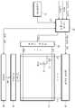
도 1은 본 발명의 일 실시 예에 따른 표시 장치를 나타내는 블록도이다.1 is a block diagram showing a display device according to an embodiment of the present invention.
도 1을 참조하면, 표시 장치는 표시 패널(10), 패널 구동부(20,30), 타이밍 컨트롤러(40), 오실레이터(ocillator)(70), 백라이트(80), 및 인버터(90)를 포함한다.1, the display device includes a
상기 표시 패널(10)은 서로 교차하는 복수의 게이트 라인(GL1 내지 GLm), 복수의 데이터 라인(DL1 내지 DLn), 이들의 교차 지점에 형성되는 박막 트랜지스터들(13), 및 상기 박막 트랜지스터들(13)에 접속된 액정 커패시터들(15)을 포함한 다. 상기 박막 트랜지스터들(13)은 도시되지 않았지만 상기 복수의 게이트 라인(GL1 내지 GLm)으로부터 분기된 게이트 전극, 절연층을 사이에 두고 상기 게이트 전극 위에 배치된 반도체층, 상기 복수의 데이터 라인(DL1 내지 DLn)으로부터 분기된 소스 전극, 및 상기 소스 전극에 대향하는 드레인 전극을 포함한다. 이러한 상기 박막 트랜지스터들(13)은 상기 액정 커패시터들(15)을 제어한다.The
상기 패널 구동부(20,30)는 게이트 구동부(20)와 데이터 구동부(30)를 포함한다.The
상기 게이트 구동부(20)는 상기 타이밍 컨트롤러(40)에서 생성된 게이트 제어 신호(GCS)에 응답하여 상기 복수의 게이트 라인(GL1 내지 GLm)에 순차적으로 스캔 신호를 공급한다. 상기 스캔 신호에 의해 상기 복수의 게이트 라인(GL1 내지 GLm)에 연결된 상기 박막 트랜지스터(13)가 턴-온 된다.The
상기 데이터 구동부(30)는 상기 타이밍 컨트롤러(40)에서 생성된 데이터 제어 신호(DCS)에 응답하여 데이터 신호를 상기 복수의 데이터 라인(DL1 내지 DLn)에 공급한다.The
상기 타이밍 컨트롤러(40)는 수평 동기 신호(H_sync), 상기 표시 패널(10)의 프레임 주파수를 결정하는 수직 동기 신호(V_sync), 화상 데이터(I_DATA), 메인 클럭(MCLK), 및 기준 클럭(OSC)을 수신한다. 상기 타이밍 컨트롤러(40)는 상기 데이터 구동부(30)에서 요구되는 형식에 맞게 상기 화상 데이터(I_DATA)를 변환하여 상기 데이터 구동부(30)에 화소 데이터(RGB_DATA)를 공급한다. 상기 타이밍 컨트롤러(40)는 상기 게이트 구동부(20)를 제어하는 게이트 제어 신호(GCS)와 상기 데이 터 구동부(30)를 제어하는 상기 데이터 제어 신호(DCS)를 각각 상기 게이트 구동부(20)와 상기 데이터 구동부(30)에 제공한다. 또한, 상기 타이밍 컨트롤러(40)는 상기 기준 클럭(OSC)에 근거하여 상기 수평 동기 신호(H_sync)와 상기 수직 동기 신호(V_sync)를 변조하고, 상기 수평 동기 신호(H_sync)와 상기 수직 동기 신호(V_sync)를 근거하여 상기 인버터(90)에 디밍 신호(BDS)와 백라이트 구동 신호(BOS)를 제공한다.The
상기 오실레이터(70)는 상기 기준 클럭(OSC)을 생성하여 상기 타이밍 컨트롤러(40)로 제공한다.The
상기 백라이트(80)는 상기 표시 패널(10)의 하측에 위치하며, 외부로부터 공급받은 전원을 이용하여 상기 표시 패널(10)에 광을 제공한다. 상기 백라이트(80)는 상기 디밍 신호(BDS)에 응답하여 휘도를 제어하는 복수의 램프를 포함할 수 있다.The
상기 인버터(90)는 외부의 휘도 제어 명령에 따라 펄스폭 변조(Pulse Width Modulation: PWM) 방식으로 상기 백라이트(80)에 인가되는 백라이트 전류(Ilamp)를 제어하여 상기 백라이트(80)의 휘도를 조절한다. 예를 들어, 상기 인버터(90)는 상기 타이밍 컨트롤러(40)에서 공급되는 디밍 신호(BDS)를 이용하여 상기 백라이트 전류(Ilamp)를 제어할 수 있다.The
이하에서는 도 2를 참조하여 상기 타이밍 컨트롤러를 자세히 설명한다. 도 2는 도 1에 도시된 타이밍 컨트롤러를 나타내는 블록도이다.Hereinafter, the timing controller will be described in detail with reference to FIG. 2 is a block diagram showing the timing controller shown in Fig.
타이밍 컨트롤러(40)는 메모리(41), 검출부(43), 비교부(45), 및 인버터 동 기부(49)를 포함한다.The
상기 메모리(41)는 상기 타이밍 컨트롤러(40)에서 EEPROM으로 형성된다. 상기 메모리(41)는 인버터에 공급되어 백라이트의 휘도를 제어하는 디밍 신호의 주파수(이하, 디밍 신호 주파수)(BDS)가 미리 저장된다. 상기 메모리(41)는 상기 디밍 신호 주파수(BDS_freq)를 상기 비교부(45)로 공급한다.The
상기 검출부(43)는 상기 수직 동기 신호(V_sync)와 상기 기준 클럭(OSC)을 수신한다. 상기 검출부(43)는 상기 기준 클럭(OSC)을 이용하여 상기 수직 동기 신호의 주파수(이하, 수직 동기 신호 주파수)(V_sync_freq)를 검출한다. 예를 들어, 상기 수직 동기 신호(V_sync)를 1Hz의 상기 기준 클럭(OSC)으로 카운트하여 상기 수직 동기 신호 주파수(V_sync_freq)를 검출한다. 상기 검출부(43)는 상기 수직 동기 신호 주파수(V_sync_freq)를 상기 비교부(45)로 공급한다.The
상기 비교부(45)는 메인 클럭(MCLK), 상기 디밍 신호 주파수(BDS_freq), 및 상기 수직 동기 신호 주파수(V_sync_freq)를 수신한다. 상기 비교부(45)는 상기 메인 클럭(MCLK)에 동기하여 상기 디밍 신호 주파수(BDS_freq)를 상기 수직 동기 신호 주파수(V_sync_freq)로 나누고, 그 결과값(V_div,V_mul)을 상기 인버터 동기부(49)로 출력한다. 상기 결과값(V_div,V_mul)은 상기 디밍 신호 주파수(BDS_freq)를 상기 수직 동기 신호 주파수(V_sync_freq)로 나누는 분수 형태의 분모값(V_div)과 분자값(V_mul)을 포함한다. 상기 비교부(45)는 상기 분모값(V_div)과 상기 분자값(V_mul)이 저장된 제1 룩업 테이블(46)과 제2 룩업 테이블(47)을 포함한다.The
(V_div)Denominator value
(V_div)
디밍 신호 주파수
Dimming
(V_mul)Molecular value
(V_mul)
디밍 신호 주파수
Dimming
표 1은 상기 분모값(V_div)이 저장된 상기 제1 룩업 테이블(46)이고, 표 2는 상기 분자값(V_mul)이 저장된 상기 제2 룩업 테이블(47)이다.Table 1 shows the first lookup table 46 in which the denominator value V_div is stored and Table 2 shows the second lookup table 47 in which the molecular value V_mul is stored.
표 1과 표 2에서 상기 제1 룩업 테이블(46)과 상기 제2 룩업 테이블(47)은 상기 디밍 신호 주파수(BDS_freq)와 상기 수직 동기 신호 주파수(V_sync_freq)의 범위에 대응하는 사이즈를 갖는다. 예를 들어, 상기 디밍 신호 주파수(BDS_freq)와 상기 수직 동기 신호 주파수(V_sync_freq)가 각각 0 ~ 200Hz의 범위에서 20Hz 단위로 구분된다. 또한, 상기 분모값(V_div)과 상기 분자값(V_mul)은 각각 1 ~ 15까지 설정될 수 있다.In Table 1 and Table 2, the first lookup table 46 and the second lookup table 47 have a size corresponding to the range of the dimming signal frequency BDS_freq and the vertical synchronizing signal frequency V_sync_freq. For example, the dimming signal frequency BDS_freq and the vertical synchronization signal frequency V_sync_freq are divided into 0 Hz to 200 Hz and 20 Hz units, respectively. In addition, the denominator value V_div and the molecular value V_mul may be set to 1 to 15, respectively.
상기 비교부(45)는 수신된 상기 수직 동기 신호 주파수(V_sync_freq)와 상기 디밍 신호 주파수(BDS_freq)를 상기 제1 룩업 테이블(46)과 상기 제2 룩업 테이블(47)에 적용하여 각각 상기 분모값(V_div)과 상기 분자값(V_mul)을 독출한다. 예를 들어, 상기 수직 동기 신호 주파수(V_sync_freq)가 120Hz이고 상기 디밍 신호 주파수(BDS_freq)가 160Hz일 경우 상기 분모값(V_div)은 3이고, 상기 분자값(V_mul)은 4이다. 또한, 상기 비교부(45)는 상기 분모값(V_div)과 상기 분자값(V_mul)을 상기 인버터 동기부(49)로 공급한다.The
상기 인버터 동기부(49)는 상기 메인 클럭(MCLK), 상기 수직 동기 신호(V_sync), 상기 분모값(V_div), 및 상기 분자값(V_mul)을 수신한다. 상기 인버터 동기부(49)는 상기 메인 클럭(MCLK)에 동기하여 상기 분모값(V_div)과 상기 분자값(V_mul)을 근거로 상기 수직 동기 신호(V_sync)를 변조한다. 상기 인버터 동기부(49)는 상기 수직 동기 신호(V_sync)를 변조하여 상기 디밍 신호(BDS)를 생성한다. 상기 수직 동기 신호(V_sync)는 다음의 수학식 1을 통해 변조할 수 있다.The
수학식 1에서 Freq(BDS)는 상기 디밍 신호(BDS)의 주파수이고, Freq(V_sync)는 상기 수직 동기 신호(V_sync)의 주파수이다. 또한, 수학식 1에서 V_mul은 상기 결과값의 분자값이고, V_div는 상기 결과값의 분모값이다.Freq (BDS) is the frequency of the dimming signal (BDS), and Freq (V_sync) is the frequency of the vertical synchronization signal (V_sync). In Equation (1), V_mul is a molecular value of the resultant value, and V_div is a denominator of the resultant value.
예를 들어, 상기 인버터 동기부(49)는 120Hz의 주파수를 갖는 상기 수직 동기 신호(V_sync)에 상기 분모값(V_div)과 상기 분자값(V_mul)에 근거한 4/3을 곱하여 160Hz의 주파수를 갖는 상기 디밍 신호(BDS)를 생성한다. 이러한 상기 인버터 동기부(49)는 상기 디밍 신호(BDS)를 인버터로 공급한다.For example, the
상기 디밍 신호(BDS)와 상기 수직 동기 신호(V_sync)가 동기되어, 백라이트의 휘도가 표시 패널의 영상에 따라 효과적으로 제어될 수 있다. 또한, 입력되는 상기 수직 동기 신호(V_sync)의 주파수가 변경되어도 상기 수직 동기 신호(V_sync)를 용이하게 변조하여 상기 디밍 신호(BDS)를 생성할 수 있다.The dimming signal BDS and the vertical synchronization signal V sync are synchronized so that the brightness of the backlight can be effectively controlled according to the image of the display panel. Also, even if the frequency of the input vertical synchronization signal V_sync is changed, the vertical synchronization signal V_sync can be easily modulated to generate the dimming signal BDS.
한편, 도 1에 도시된 수평 동기 신호(H_sync)와 백라이트 구동 신호(BOS)도 상술한 상기 타이밍 컨트롤러(40)를 이용하여 상기 수직 동기 신호(V_sync)와 상기 디밍 신호(BDS)와 같이 동기시킬 수 있다. 이에 대한 상세할 설명은 생략한다.Meanwhile, the horizontal synchronizing signal H_sync and the backlight driving signal BOS shown in FIG. 1 are synchronized with the vertical synchronizing signal V_sync and the dimming signal BDS using the
이하에서는 도 3 및 도 4를 참조하여 타이밍 컨트롤러의 동작을 더 상세히 설명한다. 도 3 및 도 4는 도 2에 도시된 타이밍 컨트롤러의 동작을 설명하기 위해 도시한 타이밍도이다.Hereinafter, the operation of the timing controller will be described in more detail with reference to FIGS. 3 and 4. FIG. FIGS. 3 and 4 are timing charts for explaining the operation of the timing controller shown in FIG. 2. FIG.
외부에서 타이밍 컨트롤러로 소정의 프레임 정보를 포함하는 수직 동기 신호(V_sync)가 공급된다. 상기 타이밍 컨트롤러는 상기 수직 동기 신호(V_sync)를 1Hz의 기준 클럭(OSC)으로 카운트하여 120Hz의 수직 동기 신호 주파수(V_sync_freq)를 검출한다. 상기 타이밍 컨트롤러는 160Hz로 미리 저장된 디밍 신호 주파수(BDS_freq)와 상기 수직 동기 신호 주파수(V_sync_freq)를 제1 룩업 테이블과 제2 룩업 테이블에서 비교하여 각각 상기 수직 동기 신호(V_sync)를 변조하기 위한 분수 형태의 배수를 독출한다. 상기 배수는 예컨대, 160Hz를 120Hz로 나눈 4/3이다. 이를 통해, 상기 타이밍 컨트롤러는 상기 배수를 근거로 상기 수직 동기 신호(V_sync)를 변조하여 160Hz의 주파수를 갖는 디밍 신호(BDS)를 생성한다.A vertical synchronization signal V_sync including predetermined frame information is supplied from the outside to the timing controller. The timing controller counts the vertical synchronization signal V_sync to a reference clock OSC of 1 Hz and detects a vertical synchronization signal frequency V_sync_freq of 120 Hz. The timing controller compares the dimming signal frequency (BDS_freq) and the vertical synchronization signal frequency (V_sync_freq) previously stored at 160 Hz in a first lookup table and a second lookup table to form a fractional signal form for modulating the vertical synchronization signal (V_sync) . The multiple is 4/3, for example, 160 Hz divided by 120 Hz. Accordingly, the timing controller generates a dimming signal (BDS) having a frequency of 160 Hz by modulating the vertical synchronization signal (V_sync) based on the multiple.
상기 타이밍 컨트롤러는 입력되는 상기 수직 동기 신호(V_sync)에 따라 상기 배수를 간단히 독출할 수 있고, 원하는 상기 디밍 신호(BDS)를 용이하게 생성할 수 있다.The timing controller can simply read the drain according to the inputted vertical synchronization signal V_sync and can easily generate the desired dimming signal BDS.
도 1은 본 발명의 일 실시 예에 따른 표시 장치를 나타내는 블록도이다.1 is a block diagram showing a display device according to an embodiment of the present invention.
도 2는 도 1에 도시된 타이밍 컨트롤러를 나타내는 블록도이다.2 is a block diagram showing the timing controller shown in Fig.
도 3 및 도 4는 도 2에 도시된 타이밍 컨트롤러의 동작을 설명하기 위해 도시한 타이밍도이다.FIGS. 3 and 4 are timing charts for explaining the operation of the timing controller shown in FIG. 2. FIG.
Claims (14)
Translated fromKoreanPriority Applications (2)
| Application Number | Priority Date | Filing Date | Title |
|---|---|---|---|
| KR1020080086963AKR101497651B1 (en) | 2008-09-03 | 2008-09-03 | Display device and driving method thereof |
| US12/473,879US8300004B2 (en) | 2008-09-03 | 2009-05-28 | Display apparatus and driving method thereof synchronizing frequencies of a synchronization signal and dimming signal |
Applications Claiming Priority (1)
| Application Number | Priority Date | Filing Date | Title |
|---|---|---|---|
| KR1020080086963AKR101497651B1 (en) | 2008-09-03 | 2008-09-03 | Display device and driving method thereof |
Publications (2)
| Publication Number | Publication Date |
|---|---|
| KR20100027873A KR20100027873A (en) | 2010-03-11 |
| KR101497651B1true KR101497651B1 (en) | 2015-03-06 |
Family
ID=41724715
Family Applications (1)
| Application Number | Title | Priority Date | Filing Date |
|---|---|---|---|
| KR1020080086963AExpired - Fee RelatedKR101497651B1 (en) | 2008-09-03 | 2008-09-03 | Display device and driving method thereof |
Country Status (2)
| Country | Link |
|---|---|
| US (1) | US8300004B2 (en) |
| KR (1) | KR101497651B1 (en) |
Families Citing this family (14)
| Publication number | Priority date | Publication date | Assignee | Title |
|---|---|---|---|---|
| US20120062605A1 (en)* | 2010-09-09 | 2012-03-15 | Ovidiu Aioanei | Led backlight dimming control for lcd applications |
| KR101963784B1 (en)* | 2011-07-20 | 2019-08-01 | 엘지디스플레이 주식회사 | Apparatus and method for driving back light, liquid crystal display device and driving method the same |
| CN102890917B (en)* | 2011-07-20 | 2015-09-02 | 乐金显示有限公司 | Backlight drive device and driving method, liquid crystal display and driving method thereof |
| US20140139504A1 (en)* | 2012-11-22 | 2014-05-22 | Shenzhen China Star Optoelectronics Technology Co., Ltd | Method for displaying flicker pattern, method for adjusting common voltage, and lcd module |
| CN103077692B (en)* | 2013-02-05 | 2015-09-09 | 深圳市华星光电技术有限公司 | The liquid crystal display control circuit of liquid crystal display driving method and use the method |
| KR102234512B1 (en)* | 2014-05-21 | 2021-04-01 | 삼성디스플레이 주식회사 | Display device, electronic device having display device and method of driving the same |
| KR102453288B1 (en)* | 2015-10-30 | 2022-10-11 | 엘지디스플레이 주식회사 | Liquid crystal display and dimming control method therof |
| KR102366556B1 (en)* | 2018-10-11 | 2022-02-22 | 매그나칩 반도체 유한회사 | Display driver ic controlling oscillator frequency and method thereof |
| TWI723669B (en)* | 2019-12-06 | 2021-04-01 | 新唐科技股份有限公司 | Backlight device and driving method |
| CN111429850A (en) | 2020-04-08 | 2020-07-17 | 深圳市华星光电半导体显示技术有限公司 | Display panel and display method thereof |
| US11823612B2 (en)* | 2021-09-17 | 2023-11-21 | Apple Inc. | Current load transient mitigation in display backlight driver |
| WO2023115569A1 (en)* | 2021-12-24 | 2023-06-29 | 京东方科技集团股份有限公司 | Backlight control chip, driving method, backlight control system, and near-eye display device |
| CN114677978B (en)* | 2022-04-01 | 2022-09-20 | 北京芯格诺微电子有限公司 | LED backlight driving method for brightness abnormity caused by frame synchronization signal switching |
| KR102702436B1 (en)* | 2022-04-26 | 2024-09-05 | 엘지전자 주식회사 | Display device and operating method thereof |
Citations (4)
| Publication number | Priority date | Publication date | Assignee | Title |
|---|---|---|---|---|
| KR20040002746A (en)* | 2002-06-27 | 2004-01-07 | 후지쯔 디스플레이 테크놀로지스 코포레이션 | Driving method of liquid crystal display device and driving control circuit, and liquid crystal display device having the same |
| KR20040045396A (en)* | 2001-10-23 | 2004-06-01 | 마쯔시다덴기산교 가부시키가이샤 | Liquid crystal display apparatus and drive method thereof |
| KR20070062016A (en)* | 2005-12-12 | 2007-06-15 | 엘지전자 주식회사 | Dimming circuit for image display device and its control method |
| KR20070110037A (en)* | 2005-01-25 | 2007-11-15 | 마츠시타 덴끼 산교 가부시키가이샤 | Backlight Control and Display |
Family Cites Families (6)
| Publication number | Priority date | Publication date | Assignee | Title |
|---|---|---|---|---|
| CN100412919C (en)* | 2002-05-28 | 2008-08-20 | 皇家飞利浦电子股份有限公司 | Reduce motion blur at varying duty cycles |
| TWI396469B (en)* | 2002-09-04 | 2013-05-11 | Samsung Display Co Ltd | Inverter for liquid crystal display |
| EP1921595A3 (en)* | 2003-09-30 | 2008-08-06 | LG Electronics Inc. | Method and apparatus of driving a plasma display panel |
| JP2005316298A (en) | 2004-04-30 | 2005-11-10 | Nec Lcd Technologies Ltd | Liquid crystal display device, light source driving circuit and light source driving method used for the liquid crystal display device |
| KR101177568B1 (en) | 2005-03-30 | 2012-08-27 | 엘지디스플레이 주식회사 | Liquid Crystal Display device and driving method thereof |
| US7746330B2 (en)* | 2005-12-22 | 2010-06-29 | Au Optronics Corporation | Circuit and method for improving image quality of a liquid crystal display |
- 2008
- 2008-09-03KRKR1020080086963Apatent/KR101497651B1/ennot_activeExpired - Fee Related
- 2009
- 2009-05-28USUS12/473,879patent/US8300004B2/ennot_activeExpired - Fee Related
Patent Citations (4)
| Publication number | Priority date | Publication date | Assignee | Title |
|---|---|---|---|---|
| KR20040045396A (en)* | 2001-10-23 | 2004-06-01 | 마쯔시다덴기산교 가부시키가이샤 | Liquid crystal display apparatus and drive method thereof |
| KR20040002746A (en)* | 2002-06-27 | 2004-01-07 | 후지쯔 디스플레이 테크놀로지스 코포레이션 | Driving method of liquid crystal display device and driving control circuit, and liquid crystal display device having the same |
| KR20070110037A (en)* | 2005-01-25 | 2007-11-15 | 마츠시타 덴끼 산교 가부시키가이샤 | Backlight Control and Display |
| KR20070062016A (en)* | 2005-12-12 | 2007-06-15 | 엘지전자 주식회사 | Dimming circuit for image display device and its control method |
Also Published As
| Publication number | Publication date |
|---|---|
| KR20100027873A (en) | 2010-03-11 |
| US20100053228A1 (en) | 2010-03-04 |
| US8300004B2 (en) | 2012-10-30 |
Similar Documents
| Publication | Publication Date | Title |
|---|---|---|
| KR101497651B1 (en) | Display device and driving method thereof | |
| EP2149872B1 (en) | Method and apparatus for driving a backlight assembly | |
| TWI459092B (en) | Liquid crystal display and scanning back light driving method thereof | |
| US8363004B2 (en) | Method of driving a light source, light source device for performing the same, and display device having the light source device | |
| JP5529500B2 (en) | Display device and method for driving the display device | |
| TWI418879B (en) | Liquid crystal display and method of driving the same | |
| JP3027298B2 (en) | Liquid crystal display with backlight control function | |
| CN108109602B (en) | Display device | |
| US20130076769A1 (en) | Liquid crystal display device | |
| KR20130133519A (en) | Backlight driver of liquid crystal display device and method for driving the same | |
| US20140362292A1 (en) | Display device and driving method thereof | |
| US8289268B2 (en) | Apparatus and method for improving video quality of display device | |
| US20070159447A1 (en) | LCD capable of controlling luminance of screen and method for controlling luminance thereof | |
| US7746330B2 (en) | Circuit and method for improving image quality of a liquid crystal display | |
| KR100523598B1 (en) | Method for controlling brightness and implementing low power mode of back light unit in an liquid crystal display | |
| JP2009294499A (en) | Liquid crystal display device and liquid crystal display controller | |
| KR101385461B1 (en) | Liquid crystal display and method for driving the same | |
| KR101131306B1 (en) | Back light unit of liquid crystal display device | |
| KR101647031B1 (en) | Liquid crystal display device | |
| KR101296568B1 (en) | Device for regulating a brightness, method thereof and liquid crystal display module having the same | |
| US7511434B2 (en) | Lamp driving apparatus, liquid crystal display comprising the same, and driving method thereof | |
| KR101761253B1 (en) | liquid crystal display device and method of driving the same | |
| TWI406233B (en) | Liquid crystal display panel, liquid crystal display apparatus and control method thereof | |
| KR20050054332A (en) | Liquid crystal display and driving method thereof | |
| KR100556663B1 (en) | Low power mode implementation method of backlight for liquid crystal display |
Legal Events
| Date | Code | Title | Description |
|---|---|---|---|
| PA0109 | Patent application | St.27 status event code:A-0-1-A10-A12-nap-PA0109 | |
| PG1501 | Laying open of application | St.27 status event code:A-1-1-Q10-Q12-nap-PG1501 | |
| R18-X000 | Changes to party contact information recorded | St.27 status event code:A-3-3-R10-R18-oth-X000 | |
| N231 | Notification of change of applicant | ||
| PN2301 | Change of applicant | St.27 status event code:A-3-3-R10-R13-asn-PN2301 St.27 status event code:A-3-3-R10-R11-asn-PN2301 | |
| A201 | Request for examination | ||
| PA0201 | Request for examination | St.27 status event code:A-1-2-D10-D11-exm-PA0201 | |
| E902 | Notification of reason for refusal | ||
| PE0902 | Notice of grounds for rejection | St.27 status event code:A-1-2-D10-D21-exm-PE0902 | |
| E13-X000 | Pre-grant limitation requested | St.27 status event code:A-2-3-E10-E13-lim-X000 | |
| P11-X000 | Amendment of application requested | St.27 status event code:A-2-2-P10-P11-nap-X000 | |
| P13-X000 | Application amended | St.27 status event code:A-2-2-P10-P13-nap-X000 | |
| E701 | Decision to grant or registration of patent right | ||
| PE0701 | Decision of registration | St.27 status event code:A-1-2-D10-D22-exm-PE0701 | |
| R17-X000 | Change to representative recorded | St.27 status event code:A-3-3-R10-R17-oth-X000 | |
| GRNT | Written decision to grant | ||
| PR0701 | Registration of establishment | St.27 status event code:A-2-4-F10-F11-exm-PR0701 | |
| PR1002 | Payment of registration fee | St.27 status event code:A-2-2-U10-U11-oth-PR1002 Fee payment year number:1 | |
| PG1601 | Publication of registration | St.27 status event code:A-4-4-Q10-Q13-nap-PG1601 | |
| R18-X000 | Changes to party contact information recorded | St.27 status event code:A-5-5-R10-R18-oth-X000 | |
| LAPS | Lapse due to unpaid annual fee | ||
| PC1903 | Unpaid annual fee | St.27 status event code:A-4-4-U10-U13-oth-PC1903 Not in force date:20180225 Payment event data comment text:Termination Category : DEFAULT_OF_REGISTRATION_FEE | |
| PC1903 | Unpaid annual fee | St.27 status event code:N-4-6-H10-H13-oth-PC1903 Ip right cessation event data comment text:Termination Category : DEFAULT_OF_REGISTRATION_FEE Not in force date:20180225 | |
| R18-X000 | Changes to party contact information recorded | St.27 status event code:A-5-5-R10-R18-oth-X000 |