KR101497405B1 - Touch panel input apparatus and input detection method thereof - Google Patents
Touch panel input apparatus and input detection method thereofDownload PDFInfo
- Publication number
- KR101497405B1 KR101497405B1KR1020130093530AKR20130093530AKR101497405B1KR 101497405 B1KR101497405 B1KR 101497405B1KR 1020130093530 AKR1020130093530 AKR 1020130093530AKR 20130093530 AKR20130093530 AKR 20130093530AKR 101497405 B1KR101497405 B1KR 101497405B1
- Authority
- KR
- South Korea
- Prior art keywords
- driving signal
- pulses
- signal
- period
- sensing
- Prior art date
- Legal status (The legal status is an assumption and is not a legal conclusion. Google has not performed a legal analysis and makes no representation as to the accuracy of the status listed.)
- Active
Links
Images


Classifications
- G—PHYSICS
- G06—COMPUTING OR CALCULATING; COUNTING
- G06F—ELECTRIC DIGITAL DATA PROCESSING
- G06F3/00—Input arrangements for transferring data to be processed into a form capable of being handled by the computer; Output arrangements for transferring data from processing unit to output unit, e.g. interface arrangements
- G06F3/01—Input arrangements or combined input and output arrangements for interaction between user and computer
- G06F3/03—Arrangements for converting the position or the displacement of a member into a coded form
- G06F3/041—Digitisers, e.g. for touch screens or touch pads, characterised by the transducing means
- G06F3/0416—Control or interface arrangements specially adapted for digitisers
- G06F3/04166—Details of scanning methods, e.g. sampling time, grouping of sub areas or time sharing with display driving
- G—PHYSICS
- G06—COMPUTING OR CALCULATING; COUNTING
- G06F—ELECTRIC DIGITAL DATA PROCESSING
- G06F3/00—Input arrangements for transferring data to be processed into a form capable of being handled by the computer; Output arrangements for transferring data from processing unit to output unit, e.g. interface arrangements
- G06F3/01—Input arrangements or combined input and output arrangements for interaction between user and computer
- G06F3/03—Arrangements for converting the position or the displacement of a member into a coded form
- G06F3/041—Digitisers, e.g. for touch screens or touch pads, characterised by the transducing means
- G06F3/0416—Control or interface arrangements specially adapted for digitisers
- G06F3/04164—Connections between sensors and controllers, e.g. routing lines between electrodes and connection pads
- G—PHYSICS
- G06—COMPUTING OR CALCULATING; COUNTING
- G06F—ELECTRIC DIGITAL DATA PROCESSING
- G06F3/00—Input arrangements for transferring data to be processed into a form capable of being handled by the computer; Output arrangements for transferring data from processing unit to output unit, e.g. interface arrangements
- G06F3/01—Input arrangements or combined input and output arrangements for interaction between user and computer
- G06F3/03—Arrangements for converting the position or the displacement of a member into a coded form
- G06F3/033—Pointing devices displaced or positioned by the user, e.g. mice, trackballs, pens or joysticks; Accessories therefor
- G06F3/0354—Pointing devices displaced or positioned by the user, e.g. mice, trackballs, pens or joysticks; Accessories therefor with detection of 2D relative movements between the device, or an operating part thereof, and a plane or surface, e.g. 2D mice, trackballs, pens or pucks
- G—PHYSICS
- G06—COMPUTING OR CALCULATING; COUNTING
- G06F—ELECTRIC DIGITAL DATA PROCESSING
- G06F3/00—Input arrangements for transferring data to be processed into a form capable of being handled by the computer; Output arrangements for transferring data from processing unit to output unit, e.g. interface arrangements
- G06F3/01—Input arrangements or combined input and output arrangements for interaction between user and computer
- G06F3/03—Arrangements for converting the position or the displacement of a member into a coded form
- G06F3/041—Digitisers, e.g. for touch screens or touch pads, characterised by the transducing means
- G06F3/044—Digitisers, e.g. for touch screens or touch pads, characterised by the transducing means by capacitive means
- G06F3/0446—Digitisers, e.g. for touch screens or touch pads, characterised by the transducing means by capacitive means using a grid-like structure of electrodes in at least two directions, e.g. using row and column electrodes
- G—PHYSICS
- G06—COMPUTING OR CALCULATING; COUNTING
- G06F—ELECTRIC DIGITAL DATA PROCESSING
- G06F17/00—Digital computing or data processing equipment or methods, specially adapted for specific functions
- G06F17/10—Complex mathematical operations
- G06F17/16—Matrix or vector computation, e.g. matrix-matrix or matrix-vector multiplication, matrix factorization
Landscapes
- Engineering & Computer Science (AREA)
- General Engineering & Computer Science (AREA)
- Theoretical Computer Science (AREA)
- Human Computer Interaction (AREA)
- Physics & Mathematics (AREA)
- General Physics & Mathematics (AREA)
- Computer Networks & Wireless Communication (AREA)
- Position Input By Displaying (AREA)
Abstract
Translated fromKoreanDescription
Translated fromKorean본 발명은 터치패널 입력장치 및 그의 입력검출방법에 관한 것으로, 보다 상세하게는, 노이즈의 영향을 줄여 터치 감도를 향상시킬 수 있는 터치패널 입력장치 및 그의 입력검출방법에 관한 것이다.BACKGROUND OF THE
일반적으로, 전자통신 기술의 발전을 통해 다양한 전자기기들이 만들어지고 있다. 이러한 기기들은 점차 사용자의 조작 편의성과 디자인의 수려함을 강조하는 추세에 있는데, 이러한 추세에 따라 강조되는 것은 키보드 혹은 키패드로 대표되는 입력 장치의 다변화이다.In general, various electronic devices are being developed through the development of electronic communication technology. These devices are increasingly emphasizing the convenience of the user and ease of design. What is emphasized in this trend is the diversification of the input device represented by the keyboard or keypad.
입력 장치는 키보드 혹은 키패드 등의 입력 장치를 통한 데이터 처리 과정으로부터 발전하여, 입력 장치와 출력장치가 하나로 묶여 사용 가능한 터치 패널(Touch Panel)의 형태로까지 발전하였다. 터치 패널(Touch Panel)은 다른 입력기기 없이 디스플레이 장치의 화면을 터치함으로써 입력이 가능한 입력 장치를 통칭하는 것을 의미한다.The input device has developed from a process of data processing through an input device such as a keyboard or a keypad, and has developed into a touch panel type in which an input device and an output device can be bundled together. A touch panel refers to an input device that can be input by touching the screen of the display device without any other input device.
터치 패널은 형성된 복수의 노드캐패시터에 저장된 캐패시턴스를 감지하여 터치 입력 여부를 감지한다. 하지만, 터치 패널은 디스플레이 장치에서 발생된 노이즈 등의 영향으로 인해 노드캐패시터의 캐패시턴스가 변하게 됨으로써 오동작을 할 우려가 있다.The touch panel senses capacitance stored in a plurality of node capacitors formed and detects whether or not the touch input is performed. However, the capacitance of the node capacitor may change due to the influence of the noise generated in the display device, thereby causing a malfunction.
본 발명의 목적은 터치 패널의 노이즈의 영향을 줄여 터치 감도를 향상시킬 수 있는 터치 패널 입력장치 및 그의 터치 패널입력검출 방법을 제공하는 것이다.SUMMARY OF THE INVENTION It is an object of the present invention to provide a touch panel input device capable of reducing the influence of noise on a touch panel and improving touch sensitivity, and a touch panel input detection method thereof.
상기 목적을 달성하기 위하여 본 발명의 제1측면은, 복수의 노드캐패시터를 포함하며, 각 노드캐패시터는 복수의 구동신호전극 중 하나의 구동신호전극과 복수의 감지신호전극 중 하나의 감지신호전극에 의해 형성되는 터치 패널, 복수의 구동신호전극 중 적어도 2개의 구동신호전극에 각각 제1구동신호와 제2구동신호를 동시에 인가하되, 제1구간과 제2구간에서 제1구동신호와 상기 제2구동신호는 각각 복수의 펄스를 포함하고, 복수의 펄스 중 적어도 하나의 펄스의 폭은 다른 펄스의 폭과 다르고, 제2구동신호의 복수의 펄스 중 적어도 하나의 펄스는 제1구간과 제2구간 중 하나의 구간에서 제1구동신호의 복수의 펄스와 위상이 다른 구동신호공급부 및 제1구간과 제2구간에서 복수의 감지신호전극으로부터의 복수의 노드캐패시터 중 적어도 2개의 노드캐패시터의 캐패시턴스에 대한 정보를 포함하는 감지신호들을 수신하는 감지신호부를 포함하는 터치 패널 입력장치를 제공하는 것이다.In order to achieve the above object, a first aspect of the present invention is a display device including a plurality of node capacitors, wherein each of the node capacitors includes one of a plurality of drive signal electrodes and one of the plurality of sense signal electrodes A first driving signal and a second driving signal are simultaneously applied to at least two driving signal electrodes among a plurality of driving signal electrodes and a first driving signal and a second driving signal are applied in a first period and a second period, The driving signal includes a plurality of pulses, the width of at least one of the plurality of pulses is different from the width of the other pulses, and at least one of the plurality of pulses of the second driving signal is divided into a first period and a second period And a plurality of node capacitors from the plurality of sense signal electrodes in the first section and the plurality of sense electrodes in the second section, And a sensing signal unit for receiving sensing signals including information on capacitances of the capacitors.
부가적으로, 복수의 펄스 중 적어도 하나의 펄스는 하이 상태이고 또 다른 하나의 펄스는 로우 상태인 터치 패널 입력장치를 제공하는 것이다.Additionally, at least one of the plurality of pulses is in a high state and the other pulse is in a low state.
부가적으로, 하이 상태와 로우 상태는 펄스폭이 다른 터치 패널 입력장치를 제공하는 것이다.In addition, the high state and the low state provide a touch panel input device having different pulse widths.
부가적으로, 하이 상태와 로우 상태가 교번적으로 나타나는 터치 패널 입력장치를 제공하는 것이다.In addition, the present invention provides a touch panel input device in which a high state and a low state alternately appear.
부가적으로, 제2구간에서 상기 제1구동신호의 복수의 펄스 중 적어도 하나의 펄스의 듀티비는 제2구동신호의 복수의 펄스 중 적어도 하나의 펄스의 듀티비와 다른 터치 패널 입력장치를 제공하는 것이다.In addition, the duty ratio of at least one of the plurality of pulses of the first drive signal in the second section may be different from the duty ratio of at least one of the plurality of pulses of the second drive signal to provide a different touch panel input device .
부가적으로, 감지신호부는 제1구간과 제2구간에서 복수의 펄스의 수에 대응하여 감지신호를 수신하는 횟수를 결정하고, 수신된 감지신호들을 합산하여 노드캐패시터의 캐패시턴스에 대한 정보를 산출하는 터치 패널 입력장치를 제공하는 것이다.In addition, the sensing signal unit may determine the number of times the sensing signal is received corresponding to the number of pulses in the first and second intervals, and may calculate the information about the capacitance of the node capacitor by summing the sensing signals received And a touch panel input device.
부가적으로, 장치는 제어부를 더 포함하되, 제어부는 제1구간과 제2구간에 대응하는 코드들을 저장하는 메모리를 더 포함하고, 코드들에 의해 제1구동신호와 제2구동신호의 펄스의 형태가 결정되는 터치 패널 입력장치를 제공하는 것이다.Additionally, the apparatus further comprises a control section, wherein the control section further comprises a memory for storing codes corresponding to the first section and the second section, And the shape of the touch panel is determined.
본 발명의 제2측면은, 복수의 노드캐패시터를 포함하며, 각 노드캐패시터는 복수의 구동신호전극 중 하나의 구동신호전극과, 복수의 감지신호전극 중 하나의 감지신호전극에 의해 형성되는 터치 패널의 입력검출 방법에 있어서, 복수의 구동신호전극 중 적어도 2개의 구동신호전극에 각각 제1구동신호와 제2구동신호를 동시에 인가하되, 제1구동신호와 제2구동신호는 제1구간과 제2구간에서 각각 복수의 펄스를 포함하고, 복수의 펄스 중 적어도 하나의 펄스의 폭은 다른 펄스의 폭과 다르고, 제2구동신호의 복수의 펄스 중 적어도 하나의 펄스는 제1구간과 제2구간 중 하나의 구간에서 제1구동신호의 복수의 펄스와 위상이 다르게 인가되는 단계, 제1구간과 제2구간에서 복수의 감지신호전극으로부터 복수의 노드캐패시터 중 적어도 2개의 노드캐패시터의 캐패시턴스에 대한 정보를 포함하는 감지신호들을 감지신호검출부에서 수신하는 단계 및 감지신호검출부에서 적어도 2개의 노드캐패시터의 캐패시턴스에 대한 정보를 이용하여 터치 패널의 터치 정보를 추출하는 단계를 포함하는 터치 패널의 입력검출 방법을 제공하는 것이다.A second aspect of the present invention is a display device including a plurality of node capacitors, each of the node capacitors including one of a plurality of drive signal electrodes and a touch panel formed by one of the plurality of sense signal electrodes, A first driving signal and a second driving signal are simultaneously applied to at least two driving signal electrodes among a plurality of driving signal electrodes, and the first driving signal and the second driving signal are applied to the first section and the second section, respectively, Wherein a width of at least one of the plurality of pulses is different from a width of the other pulses and at least one pulse of the plurality of pulses of the second driving signal is divided into a first period and a second period, A plurality of node capacitors of a plurality of node capacitors from a plurality of sense signal electrodes in a first period and a second period, The method comprising the steps of: receiving sensing signals including information on capacitances in a sensing signal detector; and extracting touch information from a touch panel using information about capacitances of at least two node capacitors in a sensing signal detector And to provide an input detection method.
부가적으로, 하이 상태와 로우 상태는 펄스폭이 다른 터치 패널의 입력검출 방법을 제공하는 것이다.In addition, the high state and the low state provide a method of detecting an input of a touch panel having different pulse widths.
부가적으로, 복수의 펄스는 시간의 경과에 따라 펄스폭이 넓어지는 터치 패널의 입력검출방법을 제공하는 것이다.In addition, it is an object of the present invention to provide an input detection method of a touch panel in which a plurality of pulses have a wider pulse width as time elapses.
부가적으로, 제2구간에서 상기 제1구동신호의 복수의 펄스 중 적어도 하나의 펄스의 듀티비는 제2구동신호의 복수의 펄스 중 적어도 하나의 펄스의 듀티비와 다른 터치 패널의 입력검출방법을 제공하는 것이다.In addition, the duty ratio of at least one of the plurality of pulses of the first driving signal in the second period may be different from the duty ratio of at least one pulse of the plurality of pulses of the second driving signal, .
부가적으로, 감지신호검출부는 제1구간과 제2구간에서 복수의 펄스의 수에 대응하여 상기 감지신호를 수신하는 횟수를 결정하고, 수신된 감지신호들을 합산하여 노드캐패시터의 캐패시턴스에 대한 정보를 산출하는 터치 패널의 입력검출 방법을 제공하는 것이다.In addition, the sensing signal detector may determine the number of times the sensing signal is received corresponding to the number of pulses in the first and second sections, and may sum the received sensing signals to obtain information about the capacitance of the node capacitor And a method of detecting an input of a touch panel.
본 발명에 따른 터치패널 입력장치 및 그의 입력검출방법에 의하면, 높은 주파수 대역을 갖는 구동신호를 동시에 다수의 구동신호전극에 인가함으로써 터치패널의 복수의 지점을 동시에 인식할 수 있고 노이즈의 영향을 줄여 터치를 보다 더 정확히 인식할 수 있도록 할 수 있다.According to the touch panel input device and the input detection method of the present invention, it is possible to simultaneously recognize a plurality of points on the touch panel by applying a driving signal having a high frequency band to a plurality of driving signal electrodes at the same time, So that the touch can be recognized more accurately.
도 1은 본 발명에 따른 터치 패널 입력장치의 일 실시예를 나타내는 구조도이다.
도 2는 도 1에 채용된 구동신호공급부의 구성을 나타내는 도면이다.
도 3은 도 2에 도시된 구동신호공급부에서 생성되는 구동신호의 제1실시예를 나타내는 타이밍도이다.
도 4는 도 2에 도시된 구동신호공급부에서 생성되는 구동신호의 제2실시예를 나타내는 타이밍도이다.
도 5는 도 2에 도시된 구동신호공급부에서 생성되는 구동신호의 제3실시예를 나타내는 타이밍도이다.
도 6은 도 3에 도시된 구동신호의 파형의 다른 일실시예를 나타내는 타이밍도이다.
도 7은 도 1에 채용된 감지신호부의 구성을 나타내는 도면이다.
도 8은 도 1에 도시된 터치 패널에서 입력을 검출하는 방법을 나타내는 순서도이다.1 is a structural diagram showing an embodiment of a touch panel input device according to the present invention.
2 is a diagram showing a configuration of a drive signal supply unit employed in FIG.
3 is a timing chart showing a first embodiment of a drive signal generated in the drive signal supply unit shown in FIG.
4 is a timing chart showing a second embodiment of a drive signal generated in the drive signal supply unit shown in FIG.
5 is a timing chart showing a third embodiment of a drive signal generated by the drive signal supply unit shown in FIG.
6 is a timing chart showing another embodiment of the waveform of the drive signal shown in Fig.
FIG. 7 is a diagram showing a configuration of a sense signal unit employed in FIG. 1. FIG.
8 is a flowchart showing a method of detecting an input in the touch panel shown in Fig.
후술하는 본 발명에 대한 상세한 설명은, 본 발명이 실시될 수 있는 특정 실시예를 예시로서 도시하는 첨부 도면을 참조한다. 이들 실시예는 당업자가 본 발명을 실시할 수 있기에 충분하도록 상세히 설명된다. 본 발명의 다양한 실시예는 서로 다르지만 상호 배타적일 필요는 없음이 이해되어야 한다. 예를 들어, 여기에 기재되어 있는 특정 형상, 구조 및 특성은 일 실시예에 관련하여 본 발명의 정신 및 범위를 벗어나지 않으면서 다른 실시예로 구현될 수 있다. 또한, 각각의 개시된 실시예 내의 개별 구성요소의 위치 또는 배치는 본 발명의 정신 및 범위를 벗어나지 않으면서 변경될 수 있음이 이해되어야 한다. 따라서, 후술하는 상세한 설명은 한정적인 의미로서 취하려는 것이 아니며, 본 발명의 범위는, 적절하게 설명된다면, 그 청구항들이 주장하는 것과 균등한 모든 범위와 더불어 첨부된 청구항에 의해서만 한정된다. 도면에서 유사한 참조부호는 여러 측면에 걸쳐서 동일하거나 유사한 기능을 지칭한다.The following detailed description of the invention refers to the accompanying drawings, which illustrate, by way of illustration, specific embodiments in which the invention may be practiced. These embodiments are described in sufficient detail to enable those skilled in the art to practice the invention. It should be understood that the various embodiments of the present invention are different, but need not be mutually exclusive. For example, certain features, structures, and characteristics described herein may be implemented in other embodiments without departing from the spirit and scope of the invention in connection with an embodiment. It is also to be understood that the position or arrangement of the individual components within each disclosed embodiment may be varied without departing from the spirit and scope of the invention. The following detailed description is, therefore, not to be taken in a limiting sense, and the scope of the present invention is to be limited only by the appended claims, along with the full scope of equivalents to which such claims are entitled, if properly explained. In the drawings, like reference numerals refer to the same or similar functions throughout the several views.
이하, 첨부되는 도면을 참조하여 본 발명의 실시예에 따른 터치패널 입력장치 및 그의 터치패널 입력검출방법을 설명한다.Hereinafter, a touch panel input device and a touch panel input detection method according to an embodiment of the present invention will be described with reference to the accompanying drawings.
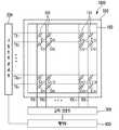
도 1은 본 발명에 따른 터치 패널 입력장치의 일 실시예를 나타내는 구조도이다.1 is a structural diagram showing an embodiment of a touch panel input device according to the present invention.
도 1을 참조하면, 터치 패널 입력장치(1000)는 복수의 노드캐패시터(101)를 포함하며, 각 노드캐패시터(101)는 복수의 구동신호전극(TX1,TX2,…,TXn-1,TXn) 중 하나의 구동신호전극과 복수의 감지신호전극(RX1,RX2,…,RXn-1,RXn) 중 하나의 감지신호전극에 의해 형성될 수 있는 터치패널(100)과, 복수의 구동신호전극(TX1,TX2,…,TXn-1,TXn) 중 적어도 2개의 구동신호전극에 각각 제1구동신호와 제2구동신호를 동시에 인가하되, 제1구간과 제2구간에서 제1구동신호와 제2구동신호는 각각 복수의 펄스를 포함하고, 복수의 펄스 중 적어도 하나의 펄스는 폭이 다른 펄스의 폭과 다르고, 제2구동신호의 복수의 펄스 중 적어도 하나의 펄스는 제1구간과 제2구간 중 하나의 구간에서 제1구동신호의 복수의 펄스와 위상이 다른 구동신호공급부 (200)와, 적어도 제1구간과 제2구간에서 복수의 감지신호전극(RX1,RX2,…,RXn-1,RXn)으로부터의 복수의 노드캐패시터(101) 중 적어도 2개의 노드캐패시터의 캐패시턴스에 대한 정보를 포함하는 감지신호들을 수신하는 감지신호부(300)를 포함할 수 있다.1, a touch
터치패널(100)은 복수의 구동신호전극(TX1,TX2,…,TXn-1,TXn)과 복수의 감지신호전극(RX1,RX2,…,RXn-1,RXn)을 포함하며, 디스플레이부(500)의 상부 또는 내부에 배치되어 있을 수 있다. 하지만, 터치패널(100)의 위치는 이에 한정되는 것은 아니다. 터치패널(100)이 형성되는 디스플레이부(500)는 액정표시장치(Liquid Crystal Display: LCD), 유기발광 표시장치(Organic Light Emitting Diode: OLED) 등을 예로 들을 수 있다. 하지만, 이에 한정되는 것은 아니다.The
이하의 설명 및 첨부되는 도면에서는 터치패널(100)의 복수의 구동신호전극(TX1,TX2,…,TXn-1,TXn)과 복수의 감지신호전극(RX1,RX2,…,RXn-1,RXn)이 직교 어레이를 구성하는 것으로 도시되어 있지만, 본 발명은 이에 한정되지 않으며, 복수의 구동신호전극(TX1,TX2,…,TXn-1,TXn)과 복수의 감지신호전극(RX1,RX2,…,RXn-1,RXn)이 대각선, 동심원 및 3차원 랜덤 배열 등을 비롯한 임의의 수의 차원 및 이의 응용 배열을 갖도록 할 수 있다. 복수의 구동신호전극(TX1,TX2,…,TXn-1,TXn)과 복수의 감지신호전극 (RX1,RX2,…,RXn-1,RXn)은 투명 전도성 물질(예를 들면, ITO(Indium Tin Oxide) 또는 ATO(Antimony Tin Oxide)) 등으로 형성될 수 있다. 그러나 이에 한정되지 않고, 복수의 구동신호전극(TX1,TX2,…,TXn-1,TXn)과 복수의 감지신호전극(RX1,RX2,…,RXn-1,RXn)은 다른 투명 물질 또는 구리 등의 불투명 전도성 물질로 형성될 수도 있다. 또한, 복수의 구동신호전극(TX1,TX2,…,TXn-1,TXn)과 복수의 감지신호전극(RX1,RX2,…,RXn-1,RXn)의 수가 동일한 것으로 되어 있지만 이에 한정되는 것은 아니며, 터치패널(100)의 모양에 따라 달라질 수 있다.In the following description and accompanying drawings, a plurality of driving signal electrodes TX1, TX2, ... TXn-1, TXn and a plurality of sensing signal electrodes RX1, RX2, ..., RXn-1, RXn The present invention is not limited to this, and a plurality of driving signal electrodes TX1, TX2, ..., TXn-1, TXn and a plurality of sensing signal electrodes RX1, RX2, ..., RX2 may be formed. , RXn-1, RXn) may have any number of dimensions, including diagonal, concentric and three-dimensional random arrays, and their application arrangements. The plurality of driving signal electrodes TX1 to TXn and the plurality of sensing signal electrodes RX1 to RXn are formed of a transparent conductive material such as ITO Oxide) or ATO (antimony tin oxide)). However, the present invention is not limited thereto, and the plurality of driving signal electrodes TX1, TX2, ..., TXn-1, TXn and the plurality of sensing signal electrodes RX1, RX2, ..., RXn- Of opaque conductive material. The number of the plurality of driving signal electrodes TX1, TX2, ..., TXn-1, TXn and the number of the plurality of sensing signal electrodes RX1, RX2, ..., RXn-1, RXn is the same, , And the shape of the
터치패널(100)에서 복수의 노드캐패시터들(101)은 복수의 구동신호전극(TX1,TX2,…,TXn-1,TXn)과 복수의 감지신호전극(RX1,RX2,…,RXn-1,RXn)에 의해 생성될 수 있다. 여기서, 복수의 구동신호전극(TX1,TX2,…,TXn-1,TXn)과 복수의 감지신호전극(RX1,RX2,…,RXn-1,RXn)을 각각 선으로 표시하였지만 실제로는 전극 패턴으로 구현될 수 있다. 또한, 복수의 구동신호전극(TX1,TX2,…,TXn-1,TXn)과 복수의 감지신호전극(RX1,RX2,…,RXn-1,RXn)의 전극의 폭은 다를 수도 있다.The plurality of
구동신호공급부(200)는 복수의 구동신호전극(TX1,TX2,…,TXn-1,TXn)에 구동신호를 인가한다. 구동신호공급부(200)는 터치패널(100)에 형성되어 있는 복수의 구동신호전극(TX1,TX2,…,TXn-1,TXn)에 구동신호들이 인가되면, 노드캐패시터들(101)의 일단에 구동신호가 인가될 수 있다. 구동신호가 인가된다는 것은 펄스가 발생되어 구동신호전극(TX1,TX2,…,TXn-1,TXn)에 전달되는 것을 의미할 수 있다. 또한, 펄스는 하이 상태일수도 있고 로우 상태일 수도 있다. 또한, 구동신호공급부(200)에서 인가하는 구동신호들은 하나의 구간에서 동시에 복수의 구동신호전극들(TX1,TX2,…,TXn-1,TXn) 중 적어도 2개의 구동신호전극에 구동신호가 인가되도록 할 수 있다. 여기서, "동시" 라는 것은 완전 동일한 시점에 구동신호를 적어도 2개의 구동신호전극에 인가되는 것만을 의미하는 것은 아니며, 어느 정도 시간차를 가지고 인가되는 것도 포함할 수 있다. 동시에 2개의 구동신호 전극에 인가되는 각각 인가되는 제1구동신호 및 제2구동신호는 복수의 펄스를 포함할 수 있다. 또한, 제1구동신호 및 제2구동신호는 제1구간과 제2구간으로 구분되고 제1구간과 제2구간 중 하나의 구간에서 복수의 펄스의 주파수 및 위상 중 적어도 하나가 다른 구간과 다르게 설정될 수 있다.The driving
동시에 적어도 2개의 구동신호 전극에 구동신호가 인가되는 경우의 효과를 설명한다.An effect when a drive signal is applied to at least two drive signal electrodes at the same time will be described.
구동신호가 복수의 구동신호전극에 인가될 때, 신호와 노이즈의 관계는 아래의 수학식 1과 같이 표현될 수 있다.When a driving signal is applied to a plurality of driving signal electrodes, a relationship between a signal and noise can be expressed by Equation (1) below.

여기서, S는 신호의 출력, N은 노이즈의 출력, Ec는 에너지, R은 신호의 진송비, w는 밴드위스(bandwidth)를 의미할 수 있다.Where S is the output of the signal, N is the noise, Ec is the energy, R is the power of the signal, and w is the bandwidth.
만약, 4개의 제1 내지 제4구동신호(tx1 내지 tx4)가 순차적으로 제1 내지 제4구동신호전극(TX1 내지 TX4)인가되면, 하나의 구동신호가 하나의 구동신호전극에 1t(t는 임의의 시간)의 시간씩 인가될 수 있다. 즉, 제1 내지 제4구동신호(tx1 내지 tx4)의 신호가 총 4t의 시간 동안 공급될 때, 제1 내지 제4구동신호전극(TX1 내지 TX4) 각각은 1t의 시간 동안 구동신호가 인가될 수 있다.If four first to fourth driving signals tx1 to tx4 are successively applied to the first to fourth driving signal electrodes TX1 to TX4, one driving signal is applied to one driving signal electrode 1t Any time) of time. That is, when the signals of the first to fourth driving signals tx1 to tx4 are supplied for a total of 4t, each of the first to fourth driving signal electrodes TX1 to TX4 is applied with a driving signal for a time of 1t .
이에 반하여, 제1 내지 제4구동신호(tx1 내지 tx4)가 4t의 시간 동안 인가될 때, 제1 내지 제4구동신호(tx1 내지 tx4)가 복수의 구동신호가 동시에 제1 내지 제4구동신호전극(TX1 내지 TX4) 에 인가되면, 즉, 제1 내지 제4구동신호(tx1 내지 tx4)가 동시에 4 제1 내지 제4구동신호전극(TX1 내지 TX4)에 인가되면, 제1 내지 제4구동신호전극(TX1 내지 TX4) 각각은 4t의 시간동안 구동신호가 인가될 수 있다. On the other hand, when the first to fourth drive signals tx1 to tx4 are applied for a time of 4 t, the first to fourth drive signals tx1 to tx4 are generated by simultaneously driving the first to fourth drive signals tx1 to tx4, When the first to fourth driving signals tx1 to tx4 are applied to the first to fourth driving signal electrodes TX1 to TX4 at the same time, Each of the signal electrodes TX1 to TX4 may be driven for a time of 4t.
즉, 동시에 4개의 구동신호전극에 구동신호를 인가하는 경우 하나씩 순차적으로 4개의 구동신호전극에 구동신호를 인가하는 경우보다 4배의 시간동안 하나의 구동신호전극에 구동신호가 인가될 수 있다.That is, when a driving signal is applied to four driving signal electrodes at the same time, a driving signal may be applied to one driving signal electrode four times longer than the case where driving signals are sequentially applied to four driving signal electrodes one by one.
그리고, 동시에 구동신호가 인가되어 4배의 시간 동안 하나의 구동신호전극에 구동신호가 인가되면, 상기의 수학식 1에서 R의 크기가 1/4로 줄어들게 될 수 있다. 터치 패널에서 S/N 비는 일정하기 때문에 R의 크기가 줄어들게 되면, Ec/N의 비율은 커지게 된다. 즉, Ec/N이 향상되어 터치 패널의 터치인식이 향상될 수 있다.If the driving signal is simultaneously applied to one driving signal electrode for four times, the magnitude of R in Equation (1) may be reduced to 1/4. Since the S / N ratio is constant in the touch panel, when the size of R is reduced, the ratio of Ec / N becomes large. That is, Ec / N is improved and touch recognition of the touch panel can be improved.
구동신호공급부(200)는 동시에 복수의 구동신호전극(TX1,TX2,…,TXn-1,TXn) 중 적어도 2개의 구동신호전극에 복수의 펄스를 포함하는 제1구동신호와 제2구동신호를 인가할 수 있다. 구동신호공급부(200)가 제1구동신호와 제2구동신호를 인가하면, 제1구동신호와 제2구동신호가 전달되는 노드캐패시터들(101)은 제1구동신호 또는 제2구동신호에 의해 충전된다. 이때, 제1구간에서 제1구동신호의 복수의 펄스의 형태와 제2구간에서 제1구동신호의 복수의 펄스의 형태는 동일할 수 있지만, 제1구간에서 제2구동신호의 복수의 펄스의 형태와 제2구간에서 제2구동신호의 복수의 펄스의 형태는 다를 수 있다. 구동신호들의 복수의 펄스 형태는 하기의 도 3 내지 도 6에서 더 자세히 설명한다. 그리고, 구동신호들의 복수의 펄스의 형태가 다를 수 있기 때문에 제1구간에서 각 노드캐패시터들(101)에 인가되는 전압과 제2구간에서 각 노드캐패시터(101)에 인가되는 전압은 다를 수 있다. 또한, 제1구간에서 충전된 노드캐패시터들(101)의 캐패시턴스의 합과 제2구간에서 충전된 노드캐패시터들(101)의 캐패시턴스의 합은 다른 값을 가질 수 있다.The driving
일 실시예에 있어서, 구동신호공급부(200)는 복수의 구동신호전극들(TX1,TX2,…,TXn-1,TXn)을 4개씩 하나의 그룹으로 묶고 동일한 그룹에 속한 구동신호전극들로 동시에 구동신호를 인가할 수 있다. 이때, 4개의 구동신호들 중 제1구동신호는 제1구간 내지 제4구간에서 동일한 주파수와 위상을 갖고 나머지 제2 내지 제4구동신호는 제1구간을 제외한 제2 내지 제4구간에서 주파수 및 위상 중 적어도 하나가 서로 다르게 설정되도록 할 수 있다.In one embodiment, the driving
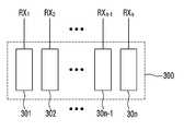
감지신호부(300)는 복수의 감지신호전극(RX1,RX2,…,RXn-1,RXn)에 인가되는 감지신호를 감지한다. 감지신호는 복수의 구동신호전극(TX1,TX2,…,TXn-1,TXn)과 복수의 감지신호전극(RX1,RX2,…,RXn-1,RXn)에 의해 생성되는 노드캐패시터(101)들의 캐패시턴스의 크기에 대한 정보를 포함할 수 있다. 그리고, 적어도 2개의 구동신호전극에 동시에 제1구동신호와 제2구동신호가 인가되면, 감지신호부(300)는 제1구간에서 생성된 감지신호들과 제2구간에서 생성된 감지신호를 연산하여 제1구동신호와 제2구동신호가 전달되는 노드캐패시터들 각각의 캐패시턴스를 파악할 수 있도록 할 수 있다. 따라서, 터치패널(100)의 복수의 노드 캐패시터들의 캐패시턴스를 동시에 인식할 수 있어 터치 패널(100)에서 복수 지점의 터치를 동시에 인식할 수 있다.The
일 실시예에 있어서, 제1구간과 제2구간에서 복수의 펄스의 수에 대응하여 감지신호를 수신하는 횟수를 결정하고, 수신된 감지신호들을 합산하여 노드캐패시터의 캐패시턴스에 대한 정보를 산출할 수 있다. 보다 구체적으로 설명하면, 구동신호의 복수의 펄스가 구동신호전극인 노드캐패시터의 일단에 전달되면, 노드캐패시터의 타단인 감지신호전극은 복수의 펄스에 대응하여 노드캐패시터의 타단의 전압변화를 감지할 수 있다. 그리고, 노드캐패시터의 타단의 전압변화를 합산하여 감지신호의 전압을 파악하고 이를 이용하여 노드캐패시터의 캐패시턴스를 파악할 수 있다. 이렇게 하면, 터치패널 입력장치(1000)의 노이즈가 분산되어 터치 패널(100)의 터치 감도를 향상시킬 수 있다.In one embodiment, the number of times of reception of the sensing signal corresponding to the number of pulses in the first section and the second section may be determined, and information about the capacitance of the node capacitor may be calculated by summing the received sensing signals have. More specifically, when a plurality of pulses of the driving signal are transmitted to one end of the node capacitor which is the driving signal electrode, the sensing signal electrode, which is the other end of the node capacitor, senses the voltage change of the other end of the node capacitor corresponding to the plurality of pulses . Then, the voltage change of the other end of the node capacitor is summed up so that the voltage of the sense signal can be grasped and the capacitance of the node capacitor can be grasped by using the voltage. By doing so, the noise of the touch
일 실시예에 있어서, 터치 패널 입력장치(1000)는 구동신호공급부(200)과 감지신호부(300)를 제어하여 구동신호공급부(200)에서 구동신호가 복수의 구동신호전극(TX1,TX2,…,TXn-1,TXn)에 인가되도록 하고, 복수의 감지신호전극(RX1,RX2,…,RXn-1,RXn)에 인가되는 감지신호를 감지신호부(300)에서 감지하도록 하는 제어부(400)를 더 포함할 수 있다. 또한, 터치패널 입력장치(1000)는 감지신호부(300)에서 제1구간과 제2구간에서 생성된 감지신호를 연산하지 않고 단순히 감지신호를 감지하고 제어부(400)에서 감지신호부(300)에서 감지한 감지신호를 전달받아 연산하여 제1구동신호와 제2구동신호가 전달되는 노드캐패시터들 각각의 캐패시턴스를 파악할 수 있도록 함으로써, 제어부(400)에서 터치 위치 정보를 생성할 수 있도록 할 수 있다.The touch
도 2는 도 1에 채용된 구동신호공급부의 구성을 나타내는 도면이다.2 is a diagram showing a configuration of a drive signal supply unit employed in FIG.
도 2를 참조하면, 구동신호공급부(200)는 복수의 구동블럭(201,202,…,20n-1.20n)을 포함하며, 각 구동블럭은 복수의 구동신호전극(TX1,TX2,…,TXn-1,TXn) 중 하나의 구동신호전극과 연결되고 구동신호전극에 구동신호를 공급할 수 있다. 또한, 복수의 구동블럭(201,202,…,20n-1.20n) 중 적어도 2개의 구동블럭이 동시에 구동신호를 서로 다른 적어도 2개의 구동신호전극에 공급할 수 있다. 일 실시형태에 있어서, 복수의 구동블럭(201,202,…,20n-1.20n)은 제어부(400)로부터 구동신호의 코드를 전달받아 구동신호를 생성할 수 있다. 구동신호의 코드는 하기의 도 3 내지 도 5에서 설명된다.2, the driving
도 3은 도 2에 도시된 구동신호공급부에서 생성되는 구동신호의 제1실시예를 나타내는 타이밍도이다.3 is a timing chart showing a first embodiment of a drive signal generated in the drive signal supply unit shown in FIG.
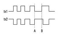
도 3을 참조하면, 구동신호공급부(200)에서 복수의 구동신호를 동시에 복수의 구동신호전극에 인가할 수 있지만 설명의 편의를 위해 제1구동신호 내지 제4구동신호(tx1 내지 tx4)가 동시에 제1내지 제4구동신호전극(TX1 내지 TX4)에 인가되는 것으로 가정하고 설명한다. 즉, 제1구동블럭(201) 내지 제4구동블럭(204)에서는 제1구동신호 내지 제4구동신호(tx1 내지 tx4)가 동시에 출력된다. 또한, 제1구동신호 내지 제4구동신호(tx1 내지 tx4)는 각각 제1구간 내지 제4구간(T1 내지 T4)으로 구분될 수 있다. 그리고, 제1구동신호 내지 제4구동신호(tx1 내지 tx4)는 각 구간에서 복수의 펄스를 포함할 수 있다. 복수의 펄스의 각 펄스폭은 달라 각 구간에서 복수의 펄스의 주파수가 일정하지 않을 수 있다. 그리고, 각 구간에서 구동신호의 코드는 복수의 펄스의 위상에 따라 1 또는 0으로 표현될 수 있다. 즉, 펄스가 동일 위상이면 1의 코드를 갖고 위상이 180도 차이이면 0의 코드를 갖도록 할 수 있다.Referring to FIG. 3, a plurality of driving signals can be simultaneously applied to a plurality of driving signal electrodes in the driving
제1구간(T1)에서 제1구동신호 내지 제4구동신호(tx1 내지 tx4)의 각 복수의 펄스는 동일한 위상으로 인가될 수 있다. 그리고, 제2구간(T2)에서 제1구동신호(tx1)와 제2구동신호(tx2)의 각 복수의 펄스는 제1구간(T1)에서와 동일한 위상으로 전달되고, 제3구동신호(tx3)와 제4구동신호(tx4)의 각 복수의 펄스는 제1구간(T1)에서와 위상이 180도 차이가 있도록 전달될 수 있다. 그리고, 제3구간(T3)에서 각 복수의 펄스는 제1구동신호(tx1)와 제4구동신호(tx4)는 제1구간(T1)에서와 동일한 위상으로 전달되고 제2구동신호(tx2)와 제3구동신호(tx3)의 각 복수의 펄스는 제1구간(T1)에서와 위상이 180도 차이가 있도록 전달될 수 있다. 그리고, 제4구간(T4)에서 제1구동신호(tx1)와 제3구동신호(tx3)의 각 복수의 펄스는 제1구간(T1)에서와 동일한 위상으로 전달되고 제2구동신호(tx2)와 제4구동신호(tx4)의 각 복수의 펄스는 제1구간(T1)에서와 위상이 180도 차이가 있도록 전달될 수 있다.In the first period T1, each of the plurality of pulses of the first to fourth driving signals tx1 to tx4 may be applied in the same phase. The plurality of pulses of the first driving signal tx1 and the second driving signal tx2 are transmitted in the same phase as in the first section T1 in the second section T2 and the third driving signal tx3 And the fourth driving signal tx4 may be transmitted so as to have a phase difference of 180 degrees from the first interval T1. The first driving signal tx1 and the fourth driving signal tx4 are transmitted in the same phase as in the first section T1 and the second driving signal tx2 is transmitted in the third section T3, And the third driving signal (tx3) may be transmitted so as to be 180 degrees out of phase with the first section (T1). The plurality of pulses of the first driving signal tx1 and the third driving signal tx3 are transmitted in the same phase as in the first period T1 and the second driving signal tx2 is transmitted in the fourth period T4, And the fourth driving signal (tx4) may be transmitted so as to have a phase difference of 180 degrees from the first interval (T1).
그리고, 제1구동신호(tx1)는 제1구간 내지 제4구간(T1 내지 T4)에서 위상의 변화가 없기 때문에 제1구간 내지 제4구간(T1 내지 T4)에서 제1구동신호(tx1)의 코드는 (1,1,1,1)이 될 수 있다. 그리고, 제2구동신호(tx2)는 제1구간(T1)과 제2구간(T2)에서는 위상 변화가 없지만 제3구간(T3)과 제4구간(T4)에서는 위상 변화가 있어 제1구간 내지 제4구간(T1 내지 T4)에서 제2구동신호(tx2)의 코드는 (1,1,0,0)이 될 수 있다. 그리고, 제3구동신호(tx3)는 제1구간(T1)과 제4구간(T4)에서는 위상 변화가 없지만 제2구간(T2)과 제3구간(T3)에서는 위상 변화가 있어 제1구간 내지 제4구간(T1 내지 T4)에서 제3구동신호(tx3)의 코드는 (1,0,0,1)이 될 수 있다. 또한, 제4구동신호(tx4)는 제1구간(T1)과 제3구간(T3)에서는 위상변화가 없지만 제2구간(T2)과 제4구간(T4)에서는 위상변화가 있어 제1구간 내지 제4구간(T1 내지 T4)에서 제4구동신호(tx4)의 코드는 (1,0,1,0)이 될 수 있다.Since the first driving signal tx1 has no phase change in the first to fourth periods T1 to T4, the first driving signal tx1 has the first driving signal tx1 in the first to fourth periods T1 to T4. The code can be (1,1,1,1). The second driving signal tx2 has no phase change in the first period T1 and the second period T2 but has a phase change in the third period T3 and the fourth period T4, The code of the second driving signal tx2 in the fourth period T1 to T4 may be (1, 1, 0, 0). The third driving signal tx3 has no phase change in the first period T1 and the fourth period T4 but has a phase change in the second period T2 and the third period T3, The code of the third driving signal tx3 in the fourth period T1 to T4 may be (1,0,0,1). The fourth driving signal tx4 has no phase change in the first period T1 and the third period T3 but has a phase change in the second period T2 and the fourth period T4, And the code of the fourth driving signal tx4 in the fourth period T1 to T4 may be (1, 0, 1, 0).
도 4는 도 2에 도시된 구동신호공급부에서 생성되는 구동신호의 제2실시예를 나타내는 타이밍도이다.4 is a timing chart showing a second embodiment of a drive signal generated in the drive signal supply unit shown in FIG.
도 4를 참조하면, 구동신호공급부(200)는 복수의 구동신호를 동시에 복수의 구동신호전극에 인가될 수 있지만 설명의 편의를 위해 제1구동신호 내지 제4구동신호(tx1 내지 tx4)가 동시에 제1구동신호전극 내지 제4구동신호전극(TX1 내지 TX4)에 인가되는 것으로 가정하고 설명한다. 즉, 제1구동블럭(201) 내지 제4구동블럭(204)에서는 제1구동신호 내지 제4구동신호(tx1 내지 tx4)가 동시에 출력된다. 그리고, 제1구동신호 내지 제4구동신호(tx1 내지 tx4)는 반복되는 각 하나의 구간에서 하이 상태 및/또는 로우 상태인 펄스를 포함할 수 있다. 그리고, 각 구간에서 구동신호의 코드는 펄스가 하이 상태 또는 로우 상태에 대응하여 구동신호의 펄스는 1 또는 0으로 표현될 수 있다. 복수의 펄스는 하이 상태 또는 로우 상태와 관계없이 복수의 펄스 중 적어도 2개의 펄스의 펄스폭이 다른 펄스들과 다를 수 있다.Referring to FIG. 4, the driving
제1구간(T1)에서 제1구동신호(tx1)는 하이 상태의 4개의 펄스를 포함할 수 있다. 4개의 펄스가 모두 하이 상태이므로, 제1구동신호(tx1)의 코드는 (1,1,1,1)이 될 수 있다. 그리고, 제2구동신호(tx2)는 하이 상태의 펄스와 로우 상태의 펄스를 포함하되, 먼저, 2개의 하이 상태의 펄스가 반복된 후 2개의 로우 상태의 펄스가 반복될 수 있다. 제2구동신호(tx2)는 하이 상태의 펄스가 반복된 후 로우 상태의 펄스가 반복되므로, 제2구동신호(tx2)의 코드는 (1,1,0,0)이 될 수 있다. 그리고, 제3구동신호(tx4)는 하이 상태의 펄스가 발생된 후 2개의 로우 상태의 펄스가 반복되고 다시 하이 상태의 펄스가 발생된다. 따라서, 제3구동신호(tx3)의 코드는 (1,0,0,1)이 될 수 있다. 그리고, 제4구동신호(tx4)는 하이 상태의 펄스와 로우 상태의 펄스가 반복될 수 있다. 제4구동신호(tx4)는 하이 상태의 펄스와 로우 상태의 펄스가 반복되므로, 제4구동신호(tx2)의 코드는 (1,0,0,1)이 될 수 있다.In the first period T1, the first driving signal tx1 may include four pulses in a high state. Since all four pulses are in the high state, the code of the first driving signal tx1 can be (1, 1, 1, 1). The second driving signal tx2 includes a high-state pulse and a low-state pulse. First, two low-state pulses may be repeated after the two high-state pulses are repeated. The pulse of the second driving signal tx2 may be (1, 1, 0, 0) since the pulse of the low state is repeated after the pulse of the high state is repeated. Then, the third driving signal (tx4) generates a high-state pulse, and then repeats the two low-state pulses and generates a high-state pulse again. Therefore, the code of the third driving signal tx3 may be (1, 0, 0, 1). The fourth drive signal tx4 can be repeated in the high state pulse and the low state pulse. Since the pulse of the high state and the pulse of the low state are repeated in the fourth drive signal tx4, the code of the fourth drive signal tx2 may be (1,0,0,1).
상기의 제1구간(T1)에서와 같은 제1구동신호 내지 제4구동신호(tx1 내지 tx4)가 제2구간 내지 제4구간(T2 내지 T4)에도 인가될 수 있다. 즉, 제1구간 내지 제4구간(T1 내지 T4)에서 1구동신호 내지 제4구동신호(tx1 내지 tx4)가 반복적으로 인가될 수 있다.The first to fourth driving signals tx1 to tx4 as in the first period T1 may be applied to the second period to the fourth period T2 to T4. That is, the first to fourth driving signals tx1 to tx4 may be repeatedly applied in the first to fourth periods T1 to T4.
또한, 펄스가 하이 상태이면 코드가 1로 설정되고 펄스가 로우 상태이면 0으로 설정된 것으로 설명되어 있으나 이에 한정되는 것은 아니다.In addition, if the pulse is high, the code is set to 1, and if the pulse is low, it is set to zero. However, the present invention is not limited thereto.
도 5는 도 2에 도시된 구동신호공급부에서 생성되는 구동신호의 제3실시예를 나타내는 타이밍도이다.5 is a timing chart showing a third embodiment of a drive signal generated by the drive signal supply unit shown in FIG.
도 5를 참조하면, 구동신호공급부(200)는 복수의 구동신호를 동시에 복수의 구동신호전극에 인가될 수 있지만 설명의 편의를 위해 제1구동신호 내지 제16구동신호(tx1 내지 tx16)가 동시에 제1내지 제16구동신호전극(TX1 내지 TX16)에 인가되는 것으로 가정하고 설명한다. 즉, 제1구동블럭(201) 내지 제16구동블럭(216)에서는 제1구동신호 내지 제16구동신호(tx1 내지 tx16)가 동시에 출력된다. 또한, 제1구동신호 내지 제16구동신호(tx1 내지 tx16)는 제1구간 내지 제4구간(T1 내지 T4)의 4개의 구간으로 구분될 수 있다. 그리고, 제1구동신호 내지 제16구동신호(tx1 내지 tx16)는 반복되는 각 구간에서 복수의 펄스를 포함할 수 있다. 그리고, 복수의 펄스는 제1구동신호 내지 제16구동신호(tx1 내지 tx16)는 반복되는 각 하나의 구간에서 하이 상태 및/또는 로우 상태인 펄스를 포함할 수 있다. 그리고, 복수의 펄스는 적어도 2개의 펄스폭이 다른 펄스들과 다를 수 있다. 그리고, 각 구간에서 구동신호의 코드는 펄스의 하이 상태 또는 로우 상태와 펄스의 위상에 대응하여 구동신호의 펄스는 1 또는 0으로 표현될 수 있다. 즉, 각 구간에서 위상 변화가 없다면 하이 상태의 펄스에 의해 코드는 1로 결정되고 로우 상태의 코드는 0으로 결정될 수 있지만, 위상 변화가 있으면 하이 상태의 코드는 0으로 결정되고 로우 상태의 코드는 1로 결정될 수 있다.Referring to FIG. 5, the driving
제1구동신호 내지 제4구동신호(tx1 내지 tx4)는 제1구간 내지 제4구간(T1 내지 T4)에서 모두 하이 상태인 복수의 펄스를 포함할 수 있다. 그리고, 제1구동신호(tx1)는 제1구간 내지 제4구간(T1 내지 T4)에서 위상의 변화가 없다. 따라서, 제1구동신호(tx1)의 코드는 제1구간 내지 제4구간(T1 내지 T4)에서 (1,1,1,1,1,1,1,1,1,1,1,1,1,1,1,1)이 될 수 있다. 그리고, 제2구동신호(tx2)는 제1구간(T1)과 제2구간(T2)에서는 위상 변화가 없지만 제3구간(T3)과 제4구간(T4)에서는 위상 변화가 있다. 따라서, 제2구동신호(tx2)의 코드는 제1구간 내지 제4구간(T1 내지 T4)에서 (1,1,1,1,1,1,1,1,0,0,0,0,0,0,0,0)이 될 수 있다. 그리고, 제3구동신호(tx3)는 제1구간(T1)과 제4구간(T4)에서는 위상 변화가 없고 제2구간(T2)과 제3구간(T4)에서는 위상 변화가 있어 제1구간 내지 제4구간(T1 내지 T4)에서 제3구동신호(tx3)의 코드는 (1,1,1,1,0,0,0,0,0,0,0,0,1,1,1,1)이 될 수 있다. 또한, 제4구동신호(tx4)는 제1구간(T1)과 제3구간(T3)에서는 위상변화가 없지만 제2구간(T2)과 제4구간(T4)에서는 위상변화가 있어 제1구간 내지 제4구간(T1 내지 T4)에서 제4구동신호(tx4)의 코드는 (1,1,1,1.0.0.0.0, 1,1,1,1.0.0.0.0)이 될 수 있다.The first to fourth driving signals tx1 to tx4 may include a plurality of pulses that are both high in the first to fourth periods T1 to T4. The first driving signal tx1 has no phase change in the first to fourth periods T1 to T4. Therefore, the code of the first driving signal tx1 is (1, 1, 1, 1, 1, 1, 1, 1, 1, 1, 1, 1, 1, 1, 1, 1). The second driving signal tx2 has no phase change in the first section T1 and the second section T2 but has a phase change in the third section T3 and the fourth section T4. Therefore, the code of the second driving signal tx2 is (1, 1, 1, 1, 1, 1, 1, 0, 0,0,0,0). The third driving signal tx3 has no phase change in the first period T1 and the fourth period T4 and has a phase change in the second period T2 and the third period T4. In the fourth period T1 to T4, the code of the third driving signal tx3 is (1,1,1,1,0,0,0,0,0,0,0,0,1,1,1,1, 1). The fourth driving signal tx4 has no phase change in the first period T1 and the third period T3 but has a phase change in the second period T2 and the fourth period T4, The code of the fourth driving signal tx4 in the fourth period T1 to T4 may be (1,1,1, 1.0.0.0.0, 1,1,1, 1.0.0.0.0).
제5구동신호 내지 제8구동신호(tx5 내지 tx8)는 제1구간 내지 제4구간(T1 내지 T4)에서 2개의 하이 상태의 펄스와 2개의 로우 상태의 펄스를 포함할 수 있다. 그리고, 2개의 하이 상태의 펄스가 발생된 후 2개의 로우 상태의 펄스가 발생될 수 있다. 그리고, 제5구동신호(tx5)는 제1구간 내지 제4구간(T1 내지 T4)에서 위상의 변화가 없다. 따라서, 제5구동신호(tx5)의 코드는 제1구간 내지 제4구간(T1 내지 T4)에서 (1,1,0,0,1,1,0,0,1,1,0,0,1,1,0,0)이 될 수 있다. 그리고, 제6구동신호(tx6)는 제1구간(T1)과 제2구간(T2)에서는 위상 변화가 없지만 제3구간(T3)과 제4구간(T4)에서는 위상 변화가 있을 수 있다. 따라서, 제6구동신호(tx6)의 코드는 제1구간 내지 제4구간(T1 내지 T4)에서 (1,1,0,0,1,1,0,0,0,0,1,1,0,0,1,1)이 될 수 있다. 그리고, 제7구동신호(tx7)는 제1구간(T1)과 제4구간(T4)에서는 위상 변화가 없고 제2구간(T2)과 제3구간(T4)에서는 위상 변화가 있어 제1구간 내지 제4구간(T1 내지 T4)에서 제7구동신호(tx7)의 코드는 (1,1,0,0,0,0,1,1,0,0,1,1,1,1,0,0)이 될 수 있다. 또한, 제8구동신호(tx8)는 제1구간(T1)과 제3구간(T3)에서는 위상변화가 없지만 제2구간(T2)과 제4구간(T4)에서는 위상변화가 있어 제1구간 내지 제4구간(T1 내지 T4)에서 제8구동신호(tx8)의 코드는 (1,1,0,0,0,0,1,1,1,1,0,0,0,0,1,1)이 될 수 있다.The fifth to eighth driving signals tx5 to tx8 may include two high-state pulses and two low-state pulses in the first to fourth periods T1 to T4. After two high-state pulses are generated, two low-state pulses may be generated. The fifth driving signal tx5 has no phase change in the first to fourth periods T1 to T4. Accordingly, the code of the fifth driving signal tx5 is (1, 1, 0, 0, 1, 1, 0, 0, 1, 1, 0, 0). The sixth driving signal tx6 has no phase change in the first period T1 and the second period T2 but may have a phase change in the third period T3 and the fourth period T4. Therefore, the code of the sixth driving signal tx6 is (1, 1, 0, 0, 1, 1, 0, 0, 0, 0, 1, 1). The seventh driving signal tx7 has no phase change in the first section T1 and the fourth section T4 and has a phase change in the second section T2 and the third section T4. In the fourth period T1 to T4, the code of the seventh drive signal tx7 is (1,1,0,0,0,0,1,1,0,0,1,1,1,1,0, 0). The eighth driving signal tx8 has no phase change in the first section T1 and the third section T3 but has a phase change in the second section T2 and the fourth section T4, In the fourth period T1 to T4, the code of the eighth drive signal tx8 is (1,1,0,0,0,0,1,1,1,1,0,0,0,0,1, 1).
제9구동신호 내지 제12구동신호(tx9 내지 tx12)는 제1구간 내지 제4구간(T1 내지 T4)에서 2개의 하이 상태의 펄스와 2개의 로우 상태의 펄스를 포함할 수 있다. 그리고, 2개의 하이 상태의 펄스 사이에 2개의 로우 상태의 펄스가 발생될 수 있다. 그리고, 제9구동신호(tx9)는 제1구간 내지 제4구간(T1 내지 T4)에서 위상의 변화가 없다. 따라서, 제9구동신호(tx9)의 코드는 제1구간 내지 제4구간(T1 내지 T4)에서 (1,0,0,1,1,0,0,1,1,0,0,1,1,0,0,1)이 될 수 있다. 그리고, 제10구동신호(tx10)는 제1구간(T1)과 제2구간(T2)에서는 위상 변화가 없지만 제3구간(T3)과 제4구간(T4)에서는 위상 변화가 있다. 따라서, 제10구동신호(tx10)의 코드는 제1구간 내지 제4구간(T1 내지 T4)에서 (1,0,0,1,1,0,0,1,0,1,1,0,0,1,1,0)이 될 수 있다. 그리고, 제11구동신호(tx11)는 제1구간(T1)과 제4구간(T4)에서는 위상 변화가 없고 제2구간(T2)과 제3구간(T4)에서는 위상 변화가 있어 제1구간 내지 제4구간(T1 내지 T4)에서 제11구동신호(tx11)의 코드는 (1,0,0,1,0,1,1,0,0,1,1,0,1,0,0,1) 이 될 수 있다. 또한, 제12구동신호(tx12)는 제1구간(T1)과 제3구간(T3)에서는 위상변화가 없지만 제2구간(T2)과 제4구간(T4)에서는 위상변화가 있어 제1구간 내지 제4구간(T1 내지 T4)에서 제12구동신호(tx12)의 코드는 (1,0,0,1,0,1,1,0,0,1,1,0,1,0,0,1) 이 될 수 있다.The ninth driving signal to the twelfth driving signal tx9 to tx12 may include two high state pulses and two low state pulses in the first to fourth periods T1 to T4. Then, two low-state pulses may be generated between the two high-state pulses. The ninth driving signal tx9 has no phase change in the first to fourth periods T1 to T4. Therefore, the code of the ninth driving signal tx9 is (1, 0, 0, 1, 1, 0, 0, 1, 1, 0, 0, 1). The tenth driving signal tx10 has no phase change in the first section T1 and the second section T2 but has a phase change in the third section T3 and the fourth section T4. Therefore, the code of the tenth driving signal tx10 is (1, 0, 0, 1, 1, 0, 1, 0, 1, 1, 0,1,1,0). The eleventh driving signal tx11 has no phase change in the first section T1 and the fourth section T4 and has a phase change in the second section T2 and the third section T4. In the fourth period T1 to T4, the code of the eleventh driving signal tx11 is (1,0,0,1,0,1,1,0,0,1,1,1,0,1,0,0, 1). The twelfth driving signal tx12 has no phase change in the first section T1 and the third section T3 but has a phase change in the second section T2 and the fourth section T4, In the fourth period T1 to T4, the code of the twelfth driving signal tx12 is (1,0,0,1,0,1,1,0,0,1,1,1,0,1,0,0, 1).
제13구동신호 내지 제16구동신호(tx13 내지 tx16)는 제1구간 내지 제4구간(T1 내지 T4)에서 교번적으로 발생하는 하이 상태의 펄스와 로우 상태의 펄스를 포함할 수 있다. 그리고, 제13구동신호(tx13)는 제1구간 내지 제4구간(T1 내지 T4)에서 위상의 변화가 없다. 따라서, 제13구동신호(tx13)의 코드는 제1구간 내지 제4구간(T1 내지 T4)에서 (1,0,1,0,1,0,1,0,1,0,1,0,1,0,1,0)이 될 수 있다. 그리고, 제14구동신호(tx14)는 제1구간(T1)과 제2구간(T2)에서는 위상 변화가 없지만 제3구간(T3)과 제4구간(T4)에서는 위상 변화가 있다. 따라서, 제14구동신호(tx14)의 코드는 제1구간 내지 제4구간(T1 내지 T4)에서 (1,0,1,0,1,0,1,0,0,1,0,1,0,1,0,1)이 될 수 있다. 그리고, 제15구동신호(tx15)는 제1구간(T1)과 제4구간(T4)에서는 위상 변화가 없고 제2구간(T2)과 제3구간(T4)에서는 위상 변화가 있어 제1구간 내지 제4구간(T1 내지 T4)에서 제15구동신호(tx15)의 코드는 (1,0,1,0,0,1,0,1,0,1,0,1,1,0,1,0)이 될 수 있다. 또한, 제16구동신호(tx16)는 제1구간(T1)과 제3구간(T3)에서는 위상변화가 없지만 제2구간(T2)과 제4구간(T4)에서는 위상변화가 있어 제1구간 내지 제4구간(T1 내지 T4)에서 제16구동신호(tx16)의 코드는 (1,0,1,0,0,1,0,1,1,0,1,0,0,1,0,1)이 될 수 있다.The thirteenth to sixteenth driving signals tx13 to tx16 may include a high-state pulse and a low-state pulse alternately generated in the first to fourth periods T1 to T4. The thirteenth driving signal tx13 has no phase change in the first to fourth periods T1 to T4. Therefore, the code of the thirteenth driving signal tx13 is (1, 0, 1, 0, 1, 0, 1, 0, 1, 1, 0, 1, 0). The fourteenth driving signal tx14 has no phase change in the first section T1 and the second section T2 but has a phase change in the third section T3 and the fourth section T4. Therefore, the code of the fourteenth driving signal tx14 is (1, 0, 1, 0, 1, 0, 1, 0, 0, 1, 0, 1). The fifteenth driving signal tx15 has no phase change in the first section T1 and the fourth section T4 and has a phase change in the second section T2 and the third section T4. In the fourth period T1 to T4, the code of the fifteenth driving signal tx15 is (1, 0, 1, 0, 0, 1, 0, 1, 0). The 16th driving signal tx16 has no phase change in the first section T1 and the third section T3 but has a phase change in the second section T2 and the fourth section T4, In the fourth period T1 to T4, the code of the sixteenth driving signal tx16 is (1, 0, 1, 0, 0, 1, 0, 1, 1).
도 6은 도 3에 도시된 구동신호의 파형의 다른 일실시예를 나타내는 타이밍도이다.6 is a timing chart showing another embodiment of the waveform of the drive signal shown in Fig.
도 6을 참조하면, 구동신호공급부(200)에서 적어도 2개의 구동신호전극에 동시에 인가하는 제1구동신호(tx1)와 제2구동신호(tx2)는 위상이 180도 차이를 갖는다.Referring to FIG. 6, the first driving signal tx1 and the second driving signal tx2, which are simultaneously applied to at least two driving signal electrodes in the driving
제1구동신호(tx1)와 제2구동신호(tx2)는 펄스폭이 일정하지 않아 주기적인 펄스신호가 아닐 수 있다. 일례로 제1구동신호(tx1)와 제2구동신호(tx2)는 복수의 펄스의 주기가 동일하지 않은 스프레드 스펙트럼 펄스(Spread Spectrum Pulse)일 수 있다. 또한, A 지점에서 제1구동신호(tx1)의 폴링에지(falling edge)와 제2구동신호(tx2)의 라이징에지(rising edge)는 동시에 발생되지만 B지점에서 제1구동신호(tx1)의 라이징에지는 발생되지만 제2구동신호(tx2)의 폴링에지는 B 지점 후에 발생된다. 즉, 펄스의 하이 구간과 로우 구간의 비인 듀티비(duty ratio)가 제1구동신호(tx1)와 제2구동신호(tx2)는 다를 수 있다. 따라서, 제1구동신호(tx1)와 제2구동신호(tx2)의 주파수가 일치하지 않게 될 수 있다.The first driving signal tx1 and the second driving signal tx2 may not be a periodic pulse signal because the pulse width is not constant. For example, the first driving signal tx1 and the second driving signal tx2 may be a spread spectrum pulse having a plurality of pulses whose periods are not the same. The falling edge of the first driving signal tx1 at the point A and the rising edge of the second driving signal tx2 are simultaneously generated but the rising edge of the first driving signal tx1 at the point B The edge of the second driving signal tx2 is generated but the polling edge of the second driving signal tx2 is generated after the point B. That is, the first driving signal tx1 and the second driving signal tx2 may be different from each other in the duty ratio, which is the ratio between the high and low pulse intervals. Therefore, the frequencies of the first driving signal tx1 and the second driving signal tx2 may become inconsistent.
상기의 설명에서는 도 3의 2개의 구동신호에 대해 듀티비가 일정하지 않은 것을 설명하고 있지만, 이에 한정되는 것은 아니고 도 4 또는 도 5에 도시된 구동신호 역시 위상이 다른 경우 듀티비가 일정하지 않을 수 있다.In the above description, the duty ratio is not constant for the two drive signals in FIG. 3. However, the present invention is not limited to this. The drive signals shown in FIG. 4 or 5 may have different duty ratios in different phases .
도 7은 도 1에 채용된 감지신호부의 구성을 나타내는 도면이다.FIG. 7 is a diagram showing a configuration of a sense signal unit employed in FIG. 1. FIG.
도 7을 참조하면, 감지신호부(300)는 복수의 감지신호검출부(301,302,…,30n-1,30n)를 포함하며, 각 감지신호검출부 (301,302,…,30n-1,30n)는 각각 하나의 감지신호전극(RX1,RX2,…,RXn-1,RXn)과 연결될 수 있다. 복수의 감지신호검출부(301,302,…,30n-1,30n)는 각각 동일한 구성을 할 수 있어, 여기서는 제1감지전극(RX1)과 연결되어 있는 제1감지신호검출부(301)에서의 동작만을 설명한다.7, the
제1구간(T1)에서 제1구동신호전극 내지 제4구동신호전극(TX1 내지 TX4)로 동시에 전달되는 제1구동신호 내지 제4구동신호(tx1 내지 tx4)는 위상이 갖은 동일한 파형을 갖는 신호이므로, 제1구동신호 내지 제4구동신호(tx1 내지 tx4)는 (+)부호와 동일한 크기의 전압을 갖는 것으로 판단할 수 있다. 따라서, 제1감지신호검출부(301)는 제1감지전극(RX1)으로부터 하기의 수학식 2와 같은 전압을 검출할 수 있다.The first driving signal to the fourth driving signal tx1 to tx4 simultaneously transmitted from the first driving signal electrode to the fourth driving signal electrode TX1 to TX4 in the first period T1 have the same waveform , It can be determined that the first to fourth driving signals tx1 to tx4 have the same magnitude as the (+) sign. Therefore, the first sensing

그리고, 제2구간(T2)에서 제1구동신호전극 내지 제4구동신호전극(TX1 내지 TX4)로 동시에 전달되는 제1구동신호 내지 제4구동신호(tx1 내지 tx4) 중 제1구동신호(tx1)와 제2구동신호(tx2)는 위상이 동일하지만 제3구동신호(tx3)와 제4구동신호(tx4)는 위상이 다르기 때문에 제1구동신호와 제2구동신호는 (+) 부호와 동일한 크기의 전압으로 판단할 수 있고 제3구동신호(tx3)와 제4구동신호(tx4)는 동일한 크기를 갖지만 (-) 부호를 갖는 전압으로 판단할 수 있다. 따라서, 제1감지신호검출부(301)는 제1감지전극(RX1)으로부터 하기의 수학식 3과 같은 전압을 검출할 수 있다.Of the first drive signal to the fourth drive signal tx1 to tx4 simultaneously transmitted from the first drive signal electrode to the fourth drive signal electrode TX1 to TX4 in the second period T2, the first drive signal tx1 ) And the second driving signal tx2 are in phase but the third driving signal tx3 and the fourth driving signal tx4 are in phase different from each other so that the first driving signal and the second driving signal have the same And the third drive signal tx3 and the fourth drive signal tx4 have the same magnitude but can be determined as a voltage having a minus sign. Therefore, the first

VRX12= (C11+ C12- C13- C14)× AVTXVRX12 = (C11 + C12 - C13 - C14) x AVTX
그리고, 제3구간(T3)에서 제1구동신호전극 내지 제4구동신호전극(TX1 내지 TX4)로 동시에 전달되는 제1구동신호 내지 제4구동신호(tx1 내지 tx4) 중 제1구동신호(tx1)와 제4구동신호(tx4)는 위상이 동일하지만 제2구동신호(tx2)와 제3구동신호(tx3)는 위상이 다르기 때문에 제1구동신호(tx1)와 제4구동신호(tx4)는 (+) 부호와 동일한 크기의 전압으로 판단할 수 있고 제2구동신호(tx2)와 제3구동신호(tx3)는 동일한 크기를 갖지만 (-) 부호를 갖는 전압으로 판단할 수 있다. 따라서, 제1감지신호검출부(301)는 제1감지전극(RX1)으로부터 하기의 수학식 4와 같은 전압을 검출할 수 있다.Of the first to fourth driving signals tx1 to tx4 simultaneously transmitted from the first driving signal electrode to the fourth driving signal electrode TX1 to TX4 in the third period T3, the first driving signal tx1 The fourth driving signal tx4 and the fourth driving signal tx4 are in phase but the second driving signal tx2 and the third driving signal tx3 have different phases, The second driving signal tx2 and the third driving signal tx3 have the same magnitude but can be determined as a voltage having a minus sign. Therefore, the first sensing

그리고, 제4구간(T4)에서 제1구동신호전극 내지 제4구동신호전극(TX1 내지 TX4)로 동시에 전달되는 제1구동신호 내지 제4구동신호(tx1 내지 tx4) 중 제1구동신호(tx1)와 제3구동신호(tx3)는 위상이 동일하지만 제2구동신호(tx2)와 제4구동신호(tx4)는 위상이 다르기 때문에 제1구동신호(tx1)와 제3구동신호(tx3)는 (+) 부호와 동일한 크기의 전압으로 판단할 수 있고 제2구동신호(tx2)와 제4구동신호(tx4)는 동일한 크기를 갖지만 (-) 부호를 갖는 전압으로 판단할 수 있다. 따라서, 제1감지신호검출부(301)는 제1감지전극(RX1)으로부터 하기의 수학식 5와 같은 전압을 검출할 수 있다.Of the first to fourth driving signals tx1 to tx4 simultaneously transmitted from the first driving signal electrode to the fourth driving signal electrode TX1 to TX4 in the fourth period T4, the first driving signal tx1 The third driving signal tx3 and the third driving signal tx3 have the same phase but the second driving signal tx2 and the fourth driving signal tx4 have different phases, The second driving signal tx2 and the fourth driving signal tx4 have the same magnitude but can be determined as a voltage having a minus sign. Therefore, the first

상기의 수학식 1 내지 4에서 VRX11 내지 VRX14는 제1구간 내지 제4구간(T1 내지 T4)에서 제1감지신호검출부(301)에서 제1감지전극(RX1)으로부터 검출된 감지신호의 전압, C11 내지 C14는 제1감지전극과 연결된 노드캐패시터들, VTX은 제1구동신호전극을 통해 인가되는 구동신호의 전압, A는 상수를 의미할 수 있다.In the
그리고, 상기의 수학식 2 내지 수학식 5를 행렬식으로 표시하면, 하기의 수학식 6와 같게 된다.The mathematical expressions (2) to (5) can be expressed by the following mathematical expression (6).

그리고, 상기의 수학식 5의 역행렬을 이용하여 각 노드캐패시터들의 캐패시턴스를 파악할 수 있다.The capacitance of each node capacitor can be determined using the inverse matrix of Equation (5).
상기 수학식 6의 역행렬은 하기의 수학식 7과 같게 된다.The inverse matrix of Equation (6) becomes Equation (7).

따라서, 동시에 4개의 노드캐패시터의 캐패시턴스를 파악할 수 있다.Therefore, the capacitances of the four node capacitors can be grasped at the same time.
상기의 설명은 4개의 노드캐패시터들의 캐패시턴스를 파악하는 것으로 설명되어 있지만, 이에 한정되는 것은 아니며 도 5에 도시되어 있는 것과 같이 16개의 구동신호 전극에 동시에 서로 다른 구동신호를 인가하고 제1구간 내지 제4구간(T1 내지 T4) 동안 감지신호를 분석함으로써 16개의 노드캐패시터들의 캐패시턴스를 판단할 수도 있다.However, the present invention is not limited to this. It is also possible to apply different driving signals to 16 driving signal electrodes at the same time as shown in FIG. 5, The capacitance of the sixteen node capacitors may be determined by analyzing the sensing signal during the four periods T1 to T4.
또한, 제1감지신호검출부(301)는 구동신호의 복수의 펄스의 수에 대응하여 노드캐패시터의 캐패시턴스를 감지하는 횟수를 결정할 수 있다. 즉, 제1구간 내지 제4구간(T1 내지 T4)의 각 구간에서 구동신호들의 복수의 펄스의 수가 4개이면, 감지신호검출부(301)는 제1구간(T1) 내지 제4구간(T5)에서 각각 4번의 감지신호를 센싱하고 센싱한 결과를 합산하여 상기의 수학식 5를 산출할 수 있다. 이렇게 합산을 하게 되면, 노이즈가 각 펄스 별로 분산되어 있기 때문에 터치 패널 입력장치(1000)가 노이즈의 영향을 적게 받을 수 있어서, 터치 패널(100)의 터치의 인식을 정확히 하여 터치 감도를 향상시킬 수 있다.Also, the first
도 8은 도 1에 도시된 터치 패널에서 입력을 검출하는 방법을 나타내는 순서도이다.8 is a flowchart showing a method of detecting an input in the touch panel shown in Fig.
도 8을 참조하면, 복수의 노드캐패시터를 포함하며, 각 노드캐패시터는 복수의 구동신호전극 중 하나의 구동신호전극과, 복수의 감지신호전극 중 하나의 감지신호전극에 의해 형성되는 터치 패널의 입력검출은, 복수의 펄스 중 적어도 하나의 펄스는 폭이 다른 펄스의 폭과 다르고, 제2구동신호의 복수의 펄스 중 적어도 하나의 펄스는 제1구간과 제2구간 중 하나의 구간에서 제1구동신호의 복수의 펄스와 위상이 다르게 인가될 수 있다.(S800) 이때, 제1구동신호와 제2구동신호는 제1구간과 제2구간에서 각각 복수의 펄스를 포함하고, 제1구간과 제2구간 중 하나의 구간에서 제2구동신호의 펄스는 제1구동신호의 펄스와 다르게 인가된다. 여기서, 다르게 인가된다는 것은 제2구동신호의 펄스는 제1구동신호의 펄스와 위상이 다른 것을 포함할 수 있다. 또한, 복수의 펄스는 하이 상태와 로우 상태가 반복되고, 제1구동신호의 펄스가 반복되는 순서와 제2구동신호의 펄스가 반복되는 순서와 다르게 인가되는 것을 포함할 수 있다. 또한, 제1구동신호와 제2구동신호의 각각의 복수의 펄스는 하이 상태와 로우 상태가 반복될 수 있고, 제1구동신호의 펄스가 반복되는 순서와 제2구동신호의 펄스가 반복되는 순서는 다르게 설정될 수 있다.8, each of the node capacitors includes a driving signal electrode of a plurality of driving signal electrodes, an input of a touch panel formed by one of the plurality of sensing signal electrodes, Wherein at least one of the plurality of pulses is different from a width of a pulse having a different width and at least one pulse of the plurality of pulses of the second driving signal is pulsed in one of a first period and a second period, (S800). At this time, the first driving signal and the second driving signal include a plurality of pulses in the first period and the second period, respectively, and the first period and the second period are different from each other in the first period and the second period. The pulse of the second driving signal is applied differently from the pulse of the first driving signal in one of the two periods. Herein, the pulses of the second driving signal may be different in phase from the pulses of the first driving signal. Also, the plurality of pulses may include a high state and a low state being repeated and being applied differently from the order in which the pulses of the first driving signal are repeated and the order in which the pulses of the second driving signal are repeated. The plurality of pulses of the first driving signal and the second driving signal may be repeated in a high state and a low state, and the order of repeating the pulses of the first driving signal and the order of repeating the pulses of the second driving signal Can be set differently.
그리고, 제1구간과 제2구간에서 복수의 감지신호전극으로부터 복수의 노드캐패시터 중 적어도 2개의 노드캐패시터의 캐패시턴스에 대한 정보를 포함하는 감지신호들을 감지신호검출부에서 수신할 수 있다.(S810) 적어도 2개의 노드 캐패시터의 캐패시턴스를 동시에 인식하게 되면 터치 패널(100)에서 복수 지점의 터치를 동시에 인식할 수 있다. 일 실시예에 있어서, 감지신호검출부는 제1구간과 제2구간에서 복수의 펄스의 수에 대응하여 상기 감지신호를 수신하는 횟수를 결정하고, 수신된 감지신호들을 합산하여 노드캐패시터의 캐패시턴스에 대한 정보를 산출할 수 있다. 즉, 복수의 펄스의 수가 4개이면, 한 구간에서 감지신호를 4번 검출하고, 검출된 감지신호를 합산하여 노드캐패시터의 캐패시턴스를 파악할 수 있다. 이렇게 여러 번 감지신호를 검출하게 되면, 노이즈가 분산되게 되고 이로 인해, 노드캐패시터의 캐패시턴스에 대한 정보가 노이즈의 영향을 적게 받도록 할 수 있고 터치 패널의 터치 감도를 향상시킬 수 있다.The sensing signal detecting unit may receive sensing signals including information on the capacitances of at least two of the plurality of node capacitors from the plurality of sensing signal electrodes in the first section and the second section in operation S810. When the capacitances of the two node capacitors are recognized at the same time, the
그리고, 감지신호검출부에서 적어도 2개의 노드캐패시터의 캐패시턴스에 대한 정보를 이용하여 터치 패널의 터치 정보를 추출할 수 있다.(S820) 여기서, 터치 패널의 터치 정보를 감지신호검출부에서 추출하는 것으로 설명하였지만, 이에 한정되는 것은 아니며, 감지신호검출부에서 검출한 노드캐패시터의 캐패시턴스에 대한 정보를 제어부에 전달하고 제어부에서 연산을 하여 터치 패널의 터치 정보를 추출할 수 있다.In addition, it is possible to extract the touch information of the touch panel using the information about the capacitances of at least two node capacitors in the detection signal detection unit (S820). Here, the touch information detection unit of the touch panel extracts the touch information However, the present invention is not limited thereto, and information about the capacitance of the node capacitor detected by the sensing signal detector may be transmitted to the controller, and the controller may extract the touch information of the touch panel.
이상에서 실시예들에 설명된 특징, 구조, 효과 등은 본 발명의 적어도 하나의 실시예에 포함되며, 반드시 하나의 실시예에만 한정되는 것은 아니다. 나아가, 각 실시예에서 예시된 특징, 구조, 효과 등은 실시예들이 속하는 분야의 통상의 지식을 가지는 자에 의해 다른 실시예들에 대해서도 조합 또는 변형되어 실시 가능하다. 따라서 이러한 조합과 변형에 관계된 내용들은 본 발명의 범위에 포함되는 것으로 해석되어야 할 것이다.The features, structures, effects and the like described in the embodiments are included in at least one embodiment of the present invention and are not necessarily limited to only one embodiment. Furthermore, the features, structures, effects and the like illustrated in the embodiments can be combined and modified by other persons skilled in the art to which the embodiments belong. Therefore, it should be understood that the present invention is not limited to these combinations and modifications.
또한, 이상에서 실시예를 중심으로 설명하였으나 이는 단지 예시일 뿐 본 발명을 한정하는 것이 아니며, 본 발명이 속하는 분야의 통상의 지식을 가진 자라면 본 실시예의 본질적인 특성을 벗어나지 않는 범위에서 이상에 예시되지 않은 여러 가지의 변형과 응용이 가능함을 알 수 있을 것이다. 예를 들어, 실시예에 구체적으로 나타난 각 구성 요소는 변형하여 실시할 수 있는 것이다. 그리고 이러한 변형과 응용에 관계된 차이점들은 첨부된 청구 범위에서 규정하는 본 발명의 범위에 포함되는 것으로 해석되어야 할 것이다.While the present invention has been particularly shown and described with reference to exemplary embodiments thereof, it is clearly understood that the same is by way of illustration and example only and is not to be taken by way of illustration, It can be seen that various modifications and applications are possible. For example, each component specifically shown in the embodiments can be modified and implemented. It is to be understood that all changes and modifications that come within the meaning and range of equivalency of the claims are therefore intended to be embraced therein.
100:터치패널101: 노드캐패시터
200:구동신호공급부300:감지신호부
TX1,TX2,…,TXn-1,TXn: 구동신호전극
RX1,RX2,…,RXn-1,RXn: 감지신호전극
400: 제어부500: 디스플레이부
1000: 터치 패널 입력장치100: touch panel 101: node capacitor
200: driving signal supply unit 300: sensing signal unit
TX1, TX2, ... , TXn-1, TXn: driving signal electrode
RX1, RX2, ... , RXn-1, RXn: sensing signal electrode
400: control unit 500: display unit
1000: Touch panel input device
Claims (13)
Translated fromKorean상기 복수의 구동신호전극 중 적어도 2개의 구동신호전극에 각각 제1구동신호와 제2구동신호를 동시에 인가하되, 제1구간과 제2구간에서 상기 제1구동신호와 상기 제2구동신호는 각각 복수의 펄스를 포함하고, 상기 복수의 펄스 중 적어도 하나의 펄스의 폭은 다른 펄스의 폭과 다르고, 상기 제2구동신호의 복수의 펄스 중 적어도 하나의 펄스는 상기 제1구간과 상기 제2구간 중 하나의 구간에서 상기 제1구동신호의 복수의 펄스와 위상이 다른 구동신호공급부; 및
상기 제1구간과 상기 제2구간에서 상기 복수의 감지신호전극으로부터의 상기 복수의 노드캐패시터 중 적어도 2개의 노드캐패시터의 캐패시턴스에 대한 정보를 포함하는 감지신호들을 수신하는 감지신호부를 포함하는 터치 패널 입력장치.A plurality of node capacitors, each of the node capacitors being formed by one of a plurality of driving signal electrodes and a plurality of sensing signal electrodes;
A first driving signal and a second driving signal are simultaneously applied to at least two driving signal electrodes of the plurality of driving signal electrodes, and in the first and second sections, the first driving signal and the second driving signal are respectively Wherein a width of at least one of the plurality of pulses is different from a width of the other pulses and at least one of a plurality of pulses of the second driving signal is divided into a first period and a second period, A driving signal supply unit having a phase different from that of the plurality of pulses of the first driving signal; And
And a sensing signal unit for receiving sensing signals including information on capacitances of at least two of the plurality of node capacitors from the plurality of sensing signal electrodes in the first section and the second section, Device.
상기 복수의 펄스 중 적어도 하나의 펄스는 하이 상태이고 또 다른 하나의 펄스는 로우 상태인 터치 패널 입력장치.The method according to claim 1,
Wherein at least one of the plurality of pulses is high and the other pulse is low.
상기 하이 상태와 상기 로우 상태는 펄스폭이 다른 터치 패널 입력장치.3. The method of claim 2,
Wherein the high state and the low state have different pulse widths.
상기 하이 상태와 상기 로우 상태가 교번적으로 나타나는 터치 패널 입력장치.The method according to claim 2 or 3,
Wherein the high state and the low state alternately appear.
상기 제2구간에서 상기 제1구동신호의 복수의 펄스 중 적어도 하나의 펄스의 듀티비는 상기 제2구동신호의 복수의 펄스 중 적어도 하나의 펄스의 듀티비와 다른 터치 패널 입력장치.4. The method according to any one of claims 1 to 3,
Wherein a duty ratio of at least one of the plurality of pulses of the first driving signal in the second period is different from a duty ratio of at least one pulse of the plurality of pulses of the second driving signal.
상기 감지신호부는 상기 제1구간과 상기 제2구간에서 상기 복수의 펄스의 수에 대응하여 상기 감지신호를 수신하는 횟수를 결정하고, 상기 수신된 감지신호들을 합산하여 상기 노드캐패시터의 캐패시턴스에 대한 정보를 산출하는 터치 패널 입력장치.The method according to claim 1,
Wherein the sensing signal unit determines the number of times the sensing signal is received corresponding to the number of pulses in the first and second intervals and adds the received sensing signals to obtain information about the capacitance of the node capacitor Of the touch panel.
상기 장치는 제어부를 더 포함하되,
상기 제어부는 상기 제1구간과 상기 제2구간에 대응하는 코드들을 저장하는 메모리를 더 포함하고, 상기 코드들에 의해 상기 제1구동신호와 상기 제2구동신호의 펄스의 형태가 결정되는 터치 패널 입력장치.The method according to claim 1,
The apparatus further includes a control unit,
Wherein the control unit further comprises a memory for storing codes corresponding to the first period and the second period, and wherein the control unit controls the touch panel in which the first driving signal and the pulse of the second driving signal are determined by the codes, Input device.
상기 복수의 구동신호전극 중 적어도 2개의 구동신호전극에 각각 제1구동신호와 제2구동신호를 동시에 인가하되, 상기 제1구동신호와 상기 제2구동신호는 제1구간과 제2구간에서 각각 복수의 펄스를 포함하고, 상기 복수의 펄스 중 적어도 하나의 펄스의 폭은 다른 펄스의 폭과 다르고, 상기 제2구동신호의 복수의 펄스 중 적어도 하나의 펄스는 상기 제1구간과 상기 제2구간 중 하나의 구간에서 상기 제1구동신호의 복수의 펄스와 위상이 다르게 인가되는 단계;
상기 제1구간과 상기 제2구간에서 상기 복수의 감지신호전극으로부터 상기 복수의 노드캐패시터 중 적어도 2개의 노드캐패시터의 캐패시턴스에 대한 정보를 포함하는 감지신호들을 감지신호검출부에서 수신하는 단계; 및
상기 감지신호검출부에서 상기 적어도 2개의 노드캐패시터의 캐패시턴스에 대한 정보를 이용하여 상기 터치 패널의 터치 정보를 추출하는 단계를 포함하는 터치 패널의 입력검출 방법.1. A method of detecting an input of a touch panel, the method comprising: a plurality of node capacitors, each of the node capacitors being formed by one of a plurality of drive signal electrodes and one of the plurality of sense signal electrodes,
A first driving signal and a second driving signal are simultaneously applied to at least two driving signal electrodes of the plurality of driving signal electrodes, respectively, and the first driving signal and the second driving signal are respectively applied to the first and second sections Wherein a width of at least one of the plurality of pulses is different from a width of the other pulses and at least one of a plurality of pulses of the second driving signal is divided into a first period and a second period, The phase of the first driving signal being different from that of the first driving signal;
Receiving detection signals from the plurality of sense signal electrodes in the first section and the second section in the sense signal detecting section, the sense signals including information on the capacitances of at least two of the plurality of node capacitors; And
And extracting touch information of the touch panel using the information about the capacitances of the at least two node capacitors in the sensing signal detecting unit.
상기 복수의 펄스는 하이 상태와 로우 상태가 반복되고, 상기 제2구동신호의 펄스는 상기 제1구동신호의 펄스와 다르게 인가되는 단계에서 상기 제1구동신호의 펄스가 반복되는 순서와 상기 제2구동신호의 펄스가 반복되는 순서와 다른 터치 패널의 입력검출 방법.9. The method of claim 8,
Wherein the plurality of pulses are repeated in a high state and a low state, and the pulses of the second driving signal are different from the pulses of the first driving signal in the order in which the pulses of the first driving signal are repeated, A method of detecting an input of a touch panel different from an order in which pulses of a driving signal are repeated.
상기 하이 상태와 상기 로우 상태는 펄스폭이 다른 터치 패널의 입력검출 방법.10. The method of claim 9,
Wherein the high state and the low state have different pulse widths.
상기 복수의 펄스는 시간의 경과에 따라 펄스폭이 넓어지는 터치 패널의 입력검출 방법.9. The method of claim 8,
Wherein the plurality of pulses have a larger pulse width as time elapses.
상기 제2구간에서 상기 제1구동신호의 복수의 펄스 중 적어도 하나의 펄스의 듀티비는 상기 제2구동신호의 복수의 펄스 중 적어도 하나의 펄스의 듀티비와 다른 터치 패널의 입력검출 방법.The method according to any one of claims 8 to 11,
Wherein the duty ratio of at least one of the plurality of pulses of the first driving signal in the second period is different from the duty ratio of at least one pulse of the plurality of pulses of the second driving signal.
상기 감지신호검출부는 상기 제1구간과 상기 제2구간에서 상기 복수의 펄스의 수에 대응하여 상기 감지신호를 수신하는 횟수를 결정하고, 상기 수신된 감지신호들을 합산하여 상기 노드캐패시터의 캐패시턴스에 대한 정보를 산출하는 터치 패널의 입력검출 방법.9. The method of claim 8,
The sensing signal detector may determine the number of times the sensing signal is received in correspondence to the number of pulses in the first and second intervals and may sum up the sensing signals to determine the capacitance of the node capacitor A method of detecting an input of a touch panel that calculates information.
Priority Applications (2)
| Application Number | Priority Date | Filing Date | Title |
|---|---|---|---|
| KR1020130093530AKR101497405B1 (en) | 2013-08-07 | 2013-08-07 | Touch panel input apparatus and input detection method thereof |
| US14/453,936US9927928B2 (en) | 2013-08-07 | 2014-08-07 | Touch panel input device and input detection method thereof |
Applications Claiming Priority (1)
| Application Number | Priority Date | Filing Date | Title |
|---|---|---|---|
| KR1020130093530AKR101497405B1 (en) | 2013-08-07 | 2013-08-07 | Touch panel input apparatus and input detection method thereof |
Publications (2)
| Publication Number | Publication Date |
|---|---|
| KR20150017514A KR20150017514A (en) | 2015-02-17 |
| KR101497405B1true KR101497405B1 (en) | 2015-03-04 |
Family
ID=52448204
Family Applications (1)
| Application Number | Title | Priority Date | Filing Date |
|---|---|---|---|
| KR1020130093530AActiveKR101497405B1 (en) | 2013-08-07 | 2013-08-07 | Touch panel input apparatus and input detection method thereof |
Country Status (2)
| Country | Link |
|---|---|
| US (1) | US9927928B2 (en) |
| KR (1) | KR101497405B1 (en) |
Cited By (1)
| Publication number | Priority date | Publication date | Assignee | Title |
|---|---|---|---|---|
| US11294509B2 (en) | 2019-05-28 | 2022-04-05 | Silicon Works Co., Ltd. | Apparatus and system for sensing touch or proximity of an external object |
Families Citing this family (8)
| Publication number | Priority date | Publication date | Assignee | Title |
|---|---|---|---|---|
| CN105988614B (en)* | 2015-02-06 | 2018-12-07 | 群创光电股份有限公司 | Touch panel and touch display device including it |
| CN105096833B (en) | 2015-08-26 | 2017-06-06 | 京东方科技集团股份有限公司 | Generate the circuit and method and pixel circuit drive method of LED control signal |
| KR102342358B1 (en)* | 2015-09-30 | 2021-12-24 | 엘지디스플레이 주식회사 | Display device having touch sensor and driving method of the same |
| US20170102798A1 (en)* | 2015-10-08 | 2017-04-13 | Microsoft Technology Licensing, Llc | Touch sense intervals in multiple drive states |
| CN106648191B (en)* | 2015-10-30 | 2020-03-31 | 京东方科技集团股份有限公司 | Touch substrate, display device and driving method thereof |
| KR102616363B1 (en)* | 2016-09-30 | 2023-12-27 | 엘지디스플레이 주식회사 | Driving method, touch sensing circuit and touch display device |
| KR20210124649A (en)* | 2020-04-07 | 2021-10-15 | 주식회사 하이딥 | Touch apparatus and touch detection method thereof |
| KR102813449B1 (en) | 2020-08-06 | 2025-05-27 | 삼성전자주식회사 | A touch sensor, and a touch sensing method |
Citations (3)
| Publication number | Priority date | Publication date | Assignee | Title |
|---|---|---|---|---|
| US20080158167A1 (en)* | 2007-01-03 | 2008-07-03 | Apple Computer, Inc. | Simultaneous sensing arrangement |
| KR101282915B1 (en)* | 2013-04-25 | 2013-07-17 | 주식회사 아나패스 | Method for reducing effect of noise and apparatus for detecting touch using the same |
| KR20130083152A (en)* | 2012-01-12 | 2013-07-22 | 주식회사 하이딥 | Method, processing device and computer-readable recording medium for sensing touch on touch panel |
Family Cites Families (6)
| Publication number | Priority date | Publication date | Assignee | Title |
|---|---|---|---|---|
| US8451250B2 (en)* | 2010-07-22 | 2013-05-28 | Au Optronics Corporation | Capacitive touch device and method of driving same |
| US8605054B2 (en)* | 2010-09-02 | 2013-12-10 | Texas Instruments Incorporated | Touch-sensitive interface and method using orthogonal signaling |
| JP4927216B1 (en)* | 2010-11-12 | 2012-05-09 | シャープ株式会社 | Linear element array value estimation method, capacitance detection method, integrated circuit, touch sensor system, and electronic device |
| US9766755B2 (en)* | 2012-11-16 | 2017-09-19 | Lg Display Co., Ltd. | Touch sensing system adjusting voltage of driving signal based on a distance from a touch sensing circuit and method for driving the same |
| JP5980157B2 (en)* | 2013-03-29 | 2016-08-31 | 株式会社ジャパンディスプレイ | Display device with touch detection function and electronic device |
| US20140375591A1 (en)* | 2013-06-19 | 2014-12-25 | Himax Technologies Limited | Touch screen and apparatus of driving the same |
- 2013
- 2013-08-07KRKR1020130093530Apatent/KR101497405B1/enactiveActive
- 2014
- 2014-08-07USUS14/453,936patent/US9927928B2/enactiveActive
Patent Citations (3)
| Publication number | Priority date | Publication date | Assignee | Title |
|---|---|---|---|---|
| US20080158167A1 (en)* | 2007-01-03 | 2008-07-03 | Apple Computer, Inc. | Simultaneous sensing arrangement |
| KR20130083152A (en)* | 2012-01-12 | 2013-07-22 | 주식회사 하이딥 | Method, processing device and computer-readable recording medium for sensing touch on touch panel |
| KR101282915B1 (en)* | 2013-04-25 | 2013-07-17 | 주식회사 아나패스 | Method for reducing effect of noise and apparatus for detecting touch using the same |
Cited By (1)
| Publication number | Priority date | Publication date | Assignee | Title |
|---|---|---|---|---|
| US11294509B2 (en) | 2019-05-28 | 2022-04-05 | Silicon Works Co., Ltd. | Apparatus and system for sensing touch or proximity of an external object |
Also Published As
| Publication number | Publication date |
|---|---|
| KR20150017514A (en) | 2015-02-17 |
| US9927928B2 (en) | 2018-03-27 |
| US20150042613A1 (en) | 2015-02-12 |
Similar Documents
| Publication | Publication Date | Title |
|---|---|---|
| KR101497405B1 (en) | Touch panel input apparatus and input detection method thereof | |
| US9092098B2 (en) | Method and apparatus to improve noise immunity of a touch sense array | |
| US9274663B2 (en) | Method of detecting touch and apparatus for detecting touch using the same | |
| CN103124953B (en) | has a capacitive touch sensor associated with the receiver | |
| CA2805189C (en) | Capacitive touch sensor having code-divided and time-divided transmit waveforms | |
| EP3173916A1 (en) | Techniques for locally improving signal to noise ratio in a capacitive touch sensor | |
| KR101531162B1 (en) | Touch panel input apparatus and input detection method thereof | |
| KR101108703B1 (en) | Touch screen device, driving device and driving method of touch panel | |
| US20110063227A1 (en) | Phase-tagged capacitance sensing circuit and electronic device using the same | |
| US9632643B2 (en) | Touch input device | |
| KR20140105299A (en) | Touch panel input apparatus and touch panel input detection method thereof | |
| US11899876B2 (en) | Mutual capacitive touch-sensitive apparatus and method applying inverse signals to electrodes | |
| KR101650297B1 (en) | Touch detection circuit | |
| KR101497404B1 (en) | Touch panel input apparatus and touch panel input detection method thereof | |
| KR20240096666A (en) | Multi-frequency range touch detection | |
| KR102590126B1 (en) | Techniques for wideband touch sensing and related systems, methods and devices | |
| US10152161B2 (en) | Compact touch screen controller having multiplexed sense lines | |
| KR20200063681A (en) | Touch apparatus and touch detection method thereof | |
| KR20200129085A (en) | Touch apparatus and touch detection method thereof | |
| KR20140108876A (en) | Touch-panel device with multi point detect function |
Legal Events
| Date | Code | Title | Description |
|---|---|---|---|
| PA0109 | Patent application | Patent event code:PA01091R01D Comment text:Patent Application Patent event date:20130807 | |
| PA0201 | Request for examination | ||
| PE0902 | Notice of grounds for rejection | Comment text:Notification of reason for refusal Patent event date:20140730 Patent event code:PE09021S01D | |
| PG1501 | Laying open of application | ||
| E701 | Decision to grant or registration of patent right | ||
| PE0701 | Decision of registration | Patent event code:PE07011S01D Comment text:Decision to Grant Registration Patent event date:20150223 | |
| GRNT | Written decision to grant | ||
| PR0701 | Registration of establishment | Comment text:Registration of Establishment Patent event date:20150224 Patent event code:PR07011E01D | |
| PR1002 | Payment of registration fee | Payment date:20150225 End annual number:3 Start annual number:1 | |
| PG1601 | Publication of registration | ||
| FPAY | Annual fee payment | Payment date:20180222 Year of fee payment:4 | |
| PR1001 | Payment of annual fee | Payment date:20180222 Start annual number:4 End annual number:4 | |
| FPAY | Annual fee payment | Payment date:20190214 Year of fee payment:5 | |
| PR1001 | Payment of annual fee | Payment date:20190214 Start annual number:5 End annual number:5 | |
| FPAY | Annual fee payment | Payment date:20200206 Year of fee payment:6 | |
| PR1001 | Payment of annual fee | Payment date:20200206 Start annual number:6 End annual number:6 | |
| PR1001 | Payment of annual fee | Payment date:20210202 Start annual number:7 End annual number:7 | |
| PR1001 | Payment of annual fee | Payment date:20220207 Start annual number:8 End annual number:8 | |
| PR1001 | Payment of annual fee | Payment date:20240201 Start annual number:10 End annual number:10 | |
| PR1001 | Payment of annual fee | Payment date:20250203 Start annual number:11 End annual number:11 |