KR101496150B1 - Oxide Semiconductor and Thin Film Transistor comprising the same - Google Patents
Oxide Semiconductor and Thin Film Transistor comprising the sameDownload PDFInfo
- Publication number
- KR101496150B1 KR101496150B1KR20080081073AKR20080081073AKR101496150B1KR 101496150 B1KR101496150 B1KR 101496150B1KR 20080081073 AKR20080081073 AKR 20080081073AKR 20080081073 AKR20080081073 AKR 20080081073AKR 101496150 B1KR101496150 B1KR 101496150B1
- Authority
- KR
- South Korea
- Prior art keywords
- oxide
- oxide semiconductor
- thin film
- channel
- based material
- Prior art date
- Legal status (The legal status is an assumption and is not a legal conclusion. Google has not performed a legal analysis and makes no representation as to the accuracy of the status listed.)
- Active
Links
Images


Classifications
- H—ELECTRICITY
- H01—ELECTRIC ELEMENTS
- H01L—SEMICONDUCTOR DEVICES NOT COVERED BY CLASS H10
- H01L21/00—Processes or apparatus adapted for the manufacture or treatment of semiconductor or solid state devices or of parts thereof
- H01L21/02—Manufacture or treatment of semiconductor devices or of parts thereof
- H01L21/04—Manufacture or treatment of semiconductor devices or of parts thereof the devices having potential barriers, e.g. a PN junction, depletion layer or carrier concentration layer
- H01L21/18—Manufacture or treatment of semiconductor devices or of parts thereof the devices having potential barriers, e.g. a PN junction, depletion layer or carrier concentration layer the devices having semiconductor bodies comprising elements of Group IV of the Periodic Table or AIIIBV compounds with or without impurities, e.g. doping materials
- H01L21/20—Deposition of semiconductor materials on a substrate, e.g. epitaxial growth solid phase epitaxy
- H—ELECTRICITY
- H10—SEMICONDUCTOR DEVICES; ELECTRIC SOLID-STATE DEVICES NOT OTHERWISE PROVIDED FOR
- H10D—INORGANIC ELECTRIC SEMICONDUCTOR DEVICES
- H10D30/00—Field-effect transistors [FET]
- H10D30/60—Insulated-gate field-effect transistors [IGFET]
- H10D30/67—Thin-film transistors [TFT]
- H10D30/674—Thin-film transistors [TFT] characterised by the active materials
- H10D30/6755—Oxide semiconductors, e.g. zinc oxide, copper aluminium oxide or cadmium stannate
Landscapes
- Engineering & Computer Science (AREA)
- Physics & Mathematics (AREA)
- Condensed Matter Physics & Semiconductors (AREA)
- General Physics & Mathematics (AREA)
- Manufacturing & Machinery (AREA)
- Computer Hardware Design (AREA)
- Microelectronics & Electronic Packaging (AREA)
- Power Engineering (AREA)
- Thin Film Transistor (AREA)
Abstract
Translated fromKoreanDescription
Translated fromKorean산화물 반도체 및 이를 포함하는 박막 트랜지스터에 관한 것으로, 보다 상세하게는 Zn 산화물에 새로운 물질을 첨가한 반도체 물질 및 이를 포함하는 산화물 박막 트랜지스터에 관한 것이다.Oxide semiconductor and a thin film transistor including the same, and more particularly, to a semiconductor material and a thin oxide film transistor including the same, wherein a new material is added to a Zn oxide.
박막 트랜지스터(Thin film transistor)는 다양한 응용 분야에 이용되고 있으며 특히, 디스플레이 분야에서 스위칭 및 구동 소자로 이용되고 있으며, 크로스 포인트형 메모리 소자의 선택 스위치로 사용되고 있다.BACKGROUND ART Thin film transistors are used in various applications, and in particular, they are used as switching and driving devices in a display field and are used as selection switches of a cross-point type memory device.
현재 TV용 패널로서 액정디스플레이(LCD)가 주축을 이루고 있는 가운데, 유기발광 디스플레이도 TV로의 응용을 위해 많은 연구가 진행되고 있다. TV용 디스플레이 기술 개발은 시장에서 요구하는 바를 충족시키는 방향으로 발전하고 있다. 시장에서 요구하는 사항으로는 대형화된 TV 또는 DID(Digital Information Display), 저가격, 고화질 (동영상표현력, 고해상도, 밝기, 명암비, 색재현력) 등이 있다. 이와 같은 요구 사항에 대응하기 위해서는 유리 등의 기판의 대형화와 함께, 우수한 성능을 갖는 디스플레이의 스위칭 및 구동소자로 적용될 박막 트랜지스터(TFT)가 요구된다.Currently, liquid crystal display (LCD) is the main axis for TV panels, and organic light emitting displays are being studied for application to TV. The development of display technology for TVs is developing in a way to meet the demands of the market. The market requires large-sized TV or DID (Digital Information Display), low price, high definition (video expression power, high resolution, brightness, contrast ratio, color reproduction). In order to meet such a demand, a thin film transistor (TFT) to be applied as a switching and driving element of a display having excellent performance is required along with enlargement of a substrate such as glass.
디스플레이의 구동 및 스위칭 소자로서 사용되는 것으로, 비정질 실리콘 박막트랜지스터(a-Si TFT)가 있다. 이는 저가의 비용으로 2m가 넘는 대형 기판상에 균일하게 형성될 수 있는 소자로서 현재 가장 널리 쓰이는 소자이다. 그러나, 디스플레이의 대형화 및 고화질화 추세에 따라 소자 성능 역시 고성능이 요구되어, 이동도 0.5 cm2/Vs수준의 기존의 a-Si TFT는 한계에 다다를 것으로 판단된다. 따라서 a-Si TFT보다 높은 이동도를 갖는 고성능 TFT 및 제조 기술이 필요하다.An amorphous silicon thin film transistor (a-Si TFT) is used as a driving and switching element of a display. This is the most widely used device which can be formed uniformly on a large substrate over 2m at a low cost. However, due to the trend toward larger size and higher quality of display, high performance is required for device performance, and it is considered that the conventional a-Si TFT having a mobility of 0.5 cm2 / Vs is at the limit. Therefore, there is a need for high-performance TFTs and manufacturing techniques with higher mobility than a-Si TFTs.
a-Si TFT 대비 월등히 높은 성능을 갖는 다결정 실리콘 박막트랜지스터(poly-Si TFT)는 수십에서 수백 cm2/Vs의 높은 이동도를 갖기 때문에, 기존 a-Si TFT에서 실현하기 힘들었던 고화질 디스플레이에 적용할 수 있는 성능을 갖는다. 또한, a-Si TFT에 비해 소자 특성 열화 문제가 매우 적다. 그러나, poly-Si TFT를 제작하기 위해서는 a-Si TFT에 비해 복잡한 공정이 필요하고 그에 따른 추가 비용도 증가한다. 따라서, p-Si TFT는 디스플레이의 고화질화나 OLED와 같은 제품에 응용되기 적합하지만, 비용 면에서는 기존 a-Si TFT에 비해 열세이므로 응용이 제한적인 단점이 있다. 그리고 p-Si TFT의 경우, 제조 장비의 한계나 균일도 불량과 같은 기술적인 문제로 현재까지는 1 m가 넘는 대형기판을 이용한 제조공정이 실현되고 있지 않기 때문에, TV 제품으로의 응용이 어렵다.Polycrystalline silicon thin film transistor (poly-Si TFT), which has much higher performance than a-Si TFT, has a high mobility of several tens to several hundreds cm2 / Vs, and thus can be applied to a high- . In addition, the problem of deterioration of the device characteristics is very small as compared with the a-Si TFT. However, in order to fabricate a poly-Si TFT, a complicated process is required compared to an a-Si TFT, and the additional cost is also increased. Therefore, p-Si TFT is suitable for high definition display and products such as OLED, but its cost is inferior to that of conventional a-Si TFT, so its application is limited. In the case of p-Si TFTs, manufacturing processes using large-sized substrates larger than 1 m have not been realized so far due to technical problems such as limitations of manufacturing equipment and unevenness in uniformity. Thus, application to TV products is difficult.
이에 따라 a-Si TFT의 장점과 poly-Si TFT의 장점을 모두 지닌 새로운 TFT기술에 대한 요구되었다. 이에 대한 연구가 활발히 진행되고 있는데, 그 대표적인 것 으로 산화물 반도체 소자가 있다.Accordingly, there is a demand for a new TFT technology having both advantages of a-Si TFT and advantages of poly-Si TFT. Studies have been actively made on this, and a typical example thereof is an oxide semiconductor device.
산화물 반도체 소자로 최근 각광을 받는 것으로 ZnO계 박막 트랜지스터이다. 현재 ZnO 계열 물질로 Zn 산화물, In-Zn 산화물 및 여기에 Ga, Mg, Al, Fe 등이 도핑된 산화물 등이 소개되었다. ZnO계 반도체 소자는 저온 공정으로 제작이 가능하고 비정질 상이기 때문에 대면적화가 용이한 장점을 가진다. 또한, ZnO 계 반도체 필름은 고이동도의 물질로서 다결정 실리콘과 같은 매우 양호한 전기적 특성을 갖는다. 현재, 이동도(mobility)가 높은 산화물 반도체 물질층, 즉 ZnO 계열(based) 물질층을 박막 트랜지스터의 채널 영역에 사용하기 위한 연구가 진행되고 있다.Recently, ZnO thin film transistors have been attracting attention as oxide semiconductor devices. Zn oxide, In-Zn oxide, and oxides doped with Ga, Mg, Al, Fe, etc. have been introduced as ZnO-based materials. ZnO-based semiconductor devices can be fabricated by a low-temperature process and have amorphous phases, which is advantageous in facilitating large-area fabrication. Further, the ZnO-based semiconductor film is a material having a high mobility and has very good electrical properties such as polycrystalline silicon. Currently, research is being conducted to use a layer of an oxide semiconductor material having a high mobility, that is, a ZnO based material layer in a channel region of a thin film transistor.
본 발명의 일측면은 Zn 산화물에 새로운 물질을 첨가한 산화물 반도체에 관련된다.One aspect of the present invention relates to an oxide semiconductor in which a new substance is added to Zn oxide.
본 발명의 또 다른 측면은 상기 산화물 반도체를 채널 영역에 사용한 산화물 박막 트랜지스터에 관련된다.Another aspect of the present invention relates to an oxide thin film transistor using the oxide semiconductor in a channel region.
본 발명의 일 측면에 따라 Zn 산화물 계열 물질에 란탄 계열 물질이 추가된 산화물 반도체를 제공한다.According to an aspect of the present invention, there is provided an oxide semiconductor in which a lanthanide-based material is added to a Zn oxide-based material.
상기 란탄 계열 물질은 La, Ce, Pr, Nd, Pm, Sm, Eu, Gd, Tb, Dy, Ho, Er, Tm, Yb 및 이들 중 일종 이상의 원소를 포함하는 혼합물로 이루어진 군에서 선택된 물질일 수 있다.The lanthanide material may be selected from the group consisting of La, Ce, Pr, Nd, Pm, Sm, Eu, Gd, Tb, Dy, Ho, Er, Tm, Yb and mixtures comprising at least one of these elements have.
상기 산화물 반도체에서 란탄 계열 물질(Ln)의 조성비가 0 at% < Ln(at %) ≤ 15 at% 범위일 수 있다.The composition ratio of the lanthanum-based material (Ln) in the oxide semiconductor may be in a range of 0 at% <Ln (at%) ≦ 15 at%.
상기 Zn 산화물 계열 물질은 Zn 산화물, In-Zn 산화물 또는 Ga-In-Zn 산화물 중 어느 하나 일 수 있다.The Zn oxide-based material may be any one of Zn oxide, In-Zn oxide, and Ga-In-Zn oxide.
상기 Zn 산화물 계열 물질은 In-Zn 산화물이며, 상기 란탄 계열 물질은 La 일 수 있다.The Zn oxide-based material may be In-Zn oxide, and the lanthanum-based material may be La.
상기 산화물 반도체에서 In, Zn 및 La 원자의 전체 함량대비 상기 La의 조성비가 0 at% < La(at %) ≤ 11.4 at% 범위일 수 있다.The composition ratio of La may be in a range of 0 at% <La (at%) ≤ 11.4 at%, based on the total content of In, Zn and La atoms in the oxide semiconductor.
상기 In의 조성비가 53.5 at% < In(at%) ≤ 55.5 at% 범위 일 수 있다.The composition ratio of In may be in the range of 53.5 at% <In (at%) ≦ 55.5 at%.
상기 Zn의 조성비가 34.2 at% ≤ Zn(at%) < 46.5 at% 범위일 수 있다.The composition ratio of Zn may be in a range of 34.2 at%? Zn (at%) <46.5 at%.
상기 산화물은 비정질이거나, 혼합결정질이거나 혹은 결정질일 수 있다.The oxide may be amorphous, mixed crystalline, or crystalline.
상기 산화물 반도체는 I족 원소, II족 원소, III족 원소, IV족 원소, V족 원소를 추가로 더 포함할 수 있다.The oxide semiconductor may further include a group I element, a group II element, a group III element, a group IV element, and a group V element.
본 발명의 다른 측면에 따라 산화물 박막 트랜지스터에 있어서,According to another aspect of the present invention, in an oxide thin film transistor,
게이트; gate;
상기 게이트 전극에 대응되는 위치에 형성된 것으로 Zn 산화물 계열 물질에 란탄 계열 물질이 추가된 산화물 반도체를 포함하여 형성된 채널;A channel formed at a position corresponding to the gate electrode and including an oxide semiconductor to which a lanthanum-based material is added to a Zn oxide-based material;
상기 게이트 및 채널 사이에 형성되는 게이트 절연체; 및A gate insulator formed between the gate and the channel; And
상기 채널의 양측부와 각각 접촉하며 형성된 소스 및 드레인을 포함하는 산화물 박막 트랜지스터가 제공된다.There is provided an oxide thin film transistor including a source and a drain formed in contact with both sides of the channel, respectively.
상기 박막 트랜지스터에서, 상기 산화물은 비정질이거나, 혼합결정질이거나 혹은 결정질일 수 있다.In the thin film transistor, the oxide may be amorphous, mixed crystalline, or crystalline.
상기 박막 트랜지스터에서, 상기 산화물 반도체는 I족 원소, II족 원소, III족 원소, IV족 원소 또는 V족 원소를 추가로 더 포함할 수 있다.In the thin film transistor, the oxide semiconductor may further include a group I element, a group II element, a group III element, a group IV element, or a group V element.
이하, 도면을 참조하여 본 발명의 실시예에 의한 산화물 반도체, 이를 포함하는 산화물 박막 트랜지스터 및 그 제조 방법에 대해 상세히 설명하고자 한다. 참고로, 도면에 도시된 각 층의 두께 및 폭은 설명을 위하여 다소 과장되게 표현되었 음을 명심하여야 한다.Hereinafter, an oxide semiconductor, an oxide thin film transistor including the oxide semiconductor, and a manufacturing method thereof according to an embodiment of the present invention will be described in detail with reference to the drawings. For reference, it should be noted that the thickness and width of each layer shown in the drawings are exaggerated for clarity.
본 발명의 실시예에 의한 산화물 반도체는 Zn 산화물 계열, 예를 들어 Zn 산화물, In-Zn 산화물 또는 Ga-In-Zn 산화물에 란탄 계열 물질(Lanthanoids, 이하 Ln)이 첨가된 물질이다.The oxide semiconductor according to an embodiment of the present invention is a Zn oxide-based material, for example, a Zn oxide, an In-Zn oxide, or a Ga-In-Zn oxide added with lanthanoids (hereinafter referred to as Ln).
In-Zn 산화물은 예를 들어 In, Zn 원소를 포함하며, In 및 Zn 각각의 원소가 산소와 결합한 형태(In2O3, ZnO)로 존재할 수 있으며, In 및 Zn 원소가 산소를 공유하는 형태로 존재할 수 있다. 그리고, Ga-In-Zn 산화물은 예를 들어 적어도 Ga, In, Zn 원소를 포함하는 산화물로서 Ga, In, Zn 각각의 원소가 산소와 결합한 형태(Ga2O3, In2O3, ZnO)로 존재할 수 있으며, Ga, In, Zn 원소 중 둘 또는 셋의 조합이 산소를 공유하는 형태로 존재할 수도 있다. 란탄 계열 물질은 La, Ce, Pr, Nd, Pm, Sm, Eu, Gd, Tb, Dy, Ho, Er, Tm, Yb 및 이들 중 일종 이상의 원소를 포함하는 혼합물로 이루어진 군에서 선택된 물질일 수 있다. 그리고, 란탄 계열 물질도 산소와 결합한 형태로 존재할 수 있고, Ga, In 또는 Zn 원소 중 하나, 둘 또는 셋의 조합과 산소를 공유하는 형태로 존재할 수도 있다.The In-Zn oxide includes, for example, In and Zn elements, and each element of In and Zn may exist in the form of bonding with oxygen (In2 O3 , ZnO). In and Zn elements may share oxygen Lt; / RTI > The Ga-In-Zn oxide includes, for example, oxides containing at least Ga, In, and Zn elements, and each of Ga, In, and Zn is bonded to oxygen (Ga2 O3 , In2 O3 , ZnO) And a combination of two or three of Ga, In, and Zn elements may exist in an oxygen-sharing manner. The lanthanide-based material may be a material selected from the group consisting of La, Ce, Pr, Nd, Pm, Sm, Eu, Gd, Tb, Dy, Ho, Er, Tm, Yb, . In addition, the lanthanide-based material may exist in a form in which it is bonded to oxygen, and may exist in a form sharing oxygen with one, two, or a combination of one of Ga, In, and Zn elements.
상기 Zn 산화물 계열 물질에 란탄 계열 물질이 첨가된 산화물 반도체는 비정질이거나, 혼합결정질이거나 결정질일 수 있다.The oxide semiconductor to which the lanthanide-based material is added to the Zn oxide-based material may be amorphous, mixed crystalline, or crystalline.
란탄 계열 물질은 La(1.1), Ce(1.12), Pr(1.13), Nd(1.14), Pm(0.94), Sm(1.17), Eu(1.2), Gd(0.94), Tb(1.22), Dy(1.23), Ho(1.24), Er(1.25), Tm(0.96) 및 Yb(1.27)를 포함한다. 여기서 각 괄호 속의 숫자는 전기 음성도를 나타낸다. 전 기 음성도는 분자 내 원자가 그 원자의 결합에 관여하고 있는 전자를 끌어 당기는 정도를 나타내는 것이다. 이온 결합은 결합하고 있는 원자들 중 일부는 전기 음성도가 크고, 일부는 작은 경우이며, 하나의 원자에서 다른 원자로 전자가 이동하여 만들어진다.The lanthanide materials were La (1.1), Ce (1.12), Pr (1.13), Nd (1.14), Pm (0.94) (1.23), Ho (1.24), Er (1.25), Tm (0.96) and Yb (1.27). Where the numbers in each parenthesis represent electronegativity. The electrical diagram shows the degree to which an atom in a molecule attracts electrons that are involved in the binding of that atom. The ionic bond is formed by moving electrons from one atom to another, with some electrons having a large electronegativity and some being small.
상술한 바와 같이 란탄 계열 물질들의 전기 음성도는 모두 1.3보다 작으며, 전기 음성도가 3.5인 산소와의 전기 음성도 차이가 2.2 이상으므로 이온 결합이 상당히 강한 산화물을 형성한다. Zn의 경우 전기 음성도가 1.6으로써 산소와의 전기 음성도 차이가 1.9로써 공유 결합 및 이온 결합 특성을 모두 지니고 있다. 따라서, 란탄 계열 물질이 Zn 산화물 계열 물질에 추가됨으로써 이온 결합 특성이 강해진다.As described above, the electronegativity of the lanthanum-based materials is less than 1.3 and the electronegativity of the electronegativity is 3.5, which is 2.2 or more. Zn has an electronegativity of 1.6 and a difference of electronegativity with oxygen is 1.9, which has both covalent and ionic binding characteristics. Therefore, the lanthanide-based material is added to the Zn oxide-based material, so that the ion-binding property is strengthened.
a-Si:H의 경우는 공유결합을 하고 있는데, 이 결합은 방향성을 가지는 sp3 배위결합을 하여 비정질상으로 존재하게 되면 산소결합을 하고 있는 전자 구름이 뒤틀어지게 된다. 이로 인하여 약한 결합(weak bond)이 존재하게 된다. 이러한 결합구조를 가진 TFT를 장기간 구동하게 되면 결합 영역에 전자 또는 홀(Hole)이 축적되면서 결과적으로 결합이 끊어지게 되어 문턱 전압(Vth) 변화에 따른 신뢰성에 문제가 발생한다. 반면 이온결합의 경우는 양이온 전자구름의 크기가 커서 산소 음이온의 결합에 관계없이 overlab이 되어 결정상이든 비정질상이든 약한 결합이 존재하지 않음으로 인해 문턱 전압의 변화가 거의 없거나 작다. 따라서, 이온 결합은 신뢰성이 높은 박막 트랜지스터를 제조에 기여하는 것으로 판단된다. 본 발명의 실시예에서 Zn 산화물 계열에 란탄 계열 원소가 추가된 산화물 반도체는 이온 결합이 대부분의 결합을 형성하여 트랜지스터 특성 제어가 용이해 지는 것으로 판단된다. 다만, 모든 결합이 이온 결합일 필요는 없다.In the case of a-Si: H, a covalent bond is formed. When this bond is present as an amorphous phase due to a directional sp3 coordination bond, the electron cloud which is oxygen-bonding is distorted. This results in a weak bond. When a TFT having such a coupling structure is driven for a long time, electrons or holes accumulate in the coupling region, and as a result, the coupling is broken, which causes a problem in reliability due to a change in the threshold voltage (Vth). On the other hand, in the case of ionic bonding, the size of the cation electron cloud is large, so that the overlab is irrespective of the binding of the oxygen anion. Thus, there is little or no change in the threshold voltage due to the absence of weak bonds such as crystalline or amorphous phases. Therefore, it is considered that the ionic bonding contributes to the production of a highly reliable thin film transistor. In the embodiment of the present invention, it is judged that the oxide semiconductor in which the lanthanide-based element is added to the Zn oxide series forms most bonds in the ionic bond, so that the transistor characteristics can be easily controlled. However, not all bonds need to be ion-bonded.
본 발명의 실시예에 의한 산화물 반도체, 예를 들어 In-Zn 및 란탄 계열 물질의 조성비는 0 at% < Ln(at %) ≤ 15 at% 범위가 될 수 있다.The composition ratio of the oxide semiconductor, for example, In-Zn and lanthanum-based material according to an embodiment of the present invention may be in the range of 0 at% <Ln (at%) ≦ 15 at%.
본 발명의 실시예에 의한 산화물 반도체에는 Li, K과 같은 I족 원소, Mg, Ca, Sr과 같은 II족 원소, Ga, Al, In, Y과 같은 III족 원소, Ti, Zr, Si, Sn, Ge과 같은 IV족 원소, Ta, Vb, Nb, Sb와 같은 V족 원소 등이 추가적으로 포함될 수 있다.In the oxide semiconductor according to the embodiment of the present invention, Group I elements such as Li and K, Group II elements such as Mg, Ca and Sr, Group III elements such as Ga, Al, In and Y, and Group III elements such as Ti, Zr, Si and Sn , Group IV elements such as Ge, Group V elements such as Ta, Vb, Nb and Sb, and the like.
본 발명의 실시예에 의한 산화물 반도체는 LCD, OLED에 사용되는 구동 트랜지스터의 채널 물질에 적용될 수 있으며, 메모리 소자의 주변 회로를 구성하는 트랜지스터 또는 선택 트랜지스터의 채널 물질이나 산화물 인버터(inverter)에 적용될 수 있다.The oxide semiconductor according to an embodiment of the present invention can be applied to a channel material of a driving transistor used in an LCD or an OLED and can be applied to a channel material of a transistor or a selection transistor constituting a peripheral circuit of a memory device, have.
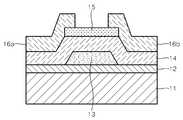
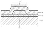
도 1 및 도 2는 본 발명의 실시예에 의한 산화물 반도체를 포함하는 박막 트랜지스터의 구조를 나타낸 단면도이다. 도 1에서는 바텀 게이트(bottom gate)형 박막 트랜지스터를 나타내었으며, 도 2에서는 탑 게이트(top gate)형 박막 트랜지스터를 나타내었다. 1 and 2 are cross-sectional views illustrating the structure of a thin film transistor including an oxide semiconductor according to an embodiment of the present invention. FIG. 1 shows a bottom gate type thin film transistor, and FIG. 2 shows a top gate type thin film transistor.
도 1을 참조하면, 본 발명의 실시예에 의한 산화물 박막 트랜지스터는 기판(11)의 일영역 상에 게이트 전극(13)이 형성되어 있으며, 기판(11) 및 게이트 전극(13) 상에 게이트 절연층(14)이 형성되어 있다. 기판(11)이 실리콘로 형성된 경우 실리콘 기판 표면에 열산화 공정에 의해 형성된 산화층(12)을 더 포함할 수 있 다. 게이트 전극(13)에 대응되는 게이트 절연층(14) 상에는 채널(15)이 형성되어 있으며, 채널(15)의 양측부 및 게이트 절연층(14) 상에는 소스(16a) 및 드레인(16b)이 형성되어 있다.1, an oxide thin film transistor according to an embodiment of the present invention includes a
도 2를 참조하면, 기판(101) 상에 소스(102a) 및 드레인(102b)이 형성되어 있으며, 소스(102a), 드레인(102b) 사이 영역에 채널(103)이 형성되어 있다. 채널(103) 및 기판(101) 상에는 게이트 절연층(104)이 형성되어 있으며, 채널(103)에 대응되는 게이트 절연층(104) 상에는 게이트 전극(105)이 형성되어 있다. 기판(101)이 실리콘으로 형성된 경우, 기판(101) 표면에는 열산화 공정에 의해 형성된 산화층을 더 포함할 수 있다.2, a
도 1 및 도 2에 나타낸 본 발명의 실시예에 의한 산화물 박막 트랜지스터를 형성하는 각 층의 형성 물질에 대해 상세하게 설명하면 다음과 같다.The formation materials of the respective layers forming the oxide thin film transistor according to the embodiment of the present invention shown in FIG. 1 and FIG. 2 will be described in detail as follows.
기판(11, 101)은 일반적인 반도체 소자에 사용되는 기판을 사용할 수 있으며, 예를 들어 실리콘, 글래스(glass) 또는 유기물 재료를 사용할 수 있다. 기판(11) 표면에 형성된 산화층(12)은 예를 들어 실리콘 기판을 열산화하여 형성된 실리콘 산화층(SiO2)일 수 있다. 게이트 전극(13, 105)은 전도성 물질을 사용할 수 있으며, 예를 들어 Ti, Pt, Ru, Au, Ag, Mo, Al, W 또는 Cu와 같은 금속 또는 IZO(InZnO) 또는 AZO(AlZnO)와 같은 금속 또는 전도성 산화물일 수 있다. 게이트 절연층(14, 104)은 통상적인 반도체 소자에 사용되는 절연 물질을 사용하여 형성할 수 있다. 예를 들어, SiO2또는 SiO2보다 유전율이 높은 High-K 물질인 HfO2, Al2O3, Si3N4 또는 이들의 혼합물을 사용할 수 있다. 소스(16a, 102a) 및 드레인(16b, 102b)은 전도성 물질을 사용하여 형성할 수 있으며, 예를 들어 Ti, Pt, Ru, Au, Ag, Mo, Al, W 또는 Cu와 같은 금속 또는 IZO(InZnO) 또는 AZO(AlZnO)와 같은 금속 또는 전도성 산화물을 사용할 수 있다.As the
이하, 도 3a 내지 도 3e를 참조하여 본 발명의 실시예에 의한 산화물 박막 트랜지스터의 제조 방법에 대해 설명하고자 한다. Hereinafter, a method of manufacturing an oxide thin film transistor according to an embodiment of the present invention will be described with reference to FIGS. 3A to 3E.
도 3a를 참조하면, 먼저 기판(11)을 마련한다. 기판(11)은 실리콘, 글래스 또는 유기물 재료로 형성할 수 있다. 만일, 실리콘을 기판(11)으로 사용하는 경우, 열산화 공정에 의해 기판(11) 표면에 절연층(12)을 형성할 수 있다. 그리고, 기판(11) 상에 금속 또는 전도성 금속 산화물 등의 전도성 물질(13a)을 도포한다.Referring to FIG. 3A, a
도 3b를 참조하면, 전도성 물질(13a)을 패터닝함으로써 게이트 전극(13)을 형성한다. 도 3c를 참조하면, 게이트 전극(13) 상에 절연 물질을 도포하고 패터닝하여 게이트 절연층(14)을 형성한다. 게이트 절연층(14)은 실리콘 산화물, 실리콘 질화물, 하프늄(Hf) 산화물, 알루미늄 산화물 또는 하프늄산화물 및 알루미늄산화물이 혼합물로 형성할 수 있다.Referring to FIG. 3B, the
도 3d를 참조하면, 게이트 절연층(14) 상에 채널 물질을 PVD, CVD 또는 ALD 등의 공정으로 도포한 뒤, 게이트(13)에 대응되는 게이트 절연층(14) 상에 채널 물질들이 잔류하도록 패터닝함으로써 채널(15)을 형성한다. 본 발명의 실시예에서 채 널(15)은 Zn 산화물 계열 물질에 란탄 계열 물질을 첨가하여 형성할 수 있다. 구체적으로 스퍼터링(sputtering) 공정으로 채널(15)을 형성하는 경우, Zn 산화물, In-Zn 산화물 또는 Ga-In-Zn 산화물 중 적어도 어느 하나로 형성된 타겟(target)과 란탄 계열 물질로 형성된 타겟을 챔버 내에 장착하여 코스퍼터링(cosputtering) 공정으로 채널(15)을 형성할 수 있다. 선택적으로 Zn 산화물 계열 물질과 란탄 계열 물질이 모두 포함된 하나의 단일 타겟을 사용할 수 있다. 상기 Zn 산화물 계열 물질에 란탄 계열 물질이 첨가된 산화물 반도체는 비정질이거나, 혼합결정질이거나 결정질일 수 있다.Referring to FIG. 3D, a channel material is applied on the
도 3e를 참조하면, 금속 또는 전도성 금속 산화물 등의 물질을 채널(15) 및 게이트 절연층(14) 상에 도포한 뒤, 채널(15)의 양측부에 연결되도록 패터닝함으로써 소스(16a) 및 드레인(16b)를 형성한다. 마지막으로, 섭씨 400도 이하의 온도에서 일반적인 퍼니스, RTA(rapid thermal annealing), 레이저 또는 핫플레이트에 등을 이용하여 열처리 공정을 실시한다.3E, a material such as a metal or a conductive metal oxide is applied on the
제조예 Manufacturing example
먼저, 표면에 실리콘 산화물이 100nm 두께로 형성된 실리콘 기판을 마련한다. 기판 표면에 Mo로 200nm 두께의 게이트 전극을 형성한 뒤, 기판 및 게이트 전극 상에 약 200nm 두께의 실리콘 질화물을 도포하여 게이트 절연층을 형성한다. 그리고, 게이트 전극에 대응되는 게이트 절연층 상에 산화물 반도체를 도포하여 채널을 형성한다. 채널 형성의 구체적인 공정을 설명하면 다음과 같다. 타겟으로는 일 본의 Kojundo 사에 In2O3:ZnO=1:2mol비가 되도록 주문하여 얻어진 99.99% In-Zn 산화물 타겟 및 LTS 사의 99.9% La 타겟을 각각 사용하였다. 이들 타겟들을 스퍼터(Varian사, 모델명 MS100)의 챔버 내에 장착시켰다. 증착 조건은 상온에서 O2 및 Ar 가스를 O2:Ar = 5:95 sccm 비율로 공급하면서 전체 가스 압력을 5mTorr로 유지하였으며, In-Zn 산화물 타겟에 150watt를 인가하고, Hf 타겟에 0, 15, 20, 25 및 30watt로 변화시키면서 전류를 인가하면서 코스퍼터링을 실시하였다. 그리하여, 약 70nm 두께로 In-Zn 산화물에 La가 포함된 산화물 반도체 박막을 도포하여 채널을 형성하였다. 그리고, 채널의 양측에 소스 및 드레인으로 Ti/Pt를 10/100nm 두께로 형성하였다.First, a silicon substrate having silicon oxide formed on its surface to a thickness of 100 nm is provided. A gate electrode having a thickness of 200 nm is formed on the substrate surface with Mo, and then a silicon nitride film having a thickness of about 200 nm is coated on the substrate and the gate electrode to form a gate insulating layer. Then, an oxide semiconductor is coated on the gate insulating layer corresponding to the gate electrode to form a channel. A concrete process of forming the channel will be described as follows. As the target, a 99.99% In-Zn oxide target and 99.9% La target of LTS, which were ordered so as to have a ratio of In2 O3 : ZnO = 1: 2 mol to Kojundo Company of Japan, were respectively used. These targets were mounted in a chamber of a sputtering machine (Varian, model name MS100). The deposition conditions were as follows: O2 and Ar gas were supplied at a ratio of O2 : Ar = 5:95 sccm at a room temperature while the total gas pressure was maintained at 5 mTorr, 150 watt was applied to the In-Zn oxide target, , 20, 25, and 30 watt while applying a current. Thus, a channel was formed by applying an oxide semiconductor thin film containing La to the In-Zn oxide to a thickness of about 70 nm. On both sides of the channel, Ti / Pt was formed to have a thickness of 10/100 nm as a source and a drain.
상술한 바와 같이 제조한 본 발명의 실시예에 의한 산화물 반도체에 대해 게이트 전압(Gate Voltage : Vg)에 대한 드레인 전류(Drain Current : Id) 값을 측정하였다.The drain current (Id ) value with respect to the gate voltage (Vg ) was measured for the oxide semiconductor according to the embodiment of the present invention.
도 4는 상술한 제조예에 의해 형성한 산화물 박막 트랜지스터에 대해 게이트 전압(Vg)에 대한 드레인 전류(Id) 값을 나타낸 도면이다. 여기서는, 산화물 박막 트랜지스터의 채널 형성을 위한 코스퍼터링 시 La의 첨가량을 조절하기 위해, In-Zn 산화물의 인가 전류를 고정시키고, La 타겟에 대한 증착 파워를 조절하기 위하여, 15W, 20W, 25W, 30W를 인가하여 형성한 시편 및 Hf를 포함하지 않고 형성한 시편(0W)에 대한 그래프를 나타내었다. 여기서, 트랜지스터의 게이트 폭 및 길이의 비(W/L)는 50/4㎛이며, 소스-드레인 전압(Vds)는 10.1V이다.4 is a diagram showing the value of the drain current Id with respect to the gate voltage Vg for the oxide thin film transistor formed by the above-described production example. Here, in order to control the addition amount of La during the co-sputtering for channel formation of the oxide thin film transistor, in order to fix the application current of the In-Zn oxide and control the deposition power to the La target, 15W, 20W, 25W, 30W And a specimen (0 W) formed without containing Hf. Here, the ratio (W / L) of the gate width to the length of the transistor is 50/4 占 퐉 and the source-drain voltage (Vds) is 10.1V.
도 4를 참조하면, In-Zn 산화물 내에 La가 포함되지 않은 In-Zn 산화물 채널의 경우, Von이 약 -2V이며, La 타겟에 대한 증착 파워가 증가하면서 그래프가 오른쪽으로 이동하여 La 타겟에 15W, 20W, 25W 및 30W를 인가한 경우, Von이 각각 8V, 10V, 15V 및 20V로 증가함을 알 수 있다. 여기서, La 타겟에 15W를 인가한 경우, 채널 이동도 Mobility는 약 4.4cm2/V.s를 나타내며, 전 시편을 통해 off 전류(Ioff) 값은 10pA 이하의 값을 나타낸다.Referring to FIG. 4, in the case of the In-Zn oxide channel not containing La in the In-Zn oxide, the Von is about -2 V, and the deposition power for the La target is increased, , 20W, 25W and 30W are applied, Von is increased to 8V, 10V, 15V and 20V, respectively. Here, when 15W is applied to the La target, the mobility of the channel is about 4.4 cm2 / Vs, and the off current (Ioff) value is 10 pA or less through all the specimens.
도 4에 나타낸 각각의 시편의 산화물 반도체 물질에 대해 조성을 검사하기 위하여 ICP(Inductively coupled plasma)-AES(Auger Electron Spectroscopy) 분석을 실시하였다. 분석기는 Shimadzu 사의 모델명 Shimadzu ICPS-8100 sequential spectrometer이었다. 각각의 시편에 따른 In, Zn 및 La의 조성을 분석한 결과를 표 1에 나타내었다.In order to examine the composition of the oxide semiconductor material of each specimen shown in FIG. 4, inductively coupled plasma (ICP) -AES (Auger Electron Spectroscopy) analysis was performed. The analyzer was a Shimadzu ICPS-8100 sequential spectrometer from Shimadzu. The compositions of In, Zn and La according to the respective specimens were analyzed and the results are shown in Table 1.
(at%)In / (In + Zn + La)
(at%)
(at%)Zn / (In + Zn + La)
(at%)
(at%)La / (In + Zn + La)
(at%)
※ 오차값 범위 : ±1%※ Error value range: ± 1%
표 1을 참조하면, La 타겟의 인가 전류를 증가시킬 수록 In-Zn 산화물에 대한 La의 첨가량이 증가하는 것을 확인할 수 있다. La 타겟의 인가 전류를 0W에서 30W 범위까지 증가시키는 경우, La의 함유량은 0 at% < La(at%) ≤ 11.4 at%, In의 조성비는 53.5 at% < In(at%) ≤ 55.5 at%이며, Zn의 조성비는 34.2 at% ≤ Zn(at%) < 46.5 at% 인 것을 알 수 있다. La의 조성이 증가함에 따라 In의 조성은 거의 변화가 없으나, Zn의 조성이 감소하는 것은 La가 Zn을 치환하여 산화물 반도체를 형성하는 것을 확인할 수 있다.Referring to Table 1, it can be seen that the amount of La added to the In-Zn oxide increases as the applied current of La target is increased. La (at%) ≤ 11.4 at%, and the composition ratio of In is 53.5 at% <In (at%) ≤ 55.5 at% , And the composition ratio of Zn is 34.2 at% ≤ Zn (at%) <46.5 at%. As the composition of La increases, the composition of In is almost unchanged. However, it is confirmed that the composition of Zn decreases because La substitutes for Zn to form an oxide semiconductor.
한편 증착된 박막의 조성성분비, 특성 그래프, 이동도 특성 등은 사용되는 타겟의 종류, 증착시 타겟 인가전압, 증착장비, 증착압력, 산소분압 조건, 기판온도 등에 의해 변경가능하다. 예를 들어, Zn 산화물 계열 타겟인 Zn 산화물, In-Zn 산화물 또는 Ga-In-Zn 산화물 타겟과 La 타겟의 2종류를 사용하여 코스퍼터링하는 경우에 대비하여 Ln-Zn 산화물, Ln-In-Zn 산화물 또는 Ln-Ga-In-Zn 산화물의 단일 타겟을 사용하는 경우 증착된 박막 조성이 달라질 수 있다. 또한 증착된 박막 조성이 같은 경우라도 증착 조건에 따라 박막 특성의 변경이 가능하다. 예를 들어 스퍼터링 공정으로 산화물 반도체를 증착하는 경우, 산소 분압에 따라 산화물의 저항 범위는 크게 변할 수 있다. 산소 분압이 적정량 이하로 조절되는 경우 증착된 박막의 저항이 낮은 박막을 증착할 수 있으며, 산소 분압을 높게 조절하는 경우 저항이 높은 박막을 증착할 수 있다.On the other hand, the composition ratio of the deposited thin film, the characteristic graph, and the mobility characteristics can be changed depending on the type of the target used, the target applied voltage at the time of deposition, the deposition equipment, the deposition pressure, the oxygen partial pressure condition, For example, in case of co-sputtering using Zn oxide, In-Zn oxide or Ga-In-Zn oxide target and La target, Zn oxide, Ln-In-Zn Oxide or a single target of an Ln-Ga-In-Zn oxide may be used, the deposited thin film composition may vary. Also, even if the deposited thin film composition is the same, the characteristics of the thin film can be changed according to the deposition conditions. For example, when an oxide semiconductor is deposited by a sputtering process, the resistance range of the oxide may vary greatly depending on the oxygen partial pressure. When the oxygen partial pressure is controlled to a proper amount or less, a thin film having a low resistance of the deposited thin film can be deposited, and a thin film having a high resistance can be deposited when the oxygen partial pressure is controlled to be high.
상술한 바와 같은 실시예를 통해서, 본 발명이 속하는 기술 분야에서 통상의 지식을 가진 자라면 본 발명의 기술적 사상에 의해 산화물 반도체를 이용하여 LCD, OLED 등 평판 디스플레이의 구동 트랜지스터, 메모리 소자의 주변회로 구성을 위한 트랜지스터나 산화물 인버터 등의 다양한 전자 소자를 제조할 수 있을 것이다. 본 발명의 실시예에 의한 산화물 박막 트랜지스터는 바텀 게이트형 또는 탑 게이트형으로 사용될 수 있다. 결과적으로 본 발명의 범위는 설명된 실시예에 의하여 정하여 질 것이 아니고 특허 청구범위에 기재된 기술적 사상에 의해 정하여져야 한다.It will be apparent to those skilled in the art that various modifications and variations can be made in the present invention without departing from the spirit or scope of the invention. Various electronic devices such as a transistor or an oxide inverter for constitution can be manufactured. The oxide thin film transistor according to an embodiment of the present invention can be used as a bottom gate type or a top gate type. As a result, the scope of the present invention is not to be determined by the described embodiments but should be determined by the technical idea described in the claims.
도 1 및 도 2는 본 발명의 실시예에 의한 산화물 반도체를 포함하는 박막 트랜지스터의 구조를 나타낸 단면도이다.1 and 2 are cross-sectional views illustrating the structure of a thin film transistor including an oxide semiconductor according to an embodiment of the present invention.
도 3a 내지 도 3e는 본 발명의 실시예에 의한 산화물 박막 트랜지스터의 제조 방법을 나타낸 도면이다.3A to 3E are views showing a method of manufacturing an oxide thin film transistor according to an embodiment of the present invention.
도 4는 채널 물질로 In-Zn 산화물에 La를 포함한 산화물 박막 트랜지스터에 대해 게이트 전압(Vg)에 대한 드레인 전류(Id) 값을 나타낸 도면이다.4 is a graph showing a drain current (Id ) value versus gate voltage (Vg ) for an oxide thin film transistor containing La as an In-Zn oxide as a channel material.
< 도면의 주요 부분에 대한 부호의 설명 >Description of the Related Art
11, 101... 기판 12... 절연층11, 101 ...
13, 105... 게이트 전극 14, 104... 게이트 절연층13, 105 ...
15... 채널 16a, 102a... 소스15 ...
16b, 102b... 드레인16b, 102b ... drain
Claims (24)
Translated fromKoreanPriority Applications (2)
| Application Number | Priority Date | Filing Date | Title |
|---|---|---|---|
| KR20080081073AKR101496150B1 (en) | 2008-08-19 | 2008-08-19 | Oxide Semiconductor and Thin Film Transistor comprising the same |
| US12/453,962US8373163B2 (en) | 2008-08-19 | 2009-05-28 | Oxide semiconductor and thin film transistor including the same |
Applications Claiming Priority (1)
| Application Number | Priority Date | Filing Date | Title |
|---|---|---|---|
| KR20080081073AKR101496150B1 (en) | 2008-08-19 | 2008-08-19 | Oxide Semiconductor and Thin Film Transistor comprising the same |
Publications (2)
| Publication Number | Publication Date |
|---|---|
| KR20100022408A KR20100022408A (en) | 2010-03-02 |
| KR101496150B1true KR101496150B1 (en) | 2015-02-27 |
Family
ID=41695518
Family Applications (1)
| Application Number | Title | Priority Date | Filing Date |
|---|---|---|---|
| KR20080081073AActiveKR101496150B1 (en) | 2008-08-19 | 2008-08-19 | Oxide Semiconductor and Thin Film Transistor comprising the same |
Country Status (2)
| Country | Link |
|---|---|
| US (1) | US8373163B2 (en) |
| KR (1) | KR101496150B1 (en) |
Families Citing this family (9)
| Publication number | Priority date | Publication date | Assignee | Title |
|---|---|---|---|---|
| KR101849321B1 (en)* | 2009-11-06 | 2018-04-16 | 가부시키가이샤 한도오따이 에네루기 켄큐쇼 | Semiconductor device and manufacturing method thereof |
| US8987728B2 (en) | 2011-03-25 | 2015-03-24 | Semiconductor Energy Laboratory Co., Ltd. | Semiconductor device and method of manufacturing semiconductor device |
| CN105931967B (en) | 2011-04-27 | 2019-05-03 | 株式会社半导体能源研究所 | Manufacturing method of semiconductor device |
| TWI422039B (en)* | 2011-05-11 | 2014-01-01 | Au Optronics Corp | Thin film transistor element and manufacturing method thereof |
| US9012993B2 (en)* | 2011-07-22 | 2015-04-21 | Semiconductor Energy Laboratory Co., Ltd. | Semiconductor device |
| US8994019B2 (en)* | 2011-08-05 | 2015-03-31 | Semiconductor Energy Laboratory Co., Ltd. | Semiconductor device |
| KR101891650B1 (en)* | 2011-09-22 | 2018-08-27 | 삼성디스플레이 주식회사 | OXIDE SEMICONDUCTOR, THIN FILM TRANSISTOR INCLUDING THE SAME AND THIN FILM TRANSISTOR array PANEL INCLUDING THE SAME |
| TWI661553B (en) | 2012-11-16 | 2019-06-01 | 日商半導體能源研究所股份有限公司 | Semiconductor device |
| CN110767745A (en)* | 2019-09-18 | 2020-02-07 | 华南理工大学 | Compound Metal Oxide Semiconductors and Thin Film Transistors and Their Applications |
Citations (1)
| Publication number | Priority date | Publication date | Assignee | Title |
|---|---|---|---|---|
| JP2007201366A (en)* | 2006-01-30 | 2007-08-09 | Canon Inc | Field effect transistor |
Family Cites Families (4)
| Publication number | Priority date | Publication date | Assignee | Title |
|---|---|---|---|---|
| JP2001148491A (en)* | 1999-11-19 | 2001-05-29 | Fuji Xerox Co Ltd | Photoelectric conversion element |
| JP2007059834A (en)* | 2005-08-26 | 2007-03-08 | Sharp Corp | Solid-state imaging device, manufacturing method thereof, and electronic information device |
| JP4932415B2 (en)* | 2006-09-29 | 2012-05-16 | 株式会社半導体エネルギー研究所 | Semiconductor device |
| JP4727684B2 (en)* | 2007-03-27 | 2011-07-20 | 富士フイルム株式会社 | Thin film field effect transistor and display device using the same |
- 2008
- 2008-08-19KRKR20080081073Apatent/KR101496150B1/enactiveActive
- 2009
- 2009-05-28USUS12/453,962patent/US8373163B2/ennot_activeExpired - Fee Related
Patent Citations (1)
| Publication number | Priority date | Publication date | Assignee | Title |
|---|---|---|---|---|
| JP2007201366A (en)* | 2006-01-30 | 2007-08-09 | Canon Inc | Field effect transistor |
Non-Patent Citations (1)
| Title |
|---|
| 논문1* |
Also Published As
| Publication number | Publication date |
|---|---|
| KR20100022408A (en) | 2010-03-02 |
| US8373163B2 (en) | 2013-02-12 |
| US20100044700A1 (en) | 2010-02-25 |
Similar Documents
| Publication | Publication Date | Title |
|---|---|---|
| KR101468594B1 (en) | Oxide semiconductor and thin film transistor including the same | |
| KR101468591B1 (en) | Oxide semiconductor and thin film transistor comprising the same | |
| US8450732B2 (en) | Oxide semiconductors and thin film transistors comprising the same | |
| JP5526023B2 (en) | Oxide semiconductor and thin film transistor including the same | |
| KR101552975B1 (en) | Oxide semiconductor and thin film transistor including the same | |
| KR101496150B1 (en) | Oxide Semiconductor and Thin Film Transistor comprising the same | |
| KR20090002841A (en) | Oxide semiconductor, thin film transistor comprising same, and method of manufacturing | |
| US8378342B2 (en) | Oxide semiconductor and thin film transistor including the same | |
| KR101468590B1 (en) | Oxide semiconductor and thin film transistor including the same | |
| KR101519480B1 (en) | Oxide Semiconductor and Thin Film Transistor comprising the same | |
| KR101600051B1 (en) | Oxide Semiconductor and Thin Film Transistor comprising the same | |
| KR102230653B1 (en) | Thin Film Transistor and Method of manufacturing the same | |
| KR20080111736A (en) | Oxide semiconductor and thin film transistor comprising the same | |
| KR20140050993A (en) | Zn compound semiconductor and thin film transistor comprising the same |
Legal Events
| Date | Code | Title | Description |
|---|---|---|---|
| PA0109 | Patent application | Patent event code:PA01091R01D Comment text:Patent Application Patent event date:20080819 | |
| PG1501 | Laying open of application | ||
| A201 | Request for examination | ||
| PA0201 | Request for examination | Patent event code:PA02012R01D Patent event date:20130812 Comment text:Request for Examination of Application Patent event code:PA02011R01I Patent event date:20080819 Comment text:Patent Application | |
| N231 | Notification of change of applicant | ||
| PN2301 | Change of applicant | Patent event date:20140821 Comment text:Notification of Change of Applicant Patent event code:PN23011R01D | |
| E902 | Notification of reason for refusal | ||
| PE0902 | Notice of grounds for rejection | Comment text:Notification of reason for refusal Patent event date:20140901 Patent event code:PE09021S01D | |
| E701 | Decision to grant or registration of patent right | ||
| PE0701 | Decision of registration | Patent event code:PE07011S01D Comment text:Decision to Grant Registration Patent event date:20141204 | |
| GRNT | Written decision to grant | ||
| PR0701 | Registration of establishment | Comment text:Registration of Establishment Patent event date:20150217 Patent event code:PR07011E01D | |
| PR1002 | Payment of registration fee | Payment date:20150223 End annual number:3 Start annual number:1 | |
| PG1601 | Publication of registration | ||
| FPAY | Annual fee payment | Payment date:20180119 Year of fee payment:4 | |
| PR1001 | Payment of annual fee | Payment date:20180119 Start annual number:4 End annual number:4 | |
| FPAY | Annual fee payment | Payment date:20190116 Year of fee payment:5 | |
| PR1001 | Payment of annual fee | Payment date:20190116 Start annual number:5 End annual number:5 | |
| FPAY | Annual fee payment | Payment date:20200120 Year of fee payment:6 | |
| PR1001 | Payment of annual fee | Payment date:20200120 Start annual number:6 End annual number:6 | |
| PR1001 | Payment of annual fee | Payment date:20210119 Start annual number:7 End annual number:7 | |
| PR1001 | Payment of annual fee | Payment date:20220119 Start annual number:8 End annual number:8 | |
| PR1001 | Payment of annual fee | Payment date:20230118 Start annual number:9 End annual number:9 | |
| PR1001 | Payment of annual fee | Payment date:20240119 Start annual number:10 End annual number:10 |