KR101496006B1 - Resistive random access memory(rram) structure and method of making the rram structure - Google Patents
Resistive random access memory(rram) structure and method of making the rram structureDownload PDFInfo
- Publication number
- KR101496006B1 KR101496006B1KR20130061662AKR20130061662AKR101496006B1KR 101496006 B1KR101496006 B1KR 101496006B1KR 20130061662 AKR20130061662 AKR 20130061662AKR 20130061662 AKR20130061662 AKR 20130061662AKR 101496006 B1KR101496006 B1KR 101496006B1
- Authority
- KR
- South Korea
- Prior art keywords
- gate
- rram
- bottom electrode
- transistor
- layer
- Prior art date
- Legal status (The legal status is an assumption and is not a legal conclusion. Google has not performed a legal analysis and makes no representation as to the accuracy of the status listed.)
- Active
Links
- 238000004519manufacturing processMethods0.000titleclaimsdescription18
- 239000000463materialSubstances0.000claimsabstractdescription60
- 239000004020conductorSubstances0.000claimsabstractdescription14
- 239000010410layerSubstances0.000claimsdescription82
- 238000000034methodMethods0.000claimsdescription33
- 239000000758substrateSubstances0.000claimsdescription33
- 239000003989dielectric materialSubstances0.000claimsdescription30
- 229910052751metalInorganic materials0.000claimsdescription30
- 239000002184metalSubstances0.000claimsdescription30
- 239000004065semiconductorSubstances0.000claimsdescription23
- 238000000151depositionMethods0.000claimsdescription14
- 125000006850spacer groupChemical group0.000claimsdescription12
- 229910021420polycrystalline siliconInorganic materials0.000claimsdescription9
- 229920005591polysiliconPolymers0.000claimsdescription9
- 238000000059patterningMethods0.000claimsdescription7
- 239000007772electrode materialSubstances0.000claimsdescription6
- NRTOMJZYCJJWKI-UHFFFAOYSA-NTitanium nitrideChemical compound[Ti]#NNRTOMJZYCJJWKI-UHFFFAOYSA-N0.000claimsdescription4
- 229910052782aluminiumInorganic materials0.000claimsdescription4
- 238000002955isolationMethods0.000claimsdescription4
- MZLGASXMSKOWSE-UHFFFAOYSA-Ntantalum nitrideChemical compound[Ta]#NMZLGASXMSKOWSE-UHFFFAOYSA-N0.000claimsdescription4
- 229910052719titaniumInorganic materials0.000claimsdescription4
- 239000010936titaniumSubstances0.000claimsdescription4
- 229910000449hafnium oxideInorganic materials0.000claimsdescription3
- WIHZLLGSGQNAGK-UHFFFAOYSA-Nhafnium(4+);oxygen(2-)Chemical compound[O-2].[O-2].[Hf+4]WIHZLLGSGQNAGK-UHFFFAOYSA-N0.000claimsdescription3
- 239000011229interlayerSubstances0.000claimsdescription3
- RVTZCBVAJQQJTK-UHFFFAOYSA-Noxygen(2-);zirconium(4+)Chemical compound[O-2].[O-2].[Zr+4]RVTZCBVAJQQJTK-UHFFFAOYSA-N0.000claimsdescription3
- 229910001928zirconium oxideInorganic materials0.000claimsdescription3
- GWEVSGVZZGPLCZ-UHFFFAOYSA-NTitan oxideChemical compoundO=[Ti]=OGWEVSGVZZGPLCZ-UHFFFAOYSA-N0.000claimsdescription2
- RTAQQCXQSZGOHL-UHFFFAOYSA-NTitaniumChemical compound[Ti]RTAQQCXQSZGOHL-UHFFFAOYSA-N0.000claimsdescription2
- XAGFODPZIPBFFR-UHFFFAOYSA-NaluminiumChemical compound[Al]XAGFODPZIPBFFR-UHFFFAOYSA-N0.000claimsdescription2
- 238000002513implantationMethods0.000claimsdescription2
- 229910000480nickel oxideInorganic materials0.000claimsdescription2
- TWNQGVIAIRXVLR-UHFFFAOYSA-Noxo(oxoalumanyloxy)alumaneChemical compoundO=[Al]O[Al]=OTWNQGVIAIRXVLR-UHFFFAOYSA-N0.000claimsdescription2
- GNRSAWUEBMWBQH-UHFFFAOYSA-NoxonickelChemical compound[Ni]=OGNRSAWUEBMWBQH-UHFFFAOYSA-N0.000claimsdescription2
- BPUBBGLMJRNUCC-UHFFFAOYSA-Noxygen(2-);tantalum(5+)Chemical compound[O-2].[O-2].[O-2].[O-2].[O-2].[Ta+5].[Ta+5]BPUBBGLMJRNUCC-UHFFFAOYSA-N0.000claimsdescription2
- 229910001936tantalum oxideInorganic materials0.000claimsdescription2
- OGIDPMRJRNCKJF-UHFFFAOYSA-Ntitanium oxideInorganic materials[Ti]=OOGIDPMRJRNCKJF-UHFFFAOYSA-N0.000claimsdescription2
- 230000008569processEffects0.000description20
- 238000010586diagramMethods0.000description14
- 229920002120photoresistant polymerPolymers0.000description10
- XUIMIQQOPSSXEZ-UHFFFAOYSA-NSiliconChemical compound[Si]XUIMIQQOPSSXEZ-UHFFFAOYSA-N0.000description9
- 235000012431wafersNutrition0.000description9
- VYPSYNLAJGMNEJ-UHFFFAOYSA-NSilicium dioxideChemical compoundO=[Si]=OVYPSYNLAJGMNEJ-UHFFFAOYSA-N0.000description8
- 238000005229chemical vapour depositionMethods0.000description8
- 229910052710siliconInorganic materials0.000description8
- 239000010703siliconSubstances0.000description8
- 239000007943implantSubstances0.000description6
- 229910052814silicon oxideInorganic materials0.000description6
- 229910052581Si3N4Inorganic materials0.000description5
- QVGXLLKOCUKJST-UHFFFAOYSA-Natomic oxygenChemical compound[O]QVGXLLKOCUKJST-UHFFFAOYSA-N0.000description5
- 230000015572biosynthetic processEffects0.000description5
- 229910044991metal oxideInorganic materials0.000description5
- 150000004706metal oxidesChemical class0.000description5
- 239000001301oxygenSubstances0.000description5
- 229910052760oxygenInorganic materials0.000description5
- BASFCYQUMIYNBI-UHFFFAOYSA-NplatinumChemical compound[Pt]BASFCYQUMIYNBI-UHFFFAOYSA-N0.000description5
- HQVNEWCFYHHQES-UHFFFAOYSA-Nsilicon nitrideChemical compoundN12[Si]34N5[Si]62N3[Si]51N64HQVNEWCFYHHQES-UHFFFAOYSA-N0.000description5
- 238000000231atomic layer depositionMethods0.000description4
- 239000010949copperSubstances0.000description4
- 229910021332silicideInorganic materials0.000description4
- FVBUAEGBCNSCDD-UHFFFAOYSA-Nsilicide(4-)Chemical compound[Si-4]FVBUAEGBCNSCDD-UHFFFAOYSA-N0.000description4
- 229910052718tinInorganic materials0.000description4
- 229910052723transition metalInorganic materials0.000description4
- 150000003624transition metalsChemical class0.000description4
- ATJFFYVFTNAWJD-UHFFFAOYSA-NTinChemical compound[Sn]ATJFFYVFTNAWJD-UHFFFAOYSA-N0.000description3
- 229910045601alloyInorganic materials0.000description3
- 239000000956alloySubstances0.000description3
- 229910052802copperInorganic materials0.000description3
- 150000004767nitridesChemical class0.000description3
- 238000005240physical vapour depositionMethods0.000description3
- 229910052707rutheniumInorganic materials0.000description3
- 229910052715tantalumInorganic materials0.000description3
- OKTJSMMVPCPJKN-UHFFFAOYSA-NCarbonChemical compound[C]OKTJSMMVPCPJKN-UHFFFAOYSA-N0.000description2
- KRHYYFGTRYWZRS-UHFFFAOYSA-MFluoride anionChemical compound[F-]KRHYYFGTRYWZRS-UHFFFAOYSA-M0.000description2
- 229910001362Ta alloysInorganic materials0.000description2
- 229910004166TaNInorganic materials0.000description2
- 229910010037TiAlNInorganic materials0.000description2
- 229910052799carbonInorganic materials0.000description2
- 239000002131composite materialSubstances0.000description2
- 150000001875compoundsChemical class0.000description2
- 238000005520cutting processMethods0.000description2
- 238000005530etchingMethods0.000description2
- 239000010931goldSubstances0.000description2
- AMGQUBHHOARCQH-UHFFFAOYSA-Nindium;oxotinChemical compound[In].[Sn]=OAMGQUBHHOARCQH-UHFFFAOYSA-N0.000description2
- 239000012212insulatorSubstances0.000description2
- 229910052741iridiumInorganic materials0.000description2
- ULFQGKXWKFZMLH-UHFFFAOYSA-Niridium tantalumChemical compound[Ta].[Ir]ULFQGKXWKFZMLH-UHFFFAOYSA-N0.000description2
- 230000007246mechanismEffects0.000description2
- 229910052697platinumInorganic materials0.000description2
- HBMJWWWQQXIZIP-UHFFFAOYSA-Nsilicon carbideChemical compound[Si+]#[C-]HBMJWWWQQXIZIP-UHFFFAOYSA-N0.000description2
- 229910010271silicon carbideInorganic materials0.000description2
- 229910052721tungstenInorganic materials0.000description2
- 229910018072Al 2 O 3Inorganic materials0.000description1
- IJGRMHOSHXDMSA-UHFFFAOYSA-NAtomic nitrogenChemical compoundN#NIJGRMHOSHXDMSA-UHFFFAOYSA-N0.000description1
- RYGMFSIKBFXOCR-UHFFFAOYSA-NCopperChemical compound[Cu]RYGMFSIKBFXOCR-UHFFFAOYSA-N0.000description1
- KJTLSVCANCCWHF-UHFFFAOYSA-NRutheniumChemical compound[Ru]KJTLSVCANCCWHF-UHFFFAOYSA-N0.000description1
- 229910000577Silicon-germaniumInorganic materials0.000description1
- 229910006404SnO 2Inorganic materials0.000description1
- 229910010413TiO 2Inorganic materials0.000description1
- 229910008599TiWInorganic materials0.000description1
- GEIAQOFPUVMAGM-UHFFFAOYSA-NZrOInorganic materials[Zr]=OGEIAQOFPUVMAGM-UHFFFAOYSA-N0.000description1
- LEVVHYCKPQWKOP-UHFFFAOYSA-N[Si].[Ge]Chemical compound[Si].[Ge]LEVVHYCKPQWKOP-UHFFFAOYSA-N0.000description1
- 230000004075alterationEffects0.000description1
- 238000000137annealingMethods0.000description1
- 238000003491arrayMethods0.000description1
- 230000008859changeEffects0.000description1
- 238000003486chemical etchingMethods0.000description1
- 238000006243chemical reactionMethods0.000description1
- 229910052804chromiumInorganic materials0.000description1
- 238000010276constructionMethods0.000description1
- 230000003247decreasing effectEffects0.000description1
- 230000007547defectEffects0.000description1
- 230000008021depositionEffects0.000description1
- 238000005137deposition processMethods0.000description1
- 229910001873dinitrogenInorganic materials0.000description1
- 239000002019doping agentSubstances0.000description1
- 238000000313electron-beam-induced depositionMethods0.000description1
- 238000005516engineering processMethods0.000description1
- 229910052732germaniumInorganic materials0.000description1
- GNPVGFCGXDBREM-UHFFFAOYSA-Ngermanium atomChemical compound[Ge]GNPVGFCGXDBREM-UHFFFAOYSA-N0.000description1
- PCHJSUWPFVWCPO-UHFFFAOYSA-NgoldChemical compound[Au]PCHJSUWPFVWCPO-UHFFFAOYSA-N0.000description1
- 229910052737goldInorganic materials0.000description1
- 229910052735hafniumInorganic materials0.000description1
- 238000002347injectionMethods0.000description1
- 239000007924injectionSubstances0.000description1
- GKOZUEZYRPOHIO-UHFFFAOYSA-Niridium atomChemical compound[Ir]GKOZUEZYRPOHIO-UHFFFAOYSA-N0.000description1
- 229910052742ironInorganic materials0.000description1
- 239000011159matrix materialSubstances0.000description1
- 150000002739metalsChemical class0.000description1
- 230000005012migrationEffects0.000description1
- 238000013508migrationMethods0.000description1
- 229910052759nickelInorganic materials0.000description1
- PXHVJJICTQNCMI-UHFFFAOYSA-NnickelSubstances[Ni]PXHVJJICTQNCMI-UHFFFAOYSA-N0.000description1
- 230000003287optical effectEffects0.000description1
- 238000000206photolithographyMethods0.000description1
- 238000000623plasma-assisted chemical vapour depositionMethods0.000description1
- 239000002243precursorSubstances0.000description1
- 230000005855radiationEffects0.000description1
- 235000012239silicon dioxideNutrition0.000description1
- 239000000377silicon dioxideSubstances0.000description1
- 238000004544sputter depositionMethods0.000description1
- 238000006467substitution reactionMethods0.000description1
- GUVRBAGPIYLISA-UHFFFAOYSA-Ntantalum atomChemical compound[Ta]GUVRBAGPIYLISA-UHFFFAOYSA-N0.000description1
- VSSLEOGOUUKTNN-UHFFFAOYSA-Ntantalum titaniumChemical compound[Ti].[Ta]VSSLEOGOUUKTNN-UHFFFAOYSA-N0.000description1
- 229910000314transition metal oxideInorganic materials0.000description1
- 229910021350transition metal silicideInorganic materials0.000description1
- WFKWXMTUELFFGS-UHFFFAOYSA-NtungstenChemical compound[W]WFKWXMTUELFFGS-UHFFFAOYSA-N0.000description1
- 239000010937tungstenSubstances0.000description1
- 238000007740vapor depositionMethods0.000description1
- 229910052726zirconiumInorganic materials0.000description1
Images


Classifications
- H—ELECTRICITY
- H10—SEMICONDUCTOR DEVICES; ELECTRIC SOLID-STATE DEVICES NOT OTHERWISE PROVIDED FOR
- H10N—ELECTRIC SOLID-STATE DEVICES NOT OTHERWISE PROVIDED FOR
- H10N70/00—Solid-state devices having no potential barriers, and specially adapted for rectifying, amplifying, oscillating or switching
- H10N70/20—Multistable switching devices, e.g. memristors
- H—ELECTRICITY
- H10—SEMICONDUCTOR DEVICES; ELECTRIC SOLID-STATE DEVICES NOT OTHERWISE PROVIDED FOR
- H10B—ELECTRONIC MEMORY DEVICES
- H10B63/00—Resistance change memory devices, e.g. resistive RAM [ReRAM] devices
- H10B63/30—Resistance change memory devices, e.g. resistive RAM [ReRAM] devices comprising selection components having three or more electrodes, e.g. transistors
- H—ELECTRICITY
- H10—SEMICONDUCTOR DEVICES; ELECTRIC SOLID-STATE DEVICES NOT OTHERWISE PROVIDED FOR
- H10B—ELECTRONIC MEMORY DEVICES
- H10B63/00—Resistance change memory devices, e.g. resistive RAM [ReRAM] devices
- H10B63/80—Arrangements comprising multiple bistable or multi-stable switching components of the same type on a plane parallel to the substrate, e.g. cross-point arrays
- H—ELECTRICITY
- H10—SEMICONDUCTOR DEVICES; ELECTRIC SOLID-STATE DEVICES NOT OTHERWISE PROVIDED FOR
- H10N—ELECTRIC SOLID-STATE DEVICES NOT OTHERWISE PROVIDED FOR
- H10N70/00—Solid-state devices having no potential barriers, and specially adapted for rectifying, amplifying, oscillating or switching
- H10N70/011—Manufacture or treatment of multistable switching devices
- H10N70/061—Shaping switching materials
- H10N70/063—Shaping switching materials by etching of pre-deposited switching material layers, e.g. lithography
- H—ELECTRICITY
- H10—SEMICONDUCTOR DEVICES; ELECTRIC SOLID-STATE DEVICES NOT OTHERWISE PROVIDED FOR
- H10N—ELECTRIC SOLID-STATE DEVICES NOT OTHERWISE PROVIDED FOR
- H10N70/00—Solid-state devices having no potential barriers, and specially adapted for rectifying, amplifying, oscillating or switching
- H10N70/011—Manufacture or treatment of multistable switching devices
- H10N70/061—Shaping switching materials
- H10N70/068—Shaping switching materials by processes specially adapted for achieving sub-lithographic dimensions, e.g. using spacers
- H—ELECTRICITY
- H10—SEMICONDUCTOR DEVICES; ELECTRIC SOLID-STATE DEVICES NOT OTHERWISE PROVIDED FOR
- H10N—ELECTRIC SOLID-STATE DEVICES NOT OTHERWISE PROVIDED FOR
- H10N70/00—Solid-state devices having no potential barriers, and specially adapted for rectifying, amplifying, oscillating or switching
- H10N70/801—Constructional details of multistable switching devices
- H10N70/821—Device geometry
- H10N70/826—Device geometry adapted for essentially vertical current flow, e.g. sandwich or pillar type devices
- H—ELECTRICITY
- H10—SEMICONDUCTOR DEVICES; ELECTRIC SOLID-STATE DEVICES NOT OTHERWISE PROVIDED FOR
- H10N—ELECTRIC SOLID-STATE DEVICES NOT OTHERWISE PROVIDED FOR
- H10N70/00—Solid-state devices having no potential barriers, and specially adapted for rectifying, amplifying, oscillating or switching
- H10N70/801—Constructional details of multistable switching devices
- H10N70/841—Electrodes
- H—ELECTRICITY
- H10—SEMICONDUCTOR DEVICES; ELECTRIC SOLID-STATE DEVICES NOT OTHERWISE PROVIDED FOR
- H10N—ELECTRIC SOLID-STATE DEVICES NOT OTHERWISE PROVIDED FOR
- H10N70/00—Solid-state devices having no potential barriers, and specially adapted for rectifying, amplifying, oscillating or switching
- H10N70/801—Constructional details of multistable switching devices
- H10N70/881—Switching materials
- H10N70/883—Oxides or nitrides
- H10N70/8833—Binary metal oxides, e.g. TaOx
Landscapes
- Engineering & Computer Science (AREA)
- Manufacturing & Machinery (AREA)
- Semiconductor Memories (AREA)
Abstract
Translated fromKoreanDescription
Translated fromKorean본 개시는 반도체 장치에 관한 것으로서, 보다 구체적으로는 저항성 랜덤 액세스 메모리(RRAM; resistive random-access memory) 장치 구조체 및 RRAM 장치의 제조 방법에 관한 것이다.The present disclosure relates to semiconductor devices, and more particularly to resistive random-access memory (RRAM) device structures and methods of manufacturing RRAM devices.
집적 회로(IC; integrated circuit) 장치에서, 저항성 랜덤 액세스 메모리(RRAM)는 차세대 비휘발성 메모리 장치용의 최근 기술이다. RRAM은 전하가 아니라 저항값을 이용하여 많은 데이터를 각각 저장하는 RRAM 셀의 어레이를 포함하는 메모리 구조체이다. 특히, 각 RRAM 셀은 저항성 물질층을 포함하고, 이 물질층의 저항은 논리값 "0" 또는 논리값 "1"을 나타내도록 조절될 수 있다. RRAM 장치는 보통은 절연성인 유전체가 충분히 높은 전압의 인가 후에 형성되는 필라멘트 또는 전도 경로를 통해 전도하도록 될 수 있다는 원리로 작동한다. 필라멘트 또는 전도 경로의 형성은 RRAM의 형성 작업 또는 형성 프로세스이다. 충분히 높은 전압은 '형성' 전압이다. 전도 경로 형성은 결손, 금속 이동, 및 기타 메카니즘을 비롯하여 상이한 메카니즘으로부터 생길 수 있다. 다양한 여러 유전체 물질이 RRAM 장치에 사용될 수 있다. 일단 필라멘트 또는 전도 경로가 형성되면, 재설정, 즉 파괴될 수 있어, 높은 저항을 초래하거나 설정, 즉 재형성되어 적절하게 인가된 전압에 의해 보다 낮은 저항을 초래한다. RRAM 셀의 어레이를 구성하는 다양한 아키텍처가 존재한다. 예컨대, 횡단점 아키텍처가 워드 라인과 비트 라인을 가로질러 사이에 구성되는 각 셀에 RRAM을 포함한다. 다른 예에서, 트랜지스터 타입 아키텍처가 각 셀에서 RRAM을 트랜지스터와 한쌍이 되게 하고(1T1R), 셀 영역의 비용으로 랜덤 액세스 시간을 개선시킨다. 또한, 1T1R 아키텍처는 더 많은 물질층과 적어도 3개의 추가 포토마스크, 이에 따라 더 많은 처리 단계와 더 많은 제조 비용을 필요로 한다.BACKGROUND OF THE INVENTION In integrated circuit (IC) devices, resistive random access memory (RRAM) is a recent technology for next generation non-volatile memory devices. The RRAM is a memory structure including an array of RRAM cells storing a large amount of data using resistances rather than charges. In particular, each RRAM cell comprises a layer of resistive material, and the resistance of this layer of material can be adjusted to represent a logic value "0" or a logic value "1". RRAM devices operate on the principle that usually dielectric dielectrics can be made to conduct through filaments or conduction paths formed after application of a sufficiently high voltage. The formation of the filament or conduction path is the formation or formation process of the RRAM. A sufficiently high voltage is a 'forming' voltage. Conductive path formation can result from different mechanisms, including defects, metal migration, and other mechanisms. A variety of different dielectric materials can be used in RRAM devices. Once the filament or conduction path is formed, it can be reset, i.e., broken, resulting in a high resistance or set, i.e., reformed, resulting in a lower resistance due to a suitably applied voltage. There are various architectures that constitute an array of RRAM cells. For example, a cross-point architecture includes an RRAM in each cell that is constructed between a word line and a bit line. In another example, a transistor type architecture causes the RRAM to pair with the transistors (1T1R) in each cell and improve the random access time at the cost of the cell area. In addition, the 1T1R architecture requires more material layers and at least three additional photomasks, thus more processing steps and more manufacturing costs.
따라서, 개선된 RRAM 구조체 및 제조 방법을 계속 추구하고 있다.Accordingly, there is an ongoing pursuit of improved RRAM structures and fabrication methods.
본 발명은 저항성 랜덤 액세스 메모리(RRAM) 셀을 제공한다. RRAM 셀은 트랜지스터, 트랜지스터의 드레인 영역에 인접하고 게이트와 동일 평면 상에 있는 바닥 전극, 바닥 전극 상의 저항성 물질층, 저항성 물질층 상의 상부 전극, 및 바닥 전극을 드레인 영역에 연결하는 전도성 물질을 포함한다.The present invention provides a resistive random access memory (RRAM) cell. The RRAM cell includes a transistor, a bottom electrode adjacent to the drain region of the transistor and coplanar with the gate, a resistive material layer on the bottom electrode, an upper electrode on the resistive material layer, and a conductive material connecting the bottom electrode to the drain region .
본 개시의 양태는 첨부 도면과 함께 읽을 때에 이하의 상세한 설명으로부터 가장 잘 이해된다. 산업에 있어서의 표준적 실시에 따라, 다양한 특징부들은 실척으로 도시되지 않는다는 점을 강조한다. 사실상, 다양한 특징부들의 치수는 논의의 명확도를 위해 임의로 증가 또는 감소된다.
도 1은 저항성 랜덤 액세스 메모리(RRAM) 구조체의 단면도이다.
도 2는 본 개시의 다양한 실시예에 따른 메모리 셀의 단면도이다.
도 3은 본 개시의 다양한 실시예에 따른 도 2의 메모리 셀을 갖는 메모리 셀 어레이의 일부의 레이아웃 다이어그램이다.
도 4는 다양한 실시예에서 본 개시의 양태에 따라 구성된 메모리 장치를 제조하는 방법의 흐름도이다.
도 5a, 5b, 6a, 6b, 7a, 7b, 8a, 8b, 9a 및 9b는 본 개시의 다양한 실시예에 따라 부분적으로 제조된 메모리 셀의 단면도이다.
도 5c는 본 개시의 다양한 실시예에 따라 도 5a 및 도 5b의 부분적으로 제조된 메모리 셀을 갖는 메모리 셀 어레이의 일부의 레이아웃 다이어그램이다.
도 7c는 본 개시의 다양한 실시예에 따라 도 7a 및 도 7b의 부분적으로 제조된 메모리 셀을 갖는 메모리 셀 어레이의 일부의 레이아웃 다이어그램이다.
도 9c는 본 개시의 다양한 실시예에 따라 도 9a 및 도 9b의 부분적으로 제조된 메모리 셀을 갖는 메모리 셀 어레이의 일부의 레이아웃 다이어그램이다.
도 10a 내지 10e 및 도 11a 내지 11e는 본 개시의 다양한 실시예에 따라 부분적으로 제조된 메모리 셀의 단면도이다.Embodiments of the disclosure are best understood from the following detailed description when read in conjunction with the accompanying drawings. Emphasize that, according to standard practice in industry, the various features are not shown to scale. Indeed, the dimensions of the various features are optionally increased or decreased for clarity of discussion.
1 is a cross-sectional view of a resistive random access memory (RRAM) structure.
2 is a cross-sectional view of a memory cell according to various embodiments of the present disclosure;
Figure 3 is a layout diagram of a portion of a memory cell array having memory cells of Figure 2 in accordance with various embodiments of the present disclosure.
4 is a flow diagram of a method of fabricating a memory device constructed in accordance with aspects of the present disclosure in various embodiments.
Figures 5A, 5B, 6A, 6B, 7A, 7B, 8A, 8B, 9A and 9B are cross-sectional views of partially fabricated memory cells according to various embodiments of the present disclosure.
5C is a layout diagram of a portion of a memory cell array having partially fabricated memory cells of FIGS. 5A and 5B in accordance with various embodiments of the present disclosure.
Figure 7C is a layout diagram of a portion of a memory cell array having partially fabricated memory cells of Figures 7A and 7B in accordance with various embodiments of the present disclosure.
9C is a layout diagram of a portion of a memory cell array having partially fabricated memory cells of FIGS. 9A and 9B in accordance with various embodiments of the present disclosure.
10A-10E and 11A-11E are cross-sectional views of a partially fabricated memory cell in accordance with various embodiments of the present disclosure.
이하의 개시는 다양한 실시예들의 상이한 특징부들을 실시하기 위한 많은 상이한 실시예, 즉 예를 제공한다는 것을 알아야 한다. 구성요소 및 구조의 특정한 예는 본 개시를 간소화하도록 아래에서 설명된다. 물론, 이들은 단지 예일 뿐이고 한정하도록 의도되지 않는다. 또한, 본 개시는 다양한 예에서 참조 번호 및/또는 문자를 반복할 수 있다. 이 반복은 간소화 및 명확도를 위한 것이고 논의되는 다양한 실시예들 및/또는 구성들 간의 관계를 자체가 결정하지 않는다.It should be noted that the following disclosure provides many different embodiments, i. E., Examples for implementing different features of the various embodiments. Specific examples of components and structures are described below to simplify the present disclosure. Of course, these are merely examples and are not intended to be limiting. In addition, the present disclosure may repeat the reference numerals and / or characters in various examples. This iteration is for simplicity and clarity and does not itself determine the relationship between the various embodiments and / or configurations discussed.
또한, "밑에", "아래에", "하부", "위에", "상부" 등과 같이 공간적으로 상대적인 용어는 본 명세서에서 도면에 예시된 바와 같이 다른 요소(들) 또는 특징부(들)에 대한 하나의 요소 또는 특징부의 관계를 설명하도록 설명의 용이함을 위해 사용될 수 있다. 공간적으로 상대적인 용어는 도면에 도시된 배향 외에 사용 또는 작동 시에 장치의 상이한 배향을 포함하도록 의도된다. 예컨대, 도면의 장치가 역전되면, 다른 요소 또는 특징부의 "아래에" 또는 "밑에" 있는 것으로 설명된 요소는 다른 요소 또는 특징부의 "위로" 배향되게 된다. 따라서, 예시적인 용어 "아래에"는 위 및 아래의 배향 모두를 포함할 수 있다.Also, terms spatially relative, such as "below," "below," "below," "above," "above," and the like are used herein to refer to the other element (s) or feature May be used for ease of explanation to illustrate the relationship of one element or feature to another. Spatially relative terms are intended to encompass different orientations of the device in use or operation in addition to the orientation shown in the figures. For example, when an apparatus in the drawings is reversed, elements described as being "under" or "under" other elements or features are oriented "up" over other elements or features. Thus, the exemplary term "below" may include both orientation above and below.
논의된 바와 같이, 저항성 랜덤 액세스 메모리(RRAM) 구조체는 도 1에 도시된 바와 같이 2개의 전극 간에 저항성 물질층을 포함한다. RRAM 구조체(100)는 기판(102) 위의 바닥 전극(104), 저항성 물질층(106), 및 상부 전극(110)을 포함한다. RRAM 구조체(100)는 상이한 전기 저항값을 갖는 2개 이상의 상태를 가질 수 있다. 각 상태는 상이한 디지털값을 나타낼 수 있다. RRAM 구조체(100)는 예정된 전압 또는 전류를 RRAM 구조체(100)에 인가함으로써 한 상태를 다른 상태로 전환시킬 수 있다. 예컨대, RRAM 구조체(100)는 "고저항 상태"로서 지칭되는 비교적 높은 저항의 상태와, "저저항 상태"로서 지칭되는 비교적 낮은 저항의 상태를 갖는다. RRAM 구조체(100)는 예정된 전압 또는 전류를 인가함으로써 고저항 상태로부터 저저항 상태로, 또는 저저항 상태로부터 고저항 상태로 전환될 수 있다.As discussed, a resistive random access memory (RRAM) structure includes a layer of resistive material between two electrodes, as shown in FIG. The
기판(102)은 실리콘 기판 등의 반도체 프로세스에 채용된 기판일 수 있다. 기판(102)은 벌크 기판일 수 있고, 장치 또는 절연 구조체를 포함할 수 있다. 도 1은 예시를 간소화하기 위하여 단순한 직사각형의 기판(102)을 예시하고 있다.The
하나의 트랜지스터와 하나의 RRAM을 갖는 메모리 비트 셀(1T1R)에서, 바닥 전극(104)은 금(Au), 플라티늄(Pt), 루테늄(Ru), 이리듐(Ir), 티타늄(Ti), 알루미늄(Al), 구리(Cu), 탄탈(Ta), 텅스텐(W), 이리듐-탄탈 합금(Ir-Ta) 또는 인듐-주석 산화물(ITO), 또는 TaN, TiN, TiAlN, TiW와 같은 이들의 임의의 합금, 산화물, 질화물, 불화물, 탄화물, 붕소화물 또는 규화물, 또는 그 조합물로 제조될 수 있다. 바닥(104B)으로부터 상단(104A)까지 바닥 전극의 두께는 약 100-500 nm의 범위일 수 있다. 일 실시예에서, 바닥 전극은 탄탈 질화물층과 티타늄 질화물층을 포함한다.In the memory bit cell 1T1R having one transistor and one RRAM, the
저항성 물질층(106)은 바닥 전극(104) 상에 형성되고 바닥 전극(104)과 직접 접촉한다. 저항성 물질층(106)의 두께는 약 20 내지 100 nm의 범위일 수 있다. 저항성 물질층은 W, Ta, Ti, Ni, Co, Hf, Ru, Zr, Fe, Sn, Al, Cu, Ag, Mo, Cr의 하나 이상의 산화물을 포함할 수 있다. 몇몇의 경우에, 실리콘은 복합 물질을 형성한다. 몇몇 실시예에서, 하프늄 산화물 및/또는 지르코늄 산화물이 사용된다.A layer of
상부 전극(110)은 저항성 물질층(106) 또는 선택적 덮개층(108) 위에 형성된다. 상부 전극(110)은 금(Au), 플라티늄(Pt), 루테늄(Ru), 이리듐(Ir), 티타늄(Ti), 알루미늄(Al), 구리(Cu), 탄탈(Ta), 텅스텐(W), 이리듐-탄탈 합금(Ir-Ta) 또는 인듐-주석 산화물(ITO), 또는 TaN, TiN, TiAlN, TiW와 같은 이들의 임의의 합금, 산화물, 질화물, 불화물, 탄화물, 붕소화물 또는 규화물, 또는 그 조합물로 제조될 수 있다. 상부 전극(110)의 두께는 100-500 nm의 범위일 수 있다.An
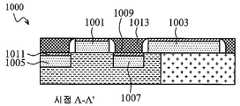
도 2는 본 개시의 다양한 실시예에 따른 메모리 셀(200)의 단면도이다. 메모리 셀(200)은 트랜지스터 부분(201)과 RRAM 구조체 부분(203)을 포함한다. 트랜지스터 부분(201)은 기판(202) 내에 게이트(207), 소스 영역(209), 드레인 영역(211), 하나 이상의 저 도핑 드레인(LDD; lightly-doped drain) 영역(213), 및 게이트(207) 아래의 채널 영역(217)을 포함한다. 게이트(207)는 게이트 유전체(219)와 스페이서(215)를 포함하는 폴리실리콘 게이트 또는 고유전율(high-k) 게이트일 수 있다. 게이트(207)의 전도성 부분은 하나 이상의 층 또는 복합 구조체를 포함할 수 있다. 일 실시예에서, 폴리실리콘 게이트(207)는 또한 상단에 살리사이드(salicided; 자기 정렬된 규화물) 영역을 포함한다. 다른 실시예에서, 고유전율(high-k) 금속 게이트(207)는 알루미늄, 티타늄, 티타늄 질화물, 탄탈 질화물, 및 금속 게이트에 사용되는 기타 공지된 금속 및 화합물 중 하나 이상을 포함하는 물질을 포함한다.2 is a cross-sectional view of a
트랜지스터 부분(201) 옆에는 RRAM 구조체 부분(203)이 있다. 도 1과 관련하여 논의된 바와 같이, RRAM 구조체 부분(203)은 바닥 전극, 저항성 물질층, 및 상부 전극을 스택 형태로 포함한다. 바닥 전극(221)은 저항성 물질층(227) 및 상부 전극(229)보다 넓다. 바닥 전극(221)은 게이트 스택으로부터 트랜지스터 드레인 영역(211)을 가로질러 배치되는 동시에 형성된다. 저항성 물질층(227)과 상부 전극(229)은 트랜지스터 드레인 영역(211)으로부터 멀어지게 바닥 전극(221)의 일부 상에 배치된다. 도 2에 도시된 바와 같이, 저항성 물질층(227)과 상부 전극(229)은 양면 상의 부분을 차지하지 않도록 바닥 전극의 중간 단면 상에 배치된다. 저항성 물질층(227)과 상부 전극(229)이 상부에 없는 바닥 전극(221)의 부분은 트랜지스터 드레인 영역(211)에 가깝게 배치된다. 트랜지스터 드레인 영역(211)으로부터 원위에 있는 저항성 물질층(227)과 상부 전극(229)의 에지는 바닥 전극(221)의 원위 에지와 정렬된다.Next to
전도성 물질(231)은 바닥 전극(221)과 트랜지스터 드레인 영역(211)을 전기적으로 연결시킨다. 전도성 물질(231)은 트랜지스터 소스 영역(209)에 대해 접점(233)과 동시에 형성될 수 있다. 소스 영역 접점(233)과 동시에 형성될 때에, 전도성 물질(231)은 스트레치 접점(231)으로서 지칭된다. 스트레치 접점(231)은 소스 영역 접점(233)과 동일한 물질로 구성되고, 몇몇 실시예에서는 상부의 층들과 상호 연결하기 위한 전기 연결부가 형성되어 있지 않다. 제1 금속층(235), 제1 비아층(237), 및 제2 금속층(239)이 소스 영역 접점(233) 위에 배치된다.The
메모리 셀(200)은 메모리 셀(200)을 읽고, 쓰고, 형성하도록 적어도 4개의 전기 연결부를 통해 제어된다. 이들 4개의 전기 연결부는 도 2에 도시되어 있지만, 물리적인 장치에서 단면도에 함께 보이거나 보이지 않을 수 있다. 4개의 전기 연결부(241, 243, 245, 247)은 점선으로 도시되어 있다. 게이트 접점(241)은 게이트 도체에 연결되고 채널 영역(217)이 전도하게 하는 게이트 전압을 제어하도록 사용될 수 있다. 본체 접점(243)이 반도체 기판(202)에 연결되어 접지를 제공하거나 트랜지스터를 바이어스하도록 사용될 수 있다. 소스 라인 접점(245)이 상부 전극(229)에 연결되고, 비트 라인 접점(247)이 소스 영역 접점(233)에 연결된다. 특정한 실시예에서, 스트레치 접점이 금속 상호 연결부에 연결되어 트랜지스터를 바이패스하는 동안에 RRAM에 액세스하도록 사용될 수 있다.The
메모리 셀 '형성' 작업 중에, 바닥 전극(221)과 상부 전극(229) 사이에서 RRAM 구조체를 가로질러 특정한 전압이 인가된다. 전압은 비트 라인 접점(247)으로부터 트랜지스터(201)를 통해 소스 라인 접점(245)을 가로질러 제공된다. '형성' 전압은 일반적으로 메모리 셀을 읽고 쓰도록 사용되는 전압과 상이한 전압이고 일반적으로 보다 높은 절대값으로 있고 상이한 극성을 갖는다. 일례에서, '형성' 전압은 3 볼트 이상, 또는 약 5 볼트일 수 있다. '형성' 작업 중에, 본체 접점(243)을 통해 바이어스가 제공될 수 있다. 몇몇 실시예에서, '형성' 전압은 트랜지스터를 바이패스하면서 스트레치 접점(231)으로부터 제공된다.During the memory cell 'formation' operation, a specific voltage is applied across the RRAM structure between the
'형성' 작업 후에, 하나 이상의 필라멘트 도체가 저항성 물질층(227)을 가로질러 형성된다. 저항성 물질층(227)을 가로지르는 저항은 낮은 값이고 트랜지스터(201)가 선택될 때에 높은 전류가 통과될 수 있다. 쓰기 작업 중에, '형성' 전압과 상이한 전압을 통과시킴으로써 하나 이상의 필라멘트 도체가 파괴된다. 몇몇 실시예에서, '쓰기' 전압은 '형성' 전압과 상이한 극성을 가질 수 있다. 일례에서, '쓰기' 전압은 약 1 볼트이다. 하나 이상의 필라멘트가 전도를 중지한 후에, 저항성 물질층(227)을 가로지르는 저항은 높은 값으로 있고, 트랜지스터(201)가 선택될 때에 낮은 전류가 통과되거나 전류가 통과되지 않을 수 있다. 다음의 쓰기 작업은 필라멘트를 다시 전도하게 하도록 '형성' 전압보다 작은 상이한 전압을 다시 인가한다. 필라멘트 도체를 교체함으로써, 전력이 제거될 때에 변하지 않는 메모리 셀에 높은 또는 낮은 저항이 저장된다. 높은 저항 또는 낮은 저항은 "0" 또는 "1"로서 각각 읽힐 수 있다.After the "forming" operation, one or more filament conductors are formed across the layer of
읽기 작업 중에, '읽기' 전압이 RRAM 구조체를 가로질러 인가된다. 몇몇 예에서, '읽기' 전압은 약 0.3 볼트 내지 약 0.5 볼트이다. '읽기' 전압은 상이한 값에 대한 메모리 셀의 의도치않은 쓰기를 피하도록 '쓰기' 전압보다 훨씬 작다.During a read operation, a 'read' voltage is applied across the RRAM structure. In some examples, the 'read' voltage is about 0.3 volts to about 0.5 volts. The 'read' voltage is much smaller than the 'write' voltage to avoid unintentional writing of the memory cell to a different value.
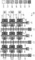
도 2의 메모리 셀(200)로서 구조체를 각각 갖는 복수 개의 메모리 셀이 논리 장치에서 메모리 셀의 어레이로서 배치된다. 메모리 셀 어레이는 비트 라인 및 워드 라인으로 체계화된다. 비트 라인 접점(247)은 메모리 셀 어레이의 비트 라인에 연결되고 게이트 접점(241)은 메모리 셀 어레이의 워드 라인에 연결된다. 도 3은 도 2의 메모리 셀을 이용하는 메모리 셀 어레이의 일부의 레이아웃 다이어그램이다. 도 3의 메모리 셀(200)을 가로지르는 단면도 A-A'는 도 2의 단면도에 대응한다.A plurality of memory cells, each having a structure as the
레이아웃 다이어그램은 그 구성을 구별짓도록 상이한 경계와 음영을 갖도록 도시된 형태를 포함한다. 형태들이 레이아웃에서 서로 오버랩할 때에, 위에 놓이고 아래에 놓이는 경계 및 음영은 오버랩의 순서를 가리키는 일 없이 도시되어 있다. 단면도는 다양한 특징부들의 수직 위치 결정을 확인하도록 사용될 수 있다. 몇몇 형태는 가변적인 기능성을 갖는 상이한 특징부에 사용된다. 예컨대, 접점을 지시하는 형태는 메모리 셀의 상이한 부분들과 접촉하고 메모리 셀 어레이의 상이한 부분들을 연결시키도록 여러 특징부에 사용될 수 있다. 형태의 범례가 제공된다. 음영(301)은 비아에 대응한다. 음영(305)은 제1 금속층(M1)에 대응하고, 음영(313)은 제2 금속층(M2)으로 대응한다. 비아(301)는 통상적으로 제1 금속층(M1)과 제2 금속층(M2) 등의 금속층들 사이에 사용된다. 음영(303)은 폴리실리콘 게이트 스택 또는 고유전율 금속 게이트 스택일 수 있는 게이트 구조에 대응한다. 음영(307)은 RRAM 구조체의 상부 전극에 대응한다. 음영(309)은 메모리 셀의 상이한 부분들과 접촉하고 메모리 셀 메모리의 상이한 부분들에 선택적으로 연결하도록 사용된다. 음영(311)은 메모리 셀에서 트랜지스터의 액티브 영역을 획정한다.Layout diagrams include shapes that are shown to have different boundaries and shading to distinguish their configuration. When the shapes overlap each other in the layout, the overlapped and underlying borders and shading are shown without indicating the order of overlaps. The cross-sectional view can be used to confirm the vertical positioning of various features. Some forms are used for different features with varying functionality. For example, the shape indicating the contact may be used for various features to contact different parts of the memory cell and to connect different parts of the memory cell array. A legend of the form is provided. The
도 3의 메모리 셀 어레이(300)의 부분은 3×3 매트릭스로 배치되는 9개의 메모리 셀(200)을 포함한다. 각 메모리 셀(200)은 트랜지스터(201)와 RRAM(203)을 포함한다. 행의 메모리 셀(200)은 게이트 구조체(303)의 일단부에서 공통의 워드 라인 픽업(317)과 게이트 구조(303)를 공유한다. 행의 메모리 셀(200)은 또한 상부 전극(307)의 일단부에서 상부 전극 픽업(315)과 RRAM 구조체의 상부 전극(307)을 공유한다. 열의 메모리 셀(200)은 제2 금속층(313)에서 비트 라인(319)을 공유한다. 메모리 셀 어레이(300)는 4개의 상이한 타입의 지점에서 접점(309)을 포함한다. 각 메모리 셀(200)에서, 접점(309)은 바닥 전극과 트랜지스터(201)의 드레인 영역 사이에서 스트레치 접점(321)으로서 사용되지만, 스트레치 접점(321) 위의 금속층에 연결된다. 각 메모리 셀(200)에서, 접점(309)은 트랜지스터(201)의 소스 영역과 접촉하고 M1 특징부(325)와 비아(327)를 통해 M2(313) 레벨에서 비트 라인(219)에 연결하도록 사용된다.The portion of the
메모리 셀(200)의 각 행을 위해, 접점(309)이 게이트 구조체(303)를 워드 라인 픽업(317)에 연결하도록 사용되고 접점(309)이 상부 전극(307)을 상부 전극 픽업(315)에 연결하도록 사용된다.A
도 4는 다양한 실시예에서 본 개시의 양태에 따른 메모리 장치를 제조하는 방법(400)의 흐름도이다. 도 4의 방법은 상이한 트랜지스터 타입(폴리실리콘 게이트 및 고유전율의 금속 게이트 등) 및 제조 프로세스(먼저 게이트 또는 마지막에 게이트와 같이)에 적응될 수 있다. 방법(400)의 다양한 작업은 도 5a 내지 도 9a 및 도 5b 내지 도 9b의 단면도 뿐만 아니라 도 5c, 도 7c 및 도 9c의 레이아웃 다이어그램과 관련하여 논의된다. 몇몇 변형예가 도 10a 내지 도 10e 및 도 11a 내지 도 11e의 단면도와 관련하여 논의되어 있다.4 is a flow diagram of a
방법(400)의 작업(401)에서, 얕은 트렌치 절연(STI; shallow trench isolatioin) 영역이 반도체 기판에 형성된다. 기판은 반도체 기판일 수 있다. 반도체 기판은 실리콘 기판일 수 있다. 별법으로서, 기판은 게르마늄 등의 다른 원소 반도체, 실리콘 탄화물을 비롯한 화합물 반도체, 실리콘 게르마늄을 비롯한 합금 반도체, 또는 그 조합물을 포함할 수 있다. 몇몇 실시예에서, 기판은 절연체 상 반도체(SOI; semiconductor on insulator) 기판이다. 기판은 P-웰 및 n-웰과 같은 도핑 영역을 포함할 수 있다. 본 개시에서, 웨이퍼는 반도체 기판과, 반도체 기판에 그리고 그 위에 형성되며 반도체 기판에 부착되는 다양한 특징부들을 포함하는 공작물이다. 웨이퍼는 다양한 제조 스테이지에 있을 수 있고 CMOS 프로세스를 이용하여 처리된다. STI 영역은 반도체 기판의 일부를 제거하여 반도체 기판에 트렌치를 형성하고 트렌치를 유전체 물질로 충전시킴으로써 형성된다. 유전체 물질은 실리콘 산화물, 실리콘 질화물, 실리콘 산질화물, 탄소 도핑된 실리콘 산화물 또는 질화물, 또는 기타 공지된 STI 물질일 수 있다. STI 영역은 트랜지스터들의 액티브 영역들을 서로 분리하고 기판에 형성된 반도체 장치들 사이에 절연을 제공한다.In
작업(403)에서, 게이트 유전체가 STI 영역과 액티브 영역을 갖는 웨이퍼 위에 증착된다. 게이트 유전체는 실리콘 산화물, 예컨대 열적으로 성장된 실리콘 산화물, 또는 금속 산화물 등의 고유전율 유전체일 수 있다. 예시적인 고유전율 유전체는 HfO2, Ta2O5, Al2O3, TiO2, TiN, ZrO2, SnO, 또는 SnO2를 포함한다. 게이트 유전체는 원자층 증착(ALD; atomic layer deposition), 플라즈마 강화된(PE; plasma enhanced) CVD(chemcal vapor deposition), 고밀도 플라즈마(HDP; high-density plasma) CVD 등의 다양한 CVD 프로세스를 비롯한 화학적 기상 증착(CVD) 프로세스를 이용하여 증착될 수 있거나, 게이트 유전체는 예컨대 열적 산화물 프로세스를 이용하여 웨이퍼 상에서 성장될 수 있다.In
작업(405)에서, 게이트 물질은 게이트 유전체 위에 증착되거나 형성된다. 다양한 실시예에 따르면, 게이트 물질은 폴리실리콘이다. 폴리실리콘은 게이트 스택을 형성하도록 게이트 유전체 물질 위에 증착된다. 작업(407)에서, 게이트 유전체와 게이트 물질은 트랜지스터 게이트와 바닥 전극으로 패터닝된다. 트랜지스터 게이트와 바닥 전극의 패터닝은 트랜지스터 게이트와 바닥 전극을 모두 갖는 하나의 포토마스크를 이용하여 수행된다. 따라서, 이 작업에서는, 논리회로 제조 프로세스에 비해 추가의 포토마스크가 사용되지 않는다. 트랜지스터 게이트와 바닥 전극의 패터닝은 웨이퍼 상에 포토레지스트를 증착하고, 포토마스크를 통해 포토레지스트의 일부를 광 복사선에 노출하며, 포토레지스트를 현상하여 일부를 제거하는 것을 포함한다. 이어서, 포토레지스트의 나머지 부분은 게이트 물질과 게이트 유전체의 원치않는 부분이 제거되는 곳에서 에칭을 패터닝하기 위한 에칭 마스크로서 작용한다.At
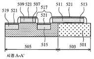
도 5a, 도 5b 및 도 5c는 단면도 예시된 부분적으로 제조된 메모리 셀과 작업(401 내지 407) 후에 오버레이 다이어그램을 도시한다. 도 5a는 도 5c의 절단선 A-A'에 따른 단면이다. 도 5b는 도 5c의 절단선 B-B'에 대응하는 단면이다. 도 5a는 STI 영역(503)과 액티브 영역(505)을 갖는 기판(501)을 도시한다. 트랜지스터 게이트는 작업(403, 405)에서 증착되는 게이트 유전체(507)와 게이트 물질(509)을 각각 포함한다. STI 영역(503) 위에 적어도 부분적으로 있고 게이트 유전체(513) 위에 전체적으로 있는 바닥 전극(511)이 트랜지스터 게이트로부터 드레인 영역(515)을 가로질러 배치된다. 드레인 영역(515)은 트랜지스터 게이트와 바닥 전극(511) 둘레의 스페이서(517)에 대해 정렬된다. 소스 영역(519)이 유사하게 정렬될 수 있다. 몇몇 실시예에서, LDD 영역(도시 생략)이 게이트 스페이서(517) 아래에 적어도 부분적으로 형성될 수 있다. 살리사이드 영역(521)은 도 5a에서 바닥 전극(511), 트랜지스터 게이트(521), 드레인 영역(515), 및 소스 영역(519) 위에 도시되어 있다.Figures 5A, 5B, and 5C illustrate overlay diagrams after partially fabricated memory cells and
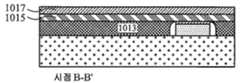
도 5b의 단면 B-B'에서, STI 부분(501)만을 갖는 기판(501)이 바닥 전극(511) 아래에 도시되어 있다. 게이트 전극(513)은 바닥 전극(511)과 기판(501) 사이에 배치된다. 스페이서(517)는 도 5a 및 도 5b에 도시된 바와 같이 바닥 전극(511)의 측면을 둘러싼다.5B, a
도 5c는 메모리 셀 어레이, 예컨대 도 3의 메모리 셀 어레이의 부분(523)의 오버레이 다이어그램이다. 도 5c는 도 5a 및 도 5b의 단면도에 대응하는 절단선 A-A' 및 B-B'를 도시하고 있다. 이들 동일한 절단선은 다양한 제조 스테이지에서 메모리 셀을 보여주도록 다음의 단면도에 사용된다.5C is an overlay diagram of a memory cell array, e.g.,
다시 도 4를 참조하면, 작업(409)에서, 트랜지스터 게이트에 인접한 반도체 기판의 다양한 영역들이 다양한 주입 영역을 형성하도록 주입된다. 다양한 주입 영역은 소스 영역 및 드레인 영역을 포함하고, 또한 저 도핑 드레인(LDD; lightly-doped drain) 등의 저 도핑 영역과 고 도핑 영역을 포함할 수 있다. 다양한 주입 영역이 트랜지스터 게이트 및 이 트랜지스터 게이트 둘레의 스페이서에 대해 정렬될 수 있다. 몇몇 실시예에서, LDD 영역이 트랜지스터 게이트 둘레에서 주입되어 트랜지스터 게이트에 정렬된다. 이어서, 트랜지스터 게이트 둘레에 스페이서가 증착된다. 추가의 주입이 스페이서와 정렬하는 소스 영역 및 드레인 영역을 형성한다. 다양한 크기의 주입 영역을 형성하도록 하나 이상의 스페이서가 사용될 수 있다. 다양한 주입 에너지 및 도판트 투여량에 의해, 고 도핑 또는 저 도핑을 갖는 얕은 또는 깊은 주입 영역이 형성된다. 일례에서, 매우 얕은 고 도핑 영역은 소스 영역 및 드레인 영역의 상부에서 웨이퍼 표면에 가깝게 형성된다. 트랜지스터 게이트 및 스페이서 등의 다양한 특징부를 이용하여 주입을 정렬시킴으로써, 작업(409)에서 포토마스크가 사용되지 않는다.Referring again to FIG. 4, at
선택적인 작업(411)에서, 살리사이드가 적어도 소스 영역과 드레인 영역 상에 형성된다. 살리사이드는 금속 박막을 실리콘과 반응시키고, 어닐링 및/또는 에칭 프로세스에 의해 형성되는 자기 정렬된 규화물이다. 살리사이드 프로세는 완전히 형성되고 패터닝된 반도체 장치(예컨대, 트랜지스터) 위에 얇은 천이 금속층의 증착에 의해 시작된다. 웨이퍼가 가열되어, 반도체 장치의 액티브 영역(예컨대, 소스, 드레인, 게이트)에서 천이 금속이 노출된 실리콘과 반응하게 하여 저저항 천이 금속 규화물을 형성한다. 천이 금속은 웨이퍼 상에 존재하는 이산화규소 또는 실리콘 질화물 절연체와 반응하지 않는다. 반응 후에, 임의의 잔존하는 천이 금속이 화학적 에칭에 의해 제거되어, 장치의 액티브 영역에서만 규화물 접점을 남겨둔다.In an optional operation 411, a salicide is formed at least on the source region and the drain region. Salicide is a self-aligned silicide formed by an annealing and / or etching process that reacts a metal film with silicon. The salicide process is initiated by the deposition of a thin transition metal layer on a fully formed and patterned semiconductor device (e.g., transistor). The wafer is heated to cause the transition metal to react with the exposed silicon at the active regions (e.g., source, drain, gate) of the semiconductor device to form a low resistance transition metal silicide. The transition metal does not react with the silicon dioxide or silicon nitride insulator present on the wafer. After the reaction, any remaining transition metal is removed by chemical etching, leaving silicide contacts only in the active area of the device.
선택적인 작업(413)에서, 트랜지스터 게이트의 게이트 물질이 제거되고 하나 이상의 상이한 게이트 물질로 교체된다. 선택적인 작업(413)은 "게이트 라스트(gate last)" 제조를 이용하여 형성되는 트랜지스터에 사용되고, 본 개시의 "게이트 라스트" 프로세스 양태를 도시하는 도 10a 내지 도 10e 및 도 11a 내지 도 11e와 관련하여 상세하게 논의된다. 게이트 물질이 작업(413)에서 교체되면, 살리사이드가 실리콘이 남았는 소스 영역 및 드레인 영역 상에 형성되고 트랜지스터 게이트 상에는 형성되지 않는다. 게이트 물질이 작업(413)에서 교체되지 않으면, 살리사이드는 게이트, 소스 영역 및 드레인 영역 상에 형성된다.In an
다시 도 4를 참조하면, 작업(415)에서, 제1 유전체 물질층이 증착된다. 제1 유전체 물질층은 RRAM의 저항성 물질층이다. 몇몇 실시예에서, 제1 유전체 물질층은 금속 산화물이고, 이 금속 산화물은 하프늄 산화물, 지르코늄 산화물, 알루미늄 산화물, 니켈 산화물, 탄탈 산화물, 티타늄 산화물, 및 저항성 물질층으로서 사용되는 기타 공지된 산화물일 수 있다. 금속 산화물은 아화학양론적 산소 대 금속 비율을 가질 수 있다. 증착 방법에 따라, 산소 대 금속 비율 및 기타 프로세스 조건은 특정한 저항성 물질층 특성을 달성하도록 조정될 수 있다. 예컨대, 한 조건 세트가 낮은 '형성' 전압을 초래할 수 있고 다른 조건 세트가 낮은 '읽기' 전압을 초래할 수 있다. 금속 산화물이 증착될 수 있다. 몇몇 실시예에서, 금속 산화물은 천이 금속 산화물이다. 다른 실시예에서, 저항성 물질층은 금속 산질화물이다.Referring again to FIG. 4, at
제1 유전체 물질층은 금속과 산소를 함유하는 전구체를 이용한 ALD와 같은 적절한 기술에 의해 형성될 수 있다. 다른 화학적 기상 증착(CVD) 기술이 사용될 수 있다. 다른 예에서, 제1 유전체 물질층은 금속 타겟 및 PVD 챔버에 대한 산소 및 선택적으로 질소의 가스 공급을 이용한 스퍼터링 프로세스와 같은 PVD에 의해 형성될 수 있다. 또 다른 예에서, 제1 유전체 물질층은 전자빔 증착 프로세스에 의해 형성될 수 있다. 제1 유전체 물질층은 약 20 옹스트롬 내지 약 200 옹스트롬의 두께를 가질 수 있다.The first layer of dielectric material may be formed by any suitable technique, such as ALD with a precursor containing metal and oxygen. Other chemical vapor deposition (CVD) techniques may be used. In another example, the first layer of dielectric material can be formed by PVD, such as a metal target and a sputtering process using oxygen and optionally nitrogen gas supply to the PVD chamber. In another example, the first layer of dielectric material may be formed by an electron beam deposition process. The first layer of dielectric material may have a thickness of from about 20 angstroms to about 200 angstroms.
작업(417)에서, 상부 전극이 제1 유전체 물질층 상에 증착된다. 상부 전극은 금속, 금속 질화물, 도핑된 폴리실리콘 또는 기타 적절한 전도성 물질일 수 있다. 예컨대, 상부 전극은 탄탈 질화물, 티타늄 질화물, 및 플라티늄일 수 있다. 상부 전극은 PVD, ALD를 비롯한 CVD, 또는 기타 적절한 기술에 의해 형성될 수 있고 약 100 옹스트롬 내지 약 2000 옹스트롬의 두께를 갖는다. 별법으로서, 상부 전극은 장치를 전기적 루트 형성을 위해 상호 연결 구조체의 다른 부분에 전기적으로 연결하도록 기타 적절한 전도성 물질을 포함한다.At
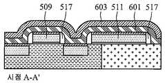
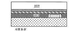
도 6a 및 도 6b는 작업(415, 417) 후에 단면도 및 오버레이 다이어그램에서 부분적으로 제조된 메모리 셀을 도시한다. 도 6a는 도 5c의 절단선 A-A'에 대응하는 단면이다. 도 6b는 도 5c의 절단선 B-B'에 대응하는 단면이다. 도 6a 및 도 6b는 트랜지스터 게이트(509)와 스페이서(517) 위에 그리고 바닥 전극(511)과 스페이서(517) 위에 정합하게 증착되는 제1 유전체 물질층(601)을 도시한다. 상부 전극 물질(603)은 또한 제1 유전체 물질층(601) 위에 정합하게 증착된다.Figures 6A and 6B illustrate memory cells partially fabricated in cross-section and overlay diagrams after task 415,417. 6A is a cross-section corresponding to the cutting line A-A 'in FIG. 5C. Fig. 6B is a cross-section corresponding to the cut line B-B 'in Fig. 5C. 6A and 6B illustrate a first layer of
다시 도 4를 참조하면, 작업(419)에서, 제1 유전체 물질층과 상부 전극 물질은 각각 RRAM 구조체 내로 패터닝된다. 패터닝은 포토레지스트가 증착되고, 포토레지스트를 노출시킴으로써 패턴이 형성되며, 포토레지스트를 현상하여 포토레지스트 패턴을 생성하는 포토리소그래피 작업을 포함한다. 이어서, 포토레지스트 패턴이 에칭 마스크로서 사용되어 RRAM 구조체의 원하는 부분을 보호한다. 이 작업에 사용되는 포토마스크는 전통적인 CMOS 제조 프로세스에서 사용되지 않는 유일한 것이다. 다른 작업에 사용되는 포토마스크는 전통적인 CMOS 제조 프로세스에서의 작업과 같이 미리 포함된다. 따라서, 본 개시의 임베디드(embedded) RRAM은 전통적인 CMOS 제조 프로세스에 비해 단 하나의 추가 포토마스크를 이용하여 그리고 RRAM 스택이 트랜지스터 위에 형성되는 다른 RRAM 제조 프로세스에 비해 적어도 2개 더 적은 포토마스크를 이용하여 제조될 수 있다. 시야 A-A'에서 도 7a에 도시된 바와 같이, 제1 유전체 물질(601)과 상부 전극 물질(603)은 액티브 영역으로부터 제거되고 바닥 전극(511)으로부터 부분적으로 제거된다. 시야 B-B'의 도 7b의 단면에서, 제1 유전체 물질(601)과 상부 전극 물질(603)은 제거되지 않는다. 도 7c에 도시된 바와 같이, 이에 따라 제1 유전체 물질(601)과 상부 전극 물질(603)의 스트립이 트랜지스터 게이트 구조체(509)에 평행한 다수의 바닥 전극을 가로질러 형성된다.Referring again to Figure 4, at
다시 도 4를 참조하면, 작업(421)에서, 층간 유전체(ILD)가 웨이퍼 위에 증착된다. 도 8a는 도 7c의 절단선 A-A'에 대응하는 단면이다. 도 8b는 도 7c의 절단선 B-B'에 대응하는 단면이다. 도 8a 및 도 8b는 트랜지스터와 RRAM 위에 ILD(801)를 도시하고 있다. ILD는 CVD 기술을 이용하여 증착된 실리콘 산화물, 실리콘 질화물, 실리콘 산질화물, 탄소 도핑된 실리콘 산화물 또는 질화물, 산소 도핑된 실리콘 탄화물일 수 있다.Referring again to FIG. 4, at
이어서, 작업(423)에서, 메모리 셀에 비트 라인 접점과 스트레치 접점이 형성된다. 작업(425)에서, 메모리 셀 어레이에 소스 라인 접점과 워드 라인 접점이 형성된다. 몇몇 실시예에서, 작업(423)과 작업(425)은 동시에 수행된다. 도 9c는 메모리 셀에서 비트 라인 접점(901)과 스트레치 접점(903) 및 메모리 셀 어레이를 위한 워드 라인 접점(905)과 소스 라인 접점(907)의 레이아웃을 도시한다. 비트 라인 접점(901)은 트랜지스터의 소스 영역(519)과 접촉한다. 스트레치 접점은 바닥 전극(511)을 드레인 영역(515)에 전기적으로 연결시킨다. 스트레치 접점은 ILD(801)에 의해 RRAM 스택으 다른 부분으로부터 분리된다. 도 9b에서, 소스 라인 접점(907)은 상부 전극(603) 위에 도시되어 있다. 도 9c의 워드 라인 접점(905)은 도 9a 및 도 9b의 어느 쪽 단면도에도 도시되어 있지 않다. 접점은 포토레지스트에 개구를 패터닝하고, ILD(801) 내로 접촉 홀을 에칭하며, 접촉 홀을 하나 이상의 접점 물질로 충전함으로써 형성된다. 몇몇 실시예에서, 하나의 포토마스크가 작업(423, 425)을 위해 사용되어 ILD(801)에서 접점(901, 903, 905, 907)을 위한 접촉 홀 모두를 형성한다.Subsequently, at
작업(423, 425) 후에, 금속층과 추가 상호 연결부가 메모리 셀 어레이 위에 형성된다. 예컨대, 유전체층(909)이 ILD(801) 및 접점(901, 905, 907) 위에 증착된다. 트렌치가 유전체층(909)에 형성되고 비트 라인(911), 소스 라인(913), 및 워드 라인(도시 생략)을 형성하도록 충전된다.After
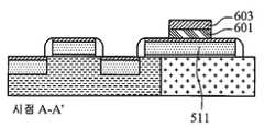
도 9c는 RRAM 메모리 셀 어레이의 일부를 도시하고 있다. 논의되는 바와 같이, 상부 전극(603)과 트랜지스터 게이트(509)는 서로 평행하다. 상부 전극(603)은 폭(W1)을 갖고, 트랜지스터 게이트(509)는 폭(W2)을 가지며, 바닥 전극(511)은 폭(W3)을 갖는다. 다양한 실시예에 따르면, 바닥 전극의 폭(W3)은 상부 전극 또는 저항성 물질층과 접촉하는 일 없이 바닥 전극(511)에 전기적으로 연결하도록 스트레치 접점(903)을 위한 충분한 공간을 갖기 위해 상부 전극의 폭(W1)보다 크다. 몇몇 실시예에서, 폭(W3)은 폭(W2)보다 적어도 50% 크고, 2배 또는 3배 클 수도 있다. 몇몇 실시예에서, 상부 전극의 폭(W1)은 트랜지스터 게이트의 폭(W2)과 대략 동일하다. 다양한 폭들은 실리콘 실제 상태의 사용을 최대화하도록 디자인 규칙을 만족시키면서 최소화된다. 따라서, 상부 전극과 저항성 물질층은 도 9a에 도시된 바와 같이 바닥 전극 상에 센터링될 수 없다. 몇몇 실시예에서, 트랜지스터로부터 상부 전극, 저항성 물질층, 및 바닥 전극의 원위 에지들이 정렬된다.9C shows a portion of an RRAM memory cell array. As discussed, the
변형예에서, 트랜지스터는 "게이트 라스트" 프로세스를 이용하여 형성된다. "게이트 라스트" 프로세스에서, 트랜지스터 제조를 위해 일시적인 폴리실리콘 게이트가 사용되고 제거된다. 이어서, 금속 게이트가 증착된다. 바닥 전극의 게이트 물질은 교체되지 않을 수 있다. 도 10a 내지 도 10e 및 도 11a 내지 도 11e는 "게이트 라스트" 프로세스를 이용하여 트랜지스터가 형성되는 메모리 셀 및 어레이의 단면을 도시하고 있다. 도 10a 내지 도 10e 및 도 11a 내지 도 11e는 도 4의 방법(400)의 다양한 작업과 관련하여 논의되지만, 도 5a 내지 도 9c에서 참조된 "게이트 퍼스트(gate first)" 프로세스와의 차이만이 상세하게 논의된다. 도 10a 내지 도 10e는 다양한 오버레이 다이어그램으로부터 시야 A-A'에 대응하는 단면도이고 도 11a 내지 도 11e는 다양한 오버레이 다이어그램으로부터 시야 B-B'에 대응하는 단면도이다.In a variant, the transistor is formed using a "gate last" process. In the " gate last "process, a temporary polysilicon gate is used and removed for transistor fabrication. A metal gate is then deposited. The gate material of the bottom electrode may not be replaced. 10A-10E and 11A-11E illustrate cross sections of memory cells and arrays in which transistors are formed using a "gate last" process. Although Figures 10a-10e and 11a-11e are discussed in connection with the various operations of the
도 10a는 작업(401, 403, 405, 407, 409, 411 및 413) 후에 시야 A-A'로부터 "게이트 라스트" 메모리 셀(1000)을 도시하고 있다. 작업은 상이한 순서로 수행될 수 있다. 몇몇 실시예에서, ILD는 게이트 물질을 교체하는 작업(413) 전에 증착된다. 도 10a에서, 게이트 물질은 트랜지스터 게이트(1001)와 바닥 전극(1003)에서 교체되었다. 소스 영역(1005)과 드레인 영역(1007)만이 살리사이드(1011, 1009)를 각각 포함한다. 게이트 물질 위의 살리사이드는 게이트 물질이 교체될 때에 제거된다. 게이트 구조체와 바닥 전극 구조체 사이에는 ILD(1013)의 평탄화 층이 배치된다. 도 11a는 도 10a에 대응하는 시야 B-B'로부터의 "게이트 라스트" 메모리 셀(1000)을 도시하고 있다. 바닥 전극(1003)은 동일 평면상의 ILD(1013)에 의해 둘러싸인다.Figure 10A shows a "gate last"
다시 도 4를 참조하면, 작업(415, 417)에서, 제1 유전체 물질층과 상부 전극층이 증착된다. 도 10b 및 도 11b는 트랜지스터 게이트, 바닥 전극, 및 ILD(1013) 위에 제1 유전체 물질층(1015)과 상부 전극층(1017)을 도시하고 있다. 도 6a 및 도 6b의 제1 유전체 물질층과 상부 전극층의 정합 형태와 달리, 여기서 이들 층은 이미 평탄화된 표면 상에 증착된다. 그 결과, 증착 프로세스 윈도우는 더 크게 되는데, 그 이유는 두께 균일도가 정합하는 특징부들의 윤곽없이 쉽게 달성되기 때문이다.Referring again to FIG. 4, in
작업(419)에서, 제1 유전체 물질층과 상부 전극층이 RRAM 구조체로 패터닝된다. 도 10c 및 도 11c는 작업(419) 후에 부분적으로 제조된 메모리 셀의 상이한 단면을 도시하고 있다. 도 10c는 트랜지스터 게이트와 바닥 전극 사이 및 제1 유전체 물질층(1015) 아래에 ILD 층(1013)의 존재를 제외하고 도 7a와 매우 유사하다. 도 11c는 도 11b과 단면도가 변하지 않는다.At
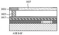
작업(421)에서, ILD(1019)는 도 10a 및 도 11d에 도시된 바와 같이, RRAM 구조체, 제1 ILD(1013), 및 트랜지스터 게이트 구조체 위에 증착된다. ILD(1019)는 제1 ILD(1013)와 동일한 물질 또는 상이한 물질일 수 있다.At
작업(423, 425)에서, ILD(1019)를 통해 트랜지스터와 RRAM 구조체에 대해 다양한 접점이 형성된다. 도 10e 및 도 11e에 도시된 바와 같이, 소스 영역(1005)에 대해 비트 라인 접점(1021)이 형성되고, 바닥 전극(1003)과 드레인 영역(1007)을 연결하도록 스트레치 접점(1023)이 형성되며, 소스 라인 접점(1025)이 상부 전극(1017)에 대해 형성된다. 추가 ILD 층(1027) 및 금속 라인(1029, 1031)이 접점 위에 제1 금속층(M1)으로서 형성된다.At
한가지 양태에서, 본 개시는 RRAM 셀에 관한 것이다. RRAM 셀은 게이트, 소스, 및 드레인 영역을 갖는 트랜지스터; 드레인 영역에 인접하고 게이트와 동일 평면 상에 있는 바닥 전극; 바닥 전극 상의 저항성 물질층; 저항성 물질층 상의 상부 전극; 및 바닥 전극을 드레인 영역에 연결하는 전도성 물질을 포함한다.In one aspect, the disclosure relates to an RRAM cell. The RRAM cell includes a transistor having a gate, a source, and a drain region; A bottom electrode adjacent to the drain region and coplanar with the gate; A layer of resistive material on the bottom electrode; An upper electrode on the resistive material layer; And a conductive material connecting the bottom electrode to the drain region.
다른 양태에서, 본 개시는 RRAM 셀 어레이에 관한 것이다. RRAM 셀 어레이는 RRAM 셀들이 다수의 워드 라인 세트로 분할되고 동일한 RRAM 셀들이 다시 다수의 비트 라인 세트로 분할되는 구조로 다수의 RRAM 셀들을 포함한다. 워드 라인 세트의 RRAM 셀들은 워드 라인 접점과 소스 라인 접점을 공유한다. 비트 라인 세트의 RRAM 셀은 비트 라인 접점을 공유한다. 메모리 셀 어레이의 각 메모리 셀은 워드 라인과 비트 라인을 이용하여 특유하게 어드레싱될 수 있다.In another aspect, the disclosure relates to an RRAM cell array. The RRAM cell array includes a plurality of RRAM cells in a structure in which RRAM cells are divided into a plurality of word line sets and the same RRAM cells are again divided into a plurality of bit line sets. The word line set of RRAM cells share a word line contact and a source line contact. The bit line set of RRAM cells share a bit line contact. Each memory cell of the memory cell array can be uniquely addressed using word lines and bit lines.
또 다른 양태에서, 본 개시는 임베디드 RRAM 셀을 구비한 논리 장치를 제조하는 방법에 관한 것이다. 방법은 반도체 기판에 얕은 트렌치 절연(STI) 영역을 형성하는 것, 게이트 유전체를 증착하는 것, 게이트 유전체 위에 게이트 물질을 증착하는 것, 게이트 유전체와 게이트 물질을 트랜지스터 게이트와 바닥 전극으로 패터닝하는 것, 트랜지스터 게이트에 인접한 반도체 기판의 영역을 주입하여 다양한 주입 영역을 형성하는 것, 제1 유전체 물질층을 증착하는 것, 제1 유전체 물질층 상에 상부 전극을 증착하는 것, 제1 유전체 물질과 상부 전극을 RRAM 구조체로 패터닝하는 것, 층간 유전체(ILD)를 증착하는 것, 및 ILD를 통해 소스 영역에 대해 비트 라인 접점을 그리고 ILD를 통해 스트레치 접점을 형성하여 바닥 전극과 드레인 영역을 연결하는 것을 포함한다. 바닥 전극의 적어도 일부가 STI 영역의 일부 위에 배치된다.In another aspect, the present disclosure relates to a method of fabricating a logic device having an embedded RRAM cell. Methods include forming a shallow trench isolation (STI) region in a semiconductor substrate, depositing a gate dielectric, depositing a gate material over the gate dielectric, patterning the gate dielectric and gate material into a transistor gate and bottom electrode, Implanting a region of the semiconductor substrate adjacent the transistor gate to form various implanted regions, depositing a first layer of dielectric material, depositing an upper electrode on the first layer of dielectric material, To the RRAM structure, depositing an interlayer dielectric (ILD), and connecting the bottom electrode and drain regions by forming a bit line contact through the ILD to the source region and a stretch contact through the ILD . At least a portion of the bottom electrode is disposed over a portion of the STI region.
전술한 내용은 여러 개의 실시예들의 특징을 개설하고 있다. 당업자라면 본 명세서에서 소개된 실시예들의 동일한 목적을 수행하고 및/또는 동일한 이점을 달성하기 위해 다른 프로세스 및 구조를 설계 또는 수정하기 위한 기초로서 본 개시를 쉽게 이용할 수 있다는 것을 알아야 한다. 당업자라면 또한 그러한 균등한 구성이 본 개시의 사상 및 범위로부터 벗어나지 않고, 본 개시의 사상 및 범위로부터 벗어남이 없이 본 명세서에 다양한 변화, 대체 및 변경이 이루어질 수 있다는 것을 알아야 한다.The foregoing has outlined features of several embodiments. It should be appreciated by those skilled in the art that the present disclosure may be readily employed as a basis for designing or modifying other processes and structures to accomplish the same objects of the embodiments disclosed herein and / or to achieve the same advantages. It should be understood by those skilled in the art that such equivalent constructions may be made without departing from the spirit and scope of this disclosure and that various changes, substitutions and alterations can be made herein without departing from the spirit and scope of the disclosure.
100: RRAM 구조체102: 기판
104: 바닥 전극106: 저항성 물질층
110: 상부 전극200: 메모리 셀
207: 게이트209: 소스 영역
211: 드레인 영역217: 채널 영역
219: 게이트 유전체100: RRAM structure 102: substrate
104: bottom electrode 106: resistive material layer
110: upper electrode 200: memory cell
207: gate 209: source region
211: drain region 217: channel region
219: gate dielectric
Claims (10)
Translated fromKorean게이트, 소스 영역, 및 드레인 영역을 갖는 트랜지스터;
상기 드레인 영역에 인접하고 상기 게이트와 동일 평면 상에 있는 바닥 전극;
상기 바닥 전극 상의 저항성 물질층;
상기 저항성 물질층 상의 상부 전극; 및
상기 바닥 전극을 상기 드레인 영역에 연결하는 전도성 물질을
포함하며,
상기 바닥 전극과 상기 게이트는 동일한 물질을 포함하고 동일한 두께를 갖는 것인, 저항성 랜덤 액세스 메모리(RRAM) 셀.A resistive random access memory (RRAM) cell,
A transistor having a gate, a source region, and a drain region;
A bottom electrode adjacent to the drain region and coplanar with the gate;
A resistive material layer on the bottom electrode;
An upper electrode on the resistive material layer; And
And a conductive material connecting the bottom electrode to the drain region
≪ / RTI &
Wherein the bottom electrode and the gate comprise the same material and have the same thickness.
반도체 기판 내에 얕은 트렌치 절연(STI; shallow trench isolation) 영역을 형성하는 단계;
게이트 유전체를 성막하는 단계;
상기 게이트 유전체 위에 게이트 물질을 성막하는 단계;
상기 게이트 유전체와 상기 게이트 물질을 트랜지스터 게이트와 바닥 전극 - 상기 바닥 전극의 적어도 일부는 상기 STI 영역의 일부 위에 배치됨 - 내로 패터닝하는 단계;
상기 트랜지스터 게이트에 인접하게 소스 영역과 드레인 영역을 형성하는 단계;
제1 유전체 물질층을 성막하는 단계;
상기 제1 유전체 물질층 상에 상부 전극 물질층을 성막하는 단계;
상기 제1 유전체 물질과 상기 상부 전극을 RRAM 구조체 내로 패터닝하는 단계;
층간 유전체(ILD; interlayer dielectric)를 성막하는 단계; 및
상기 ILD를 통해 상기 소스 영역에 대한 비트 라인 컨택을 그리고 상기 바닥 전극과 상기 드레인 영역을 연결하도록 상기 ILD를 통해 스트레치 컨택을 형성하는 단계를
포함하며,
상기 바닥 전극과 상기 트랜지스터 게이트는 동일한 물질을 포함하고 동일한 두께를 갖는, 논리 장치의 제조 방법.A method of fabricating a logic device having an embedded resistive random access memory (RRAM) cell,
Forming a shallow trench isolation (STI) region in the semiconductor substrate;
Depositing a gate dielectric;
Depositing a gate material over the gate dielectric;
Patterning the gate dielectric and the gate material into a transistor gate and bottom electrode, at least a portion of the bottom electrode being disposed over a portion of the STI region;
Forming a source region and a drain region adjacent to the transistor gate;
Depositing a first layer of dielectric material;
Depositing a top electrode material layer on the first layer of dielectric material;
Patterning the first dielectric material and the upper electrode into an RRAM structure;
Depositing an interlayer dielectric (ILD); And
Forming a bit line contact for the source region through the ILD and forming a stretch contact through the ILD to connect the bottom electrode and the drain region,
≪ / RTI &
Wherein the bottom electrode and the transistor gate comprise the same material and have the same thickness.
Applications Claiming Priority (2)
| Application Number | Priority Date | Filing Date | Title |
|---|---|---|---|
| US13/722,345 | 2012-12-20 | ||
| US13/722,345US9023699B2 (en) | 2012-12-20 | 2012-12-20 | Resistive random access memory (RRAM) structure and method of making the RRAM structure |
Publications (2)
| Publication Number | Publication Date |
|---|---|
| KR20140080401A KR20140080401A (en) | 2014-06-30 |
| KR101496006B1true KR101496006B1 (en) | 2015-02-25 |
Family
ID=50973599
Family Applications (1)
| Application Number | Title | Priority Date | Filing Date |
|---|---|---|---|
| KR20130061662AActiveKR101496006B1 (en) | 2012-12-20 | 2013-05-30 | Resistive random access memory(rram) structure and method of making the rram structure |
Country Status (3)
| Country | Link |
|---|---|
| US (3) | US9023699B2 (en) |
| KR (1) | KR101496006B1 (en) |
| TW (1) | TWI517468B (en) |
Families Citing this family (49)
| Publication number | Priority date | Publication date | Assignee | Title |
|---|---|---|---|---|
| TWI518957B (en)* | 2014-01-23 | 2016-01-21 | 林崇榮 | Resistive component of non-volatile memory and memory cell and related manufacturing method thereof |
| US10090360B2 (en) | 2015-02-13 | 2018-10-02 | Taiwan Semiconductor Manufacturing Co., Ltd. | Method of manufacturing a semiconductor structure including a plurality of trenches |
| US9525008B2 (en) | 2015-03-31 | 2016-12-20 | Taiwan Semiconductor Manufacturing Company, Ltd. | RRAM devices |
| TWI603512B (en)* | 2015-07-03 | 2017-10-21 | 力晶科技股份有限公司 | Resistive random access memory structure |
| US9685604B2 (en) | 2015-08-31 | 2017-06-20 | Taiwan Semiconductor Manufacturing Company, Ltd. | Magnetoresistive random access memory cell and fabricating the same |
| US9905751B2 (en) | 2015-10-20 | 2018-02-27 | Taiwan Semiconductor Manufacturing Company, Ltd. | Magnetic tunnel junction with reduced damage |
| US9978938B2 (en) | 2015-11-13 | 2018-05-22 | Taiwan Semiconductor Manufacturing Company, Ltd. | Resistive RAM structure and method of fabrication thereof |
| US9786674B2 (en) | 2015-11-16 | 2017-10-10 | Taiwan Semiconductor Manufacturing Company, Ltd. | Discrete storage element formation for thin-film storage device |
| US9728505B2 (en) | 2015-11-16 | 2017-08-08 | Taiwan Semiconductor Manufacturing Company, Ltd. | Methods and structrues of novel contact feature |
| US9865655B2 (en) | 2015-12-15 | 2018-01-09 | Taiwan Semiconductor Manufacturing Co., Ltd. | Memory cell structure with resistance-change material and method for forming the same |
| TWI599029B (en) | 2015-12-23 | 2017-09-11 | 華邦電子股份有限公司 | Memory devices |
| US10319675B2 (en) | 2016-01-13 | 2019-06-11 | Taiwan Semiconductor Manufacturing Company, Ltd. | Capacitor embedded with nanocrystals |
| US9685389B1 (en) | 2016-02-03 | 2017-06-20 | Taiwan Semiconductor Manufacturing Co., Ltd. | Formation of getter layer for memory device |
| JP2017174860A (en) | 2016-03-18 | 2017-09-28 | 東芝メモリ株式会社 | Semiconductor storage device and manufacturing method for the same |
| US9576653B1 (en) | 2016-05-10 | 2017-02-21 | Taiwan Semiconductor Manufacturing Co., Ltd. | Fast sense amplifier with bit-line pre-charging |
| WO2018004670A1 (en)* | 2016-07-01 | 2018-01-04 | Intel Corporation | Spatially segmented ild layer for rram-compatible ultra-scaled logic devices |
| US9792987B1 (en) | 2016-07-21 | 2017-10-17 | Taiwan Semiconductor Manufacturing Co., Ltd. | Resistive random access memory device |
| US10008253B1 (en) | 2016-08-01 | 2018-06-26 | Taiwan Semiconductor Manufacturing Co., Ltd. | Array architecture and write operations of thyristor based random access memory |
| US9660107B1 (en) | 2016-08-31 | 2017-05-23 | Taiwan Semiconductor Manufacturing Co., Ltd. | 3D cross-bar nonvolatile memory |
| US9917006B1 (en) | 2016-09-09 | 2018-03-13 | Taiwan Semiconductor Manufacturing Co., Ltd. | Method of planarizating film |
| CN107887507A (en) | 2016-09-29 | 2018-04-06 | 华邦电子股份有限公司 | Resistive random access memory, manufacturing method thereof and operating method thereof |
| WO2018063209A1 (en)* | 2016-09-29 | 2018-04-05 | Intel Corporation | Resistive random access memory cell |
| WO2018063287A1 (en)* | 2016-09-30 | 2018-04-05 | Intel Corporation | Conductive bridge resistive random access memory cell |
| US9997244B1 (en) | 2016-11-29 | 2018-06-12 | Taiwan Semiconductor Manufacturing Co., Ltd. | RRAM-based authentication circuit |
| FR3066323B1 (en)* | 2017-05-12 | 2019-11-01 | Commissariat A L'energie Atomique Et Aux Energies Alternatives | NON-VOLATILE MEMORY PROMOTING A HIGH DENSITY OF INTEGRATION |
| US10516106B2 (en)* | 2017-06-26 | 2019-12-24 | Taiwan Semiconductor Manufacturing Co., Ltd. | Electrode structure to improve RRAM performance |
| CN109671736B (en) | 2017-10-13 | 2022-09-27 | 联华电子股份有限公司 | Semiconductor structure and method of making the same |
| CN109686753B (en) | 2017-10-18 | 2022-01-11 | 联华电子股份有限公司 | Semiconductor structure and manufacturing method thereof |
| CN109698213A (en) | 2017-10-20 | 2019-04-30 | 联华电子股份有限公司 | Semiconductor structure and preparation method thereof |
| US10475725B2 (en)* | 2017-11-08 | 2019-11-12 | Texas Instruments Incorporated | Structure to enable higher current density in integrated circuit resistor |
| CN110265546B (en) | 2018-03-12 | 2022-10-14 | 联华电子股份有限公司 | Semiconductor structure and method of forming the same |
| US10880101B2 (en) | 2018-04-11 | 2020-12-29 | Taiwan Semiconductor Manufacturing Co., Ltd. | Method and circuit for de-biasing PUF bits |
| US10396126B1 (en) | 2018-07-24 | 2019-08-27 | International Business Machines Corporation | Resistive memory device with electrical gate control |
| US10727407B2 (en) | 2018-08-08 | 2020-07-28 | International Business Machines Corporation | Resistive switching memory with replacement metal electrode |
| US11088323B2 (en) | 2018-08-30 | 2021-08-10 | Taiwan Semiconductor Manufacturing Company, Ltd. | Top electrode last scheme for memory cell to prevent metal redeposit |
| US11107980B2 (en) | 2018-09-28 | 2021-08-31 | Taiwan Semiconductor Manufacturing Company, Ltd. | MRAM fabrication and device |
| KR102722905B1 (en)* | 2019-07-25 | 2024-10-30 | 삼성전자주식회사 | Semiconductor package and a method for manufacturing the same |
| US11289143B2 (en) | 2019-10-30 | 2022-03-29 | Taiwan Semiconductor Manufacturing Co., Ltd. | SOT-MRAM with shared selector |
| CN110867464B (en)* | 2019-11-21 | 2022-04-22 | 中国科学院微电子研究所 | Memristor based on 1T1R structure, preparation method thereof and integrated structure |
| WO2021206908A1 (en)* | 2020-04-07 | 2021-10-14 | Tokyo Electron Limited | In-situ encapsulation of metal-insulator-metal (mim) stacks for resistive random access memory (reram) cells |
| TWI718936B (en)* | 2020-04-17 | 2021-02-11 | 華邦電子股份有限公司 | Resistive memory device |
| TWI731688B (en)* | 2020-05-20 | 2021-06-21 | 華邦電子股份有限公司 | Three dimensional semiconductor device and methof of fabricating the same |
| TWI752642B (en)* | 2020-09-18 | 2022-01-11 | 旺宏電子股份有限公司 | Semiconductor device and method for manufacturing the same |
| US11393875B2 (en) | 2020-09-18 | 2022-07-19 | Macronix International Co., Ltd. | Semiconductor device and method for manufacturing the same |
| US11770986B2 (en) | 2021-04-22 | 2023-09-26 | International Business Machines Corporation | Etch-resistant doped scavenging carbide electrodes |
| US11917836B2 (en)* | 2021-10-28 | 2024-02-27 | United Microelectronics Corp. | Resistive random access memory structure |
| TWI797817B (en) | 2021-11-08 | 2023-04-01 | 志陽憶存股份有限公司 | Memory device and method of manufacturing the same |
| WO2024060219A1 (en)* | 2022-09-23 | 2024-03-28 | Yangtze Memory Technologies Co., Ltd. | Three-dimensional memory devices and methods for forming the same |
| TWI858692B (en)* | 2023-05-05 | 2024-10-11 | 國立勤益科技大學 | A graphene flexible memory and a method for producing the graphene flexible memory |
Citations (2)
| Publication number | Priority date | Publication date | Assignee | Title |
|---|---|---|---|---|
| KR100544085B1 (en)* | 2002-01-31 | 2006-01-23 | 샤프 가부시키가이샤 | Magnetic yoke structure of MRM device for reducing programming power consumption and method for manufacturing same |
| KR101171874B1 (en)* | 2011-02-25 | 2012-08-07 | 서울대학교산학협력단 | Non-volatile memory device and method of fabricating the same |
Family Cites Families (23)
| Publication number | Priority date | Publication date | Assignee | Title |
|---|---|---|---|---|
| US6677637B2 (en) | 1999-06-11 | 2004-01-13 | International Business Machines Corporation | Intralevel decoupling capacitor, method of manufacture and testing circuit of the same |
| TW479311B (en) | 2000-05-26 | 2002-03-11 | Ibm | Semiconductor high dielectric constant decoupling capacitor structures and process for fabrication |
| US6737728B1 (en) | 2000-10-12 | 2004-05-18 | Intel Corporation | On-chip decoupling capacitor and method of making same |
| US6919233B2 (en) | 2002-12-31 | 2005-07-19 | Texas Instruments Incorporated | MIM capacitors and methods for fabricating same |
| US6936881B2 (en) | 2003-07-25 | 2005-08-30 | Taiwan Semiconductor Manufacturing Company, Ltd. | Capacitor that includes high permittivity capacitor dielectric |
| US6940705B2 (en) | 2003-07-25 | 2005-09-06 | Taiwan Semiconductor Manufacturing Company, Ltd. | Capacitor with enhanced performance and method of manufacture |
| US6937457B2 (en) | 2003-10-27 | 2005-08-30 | Taiwan Semiconductor Manufacturing Company, Ltd. | Decoupling capacitor |
| US6849891B1 (en) | 2003-12-08 | 2005-02-01 | Sharp Laboratories Of America, Inc. | RRAM memory cell electrodes |
| US7195970B2 (en) | 2004-03-26 | 2007-03-27 | Taiwan Semiconductor Manufacturing Company, Ltd. | Metal-insulator-metal capacitors |
| US20060214213A1 (en)* | 2005-03-28 | 2006-09-28 | Fujitsu Limited | Thin-film capacitor element and semiconductor device |
| WO2007013174A1 (en)* | 2005-07-29 | 2007-02-01 | Fujitsu Limited | Resistance storage element and nonvolatile semiconductor storage device |
| KR101176543B1 (en) | 2006-03-10 | 2012-08-28 | 삼성전자주식회사 | Resistance Random Memory Device |
| US7407858B2 (en) | 2006-04-11 | 2008-08-05 | Sharp Laboratories Of America, Inc. | Resistance random access memory devices and method of fabrication |
| KR100898897B1 (en)* | 2007-02-16 | 2009-05-27 | 삼성전자주식회사 | Nonvolatile Memory Device and Formation Method |
| US7817454B2 (en)* | 2007-04-03 | 2010-10-19 | Micron Technology, Inc. | Variable resistance memory with lattice array using enclosing transistors |
| KR101418434B1 (en)* | 2008-03-13 | 2014-08-14 | 삼성전자주식회사 | Non-volatile memory device, method of fabricating the same, and processing system comprising the same |
| US7791925B2 (en) | 2008-10-31 | 2010-09-07 | Seagate Technology, Llc | Structures for resistive random access memory cells |
| US20100108980A1 (en) | 2008-11-03 | 2010-05-06 | Industrial Technology Research Institute | Resistive memory array |
| KR101526926B1 (en)* | 2008-12-30 | 2015-06-10 | 삼성전자주식회사 | Resist RAM and method of manufacturing the same |
| JP4688979B2 (en) | 2009-07-13 | 2011-05-25 | パナソニック株式会社 | Resistance change element and resistance change memory device |
| US8541819B1 (en)* | 2010-12-09 | 2013-09-24 | Monolithic 3D Inc. | Semiconductor device and structure |
| US8541765B2 (en) | 2010-05-25 | 2013-09-24 | Micron Technology, Inc. | Resistance variable memory cell structures and methods |
| DE112011102837B4 (en) | 2010-08-27 | 2021-03-11 | Semiconductor Energy Laboratory Co., Ltd. | Memory device and semiconductor device with double gate and oxide semiconductor |
- 2012
- 2012-12-20USUS13/722,345patent/US9023699B2/enactiveActive
- 2013
- 2013-05-30KRKR20130061662Apatent/KR101496006B1/enactiveActive
- 2013-12-09TWTW102145071Apatent/TWI517468B/enactive
- 2015
- 2015-04-13USUS14/684,642patent/US9356072B2/enactiveActive
- 2016
- 2016-05-27USUS15/167,905patent/US9780145B2/enactiveActive
Patent Citations (2)
| Publication number | Priority date | Publication date | Assignee | Title |
|---|---|---|---|---|
| KR100544085B1 (en)* | 2002-01-31 | 2006-01-23 | 샤프 가부시키가이샤 | Magnetic yoke structure of MRM device for reducing programming power consumption and method for manufacturing same |
| KR101171874B1 (en)* | 2011-02-25 | 2012-08-07 | 서울대학교산학협력단 | Non-volatile memory device and method of fabricating the same |
Also Published As
| Publication number | Publication date |
|---|---|
| US20140175365A1 (en) | 2014-06-26 |
| US9780145B2 (en) | 2017-10-03 |
| US20160276408A1 (en) | 2016-09-22 |
| KR20140080401A (en) | 2014-06-30 |
| US9356072B2 (en) | 2016-05-31 |
| TW201427126A (en) | 2014-07-01 |
| US9023699B2 (en) | 2015-05-05 |
| TWI517468B (en) | 2016-01-11 |
| US20150214276A1 (en) | 2015-07-30 |
Similar Documents
| Publication | Publication Date | Title |
|---|---|---|
| KR101496006B1 (en) | Resistive random access memory(rram) structure and method of making the rram structure | |
| US10038139B2 (en) | One transistor and one resistive random access memory (RRAM) structure with spacer | |
| KR100515182B1 (en) | Method of fabricating 1t1r resistive memory array | |
| US9099647B2 (en) | One transistor and one resistive (1T1R) random access memory (RAM) structure with dual spacers | |
| US9431604B2 (en) | Resistive random access memory (RRAM) and method of making | |
| KR101851101B1 (en) | A resistive random access memory (rram) with improved forming voltage characteristics and method for making | |
| TWI792079B (en) | Memory cell, menufacturing method thereof and memory device | |
| KR100675289B1 (en) | Phase change memory cell array region and manufacturing methods thereof | |
| US20210399139A1 (en) | Transistor including hydrogen diffusion barrier film and methods of forming same | |
| US11632888B2 (en) | RRAM structure with only part of variable resistive layer covering bottom electrode and method of fabricating the same | |
| US12125920B2 (en) | Dual-layer channel transistor and methods of forming same | |
| US20250194150A1 (en) | Self-aligned active regions and passivation layer and methods of making the same | |
| CN114078859A (en) | Programmable memory element | |
| KR100683852B1 (en) | Mask ROM Device of Semiconductor Device and Formation Method | |
| KR20060115703A (en) | Mask ROM Device of Semiconductor Device and Formation Method |
Legal Events
| Date | Code | Title | Description |
|---|---|---|---|
| A201 | Request for examination | ||
| PA0109 | Patent application | Patent event code:PA01091R01D Comment text:Patent Application Patent event date:20130530 | |
| PA0201 | Request for examination | ||
| E902 | Notification of reason for refusal | ||
| PE0902 | Notice of grounds for rejection | Comment text:Notification of reason for refusal Patent event date:20140415 Patent event code:PE09021S01D | |
| PG1501 | Laying open of application | ||
| E701 | Decision to grant or registration of patent right | ||
| PE0701 | Decision of registration | Patent event code:PE07011S01D Comment text:Decision to Grant Registration Patent event date:20141124 | |
| GRNT | Written decision to grant | ||
| PR0701 | Registration of establishment | Comment text:Registration of Establishment Patent event date:20150216 Patent event code:PR07011E01D | |
| PR1002 | Payment of registration fee | Payment date:20150216 End annual number:3 Start annual number:1 | |
| PG1601 | Publication of registration | ||
| FPAY | Annual fee payment | Payment date:20180206 Year of fee payment:4 | |
| PR1001 | Payment of annual fee | Payment date:20180206 Start annual number:4 End annual number:4 | |
| FPAY | Annual fee payment | Payment date:20190201 Year of fee payment:5 | |
| PR1001 | Payment of annual fee | Payment date:20190201 Start annual number:5 End annual number:5 | |
| FPAY | Annual fee payment | Payment date:20200212 Year of fee payment:6 | |
| PR1001 | Payment of annual fee | Payment date:20200212 Start annual number:6 End annual number:6 | |
| PR1001 | Payment of annual fee | Payment date:20210208 Start annual number:7 End annual number:7 | |
| PR1001 | Payment of annual fee | Payment date:20230201 Start annual number:9 End annual number:9 | |
| PR1001 | Payment of annual fee | Payment date:20240201 Start annual number:10 End annual number:10 | |
| PR1001 | Payment of annual fee | Payment date:20250204 Start annual number:11 End annual number:11 |